1
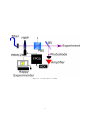
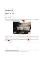
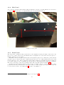
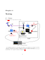
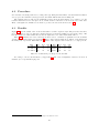
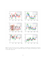
SLAP Manual Sam Bader Contents 1 Overview and Purpose 1.1 Background . . . . . . . . . . . . . . . . . . . . . . . . . . . . . . . . . . . . . . . . . . . . 1.2 Versus current configuration . . . . . . . . . . . . . . . . . . . . . . . . . . . . . . . . . . . 1.3 Overall design . . . . . . . . . . . . . . . . . . . . . . . . . . . . . . . . . . . . . . . . . . . 3 3 3 3 2 Operation 2.1 Physical setup . . . . . 2.2 Amplifier Setting . . . 2.3 Time to PID! . . . . . 2.4 What could go wrong? . . . . . . . . . . . . . . . . . . . . . . . . . . . . . . . . . . . . . . . . . . . . . . . . . . . . . . . . . . . . . . . . . . . . . . . . . . . . . . . . . . . . . . . . . . . . . . . . . . . . . . . . . . . . . . . . . . . . . . . . . . . . . . . . 5 5 6 7 8 3 Specifics of Construction 3.1 Circuitry . . . . . . . . . . . . . . 3.1.1 Schematic . . . . . . . . . . 3.1.2 Assembling the breadboard 3.2 Machining and Assembly . . . . . 3.2.1 FPGA Box . . . . . . . . . 3.2.2 Circuit . . . . . . . . . . . . 3.2.3 Back Panel . . . . . . . . . 3.2.4 Side Panel . . . . . . . . . . 3.2.5 Front Panel . . . . . . . . . . . . . . . . . . . . . . . . . . . . . . . . . . . . . . . . . . . . . . . . . . . . . . . . . . . . . . . . . . . . . . . . . . . . . . . . . . . . . . . . . . . . . . . . . . . . . . . . . . . . . . . . . . . . . . . . . . . . . . . . . . . . . . . . . . . . . . . . . . . . . . . . . . . . . . . . . . . . . . . . . . . . . . . . . . . . . . . . . . . . . . . . . . . . . . . . . . . . . . . . . . . . . . . . . . . . . . . . . . . . . . . . . . . . . . . . . . . . . . . . . . . . . . . . . . . . . . . . . . . . . . . . . . . . . . . . . . . . . . . . 10 10 10 11 13 13 14 15 17 17 4 Testing 4.1 Scheme . . . . . . . . . . . . . . . . . . . . . . . . . . . . . . . . . . . . . . . . . . . . . . 4.2 Procedure . . . . . . . . . . . . . . . . . . . . . . . . . . . . . . . . . . . . . . . . . . . . . 4.3 Results . . . . . . . . . . . . . . . . . . . . . . . . . . . . . . . . . . . . . . . . . . . . . . . 19 19 20 20 Appendices 22 A Effect on Cooling 22 . . . . . . . . . . . . B FPGALink B.1 Installation . . . . . . . . . B.2 Usage . . . . . . . . . . . . B.2.1 Converting to .xsvf: B.2.2 Starting a session . . B.2.3 Reading and Writing B.2.4 FPGA side . . . . . B.2.5 Troubleshooting . . B.2.6 General advice: . . . . . . . . . . . . . . . . . . . . . . . . . . . . . . . . . . . . . . . . . . . . . . . . . . . (from Python) . . . . . . . . . . . . . . . . . . . . . . . . . . . C USB Connector . . . . . . . . . . . . . . . . . . . . . . . . . . . . . . . . . . . . . . . . . . . . . . . . . . . . . . . . . . . . . . . . . . . . . . . . . . . . . . . . . . . . . . . . . . . . . . . . . . . . . . . . . . . . . . . . . . . . . . . . . . . . . . . . . . . . . . . . . . . . . . . . . . . . . . . . . . . . . . . . . . . . . . . . . . . . . . . . . . . . . . . . . . . . . . . . . . . . . . . . . . . . . . . . 25 25 25 25 26 26 26 26 27 28 1 D USBTMC for Tektronix Scopes D.1 Installing . . . . . . . . . . . . . . . . . . . . . . . . . . . . . . . . . . . . . . . . . . . . . D.2 Checking . . . . . . . . . . . . . . . . . . . . . . . . . . . . . . . . . . . . . . . . . . . . . D.3 Python code . . . . . . . . . . . . . . . . . . . . . . . . . . . . . . . . . . . . . . . . . . . . 2 29 29 30 30 Chapter 1 Overview and Purpose The SLAP project (Stabilizing Laser Amplitude and Polarization) will provide a polarized 422nm beam of fixed, stable intensity for the Cryoiontrap experiment. 1.1 Background The intensity of the 422nm laser at the experiment sets the saturation parameter s0 , which affects Doppler cooling through the damping parameter β as discussed in Jaroslaw’s thesis (Eq 2.57): β = −h̄k 2 4s0 (δ/Γ) 2 (1 + s0 + (2δ/Γ)2 ) From this, one could calculate directly (as shown in Appendix A) what effect a variation of 422nm intensity would have on the Doppler cooling. However, the dependence for this experiment is actually more complicated, because the controls (in the current configuration) also vary δ so as to keep the cooling steady, so this method only gives a sense of what is necessary. 1.2 Versus current configuration This project will also provide an easy computerized control for laser intensity at the experiment, as compared with the current setup. The current setup relies on a waveplate-beamsplitter combination at the output of an optical fiber to set the power level at the experiment but, as the polarization of the fiber output drifts, the intensity given by the current setup varies. Because of the way that the laser is shared among multiple experiments, adjustments before this point in the chain are outside of our control. So SLAP will PID the orientation of the waveplate to manage polarization drifts from the fiber, keeping the output at a constant value set by the experimenter. 1.3 Overall design The large-scale design of the project is shown in Figure 1.1. First, 422nm light from the fiber passes through a half-waveplate/beamsplitter combination, and the output of the PBS is further split to be (1) sent to the experiment, and (2) sampled by a Thorlabs photodiode. The photodiode signal is amplified, digitized, and forwarded to an FPGA. The FPGA adjusts the orientation of the half waveplate via a PRM1Z8 Thorlabs rotation mount in order to maintain a constant laser intensity at the experiment. The FPGA is also connected via USB to the Cryoiontrap computer, where the beautiful GUI improves experimenter morale. The various parts of this design are discussed in greater depth below. 3 Figure 1.1: Overall scheme for SLAP 4 Chapter 2 Operation 2.1 Physical setup Set up the optics as in the overall design of Figure 1.1. The FPGA, ADC, Photodiode, and Amplifier are all contained within the SLAPbox shown in Figure 2.1. Figure 2.1: SLAPbox Connect the serial cable to the motor, the USB cable to the computer, the BNC connection to the photodiode, and the power connector in the back to a wall outlet. Turn on the photodiode, and flip on the power switch in the back of the SLAPbox. Run Main.py with Python (version 3.2 or above) to launch the GUI1 . You should see something like Figure 2.2, although you’ll have to set the amplifier knobs, as in the next section, in order to have a non-clipped signal. 1 Main.py is extensively documented and there are other arguments which may be very helpful to anyone developing with this, such as for logging, verbosity, and automatic recompilation of the .xsvf. 5 Figure 2.2: Running SLAP 2.2 Amplifier Setting Figure 2.3: Apply a ninety degree rotation The signal from the photodiode should be amplified such that its range is within the range of the ADC of the SLAPbox, which accepts voltages from 0V to 3.3V. There are two controls which affect the amplification of the photodiode signal: the “course gain” on the Thorlabs PDA36A itself, and the “Amp. Gain” knob on the SLAPbox. The course setting allows you to adjust amplification by increments of 10dB from 0-70dB, and the Amp. The gain knob multiplies that result by a further gain 0-10. Using these two, you should be able to set the signal to an appropriate level as discussed below. Use the “90” button to rotate the waveplate 90◦ , which should scan the available range of the laser output power, producing a nice sinusoid as depicted in Figure 2.3. Adjust the gain knobs such that a 6 scan like this will take up a solid portion of the 0-3.3V range. In Figure 2.3, it goes from about .5V to about 2V. You want a large range for effective PIDing, but you also want to make sure you’re not clipping!2 As discussed in Section 3.1.1, you don’t need to worry about overloading the ADC in this process–it will be protected. Time-saver tip: for laser power in the tens of microwatts, it is reasonable to take the the highest or second-highest gain setting on the photodiode, and just rotate Amp. Gain until the signal looks good. 2.3 Time to PID! Figure 2.4: Use “Prep” to set for PIDing Now the SLAPbox is ready for use. First, hit the “Prep” button: this should take the waveplate on another 90◦ rotation and track the extrema, marked by red lines on the plot3 , as in Figure 2.4. Then, enter a setpoint at which to PID, and check the PID box; in Figure 2.5, we see SLAP PIDing at the setpoint 1.0. If you want to change the setpoint, hit the “%” button to send the new value to the FPGA. You should only try to PID within the safe (non-red) region, otherwise SLAP will chastize you. Congratulations, at this point you should be riding a stable signal. 2 Note that there are two possibilities for clipping. (1) The photodiode can rail if you have the course gain too high and shine a strong laser beam, in which case the sinusoid will be clipped regardless of the value of the Amp. Gain. (2) The protective diodes on the ADC can clip the signal if the total gain is too high. 3 If the lines do not appear about the extrema of the scan, then you should rerun “Prep”. 7 Figure 2.5: PIDing at 1.0 2.4 What could go wrong? First, if the signal is just awful on short timescales, you should check that the laser is locked and the set-up is curtained. If the PID is noisy or ineffective, you may consider adjusting the PID parameters, under Edit Settings, as in Figure 2.6. The parameters shown in the figure p = .3, i = .02, d = .01 were found to work well under generic conditions. Everytime SLAP starts up, it will resume with the previous PID settings. Figure 2.6: Changing PID parameters Finally, if the laser goes wild, or drops too much, it may not be possible to stay locked to a certain power level. If SLAP detects this occurence or is unable to approach the indicated value for a few seconds, you will receive an error message as in Figure 2.7. Simply follow the instructions and re-check the laser lock. 8 Figure 2.7: PID unable to lock. 9 Chapter 3 Specifics of Construction 3.1 Circuitry The circuitry component corresponds to the amplifier+ADC part of the overall scheme in Figure 1.1. 3.1.1 Schematic Figure 3.1: Overall circuitry schematic The circuit schematic is shown in Figure 3.1. The rationale for the design is discussed below: 1. Since the amplification stage is inverting, we will invert the photodiode signal from the BNC connection. So the BNC core is wired to ground and the voltage of the shell is amplified. Thus the input to the first op-amp should be a negative voltage; the course gain control on the Thorlabs PDA36A should be adjusted so this input is on the order of a couple hundred millivolts. 2. The first op-amp serves as a voltage buffer. Note: the LM6132 was used for both op-amps. 3. The second op-amp is in an inverting amplifier configuration. The input resistor is 1k, and the feedback resistor is a 10k pot, so that the gain can be finely adjusted from 0 to 10. The combination of this fine gain and the course gain on the Thorlabs PDA36A should allow SLAP to work at a wide range of powers. The 20nF capacitor in parallel with the feedback was found empirically to reduce the noise. 4. The amplified signal is then sent to a two-diode voltage clamp (Schottky diode: STMicroelectronics BAT46). I then calculated what value of resistor would be necessary to guarantee protection of the LTC2366 ADC: 10 • The ADC datasheet claims that the analog input can safely go .3V beyond its rails. That is, it can take -.3V to 3.6V. • So, if the clamp activates, the diode taking all the current must drop less than .3V in order to protect the ADC. Fortunately, the diode datasheet claims that the forward voltage drop will be less than .25V so long as the forward current is below .1mA. • Now, assume a crisis occurs at or before the amplification stage. At worst, the op-amp rails out and gives +/- 12V. So the resistor in the clamp will need to drop 12V at a current below .1mA. Thus, ideally, a 120k resistor will do. For good margin to keep the ADC away from its boundaries, I choose 200k. • It’s simple (and important) to verify empirically that the amplifier-clamp combination does not allow a voltage outside the safe range. 5. The signal is then digitized by the LTC2366 ADC. 6. An ADUM 1401 digital isolator between the ADC and the FPGA is used to separate this circuitry from from the noisy FPGA ground. 3.1.2 Assembling the breadboard Figure 3.2: PCB Layout The circuit is sodered onto a PCB using the geometry shown in Figure 3.2. Mounted components The leftmost surface-mount to DIP breakout (red) holds the two photodiodes, the middle one holds the ADC, and the upper-right one holds the digital isolator. The DIP chip at the bottom is the op-amp, and the three-pin element at the middle-right is the 3.3V regulator. The connector sockets are also soldered on. From bottom to top, the four-pin connector joins the power supply, the two-pin connector is for the pot, and the five-pin connector is to the FPGA. (The two-pin is actually a six-pin socket with two holes taped over, and the five-pin is actually a six-pin socket with one hole taped over). Connections are discussed further on. 11 Time-saving details Orientations of the chips are, in the figure shown, • The left diode must be cathode-up, and the right diode must be cathode-down. The BAT46, for whatever reason, is marked only with the number 4. The left-side of the number 4 is the cathode. • The analog side of the ADC is up. This means the text on the chip is upside-down. • The text should also be upside down on the isolator. • The text is right-side up on the op-amp. • On the particular female BNC socket used, the right pin is the core, and the left pin is the shell. Values: • The three bypass capacitors (one at the bottom right, and two on the digital isolator) are all .1uF. The remaining capacitor is the 20nF feedback. • The lower resistor is the 1k input to the amplifier, and the upper resistor is the 200k clamp resistor. The resulting layout is shown in Figure 3.3. Important note If you use a breadboard that connects some subsets of the single-pin rails of Figure 3.3 to one another, make sure to etch away those connections (scissors will do) or they will short the circuit. 12 Figure 3.3: Circuit sodered to a PCB 3.2 Machining and Assembly The SLAPbox is formed out of an LMB UNI-PAC Cabinet from Heeger1 ; holes and ports were added using the tools at the Course 8 Student Shop. 3.2.1 FPGA Box The FPGA with PMOD-serial connector is mounted in a modified version of Rich’s motor-controller box. The FPGA box has two extra holes on one side so that it can be bolted to the side of the SLAPbox, and it has an extra panel in the front to stabilize the PMOD-serial connection. Modified CorelDraw files are attached (Box.cdr and Box front.cdr). The assembled box should look like Figure 3.4. 1 Part # SS 350-9 Size H 350 W D 9 13 Figure 3.4: FPGA box 3.2.2 Circuit The circuit is just mounted to the base of the box with some 6-32 nylon stand-offs. To make each stand-off, I just Krazy-glued three nylon nuts to three nylon shafts as in Figure 3.5. Figure 3.5: Nylon stand-off Three holes were drilled into the PCB, the standoffs were screwed on, and then Krazy-glued to the base of the box, as in Figure 3.6. 14 Figure 3.6: Mounting the circuit board 3.2.3 Back Panel The back panel holds the power connector and supply. The SOLA power supply is attached to the inside of the back panel by four 4-40 screws. The power connection (92N4167 from Multicomp) is snuggled inside an acryllic holder as in Figure 3.7, and the holder2 is fastened to the outside of the case by four 1/4-20 screws. A rectangular hole in the back panel allows the power connection to be accessed from the interior. Figure 3.7: Acryllic power-connector holder Put together, the back panel can be seen in Figure 3.8. 2 The CorelDraw file for the holder is attached as PowerHolderFile.cdr. 15 Figure 3.8: Back Panel: Inside and Outside 16 3.2.4 Side Panel One of the side panels is tasked with holding the FPGA box in place, and this will have two holes in it, see Figure 3.9, matched up to a complementary pair of holes in the FPGA box. Figure 3.9: Side panel 3.2.5 Front Panel The front panel contains the 10k potentiometer for the amplifier circuitry, the BNC connection for the photodiode, a USB connection for the FPGA, and a rectangular hole so the serial connection (motor to FPGA) on Rich’s box is accessible. The BNC connection is just a female-female barrel (which requires a 1/2” drilled hole). The USB 2.0 B female connector was mounted into a square gap (produced by a .65” square punch) and a pair of 4-40 holes separated by .875”. The potentiometer just requires a single hole (dimensions given by whatever pot you use). The 1.1”x1.5” rectangular hole was produce by the (same) square punch and a bandsaw. The exact positioning of these holes is unimportant. The end result is shown in Figure 3.10. A BNC cable should run internally from the mount to the BNC connector of the circuit board. Wires should run from the potentiometer to the 2-pin connector on the circuit board. And a USB cable can be severed and sodered to the USB mount3 and run to the FPGA box. 3 To save you some time, the USB connector is mapped out in Appendix C. 17 Figure 3.10: Front Panel: Inside and Outside 18 Chapter 4 Testing 4.1 Scheme Figure 4.1 shows the setup was used for testing: Figure 4.1: Testing schematic A beamsplitter steals some of the input, from which both polarizations are measured separately (“Laser in 1” and “Laser in 2”). The feedback photodiode is also measured (“Laser Out”). The photodiodes are all connected to a Tektronix oscilliscope which provides half-second-averaged measurements to the computer as discussed in Appendix D. 19 4.2 Procedure For each run, I would (1) start the recording, then, (2) during the first minute, I would switch the shutter closed/open, after which I would (3) activate the SLAP PID if this was a PIDing run. The analysis script would use the minimum voltages from the first minute of recording to get the baseline ambient level for each photodiode, which would be subtracted out from the rest of the data. Then, each signal is normalized to its mean to produce the traces shown in Section 4.3. 4.3 Results Figure 4.2 plots the results of six one-hour runs taken over three separate days. The plots show the three photodiode traces, each one with the baseline subtracted off and normalized to the mean voltage. The left three runs were taken with PID off, and the right three were taken with SLAP PID on. Table 4.1 evaluates the noise reduction in these traces. Noisiness is quantified as the standard deviation of the signal divided by its mean 1 . We see that, without PID, the noisiness of any signal is in the many tens of percents. With PID, the noisiness of the output beam is reduced to a couple percent. Run No PID 1 No PID 2 No PID 3 In 1 23 29 15 In 2 39 51 28 Out 32 55 19 Run PID 1 PID 2 PID 3 In 1 38 29 20 In 2 72 58 44 Out 1.6 2.7 3.8 Table 4.1: Noisiness in percentage for the six runs. According to the needs mandated by Appendix A, this order-of-magnitude reduction in noise is satisfactory for experimental purposes. 1 the ambient level for each photodiode has already been subtracted off. 20 Figure 4.2: Photodiode traces of the two polarizations of the input laser beam (shown blue and green) and the output laser beam (shown red) with PID off (left) and on (right), demonstrating the reduction of noise in the output beam. 21 Appendix A Effect on Cooling The effect of the 422nm intensity on Doppler cooling is studied in the Mathematica notebook included on the next page: 22 Effect on Cooling Here we estimate how much the 422nm laser intensity can vary without significantly affecting the Doppler cooling. To get a sense of the magnitude, we use the equations for Doppler cooling of a twolevel system from Jaroslaw’ s PhD thesis. To begin, Equation (2.57) gives us the damping coefficient, Β, in terms of the saturation parameter, s0. Β@s0_D := - Ñ k2 4 s0 H∆ GL I1 + s0 + H2 ∆ GL2 M ; 2 To maximize the damping rate, we set ∆=-G/2, ∆ = - G 2; and s0=2, so that the maximum damping rate is Β@2D k2 Ñ 4 which agrees with Equation (2.58). But to see how Β varies with s0, let us normalize Β to that maximum. Β2@s0_D := Β@s0D Β@2D; Plot@Β2@s0D, 8s0, 0, 4<D 1.0 0.9 0.8 0.7 0.6 0.5 1 2 3 4 And, of course, the saturation parameter can be written in terms of the Rabi frequency, W: Printed by Wolfram Mathematica Student Edition 2 Effect_on_Cooling.nb 2 W2 s0@W_D = ; G2 Since the W is linear in the electric field, s0 is linear in intensity. So to figure out how much a percentage variation in intensity affects the damping parameter, we may simply examine the effect from that percentage variation in s0. How much can s0 vary while keeping (Β_max-Β)/Β_max < Ε ? maxs0@Ε_D := Min@Abs@2 - s0D 2 . NSolve@Β2@s0D H1 - ΕL, s0DD; In order to maintain less than 1%, 5%, and 10% variations in Β: [email protected] 0.181818 [email protected] 0.365488 [email protected] 0.480506 We must have s0 varying by less than 18%, 37%, and 48% respectively. Printed by Wolfram Mathematica Student Edition Appendix B FPGALink This project is the first in our lab to use the FPGALink library for communication between the FPGA and computer. B.1 Installation The above-linked page includes both the software (Linux, Mac, and Windows) and the User Manual. (Please read the manual.) To “install” on Linux, simply download and unpack the .tar.gz. Then add the FPGALink folder to the LD LIBRARY PATH so the shared-object files can be found. For me, this was as simple as throwing the following line into my .bashrc: export LD_LIBRARY_PATH=~/fpgalink/linux.x86_64/rel B.2 B.2.1 Usage Converting to .xsvf: When you run generate as usual, Xilinx produces a .bit file, which should be converted to a .xsvf for FPGALink. Xilinx’s Impact utility can do this in batch for you. For this purpose, I created the following batch script: setMode -bscan addDevice -p 1 -file "<PROJECT FILE>.bit" addDevice -p 2 -file "/opt/Xilinx/14.3/ISE_DS/ISE/xcf/data/xcf04s.bsd" setcable -port xsvf -file "<OUTPUT FILE>.xsvf" program -p 1 exit where PROJECT FILE is the .bit which Xilinx generates, and OUTPUT FILE is the desired .xsvf. The long file path in the middle might depend on where Xilinx is installed on your system, so check that. You can run this script with impact -batch <BATCH FILE> assuming you have the following two lines in your .bashrc export XILINX=/opt/Xilinx/14.3/ISE_DS/ISE export PATH=$XILINX/bin/lin64:$PATH Again, that first line may depend on your installation! Note: In the SLAP project, this conversion procedure can be included in the application start-up by supplying the -b switch to Main.py. 25 B.2.2 Starting a session I wrote a Python script (FPGASession.py in this project) which manages all the boilerplate of initializing an FPGALink communication with the FPGA. I imagine the script would be very useful for any other project on this platform. It returns an FPGALink handle, 1 THE_HANDLE=startSession(‘‘THE_XSVF_FILE’’) which can be used as below. The defaults of this function are configured for the Nexus2, but further arguments can be supplied for other FPGAs (see its documentation). B.2.3 Reading and Writing (from Python) Using this handle, one can write a byte to a channel like this fpgalink3.flWriteChannel(THE_HANDLE,1000,THE_CHANNEL,THE_BYTE) THE CHANNEL is the number of the channel which you would like to send your byte over (FPGALink puts 128 channels at your disposal), and 1000 is an allowed timeout. Python has a convenient function named struct.pack, which can convert numbers into lists of bytes for you. For example, to send an integer (four bytes), I might use to_bytes=[ c for c in struct.pack("!I", THE_INTEGER) ] to_bytes.reverse() for byte in to_bytes: fpgalink3.flWriteChannel(THE_HANDLE,1000,THE_CHANNEL,byte) Or one can read a channel with fpgalink3.flReadChannel(THE_HANDLE,1000,THE_CHANNEL) B.2.4 FPGA side The FPGALink User Manual discusses the FPGA end of reading and writing through the USB, which is implemented in the Communicator module of the FPGA code in the SLAP project. B.2.5 Troubleshooting Specific errors: • usb set configuration(): could not set config 1: Operation not permitted. I had to change udev permissions to connect with device. This is explained in Section 2.1 of the User Manual. • csvfPlay(): XSDRTDO failed For me, this error meant that I forgot to supply power (via the -p switch) to the Nexys2. (The Nexys2 can run on power from the USB. Note this switch should only be used with a Nexys2.) • fpgalink3.FLException: b’flLoadStandardFirmware(): Device 1443:0005 not found Unplug the FPGA. And shut it off. Take a deep breath, then try again. • usb bulk write() failed This might happen the FPGA end of the USB communication is not doing its job. Every time that I’ve run into this error, it’s because I messed with the .ucf file. Perhaps your FPGA code is not actually connected to the output pins. 2 3 1 Note: for the rest of this section, I will assume fpgalink3.py has been imported, as per the comments in this script. the constraints file in <FPGALINK FOLDER>/hdl/fx2/platforms/nexys2-500 for how this should be done. 3 Note about Xilinx: You will receive an error from the Xilinx implementation stage if you list a pin in the .ucf and don’t 2 See 26 B.2.6 General advice: • The FPGALink Users Group is very helpful. For instance, I had a bit of trouble after upgrading to Ubuntu 13.04, but resolved it and discussed it on the group. The project owner added a patch that very day. • Sections 2.3-2.7 discuss the flcli utility, which was my first go-to every time I had an issue connecting with the FPGA. Using this with the any of the supplied examples is a great way to see if the problem is with the connection/permissions/device or with your code. use it, but you might not receive any notice if you reference a pin that you didn’t actually list in the .ucf; it simply won’t be used. If your .ucf file gets dissociated from your code, Xilinx will happily optimize away all your logic and program a useless FPGA, which will fail to communicate over USB. 27 Appendix C USB Connector For reference, when sodering a USB cable to these USB mounts: 28 Appendix D USBTMC for Tektronix Scopes I used the Tektronix TDS2024C Scope we have to keep track of the photodiodes for testing. These scopes have a USB connection for this very purpose, but Tektronix software only supports Windows. Our wiki has a page linking to the USBTMC driver that one would need to do this, but I had a lot of trouble installing, so I figure it’s best to record what I needed to do. D.1 Installing 1. Follow the link, download the tar of USBTMC. 2. Extract it to some folder I’ll call USBTMC FOLDER. Note: the instructions have a typo; this command should be tar -xf usbtmc.tar 3. Install linux-source-headers: sudo apt-get install linux-headers-$(uname -r) Note that the command uname -r gets your kernel version. You’ll need it later. 4. Make sure there is a symbolic link /lib/modules/[YOUR KERNEL VERSION]/build which directs to /usr/src/[YOUR KERNEL VERSION], the latter is the folder that should have been installed in Step 3. Make sure all these KERNEL VERSIONs are the same since there may be many folders for different versions on your system. The correct one to use is whatever uname -r returns. 5. Make some updates to [USBTMC FOLDER]/usbtmc.c. This step was necessary for me because I’m running a more recent version of linux than Agilent’s USBTMC was meant for. You might be able to skip it if Step 6 “just works.” • In the includes, add on the line #include <linux/slab.h> • Change the following line .ioctl=usbtmc ioctl to .unlocked ioctl=usbtmc ioctl • In USBTMC FOLDER, run sudo make to compile • In USBTMC FOLDER, run sudo insmod ./usbtmc.ko to dynamically add the driver In USBTMC FOLDER, run sudo ./usbtmc load to create the necessary files in /dev/ 29 D.2 Checking Try asking usbtmc0 to find out whether the device is connected: cat /dev/usbtmc0 You should get something like Minor Number Manufacturer Product Serial Number 001 Tektronix, Inc. Tektronix TDS2024C C019152 indicating that it has found the device. Note that this only works on a USB 2.0 port, not a USB 3.0 port (the ones with the SS next to the trident). The device is probably connected to usbtmc1; let’s ask it to identify itself: echo *IDN?>/dev/usbtmc1 cat /dev/usbtmc1 Expect something like TEKTRONIX,TDS 2024C,C019152,CF:91.1CT FV:v24.18 When I tried this, I kept getting ”connection timed out” errors. But some mysterious combination of connecting, disconnecting, unplugging, powering back up, removing and re-adding the driver1 ,and rerunning sudo ./usbtmc load sufficed to get things working. Rerunning sudo ./usbtmc load should probably the the first shot-in-the-dark after a time-out error. If the computer is restarted, you may need to rerun sudo ./usbtmc load. Also, make sure everything is saved first, because this step has frozen my computer in the past. D.3 Python code The Python code which uses this interface to collect the data for my testing is attached in PythonForScope/. My script reads from the scope repeatedly, outputs the values to a file, and uses matplotlib to plot the data in real-time. There are three files: • USBOscilloscope.py (modified from Daq, manages the low-level GPIB) • RunIt.py (my main script) • matplotlibrc (which just ensures matplotlib gets called correctly when the script is run by the standard python interpreter). Assuming USBTMC is working, and matplotlib is installed, you can just run the script with python RunIt.py 1 To remove the driver: sudo rmmod usbtmc 30