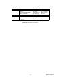
1
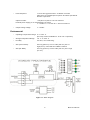
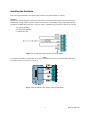
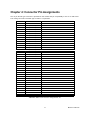
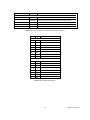
10623 Roselle Street, San Diego, CA 92121 C (858) 550-9559 C Fax (858) 550-7322
contactus@ accesio.com C www.accesio.com
MODEL LVDT-8U
EIGHT CHANNEL AC LVDT
UNIVERSAL SIGNAL CONDITIONER
USER MANUAL
MLVDT8U.B2k
Notice
The inform ation in this docum ent is provided for reference only. ACCES does not assum e any liability
arising out of the application or use of the inform ation or products described herein. This docum ent m ay
contain or reference inform ation and products protected by copyrights or patents and does not convey any
license under the patent rights of ACCES, nor the rights of others.
IBM PC, PC/XT, and PC/AT are registered tradem arks of the International Business Machines
Corporation.
Printed in USA. Copyright by ACCES I/O Products Inc, 10623 Roselle Street, San Diego, CA 92121. All
rights reserved.
WARNING!!
ALWAYS CONNECT AND DISCONNECT YOUR FIELD CABLING WITH
THE COMPUTER POWER OFF. ALWAYS TURN COMPUTER POWER
OFF BEFORE INSTALLING A CARD. CONNECTING AND
DISCONNECTING CABLES, OR INSTALLING CARDS INTO A SYSTEM
WITH THE COMPUTER OR FIELD POWER ON MAY CAUSE DAMAGE
TO THE I/O CARD AND WILL VOID ALL WARRANTIES, IMPLIED OR
EXPRESSED.
2
Manual LVDT-8U
Warranty
Prior to shipm ent, ACCES equipm ent is thoroughly inspected and tested to applicable specifications.
However, should equipm ent failure occur, ACCES assures its custom ers that prom pt service and support
will be available. All equipm ent originally m anufactured by ACCES which is found to be defective will be
repaired or replaced subject to the following considerations.
Terms and Conditions
If a unit is suspected of failure, contact ACCES' Custom er Service departm ent. Be prepared to give the
unit m odel num ber, serial num ber, and a description of the failure sym ptom (s). W e m ay suggest som e
sim ple tests to confirm the failure. W e will assign a Return Material Authorization (RMA) num ber which
m ust appear on the outer label of the return package. All units/com ponents should be properly packed for
handling and returned with freight prepaid to the ACCES designated Service Center, and will be returned
to the custom er's/user's site freight prepaid and invoiced.
Coverage
First Three Years: Returned unit/part will be repaired and/or replaced at ACCES option with no charge for
labor or parts not excluded by warranty. W arranty com m ences with equipm ent shipm ent.
Following Years: Throughout your equipm ent's lifetim e, ACCES stands ready to provide on-site or in-plant
service at reasonable rates sim ilar to those of other m anufacturers in the industry.
Equipment Not Manufactured by ACCES
Equipm ent provided but not m anufactured by ACCES is warranted and will be repaired according to the
term s and conditions of the respective equipm ent m anufacturer's warranty.
General
Under this W arranty, liability of ACCES is lim ited to replacing, repairing or issuing credit (at ACCES
discretion) for any products which are proved to be defective during the warranty period. In no case is
ACCES liable for consequential or special dam age arriving from use or m isuse of our product. The
custom er is responsible for all charges caused by m odifications or additions to ACCES equipm ent not
approved in writing by ACCES or, if in ACCES opinion the equipm ent has been subjected to abnorm al
use. "Abnorm al use" for purposes of this warranty is defined as any use to which the equipm ent is
exposed other than that use specified or intended as evidenced by purchase or sales representation.
Other than the above, no other warranty, expressed or im plied, shall apply to any and all such equipm ent
furnished or sold by ACCES.
3
Manual LVDT-8U
Table of Contents
Chapter 1: Introduction. . . . . . . . . . . . . . . . . . . . . . . . . . . . . . . . . . . . . . . . . . .
Specifications. . . . . . . . . . . . . . . . . . . . . . . . . . . . . . . . . . . . . . . . . . .
Figure 1-1: Block Diagram . . . . . . . . . . . . . . . . . . . . . . . . . . .
Installing the Hardware. . . . . . . . . . . . . . . . . . . . . . . . . . . . . . . . . . . .
Figure 1-2: Full-Bridge LVDT Sensor Term inal Schem atic. .
Figure 1-3: Half-Bridge LVDT Sensor Term inal Schem atic. .
Figure 1-4: Input Power Circuit Schem atic.. . . . . . . . . . . . . .
.
.
.
.
.
.
.
..
..
..
..
..
..
..
.
.
.
.
.
.
.
.
.
.
.
.
.
.
.
.
.
.
.
.
.
.
.
.
.
.
.
.
..
..
..
..
..
..
..
.
.
.
.
.
.
.
.
.
.
.
.
.
.
.
.
.
.
.
.
.
.
.
.
.
.
.
.
..
..
..
..
..
..
..
.
.
.
.
.
.
.
.
.
.
.
.
.
.
.
.
.
.
.
.
.
.
.
.
.
.
.
.
.
.
.
.
.
.
.
.
.
.
.
.
.
.
.
.
.
.
.
.
.
5
5
6
7
7
7
8
Chapter 2: Option Selection. . . . . .
Output Channels. . . . . . . .
Figure 2-1: Option
External Power. . . . . . . . .
.
.
.
.
.
.
.
.
.
.
.
.
.
.
.
.
.
.
.
.
.
.
.
.
.
.
.
.
.
.
.
.
.
.
.
.
.
.
.
.
.
.
.
.
.
.
.
.
.
.
.
.
.
.
.
.
.
.
.
.
.
.
.
.
.
.
.
.
.
.
.
.
.
.
.
.
9
9
9
9
........
........
Selection
........
.....
.....
Map..
.....
.
.
.
.
.
.
.
.
.
.
.
.
.
.
.
.
.
.
.
.
.
.
.
.
.
.
.
.
.
.
.
.
.
.
.
.
.
.
.
.
.
.
.
.
.
.
.
.
.
.
.
.
.
.
.
.
.
.
.
.
.
.
.
.
.
.
.
.
.
.
.
.
.
.
.
.
.
.
.
.
.
.
.
.
.
.
.
.
.
.
.
.
Chapter 3: Calibration.. . . . . . . . . . . . . . . . . . . . . . . . . . . . . . . . . . . . . . . . . . . . . . . . . . . . . . . . . . . . . . . . 10
Equipm ent Required. . . . . . . . . . . . . . . . . . . . . . . . . . . . . . . . . . . . . . . . . . . . . . . . . . . . . . . . . . . 10
Calibration Procedure. . . . . . . . . . . . . . . . . . . . . . . . . . . . . . . . . . . . . . . . . . . . . . . . . . . . . . . . . . 10
Chapter 4: Connector Pin Assignm ents. . . . . . . . . . . . . . . . . . . . . . . . . . . . . . . .
Table 4-1: DB37 Connector Pin Assignm ents, P1. . . . . . . . . . .
Table 4-2: LVDT Connections, Channel 0 through Channel 7. .
Table 4-3: Conditioned Outputs. . . . . . . . . . . . . . . . . . . . . . . . .
Table 4-4: TB9 Power Connections. . . . . . . . . . . . . . . . . . . . . .
.
.
.
.
.
.
.
.
.
.
.
.
.
.
.
.
.
.
.
.
.
.
.
.
.
.
.
.
.
.
.
.
.
.
.
.
.
.
.
.
.
.
.
.
.
.
.
.
.
.
.
.
.
.
.
.
.
.
.
.
.
.
.
.
.
.
.
.
.
.
.
.
.
.
.
.
.
.
.
.
.
.
.
.
.
.
.
.
.
.
.
.
.
.
.
11
11
12
12
13
Custom er Com m ents. . . . . . . . . . . . . . . . . . . . . . . . . . . . . . . . . . . . . . . . . . . . . . . . . . . . . . . . . . . . . . . . . 14
4
Manual LVDT-8U
Chapter 1: Introduction
This eight channel LVDT signal conditioner has been designed to be as universal as possible. By “universal”
we m ean it can provide conditioning for m any different kinds of AC LVDTs, from full-bridge to half bridge. Our
goal was to design a board that would be useful to as wide of a m arket as possible without the need to
custom ize each board for each custom er’s unique needs. Significant enhancem ents and im provem ents have
been m ade over our recent “8A” Signal Conditioner. For exam ple:
•
•
•
Addition of a 25 turn offset adjustm ent potentiom eter per channel
Synchronized excitation frequencies, Channel 0 serves as the Master while Channel’s 1
through 7 are slaves, following Channel 0's frequency.
Higher available gains for super-sensitive LVDTs and for half-bridge sensors.
At the core of the board are eight individual conditioner chips, the flexible and powerful Analog Devices
AD698.
LED Display Utility:
Six LEDs are used to display the VDC output of a Jum per Selected channel, (0 through 7). The LEDs are
labeled +10V, +5V, ZERO, -5V, and -10V. W henever the selected output voltage is within +/- 0.5 volts of
a m arked LED, that LED will be illum inated.
This utility is not intended for Calibration. It m ay be used to facilitate testing of channel(s) using on-card
resources.
Do not install m ore than one jum per at a tim e, while the card outputs are not affected, the LEDs see the
average of two channels. One jum per m ay be installed, if desired, when the card is under use.
The card has no incom ing com puter com m unications. It supplies the eight VDC outputs as described above.
If a channel is not used, no LVDT installed, that channel’s output will be near zero volts.
Specifications
The card provides power, excitation, and signal conditioning for eight independent transducers.
•
Transducers Served:
LVDT, RVDT, LVRT etc.
•
Excitation Frequency:
10 kHz.
The Frequencies m ay be specified in the range of 1Hz to 20 kHz
±10%. This is a Factory installed option which should be
specified at the tim e of purchase. Frequencies m ay be the sam e
or different for each LVDT channel.
•
Excitation Voltage:
3Vrm s.
The Voltage m ay be specified in the range of 2 to 24Vrm s.
This is a Factory installed option which should be specified at the
tim e of purchase. Voltages m ay be the sam e or different for each
LVDT channel. 40m A rm s typical per channel based on the
transducer prim ary winding im pedance.
5
Manual LVDT-8U
•
Power Required:
+9 to 36 VDC @ 700m A m ax. via DC/DC converter
Call Factory for installed power options. Should be specified at
the tim e of purchase.
Options Include:
+ 48 (36 to 75) VDC at 175 m A m axim um
External power supply (no on-board DC/DC converter)
+/- 12 VDC or +/- 15 VDC at +/- 300 m A m axim um .
•
Output Analog Voltage:
+/- 10 VDC
Environmental
•
Operating Tem perature Range: 0 EC. to 65 EC.
•
Storage Tem perature Range:
(Ext. tem p version available for -40 to +85EC operation)
-40 EC. to +100 EC.
•
Hum idity:
0 to 90%, non-condensing.
•
Size (card m odule):
8.0" long (203 m m ) X 4.74" wide (120 m m ) X 0.75"
•
Size (RT-BOX):
8.5" long (216 m m ) X 5.25" wide (133 m m ) X 2.0" high
high(19 m m ). Fits inside of RT-BOX enclosure
(51 m m ).
Figure 1-1: Block Diagram
6
Manual LVDT-8U
Installing the Hardware
The card m ay be installed in an optional steel enclosure (m odel RT-BOX or T-BOX).
Sensors:
Signals from the transducers to the card m odule are connected via rem ovable 5-pin term inal blocks
labeled TB1 through TB8. To ensure that there is m inim um susceptibility to EMI, proper EMI cabling
techniques (twisted-pair wiring and, in extrem e cases, shielded wiring) should be used on input wiring.
1-2: Prim ary W inding
3-4: Secondary W inding
5: Chassis Ground
Figure 1-2: Full-Bridge LVDT Sensor Term inal Schem atic
Note
To m inim ize possibility of extraneous noise, short term inals 3 and 4 on any unused inputs. DO NOT
ground the inputs or connect them to pin 5.
Figure 1-3: Half-Bridge LVDT Sensor Term inal Schem atic
7
Manual LVDT-8U
Pow er:
The board requires 700m A of from 9VDC to 36VDC power. Connect the +VDC lead from your power
supply to term inal block TB9 Pin 1 (labeled +15V). Connect Power Ground to TB9 Pin 2 (labeled GND.)
Under norm al circum stances, do not m ake ANY connections to TB9 Pin 3.
Figure 1-4: Input Power Circuit Schem atic
Card Pow er Options
The card requires +15 VDC and -15 VDC for internal operating power. The preferred source of this power
is from a Power Supply (DC/DC converter) installed on the card. This power supply provides a regulated
+/- 15 Volts derived from an external source within one of the two available ranges.
+12 / +24
+48
(9 to 36) VDC at 700 m A m axim um
(36 to 75) VDC at 175 m A m axim um
In addition, full +/- 10 Volt Data Outputs and a correct LED display utility which is referenced to +/- 15 Volts
will result.
An external +/- 15 Volt power supply m ay be used to power the card’s internal circuits with som e reduction
in perform ance. First, reverse voltage protective diodes are located in series with the +15 Volt and the - 15
Volt external power inputs. These diodes reduce the +/- 15 Volts to +/- 14.5 Volts approxim ately. This
Voltage reduction should not affect the +/- Data Output. However, the LED display utility will have a halfVolt error. This error m ay be corrected at the factory. If the external power supply is used to power other
external devices as well, noise generated by these devices m ay be added to the card’s DATA output.
An external +/- 12 Volt power supply is NOT recom m ended. +/- 10 Volt Data output could not be
supported, +/- 7.5 Volt Data would be the m axim um . The LED display utility would be in error up to 5 Volts,
too m uch for correction.
8
Manual LVDT-8U
Chapter 2: Option Selection
W hile no software is required to use this signal conditioner, you m ay install a software package for this
card off our m aster CD. This will install this user m anual, som e general utilities, and the card setup
program , which is intended to be used in conjunction with this m anual. All these item s will be accessible
from the start m enu (windows users).
Output Channels
All eight output channels are continuously available from output term inals labeled TB10 and TB11. These
eight channels are also available from connector P1, pins 37 through 30.
Figure 2-1: Option Selection Map
External Power
A term inal block labeled TB9, located on the corner of the board is used to connect power to the card.
W ith any on-board DC/DC converter option, only m ake connections to TB9 on the PW R term inal and
GND term inal for the return.
9
Manual LVDT-8U
Chapter 3: Calibration
Refer to the Block Diagram and Option Selection Map presented earlier in the m anual for guidance as you
perform the calibration procedure.
Equipment Required
•
•
•
A m eans of m oving the LVDT sensor in precision increm ents across the desired range of
m ovem ent (a m icrom eter jig).
An oscilloscope m ay be used to observe the prim ary and/or LVDT waveform s.
A 4 ½ digit DVM should be used for reading VDC and VAC voltages.
Calibration Procedure
Note
Reverse the connections to term inals 3 and 4 if the LVDT direction is backwards from what you desire.
1.
Read LVDT Data Sheet. Note frequency Range, Input Voltage (Excitation), and Sensitivity (m V
out per displacem ent unit). These elem ents should be com patible with the sim ilar elem ents
described below in step 2.
2.
Calibrating Channel 0: Select Display Channel 0 by placing a jum per on the Display Channel
jum per block for Channel 0. Set LVDT displacem ent to full m echanical scale or to desired
m echanical scale using the m icrom eter jig.
3.
Scaling Output: See Figure 2-1 for positions. Two 20-turn potentiom eters are used per channel to
scale the VDC output +/- 10 VDC and to adjust the offset. Adjust the LVDT to the desired positive
m echanical position, nom inally full scale. Turn the gain potentiom eter until the output reads +
10.00 volts. Adjust the LVDT to its null position. The output should be 0.0 volts, adjust the offset
potentiom eter as required. Adjust the LVDT to the desired negative position. The output should
be -10.00 volts. A slight adjustm ent of the gain and offset potentiom eters m ay be necessary to
provide the best accuracy across the full plus and m inus scale.
4.
Failure to calibrate: Not all LVDTs are alike. An LVDT m ay be m is-connected, or defective. It is
possible there is insufficient scale range for som e LVDTs. You can m ove your sensor connection
to an unused channel to confirm sensor problem s vs. board channel problem s. You are invited to
call the factory if you have a card with a problem .
5.
After com pleting the calibration of Channel 0 the rem aining seven channels m ay be installed and
calibrated using the above procedure per channel.
10
Manual LVDT-8U
Chapter 4: Connector Pin Assignments
One 37 pin D-Sub type connector is provided on the m odule with pin com patibility to one of our A/D cards.
The m ating connectors are AMP type 747304-1 or equivalent.
Pin#
1
2
3
4
5
6
7
8
9
10
11
12
13
14
15
16
17
18
19
20
21
22
23
24
25
26
27
28
29
30
31
32
33
34
35
36
37
Label
+VINEX
(UNUSED)
(UNUSED)
(UNUSED)
(UNUSED)
(UNUSED)
(UNUSED)
(UNUSED)
(UNUSED)
(UNUSED)
GROUND
(UNUSED)
(UNUSED)
(UNUSED)
(UNUSED)
(UNUSED)
(UNUSED)
GROUND
(UNUSED)
-VINEX
GROUND
GROUND
GROUND
GROUND
GROUND
GROUND
GROUND
(UNUSED)
(UNUSED)
CH 7
CH 6
CH 5
CH 4
CH 3
CH 2
CH 1
CH 0
Used for
+ 15V INPUT
GROUND
GROUND
- 15V INPUT
GROUND
GROUND
GROUND
GROUND
GROUND
GROUND
GROUND
OUTPUT
OUTPUT
OUTPUT
OUTPUT
OUTPUT
OUTPUT
OUTPUT
OUTPUT
TO
TO
TO
TO
TO
TO
TO
TO
A/D
A/D
A/D
A/D
A/D
A/D
A/D
A/D
CHANNEL
CHANNEL
CHANNEL
CHANNEL
CHANNEL
CHANNEL
CHANNEL
CHANNEL
7
6
5
4
3
2
1
0
Table 4-1: DB37 Connector Pin Assignm ents, P1
11
Manual LVDT-8U
Pin #
Label
Use
1
- Excitation
Negative, B Channel, Excitation for Channel 0 through Channel 7
2
+ Excitation
Positive, B Channel, Excitation for Channel 0 through Channel 7
3
+ Input
Positive, A Channel, Return signal from Channel 0 through Channel 7
4
- Input
Negative, A Channel, Return signal from Channel 0 through Channel 7
5
GROUND
TB1 through TB8
Table 4-2: LVDT Connections, Channel 0 through Channel 7
Pin #
Label
Use
Outputs/TB10
1
CH 0
2
GND
3
CH 1
4
GND
5
CH 2
6
GND
7
CH 3
8
GND
VDC Signal Out-0 for Channel 0
VDC Signal Out-1 for Channel 1
VDC Signal Out-2 for Channel 2
VDC Signal Out-3 for Channel 3
Outputs/TB11
1
CH 4
2
GND
3
CH 5
4
GND
5
CH 6
6
GND
7
CH 7
8
GND
VDC Signal Out-4 for Channel 4
VDC Signal Out-5 for Channel 5
VDC Signal Out-6 for Channel 6
VDC Signal Out-7 for Channel 7
Table 4-3: Conditioned Outputs
12
Manual LVDT-8U
Pin #
Label
Use
+9VDC to +36VDC, +15VDC, or
+48VDC
For ON-Card power supplies
use pin 1 and 2 only
+9VDC to +36VDC
For ON-Card
power supplies use
pin 1 and 2 only
+48VDC
For ON-Card power
supplies use pins 1
and 2 only
1
+15V
All Positive Inputs
+VDC
+48VDC
2
GND
All Ground Returns
RETURN
RETURN
3
-15V
For OFF-Card power supplies.
+/- 15V Only
No Connection
No Connection
Table 4-4: TB9 Power Connections
13
Manual LVDT-8U
Customer Comments
If you experience any problem s with this m anual or just want to give us som e feedback, please em ail us
at: manuals@ accesio.com. Please detail any errors you find and include your m ailing address so that we
can send you any m anual updates.
10623 Roselle Street, San Diego CA 92121
Tel. (858)550-9559 FAX (858)550-7322
www.accesio.com
14
Manual LVDT-8U