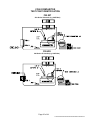
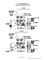
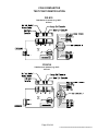
1
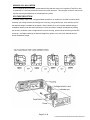
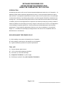
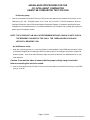
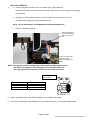
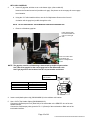
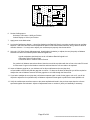
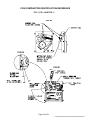
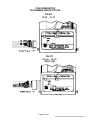
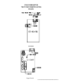
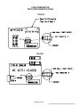
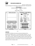
Where The Money Meets The Machine
PO Box 5128, 400 Regency Drive, Glendale Heights, IL 60139 FAX: (630) 924-7088 VOICE: (630) 924-7070
USER MANUAL
COMPARITOR TEST STATION P/N 00660009
00300009 REV. 05
2/13/2004
FRONT PANEL LAYOUT
Fig 1
OVERVIEW
The Comparitor Test Station is used to test, adjust and troubleshoot all Coin Mechanisms and other coin
validation products. The AC supply voltage is selectable, 110V, 120V, 220V, or 240VAC. The test station
has three output voltages 12VDC, 24VDC and 24VAC. Switches can be toggled to simulate a machine’s
inhibit control lines. The two counters display output signals such as the sense, credit, tilt and A, B, C
optic emulation outputs etc. A dual-color LED power indicator identifies which output voltage was
selected. The sensor coil null meter is used to check or adjust the sensor coils null and eclipse
adjustments. The “Quick connect” terminal block provides for easy hook-up for any I/O configuration.
Page 1 of 44
G:\DOC\PROCED\0030\00300009\00300009R05\00300009.DOC
Test Station Manual
CONTENTS
TOPICS
PAGE
Accessories and Display functions………………………………………………
3
JP1 Hookup Functions, Switch Functions ……………………………………...
4 & 44
Sensor Coil Null Meter and Voltage Selection …………………………………
5
CC and MC product Air Balance procedures using the Test Station…………
6–8
CC and MC product Rail and Selectivity adjustment…………………………..
8
CC and MC product Air Balance procedures using an Oscilloscope …………
9 & 10
IC product Air Balance procedures using the Test Station…………………..…
11 & 12
IC product Air Balance procedures using an Oscilloscope ………………….…
13 & 14
Defender product Air Balance procedures using the Test Station………….…
15 – 17
Defender product Air Balance procedures using an Oscilloscope ……………
18 – 20
Defender product Rail Adjustment………………………………………………..
21
PCB Test Procedures………………………………………………………………
22
Reference:
•
Coin Comparitor Identification……………………………………………….
23 & 24
•
Intelligent Comparitor Identification…………………………………………
25
•
Defender Comparitor Identification…………………………………………
26
•
Comparitor Pin Number Identification ……………………………………...
27 – 31
•
Comparitor Test Point Identification …………………………….………….
32 – 35, 40 & 41
•
IC Test Point Identification and Test Stand ……………………………….
36 – 39
•
Test Stand……………………………………………………………………..
41
•
Damper Weight Recommendations ………………………………………..
42 & 43
•
Test Station Set-up Switch configuration ………………………………….
44
Page 2 of 44
G:\DOC\PROCED\0030\00300009\00300009R05\00300009.DOC
ACCESSORIES
The following are accessories available from Coin Mechanisms Inc. or our authorized distributor for
powering your unit or assist in testing and/or adjusting a Coin Comparitor.
PART NUMBER
05000009
09280100
09280101
09280102
09280103
09300247
09300256
DESCRIPTION
Test Stand (See page 29 of 32)
I/F, “A” ASSY, 6PIN, JST, BLK/ORG/YEL,/RED/ BLU/GRY
I/F, “B” ASSY, 3 PIN JST, BLK/VIO/ORG
I/F,”C” ASSY,6PIN MOLEX/AMP GRY/RED/BLU/YEL/ORG/BLK
I/F,”D” ASSY,7PIN MOLEX/AMP,CC-62 YEL/RED/BLU /ORG/GRN/BLK
VIDEO,VHS,COMPARITOR TRAINING
VIDEO,PAL,COMPARITOR TRAINING
DISPLAY FUNCTIONS
QUICK REFERENCE TABLE
POSITIONS FOR SIGNAL SELECT SWITCHES SW9 AND SW8
SW9
SW8
DISPLAY FUNCTIONS
UP×
UP×
CREDIT and LONG TILT PULSE WIDTHS
UP×
DOWNØ
SENSE PULSE WIDTHS
DOWNØ
UP×
SINGLE CREDIT PULSE WIDTHS and EVENT also
UNWANTED TILT PULSES can be detected
DOWNØ
DOWNØ
SENSE and CREDIT EVENT
Table 1
Any output signals can be viewed individually by toggling the corresponding switches (see TABLE 1). A
dual-colored LED flashes to indicate which signal or signals are being displayed, LED red = sense or tilt,
LED green = credit. (above SW9)
The left 3-digit 7-segment display measures output signals such as the sense, credit, and tilt signals in
milliseconds.
The right 3-digit 7-segment display measures longer output signals such as the tilt signal in seconds, the
first counter overflows to the second counter and displays signals in seconds. Signals can be measured
accurately up to 15 minutes.
The right display also doubles as a coin/event counter. It can help in detecting false crediting or numerous
crediting.
Both counters utilize external reset switches (SW7, SW10) the 3-position switches can be set for manual
reset, accumulating counter or the test station’s internal auto-reset mode that occurs in approximately 2
seconds after a signal has been generated. In auto-reset mode the next new incoming signal will reset
the current signal displayed and display the new signal. Typically the manual reset (SW7) is used for coin
counting (accumulating), The millisecond counter reset switch (SW10) can typically run in the auto-reset
mode.
Page 3 of 44
G:\DOC\PROCED\0030\00300009\00300009R05\00300009.DOC
JP1-# I/O HOOKUP FUNCTIONS
For simplified choices regarding operation of the test station refer to TABLE 1 page 3.
Caution: Care must be taken to ensure that the proper voltage range is selected before connecting
the unit to be tested.
FRONT PANEL HOOK-UP: JP1-#
JP1-1 = SENSE input; sourcing signals only. (From sense output of Comparitor)
JP1-2 = OUTPUT VOLTAGE (HOT); to Comparitor, SW2 voltage select, SW3 on/off.
JP1-3 = SENSE input; open collector (O.C.) signals only. (From sense output of Comparitor)
JP1-4 = COMMON; GROUND
JP1-5 = CREDIT input; open collector signals (O.C.) only. (From credit output of Comparitor)
JP1-6 = Dual function I/O; controlled by SW4, Micro-Switch input and a +5VDC output.
• Micro-Switch input; N.O. connection only, (with internal debounce circuit) used by mechanical
Mechs. Micro-switch connection = N.O. tab to JP1-6 and switch COMM. tab to JP1-4.
• +5VDC output power supply; used for reject optics and any other 5V application.
JP1-7 = TILT input, open collector signals only. (From tilt output of Comparitor)
JP1-8 = INHIBIT control, applied by SW5 and SW6. (To inhibit pin of Comparitor interface)
SWITCH FUNCTIONS
SW1, main power switch in rear of test station.
SW7, event/sec counter reset mode.
SW2, output voltage select to Mech.
SW8 and SW9, select signal to view.
SW3, on/off power to Mech.
SW10, milli-sec. counter reset mode.
SW4, micro switch input or +5VDC output to JP1-6.
SW5, inhibit level emulation select, SW6 inhibit control emulation to Mech.
INHIBIT SWITCHES
SW5 and SW6 = INHIBIT LEVEL AND CONTROL
SW5 Configuration selects the proper inhibit level.
TOP POSITION =
3VDC or 6VDC
BOTTOM POSITION = GND.
SW6 Configuration sends the inhibit control level to JP1-8 and the Comparitor inhibit wire to disable it from
accepting coins or enable it to accept coins. Both switches can be toggled to apply the proper inhibit level
and control to the mech.
TOP POSITION =
GND or 6VDC depending on SW5 position.
MIDDLE POSITION = OFF or OPEN (Floating connection).
BOTTOM POSITION = GND. or 3VDC depending on SW5 position.
Refer to the Comparitor Specification Sheet for inhibit control and level settings.
Page 4 of 44
G:\DOC\PROCED\0030\00300009\00300009R05\00300009.DOC
SENSOR COIL NULL METER
JP2 = Comparitor Null Test Point, use banana/mini-clip lead and connect to Comparitors Test Point, refer
to schematic or Test Point identification at the end of this document. This test point is used to view the null
and the coins eclipse adjustment in microamperes dc (uADC).
VOLTAGE SELECTION
To change voltage: open cover, using small blade screwdriver or similar tool: set aside cover/fuse block
assembly: pull voltage selector card straight out of housing, using indicator pin; orient selector card so
that desired voltage is readable at the bottom; orient indicator pin to point up when desired voltage is
readable at bottom (note that when indicator pin is fixed, successive voltages are selected by rotating
the card 90° clockwise); insert voltage selector card into housing, printed side of card facing toward IEC
connector , and edge containing the desired voltage first; replace cover, and verify that indicator pin
shows the desired voltage.
Page 5 of 44
G:\DOC\PROCED\0030\00300009\00300009R05\00300009.DOC
DETAILED PROCEDURE FOR
AIR BALANCING THE SENSOR COILS
USING THE COMPARITOR TEST STATION
INTRODUCTION:
Air balancing the sensor coils is one of the most important adjustments made to the coin Comparitor. Air
balancing simply means to adjust the gap between the coils, to create an electrical field that is equal in
both coin slots. It is important to adjust both coil sensor screws on the CC product line to an equal depth
into the sensor coil body. By following this procedure, a uniform magnetic field will be maintained in the
sensing area. Coin travel and sensing metal content of coins and tokens can be made more accurately.
In addition, proper rail insert adjustment will complete the air balance procedure by providing a means to
match the resident coin to the falling coin so they “eclipse” in the sensor coils. There is no rail adjustment
on the Intelligent Comparitor product line. Another performance related adjustment is the selectivity
potentiometer. Proper selectivity adjustment will improve coin / token acceptance vs. slug rejection.
Pages 27– 31 illustrates the input/output pin assignments for the various Coin Comparitors that Coin
Mechanisms Inc. manufactures.
WHY AIR BALANCE THE SENSOR COILS ?
1) After installing a new sensor coil assembly into a Comparitor.
2) After installing a rebuilt sensor coil assembly into a Comparitor.
3) Typical maintenance procedure for optimum performance.
TOOL LIST:
1)
Various diameter, plastic tokens.
2)
1/16” hex allen head, adjusting screwdriver.
3)
Coin sticks, or coins and scotch tape.
4)
Comparitor Test Station, or power supply.
5)
Oscilloscope, optional if using the Comparitor Test Station.
Page 6 of 44
G:\DOC\PROCED\0030\00300009\00300009R05\00300009.DOC
AIR BALANCING PROCEDURES FOR
THE CC AND MICRO (MC) COMPARITOR PRODUCT
USING THE COMPARITOR TEST STATION
Preliminary setup:
NOTE: Latest version MC product have a test header, refer to pages 36 & 37 for the correct pcb that
matches your configuration.
1) Using pages 23 – 41 of this manual to determine which mechanism will be tested.
2)
Acquire schematic and/or spec sheet that corresponds with the PCB/Comparitor to be tested from Coin
Mechanisms Inc. or your local distributor.
3) Verify voltage (12VDC, 24VDC, or 24VAC) for the PCB being tested.
4) Turn voltage control knob (SW2) on test station to corresponding voltage.
Caution: Care must be taken to ensure that the proper voltage range is selected before
connecting the unit to be tested.
5) Acquire correct interface for PCB (figures 10 – 18 pages 27 - 31).
6) Connect interface wires to test station terminals in accordance with appropriate schematic/spec sheet.
7) Attach interface to PCB.
8) Toggle “Power/Tilt Reset” switch (SW3) to the ON position.
9) Verify LED on PCB lights.
10) Connect a test lead from JP2 “NULL TEST CONN” on the test station to the test point on the PCB, (see
pg. 32 – 35, 40 and 41). Illustrations show a CC-16, CC-40, CC-46 or MC equivalent, CC-62, CC-33/37,
CC-32/36 Comparitors Refer to individual Comparitor control PCB documentation (Schematic Diagram or
Comparitor specification sheet available from Coin Mechanisms Inc. or authorized distributor) for “Test
Point” location and (Voltage Spec Sheet) for power input to Comparitor models.
Air Null Balance setup:
1) Use the plastic token chip provided with Comparitor (similar in diameter) to the actual coin or token to be
used later as the sample coin and insert this chip into the sensor coils “Sample Holder”, indicated by the
label “Slide To Replace Coin”. The plastic token positions the coils in their optimum location to simulate
typical operating conditions. (see FIG. 2 page 23).
Air Null Balance adjustment :
1. Using the 1/16” allen head hex driver, back out the sensor coil screws counter-clockwise approximately ½
turn. Check the Coil Mounting Screw holding the sensor coils together for approximately 4-in. lb. of
torque. Torque this screw to 4-in. lb.
Page 7 of 44
G:\DOC\PROCED\0030\00300009\00300009R05\00300009.DOC
2. Using the 1/16” allen head hex driver, turn the Sensor Coil Adjusting Screws (see FIG. 3) page 24,
clockwise until the µA meter on the test station slightly decreases or until the screws just touch against
the center coils metal plate stop. Make sure both screws are seated with equal depth into the sensor coil
body.
3.
Start with top screw first and alternate between top and bottom screws in short 5µA intervals, with inward
(clockwise) rotation, until achieving the lowest µA reading on the µA meter.
Rail Insert adjustment setup:
1. Remove the plastic chip token from the “Sample Holder”. Insert “Coin Sticks” into the coils insuring that the
shafts of the sticks are perpendicular to the rail, using the allen screw driver turn the rail insert screw
counter-clockwise until rail insert is against the rail body, remove any slack in the assembly by applying light
pressure against the coils, towards the rail assembly (see FIG 4 & 5) page 24.
2. If “Coin Sticks” are unavailable use the coin and tape method, insert coin into the “Sample Holder“, remove
slack, apply tape to second identical coin and lower it into the other coil gap, position the taped coin in
parallel to and “eclipse” the sample coin, observe the test station µA meter for lowest reading and tape coin
in place onto the main plate.
Rail Insert adjustment:
1. The rail insert adjustment allows you to optimize the position of the resident coin to the falling coin. In order
to get the best “comparison” of coins they need to “eclipse” each other when they are in the center of the
sensor coil. The rail insert adjustment allows this exact match to occur. Performing this adjustment
optimizes against fraud coins. The adjustment also allows compensation for worn parts to bring a highly
used Comparitor back to optimum operating parameters.
2. Using the 1/16” allen hex driver, turn screw slowly clockwise (see FIG. 4 & 5) page 24, observe the µA
meter, it should lower in amplitude, keep adjusting clockwise until lowest reading can be achieved.
Remove sticks or taped coin after adjustment.
Selectivity adjustment:
1. The CC, MC and Defender products utilize a selectivity potentiometer to accommodate a wide range of coin alloys
and distributions among each alloy. The selectivity adjustment allows the user to set the Comparitor to a more
discriminative setting if a closely matching fraud is encountered or set to a more “open” setting to accept a wide
range of poorly matching coins. Turning the potentiometer clockwise on the CC and MC product sets the product
to a more discriminative setting (counterclockwise for Defender). Turning the potentiometer counterclockwise on
the CC and MC products allows the mechanism to accept a wider range of a poorly matched coin alloy (clockwise
on the Defender).
The factory potentiometer setting is typically set at a “9:00 o’clock” position (arrow pointing straight left) for most
coins. To set for the best performance/acceptance of good coins, (coins which match the sample / resident coin)
start with the pot at its most discriminative setting. Turn the pot back, counter-clockwise (clockwise for Defender)
Page 8 of 44
G:\DOC\PROCED\0030\00300009\00300009R05\00300009.DOC
in short increments, dropping coins frequently between turns, until all coins are accepted repeatedly. Fine tune as
necessary to accept all good coins or tokens and reject fraud coins.
AIR BALANCING PROCEDURES FOR
THE CC AND MICRO (MC) COMPARITOR PRODUCT
USING AN OSCILLOSCOPE
Preliminary setup:
1. Connect scope test probe to the “Mech Test Point”, (see pg. 32 – 35, 40 and 41). Illustrations show a CC16, CC-40, CC-46/MC, CC-62, CC-33/37, CC-32/36 Comparitors. Refer to individual Comparitor control
PCB documentation (Schematic Diagram or Comparitor specification sheet available from Coin
Mechanisms Inc. or authorized distributor) for “Test Point” location and (Voltage Spec Sheet) for power
input to Comparitor models. Ground the scope ground connection to the ground input for common ground.
2. Set the Scope VOLT/DIV. to 500 mv. per division.
3. Set the Scope TIME/DIV. to 1 ms. per division. Depending on type of scope, some waveform
positioning may be necessary to view the whole waveform.
Air Null Balance setup :
1. Use the plastic token chip provided with Comparitor (similar in diameter) to the actual coin or token to be
used later as the sample coin and insert this chip into the sensor coils “Sample Holder”, indicated by the
label “Slide To Replace Coin”. The plastic token positions the coils in their optimum location to simulate
typical operating conditions. (see FIG. 2) page 23.
Air Null Balance adjustment :
1. Using the 1/16” allen head hex driver, back out the sensor coil screws counter-clockwise approximately ½
turn. Check the Coil Mounting Screw holding the sensor coils together for approximately 4-in. lb. of torque.
Torque this screw to 4-in. lb. if necessary then seat the allen screws as indicated in step 3. (See FIG.5)
page 24.
2. Using the 1/16” allen head hex driver, turn the Sensor Coil Adjusting Screws (see FIG. 3) page 24,
clockwise until the wave form on the oscilloscope slightly decreases or until the screws just touch against
the center coils metal plate stop. Make sure both screws are seated with equal depth into the sensor coil
body.
3. Start with top screw first and alternate between top and bottom screws in short intervals, with inward
(clockwise) rotation, until achieving the smallest amplitude of the waveform possible. Typically 80 to 200
mV is considered to be a proper null.
Page 9 of 44
G:\DOC\PROCED\0030\00300009\00300009R05\00300009.DOC
Rail Insert adjustment setup:
1. Remove the plastic chip token from the “Sample Holder”. Insert “Coin Sticks” into the coils insuring that
the shafts of the sticks are perpendicular to the rail, using the allen screw driver turn the rail insert screw
counter-clockwise until rail insert is against the rail body, remove any slack in the assembly by applying
light pressure against the coils, towards the rail assembly (see FIG 4 & 5) page 24.
2. If “Coin Sticks” are unavailable use the coin and tape method, insert a coin into the “Sample Holder“,
remove slack, apply tape to second identical coin and lower it into the other coil gap, position the taped
coin in parallel to and “eclipse” the sample coin, observe the waveform for lowest amplitude and tape coin
in place onto the mainplate.
Rail Insert adjustment:
1. The rail insert adjustment allows you to optimize the position of the resident coin to the falling coin. In
order to get the best “comparison” of coins they need to “eclipse” each other when they are in the center of
the sensor coil. The rail insert adjustment allows this exact match to occur. Performing this adjustment
optimizes against fraud coins. The adjustment also allows compensation for worn parts to bring a highly
used Comparitor back to optimum operating parameters.
2. Using the 1/16” allen hex driver, turn screw slowly clockwise (see FIG. 4 & 5) page 24, observe the
oscilloscope, it should lower in amplitude, keep adjusting clockwise until lowest amplitude reading can be
achieved. Remove sticks or taped coin after adjustment.
Selectivity adjustment:
1. The CC, MC and Defender products utilize a selectivity potentiometer to accommodate a wide range of
coin alloys and distributions among each alloy. The selectivity adjustment allows the user to set the
Comparitor to a more discriminative setting if a closely matching fraud is encountered or set to a more
“open” setting to accept a wide range of poorly matching coins. Turning the potentiometer clockwise on
the CC and MC product sets the product to a more discriminative setting (counterclockwise for Defender).
Turning the potentiometer counterclockwise on the CC and MC products allows the mechanism to accept
a wider range of a poorly matched coin alloy (clockwise on the Defender).
The factory potentiometer setting is typically set at a “9:00 o’clock” position (arrow pointing straight left) for
most coins. To set for the best performance/acceptance of good coins, (coins which match the sample /
resident coin) start with the pot at its most discriminative setting. Turn the pot back, counter-clockwise
(clockwise for Defender) in short increments, dropping coins frequently between turns, until all coins are
accepted repeatedly. Fine tune as necessary to accept all good coins or tokens and reject fraud coins.
Page 10 of 44
G:\DOC\PROCED\0030\00300009\00300009R05\00300009.DOC
AIR BALANCE PROCEDURES FOR THE
(IC) INTELLIGENT COMPARITOR
USING THE COMPARITOR TEST STATION
Preliminary setup:
1. Connect a test lead from the Null Test Conn (JP2) on the test station to the J4 Mech Test Point pin on the
PCB (see pg. 36 - 39). Illustrations show IC-16, IC-40, IC-62, IC-33/37, IC-32/36 Comparitors. Refer to
individual Comparitor control PCB documentation (Schematic Diagram or Comparitor specification sheet
available from Coin Mechanisms Inc. or authorized distributor) for J4 location and (Voltage Spec Sheet) for
power input to Comparitor models.
NOTE: THE IC PRODUCT AIR NULL IS PERFORMMED WITHOUT USING A PLASTIC CHIP IN
THE RESIDENT COIN SIDE OF THE COILS. THE TOKEN HOLDER IS IN PLACE
WITHOUT A RESIDENT COIN.
Air Null Balance setup :
1. Start with connecting power to J1 connector (Refer to individual Mech Control PCB documentation). Refer
to Schematic Diagram and Voltage Spec Sheet for power input for the Intelligent Comparitor models and
switch on power. If the led on the PCB doesn’t light, turn power off and call Coin Mechanisms Inc or your
local distributor.
Caution: Care must be taken to ensure that the proper voltage range is selected
before connecting the unit to be tested.
2. Connect a test lead from the JP2 Null Test Conn on the test station to the Mech Test Point pin on the PCB.
(see pg. 36 to 39)
Page 11 of 44
G:\DOC\PROCED\0030\00300009\00300009R05\00300009.DOC
Air Null Balance adjustment :
1. Using the 1/16” allen head hex driver, back out the Coil Adjustment Screws (see FIG. 6 & FIG. 7) page 25,
counter- clockwise approximately ½ turn. Check the Coil Mounting Screws (see FIG. 6 page 25) holding
the sensor coils together at approximately 3-1/2 in. lbs. of torque. Verify the torque on the two screws that
hold the sensing coil stack together.
2.
Using the 1/16” allen head hex driver, turn the Coil Adjustment Screws on the front coil clockwise until the
needle on the µA meter just starts to move or until the screw just touchs against the center coil metal pin
stop.
3.
Install token holder (without sample token) in resident side of coils. Using token holder web as a
thickness gauge, slide holder in and out of coil. If token holder binds in coil, adjust screw clockwise just
until token holder clearance.
NOTE: DO NOT OVER ADJUST THIS SCREW AND CREATE AN EXCESSIVE GAP.
4. Insert the 1/16” allen wrench through the clearance hole in the spring retainer assy (see FIG. 7 page 25)
and into the allen screw location on the number 3 (back) coil assembly. Turn the screw with the allen
wrench clockwise until you get the lowest reading on the µA meter of the Comparitor Test Station (no
greater than 7 microamperes).
NOTE: Once the allen screw on the back coil bottoms (the waveform begins to get smaller),
it should not take more than a quarter turn before the lowest µA reading has been
reached. If more than a quarter turn is required to balance, contact Coin Mechanism
Inc or your local distributor.
5.
Adjust the Spring Retainer Adjustment Screw clockwise until the screw just touches the main plate. This is
to relieve strain on the #3 coil (see FIG. 7) page 25.
6. Verify the µA meter reading returns to the settings achieved in the previous steps when the coils are
squeezed together and released. Adjust coil adjustment screw on number 3 (back) coil assembly if
necessary.
Page 12 of 44
G:\DOC\PROCED\0030\00300009\00300009R05\00300009.DOC
AIR BALANCE PROCEDURES FOR THE
(IC) INTELLIGENT COMPARITOR and PRODUCT LINE
USING AN OSCILLOSCOPE
Preliminary setup:
1. Connect scope test probe to J4 “Mech Test Point” pin on the PCB (see pg. 36 to 39). Illustrations show
IC-16, IC-40, IC-62, IC-33/37, IC-32/36 Comparitors. Refer to individual Comparitor control PCB
documentation (Schematic Diagram or Comparitor specification sheet available from Coin Mechanisms
Inc. or authorized distributor) for J4 location and (Voltage Spec Sheet) for power input to Comparitor
models. Ground the scope ground connection to J4 PIN 6.
2. Set the Scope VOLT/DIV. to 500 mv. per division.
Set the Scope TIME/DIV
to
1 ms. per division. Depending on type of scope, some waveform
positioning may be necessary to view the whole waveform.
Air Null Balance setup :
1. Start with connecting power to J1 connector (Refer to individual Mech Control PCB documentation.
(Schematic Diagram) location and (Voltage Spec Sheet) for power input for the Intelligent Comparitor
models and switch on power. If the led on the PCB doesn’t light, turn power off and call Coin Mechanisms
Inc or your local distributor.
Caution: Care must be taken to ensure that the proper voltage range is selected before
connecting the unit to be tested.
2. Connect the scope probe to the Mech Test Point pin on the PCB (see pg. 36 to 39 ).
NOTE: THE IC PRODUCT AIR NULL IS PERFORMMED WITHOUT USING A PLASTIC CHIP IN
THE RESIDENT COIN SIDE OF THE COILS. THE TOKEN HOLDER IS IN PLACE
WITHOUT A RESIDENT COIN.
Page 13 of 44
G:\DOC\PROCED\0030\00300009\00300009R05\00300009.DOC
Air Null Balance adjustment :
1. Using the 1/16” allen head hex driver, back out the Coil Adjustment Screws (see FIG. 6 & FIG. 7) page 25,
counter- clockwise approximately ½ turn. Check the Coil Mounting Screws (see FIG. 6 page 25) holding
the sensor coils together at approximately 3-1/2 in. lbs. of torque. Verify the torque on the two screws that
hold the sensing coil stack together.
2. Using the 1/16” allen head hex driver, turn the Coil Adjustment Screws on the front coil clockwise until the
on the waveform just starts to move or until the screw just touchs against the center coil metal pin stop.
3. Install token holder (without sample token) in resident side of coils. Using token holder web as a
thickness gauge, slide holder in and out of coil. If token holder binds in coil, adjust screw clockwise just
until token holder clearance.
NOTE: DO NOT OVER ADJUST THIS SCREW AND CREATE AN EXCESSIVE GAP.
4. Insert the 1/16” allen wrench through the clearance hole in the spring retainer assy (see FIG. 7) page 25,
and into the allen screw location on the number 3 (back) coil assembly. Turn the screw with the allen
wrench clockwise until you get the lowest amplitude waveform on the oscilloscope (no greater than 500mV
p-p).
Note: Once the allen screw on the back coil bottoms (the waveform begins to get smaller),
it should not take more than a quarter turn before the smallest amplitude has been
reached. If more than a quarter turn is required to balance, contact Coin Mechanism
Inc or your local distributor.
5. Adjust the Spring Retainer Adjustment Screw clockwise until the screw just touches the main plate. This is
to relieve strain on the #3 coil (see FIG. 7) page 25.
6. Verify the oscilloscope waveform returns to the same amplitude achieved in the previous steps when the
coils are squeezed together and released. Adjust coil adjustment screw on number 3 (back) coil assembly
if necessary.
Page 14 of 44
G:\DOC\PROCED\0030\00300009\00300009R05\00300009.DOC
AIR BALANCE PROCEDURES FOR THE
DEFENDER COMPARITOR
USING THE COMPARITOR TEST STATION
Preliminary setup:
1. Using pages 23 – 41 of this manual determine which mechanism will be tested.
2. Acquire spec sheet that corresponds with the Comparitor to be tested from Coin Mechanisms Inc. or your
local distributor or on the web at www.coinmech.com.
Caution: Care must be taken that the correct interface is used to connect the
mechanism
to the test station.
3. Choose the correct customer interface for the test station, 0928-000113 (8 pin JST connector to flying lead) for
this test station.
4. Place the Mechanism in a test stand (CMI # 05000009).
5. Connect the interface cable to the test station and mechanism. (For connector pin outs refer to specific spec
sheets).
COIL
BALANCE
SET SCREW
SENSOR
COIL
STACK
SCREWS
There is a front (resident coin) coil balance set screw, and a back (drop slot) coil balance
set screw. Use a 1/16 Inch Allen Wrench Adjustment tool (CMI # 05090004).
6. Remove the Resident Coin, if present.
Air Null Balance adjustment :
1. Using the 1/16” allen head hex driver, back out the Coil Adjustment Screws (see FIG. 8 & 9 page 26),
counter- clockwise approximately ½ turn. Check the Coil Mounting Screws (see FIG. 9 page 26) holding
the sensor coils together at approximately 3-1/2 in. lbs. of torque. Verify the torque on the two screws that
hold the sensing coil stack together.
WITHOUT COIL GAGE BAR
2. Using the 1/16” Allen Wrench Adjustment tool, slowly tighten the front (resident coin) coil balance set screw just to
the point it bottoms out and gets a little hard to turn. Do not over tighten this setscrew. If the coils are being balanced
without using a gage bar proceed to step 9.
Page 15 of 44
G:\DOC\PROCED\0030\00300009\00300009R05\00300009.DOC
WITH COIL GAGE BAR
3.
a.
Insert coil gage bar, with the curve on the bottom right, (refer to table #2)
between the first and second coil (resident coin gap). See picture on the next page for correct gage
bar orientation.
b. Using the 1/16” allen head hex driver, turn the Coil Adjustment Screw on the front coil
clockwise until the gage bar just falls through the coils.
NOTE: DO NOT OVER ADJUST THIS SCREW AND CREATE AN EXCESSIVE GAP.
c.
Remove coil balance gage bar.
Insert gage bar with
the curve towards the
coils or on the right
side
Insert 1/16” allen head
screw driver into
Sensor coil adjustment
screw
NOTE: The gage bar used for coil balancing is determined by the #2 coil part number.
See Table #2 on page21 for the correct gage bar for the different #2 coils.
See Fig 8 page 30 for the location of the #2 coil part number and format.
Location of #2 coil
part number.
#2 Coil Part Number
925 111
925 123
925 124
Gage Bar part number
04700026
04700027
04700033
4. Insert a small plastic poker chip (CMI # 04090014) in the resident coin location.
5. Use a12-Pin Test Header Cable 0928-000151 (12 pin Molex connector to 3 wire flying lead) interface.
Page 16 of 44
G:\DOC\PROCED\0030\00300009\00300009R05\00300009.DOC
J6 10-Pin
Coil Stack Conn
Q6
Pin 1
J2 3-Pin
Rail Optic
U5
J1 8-Pin
Customer Interface
U11
U3
J7 12-Pin
Test Header
U8 TO-220
MC7805
Pin 1
Pin 1
LED
C13
18
16 14 12 10
Z8 Micro
1 2 3 4 5 6 7 8 9
C14
Y1
POT
1
Main PC Board (0927-000570)
6. Connect the 0928-000132 interface from the Mechanism test header to JP3 “MECH TEST HEADER” of the test
station.
7. Apply power to the Mechanism.
8. Monitor the µA meter on the Test Station.
9. Using the 1/16” Allen Wrench Adjustment tool, slowly tighten (clockwise), or adjust, the rear (drop slot) coil balance
setscrew to achieve the smallest possible Raw Null signal level.
A good null should achieve an air null balance of 0 to 6µA on the µA meter.
NOTE:
Once the allen screw on the back coil bottoms (the waveform begins to get smaller),
it should not take more than a quarter turn before the lowest µA meter reading
has been reached. If more than a quarter turn is required to balance, contact Coin
Mechanism Inc or your local distributor.
NOTE: On this Test Station, the Tilt display will continuously increment while balancing the coils.
If a good air coil balance cannot be achieved, then there could be a problem with the coil set or the main PC board.
In most cases if a good coil air balance cannot be achieved then the coil set needs to be replaced.
10. Insert coil balance gage bar or your thickest coin for this model between the rear (drop slot)
coil and middle coil and verify that the gage bar or coin fits. If it does not fit down the drop slot
you will be required to readjust the rear coil balance setscrew until the gage bar or coin falls
through.
11. If you had to readjust the rear (drop slot) coil balance setscrew again in order for the gage or coin to fit, you
will be required to adjust the front (resident slot) coil balance adjustment screw again to produce the lowest
possible null.
12. Verify the µA METER reading returns to the settings achieved in the previous steps when the coils are
squeezed together and released. Adjust coil adjustment screw on number 3 (back) coil assembly if
necessary.
Page 17 of 44
G:\DOC\PROCED\0030\00300009\00300009R05\00300009.DOC
AIR BALANCE PROCEDURES FOR THE
DEFENDER COMPARITOR
USING AN OSCILLOSCOPE
Preliminary setup:
Preliminary setup:
1. Using pages 23 – 41 of this manual determine which mechanism will be tested.
2. Acquire spec sheet that corresponds with the Comparitor to be tested from Coin Mechanisms Inc. or your
local distributor or on the web at www.coinmech.com.
Caution: Care must be taken that the correct interface is used to connect the
mechanism to the test station.
3. Choose the correct customer interface for the test station being used, 0928-000113 (8 pin JST connector to
flying lead) for this test station.
4. Place the Mechanism in a test stand (CMI # 05000009).
5. Connect the interface cable to the test station and mechanism. (For connector pin outs refer to specific spec
sheets).
COIL
BALANCE
SET SCREW
SENSOR
COIL
STACK
SCREWS
There is a front (resident coin) coil balance set screw, and a back (drop slot) coil balance
set screw. Use a 1/16 Inch Allen Wrench Adjustment tool (CMI # 05090004).
6. Remove the Resident Coin, if present.
Air Null Balance adjustment :
1.
Using the 1/16” allen head hex driver, back out the Coil Adjustment Screws (see FIG. 8 & 9 page 26),
counter- clockwise approximately ½ turn. Check the Coil Mounting Screws (see FIG. 9 page 26) holding
the sensor coils together at approximately 3-1/2 in. lbs. of torque. Verify the torque on the two screws that
hold the sensing coil stack together.
WITHOUT COIL GAGE BAR
2. Using the 1/16” Allen Wrench Adjustment tool, slowly tighten the front (resident coin) coil balance set screw just to
the point it bottoms out and gets a little hard to turn. Do not over tighten this setscrew. If the coils are being balanced
without using a gage bar proceed to step 9.
Page 18 of 44
G:\DOC\PROCED\0030\00300009\00300009R05\00300009.DOC
WITH COIL GAGE BAR
3.
a.
Insert coil gage bar, with the curve on the bottom right, (refer to table #2)
between the first and second coil (resident coin gap). See picture on the next page for correct gage
bar orientation.
b. Using the 1/16” allen head hex driver, turn the Coil Adjustment Screw on the front coil
clockwise until the gage bar just falls through the coils.
NOTE: DO NOT OVER ADJUST THIS SCREW AND CREATE AN EXCESSIVE GAP.
c.
Remove coil balance gage bar.
Insert gage bar with
the curve towards the
coils or on the right
side
Insert 1/16” allen head
screw driver into
Sensor coil adjustment
screw
NOTE: The gage bar used for coil balancing is determined by the #2 coil part number.
See Table #2 on page21 for the correct gage bar for the different #2 coils.
See Fig 8 page 30 for the location of the #2 coil part number and format.
Location of #2 coil
part number.
#2 Coil Part Number
925 111
925 123
925 124
Gage Bar part number
04700026
04700027
04700033
4. Insert a small plastic poker chip (CMI # 04090014) in the resident coin location.
5. Use a 12-Pin Test Header Cable (CMI #0928-000151).
Connect an Oscilloscope to Pin 6 (Raw Null) of the test header or the GRN/YEL wire of the test
header interface.
Connect the Oscilloscope probe ground to Pin 11 (Ground) of the test header or Black wire of the
test header interface.
Page 19 of 44
G:\DOC\PROCED\0030\00300009\00300009R05\00300009.DOC
J6 10-Pin
Coil Stack Conn
Q6
Pin 1
J2 3-Pin
Rail Optic
U5
U11
U3
J7 12-Pin
Test Header
U8 TO-220
MC7805
J1 8-Pin
Customer Interface
Pin 1
Pin 1
LED
C13
18
16 14 12 10
Z8 Micro
1 2 3 4 5 6 7 8 9
C14
Y1
POT
1
Main PC Board (0927-000570)
6. Set the Oscilloscope to:
Horizontal Time base to 100uS per Division.
Vertical Display to 100 mV per Division.
7. Apply power to the Mechanism.
8. Look at the Oscilloscope display. It should be displaying the Raw Null Signal, a complex waveform that can oscillate
between 7 and 9 KHz and can have an amplitude of about 9 volts Peak-to-Peak maximum, and go down to about 50
millivolts minimum. You may have to adjust your oscilloscope to properly view the waveform.
9. Using the 1/16” Allen Wrench Adjustment tool, slowly tighten (clockwise), or adjust, the rear (drop slot) coil balance
setscrew to achieve the smallest possible Raw Null signal level.
A good mechanism should achieve an air coil balance Raw Null signal level
of less than 700 mV Peak-to-Peak,
or less than 400 mV Positive Peak to Ground.
If a good air coil balance cannot be achieved, then there could be a problem with the coil set or the main PC board.
In most cases if a good coil air balance cannot be achieved then the coil set needs to be replaced.
10. Insert coil balance gage bar or your thickest coin for this model between the rear (drop slot)
coil and middle coil and verify that the gage bar or coin fits. If it does not fit down the drop slot you will be required to
readjust the rear coil balance setscrew until the gage bar or coin falls through the Sense coils.
11. If you had to readjust the rear (drop slot) coil balance setscrew again in order for the gage or coin to fit, you will be
required to adjust the front (resident slot) coil balance adjustment screw again to produce the lowest possible null.
12. Verify the oscilloscope waveform returns to the same amplitude achieved in the previous steps when the coils are
squeezed together and released. Adjust coil adjustment screw on number 3 (back) coil assembly if necessary.
Page 20 of 44
G:\DOC\PROCED\0030\00300009\00300009R05\00300009.DOC
DEFENDER RAIL ADJUSTMENT PROCEDURE
DROP SLOT DIAMETER CLEARANCE
1)
Insert proper resident coin for the model to be adjusted.
2)
Turn the side rail set screw out (Counterclockwise) one full turn.
3)
Drop a good coin into the drop slot, it should get stuck. If the coin does not get stuck, push the coil set (with the resident coin
installed) toward the rail (left) (this should force the rail insert in). Drop another good coin into the drop slot, the coin should get
stuck. If the coin still does not get stuck, contact Coin Mechanisms Inc.
NOTE: The unit may Tilt during the Drop Slot Diameter clearance adjustment procedure.
4)
Turn the side rail set screw (using a .050” hex driver or CMI P/N 05090023) in (Clockwise) until the coin falls through the
mechanism.
Drop more good coins and slightly adjust the side rail set screw until all the test coins fall freely through the mechanism.
5)
Turn the side rail set screw an additional ¼ turn in (Clockwise) for some additional diameter clearance.
CUSTOMER
INTERFACE
CONNECTOR
SIDE RAIL SET SCREW
6)
Side View of Unit
Drop good coins through the unit.
The unit should Accept 100% of the good coins.
Each coin should generate a Sense and Credit Pulse (if applicable) as the coin falls through the mechanism
The POT setting may need to be adjusted to achieve 100% acceptance if the test coins have a wide conductivity spread.
7)
Check the Diameter Optics.
Drop 0.040 Inch shaved coins through the unit under test.
The unit should Reject 100% of the shaved coins.
Page 21 of 44
G:\DOC\PROCED\0030\00300009\00300009R05\00300009.DOC
PCB TEST PROCEDURES
1. Acquire spec sheet that corresponds with the PCB to be tested.
2. Acquire spec sheet that corresponds with the Comparitor to be tested from Coin Mechanisms Inc. or your
local distributor or on the web at www.coinmech.com.
Caution: Care must be taken that the correct interface is used to connect the
mechanism to the test station.
3. Attach PCB to appropriate test chassis (Green accept coil wires for 12VDC, Gray accept coils for
24VDC/24VAC).
Note: Test chassis should be a known good chassis.
4. Attach interface to PCB.
5. Toggle “INTERFACE POWER” switch to the ON position.
6. Verify LED on PCB lights.
7. Insert small Poker chip in resident coin location of coils.
8. If the mechanisms you are testing does not have a test header; connect the 0821-009080 to the BNC
connector on the test station. Connect the 0821-009081 BNC to minigrabber clip to the 0821-009080 BNC
cable and the RED minigrabber clip to the “TEST POINT”. See pg. 32 – 41 for “Test Point” location.
a. If the mechanism you are testing has a test header, connect the correct interface (refer to spec
sheet) to the “TEST HEADER” connection on the test station. Connect the other end of the interface
to the test header on the PCB.
b. Verify DC VOLT METER reading on test station is below 2.00VDC.
NOTE: If meter reading is above 2.00VDC, discontinue test – remove interface from
PCB, remove PCB from chassis and trouble shoot PCB.
9. Remove Poker chip from resident coin coil location.
10. Insert a coin in resident coin coil location.
11. Verify INHIBIT state for PCB being tested.
NOTE: On the spec sheet, in the section titled INHIBIT CONTROL, explains at what
level the PCB will INHIBIT or ENABLE. Using the new test station, the interface
automatically connects the Inhibit line to the correct Inhibit logic level and the
mechanism will always Inhibit when the Inhibit switch is placed in the up or
INHIBIT position.
12. Verify INHIBIT Switch is in the correct position to ENABLE (down) (or to allow) the unit to accept coins.
13. Drop known good coins (same as resident coin) through the mechanism.
14. Refer to Page 6 and 7 of this document for “Display Functions” to monitor specific output pulse lengths.
NOTE: Pulse lengths may vary approximately 4mS from the documented lengths
stated for your comparitor.
Page 22 of 44
G:\DOC\PROCED\0030\00300009\00300009R05\00300009.DOC
COIN COMPARITOR IDENTIFICATION REFERENCE
FIG. 1 AND FIG. 2
FIG #1
FIG #2
Page 23 of 44
G:\DOC\PROCED\0030\00300009\00300009R05\00300009.DOC
COIN COMPARITOR IDENTIFICATION REFERENCE
FIG. 3, FIG. 4 AND FIG. 5
FIG #3
FIG #4
FIG #5
Page 24 of 44
G:\DOC\PROCED\0030\00300009\00300009R05\00300009.DOC
INTELLIGENT COMPARITOR IDENTIFICATION REFERENCE
FIG. 6 AND FIG. 7
FIG #6
FIG #7
Page 25 of 44
G:\DOC\PROCED\0030\00300009\00300009R05\00300009.DOC
DEFENDER IDENTIFICATION REFERENCE
FIG. 8 AND FIG. 9
FIG #8
FIG #9
Page 26 of 44
G:\DOC\PROCED\0030\00300009\00300009R05\00300009.DOC
COIN COMPARITOR
PIN NUMBER IDENTIFICATION
FIG #10
CC-16 , MC-16
FIG #11
CC-40 , MC-40
Page 27 of 44
G:\DOC\PROCED\0030\00300009\00300009R05\00300009.DOC
COIN COMPARITOR
PIN NUMBER IDENTIFICATION
FIG #12
CC-33 , CC-37
FIG #13
CC-32 , CC-36
Page 28 of 44
G:\DOC\PROCED\0030\00300009\00300009R05\00300009.DOC
COIN COMPARITOR
PIN NUMBER IDENTIFICATION
FIG #14
MC-62 , CC-62 , IC-62
FIG #15
IC-32 , IC-36
Page 29 of 44
G:\DOC\PROCED\0030\00300009\00300009R05\00300009.DOC
COIN COMPARITOR
PIN NUMBER IDENTIFICATION
FIG #16
IC-33 , IC-37
FIG #17
CC-16 , IC-16
13VDC INH
Page 30 of 44
G:\DOC\PROCED\0030\00300009\00300009R05\00300009.DOC
COIN COMPARITOR
PIN NUMBER IDENTIFICATION
FIG #18
DEFENDER
Page 31 of 44
G:\DOC\PROCED\0030\00300009\00300009R05\00300009.DOC
COIN COMPARITOR
TEST POINT IDENTIFICATION
FIG #19
FIG #20
Page 32 of 44
G:\DOC\PROCED\0030\00300009\00300009R05\00300009.DOC
COIN COMPARITOR
TEST POINT IDENTIFICATION
FIG #21
FIG #22
Page 33 of 44
G:\DOC\PROCED\0030\00300009\00300009R05\00300009.DOC
COIN COMPARITOR
TEST POINT IDENTIFICATION
FIG #23
FIG #24
Page 34 of 44
G:\DOC\PROCED\0030\00300009\00300009R05\00300009.DOC
COIN COMPARITOR
TEST POINT IDENTIFICATION
FIG #25
FIG #26
Page 35 of 44
G:\DOC\PROCED\0030\00300009\00300009R05\00300009.DOC
COIN COMPARITOR
TEST POINT IDENTIFICATION
FIG #27
200 Series IC boards (e.g. 092702xx)
FIG #28
200 Series IC boards (e.g. 092702xx)
Page 36 of 44
G:\DOC\PROCED\0030\00300009\00300009R05\00300009.DOC
COIN COMPARITOR
TEST POINT IDENTIFICATION
FIG #29
300 Series IC boards (e.g. 092703xx)
FIG #30
300 Series IC boards (e.g. 092703xx)
Page 37 of 44
G:\DOC\PROCED\0030\00300009\00300009R05\00300009.DOC
COIN COMPARITOR
TEST POINT IDENTIFICATION
FIG #31
400 Series IC boards (e.g. 092704xx)
FIG #32
400 Series IC boards (e.g. 092704xx)
Page 38 of 44
G:\DOC\PROCED\0030\00300009\00300009R05\00300009.DOC
COIN COMPARITOR
TEST POINT IDENTIFICATION
FIG #33
7000 Series IC boards (e.g. 0927007xxx)
FIG #34
7000 Series IC boards (e.g. 0927007xxx)
Page 39 of 44
G:\DOC\PROCED\0030\00300009\00300009R05\00300009.DOC
COIN COMPARITOR
TEST POINT IDENTIFICATION
FIG #35
FIG #36
Page 40 of 44
G:\DOC\PROCED\0030\00300009\00300009R05\00300009.DOC
COIN COMPARITOR
TEST POINT IDENTIFICATION
FIG #37
Test Stand
Part number 05000009
Page 41 of 44
G:\DOC\PROCED\0030\00300009\00300009R05\00300009.DOC
DAMPER WEIGHT RECOMMENDATION
For Coin Comparitor®
Coin Weight vs. Damper Weight
When dealing with small, lightweight coins, which have copper compositions in them, like the US
dime, it is recommended that a small mounting stud weight be used such as the mounting stud
from the mainplate assembly. This small stud weight versus no weight will prevent other
somewhat larger copper composition coins to be accepted as dimes. This condition can be
applied to other unwanted coins, which have similar metal alloys and are slightly larger in
diameter.
Coin Weight Range in grams
1.5 to 1.9
2.0 to 2.9
3.0 to 4.4
4.5 to 5.0
5.0 to 8.5
8.5 to 10.0
10.0 to 10.5
10.5 to 11.0
11.0 to and up
11.0 to and up
Typical coin used
Small coins / tokens
1¢,10
5¢ , 25¢
Canadian 25¢
25¢, Token
Canadian $1
Special coins
Australian Dollar
50¢ / $ Game Tokens
1.47” and up dia. only
Damper Weight Assembly No.
06660024 = “No Weight”
06660051 = 0.7 grams
06660012 = 2.6 grams
06660101 = 4.0 grams
06660013 = 6.0 grams
06660102 = 9.0 grams
06660056 = 10.6 grams
06660046 = 12.0 grams
06660014 = 14.2 grams
06660076 = 14.2 grams
The damper weight is utilized in conjunction with a lever arm in the Comparitor coin chute to bias
the falling coin against a reference surface (the rail) in order to closely align the coin with the
resident coin so that an accurate comparison can be made by the sensor coils and associated
electronics.
To establish a repeatable test for damper weight specifications, the chart above was determined
dropping coins from a “static” position at the coin entry. A minimum weight coin was determined
to overcome and pivot the damper lever when let go from this static position. This minimum
weight established the coin weight range for each damper weight.
In real in-situ applications the initial height of the falling coin, and therefore its speed and striking
force on the lever, will have differing consequences on the Comparitor’s performance for
accepting valid coins and rejecting fraud coins. In some cases, excessive rejection of valid coins
may be remedied by using the next higher damper weight. However, using too heavy of a weight
can slow the coin significantly to where it will be rejected because of a time out.
This chart was established as a guideline only and may be deviated from for special coin / token
and machine circumstances.
Page 42 of 44
G:\DOC\PROCED\0030\00300009\00300009R05\00300009.DOC
DAMPER LEVER WEIGHT AND HARDWARE CHART
NO
WEIGHT
P/N 06660102
9G
P/N 06660024
Ø .480
.440
P/N 04060083-02
WEIGHT, DAMPER, 9 GRAM
.7G
10.6 G
P/N 06660051
Ø.480
Ø.480
P/N 04060005-01
STUD, #6 MTG, .7 GRAM,
CLEAR FINISH
2.6 G
Ø .500
14 G
P/N 06660101
Ø .500
P/N 04060084-02
WEIGHT, DAMPER, 4 GRAM
YELLOW FINISH
6G
Ø .389
P/N P-166-6-10
SCREW, 6-32 X 5/8,
PHIL, PH, W/SEMS
.680
.750
P/N P-166-6-12
P/N 04060040-01
WEIGHT, DAMPER,14 GRAM SCREW, 6-32 X 3/4,
PHIL, PH, W/SEMS
CLEAR FINISH
14 G
P/N 06660013
.625
P/N 06660014
.280
Ø .389
.550
P/N 04060080-02
WEIGHT, DAMPER,12 GRAM
YELLOW FINISH
P/N 04060038-01
WEIGHT, DAMPER, 2.6 GRAM
CLEAR FINISH
4G
.625
P/N 06660046
.205
Ø .389
.550
P/N 04060081-02
P/N P-166-6-10
WEIGHT, DAMPER, 10.6 GRAM SCREW, 6-32 X 5/8,
YELLOW FINISH
PHIL, PH, W/SEMS
12 G
P/N 06660012
P/N P-166-6-10
SCREW, 6-32 X 5/8,
PHIL, PH, W/SEMS
P/N 06660056
.183
.175
Ø.187
.625
P/N 06660076
.430
.680
.750
Ø .500
P/N 04060039-01
WEIGHT, DAMPER, 6 GRAM
CLEAR FINISH
P/N 04060040-01
WEIGHT, DAMPER,14 GRAM
CLEAR FINISH
P/N P-166-6-12
SCREW, 6-32 X 3/4,
PHIL, PH, W/SEMS
Page 43 of 44
G:\DOC\PROCED\0030\09300009\09300000R5\09300009.DOC
TABLE 1
MATRIX
CC16,IC16
CC32,CC33,CC36
,CC37
CC40,MC
MC SERIES
CC62,IC62
SW3
Power ON/OFF
Power ON/OFF
Power / Tilt reset
Power / Tilt reset
Power / Tilt reset
Power ON/OFF
Power ON/OFF
SEE PAGE 3
Refer to Spec Sheet
VOLTAGE
Refer to Spec Sheet
User preference
n/a
SEE PAGE 3
Refer to Spec Sheet
VOLTAGE
Refer to Spec Sheet
User preference
SENSE =
(Refer to Spec Sheet)
SEE PAGE 3
Refer to Spec Sheet
VOLTAGE
Refer to Spec Sheet
User preference
SENSE = JP1 #3
(bottom position)
N/A
VOLTAGE
Refer to Spec Sheet
User preference
SENSE=
(bottom position)
SEE PAGE 3
Refer to Spec Sheet
VOLTAGE
Refer to Spec Sheet
User preference
SENSE=
(bottom position)
SW6
N/A
IC33,IC37
IC-32,IC36
SEE PAGE 3
Refer to Spec Sheet
VOLTAGE
Refer to Spec Sheet
User preference
NO SETTING
REQUIRED
VOLTAGE
Refer to Spec Sheet
User preference
NO SETTING
REQUIRED
n/a
n/a
CREDIT = JP1 #5
(top position)
CREDIT =
(Refer to Spec Sheet)
CREDIT = JP1 #5
(top position)
N/A
N/A
n/a
n/a
TILT =
(Refer to Spec Sheet)
TILT = JP1 #7
(top position)
N/A
N/A
SW9
Coin
SW9
Sense
SW9
Credit
SW9
Tilt
EVENT
(bottom position)
EVENT
(bottom position)
TILT = JP1 #7
(top position)
For long Tilts also set
SW8 (top position)
EVENT
(bottom position)
EVENT
(Refer to Spec Sheet)
EVENT
(bottom position)
EVENT
(bottom position)
EVENT
(bottom position)
EVENT
(bottom position)
EVENT
(bottom position)
EVENT
(Refer to Spec Sheet)
EVENT
(bottom position)
EVENT
(bottom position)
EVENT
(bottom position)
n/a
n/a
EVENT
(bottom position)
EVENT
(Refer to Spec Sheet)
EVENT
(bottom position)
N/A
N/A
n/a
n/a
(top position)
(top position)
N/A
N/A
SW10
JP2 to
MECH
JP1
User preference
User preference
User preference
High going tilts to JP1#1
Low tilts are set
same as CC40 or
CC/IC62
User preference
User preference
User preference
User preference
SEE PAGES 23-29
SEE PAGES 23-29
SEE PAGES 23-29
SEE PAGES 23-29
SEE PAGES 23-29
SEE PAGES 23-29
SEE PAGES 23-29
1 = n/a
2 = + Input Voltage
3 = n/a
4 = Ground, common
5 = Credit, low
6 = n/a
7 = Tilt, low
8 = Inhibit, see SW2
1 = Sense, see Specs
2 = + Input Voltage
3 = Sense, see Specs
4 = Ground, common
5 = Credit, see Specs
6 = n/a
7 = Tilt, see Specs
8 = Inhibit, see Specs
1 = Sense, see Specs
2 = +Input Voltage
3 = Sense, see Specs
4 = Ground, common
5 = Credit, see Specs
6 = n/a
7 = Tilt, see Specs
8 = Inhibit, see Specs
1 = Sense, see Specs
2 = +Input Voltage
3 = Sense, see Specs
4 = Ground, common
5 = N/A
6 = N/A
7 = N/A
8 = Inhibit, see Specs
1 = Sense, see Specs
2 = +Input Voltage
3 = Sense, see Specs
4 = Ground, common
5 = N/A
6 = N/A
7 = N/A
8 = Inhibit, see Specs
SW2
SW7
SW8
Sense
SW8
Credit
SW8
Tilt
1 = SENSE, Sourcing 1 = SENSE, Sourcing
2 = +Input Voltage
2 = +Input Voltage
3 = n/a
3 = n/a
4 = Ground, common 4 = Ground, common
5 = n/a
5 = n/a
6 = n/a
6 = n/a
7 = n/a
7 = n/a
8 = n/a
8 = Inhibit, see SW2
Page 44 of 44
G:\DOC\PROCED\0030\00300009\00300000R5\00300009.DOC