1
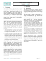
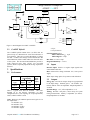
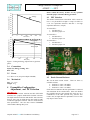
Charge Sensitive Preamplifier
A250CF CoolFET
Amptek sets the New State-of-the-Art... Again!
with Cooled FET
Performance
• Noise: 670 eV FWHM (Si)
~76 electrons RMS
• Noise Slope: 11.5 eV/pF High Ciss FET
• Fast Rise Time: 2.5 ns
Features
• Thermoelectrically Cooled FET
• 3 FETs to match detector
• Lowest Noise and Noise Slope
• AC or DC coupling to the detector
• Easy to use
• Both Energy and Timing outputs
• Optional input protection
RUN SILENT...RUN FAST...RUN COOL!
The Amptek A250CF "Cool FET" Charge Sensitive Preamplifier is the lowest noise, general purpose, preamplifier
available. It is designed to give the ultimate performance when used with either low or high detector capacitance
detectors and is a direct replacement for other higher noise charge sensitive preamplifiers.
The A250CF “CoolFET” technology uses a thermoelectric (Peltier) cooler to keep the input FET(s) at -50 °C. Cooling
is totally transparent to the user. Hence, the A250CF “CoolFET” operates like a room temperature preamplifier. Based
on the successful A250 designed for high performance satellite instrumentation, the A250CF "CoolFET" re-defines the
new state-of-the-art.
Power to the A250CF "CoolFET" is provided by an external stable power supply (included). Detector bias can be
applied via an SHV connector. Input, Energy (E) Output, Timing (T) Output, and Test are provided via BNC
connectors.
100
Noise (Si equivalent keV FWHM)
Low Ciss
High Ciss
10
1
0.1
1
10
100
1000
Detector Capacitance (pF)
Figure 2. Noise as a function of FET and detector capacitance. D.C. Coupled.
Amptek A250CF CoolFET User Manual - Preliminary
Page 1 of 7
Charge Sensitive Preamplifier
A250CF CoolFET
1
Warnings
Under normal operation, a high voltage bias is applied
across the detector that is used with the Amptek A250CF
preamplifier. The user must exercise care when the
detector is biased. Moreover, the bias circuitry has a very
long time constant and so this circuitry, including the
A250CF’s input node, can remain at a high voltage for a
very long time. If the user does not exercise suitable
caution, this voltage can possibly cause personal injury.
More likely, however, is that this voltage could damage or
destroy either the detector or the A250CF and void
warranty if proper care and operation are not exercised as
discussed in this manual.
The input circuit will be destroyed if the detector input
capacitor is shorted while the detector bias components are
charged. These capacitors retain charge for a long period of
time. A short circuit, which can result from connecting a
detector, cable, or capacitor, will cause the applied bias
voltage (stored on the input capacitor) to be coupled
directly to the input FET, causing catastrophic damage to
the FET inside the CoolFET hybrid. To avoid the
possibility of such damage, please observe the following
precautions:
1. Completely discharge the detector bias circuit by turning
off the bias supply before connecting a cable, capacitor,
or any other device to the Detector Input connection on
the front panel of the preamplifier.
2. To discharge the circuit if a variable HV supply is used,
turn the voltage control to zero and leave it there for are
least 30 seconds. The bias circuitry will discharge itself
through the output of the bias supply. Otherwise,
connect a low impedance, ideally a short circuit, across
the Detector Bias SHV connector on the rear panel of the
preamplifier for at least 30 seconds. Do not short the
Detector Input connector on the preamplifier.
The preamplifier includes a protection circuit that is
enabled when the unit ships from the factory, which
protects the input FET from destruction due to large
transients under abnormal operating conditions. It is
important to note that this circuit protects the FET and not
the detector. If the detector breaks down due to over
voltage, the protection circuit prevents damage to the
preamplifier/FET. The protection circuit does add to the
electronic noise of the preamplifier, so if the lowest noise is
required, this circuit can be removed, as described later in
this manual. However, this leaves the FET susceptible to
damage by a variety of transients. The “half life” of an
unprotected FET is much shorter than that of a protected
FET, so there is a trade-off between the very lowest noise
and risk. Damage caused during unprotected operation is
not covered under warranty unless the precautions outlined
here are followed.
Amptek A250CF CoolFET User Manual - Preliminary
2
2.1
Overview
Description
The A250CF is a charge sensitive preamplifier. The input
to the preamplifier is the signal from a radiation detector, a
current pulse of short duration (mseconds or less). The total
energy deposited is proportional to the total charge
generated.
The primary output of A250CF (the energy output) is a
voltage step proportional to the input charge, the time
integral of the current pulse, with a gain of 176 mV/MeV
(Si). This step has a fast rise (the rise time of the A250CF is
2.5 nsec for 0 capacitance) and a slow decay to baseline
(500 msec). This energy output is generally sent to a
shaping amplifier and is used for spectroscopic
measurements. The timing output has a much faster decay,
1 msec, and is used as the input to a timing circuit.
The A250CF consists of several main function blocks. The
core of the preamplifier is the charge amplifier itself, which
consists of the CoolFET hybrid, the A250 amplifier, and the
feedback components. This circuit produces the voltage
output for a current input, and determines the output noise
and risetime.
The series noise of a preamplifier is at its minimum when
the input capacitance is comparable to the FET capacitance.
The A250CF includes a jumper that permit the user to select
1 of 3 FETs, to match capacitance. Jumpers are used to
connect the gates to the input, to connect the commensurate
drains, and to select the proper drain resistor, to set the drain
current.
There are additional circuit elements in the A250CF,
including (1) connections to detector bias, (2) optional input
protection circuitry (enabled when shipped from the
factory), (3) a test input, (4) an amplifier which buffers the
energy output and provides for polarity and offset
adjustments, (5) an amplifier which buffers the timing
output and provides for polarity adjustment, and (6) power
supply circuitry.
Page 2 of 7
Charge Sensitive Preamplifier
A250CF CoolFET
Drain Current
Jumpers
Bias
SHV
Drain
Jumpers
Offset
Adjust
100 MΩ
Gate
Jumpers
Gain of 2
Optional Invert
Energy
Gain of 2
Optional Invert
Timing
A250
DC or AC Coupling
Input Protection
Jumper
Input
Thermoelectric
Cooler
49.9
CoolFET
Hybrid
Test
+/- 8V
1 GΩ
+/- 5V
Power
Supply
+3.3V
TEC Pwr
0.5
pF
Figure 1. Bock Diagram of A250CF "CoolFET."
2.2
4 V/pC
0. 64 µV/electron
CoolFET Hybrid
The CoolFET hybrid contains three (3) FETs that are
placed on top of a thermoelectric cooler and enclosed in a
TO-8 package. There are two main advantages to cooling
the FET: it reduces the leakage current and increases the
transconductance, both of which reduce the electronic noise
of the system. The increased transconductance provides a
much improved noise slope (eV/pF) over un-cooled
systems, which is especially important for large capacitance
detectors.
3
3.1
FET Capacitance (Ciss):
FET 1 and 2 Low Ciss: 15 pF
FET 3 High Ciss: 30 pF
Rise Time: 2.5 nsec at 0 pF
Integral Nonlinearity: < 0.03%
3.2
Inputs
Specifications
Detector Input: Positive or negative input signals from
semiconductor detectors.
Performance
Bias: Detector bias voltage, maximum 1 kV, from a power
supply.
Noise at 0 pF (keV)
(2 µs shaping)
CoolFET
Test: Input voltage pulses for system test and calibration.
Noise
Slope
(eV/pF)
100 MΩ
Type
DC
coupled
Low Ciss
0.670
1.20
13
High Ciss
0.850
1.35
11.5
Bias
Table 1. Typical noise data for A250CF. The noise
depends on (1) the detector capacitance, (2) input
configuration (AC vs DC coupling, use of input protection),
and (3) which CoolFET is used.
3.3
Outputs
Energy (E): Provides an output voltage step proportional
to the input charge. Nominal gain is 176 mV/MeV (Si).
Polarity and DC offset are adjustable. Output Impedance is
50 Ohms.
Dynamic Range: ± 4 V, offset adjustable to ± 6 V
Timing: Provides a tail pulse (1 msec decay) for system
timing measurements. Polarity is adjustable. (see below).
Output Impedance is 50 Ohms.
Gain: With a 0.5 pF feedback capacitor and a gain of 2 in
the output buffer.
176 mV/MeV (Si)
220 mV/MeV (Ge)
144 mV/MeV (CdTe)
152 mV/MeV (HgI2)
Amptek A250CF CoolFET User Manual - Preliminary
Page 3 of 7
Charge Sensitive Preamplifier
A250CF CoolFET
Please contact the factory if there are any questions
about the proper selection/soldering procedure.
1.0
Normalized Amplitude (V)
0.9
Energy
0.8
4.1
0.7
FET Selection
The A250CF contains three cooled FETs. FETs 1 and 2 are
low Ciss =15 pF and FET 3 is high Ciss=30 pF. Use FET 1 or
2 for low capacitance detectors and FET 3 for high
capacitance detectors (>100 pF).
0.6
0.5
0.4
0.3
To select FET 1:
1. Set JP8 to Pin 5
2. Set JP7 to jumper 1-2
0.2
0.1
0.0
Normalized Amplitude (V)
-50
0
50
100
150
Time (msec.)
1.0
0.9
0.8
0.7
0.6
0.5
0.4
0.3
0.2
0.1
0.0
200
250
To select FET 2:
1. Set JP8 to Pin 6
2. Set JP7 to jumper 3-4
To select FET 3:
1. Set JP8 to Pin 7
2. Set JP7 to jumper 7-8
Energy Output
Timing Output
0
100
200
Time (nsec.)
300
400
Figure 3. Timing and energy outputs from a typical test
pulser.
3.4
Connections
Input, Test, Energy, Timing: BNC
Bias: SHV
3.5
Power
3.3 V DC at 1.6 A (AC power adapter included)
3.6
Mechanical
Size: 3.5” x 2.5 “
Weight: 28 g
4
Preamplifier Configuration,
Adjustment, and FET Selection
IMPORTANT
JP6 (drain current resistor selection) and JP7 (FET Drain
selection) have jumpers installed that facilitate selection.
The Input Protection selection and the FET Gate selection,
however, have posts to which the user must solder in order
to make the appropriate selection. This is to ensure the best
noise performance. The user must exercise EXTREME
caution while soldering these posts.
Amptek A250CF CoolFET User Manual - Preliminary
Figure 4.
4.2
Drain Current Resistors
JP6 sets the drain current resistor. There are three (3)
selectable resistors.
• Position 1-2: R34 = 220 Ohms
• Position 3-4: R35 = 110 Ohms
• Position 5-6: R36 = 110 Ohms
Under most circumstances the best performance is achieved
with 220 Ohms for the CoolFet FETs. If the user disables
the CoolFET and uses and external FET, then one (or a
combination) of the other positions may yield the best
results. Also, at higher detector capacitances a lower value
may improve noise results.
Page 4 of 7
Charge Sensitive Preamplifier
A250CF CoolFET
4.3
AC and DC Coupling
The A250CF is shipped from the factory configured for AC
coupling with the Bias resistor and filter installed. The Bias
is connected through a teflon post to the BNC side of the
input capacitor by a wire.
To DC couple the A250CF the user must remove the
connection from this post to input capacitor and then solder
a jumper wire across the input capacitor or remove it and
make a direct connection to the input node.
4.4
Input Protection
The A250CF is shipped with the protection network
enabled (ah shown in figure 5). The best noise performance
is obtained without any protection, but the risk of damage is
much higher. Follow the precautions outlined in Section 1
when disabling the protection. The diode protection
degrades the noise performance more the higher the
dectector capacitance.
4.5
Energy Output (E)
The Output of the A250 is buffered by an amplifier with a
Gain of 2. Both the polarity and the offset of the Energy
Output (E) can be user adjusted. Output Impedance is 50
Ohms.
The DC offset of the energy output can be adjusted by using
potentiometer R9. It is “zeroed” when shipped from the
factory. If a grater dynamic range is needed in one direction
(i.e. positive or negative), the user can adjust this. For
example, if a greater positive dynamic range is needed, this
can be adjusted negative. The Energy Output (E) can be
inverted by using switch S1.
4.6
Timing Output (T)
The Timing Output (T) is buffered by an amplifier with a
gain of 2. The polarity of the timing output can be toggled
by using switch S2. Output Impedance is 50 Ohms
5
Testing via “Test” Input
The A250CF can be tested with a pulser to inject a test
charge into the Test input. The unit will respond to both the
negative and positive edge of the test pulse which should
have a transition time of less than 20 ns. A square wave or a
tail pulse with long fall time (>100 µs) may be used. Charge
transfer to the input of the A250CF is being applied only
during the transition time according to Q = CtV, where Q =
total charge transferred, Ct = value of test capacitor, and V =
amplitude of voltage step. DO NOT connect the test pulser
to the input directly or through a test capacitor greater than
100 pF as this can produce a large current pulse at the input
FET and cause irreversible damage.
Figure 5. Shows the protection network enabled. D1 is
soldered and the R5 jumper is not soldered. Refer to
shcematics at end of manual.
Input waveform: Square wave, or Tail pulse (Tr < 20ns, Tf
> 100 µs)
Amplitude: V = Q/Ct = 1 V/picoCoulomb for Ct = 1 pF
Example: To simulate 1 MeV in Si detector: 1 MeV (Si) =
0.044 pC, (1 V/pC)( 0.044 pC) = 44 mV
Hence, a 44 mV step into 1 pF test capacitor simulates the
charge generated in a silicon detector by a particle when it
loses 1 MeV of its energy.
NOTE: The internal test capacitor (0.5 pF) is not a
calibrated capacitor. It is provided to facilitate the testing of
the preamplifier and not to make absolute noise
measurements.
Figure 6. Shows the protection network disabled. D1 is not
sodlered and the R5 jumper is sodlered.
Amptek A250CF CoolFET User Manual - Preliminary
Page 5 of 7
Charge Sensitive Preamplifier
A250CF CoolFET
6 Noise Measurement
The noise of a charge sensitive preamplifier must be tested
together with the post amplifier/shaper. The A250CF noise
characteristics given in the specifications are associated
with a 2 µs shaping time constant in the post amplifier. The
post amplifier must have very low input noise as in the case
of NIM electronics amplifiers or the Amptek A275, so that
its contribution to the measurement is minimal. The
function of the post amplifier is not only to preserve and
amplify the linear information received by the charge
amplifier, but also to provide a band pass filter to eliminate
frequencies that contribute to noise.
Conversion: 1 keV FWHM (Si) = 113 electrons RMS =
1.81 x 10⁻¹⁷ Coulombs RMS
When measuring noise of the entire system either by the
MCA or the RMS voltmeter method the detector must be
simultaneously connected with the test circuit to the input of
the A250CF. The noise measurement in this case will
include the contribution from the detector due to both its
capacitance and its leakage current.
Two methods are normally used to measure noise in the
preamplifier: The first is by using a Multichannel Analyzer
(MCA), and the second is with a wide-bandwidth RMS AC
voltmeter.
6.1 Noise Measurement Using an MCA
Connect a calibrated capacitor (1-2 pF, not provided) to the
Input of the A250CF. Stimulate with a pulse of known
amplitude as in the Section 5.
1. Connect the A250CF Energy Outpu (E) to the post
amplifier/shaper with the correct shaping time constant
(1-3 µs for solid state detectors.)
2. Connect the post amplifier output to the MCA input.
3. Calibrate the MCA, in pC/channel or keV/channel, by
observing two peaks formed by two different known
amplitude test pulses.
4. The Full Width at Half Maximum (FWHM) of a
particular energy peak can now be read directly from the
analyzer.
6.2 Noise Measurement Using RMS Voltmeter
Connect a calibrated capacitor (1-2 pF, not provided) to the
Input of the A250CF. Stimulate with a pulse of known
amplitude as in the Section 5. The FWHM noise using the
RMS voltmeter is given by:
FWHM (keV, Si) = 2.35 (Vrms) (Vin)/(Vout)
Where:
• Vrms is the noise in volts from the voltmeter.
• Vin is the input test pulse in keV equivalent.
• Vout is the output pulse in volts from the post
amplifier.
Example: With a 2 pF test capacitor
1. Set Vin = 22 mV (1 MeV, Si)
2. Set Post amplifier's gain to obtain 2.35 Volts output
pulse
3. The RMS voltmeter is now calibrated to:
1 mV RMS = 1 keV FWHM (Si)
4. Remove the test pulser, cover the input BNC, and read
the RMS voltmeter.
Amptek A250CF CoolFET User Manual - Preliminary
Page 6 of 7
Charge Sensitive Preamplifier
A250CF CoolFET
7
Schematic
Amptek A250CF CoolFET User Manual - Preliminary
Page 7 of 7