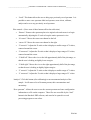
1
Approved for public release; distribution is unlimited.
Borehole X-Ray Fluorescence Spectrometer (XRFS):
User's Manual, Software Description,
and Performance Report
built by APL-UW under a NASA contract from the Langley Research Center
W.C. Kelliher1, I.A. Carlberg1, W.T. Elam2, and E. Willard-Schmoe2
1NASA Langley Research Center, Hampton, VA
2Applied Physics Laboratory, University of Washington, Seattle
Technical Report
CAUTION CAUTION CAUTION
APL-UW TR 0703
December 2007
This device produces
X-rays when energized.
CAUTION CAUTION CAUTION
Applied Physics Laboratory University of Washington
1013 NE 40th Street
Seattle, Washington 98105-6698
Contract NNL05AA49C
_______________________UNIVERSITY OF WASHINGTON • APPLIED PHYSICS LABORATORY_________________
Acknowledgments
This project was funded by NASA Headquarters as part of the Mars Technology
Program, Subsurface Access Task, administered by the Jet Propulsion Laboratory. We
are indebted to the program managers, Suparna Mukherjee and Chester Chu, for their
guidance. The XRF spectrometer design and construction were performed by the Ocean
Engineering Department of the Applied Physics Laboratory: Russ Light, Vern Miller,
Pete Sabin, Fran Olson, Tim Wen, and Dan Stearns. The performance reported here is
due to their efforts. The University of Washington effort was funded under NASA
contract NNL05AA49C.
i
TR 0703
_______________________UNIVERSITY OF WASHINGTON • APPLIED PHYSICS LABORATORY_________________
TR 0703
ii
_______________________UNIVERSITY OF WASHINGTON • APPLIED PHYSICS LABORATORY_________________
Contents
User’s Manual ...............................................................................................................1
Overview.....................................................................................................................1
Borehole XRFS Software Installation ........................................................................12
Instrument Design .....................................................................................................15
Typical Operation......................................................................................................19
Determining the Minimum Detection Limit (MDL) ...................................................40
Hardware Description.................................................................................................23
XRF Interface Unit....................................................................................................23
XRF Control Unit......................................................................................................26
Software Description ...................................................................................................29
X-ray Tube Control (XTC) ........................................................................................29
Detector Data Acquisition (DET) ..............................................................................31
Save and Load Parameters (PAR)..............................................................................33
Save and Load Spectrum (SSF) .................................................................................34
Spectrum Processing (SP)..........................................................................................36
Spectrum Display (SD)..............................................................................................36
Instrument Performance Report ................................................................................38
Materials and Methods ..............................................................................................39
Test Plan Summary....................................................................................................41
Results.......................................................................................................................42
Conclusions...............................................................................................................52
Appendices...................................................................................................................53
iii
TR 0703
_______________________UNIVERSITY OF WASHINGTON • APPLIED PHYSICS LABORATORY_________________
TR 0703
iv
_______________________UNIVERSITY OF WASHINGTON • APPLIED PHYSICS LABORATORY_________________
User’s Manual
Overview
The X-ray fluorescence spectrometer (XRFS) is designed to be deployed down a predrilled hole for exploration and elemental analysis of subsurface planetary regolith
(Figure 2 and Figure 10). The spectrometer excites atoms in the regolith and causes them
to emit their characteristic X-rays. These characteristic X-rays produce peaks in the Xray spectrum. By measuring the energy of the X-rays, elements are identified. By
measuring the intensity of the peaks, the amount of each element can be determined. A
software package operates the spectrometer, acquires the data, and analyzes the spectrum
to provide elements and their weight fractions. It also provides a user interface to control
the measurements and display the results.
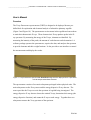
Figure 1. X-ray fluorescence spectrometer Head Unit designed to be deployed down a pre-drilled
hole to analyze subsurface elements.
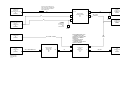
The spectrometer consists of two main subsystems packaged in three physical units. The
main subsystems are the X-ray source and the energy-dispersive X-ray detector. The
source provides the X-rays to excite the specimen of regolith being investigated. The
energy-dispersive X-ray detector detects the emitted X-rays, determines their energy (the
energy-dispersive function), and counts the X-rays at each energy. Together these two
subsystems measure the X-ray spectrum of the specimen.
1
TR 0703
_______________________UNIVERSITY OF WASHINGTON • APPLIED PHYSICS LABORATORY_________________
Quick Start Guide
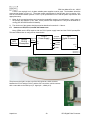
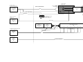
Figure 2. (from left to right) Borehole XRFS Head Unit, X-ray warning light, umbilical cable, X-ray
Interface and Control units, and laptop computer.
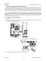
Setup
To set up the instrument:
1. Remove the units from the case. The instrument consists of the XRF Interface
Unit, the XRF Control Unit, and the XRF Head Unit (Figure 2). A laptop
computer is used to control the instrument. There are three cables connecting the
Interface and Control units, and the Head Unit has an umbilical cable (15 ft.
long) permanently attached to connect it to the Control Unit. An X-ray warning
light is also supplied. The instrument must be used in a radiation safety enclosure
TR 0703
2
_______________________UNIVERSITY OF WASHINGTON • APPLIED PHYSICS LABORATORY_________________
or other personnel safety arrangement. An interlock cable connects to the safety
interlock switch on the radiation safety enclosure to prevent accidental exposure.
2. Connect the cables as shown in Figure 3. All cables must be connected before
turning on the main power.
3. Connect USB cable to the laptop computer and turn on the instrument with the
key switch. The laptop should beep when it recognizes the connection to the
instrument.
4. Wait one to two minutes for the detector to cool down. The instrument is now
ready to collect a spectrum.
3
TR 0703
_______________________UNIVERSITY OF WASHINGTON • APPLIED PHYSICS LABORATORY_________________
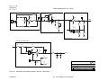
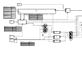
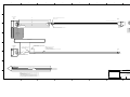
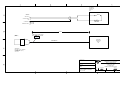
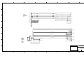
Figure 3. Connection diagrams for Interface, Control, and Head units of the XRF spectrometer.
TR 0703
4
_______________________UNIVERSITY OF WASHINGTON • APPLIED PHYSICS LABORATORY_________________
Spectrum collection
1. Place the sample to be analyzed before the probe window.
2. Close the radiation safety enclosure and be sure the interlock switch is closed.
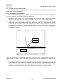
3. Start the program “BoreholeXRF”; the main screen appears (Figure 4).
4. Turn on the high voltage to 35 kV, and the emission current to 2 µA.
5. Set the preset time to the desired interval.
6. Click “Start”.
7. The actual kV and µA values should be near the setting values (they may take one
or two minutes to reach these values because of the slow ramp).
8. “Acquiring” will appear in red on the screen (Figure 5).
9. A spectrum will begin to appear in the plot box in the lower left corner of the
interface (Figure 5).
10. To calibrate, click “Calibrate” and enter points in the form “channel number,
energy in keV” in the window that opens (Figure 6). Then click “Compute,” then
“Calibrate,” then “Close.” You may calibrate before, during, or after spectrum
collection.
11. To save the spectrum, click “Save.”
12. To determine which elements are present in the sample, click the “Analyze”
button. After several seconds, the plot box will show the background and
spectrum fits and the elemental analysis will appear in the spectrum analysis box
(Figure 7).
Software operation
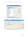
Configuration settings:
•
“load params panel” (Figure 8): Opening this window allows the user to change
instrument control parameters (such as the ramp interval) and acquisition
conditions (such as the atmosphere type).
5
TR 0703
_______________________UNIVERSITY OF WASHINGTON • APPLIED PHYSICS LABORATORY_________________
•
“load DP4 config panel” (Figure 9): Opening this panel allows the setting for the
DP4 digital pulse processor to be changed. Refer to the AmpTek manual
(Appendix A) on the DP4 for more information about these parameters.
•
“on” and “off” under “X-ray control”: These buttons turn the X-rays on and off.
•
“setkV”: This button allows the user to set the high voltage for the X-ray tube.
•
“set µA”: This button allows the user to set the emission current.
•
“change preset time”: Use this button to enter the desired interval of data
collection in seconds, then click “OK.” This command automatically clears the
spectrum that is currently plotted (so save it first!). When the user clicks “Start”
after entering this preset time, the program will collect a spectrum and stop
automatically after the allotted time has elapsed. Note that this refers to
accumulation time, not live time.
“Input Spectrum” functions:
•
“Start”: Click this button to begin taking a spectrum.
•
“Stop”: Click this button to stop spectrum collection before the preset time has
elapsed.
•
“Clear”: This button clears the spectrum currently plotted.
•
“Calibrate”: The user may calibrate the energy of the spectrum any time before,
during, or after collection. It is also possible to load and calibrate a previously
saved spectrum. Click “Calibrate” to open the calibration window, enter the
desired channel-energy pairs (in keV) in the form “channel, energy,” click
“Compute,” “Calibrate,” and “Close.” It is also possible to type a desired energyper-channel value and energy start value manually and then click “Calibrate,”
without pressing “Compute.” The user may clear a previous calibration and
return to the original channel values by pressing “Remove calibration.”
TR 0703
6
_______________________UNIVERSITY OF WASHINGTON • APPLIED PHYSICS LABORATORY_________________
•
“Load”: This button allows the user to bring up a previously saved spectrum. It is
possible to enter a new spectrum label and operator, zoom in/out, calibrate,
analyze and re-save any previously saved spectrum.
Plot controls: (Note: none of these buttons affect data collection.)
•
“Restore”: Restores the spectrum plot to its original scale and causes it to begin
automatically adjusting the Y-scale to keep the entire spectrum in view.
•
“ cursor”: Moves the cursor one channel to the left.
•
“cursor ”: Moves the cursor one channel to the right.
•
“X zoom in”: Adjusts the X-scale so that it displays a smaller range of X values,
centered around the cursor.
•
“X zoom out”: Adjusts the X-scale so that it displays a larger range of X values,
centered around the cursor.
•
“X shift left”: Moves the view to the left approximately half of the plot range, so
that the user is looking at slightly lower energies.
•
“X shift right”: Moves the view to the right approximately half of the plot range,
so that the user is looking at slightly higher energies.
•
“Y zoom in”: Adjusts the Y-scale so that it displays a smaller range of Y values.
•
“Y zoom out”: Adjusts the Y-scale so that it displays a larger range of Y values.
“Analyze”: Click this button (after calibrating) to run an automated analysis of the
sample. It will return a list of elements present, their concentrations and
uncertainty.
“Save spectrum”: Allows the user to save the current spectrum and some configuration
information to a file on the computer. These files are accessible by the “load”
button in the Borehole XRF software, and can also be opened in a word
processing program or text editor.
7
TR 0703
_______________________UNIVERSITY OF WASHINGTON • APPLIED PHYSICS LABORATORY_________________
“Exit”: Exits the spectrum collection program. The program will not prompt the user to
save the current spectrum, so it is necessary to save (if desired) before exiting.
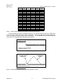
Figure 4. Main screen view upon starting the program “BoreholeXRF”
TR 0703
8
_______________________UNIVERSITY OF WASHINGTON • APPLIED PHYSICS LABORATORY_________________
Figure 5. View of laptop display during spectrum acquisition
Figure 6. View of calibration control window
9
TR 0703
_______________________UNIVERSITY OF WASHINGTON • APPLIED PHYSICS LABORATORY_________________
Figure 7. View of spectrum analysis display
TR 0703
10
_______________________UNIVERSITY OF WASHINGTON • APPLIED PHYSICS LABORATORY_________________
Figure 8. View of configuration setting “load parameters panel”
Figure 9. View of configuration setting “load DP4 configuration panel”
11
TR 0703
_______________________UNIVERSITY OF WASHINGTON • APPLIED PHYSICS LABORATORY_________________
Borehole XRFS Software Installation
Before connecting hardware, copy all files from CD-R folder titled “BoreholeXRF As
Shipped Bin Sept 27.2007.”
Place files in C:\Program Files\BoreholeXRF
(Note: the files MUST be in exactly this location to operate correctly.)
Necessary software files from the folder “BoreholeXRF As Shipped Bin Sept 27.2007”:
•
xrayxsct.dat
•
XRFanalysis.dll
•
APL_UW_XraySettings.xcg
•
asycfilt.dll
•
BoreholeXRF.exe
•
cbw32.dll
•
COMCAT.DLL
•
COMCT232.OCX
•
Comdlg32.ocx
•
dp4.cfg
•
MSCOMM32.OCX
•
msvbvm60.dll
•
oleaut32.dll
•
olepro32.dll
•
usbdrvd.dll
Install the driver for the Measurement Computing DAQ module.
•
Load the Measurement Computing “MCC DAQ Software” CD
•
Install InstaCal for Windows, TracerDAQ, and Hadware manuals
•
Install Shield Wizard for InstaCal – click “Next”
•
Destination Folder – click “Next”
TR 0703
12
_______________________UNIVERSITY OF WASHINGTON • APPLIED PHYSICS LABORATORY_________________
•
Ready to Install – click “Install”
•
Completed – click “Finish”
•
Install Shield Wizard for TracerDAQ – click “Next”
•
Destination Folder – click “Next”
•
Ready to Install – click “Install”
•
Completed – click “Finish”
•
User's Guides Setup – select “USB,” then click “Install”
(Driver is installed. This takes a few seconds.)
•
MCC DAQ message box – “You must restart your system...” – click “Yes”
After system has restarted, connect Borehole XRF hardware to USB port and turn power
on. “Found New Hardware Wizard” should appear.
“Can Windows connect to Windows Update...” – choose “No, not at this time.” – click
“Next”
Install software for DP4 Digital Pulse Processor (see also page 19 of Appendix A)
•
Select “Install from a list or specific location” – click “Next”
•
Select “Don't search, I will choose the driver to install” – click “Next”
•
Hardware type – Select “Human Interface Devices” – click “Next”
•
“Select the device driver...” – Click “Have disk...”
•
Insert the AmpTek CD into the CD drive
•
Click “Browse...”
•
“Install From Disk” file dialog appears
•
Navigate in the file dialog to:
My Computer\AMPTEK\USB_Driver\Win2k_XP\apausb2k.ini
•
Click “Open”
•
Back at the “Install From Disk” dialog – click “OK”
•
Back to “Select the device driver...” dialog – click “Next”
(Driver is installed. This takes a few seconds.)
13
TR 0703
_______________________UNIVERSITY OF WASHINGTON • APPLIED PHYSICS LABORATORY_________________
•
Completing installation – click “Finish”
Run the InstaCal program
•
From the menu bar, select: Start -> Programs -> Measurement Computing ->
Instacal
•
“Plug and Play Board Detection, USB-1408FS (Serial# 150)” should be selected
•
Click “OK”
•
Under the Install menu item, choose “Configure...”
•
Change No. of Channels from “4 Differential” to “8 Single Ended”
•
Click “OK”
•
Under the File menu item, choose “Exit”
Run the Borehole XRF program by double-clicking on the file “Borehole XRF.exe”
At this point the software main screen should appear; it will obtain a spectrum and bring
up all dialogs.
You may want to put a shortcut to the “Borehole XRF.exe” file on the desktop or some
other convenient location.
TR 0703
14
_______________________UNIVERSITY OF WASHINGTON • APPLIED PHYSICS LABORATORY_________________
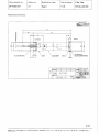
Instrument Design
The instrument is designed to be deployed down a pre-drilled borehole and has a
maximum diameter of 27.1 mm to be compatible with existing drills (Figure 1 and Figure
10). The XRFS sensor assembly consists of an XRFS enclosed head assembly that is
deployed down the borehole and an electronics control assembly consisting of a power
supply and control electronics for the XRFS instrument. PC-based software provides the
control, data readout, and quantitative calculations needed for interpretation of the XRFS
spectra.
The excitation source is a silver anode X-ray tube (Comet NA, Stamford, CT) [see
Appendix B]. The energy dispersive X-ray detector is a 7-mm2 Si–PIN diode (Amptek,
Inc., Bedford, MA) [see Appendix C]. This detector was chosen mainly because of the
availability of a preamplifier compatible with the size restrictions. It has a good peak to
background ratio and a 12-micron thick beryllium window for light element sensitivity. A
digital pulse processor from the detector manufacturer (Amptek, Inc., Bedford, MA)
converts the detector output to an energy spectrum [see Appendix C]. The energy
calibration is linear and determined from the location of the iron characteristic emission
and silver elastic scatter peaks. Because the borehole diameter cannot be controlled with
precision, the collimation and beam definition geometry are optimized to allow for
varying distance to the measurement volume at the borehole wall. The excitation beam is
larger than the area viewed by the detector, making the signal less sensitive to the wall
distance.
The performance requirement is to detect the elements magnesium through zirconium
(atomic numbers 12 through 40 in the periodic table) and the elements cadmium through
15
TR 0703
_______________________UNIVERSITY OF WASHINGTON • APPLIED PHYSICS LABORATORY_________________
lead (atomic numbers 48 through 82 in the periodic table).
Figure 10. Engineering drawing of the final design of the downhole assembly. The enlarged area
shows the X-ray tube and the detector.
Major hardware subsystems
The X-ray source is a miniature but otherwise conventional X-ray tube. It generates Xrays by bombarding a metal anode with high-energy electrons. The electrons are
TR 0703
16
_______________________UNIVERSITY OF WASHINGTON • APPLIED PHYSICS LABORATORY_________________
produced in a hot filament and accelerated to high energy by a high voltage. The
filament heater power controls the beam, or emission, current. The X-ray output is
proportional to this current. The electron beam energy is controlled by the high voltage
applied to the X-ray tube. This voltage determines the X-ray spectrum emitted by the
tube and is one of the main parameters used to control the spectrometer. The X-ray tube
has a very high vacuum inside and the X-rays exit via a thin window. Other parameters
that influence the X-ray spectrum of the tube are the angles that the electron beam makes
with the anode and the exit window, the material and thickness of the exit window, and,
of course, the anode material.
The X-ray detector is based on a silicon diode that is reverse biased to provide a thick
region of high-resistivity silicon with an electric field across it. The X-rays are absorbed
in this region and produce electron–hole pairs in the silicon. The high electric field
separates the electron–hole pairs and produces a pulse of charge at the electrodes of the
diode. This pulse is amplified and its amplitude measured. Its amplitude is proportional
to the energy of the absorbed X-ray. A digital pulse processor separates this pulse from
the noise, determines its amplitude, digitizes the amplitude, and counts the pulses with
matching amplitudes to collect a spectrum.
The silicon diode is taken to about –60ºC by Peletier cooling to reduce the noise and
allow better resolution of the pulse amplitude. The energy resolution in the spectrum is
limited by the electronic noise in the diode and is typically about 150 electron volts. The
digital pulse processor is optimized for detecting and discriminating X-ray pulses from
this diode from the background noise. The count rate (the maximum rate that X-rays can
strike the detector) is limited to about 10,000 per second by the speed of the pulse
processing. The count rate is determined by the material being measured and the strength
of the X-ray source. The rate is typically adjusted by controlling the beam current in the
X-ray tube, as described above.
17
TR 0703
_______________________UNIVERSITY OF WASHINGTON • APPLIED PHYSICS LABORATORY_________________
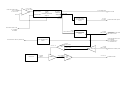
Hardware physical units
The subsystems are packaged into three units: the XRF Head that goes down the
borehole and makes contact with the material being measured, the XRF Control Unit,
and the XRF Interface Unit.
The X-ray Head contains the X-ray tube and the silicon diode X-ray detector. It also has
a filament isolation transformer for the X-ray tube to isolate the filament heating power
from the high voltage. It contains a preamplifier for the detector to amplify the pulses
before they travel over the connecting cable. The X-ray Head is as small as possible to
go down the smallest pre-drilled hole and measure the composition of the regolith at
various depths. The 15-ft. umbilical cable is permanently attached to the Head Unit; it
connects the Head and Control units.
The XRF Control Unit contains all of the essential electronics to operate the X-ray tube
and detector. It constitutes the electronics that would be required for a future spacecraft
instrument. For the X-ray tube, there is the high voltage power supply (HVPS), the
filament driver and regulator, isolation amplifiers to provide monitor signals for the
voltage and current, and an over-current protection circuit. For the detector, the unit
contains a power supply board and the digital pulse processor board.
The XRF Interface Unit contains the hardware necessary to adjust and monitor the Xray tube voltage and current from the host computer, several interlock sensors for
personnel safety, and the low voltage power supplies for the electronics. This unit
contains all of the support equipment that is necessary to operate the spectrometer on the
ground. There are several cables connecting the XRF Interface and XRF Control units.
The XRF Interface Unit also connects to the host computer via USB, to the personnel
safety outerlocks, and to the main power line.
TR 0703
18
_______________________UNIVERSITY OF WASHINGTON • APPLIED PHYSICS LABORATORY_________________
The software described here interacts mainly with the data acquisition board used to
control the X-ray tube high voltage supply and with the digital pulse processor board for
the detector. These functions are described more fully beginning on page 26.
Typical Operation
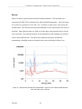
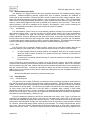
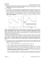
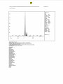
A typical X-ray spectrum of terrestrial soil is shown in Figure 11. There are three
significant features. First are the large peaks in the spectrum between 3 and about 15
keV. These peaks are from the elements in the sample and are the main features of
interest. Second are the peaks between 15 and 20 keV. These are the characteristic peaks
from the X-ray tube anode material (silver in this case) that have been scattered toward
the detector by the sample. They can provide additional information but are not as
straightforward to interpret. The third feature is the background under the peaks. The
background is small in an XRF spectrum from a good spectrometer, allowing detection of
even very small peaks from elements at very low concentrations (the minimum detection
limit). However, it must be modeled and removed by the analysis algorithms to provide
accurate measurements of the peak intensities.
19
TR 0703
_______________________UNIVERSITY OF WASHINGTON • APPLIED PHYSICS LABORATORY_________________
Figure 11. Fluorescence spectrum taken with the borehole XRFS. The soil sample was JSC1A
Lunar Simulant.
Typical operation of the spectrometer by a user involves these steps. When power is
turned on, the X-ray source is off (not producing X-rays) and the detector starts to cool
down. The user places a specimen in front of the measurement window on the side of the
XRF head (or places the head in a borehole).
The user then closes a radiation safety enclosure. When the safety enclosure is closed, a
safety interlock switch closes, allowing the X-rays to be turned on. The voltage and
current for the X-ray tube are set at this time, or previous settings are read in and used.
The user chooses a data acquisition time, clears the spectrum in the digital pulse
processor (DPP), and starts data acquisition. The spectrum is displayed as it is collected
and the user will typically check the total count rate and make sure the spectrum looks
correct (perhaps examining some regions more closely using zoom and pan). The user
may be looking for particular elements, and will thus focus on the chosen elements. The
TR 0703
20
_______________________UNIVERSITY OF WASHINGTON • APPLIED PHYSICS LABORATORY_________________
user will then stop the data acquisition, change any data acquisition parameters to
optimize the spectrum, clear the spectrum, and collect the desired data.
The data are displayed as a function of the X-ray energy. To do this, the detector pulse
height must be calibrated to match the X-ray energies. This is typically done using X-ray
peaks from known elements. The calibration must be checked (typically daily) and may
need to be repeated at irregular intervals.
Once data are collected, they can be stored in a file and/or analyzed further. Further
analysis consists of modeling the background, finding any peaks in the spectrum and
associating them with the corresponding elements, determining the net intensity of the
peaks, and converting this net intensity into weight fractions of the elements. The
background and a reconstruction of the spectrum using the extracted net intensities are
displayed. This allows the user to quickly and visually evaluate the analysis of the
spectrum. The element list and weight fraction of each element, together with estimated
uncertainties, are also displayed.
The conversion from peak intensity to weight fraction is accomplished using a physical
model of the interaction of X-rays with the material being analyzed. This model requires
a complete description of the instrument to give accurate results. This description is
more information than is typically changed by the user, such as fixed angles and
distances within the components. It is also more information than the software needs to
control the instrument. This information is read in from a parameter file and is usually
not changed. It can be initially entered and changed via second-level dialogs that are
invisible unless needed.
The user can also enter information about the material being analyzed and can change the
instrument description information to be stored with the spectrum if desired. The data
21
TR 0703
_______________________UNIVERSITY OF WASHINGTON • APPLIED PHYSICS LABORATORY_________________
acquisition parameters, such at X-ray tube voltage and current, are automatically stored
with the spectrum.
The spectrum is stored in a file along with the information about the parameters under
which it was acquired and enough of a description of the instrument to allow later
analysis if necessary. The file format used is the standard format for energy-dispersive
spectra adopted by the Microscopy Society of America and the European Microscopy
Society.1 Additional keywords were added to provide a complete description of the
measurement conditions including instrument configuration (see Table 1).
1
European Microscopy Society standard format, Version 1.0, see files emmff.doc and emmff.src,
at http://www.amc.anl.gov/ANLSoftwareLibrary/02-MMSLib/XEDS/EMMFF/
There is a proposed format based on XML that is not yet standard. See file
EMSA_MAS_V2_XML_MM8_2002.pdf
TR 0703
22
_______________________UNIVERSITY OF WASHINGTON • APPLIED PHYSICS LABORATORY_________________
Hardware Description
XRF Interface Unit
Low voltage power supplies (COTS)
+/– 15 VDC for op-amps
+15 VDC, 1.5 amp for HV module
+5 VDC for interlocks and detector
Detector requires 0.5-A steady-state with 1-A startup surge lasting 30–60 sec.
DAQ and control board (COTS)
OnTrak ADR2000A
USB to serial adaptor (COTS)
Targus PA088
USB hub (COTS)
D-Link, Model DUB-H4, high-speed USB 2.0 4-port hub
Safety interlocks and control (APL-UW)
X-ray on/off
Purpose. Turns the X-ray tube on and off, including ramping filament up and
down and safety disabling the high voltage module.
Background. This signal controls the main functions of the X-ray tube power
supply system. It is disabled whenever one of the safety signals (see below) is
absent. It will shut down and latch in the “off” condition whenever one of the
safety signals disappears.
Operation. Logic circuit responds to a binary signal from the DAQ, tests all of
the safety condition signals, and provides signals for HV disable, filament voltage
ramp control, and status to the DAQ board.
23
TR 0703
_______________________UNIVERSITY OF WASHINGTON • APPLIED PHYSICS LABORATORY_________________
Warning light and fail-safe
Purpose. Controls the warning light (115 V AC external lamp), turning it on and
off with the X-rays. Provides a safety signal that indicates when the lamp is
working.
Background. One of the federal safety requirements for X-ray systems is a
warning light that turns on whenever the X-ray producing system is energized
(defined as high voltage on). The light must be fail-safe in that the X-rays will
not come on if the light bulb is burned out.
Operation. Solid-state relay to turn the power to the external socket on and off.
A current detector (full-wave bridge rectifier in parallel with Zener diodes driving
a 5-V DC relay) indicates that the external lamp is drawing current (i.e.,
connected and not burned out). The current detector does not provide a signal
unless the lamp is energized, a delay must be provided that allows the lamp to be
turned on, then X-rays must be turned off if the current detector does not indicate
lamp operation. The delay is typically about 100 milliseconds.
Electrical interlock status
Purpose. An external signal provided by a user that indicates that all of the X-ray
shielding is in place.
Background. Another federal safety requirement is that the enclosure that
protects human operators from radiation exposure be interlocked to the high
voltage supply. This interlock must disable the high voltage if the shielding is
opened, to prevent accidental radiation exposure.
TR 0703
24
_______________________UNIVERSITY OF WASHINGTON • APPLIED PHYSICS LABORATORY_________________
Operation. An external signal. It disables the high voltage power supply and
prevent X-rays from being turned on (or shut them off if they are on). The signal
is typically an external switch closure. It also disables the X-rays in case of a
short to ground to prevent shorts from giving a false OK signal. A TTL or other
logic signal is OK if +5 V or similar is available on the external connector to
facilitate use with un-powered mechanical switches on a radiation enclosure.
Filament connector engaged
Purpose. To insure that the filament connector is inserted before the high voltage
or X-rays are turned on.
Background. The commercial, miniature high voltage connectors used have only
a contact for the negative high voltage, not for the positive return path (ground in
this case). The ground return path is via the filament connector. If the high
voltage is energized with the high voltage connector in place and the filament
connector dangling, then a shock hazard condition can be produced.
Operation: A simple logic circuit that passes through the external filament
connector via two extra pins.
Over-current signal
Purpose: See over-current cutoff under high voltage power supply board in the
XRF Control Unit above. This signal is passed through to the DAQ and should
remain after the X-rays are turned off until reset via the DAQ (usually by the Xrays off signal).
Background. This is just an interface to the over-current cutoff from the high
voltage power supply board.
25
TR 0703
_______________________UNIVERSITY OF WASHINGTON • APPLIED PHYSICS LABORATORY_________________
Operation. Logic circuit that is part of the X-ray on circuit.
Ground failure detect
Purpose. Insures that a safe return path for the high voltage exists and avoids
potential shock hazards.
Background. If high voltage is applied to the X-ray tube and a connection
between the X-ray tube anode and the return current path to the power supply
ground fails, then a potential shock hazard exists. This circuit tests the ground
return path by applying a voltage to the X-ray tube anode via a resistor, then
testing to be sure that voltage is shorted to ground.
Operation. Applies a voltage through a pair of resistors, to the X-ray tube anode
over the umbilical cable. One resistor is in the power supply and one is in the
XRF Head Unit near the X-ray tube anode. This will produce a known voltage if
the X-ray tube is properly grounded. If the umbilical cable lead is shorted, then
the voltage will be zero. Provides a signal if the correct voltage is present, and
disable the X-rays if not.
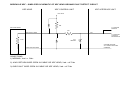
XRF Control Unit
High voltage power supply board
HV module (COTS)
Filament driver and regulator (APL-UW)
Purpose. Provides AC drive voltage for filament isolation transformer to heat
filament. Regulates filament voltage to achieve emission current set point.
TR 0703
26
_______________________UNIVERSITY OF WASHINGTON • APPLIED PHYSICS LABORATORY_________________
Background. The electron beam in an X-ray tube is generated from a hot
filament at high negative voltage. The electrons emitted from the hot filament are
accelerated by the high voltage and strike a metal anode at ground potential. The
metal anode emits X-rays. The filament is heated by a current passing through
the filament wire. Since the filament is at high negative potential, the heater
current must be isolated by a filament transformer operating at 6 kHz. The
electron beam current is regulated by the temperature of the filament, which is
controlled by the filament heater current.
Operation. 6-kHz AC is generated by an oscillator, whose output voltage is
controlled by a feedback loop. The output goes to a power audio amplifier chip to
produce enough power and voltage to drive the filament transformer (which is
located in the XRF Head). The feedback loop compares the current signal from
the HV module to a set point and adjusts the filament heater voltage. The
feedback has upper and lower limits (via a Zener diode), integration of the error
signal (via a capacitor), and some linear gain for stability (via a resistor), all in the
feedback leg of an op-amp. This regulator reverts to the “filament off” condition
on power-up and wherever X-rays are turned off.
Isolation and amplification of HV monitor signal (APL-UW)
Purpose. To condition the signals from the HV module to achieve convenient
gain and to protect the remainder of the circuits from spikes due to high voltage
arcs.
Operation. Op-amps with diode and capacitor spike suppression at their inputs.
27
TR 0703
_______________________UNIVERSITY OF WASHINGTON • APPLIED PHYSICS LABORATORY_________________
Over-current cutoff (APL-UW)
Purpose. To protect all of the hardware from a long-term overload condition.
Background. X-ray tubes sometimes develop arcs or plasma discharges. If they
are brief, they usually clear themselves and are not a problem. But if they last for
several seconds, they can overheat themselves or other components. This
protection circuit serves as a backup to the software over-current protection. The
HV module is also current-limited, but that only protects the module, not the Xray tube.
Operation. Compares the emission current signal from the HV module to an onboard set point. If the emission current exceeds the set point for more than 5 sec,
turn off the X-rays.
Detector power board (COTS)
AmpTek PC4-3
Detector pulse processor board (COTS)
AmpTek DP4. The detector system is completely isolated as well as electrically
and magnetically shielded from the X-ray tube power supply, with one common
ground point at the +5 volt power supply. The signals from the X-ray detector at
the preamp output are pulses of about 10 microseconds duration and about 1 mV
amplitude. Their amplitude must be measured to within a few percent to obtain a
useable X-ray spectrum. Electronic noise is the major limitation and is
minimized. Magnetic shielding is accomplished with co-netic foil.
TR 0703
28
_______________________UNIVERSITY OF WASHINGTON • APPLIED PHYSICS LABORATORY_________________
Software Description
X-ray Tube Control (XTC)
Description
This module has two main purposes: to display and allow the user to change the
parameters related to the X-ray tube, and to control the high-voltage power supply
(HVPS) for the X-ray tube. The controls for this module are located on the main screen
in the upper right corner of the interface (Figure 4).
The main parameters for the X-ray tube are the high voltage (kV) and the beam emission
current (µA). Typical values are 35 kV and 2 µA. The user must also input a complete
description of the X-ray tube for proper operation of the quantitative analysis software.
These parameters are in a separate dialog that appears on request but is usually invisible
(Figure 8).
The HVPS has a series of safety interlocks to prevent accidental exposure of personnel to
high electrical voltages and X-ray radiation. The status of these interlocks is clearly
visible to the user and turn red if any fail (Figure 12).
Control of the HVPS requires turning the X-ray on and off under user control, and
responding to any changes in the interlock status by turning off the X-rays. The X-ray
tube voltage and current settings are converted from the display units (kV and µA) to the
DAC integer values and sent to the DAC using its commands. The actual values are read
from the DAC and converted to the display units. When the X-rays are turned on, the Xray tube must be ramped up to the operating conditions gradually (see ramp-up under
functions).
29
TR 0703
_______________________UNIVERSITY OF WASHINGTON • APPLIED PHYSICS LABORATORY_________________
Figure 12. Borehole XRF interface indicating interlock failure
Functions
Set and display X-ray tube voltage (kV)
Set and display X-ray tube emission current (µA)
Check limits for X-ray tube parameters
Check and display status of safety interlocks
•
X-ray on/off
•
Warning light and fail-safe
•
Electrical interlock
•
Filament connector engaged
•
Over-current signal
•
Ground failure detect
Turn X-rays on and off
TR 0703
30
_______________________UNIVERSITY OF WASHINGTON • APPLIED PHYSICS LABORATORY_________________
Ramp-up X-ray tube gradually to full operation
•
Bring up kV to no more than 10 kV
•
Bring up emission current to no more than 5 µA
•
Raise kV and µA gradually together to specified values
Communicate with HVPS
•
USB port or other communication parameters
•
Commands to ADC and DAC
•
ADC and DAC conversion constants
Set and display X-ray tube and instrument description
•
X-ray tube type (side or end window)
•
Anode material
•
Be window thickness
•
Electron incident angle
•
Takeoff angle
•
Aperture size and distance
•
Filter material and thickness (if any)
•
Path length from X-ray tube to specimen
•
Angle that X-rays from tube strike specimen (incidence angle)
Detector Data Acquisition (DET)
Description
The X-ray detector acquires the spectrum; its associated electronics are commercial offthe-shelf. The manufacturer (Amptek, Inc., Bedford, MA) also supplies a library of
communications and control routines that operate over a USB interface. The main
function of the DET module is to drive these functions to acquire the spectrum (once the
X-ray tube is operating and the user requests data be collected). As with the X-ray tube,
31
TR 0703
_______________________UNIVERSITY OF WASHINGTON • APPLIED PHYSICS LABORATORY_________________
there are several data acquisition parameters that the user can change. Some of these
appear on the main screen and some in a separate dialog (Figure 9).
The signal from the X-ray detector is analyzed by a digital pulse processor (DPP) that is
specialized for energy-dispersive X-ray detector pulses. Many of the parameters for this
DPP are software changeable but require specialized commands and some tuning
procedures. The parameters are loaded at startup from a database.
One of the auxiliary functions of the detector data acquisition module is to check, set, and
maintain the detector energy calibration (Figure 6). This calibration relates the channels
in the spectrum (which are proportional to the pulse amplitude from the detector) to Xray energy. The calibration is determined using the peaks of known elements, either in
the spectrum from the material of interest if they are known or from a calibration sample.
The energy calibration procedure consists of finding the location of the peaks, identifying
the element associated with the peak, and including the peak positions and element
energies in a calibration function. The function used is linear. The energy calibration
will usually not change much day-to-day, so a stored calibration can be used. Any
changes in the DPP tuning will change the calibration, so the DPP setup and calibration
will force a re-calibration if any DPP parameters are changed.
Functions
Communicate with detector digital signal processor (COTS code)
Set and display data acquisition parameters
TR 0703
•
Live time (seconds, calculated in DPP)
•
Real time (seconds)
•
Count rate (counts per second, display only)
•
Dead time (%, display only)
•
Total counts (display only)
32
_______________________UNIVERSITY OF WASHINGTON • APPLIED PHYSICS LABORATORY_________________
•
Chamber atmosphere (Earth ambient, Mars ambient, pure helium,
vacuum)
Energy calibration (eV per spectrum channel)
•
Set and display calibration constants
•
Calculate energy vs. channel (linear or quadratic function)
Set and display detector parameters
•
Aperture size and distance
•
Path length from specimen to detector
•
Energy resolution
•
Window material and thickness
•
Dead layer material and thickness
•
Active layer material and thickness
•
Angle that X-rays exit specimen toward detector (emergence angle)
Set and display digital pulse processor parameters
•
(See manufacturer’s manual, Appendix A)
Control digital pulse processor setup
Save and Load Parameters (PAR)
Description
This module handles all the parameters from other modules. The functions in this module
are called at startup and shutdown, and by the other modules whenever any parameters
are changed.
The module saves the parameters to a file and reads them from a file. The name and
location of the parameter file are set and displayed by this module via a dialog (Figure 8).
No other parameters are modified or displayed by this module. The file format is
determined and controlled by this module.
33
TR 0703
_______________________UNIVERSITY OF WASHINGTON • APPLIED PHYSICS LABORATORY_________________
Functions
Set and display parameter file name
Save all parameters to file
Load all parameters from file
Save and Load Spectrum (SSF)
Description
The spectrum is stored in a file that contains the spectrum data (counts per channel), the
energy calibration that relates channels to X-ray energy, the parameters under which it
was acquired, and the description of the instrument. Older files can be read in by the
software and displayed and analyzed just as newly collected data are handled. All of the
information necessary to display the spectrum and to allow later re-analysis if desired is
stored in the spectrum file.
Functions
Set and display spectrum file name
Save data and all relevant parameters to file
Load data and all relevant parameters from file
File format
The file format is the standard format for energy-dispersive spectra adopted by the
Microscopy Society of America and the European Microscopy Society.2 Additional
2
European Microscopy Society standard format, Version 1.0, see files emmff.doc and emmff.src,
at http://www.amc.anl.gov/ANLSoftwareLibrary/02-MMSLib/XEDS/EMMFF/
There is a proposed format based on XML that is not yet standard. See file
EMSA_MAS_V2_XML_MM8_2002.pdf
TR 0703
34
_______________________UNIVERSITY OF WASHINGTON • APPLIED PHYSICS LABORATORY_________________
keywords (Table 1) were added to this format to allow inclusion of the instrument
parameters used to analyze the spectrum.
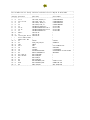
Table 1. Keywords for XRFS spectrum output and parameter files added to the standard format
for energy-dispersive spectra
Keyword
kVsetting
uAsetting
kVscaleIn
kVoffsetIn
uAscaleIn
uAoffsetIn
uAdividerR
kVscaleOut
kVoffsetOut
uAscaleOut
uAoffsetOut
RampInterval
kVdelta
uAdelta
kVstart
kVlimit
uAlimit
anode_z
kv
tube_inc_angle
tube_takeoff_angle
tube_be_window
filter_z
filter_thick
excit_angle
emerg_angle
solid_angle
path_type
inc_path_length
emerg_path_length
window_type
window_thick
minimum_energy
Description
X-ray tube kiloVolts Setting
X-ray tube microAmps Setting
kV Input Scale
kV Input Offset
uA Input Scale
uA Input Offset
uA Divider resistance (gigaOhm)
kV Output Scale
kV Output Offset
uA Output Scale
uA Output Offset
Ramp Interval (sec)
kV Ramp Delta
uA Ramp Delta
Minimum kV for Filament Start
kV Limit
uA Limit
X-ray tube anode atomic number
X-ray tube kiloVolts during acq.
X-ray tube electron incident angle
X-ray tube takeoff angle
X-ray tube Be window (mm)
Incident beam Filter atomic number
Incident beam Filter thickness (micron)
Incident beam Excitation angle (deg)
Fluorescence Emergence angle (deg)
Solid Angle (sterdian)
Atmosphere Path type
Incident path length (cm)
Emergence path length (cm)
Probe Window type
Probe Window thickness (micron)
Minimum analysis energy (eV)
35
Default value
20.00000000
5.00000000
-9.56999969
0.00000000
24.50000000
0.01000000
0.40500000
0.09380000
-0.14000000
0.04100000
0.10000000
1.00000000
1.00000000
5.00000000
10.00000000
40.00000000
25.00000000
47.00000000
20.21008301
90.00000000
51.11999893
0.50000000
1.00000000
0.00000000
38.86999893
74.12000275
0.00000850
2.00000000
0.94000000
1.97000003
2.00000000
0.00000000
1000.00000000
TR 0703
_______________________UNIVERSITY OF WASHINGTON • APPLIED PHYSICS LABORATORY_________________
Spectrum Processing (SP)
Description
This module calls another written in C++ to handle all of the computations. The
parameters needed by the physical model contained in the code are provided by the
spectrum processing module to the C++ module. The results of the spectrum analysis are
provided to the user in an on-screen list and to the spectrum display module. This
includes the calculated background and peak fits, the list of elements found in the
spectrum, and the weight fractions of each element with associated uncertainties (Figure
7). Net intensities of the associated peaks for each element are also displayed with the
intensity error from the Poisson statistics of the spectrum in the list on the lower right
corner of the interface.
The element identification and association of peaks with elements is fully automated but
is not entirely reliable. The quantitative results can be copied to the clipboard and made
available outside the program to prepare reports using the results of this instrument.
Functions
Background calculation and removal
Peak search
Element identification (associate peaks with elements)
Net peak intensity determination and calculated peak fits
Quantitative analysis (converting peak intensity to element weight percent)
Copy results to display
Spectrum Display (SD)
Functions
Plot spectrum vs. X-ray energy (Figure 5)
Overlay calculated background and peak fits
TR 0703
36
_______________________UNIVERSITY OF WASHINGTON • APPLIED PHYSICS LABORATORY_________________
Display markers at characteristic element emission line energies
Scale, zoom, and pan
37
TR 0703
_______________________UNIVERSITY OF WASHINGTON • APPLIED PHYSICS LABORATORY_________________
Instrument Performance Report
The purpose of this instrument is elemental analysis of regolith strata in a pre-drilled
borehole to investigate the subsurface of Mars and possibly other bodies within the solar
system. As such the primary performance criterion is the ability to quantify the elements
present in a particular stratum in an acceptable time and with sufficient accuracy to obtain
useful scientific information. For the purposes of this study, the detailed performance of
the sensor was evaluated by measurements on the actual prototype. The main
performance metric is the minimum detection limit (MDL). Improvements in the ability
to detect an element imply improvements in the ability to quantify the amount present.
Though there are some subtleties in this, the performance is dominated by the number of
X-rays present in the spectrum, which is dominated by the source strength given the
constraints on geometry and the available detectors for this instrument. The performance
was evaluated by measuring the detection limits of target elements in a light element
matrix.
The ability to accurately quantify a particular element is mainly limited by the precision
with which its X-ray emissions can be measured. This is determined by the statistical
variations in X-ray intensity due to the Poisson nature of their arrival times. In a given
time interval the number of X-rays that are detected has an intrinsic variance (the square
of the standard deviation) equal to the number of X-rays. This means that the relative
standard deviation is one over the square root of the number. For a given geometry and
sample composition, the number of X-rays detected from a particular element is
proportional to the source strength and the measurement time.
Detecting an element depends on both the number of X-rays collected from that element
and the background present even in the absence of that element. Because the background
is also subject to the same variations, the MDL is usually taken as three times the
TR 0703
38
_______________________UNIVERSITY OF WASHINGTON • APPLIED PHYSICS LABORATORY_________________
standard deviation of the background (converted to elemental concentration by an
appropriate calibration coefficient). This is equal to three times the square root of the
background counts in the spectrum. Both the desired signal and the background are
proportional to the source strength. The background arises from scatter of the continuum
from an X-ray tube and the detector peak-to-background ratio.
Materials and Methods
Standard Reference Materials
Standard Reference Materials (SRMs) numbered 2709, 2710, 2711, 97B and 2702 from
the National Institute of Standards and Technology were used for the characterization
tests. These SRMs are a set of selected soils with varying amounts of the basic soil
elements and extra elements in the form of contaminants. Concentrations ranged from
tens of percents for the basic soil components to below one part per million. This
provided a wide range to evaluate the instrument.
Samples were received from the National Institute of Standards and Technology as fine
powders. The samples were poured into specimen cups as received and presented to the
instrument without further preparation. Mars environmental conditions were simulated
on a laboratory bench-top using a glove bag. Eight millibar carbon dioxide partial pressure
was chosen as representative of the Mars atmosphere. A gas mix of three volume percent
carbon dioxide with helium making up the balance at Earth ambient pressure and gravity
provided the same carbon dioxide density typical of Mars atmosphere. All measurements
were made in this atmosphere.
39
TR 0703
_______________________UNIVERSITY OF WASHINGTON • APPLIED PHYSICS LABORATORY_________________
Determining the Minimum Detection Limit (MDL)
A spectrum is collected of a known sample containing the element for which the MDL is
desired. It is best to use a sample with a known element concentration less than 100
times the MDL. The largest peak from the element is found (usually K α or L α) and the
background is determined by a linear fit to the spectrum on either side of the peak. To
determine the total background counts the number of channels under the peak is
multiplied by the average counts in the channels on either side of the peak. The gross
peak counts are similarly determined by summing the counts in all channels under the
peak. The net counts from the element are the gross counts in the peak minus the total
background counts. Next the square root of the total background counts is multiplied by
three, then multiplied by the ratio of the known element concentration to the net counts
from the element. This yields the MDL in the same units as the known concentration.
Note that this procedure assumes a linear relationship between net counts and
concentration, which is a good assumption at low concentrations near the MDL. All
MDLs given in this instrument performance report were calculated using this procedure.
TR 0703
40
_______________________UNIVERSITY OF WASHINGTON • APPLIED PHYSICS LABORATORY_________________
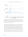
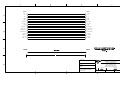
Figure 13. Raw spectra of five SRMs acquired with the borehole XRFS.
Test Plan Summary
•
Determine the MDL for the elements Mg, Zr, Cd, and Pb
•
Measure power consumption during spectrum collection
•
Dry, water saturated, and frozen sample
•
Variation with distance to probe (in case borehole diameter is not constant)
•
Measurement stability vs. time
•
Calibration linearity
41
TR 0703
_______________________UNIVERSITY OF WASHINGTON • APPLIED PHYSICS LABORATORY_________________
Results
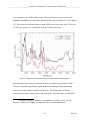
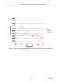
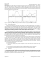
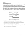
Figure 14 shows typical spectra from the borehole instrument. The specimen was a
terrestrial soil, SRM 2709, measured in the Mars simulated atmosphere. The silver target
X-ray tube was operated at 35 kV and 2 µA. No filters or other optics were used in the
incident beam. The detector has an internal collimator to restrict the beam to the center of
the diode. Data collection time was 1000 sec for the upper spectrum and 100 sec for the
lower spectrum. Note that the majority of the information is still available even with the
100-sec data collection time. This short data collection will greatly facilitate the
measurement of multiple strata in a borehole with vertical resolution of about 1 cm.
Figure 14. Spectra from borehole XRF spectrometer. Upper curve is 1000-sec data collection
time, and lower curve is 100 sec.
TR 0703
42
_______________________UNIVERSITY OF WASHINGTON • APPLIED PHYSICS LABORATORY_________________
As a comparison, the APXS (alpha proton X-ray spectrometer) spectra used on the
Pathfinder and MER rovers have little usable data above the iron peaks at 6.4 keV (Figure
15). The spectrum acquisition times for both APXS curves were many hours. The scale
is counts per second, so 1 corresponds to about 72,000 total counts.
3
Figure 15. Spectra from the APXS instrument. Reproduced with permission.
Detection limits for a number of elements in parts per million are presented in Table 2.
They are computed using the three sigma method and assuming a linear relationship
between net counts and the certified concentration. The background was linearly
interpolated from the counts on either side of the peak. Detection limits for each SRM
3
R. Reider, R. Gellert, J. Brückner, G. Klingelhölfer, G. Driebus, A. Yen, and S.W.
Squyres, J. Geophys. Res., 2003, 108, 8066–8078, DOI:10.1029/2003JE002150.
43
TR 0703
_______________________UNIVERSITY OF WASHINGTON • APPLIED PHYSICS LABORATORY_________________
are given, along with the average values. SRM 2710 has rather high concentrations of
many of the elements, so the linear concentration relationship may not hold. This causes
the detection limits to be larger in this material. They were included in the averages since
they have the effect of raising the detection limits, and including them avoids any bias
toward lower values.
None of the SRMs contained Mg at a level that gave an unambiguous peak. A compound
with magnesium as a major element was used to determine the magnesium detection limit.
Talc, or magnesium silicate hydroxide, is a readily available magnesium compound (as
baby powder, obtained from a local pharmacy) and was used for this purpose. Lowering
the X-ray tube voltage to 20 kV decreased the magnesium detection limit from about 3%
to the 1.4% value (Table 2). The ability to change the excitation conditions is another
strong argument for using an X-ray tube.
Measured power consumption is given in Table 3 for the system components and the
total. Ground support components including the safety interlocks and the USB computer
interface are not included, as these functions are either not necessary in a spacecraft or are
expected to be provided. The total power of 12 watts implies an energy requirement of
12 kJ per spectrum for a 1000-sec spectrum or 1200 J for a 100-sec spectrum. This is
comparable to the APXS energy per spectrum, with larger power consumption but
shorter collection times.
TR 0703
44
_______________________UNIVERSITY OF WASHINGTON • APPLIED PHYSICS LABORATORY_________________
Table 2. Minimum detection limits for several elements
Element
2702
2709
2710
2711
97B
Average
Mg
ND
ND
ND
ND
ND
1.4%
Ni
ND
8.9
2.0
ND
NP
5.5
Cu
8.2
4.2
16.2
8.9
NP
9.4
Zn
8.0
6.6
16.9
8.3
6.4
9.2
Pb
8.8
3.3
22.0
12.4
NP
11.6
NP
4.5
NP
4.1
4.8
4.5
Zr
ND = Not Detected
*
NP = None Present
Table 3. Power consumption during data collection
Function
Voltage
Current
Power
HV Power Supply
+14.84 V
0.426 A
6.31 W
X-ray tube control
+14.92 V
-14.92 V
+4.99V
0.150 A
0.149A
0.240A
4.46 W
Detector
Total
1.20 W
11.97 W
The effect on the measured spectrum from the presence of water is shown in Figure 16,
where spectra from dry, water saturated, and frozen specimens of SRM 2702 are
overlaid. There is almost no change in peak intensities, which is expected and indicates
that good quantitative information can be obtained regardless of water content. Also, the
presence of water will cause no significant degradation of detection limits. The region of
the spectrum that has peaks from coherent (Rayleigh) and incoherent (Compon) scatter
from the characteristic emission lines of the silver X-ray tube is shown in more detail in
Figure 17. Note that the scatter is much larger in the saturated and frozen specimens.
This increased scatter indicates presence of water and can be used to quantify the amount
of water present.
45
TR 0703
_______________________UNIVERSITY OF WASHINGTON • APPLIED PHYSICS LABORATORY_________________
Figure 16. Spectra of dry, water saturated, and frozen samples of SRM 2702. (Frozen spectrum
is 100 seconds to avoid thawing. It is multiplied by 10 for comparison.)
TR 0703
46
_______________________UNIVERSITY OF WASHINGTON • APPLIED PHYSICS LABORATORY_________________
Figure 17. Spectra of dry, water saturated, and frozen samples of SRM 2702. (Frozen spectrum
is 100 seconds to avoid thawing. It is multiplied by 10 for comparison.)
47
TR 0703
_______________________UNIVERSITY OF WASHINGTON • APPLIED PHYSICS LABORATORY_________________
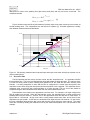
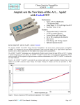
Figure 18. Variation in fractional change of total spectrum counts and iron intensity with distance
to probe. Tests conducted with SRM 2711. Note different scales.
TR 0703
48
_______________________UNIVERSITY OF WASHINGTON • APPLIED PHYSICS LABORATORY_________________
The results of varying the distance from the probe to the sample are given in Figure 18.
The intensity in the iron peak and the total counts in the spectrum are plotted as a
function of separation between the probe body and the sample surface. The plot on the
left shows the behavior in the first few millimeters and the plot on the right shows all of
the data taken for this test. Note that both of these measurements are stable to within 2%
for as much as 2 mm of separation. In addition, the normalized iron intensity, which is
the ratio of the iron peak to the total counts, is plotted as the green line. This quantity is
stable out to almost 5 mm, indicating that accurate quantitation can be performed even at
this distance. This is important since the diameter of the borehole may not be constant
and thus the distance between the probe and the regolith being measured may vary.
Because of the design, these expected variations will not affect the results of they are less
than 2 mm and can be compensated for out to 5 mm. Beyond 10 mm the spectrum is no
longer a reliable measurement of the sample.
49
TR 0703
_______________________UNIVERSITY OF WASHINGTON • APPLIED PHYSICS LABORATORY_________________
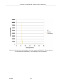
Figure 19. Variation in total spectrum counts over one week. (Point on Day 2 is after instrument
was in continuous operation for 4 hr.)
Results of the measurement stability test are given in Figure 19. Stability is about 2%
except for the final point. It is now known why this point is an outlier. The two points
on day 1 were taken when the instrument was first powered on and after several hours of
operation.
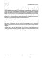
The calibration linearity was checked by plotting the composition measured by the
instrument against the certified composition for all elements in all of the SRMs (below 10
weight percent) (Figure 20). Except for two outliers and several false positives (the
points above the line near zero composition), the calibration is very good. The analysis
algorithm used here is a “standardless” algorithm that relies entirely on the fundamental
TR 0703
50
_______________________UNIVERSITY OF WASHINGTON • APPLIED PHYSICS LABORATORY_________________
parameters method to obtain the weight percent from the intensities in the spectrum. No
standards were used in calculating these results. This is an advanced method that is not as
good as careful use of type-specific standards, but was incorporated into the probe
software because standards that are similar to the planetary regolith may not be available,
especially if the subsurface regolith composition is unknown. Further work on the
fundamental parameters analysis algorithm should improve the calibration performance.
For the best results, appropriate standards with certified compositions can be used with
an empirical correction algorithm.
Figure 20. Measured vs. given composition for a wide range of elements in all five standard
reference materials.
51
TR 0703
_______________________UNIVERSITY OF WASHINGTON • APPLIED PHYSICS LABORATORY_________________
Conclusions
A borehole X-ray fluorescence spectrometer (XRFS) has been successfully constructed
and tested. Miniaturization has been performed to a diameter of 27.1 mm and
components can be configured in a variety of XRFS instrument designs. Modifications
can be easily incorporated, such as an SDD detector, the use of a different target X-ray
tube, or use of radioactive sources for excitation. Performance is very good, with
detection limits of about 10 ppm for many elements and detection of light elements down
to magnesium at 1.4%. Power consumption is 12 watts during data collection and the
total energy per spectrum is comparable to previous planetary inorganic analysis
instruments. Adequate data can be collected in 100 sec, facilitating investigation of strata
with vertical resolution of about 1 cm in a reasonable time.
TR 0703
52
_______________________UNIVERSITY OF WASHINGTON • APPLIED PHYSICS LABORATORY_________________
Appendices
All appendices are available on the CD-R that accompanies this report.
Appendix A. Digital Pulse Processor: User’s Guide and Operating
Instructions
Appendix B. X-ray Tube Product Documentation
Appendix C. Detector specification sheet
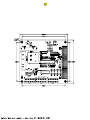
Appendix D. Borehole XRFS wiring diagrams
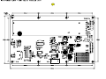
Appendix E. Borehole XRFS safety interlock/control board schematic
Appendix F.
Borehole XRFS HVPS power and control board schematic
Appendix G. Borehole XRFS head unit and umbilical cable schematics
Appendix H. Borehole XRFS safety interlock/control board layout
Appendix I.
Borehole XRFS HVPS power and control board layout
Appendix J.
Bill of materials for safety interlock control
Appendix K. Bill of materials for HVPS power and control board
Appendix L.
Borehole XRFS detector interface board schematic
Appendix M. Borehole XRFS detector interface board layout
Appendix N. Borehole XRFS safety controller software program by Peter
Sabin
53
TR 0703
Form Approved
OPM No. 0704-0188
REPORT DOCUMENTATION PAGE
Public reporting burden for this collection of information is estimated to average 1 hour per response, including the time for reviewing instructions, searching existing data sources, gathering and maintaining
the data needed, and reviewing the collection of information. Send comments regarding this burden estimate or any other aspect of this collection of information, including suggestions for reducing this
burden, to Washington Headquarters Services, Directorate for Information Operations and Reports, 1215 Jefferson Davis Highway, Suite 1204, Arlington, VA 22202-4302, and to the Office of Information
and Regulatory Affairs, Office of Management and Budget, Washington, DC 20503.
1. AGENCY USE ONLY (Leave blank)
2. REPORT DATE
3. REPORT TYPE AND DATES COVERED
December 2007
Technical Report
5. FUNDING NUMBERS
4. TITLE AND SUBTITLE
Borehole X-Ray Fluorescence Spectrometer (XRFS): User's Manual,
Software Description, and Performance Report
NNL05AA49C
6. AUTHOR(S)
W.C. Kelliher, I.A. Carlberg, W.T. Elam, and E. Willard-Schmoe
8. PERFORMING ORGANIZATION
REPORT NUMBER
7. PERFORMING ORGANIZATION NAME(S) AND ADDRESS(ES)
Applied Physics Laboratory
University of Washington
1013 NE 40th Street
Seattle, WA 98105-6698
APL-UW TR 0703
9. SPONSORING / MONITORING AGENCY NAME(S) AND ADDRESS(ES)
10. SPONSORING / MONITORING
AGENCY REPORT NUMBER
Cedric Mitchener
Office of Procurement, Research & Projects Contracting Branch
Mail Stop 126
9B Langley Blvd.
Hampton, VA 23681-2199
11. SUPPLEMENTARY NOTES
12a. DISTRIBUTION / AVAILABILITY STATEMENT
12b. DISTRIBUTION CODE
Approved for public release; distribution is unlimited
13. ABSTRACT (Maximum 200 words)
The X-ray fluorescence spectrometer (XRFS) is designed to be deployed down a pre-drilled hole for exploration and elemental
analysis of subsurface planetary regolith. The spectrometer excites atoms in the regolith and causes them to emit their characteristic X-rays. These characteristic X-rays produce peaks in the X-ray spectrum. By measuring the energy of the X-rays,
elements are identified. By measuring the intensity of the peaks, the amount of each element can be determined. A software
package operates the spectrometer, acquires the data, and analyzes the spectrum to provide elements and their weight fractions.
It also provides a user interface to control the measurements and display the results.
The spectrometer consists of two main subsystems packaged in three physical units. The main subsystems are the X-ray source
and the energy-dispersive X-ray detector. The source provides the X-rays to excite the specimen of regolith being investigated.
The energy-dispersive X-ray detector detects the emitted X-rays, determines their energy (the energy-dispersive function), and
counts the X-rays at each energy. Together these two subsystems measure the X-ray spectrum of the specimen.
14. SUBJECT TERMS
Mars, spectrometry, regolith, X-ray fluorescence, XRF, elemental analysis, inorganic analysis,
borehole
17. SECURITY CLASSIFICATION
OF REPORT
Unclassified
NSN 7540-01-280-5500
18. SECURITY CLASSIFICATION
OF THIS PAGE
Unclassified
19. SECURITY CLASSIFICATION
OF ABSTRACT
Unclassified
15. NUMBER OF PAGES
57 + CD-R
16. PRICE CODE
20. LIMITATION OF ABSTRACT
SAR
Standard Form 298 (Rev. 2-89)
Prescribed by ANSI Std. 239-18
299-01
DP4 User Manual D1.doc, 4/6/05
User’s Guide and Operating Instructions
Amptek, Inc.
6 De Angelo Dr.
Bedford MA 01730
781-275-2242
1
2
www.amptek.com
DP4 Design and Operation ..................................................................................................................3
1.1
Major Function Blocks...................................................................................................................3
1.2
DP4 Input ......................................................................................................................................4
1.3
Pulse Shaping and Selection ........................................................................................................5
1.4
DP4 Interface ..............................................................................................................................10
DP4 Specifications .............................................................................................................................11
2.1
Connections ................................................................................................................................11
Controls and Adjustments .....................................................................................................................15
3
Quick Start Instructions ......................................................................................................................18
3.1
Set-Up Instructions .....................................................................................................................19
3.2
Configuring the DP4....................................................................................................................21
3.3
Taking data .................................................................................................................................21
4
Control and Display Demonstration Software ....................................................................................23
5
Programmer’s Guide ..........................................................................................................................26
6
7
5.1
RS232 Serial Interface................................................................................................................26
5.2
USB Interface..............................................................................................................................26
Use of the DP4 with Amptek’s XR100 Detectors ...............................................................................35
6.1
Users with a Standard XR100 and PX2......................................................................................35
6.2
Users with a Standard XR100 without a PX2 .............................................................................38
6.3
Users with a DP4, PC4-3, and PA-210 Peamplifier....................................................................39
6.4
Analog Prefilter Circuit Description .............................................................................................41
6.5
Procedures for Common Changes .............................................................................................43
Dead Time in the Amptek DP4...........................................................................................................46
7.1
Fast Channel...............................................................................................................................46
7.2
Slow Channel ..............................................................................................................................47
Amptek Inc.
1
DP4 Digital Pulse Processor
7.3
DP4 User Manual D1.doc, 4/6/05
Acquisition Time..........................................................................................................................48
7.4
Timing Summary .........................................................................................................................49
8
Trouble-Shooting Guide .....................................................................................................................49
9
Index...................................................................................................................................................49
Amptek Inc.
2
DP4 Digital Pulse Processor
DP4 User Manual D1.doc, 4/6/05
1
DP4 DESIGN AND OPERATION
1.1
MAJOR FUNCTION BLOCKS
The DP4 is a component in the complete signal processing chain of a nuclear instrumentation system,
as shown in Figure 1. The input to the DP4 is the preamplifier output. The DP4 digitizes the preamplifier
output, applies real-time digital processing to the signal, detects the peak amplitude (digitally), and bins this
value in its histogramming memory, generating an energy spectrum. The spectrum is then transmitted over
the DP4’s serial interface to the user’s computer.
The Amptek DP4 has 6 main function blocks to implement these functions: (1) an analog prefilter, (2) an
ADC, (3) a digital pulse shaper, (4) pulse selection logic, (5) histogram logic, and (6) interfacing hardware
(which includes a microcontroller) and software. These six functions will be discussed below. Clearly, the
DP4 must be used with other components, including (at a minimum) a detector and preamplifier, a computer
with a serial interface and software to communicate, and a power supply.
DP4
Detector and
Preamplifier
Analog
Prefilter
ADC
Digital Pulse
Shaper
Pulse
Selection
Logic
Histogram
Logic
Microcontroller
&
Interface
Computer
Power Supply
Figure 1. Block diagram of the DP4 in a complete system.
It is important to recognize that the DP4 is designed for OEM use as part of a complete instrument. It
can also be tailored for laboratory use, but it is not intended as a stand-alone module for general purpose
use. Amptek’s PX4 is a general purpose laboratory module which includes the functionality of the DP4 and
much more, such as power supplies. Amptek strongly recommends the PX4 for non-OEM users.
The DP4 interface and control hardware are designed with considerable flexibility so the OEM user can
tailor it to a specific application. Amptek supplies software with the DP4 that includes two fully functional
demonstration programs. One program runs on the embedded microcontroller and interfaces between the
pulse shaping/histogram functions and a PC. The other program runs on a PC and interfaces between the
DP4 and the user. Both of these are intended as demonstration programs, which the user will tailor. The
DP4 also includes an FPGA. The FPGA logic, the “FPGA Configuration Bitstream”, is copyrighted by
Amptek, Inc. and may not be copied, modified, or used without the express, written approval of Amptek, Inc.
Analog Prefilter: The input to the DP4 is the output of a charge sensitive preamplifier. The analog prefilter
circuit prepares this signal for accurate digitization. The main functions of this circuit are (1) applying
appropriate gain, offset, and inversion (if necessary) to utilize the dynamic range of the ADC, and (2) carrying
out some filtering and pulse shaping functions to optimize the digitization.
ADC: The ADC digitizes the output of the analog prefilter at a 20 MHz rate. This stream of digitized values
is sent, in real time, into the digital pulse shaper.
Digital Pulse Shaper: The ADC output is processed continuously using a pipeline architecture to generate
a real time shaped pulse. This carries out pulse shaping as in any other shaping amplifier. The shaped
pulse is a purely digital entity. Its output can be routed to a DAC, for diagnostic purposes, but this is not
necessary. The peak value of the digital shaped pulse is determined by a peak detect circuit in the pulse
shaper. The peak value for each pulse, a single digital quantity, is the primary output of the pulse shaper.
Pulse Selection Logic: The pulse selection logic rejects pulses for which an accurate measurement cannot
be made. It includes pile-up rejection and risetime discrimination. These are discussed in more detail below.
Amptek Inc.
3
DP4 Digital Pulse Processor
DP4 User Manual D1.doc, 4/6/05
Histogram Memory: The histogram memory operates as in a traditional MCA. When a pulse occurs with a
particular peak value, a counter in a corresponding memory location is incremented. The result is a
histogram, an array containing, in each cell, the number of events with the corresponding peak value. This is
the energy spectrum and is the primary output of the DP4. The DP4 uses 3 bytes per channel, which allows
up to 16.7M counts per channel.
Interface: The DP4 includes hardware and software to interface between these various functions and the
user’s computer. A primary function of the interface is to transmit the spectrum to the user. The interface
also controls data acquisition, by starting and stopping the processing and by clearing the histogram
memory. It also controls certain aspects of the analog and digital shaping, for example setting the analog
gain or the pulse peaking time.
The interface includes a microcontroller and serial interface hardware. Both RS232 and USB interfaces are
currently implemented and described in this manual. The interface also contains an I2C interface and several
unallocated microcontroller pins that are available to the user. The interface includes two distinct software
packages, embedded software which runs on the microcontroller on the DP4 and acquisition and control
software that runs on the attached personal computer. The DP4 is shipped with a demonstration version of
the acquisition and control software package ( Visual Basic 5 source code is provided.) Source code for the
embedded software (8051 assembly language) is also available – contact Amptek for more information.
1.2
DP4 INPUT
The DP4 was designed to process signals coming directly from a charge sensitive preamplifier used
with a solid-state radiation detector. These signals typically have (1) a small amplitude, in the range of a few
mV, (2) a fast rise (tens of nsec to µsec), and (3) following the signal, either a slow decay (of order msec) or
no decay. A charge sensitive preamplifier integrates the current into its input, so over time the output drifts
towards the rail. One of two methods is usually used to restore the output.
Some preamplifiers use a pulsed reset to periodically restore the input charge. In such preamps, there
is no tail after the signal. A radiation interaction generates a voltage step, then the output is constant until
the next step, as illustrated in Figure 2(a). Eventually, the output will drift near the supply rail and is then
reset to its initial value, leading to a very large and fast reset signal. The DP4 is configured from the factory
for use with such reset-type preamplifiers. The reset results in a large, negative going pulse into the ADC,
which disrupts the signal processing. The preamplifier output can take a significant time to fully recover from
a reset. Pulses received during reset recovery will have a distorted amplitude and degrade the spectrum.
Therefore the DP4 includes hardware to lock out data acquisition during reset.
(a)
(b)
Figure 2. Oscilloscope traces showing typical preamplifier outputs, for reset (a) and continuous (b)
preamplifiers. The DP4 is shipped from the factory configured for the reset inputs, such as those on the left.
Amptek Inc.
4
DP4 Digital Pulse Processor
DP4 User Manual D1.doc, 4/6/05
Some preamplifiers use a continuous feedback, the simplest of which is a resistor in parallel with the
feedback capacitor. After the voltage step due to each signal interaction, the output slowly drifts back to its
quiescent value, with the time constant of the feedback, as illustrated in Figure 2(b). This time constant is
long, 500 µsec in this case, so that the charge in the signal can be accurately integrated. The DP4 hardware
may be configured for use with most continuous feedback preamplifiers. This is discussed in Section 0
1.3
1.3.1
PULSE SHAPING AND SELECTION
Pulse Shaping
The DP4 implements trapezoidal pulse shaping, with a typical output pulse shape shown in Figure 3.
This shape was chosen because it provides a near optimum signal to noise ratio for many detectors,
including Amptek’s XR100 detectors under normal operating conditions. The user can adjust the rise/fall
time (the rise and fall must be equal) and the duration of the flat top. These values can be set to a large
number of discrete values, shown in Table 1.
A semi-gaussian amplifier with shaping time τ has a peaking time of 2.2τ and is comparable in
performance with the trapezoidal shape of the same peaking time. So, if the DP4’s digital shaper were to be
set to the equivalent of an analog amplifier with a 12 µs shaping time constant it would be set to roughly
2.2*12 = 26.4 µs peaking time.
The electronic noise of a detector will generally have a minimum at some peaking time, the “noise
corner.” At peaking times shorter or longer than this, there is more noise and hence degraded resolution. If
this peaking time is long relative to the rate of incoming counts, then pulse pile-up will occur. In general, a
detector should be operated at a peaking time at the noise corner, or below the noise corner as necessary to
accommodate higher count rates.
If the risetime from the preamp is long compared with this peaking time, then the output pulses will be
distorted by ballistic deficit. In this case, the trapezoidal flat top can be extended to improve the spectrum.
The specific optimum timing characteristics will vary from one type of detector to the next and on the details
of a particular application, e.g. the incoming count rate. The user is encouraged to test the variation of
performance on these characteristics.
Figure 3. Pulse shape produced by the DP4.
Amptek Inc.
5
DP4 Digital Pulse Processor
DP4 User Manual D1.doc, 4/6/05
Peaking
Time (uS)
0.8
1.6
2.4
3.2
4.0
4.8
5.6
6.4
8.0
9.6
11.2
12.8
16.0
19.2
22.4
25.6
32.0
38.4
44.8
51.2
64.0
76.8
89.6
102.4
Flat Top
(uS)
0.2...3.2
0.2...3.2
0.2...3.2
0.2...3.2
0.2...3.2
0.2...3.2
0.2...3.2
0.2...3.2
0.4...6.4
0.4...6.4
0.4...6.4
0.4...6.4
0.8...12.8
0.8...12.8
0.8...12.8
0.8...12.8
1.6...25.6
1.6...25.6
1.6...25.6
1.6...25.6
3.2...51.2
3.2...51.2
3.2...51.2
3.2...51.2
Decimation
1
1
1
1
1
1
1
1
2
2
2
2
4
4
4
4
8
8
8
8
16
16
16
16
'Rise'
register
1
2
3
4
5
6
7
8
5
6
7
8
5
6
7
8
5
6
7
8
5
6
7
8
Flat Top
register
0…15
0…15
0…15
0…15
0…15
0…15
0…15
0…15
0…15
0…15
0…15
0…15
0…15
0…15
0…15
0…15
0…15
0…15
0…15
0…15
0…15
0…15
0…15
0…15
Decimation
register
0
0
0
0
0
0
0
0
1
1
1
1
2
2
2
2
3
3
3
3
4
4
4
4
Table 1. Table of allowed rise/fall times (peaking times) and flat top times.
The pulse shaping of the DP4 is illustrated in Figure 4. The top trace shows the input to the DP4, which
is the output from a reset-type charge sensitive preamplifier. This is processed by the analog prefilter (see
Figure 1), producing the prefilter output shown at the bottom. This is digitized and then processed digitally,
producing the DP4’s shaped output, also shown at the bottom.
1) DP4 Input (Preamp Output)
5 mV/div 20 µsec/div
2) Prefilter Output
(ADC Input)
3) DP4 Shaped
Output
Both traces: 200 mV/div 20 µsec/div
Figure 4. Oscilloscope trace illustrating the normal operation of a DP4.
Amptek Inc.
6
DP4 Digital Pulse Processor
DP4 User Manual D1.doc, 4/6/05
1.3.2
Baseline Restoration (BLR)
The “baseline” of a digital processor has some significant differences from traditional analog shaping
amplifiers. Traditional amplifiers generally include some form of baseline restoration, DC feedback, to
prevent drift at high count rates. Because the DP4’s transfer function has a finite impulse response, after a
pulse has passed through the processing pipeline it has no impact on the output. This is fundamentally
different from an analog differentiator and results in vastly enhanced baseline stability at high count rates.
However, unlike analog shapers the DP4 has to establish a DC baseline, at all count rates. There are two
options available in the DP4 to establish the DC baseline: “auto-baseline”, which involves measuring the
input offset, and baseline restoration, which uses closed loop, quasi-DC feedback.
1.3.2.1
Auto-Baseline
The ‘Auto-Baseline’ function does not correct baseline variations resulting from count-rate changes or
other detector effects; rather, it corrects for drift in the DP4’s analog section, due mostly to temperature
changes. It is intended to be used with reset-style preamps that do not otherwise require BLR (i.e. the
Amptek XR100CR). When the DP4 detects that reset has occurred, it temporarily disconnects the detector
from the DP4 front-end electronics and averages the voltage offset produced by the front end. The detector
is reconnected and the measured offset is used to correct the digital baseline. This doesn’t affect throughput
since the processing is suspended anyway during reset to allow the preamp signal to settle.
1.3.2.2
BLR
The DP4 also has an asymmetric baseline restorer, which can be used when baseline shifts due to
count-rate changes, power supply drift, or if other detector effects need to be nulled. It works as follows:
a.
All digital samples below the existing baseline are integrated. When the sum reaches a preset
value (the “BLR Correction Threshold”), an upward correction (the “Baseline Up Correction”) is
added to the baseline.
b.
Countering this occasional upward correction is a periodic downward correction (the “Baseline
Down Correction.)
As the magnitude of these corrections is typically much less than one channel, the periodic downward
correction and occasional upward correction should not adversely affect resolution. Each of the corrections
has four settings (very slow, slow, medium and fast) and the correction threshold also has four settings (very
fast, fast, normal and slow.) It should be noted that the relative size of these corrections is dependent on
peaking time; thus a setting that works well at a particular peaking time may not necessarily be ideal for a
different peaking time.
BLR and Auto-Baseline should not be used at the same time.
1.3.3
1.3.3.1
Pulse Selection
Pile-Up Rejection
The goal of the pile-up reject (PUR) logic is to determine if two interactions occurred so close together in
time that they appear as a single output pulse with a distorted amplitude. The DP4 PUR uses a “fast-slow”
system, in which the pulses are processed by a fast shaping channel in parallel with the slower main channel
(both channels are purely digital). Though similar in principle to the techniques of an analog shaper, the pileup reject circuitry and the dead time of the DP4 differ in significant ways, resulting in much better
performance at high count rates. First, the symmetry of the shaped pulse permits the dead time and pile-up
interval to be much shorter. Second, there is no dead time associated with peak acquisition and digitization,
only that due to the pulse shaping. [Setting 0 = off].
Figure 5 illustrates the operation of the DP4 for pulses that occur close in time. Figure 5 (a) shows two
events that are separated by less than the rise time of the shaped signal, while Figure 5 (b) shows two
pulses that are separated by slightly longer than the rise time. In (a), the output is the sum of the two signals
(note that the signal amplitude is larger than the individual events in (b)) and the events are said to be piled
up. However, note that the analog prefilter outputs in (a) are separate. For a nearly triangular shape, pile-up
only occurs if the two events are separated by less than the peaking time, in which case a single peak is
observed for the two events. The interval used by the DP4 for both dead time and pile-up rejection is the
Amptek Inc.
7
DP4 Digital Pulse Processor
DP4 User Manual D1.doc, 4/6/05
sum of risetime, plus about 20% of the risetime to account for jitter, and the flat-top duration. If two events
occur within this interval and pile-up rejection is disabled, then only the single, piled-up value is in the
spectrum. If pile-up rejection is enabled and two events are separated by more than the fast channel pulse
pair resolution (600 nsec) and less than this interval, both are rejected. Events that exceed a threshold in the
fast channel trigger the pile-up reject logic.
(a)
(b)
Figure 5. Oscilloscope traces illustrating the dead time and pile-up reject performance of the DP4
1.3.3.2
Risetime Discrimination
In some types of detectors, pulses with a slow risetime have a charge amplitude deficit. For example, in
many diodes there is an undepleted region with a weak electric field. A radiation interaction in this region will
generate a signal current, but the charge motion is slow through the undepleted region. This leads to a slow
rising edge on the pulse and since charges are trapped, a small pulse. Interactions in this region can lead to
various spectral distortions: background counts, shadow peaks, asymmetric peaks, etc. In risetime
discrimination, events with a slow rise do not contribute to the spectrum but are rejected.
The DP4 implements RTD by measuring the width of the fast channel response: a slower input rise time
leads to a broader fast channel output. Because a broader fast channel output also has a lower amplitude (to
maintain the same net area), the DP4 measures the Half-Width, Half-Max (HWHM) of the resulting response.
This measured width is compared to a preset width (the “RTD Time Threshold”) and the event is rejected if
the measured width is too wide. [Note that the event can only be rejected if the Fast Channel is over
threshold. See the next section for a discussion of thresholds.]
Because the fast channel is inherently much noisier than the slower shaped channel, an RTD threshold
is also implemented on the shaped channel. Events which fall below this threshold (the “RTD Slow
Threshold”) are not processed by the RTD and are thus accepted (unless otherwise rejected by Pileup
Rejection or some other criterion). Because RTD is most often needed on interactions deep in a detector,
arising from high-energy events, low-amplitude events are unlikely to benefit from RTD rejection. These fall
below the RTD Slow Threshold and are thus accepted.
To summarize the RTD rules:
a. Events whose shaped (slow) channel amplitude is below the RTD Slow Threshold are kept;
otherwise…
b. Events whose fast channel amplitude is below the fast threshold are rejected; otherwise…
c.
1.3.3.3
Events whose measured HWHM is wider than the RTD Time Threshold are rejected.
Thresholds
Slow channel threshold: The DP4 uses the Slow Channel Threshold to distinguish between events that
should be added to the stored spectrum and those that shouldn’t. Events with an amplitude lower than the
Slow Channel Threshold are ignored – they do not contribute to the stored spectrum. The slow channel
threshold is the equivalent of a low-level discriminator (LLD).
Amptek Inc.
8
DP4 Digital Pulse Processor
DP4 User Manual D1.doc, 4/6/05
Fast Channel Threshold: The Fast Channel Threshold is used for two functions: Rise Time
Discrimination (RTD), as described in section 1.3.3.2, and Pile-up Rejection (PUR). The DP4 can only reject
piled-up events if both events fired the fast channel; therefore, it is usually desirable to set the Fast Channel
Threshold as close to the noise as is practical. This is discussed in more detail in later sections. If RTD and
PUR are not used, then the fast channel threshold is not important.
1.3.3.4
Gate
The gate input is used with external circuitry to determine if events should be included or excluded from
the spectrum. The gate can be active high or active low (or disabled). If disabled, then this input is ignored
and all events (which meet the criteria above) are counted. If active high (low), then if the gate input is high
(low), the event is counted in the spectrum. When counts are gated off, the clock is also gated off so that an
accurate count rate can be determined.
The timing of this gate input is important. If the gate input is active while the fast channel threshold is
triggered, then the event is counted as a fast count. If the gate input is active when the peak detect is
triggered, then the event is counted as a slow count and shows up in the spectrum. Note that the fast and
slow channels are triggered at different times, since they have different shaping times. We recommend that
the gate input duration be equal to or greater than the sum of the peaking and flat top durations.
1.3.4
Multichannel Analyzer
The MCA portion of the DP4 supports 256, 512, 1024, 2048, 4096 or 8192 channels. (8192 channels is
only available via the USB interface – it is not supported via RS232.) The DP4 uses 3 bytes per channel,
which allows up to 16.7M counts per channel. The MCA has two spectral buffers available, A and B, which
can be selected either via software, or by a hardware signal.
1.3.5
Single Channel Analyzer
The DP4 contains eight single channel analyzers (SCAs). Each SCA has an upper and a lower
threshold. If an event occurs with a shaped output within the range defined by these thresholds, then a logic
pulse is generated and is output to the JP9 connector on the DP4, where it can be connected to external
hardware. The upper and lower limits of the 8 SCAs can be set independently in the software. SCA8 serves
a dual purpose – not only does it operate like the other SCAs, but it is also used to set the Region-of-Interest
(ROI) for the Preset Count mode of MCA operation. That is, when a Preset Count is selected, the MCA will
stop after the programmed number of counts occurs in the SCA8 ROI.
Amptek Inc.
9
DP4 Digital Pulse Processor
DP4 User Manual D1.doc, 4/6/05
1.4
DP4 INTERFACE
There are two distinct components to the DP4 software. The microcontroller on the DP4 contains
embedded software that controls data acquisition and the interface. The computer to which the DP4
interfaces must contain software to communicate via the serial port (USB or RS-232). The current revision of
the DP4 is designed primarily for use in OEM applications, embedded in an end-user’s product. As such, the
user may access the embedded software to tune the instrument for his/her application. Further, the personal
computer software that is supplied is essentially a demonstration program. It permits the user to fully access
the DP4 functionality and can be used as is, but more importantly it shows how to carry out the various
functions. We presume that the user will tailor this software to meet the specific requirements of his/her
application.
The DP4 has both a USB interface and a standard RS232 interface. Specifically, it has a full-speed
(12Mbps) USB 1.1 interface (which is also compatible with newer USB 2.0 ports.) Amptek has licensed a
USB device driver for use with Windows 98, Windows ME, Windows NT, Windows 2000 and Windows XP,
which makes it easy to write Windows software to communicate with the DP4.
Note on the USB device driver
The USB device driver is licensed from Andrew Pargeter & Associates (www.devicedriver.com) for the
Amptek DP4. The license agreement allows Amptek to provide the driver to the OEM, and the OEM to
provide the driver to the end user provided that the embedded code doesn’t change. In practice, an OEM
who wishes to write his own embedded code will either need to relicense the USB driver or find another
driver solution. If the OEM wishes only minor changes to the existing embedded code, he should contact
Amptek to see if the changes could be made to the standard code, and thus would be covered by the license
agreement.
The USB Vendor ID (VID) and Product ID (PID) are provided to Amptek from Andrew Pargeter &
Associates (“APA”) as part of the license agreement. The VID (0x0BD7) is owned by APA, and the PID
(0xA021) is licensed for use only with the Amptek DP4. OEMs may not use this VID/PID combination, except
with the standard Amptek DP4 embedded code. Contact Amptek for more information. For more information
on VIDs & PIDs, refer to the USB Implementer’s Forum (www.usb.org).
Amptek Inc.
10
DP4 Digital Pulse Processor
DP4 User Manual D1.doc, 4/6/05
2
DP4 SPECIFICATIONS
2.1
DIMENSIONS
2.2
CONNECTIONS
There are two primary connectors, which are necessary for the DP4’s operation, along with some
auxiliary connectors. JP7 is the analog input, which connects to a preamplifier output. JP6 contains the
power supply connections and the serial interface. These are the primary connectors and are required for
operation. Their use is shown graphically in Figure 6.
Amptek Inc.
11
DP4 Digital Pulse Processor
DP4 User Manual D1.doc, 4/6/05
DP4
2
3
GATE
BUFFER_SEL
GND
1-8
9
10
11,12
JP9
JP7
1
SCA1-8
J2
AMP3
IN+
IN-
Digital
Processor
ADC
FILTER
DAC
GND
MCA
Memory
+3.3V
JP6
1
+5V
2
-5V
GND
3
4,5
OUT
2
GND
µprocessor
6,7
8,13
9-12
14
15,16
2
GND
RS232
/RST
USB
IC
1
or
+3.3V
+5V
-5V
GND
POWER
Figure 6. Block diagram illustrating the primary connections.
The auxiliary connectors include (1) an analog output, the output of a DAC, J2; (2) a proprietary test
connector, JP5; (3) an external I/O connector with SCAs, GATE and BUFFER_SEL, JP9; and (4) a user
connector, JP10, which is tied to four microcontroller pins.
2.2.1
JP7 – Analog input
This is the input to the DP4 from a preamplifier. +IN and –IN form a differential input to the DP4, which
is an inverting amplifier.
•
Pin 1: +IN: Non-inverting input. For negative pulses, connect signal to +IN and return to –IN.
•
Pin 2: -IN: Inverting input. For positive-going pulses, connect signal to –IN and return to +IN.
•
Pin 3: AGND: Analog ground.
Connector:
•
The JP7 connector on the DP4 is a Molex P/N 22-05-3031. Mating connector is: Molex P/N 22-01-3037
(Digi-Key P/N WM2001-ND) with Molex crimp terminals P/N 08-50-0114 (Digi-Key P/N WM1114-ND).
Requirements:
•
Polarity: The DP4 is an inverting amplifier. Measured at Pin 1 referenced to Pin 2, the input pulse
should be negative. The connector should be wired to achieve this as discussed above.
•
Magnitude: The inputs to the first amplifier stage have a common mode range of +7.6V, with a
differential mode range of +3.8V. By default, a 25% attenuator is installed (R291=R296=330 ohms) to
increase the common mode range to +9.5V and the differential mode range to +4.75V. If this increased
range isn’t needed, the attenuator can be removed (R291=R296=0 ohms). See section 2.3.1.
Amptek Inc.
12
DP4 Digital Pulse Processor
•
DP4 User Manual D1.doc, 4/6/05
The default configuration is for reset preamps. For continuous feedback preamplifiers, the hardware will
require reconfiguration, as discussed in Section 0.
•
Risetime >100 nsec
2.2.2
JP6 – Power and Interface
JP6 is a 16-pin 1mm flex connector.
Pin #
Name
Pin #
Name
1
+3.3V
9
RS232-RX
2
+5V
10
RS232-TX
3
-5V
11
RS232-CTS
4
GND
12
RS232-RTS
5
GND
13
GND
6
I2C SDA
14
/RESET
2
7
I C SCL
15
USB-
8
GND
16
USB+
Table 2. Pinout for JP6, the primary power and serial interface connector
•
+3.3V: This supply powers the majority of the DP4. Average operating current is 100-200mA,
depending on configuration. Peak current is 500 mA at startup.
•
+5V, -5V: These supplies power the analog front end. Average operating current is 10 mA for each.
These should be well filtered, since ripple is likely to degrade performance. There is no overcurrent or
reverse voltage protection implemented on the DP4.
•
SDA, SCL: These are the I2C bus signals. The DP4 microcontroller is the bus master, so any
peripherals connected to the I2C bus must be slaves. The only I2C devices on the DP4 (other than the
µC) are the 24AA64 boot prom and a temperature sensor.
•
RS232-RX, RS232-TX, RS232-CTS, RS232-RTS: These are RS232 signals for interfacing the DP4 to
a host system. The signal names are relative to the DP4, i.e. the DP4 receives on the RX pin and
transmits on the TX pin. The handshaking signals CTS and RTS are not used but are available for
custom applications.
•
/RESET: Pulling this signal low will hold the entire DP4 in reset. Floating it or pulling it high allows
normal operation.
•
USB+, USB-: This is the USB (Universal Serial Bus) communication bus. The DP4 microcontroller
contains a USB communication core.
Connector:
•
Connector: 16 position right angle, Hirose Electronic Co. Ltd: FH21-16S-1DS, Digi-Key: HFG16T-ND
•
Mating cable: 1mm Flat Flex Cable 4", Parlex: 100-16-102B, Digi-Key: HF16U-04-ND (other lengths are
available)
2.2.3
J2 – Analog output
This is the shaped output from the DAC. The decimated input and other diagnostic signals can also be
output from the DAC.
•
Pin 1: +OUT: This is the output of the DAC. Output range is 0-1V.
Amptek Inc.
13
DP4 Digital Pulse Processor
•
DP4 User Manual D1.doc, 4/6/05
Pin 2: AGND: Analog ground. Care should be taken in connecting this ground externally, as ground
currents can disturb the analog front end.
Connector:
•
The J2 connector on the DP4 is a Molex P/N 22-05-3021. Mating connector is: Molex P/N 22-01-3027.
(Digi-Key P/N WM2000-ND) with Molex crimp terminals P/N 08-50-0114 (Digi-Key P/N WM1114-ND)
2.2.4
JP9 External Logic I/O
JP9 is an 8x2 2mm header, which offers functionality which is required by some but not all users. Pins
1 through 8 are the outputs of the single channel analyzer outputs, discussed in section 1.3.5. Pins 9 and 10
are the gate input (section 1.3.3.4) and buffer select input (section 2.3.4), respectively. Pins 11 and 12 are
ground.
Pin
Function
Pin
Function
Pin
Function
1
SCA1
5
SCA3
9
GATE IN
2
SCA8
6
SCA6
10
BUFFER SEL
3
SCA2
7
SCA4
11
GND
4
SCA7
8
SCA5
12
GND
GATE and BUFFER_SEL inputs:
VIL (logic low): -0.5 to + 0.7V
VIH (logic high): +2.4 to +5.5V
Inputs: SN74LVC2G14, Vcc=3.3V, 100 kΩ pull-downs
SCA Outputs:
VOL (logic low): 0.1V @ 100uA
VOH (logic high): +3.1V @ 100uA
Outputs: SN74LVC245A, Vcc=3.3V, 49.9 Ω series termination
Pulse width: 50nS
2.2.5
J15 I2C Bus
J15 includes the I2C bus signals (SCL & SDA), and a global active low reset input (/RESET). This
header can be used for in-circuit programming of the microcontroller EEPROM, or it can be used by custom
applications to communicate with other I2C devices.
2.2.6
Diagnostic Testpoint .5
The DP4 has a diagnostic testpoint, labeled ‘.5’, which is located near the FPGA (see picture below).
This testpoint can be configured via the application software to output a number of useful signals, as listed
below:
Amptek Inc.
Signal Name
Function
ICR
Input Count Rate, i.e. Fast Channel fired
PILEUP
Piled-up event detected
HOLD
(Internal diagnostic)
ONESHOT
Period during which a 2nd event would be considered piled-up
DET_RES_
Active-Low Detector Reset Lockout Period
14
DP4 Digital Pulse Processor
DP4 User Manual D1.doc, 4/6/05
2.2.7
MCA_EN
High=MCA Enabled, Low=MCA Disabled
TRIGGER
Peak Detect Fired
SCA8
Single Channel Analyzer output #8 (Also available on JP9)
JP10 Extra signals for OEM use
JP10 contains signals from four unused pins on the microcontroller. These pins are configured as
outputs, and can be controlled via USB commands (See section 5.2.1). The outputs go between 0V (0.4V @
-1.6mA) and +3.3V (+2.4V @ 1.6mA).
Pin #
Function
1
Output #1
2
Output #2
3
Output #3
4
Output #4
5
GND
CONTROLS AND ADJUSTMENTS
2.3
2.3.1
Analog Prefilter
•
Inversion: On JP7, pins +IN and –IN form a differential input. The DP4 requires a negative pulse on
+IN relative to –IN.
•
Input Attenuation: If the signal exceeds the nominal range of +/- 3.8V, R291 & R296 can be used to
attenuate the input signal. R291=R296=330 ohms yields 25% attenuation (the default configuration);
1Kohm yields 50% attenuation.
Amptek Inc.
15
DP4 Digital Pulse Processor
•
DP4 User Manual D1.doc, 4/6/05
Coarse Gain: Four coarse gain settings are available, by command from the microcontroller. The gain
settings are x10.8, x20.7, x55.4, and x106.2.
•
Fine Gain: Fine gain is adjusted digitally, via software, over a range of +/- 25%.
•
Offset: The pot R287 sets the DC offset into the ADC. The ADC input should never drop below zero, or
significant distortions in the pulse shape will occur.
•
Input Pole: The pot R297 is used to set an input pole, part of the prefilter function.
2.3.2
Pulse Shaping
•
Rise and Fall Time: The rise time of the shaped pulse, which must equal the fall time, can be set to any
one of several values, listed in Table 1. This is adjusted digitally: the microcontroller writes the desired
value to a register in the pulse shaping hardware. The demonstration software provides a simple
control for this. Setting this value by the demonstration software is described in sections 3.2.2 and 4.
•
Flat Top Duration: The duration of the trapezoidal flat top can also be set to one of several values, by a
digital command.
•
Decimation: For long rise times, the input ADC values are decimated, as is common with digital
processing. The decimation setting is related to the rise/fall time and the flat top duration. This is also
set by digital command.
•
DAC Controls: The DAC has several controls, described more fully in section 5. The DAC provides an
analog display of the digital processing that is occurring. The analog display is not needed but is
convenient for setup and debugging. First, the DAC can be enabled or disabled. Second, several
different waveforms may be sent to the DAC. This includes the fast channel output, the decimated
input, the shaped output, and the BLR correction. Third, a DC offset can be sent to the DAC. The DAC
responds to underflows (outputs below 0V) by wrapping over, so it is recommended practice to set a DC
offset that avoids this.
•
Preamp Reset Controls: These are utilized with reset type preamps and their operation is described in
section 1.3.2.1. The user may enable or disable Autobaseline. The user may also set a reset period,
which is the length of time following a reset signal during which data processing is shut down, to permit
the electronics to fully recover. The user may also elect to disable reset detection. These controls are
sent by software to the pulse processing FPGA.
•
Baseline Restoration Controls: The operation of the baseline restorer is described in section 1.3.2.2.
The user may enable or disable BLR. If enabled, then the user may choose to set three parameters:
up, down, and threshold, each set to one of four values. “Up” (“Down”) determines the size of the
upward (downward) step to the baseline. “Threshold” determines when an upward correction is
required. These controls are sent by software to the pulse processing FPGA. Autobaseline should be
disabled if BLR is enabled or if a non-reset style preamp is used.
Amptek Inc.
16
DP4 Digital Pulse Processor
DP4 User Manual D1.doc, 4/6/05
2.3.3
Pulse Selection
•
Fast Threshold: A low level threshold for the fast channel can be set by a digital command. The logic
output is used in subsequent pulse processing.
•
Pile-Up Rejection: The pile-up rejection (PUR) has one direct control, the on/off control. Indirectly, the
operation of the PUR is greatly affected by the setting of the Fast Channel Threshold. Only signals with
a fast channel response exceeding this threshold are evaluated for possible pile-up. If this threshold is
set too low, then electronic noise triggers the PUR detect circuits. Pulses are rejected if they occur
close in time with noise, and therefore there is very low data throughput. If this threshold is set too high,
then real events are missed and therefore pile-up will be present in the spectrum. Common practice is
to set the fast threshold to generate 5-10 cps, in the absence of any signal, which puts this level as
close to the noise as possible without degrading throughput.
•
Pile-up period: the pile-up period (the minimum interval between two successive peaks which are not
considered piled up) is programmable. The optimal setting is:
(RisetimeRegister * 19 + (FlatTopRegister + 1) * 4) / 2.
•
Risetime Discrimination: Risetime discrimination is described in section 1.3.3.2. There are three
controls, each sent via software to the FPGA. First, RTD may be enabled or disabled. Second, if
enabled, then the user may set the threshold. This threshold applies to the slow channel. Only events
exceeding this threshold will be analyzed by the RTD circuit; all events below this threshold are
accepted. Third, the user may set the HWHM for the fast channel. Only events with a HWHM below
this value will be accepted.
2.3.4
MCA Control
•
Number of channels: The MCA can be set to have 256, 512, 1024, 2048, 4096, or 8192 channels.
•
Slow Channel Threshold (LLD): As with most MCAs, there is a low level discriminator on the slow
channel. Only pulses exceeding this threshold will be recorded in the MCA spectrum. The register
setting of 0-255 corresponds to about 0-25% of the full-scale output.
•
Gate: In software, the user may set the gate “off”, in which case the gate input is ignored. The user
may also set it to active high or active low.
•
Buffer: There are two memory buffers in the hardware, designated A and B. The user may choose to
use either. In addition, the user may choose to enable “Hardware Select”. If this is enabled, then an
external logic input controls whether the data go into buffer A or B.
•
Preset Time: The accumulation time may be preset, from 100ms to 19.4 days, with 100ms precision.
This is set in software. After this time has elapsed, acquisition will stop. This will be the accumulation
time, the duration of data acquisition, not live time and not elapsed clock time. See section 7.3 for
details on accumulation time.
•
Preset Counts: The DP4 can be programmed to acquire a preset number of counts in a region of
interest. Acquisition will stop when this number of counts is reached. SCA8 must be configured with the
region of interest.
2.3.5
SCA Controls
There are 8 SCA channels, each of which has the following three controls.
•
Enable: If this is selected, then that channel outputs counts.
•
Lower and Upper Thresholds: These define the range of the SCA. These are in MCA channels: if the
MCA is is 1024 channel mode, and SCA 1 has a range of 712 to 800 for example, then any time a count
is binned in this range of MCA channels, there will be a logic pulse on the SCA output.
Amptek Inc.
17
DP4 Digital Pulse Processor
DP4 User Manual D1.doc, 4/6/05
3
QUICK START INSTRUCTIONS
The purpose of this section is to provide enough information to set up the DP4 hardware, install the
demonstration software, and start taking data. More detailed information on the hardware and software is
elsewhere. In particular, the interface software which runs on the personal computer is described in more
detail in section 4. The most important connectors and controls are shown below.
JP9 SCA outputs, Gate
& Buffer_Sel inputs
JP7 Analog Input
Connector
AMP3
Test Point
J2 Analog Output
Connector
R287 Offset
Adjust
JP6 Power &
Interface Connector
.
Amptek Inc.
18
DP4 Digital Pulse Processor
DP4 User Manual D1.doc, 4/6/05
3.1
3.1.1
SET-UP INSTRUCTIONS
Software installation and serial port connection (USB)
1) All of the necessary software is on the CDROM. Run the ‘setup’ program in the DP4 folder to install the
compiled Visual Basic software. [The Visual Basic source code is in the ‘Source Code\VB’ folder]
2) Connect the USB interface, per section 2.2.2 on page 13, to the USB port of a personal computer or hub.
[A USB ‘A’ to ‘B’ cable is required to connect between the USB connector on the optional DP4 connector
or power supply boards (PC4-1,2,3) and the USB port of a PC or hub.] Apply power to the DP4; the ‘New
Hardware Wizard’ should automatically start on the PC. Follow the directions below to install the USB
device driver, depending on which version of Windows is in use.
3) For Windows 2000 or Windows XP:
a. In the “Found New Hardware Wizard” (which should automatically appear when the DP4 is
connected and powered on for the first time), select “Install from a list or specific location”,
and click “Next >”.
b. Select “Don’t Search. I will choose the driver to install.” and click “Next >”.
c.
Click the “Have Disk…” button.
d. Select “Browse…” and navigate to the \USB_driver\Win2K_XP folder of the DP4 CDROM.
Select “OK”.
e. Click “Next >”.
f.
Click “Finish”. The USB driver should now be installed.
4) For Windows 98 or Windows ME:
a. The “Add New Hardware Wizard” should automatically appear when the DP4 is connected
and powered on for the first time. Click “Next >”.
b. Select “Search for the best driver for you device” and click “Next >”.
c.
Select only “Specify a location:”, click “Browse” and navigate to the \USB_driver\Win98_ME
folder of the DP4 CDROM. Click “Next >”.
d. Windows is now ready to install the driver. Click “Next >”.
e. Click “Finish”. The USB driver should now be installed.
Note for users of the original DP4: The original DP4 only supported up to 4096 channel spectra, and therefore the USB
driver was configured to not allow transfers larger than that. The DP4 Rev. C now supports 8192 channel spectra, which
may not work properly with the previous driver configuration if the DP4 is configured for 8192 channels. There are 2
solutions: 1) Uninstall the USB driver, and reinstall as described above. 2) Edit the registry entry which limits the transfer
size to 4096 channels. Please contact Amptek for guidance if this issue affects you.
3.1.2
Software installation and serial port connection (RS232)
1) All of the necessary software is on the CDROM. Run the ‘setup’ program in the DP4 folder to install the
compiled Visual Basic software. [The Visual Basic source code is in the ‘Source Code\VB’ folder]
2) Connect the RS232 interface, per section 2.2.2 on page 13, to the serial port of a personal computer.
The RS232 handshaking lines RTS & CTS don’t need to be connected unless custom software is used.
Amptek offers several different DP4 power supply solutions (PC4 interface boards) which include
standard RS232 connectors.
3.1.3
Hardware connections
1) Connect the power supply and the RS232 or USB interface, per section 2.2.2 on page 13. The +3.3V,
+/-5V, GND, and RS232 or USB lines must be connected. We recommend verifying the voltages and
current limits of the power supply before connecting to the DP4. The RS232 lines should connect to the
Amptek Inc.
19
DP4 Digital Pulse Processor
DP4 User Manual D1.doc, 4/6/05
serial port of a personal computer; the USB lines can connect to the USB port of a PC or to a USB hub.
[The RS232 handshaking lines RTS & CTS don’t need to be connected unless custom software is used.]
2) Connect the preamplifier output to the DP4 input JP7, per section 2.2.1 on page 12.
3) Connect the DP4 analog output J2, per section 2.2.3 on page 13, to an oscilloscope. Although this
output from the DAC is not required for operation, it is recommended during initial set up. Use jumper
pins 1 and 2 of JP8 to enable the DAC.
3.1.4
Power On
1) Turn on the detector and preamplifier and place an appropriate radioactive source in front of the
detector. It may be useful to verify, using an oscilloscope, that the preamplifier is producing signals of
the correct size and polarity.
2) With the computer on, double click on the PX4.EXE icon. The screen should look as below. The
CONFIGURE button will be yellow when the user has made changes to the configuration on the screen
but not yet sent the new configuration to the DP4.
Figure 7. Graphical User Interface for the demonstration data acquisition and control software, which is
written in Visual Basic v5.0.
3) Turn on power to the DP4. The +3.3V line should draw 100 to 180 mA, while the +/-5 V lines should
draw <10 mA. No output should be visible on the screen or on the oscilloscope until the unit has been
configured.
4) For quick operation, select the proper communications port (COM1, COM2 or USB) on the screen and
then click on CONFIGURE, which will turn from yellow to gray. This is not necessarily the optimum
configuration but will make the unit operate.
5) You can confirm that the DP4 & PC are communicating by checking the lower left-hand corner of the
screen. ‘FP’ (FPGA version), ‘FW’ (Firmware version) and S/N (Serial Number) will become non-zero
when communication is established.
Amptek Inc.
20
DP4 Digital Pulse Processor
DP4 User Manual D1.doc, 4/6/05
3.2
CONFIGURING THE DP4
3.2.1
Adjustments via hardware
1) Connect an oscilloscope probe to the test point labeled AMP3. The signal should look like the traces
shown previously, as the “analog prefilter output” in Figure 4.
2) The pulses of interest should have a magnitude of approximately 1V, with an offset of 100 to 200 mV.
The offset must be large enough that the signal normally does not drop below ground – it can go below
ground during detector reset.
If the polarity is incorrect, refer to section 2.3.1. The coarse gain is adjusted via software, as discussed
below. If the signal amplitude is too large, with the coarse gain at its minimum, set the input attenuator
as described in section 2.3.1. If the offset is incorrect, adjust R287.
3.2.2
Adjustments via software
The following parameters can be set via the Visual Basic Software, using the graphical interface shown in
Figure 7 on page 20. Note that the changes are communicated to the DP4 and thereby take effect
when the CONFIGURE button is clicked.
1) Set the Time To Peak, using the pull-down in the upper left hand corner. The peaking time corresponds
to about 2.4 times the shaping time of a pseudo-gaussian shaper. Any one of the values between 0.8
and 102.4 µsec can be chosen. Once the time to peak has been chosen, the duration of the flat top can
be chosen. The range of allowable values is determined by the time to peak.
2) Set the Analog Gain, using the group of buttons near the middle of the screen. The top box determines
coarse gain and allows any of the four values. A gain of 100 will lead to a full-scale energy of
approximately 10 keV, using an Amptek XR-100, but this is very approximate and a full calibration should
be used. The lower box determines fine gain. The user may use the arrows or may type a new value in
the box (configure must be pressed after this).
3) Set the Threshold. The Threshold setting corresponds roughly to an LLD (low level discriminator) on an
MCA. If the peak height of the shaped pulse in the slow channel is below this threshold, it will not be
binned in the histogram. The number, e.g. 1.07% FS, corresponds to 1.07% of the full scale in MCA
channels. If this threshold is too low, then only low amplitude noise counts will appear on the screen.
4)
Set the Fast Threshold. The Fast Threshold setting applies to the fast signal used for pile-up rejection.
Only signals exceeding this threshold can activate the pile-up reject. If this is set too low, then noise
activates the pile-up reject, rejecting an excessive number of actual signal counts. If set too high, then
piled up events might not be rejected.
5) For reset preamps, set Autobaseline to “Slow” and Reset to the longest, 13.1 msec. For continuous
feedback preamps, set Autobaseline to “Off”, Reset to “Off”, and set the BLR to some value. Dn 16, Up
16, and Th 256 is often a good starting point.
6) For simplicity, we recommend turning off the various data processing options initially. Set PUR
off, RTD off, Gate Input Off. Experience has shown this to be very useful for initial setup and
debugging.
7)
Set the DAC to “Shaped”. Set the Output Offset. This commands a DC offset voltage to the DAC, for
display on the oscilloscope. It will have no effect on the spectrum displayed in Visual Basic. If the offset
is too low, then the output will sometimes go below zero. The DAC is unipolar and therefore it wraps
over, leading to a large voltage. A recommended value is 100 mV.
8) After setting these to approximate values, click Configure. The output pulse shape and the spectrum
should be close to their desirable values. These parameters can be refined.
3.3
TAKING DATA
1) To accumulate a spectrum for an extended period, select Count Mode Total.
spectrum will integrate over time. By default, the plot autoscales.
Amptek Inc.
21
The counts in the
DP4 Digital Pulse Processor
DP4 User Manual D1.doc, 4/6/05
2) To clear the spectrum, set Count Mode to Delta for an accumulation, then set it back to Total.
3) To save data, select the Save Spectrum button. The user will be prompted for a file name. The file is
written in the standard format of Amptek’s PMCA software. This is an ASCII format, with several lines of
header information, followed by the spectrum, with one line per channel. It can be read using Amptek’s
PMCA software or by any software which reads ASCII, e.g. Excel or WordPad.
For further information regarding this interface software, please refer to section 4.
Amptek Inc.
22
DP4 Digital Pulse Processor
DP4 User Manual D1.doc, 4/6/05
4
CONTROL AND DISPLAY DEMONSTRATION SOFTWARE
A demonstration user interface program is supplied with the DP4. This software is fully functional,
permitting the user to access all of the parameters and features of the DP4. It is intended to demonstrate
how to interface with and use the DP4. There are some new controls available for the DP4 Rev. C: The fine
gain (set to 1.0000 here), the SCA config button, and an 8k channel selection for the MCA.
•
Time to Peak: Sets the peaking time for the shaped pulse.
•
Top Width: Sets the width of the trapezoidal flat top for the shaped pulse.
•
Threshold: Sets the lower threshold for spectrum accumulation. Works like an LLD on an MCA.
•
Fast Threshold: Sets the threshold for the fast channel pile-up reject logic. If this threshold is too low,
then valid counts are rejected by noise, leading to a very low throughput.
•
Output Offset: The offset voltage of the DAC. Should be high enough to prevent underflow.
•
Configure: Sends the configuration parameters from the PC to the DP4. If this is yellow, then
configuration parameters have been changed in the PC and not yet sent to the DP4.
•
Exit: Exits the program.
•
PUR: Enables or disables pile-up reject.
•
Reset: Sets the duration of the lockout interval following a reset pulse from the preamplifier.
Amptek Inc.
23
DP4 Digital Pulse Processor
•
DP4 User Manual D1.doc, 4/6/05
DAC: Selects which signal is sent to the DAC. If the DAC is off, power consumption is reduced.
•
MCA: Selects the number of MCA channels to be used.
•
Buffer Select: May use memory buffer A or B, or enable hardware selection of the buffers.
•
SCA Config: Clicking on this button will bring up another window, with the SCA controls. In this
window, each of the eight SCAs has an enable check box, a lower level, and an upper level. The ‘Preset
Counts’ setting is also found here (it uses the ROI for SCA8.)
•
Port: Selects PC serial port COM1-COM8 (for an RS232 interface), or USB Port (for the USB Interface).
•
AutoBaseline: Enables AutoBaseline.
•
Risetime Discrimination:
•
Analog Coarse Gain: Selects one of 4 gain settings. A setting of 100 (10 keV) implies that the full-scale
energy will be approximately 10 keV, using an Amptek XR100.
•
Digital Fine Gain: Sets the gain to a range of 0.75 to 1.25 in steps of ?? 0.001.
•
Gate Input: Enables Gate and selects active High or Low.
•
Save/Recall Configuration: Saves or recalls the configuration parameters set in this software. The
configuration file is named ‘DP4.CFG’ and is stored in the current folder.
•
Fast Count: Displays the number of counts that have accumulated in the fast channel in the present
data acquisition interval.
•
Slow Count: Displays the number of counts that have accumulated in the slow channel in the present
data acquisition interval.
•
Accumulation Time: Displays the duration (real time) of the present data acquisition interval.
•
Auto/Manual Update: In Auto update mode, the PC periodically queries the DP4 and downloads the
spectrum. In Manual Update mode, the data are only transmitted from the DP4 when the user selects
the manual update button. In auto update with the RS232 interface, the update rate is a function of
MCA channels: 4 sec for 4096 channels, 2 sec for 2048 channels, 1 sec for 1024 channels, 500 msec
for 512 channels, and 250 msec for 256 channels. (8192 channel mode is not supported via the RS232
interface.)
•
Count Mode: In Delta mode, the spectrum only displays counts received in the most recent data update
interval (i.e., 1 second). The histogram memory is cleared after each update. In Total mode, counts are
integrated. Integration begins at the end of the update when Total was pressed and continuous until the
update after Delta was pressed. Selecting Delta mode is used to clear the spectrum. (Note: the
integration takes place in the DP4, not the host PC.)
•
Peak: Indicates the MCA channel with the maximum number of counts, and the number of counts in
that channel.
•
Cursor: Indicates the MCA channel selected by the cursor and the number of counts in that channel
(Left-click with the mouse to set the cursor. The right & left arrow keys move the cursor when the graph
is selected.)
•
Zoom: Permits the user to zoom in on a subset of the MCA channels. For the RS232 interface, only the
selected channels are sent from the DP4 to the host PC, which allows a faster refresh rate. For the USB
interface, the DP4 always sends the entire spectrum.
•
Save Spectrum: Saves the spectrum to a file. The user will be prompted for a file name. The file is
written in the standard format of Amptek’s PMCA software. This is an ASCII format, with several lines of
header information, followed by the spectrum, with one line per channel. It can be read using Amptek’s
PMCA software or by any software which reads ASCII, e.g. Excel or WordPad. When saved as a PMCA
file the data can be processed by the XRF-FP Quantitative analysis software.
Amptek Inc.
Turns RTD on, and sets the amplitude and timing thresholds.
24
DP4 Digital Pulse Processor
•
DP4 User Manual D1.doc, 4/6/05
Scale: Sets the vertical scale for spectrum display. By default, the software uses autoscaling based on
the maximum counts. The user may also manually scale. Scaling can be either linear or logarithmic.
•
55Fe Auto Cal: Provides a convenient automatic calibration, assuming an 55Fe source is used. Selects
appropriate peaks for the 5.9 and 6.4 keV lines and performs a simple, two-point calibration. (For this to
function correctly, the 55Fe peaks must be the highest peaks in the spectrum.)
•
Add Cal Point: Permits the user to add additional calibration points for a linear regression.
•
Pause MCA: Manually starts and stops data acquisition. Only functional with USB.
At the bottom left hand corner of the window is a series of three numbers. These track the configuration
of the system at the time this manual was written. VB v3.13 is the version of the Visual Basic display
software in use. FP v3.4 is the version of the FPGA in use. FW v3.8 is the version of the embedded
software in use.
Amptek Inc.
25
DP4 Digital Pulse Processor
DP4 User Manual D1.doc, 4/6/05
5
PROGRAMMER’S GUIDE
5.1
RS232 SERIAL INTERFACE
The DP4 uses the RS232 at 57.6kbaud, with 1 start bit, 8 data bits, 1 stop bit and no parity. No
hardware or software handshaking is used. Note that there are no checksums or other checking.
There are two types of data transfers between the DP4 and the host: a configuration packet, and a data
request packet. The DP4 will respond to a configuration packet by immediately updating its configuration. It
will respond to a data request packet by sending 256 bytes of data.
The configuration packet via RS232 consists of the 64-byte USB configuration packet (described in section
5.2.2), preceded by a sync byte, and followed by an end byte, for a total of 66 bytes.
Byte 1 0xFD (sync)
Bytes 2-65 are identical to the 64-byte USB Configuration packet (see Section 5.2.2)
Byte 66 0xFE (end of config packet)
NOTE: none of the configuration bytes can have the value 0xFD, 0xFE, 0xFF.
Data request packet (3 bytes):
Byte 1 0xFD (sync)
Byte 2 requested packet number
Byte 3 0xFF (end of packet request)
[To tell the DP4 to clear the entire MCA buffer, add 0x80 to packet # of the last data request.]
The DP4 will respond to a data request by sending 256 bytes of data.
MCA Mode
Buffer A Packet Numbers
Buffer B Packet Numbers
256 channels
0x00-0x02 (3 packets)
0x40-0x42
512 channels
0x00-0x05 (6 packets)
0x40-0x45
1024 channels
0x00-0x0B (12 packets)
0x40-0x4B
2048 channels
0x00-0x17 (24 packets)
0x40-0x57
4096 channels
0x00-0x2F (48 packets)
0x40-0x6F
8192 channels
Not supported via RS232
Not supported via RS232
Status packet
0x30
0x70
The spectral packets should be assembled in order into one buffer. The spectral data format is 3
bytes/channel, in order from LSB to MSB, and in channel number from lowest to highest.
5.2
5.2.1
USB INTERFACE
Function Calls
Following are details of the USB function calls in the Visual Basic sample application. Refer to the
documentation for the APA USB driver for specifics (on the DP4 CD-ROM), and to the Visual Basic sample
application source code to see how each function is used.
USBDRVD_GetDevCount (called by btnConfigure, btnPauseMCA_Click, Timer1_Timer, and Timer2_Timer)
This is called prior to opening the USB port, to be sure that a DP4 is available. It's also called prior to
most DP4 USB transfers, to be sure that the DP4 hasn't been disconnected or powered off.
Amptek Inc.
26
DP4 Digital Pulse Processor
DP4 User Manual D1.doc, 4/6/05
USBDRVD_OpenDevice (called by btnConfigure)
This opens the device for handle access, which is required for USBDRVD_VendorOrClassRequestOut.
USBDRVD_PipeOpen (called by btnConfigure)
This opens the various DP4 pipes:
USB Pipe
Pipe Function
Pipe 0
Configuration data OUT to DP4 (USB Device Endpoint OUT1)
Pipe 1
Buffer A Status IN from DP4 (USB Device Endpoint IN1)
Pipe 2
Buffer A Spectrum IN from DP4 (USB Device Endpoint IN2)
Pipe 3
Buffer B Status IN from DP4 (USB Device Endpoint IN3)
Pipe 4
Buffer B Spectrum IN from DP4 (USB Device Endpoint IN4)
Pipe 5
Configuration readback IN from DP4 (USB Device Endpoint IN5)
USBDRVD_PipeWriteTimeout (called by btnConfigure)
This is used to send the 64-byte configuration packet to the DP4.
USBDRVD_CloseDevice (called by btnExit_Click and Timer2_Timer)
This closes the device handle. Timer2 will close the device if it is open but USBDRVD_GetDevCount
detects no DP4s, due to disconnection or powering down.
USBDRVD_PipeClose (called by btnExit_Click and Timer2_Timer)
This closes the open pipes.
Timer2 will close the handles if they
USBDRVD_GetDevCount detects no DP4s, due to disconnection or powering down.
are
open
but
USBDRVD_VendorOrClassRequestOut (called by btnPauseMCA_Click and Timer1_Timer)
This sends a zero-length 'vendor request' packet to the DP4. (The packet format is described in section
5.2.2.)
The btnPauseMCA_Click routine calls it with a request of 0x82 to disable (i.e pause) the MCA or 0x83 to
enable (i.e resume) the MCA.
The Timer1_Timer routine calls it after a spectrum transfer to clear spectrum buffer A (request=0x80) or
spectrum buffer B (request=0x81).
There are also commands to turn ON or OFF the four general-purpose pins on JP10.
Amptek Inc.
USB ‘Vendor Request’
Function
0x80
Clear spectrum buffer A
0x81
Clear spectrum buffer B
0x82
Disable MCA
0x83
Enable MCA
0x88
Turn OFF JP10 Pin 1 (set to 0V)
0x89
Turn ON JP10 Pin 1 (set to +3.3V)
0x8A
Turn OFF JP10 Pin 2 (set to 0V)
27
DP4 Digital Pulse Processor
DP4 User Manual D1.doc, 4/6/05
0x8B
Turn ON JP10 Pin 2 (set to +3.3V)
0x8C
Turn OFF JP10 Pin 3 (set to 0V)
0x8D
Turn ON JP10 Pin 3 (set to +3.3V)
0x8E
Turn OFF JP10 Pin 4 (set to 0V)
0x8F
Turn ON JP10 Pin 4 (set to +3.3V)
USBDRVD_PipeReadTimeout (called by Timer1_Timer)
This is called to retrieve the entire spectrum from either buffer A or buffer B, or the status packet for
buffer A or buffer B. The spectral data format is 3 bytes/channel, in order from LSB to MSB, and in channel
number from lowest to highest. The status packet format is described in section 5.2.3.
Note: for proper operation, the calling program should request a byte count of the expected amount plus
one. For example, in 1024 channel mode, a spectrum request should ask for 3073 bytes rather than 3072. A
status packet request should request 65 bytes, not 64.
5.2.2
USB Configuration Packet Format
Offset
Data bits
Allowed
Value
Description
0
D7
0
0=Normal reset lockout, 1=fast reset lockout
D6-D3
t=0…15
Flat top width=200nS*(t+1)*2d
D2-D0
d=0…4
Decimation factor=2d
1
D7-D0
0…255
Slow channel threshold
2
D7-D0
0…255
Fast channel threshold
3
D7-D1
-64…+63
Output DAC offset (signed) (-500mV to +492mV)
D0
0
DAC disabled
1
DAC enabled
D7-D6
0
normal operation
D5
0
MCA disabled
1
MCA enabled
0
MCA 4096 channel mode
1
MCA 2048 channel mode
2
MCA 1024 channel mode
3
MCA 512 channel mode
4
MCA 256 channel mode
5
MCA 8192 channel mode
0
DAC output=fast channel
1
DAC output=shaped pulse
4
D4-D2
D1-D0
Amptek Inc.
28
DP4 Digital Pulse Processor
DP4 User Manual D1.doc, 4/6/05
5
6
2
DAC output=decimated input
3
DAC output= BLR correction
1…255
Pileup Reject interval: optimal setting is
(p * 19 + (t + 1) * 4) / 2
0
Pileup Reject disabled
D7-D4
p=1…8
Peaking Time=800nS*p*2d (See Config byte 0: bits
D2-D0, and also Table 1)
D3-D2
0
Detector reset lockout period=13.11mS (slow) or
819uS (fast) (see Config byte 0: bit D0)
1
Detector reset lockout period=6.55mS or 410uS
2
Detector reset lockout period=3.28mS or 205uS
3
Detector reset lockout period=1.64mS or 102uS
0
No auto baseline reset during detector reset
1
Auto baseline reset during detector reset
0
Disable MCA during detector reset
1
Do not disable MCA during detector reset
D7-D0
D1
D0
7
D7-D0
0…255
RTD slow threshold
8
D7
1
Normal operation
D6-D5
0
Analog gain=10.8
1
Analog gain=20.7
2
Analog gain=55.4
3
Analog gain=106.2
0
RTD off
1
RTD on
D3-D0
0…15
RTD time threshold
D7
0
50% digital attenuation
1
Normal operation
0
0=Baseline Restoration (BLR) off
1
BLR enabled
0
BLR Down correction=very slow
1
BLR Down correction=slow
2
BLR Down correction=medium
3
BLR Down correction=fast
0
BLR Up correction=very slow
1
BLR Up correction=slow
2
BLR Up correction=medium
3
BLR Up correction=fast
D4
9
D6
D5-D4
D3-D2
Amptek Inc.
29
DP4 Digital Pulse Processor
DP4 User Manual D1.doc, 4/6/05
D1-D0
10
0
BLR correction threshold=very fast
1
BLR correction threshold=fast
2
BLR correction threshold=normal
3
BLR correction threshold=slow
0
GATE off
1
N/A (Gate off)
2
GATE on, polarity active high
3
GATE on, polarity active low
0
Software MCA buffer select, buffer A
1
Software MCA buffer select, buffer B
2
Hardware MCA buffer select
3
N/A
D3
0
N/A
D2-D0
0
AUX_OUT=ICR
1
AUX_OUT=PILEUP
2
AUX_OUT=HOLD
3
AUX_OUT=ONESHOT
4
AUX_OUT=DET_RES (active low)
5
AUX_OUT=MCA_EN
6
AUX_OUT=TRIGGER
7
AUX_OUT=SCA8
D7-D6
D5-D4
11
D7-D0
0-255
Preset time LSB
12
D7-D0
0-255
Preset time Byte2
13
D7-D0
0-255
Preset time MSB
[Time=0.1 sec * [MSB*(2^16)+Byte2*(2^8)+LSB]
14
D7-D0
0
=0
15
D7-D0
0
=0
16
D7-D0
0
=0
17
D7-D0
0
=0
18
D7-D0
0
=0
19
D7-D0
0
=0
20
D7-D0
0
=0
21
D7-D0
0
=0
Amptek Inc.
30
DP4 Digital Pulse Processor
DP4 User Manual D1.doc, 4/6/05
22
D7-D0
0
=0
23
D7-D0
0-255
Fine Gain & Normalizer LSB1
24
D7-D0
0-63
Fine Gain & Normalizer MSB1
25
D7-D0
0-255
Preset Counts LSB
26
D7-D0
0-255
Preset Counts byte 2
27
D7-D0
0-255
Preset Counts byte 3
28
D7-D0
0-255
Preset Counts MSB [Preset counts=0x0000 if unused]
29
D7-D0
0
=0
30
D7-D0
0
=0
31
D7-D0
0
=0
32
D7-D0
0-255
SCA1 Lower Threshold LSB
33
D7-D0
0-31
SCA1 Lower Threshold MSB
34
D7-D0
0-255
SCA1 Upper Threshold LSB
35
D7
0
SCA1 disabled
1
SCA1 enabled
D6-D0
0-31
SCA1 Upper Threshold MSB
36
D7-D0
0-255
SCA2 Lower Threshold LSB
37
D7-D0
0-31
SCA2 Lower Threshold MSB
38
D7-D0
0-255
SCA2 Upper Threshold LSB
39
D7
0
SCA2 disabled
1
SCA2 enabled
D6-D0
0-31
SCA2 Upper Threshold MSB
40
D7-D0
0-255
SCA3 Lower Threshold LSB
41
D7-D0
0-31
SCA3 Lower Threshold MSB
42
D7-D0
0-255
SCA3 Upper Threshold LSB
43
D7
0
SCA3 disabled
1
SCA3 enabled
D6-D0
0-31
SCA3 Upper Threshold MSB
D7-D0
0-255
SCA4 Lower Threshold LSB
44
1
‘Fine Gain & Normalizer’ setting controls both digital fine gain, and normalizes for different peaking times. The
setting is 14 bits in size, and is:
Setting= INT[(FineGain x 8192)/PeakingTime], where
FineGain is in the range 0.75…1.25
PeakingTime is an integer in the range 1…8 (see configuration byte 6 and Table 1)
Amptek Inc.
31
DP4 Digital Pulse Processor
DP4 User Manual D1.doc, 4/6/05
45
D7-D0
0-31
SCA4 Lower Threshold MSB
46
D7-D0
0-255
SCA4 Upper Threshold LSB
47
D7
0
SCA4 disabled
1
SCA4 enabled
D6-D0
0-31
SCA4 Upper Threshold MSB
48
D7-D0
0-255
SCA5 Lower Threshold LSB
49
D7-D0
0-31
SCA5 Lower Threshold MSB
50
D7-D0
0-255
SCA5 Upper Threshold LSB
51
D7
0
SCA5 disabled
1
SCA5 enabled
D6-D0
0-31
SCA5 Upper Threshold MSB
52
D7-D0
0-255
SCA6 Lower Threshold LSB
53
D7-D0
0-31
SCA6 Lower Threshold MSB
54
D7-D0
0-255
SCA6 Upper Threshold LSB
55
D7
0
SCA6 disabled
1
SCA6 enabled
D6-D0
0-31
SCA6 Upper Threshold MSB
56
D7-D0
0-255
SCA7 Lower Threshold LSB
57
D7-D0
0-31
SCA7 Lower Threshold MSB
58
D7-D0
0-255
SCA7 Upper Threshold LSB
59
D7
0
SCA7 disabled
1
SCA7 enabled
D6-D0
0-31
SCA7 Upper Threshold MSB
60
D7-D0
0-255
SCA8 Lower Threshold LSB
61
D7-D0
0-31
SCA8 Lower Threshold MSB
62
D7-D0
0-255
SCA8 Upper Threshold LSB
63
D7
0
SCA8 disabled
1
SCA8 enabled
0-31
SCA8 Upper Threshold MSB
D6-D0
5.2.3
USB Status Packet
Offset
Data bits
Allowed
value
Description
0
D7-D0
0-255
Fast count LSB (Buffer A or B, depending on packet
request)
Amptek Inc.
32
DP4 Digital Pulse Processor
DP4 User Manual D1.doc, 4/6/05
1
D7-D0
0-255
Fast count byte 2 (Buffer A or B, depending on packet
request))
2
D7-D0
0-255
Fast count byte 3 (Buffer A or B, depending on packet
request))
3
D7-D0
0-255
Fast count MSB (Buffer A or B, depending on packet
request))
4
D7-D0
0-255
Slow count LSB (Buffer A or B, depending on packet
request))
5
D7-D0
0-255
Slow count byte 2 (Buffer A or B, depending on
packet request))
6
D7-D0
0-255
Slow count byte 3 (Buffer A or B, depending on
packet request))
7
D7-D0
0-255
Slow count MSB (Buffer A or B, depending on packet
request))
8
D7-D4
3-15
FPGA version, major
D3-D0
0-15
FPGA version, minor
9
D7-D0
0-99
Acc. Time (0-99, 1mS/count)
10
D7-D0
0-255
Acc. Time LSB, 100mS/count
11
D7-D0
0-255
Acc. Time byte 2
12
D7-D0
0-255
Acc. Time MSB
13
D7-D3
3-15
Firmware version, major
D3-D0
0-15
Firmware version, minor
14
D7-D0
0-255
Serial Number LSB
15
D7-D0
0-255
Serial Number byte 2
16
D7-D0
0-255
Serial Number byte 3
17
D7-D0
0-255
Serial Number MSB
18
D7-D0
0
0 (N/A)
19
D7-D0
0
0 (N/A)
20
D7-D0
0
0 (N/A)
21
D7-D0
0
0 (N/A)
22
D7-D0
-128…+127
Board temp (1 degree/count, signed)
23
D7
0
DP4 detected
D6
0
N/A
D5
0
MCA disabled
1
MCA enabled
D4-D2
0
N/A
D1
0
DP4 is unconfigured
1
DP4 is configured
Amptek Inc.
33
DP4 Digital Pulse Processor
DP4 User Manual D1.doc, 4/6/05
D0
0
N/A
24
D7-D0
0-255
General Purpose Counter LSB
25
D7-D0
0-255
G. P. Counter byte 2
26
D7-D0
0-255
G. P. Counter byte 3
27
D7-D0
0-255
G. P. Counter MSB
28-63
D7-D0
0
N/A (Currently unused)
Amptek Inc.
34
DP4 Digital Pulse Processor
DP4 User Manual D1.doc, 4/6/05
6
USE OF THE DP4 WITH AMPTEK’S XR100 DETECTORS
Amptek’s DP4 Digital Pulse Processor is easily configured for use with Amptek’s family of XR-100
detectors and preamplifiers. The DP4 generally comes configured for use with reset type preamplifiers,
which are used in the XR-100CR for Si-PIN. This section is intended to guide a user through the set-up of
the DP4 for use with these detectors. Configuration of the DP4 for other preamplifiers is described in section
0.
Some users may already have a PX2 and may be transitioning to the DP4. They can use the PX2 for
initial set-up and as a power supply. Section 6.1 describes set-up and configuration for users with a PX2.
Other users may not have a PX2 so will set up the DP4 directly. Section 6.2 describes set-up and
configuration for users who do not have a PX2. Section X.X describes setup of the DP4 with the PC4-3
power board and the PA-210 peamplifier.
6.1
USERS WITH A STANDARD XR100 AND PX2
6.1.1
1)
Set-up
Set up the PX2 and XR-100 without the DP4. This set-up is described in the PX2 manual, with a block
diagram and photograph shown in Figure 8.
PX2CR
XR-100CR
AXRCR
AD590
2
TEMPERATURE
SENSOR
4
LEMO
CONN.
9 PIN D
CONN.
1
4 TEMP
3
6
3 COOLER+
1
5
7 COOLER-
2
5
4
1 +9 VDC
3
2 -9 VDC
THERMAL SW.
THERMOELECTRIC
COOLER
12
X-RAYS
FILTER
DETECTOR
8
Be
FEEDBACK
9
FET
7
PREAMP
ICR
GND
6
6
CASE
BIAS
8
GND
9
GND
RISETIME
DISC.
PU
GATE
11
OUT
10
AMP
OUT
SHAPING
AMP
Cf = 40 f F
5
Ctest = 40 f F
TEST
AC IN
POWER
IEC 320
50 ohm
DP4
JP7
1
J2
AMP3
IN+
2
3
IN-
Digital
Processor
ADC
FILTER
DAC
GND
MCA
Memory
3.3V +5V
JP1 & JP6
1
2
3.3V +5V
-5V
GND
3
4,5
-5V
1
OUT
2
GND
µprocessor
6,7
8,13
9-12
14
15,16
I2C
GND
RS232
/RST
USB
GND
POWER
Figure 8. Block diagram of a set-up using both the PX2 and a DP4.
Amptek Inc.
35
DP4 Digital Pulse Processor
DP4 User Manual D1.doc, 4/6/05
2) Connect the XR-100 output to an oscilloscope (using a BNC tee so it is also connected to the PX2
input) and also connect the PX2 output to an oscilloscope. Initially, set the voltage scales to 2 V/div, DC
coupled, and the time scale to 100 msec/div or greater.
6.1.2 Check Out
1)
Turn on the PX2. After a few seconds, the oscilloscope should look as shown in Figure 9(a). The
XR100 output will have a saw tooth pattern of amplitude about 5V and a period of on the order of a
second. This is due to the preamp resets. Place a source in front of the detector and the period of the
saw tooth will decrease. Next set the time scale to 10 µsec/div. Now the oscilloscope should look as
shown in Figure 9(b). This is the shaped pulse from the PX2. If you have an analog MCA, it might be
useful to obtain a spectrum. These checks are to verify that the detector, preamplifier, and power
supply are functioning properly.
(a)
(b)
Figure 9. Oscilloscope traces illustrating the normal operation of the XR100 and PX2. (a) This shows the
output of the preamplifier, which is input to the PX2 and DP4. The saw tooth shape is due to the reset
signals. Note the scales, 2 V/div, 1 sec/div. (b) This shows the preamplifier output (bottom trace) and
shaped output of the PX2 (top trace), both due to an X-ray. Note the scales. The preamplifier signal is a few
mV step, which is superimposed on the several volt saw tooth shown in (a). The PX2 output is a few volts in
amplitude, with a time scale of tens of µsec.
Note: When measuring signals with an oscilloscope, it is common for users to first notice the reset (because
it is so large) and to confuse this with an X-ray signal. A typical X-ray interaction generates, at the preamp
output, a step of a few millivolts (negative), while the reset generates a step of many volts (positive) a few
times a second. The shaping amplifier inverts the signal and applies considerable gain, leading to the
shaped pulse. The reset pulse is then negative going and saturates. It is important to distinguish between
the two.
2)
Turn the PX2 off. Now connect the DP4 and PX2, as shown in Figure 8. DP4 hardware connections
are described in section 2.1. Note that the XR100 output is connected to both the DP4 and PX2, using
a BNC tee. The critical connections are:
• Power: The XR100 is powered from the PX2. The DP4 requires +3.3V and +/-5V.
• Serial: The RS232 or USB connection from the DP4 to the computer is needed.
• Signal: The preamplifier output is connected to the DP4 input, JP7. Configure this connector so that
the BNC shield is connected to pin 1 while the BNC signal is connected to pin 2. These are
differential inputs, so pin 1 is not the DP4 ground. It is vital that a separate ground connection must
be made from the XR100 to the DP4. Pin 3 of JP7 can be used. Note: Many users have found
excessive noise because this ground connection was not made.
• Output: For debugging purposes, it is convenient to connect an oscilloscope to the DAC output at
J2. Pin 2 is ground, pin 1 is signal. This is not necessary for data acquisition but helps initial set-up.
Amptek Inc.
36
DP4 Digital Pulse Processor
3)
DP4 User Manual D1.doc, 4/6/05
Start the DP4 software, as described in section 3. Figure 10 below shows a typical screen, illustrating
recommended default software configurations for Amptek’s XR100 detectors. These may be adjusted
by the user but provide reasonable initial values. Turn on the power to the PX2, then to the DP4, then
press the “Configure” button on the DP4 software.
Figure 10. Screen from DP4 demonstration software, showing recommended default values for the software
configuration. The peaking time, fast threshold, and slow thresholds are all very important.
4)
Using an oscilloscope probe, measure the signal at the test point labeled AMP3. It should look like the
trace in Figure 11. This is the input to the ADC, prior to the shaping. It is critical that this have (1) a DC
offset of about 200 mV, only going negative during resets, (2) a maximum amplitude of about 1 V per
pulse, and (3) a fall time of 3.2 usec.
Amptek Inc.
37
DP4 Digital Pulse Processor
DP4 User Manual D1.doc, 4/6/05
Prefilter Output
(ADC Input)
DP4 Output
DP4 Input
(Preamp Output)
Figure 11. Oscilloscope traces obtained on the DP4, illustrating normal operation. The “prefilter output” is
measured at the AMP3 test point.
5)
Use the oscilloscope to compare the DP4 shaped output (J2) with the PX2 shaped output. The two
traces are shown in Figure 11.
6)
Check the spectrum on the DP4, to see that it matches what is expected for the source and geometry.
If the signals at AMP3 and J2 are correct but no spectrum is observed, then check the software
configuration.
6.2
USERS WITH A STANDARD XR100 WITHOUT A PX2
POWER
XR-100CR
AXRCR
AD590
2
TEMPERATURE
SENSOR
4
9 PIN D
CONN.
LEMO
CONN.
1
4
3
6
3 COOLER+
1
5
7 COOLER-
2
5
4
1 +9 VDC
3
2 -9 VDC
THERMAL SW.
THERMOELECTRIC
COOLER
12
X-RAYS
FILTER
DETECTOR
8
Be
7
BIAS
FEEDBACK
9
FET
TEMP
6,8,9
GND
GND
PREAMP
3.3V +5V
-5V
1
3
6
CASE
11
OUT
10
Cf = 40 f F
5
Ctest = 40 f F
TEST
50 ohm
JP1
&
JP6
2
3.3V +5V
2
3
-5V
I2C
GND
RS232
/RST
USB
6,7
8,13
9-12
14
15,16
GND
MCA
Memory
JP7
1
4,5
µprocessor
J2
AMP3
IN+
IN-
ADC
FILTER
Digital
Processor
DAC
1
OUT
2
GND
GND
DP4
Figure 12. Block diagram of an XR100, DP4, and power supply with no PX2.
Amptek Inc.
38
DP4 Digital Pulse Processor
DP4 User Manual D1.doc, 4/6/05
A PX2 is not required, but in its place suitable power supplies must be used. The hardware should be
connected as shown in Figure 12. The power supply requirements for the DP4 are given in section 2.2.2.
See the XR100/PX2 Manual (section 10 and 11) for specifications on the XR100 power requirements and
appropriate setup.
1)
Make all the connections above and connect the preamplifier output to an oscilloscope. Apply power to
the preamp and detector (+/-8V, bias, cooler). Monitor the temperature to verify that the detector is
cooing (See XR100CR manual for details).
2)
The check-out of the system should proceed as described in section 6.1.2 above.
6.3
USERS WITH A DP4, PC4-3, AND PA-210 PREAMPLIFIER
Many OEMs use the DP4 together with the PC4-3 power supply board and the PA-210 preamplifier.
This total OEM solution is configured as shown below.
Amptek
AXR
Detector
Amptek
PA-210 J1
Preamplifier
PC4-3
Power Supply
Signal &
Power
flex cable
Power &
USB/RS-232
J1
J4A
J3
OUT
J5
flex cable
+5VDC
RS232
DP4
Digital Processor
JP6
INPUT
JP7
USB
Signal to pin 1
Shield to pin 2
Signal
coax cable
The picture to the right is a close up of the J4A connector, which connects
between the PC4-3 and the PA-210, and the OUT connection, which connects
with a coax cable to the DP4 input (J7: signal pin 1, shield pin 2).
Amptek Inc.
39
DP4 Digital Pulse Processor
DP4 User Manual D1.doc, 4/6/05
Use of the DP4 with Tail Pulse Preamps
The DP4 is configured at the factory for particular preamplifier properties, specifically for reset type
feedback, for negative input signals of tens of mV, etc. It can readily be used with other preamplifiers, but
this requires hardware reconfiguration. This section will guide the user in making these changes.
As shown in Figure 1, the DP4 contains an analog prefilter circuit. The output of this analog prefilter,
which is the input to the ADC and can be measured a test point marked AMP3 on the DP4 board, is shown in
Figure 13 as the Prefilter Output. The key to adapting the DP4 for various preamps is modifying the prefilter
to generate the Prefilter Output pulse shape shown in Figure 13. If the signal measured at AMP3 has the
proper characteristics, the DP4 will operate properly. This section provides suggestions regarding how the
analog prefilter should be adapted for a few common situations, but it cannot cover all possibilities. In any
and all cases, measuring the signal at AMP3 will allow the user to determine if the hardware has been
properly configured.
Prefilter Output
(ADC Input)
DP4 Output
DP4 Input
(Preamp Output)
Figure 13. Oscilloscope trace showing the proper signal at AMP3.
The important characteristics of the signal at AMP3 , the output of the analog prefilter, are:
•
Rise time should be >100 nsec but much faster than the peaking time to be set in the DP4 software
•
The decay time must be 3.2 µsec and must be a simple, single pole decay
•
The DC offset should be sufficient to keep the ADC input positive. Typically, 200 mV is good. The
ADC has a range of 0 to 2V, so if AMP3 drops below 0 V, signal processing anomalies will occur. The
DC offset may be increased if necessary. [AMP3 should only drop below 0V during detector reset.]
•
The amplitude of the pulse must be about 1V, positive going. The ADC has a range of 0 to 2V, so if
AMP3 exceeds 2V, signal processing anomalies will occur.
Amptek Inc.
40
DP4 Digital Pulse Processor
DP4 User Manual D1.doc, 4/6/05
6.4
ANALOG PREFILTER CIRCUIT DESCRIPTION
THIS ENTIRE SECTION MUST BE REDONE FOR NEW REFERENCE DESIGNATORS
The analog prefilter circuit is shown in Figure 14. The main elements are (1) a differential amplifier
(U83), (2) a high pass filter with a 3.2 µsec time constant, (3) a gain stage (U86), and (4) an amplifier (U82B)
providing gain, polarity reversal, and DC offset adjustment. We will now discuss these in more detail.
6.4.1
Differential amplifier
This is a (nominally) unity gain differential amplifier, used to reduce common mode ripple. This circuit
also permits the user to invert the signal: the output of the differential amplifier should be a negative going
pulse, so the preamp signal can be connected to either the inverting or noninverting node of the differential
amplifier. This circuit can also provide some gain or attenuation, using the input resistors.
Note that this signal return is connected to the differential amplifier input and not to DP4 ground.
The signal reference does not provide a ground connection. The preamplifier ground must be
connected directly to the DP4 ground. Pin 3 of JP7 may be used or some other ground point.
Failure to ground the preamp, connecting the preamp ground only to the differential amplifier input,
has caused many users significant grounding problems!
6.4.2
High Pass Filter
(R297 + R300) together with C133 form a high pass filter, which provides the 3.2 µsec decay seen in
the Prefilter Output in Figure 13. Pot R297 is used to fine-tune the time constant. If this pole is set correctly,
then the shaped trapezoidal output from the DP4 DAC will have a flat top and a clean tail (no undershoot or
overshoot). Setting this pole is very important to the proper operation of the digital pulse processor.
If a preamplifier with a tail is used, i.e. one using resistive feedback, then there will be an undershoot at
the output of this filter. This can be seen at AMP2, AMP3, and at the DAC’s shaped output. A pole zero
resistor must be installed in R292 to cancel the preamp tail. The procedure for doing this is contained in
section 6.5.1.
The switch U84 may be used to measure the DC offset which is input to this circuit. This is commonly
used with reset-type preamplifiers, which do not need baseline restoration.
6.4.3
First Gain Stage
The first gain stage, based on U86, can provide a gain of either 5 or 10. The gain is changed by switch
U85A, under command from the microprocessor. Note that any DC output from the high pass filter is
amplified by this gain.
6.4.4
Final Gain Stage
The final gain stage, U82B, implements several important functions:
1)
It provides additional coarse gain, of approximately 2 or 10, by switch U85A.
2)
IIt inverts the signal. The pulse measured at AMP3 must be positive going.
3)
It provides a DC offset, by pot R287. The offset input to this amplifier stage ranges from -100 to +100
mV. The pulse measured at AMP3 must have a DC offset sufficient to ensure that the ADC input does
not go negative.
Amptek Inc.
41
DP4 Digital Pulse Processor
DP4 User Manual D1.doc, 4/6/05
R292
NOT INSTALLED
3
1
2
3
2
R44
0
6 Vdd
1
3 G
Vss
6
-
C133
6.8NF
4
R294
1.0K
+
7
JP7
4
7
V+
U86
AD8011
8
3
2
2
R46
475
+
AMP2
6
-
R297
200
3
V-
R285
4.3K
R7
4.3K
R288
470
R284
1K
V1
V-
AMP2
U84
ADG619
1
U83
AD8011
1
1
2
Zero
V+
7
AMP1
4
R293
1.0K
2
R291
0
R43
NOT INSTALLED
3
V+
R296
0
R298
1.0K
R299
1.0K
U85A
ADG636(A)
R300
330
Vdd
Gain1
Input Differential Amplifier
G
Vss
High Pass Filter
First Gain Stage
Final Gain and Offset Adjust
R283
130
R279
360
R301
1.0K
AMP2
V-
1
R277
10
7
ADC
C
D1
8
5
U82B
AD8032
+
6
-
Vdd
G
Vss
AMP3
Gain2
4
U85B
ADG636(B)
A
R51
100K
V+
C125
NI
1
+1V
OFFSET
R287
10K
C132
100NF
2
3
1
R303
100K
Amptek, Inc.
-1V
Title
DP4 Analog Prefilter
Size
Date:
Figure 14. Schematic of the analog prefilter in the DP4. [Renumber]
Amptek Inc.
42
DP4 Digital Pulse Processor
Document Number
User Manual
Friday, March 18, 2005
Rev
C2
Sheet
1
of
1
DP4 User Manual D1.doc, 4/6/05
6.5
PROCEDURES FOR COMMON CHANGES
The following sections recommend ways in which the DP4 can be modified to match the output
requirements of given preamplifiers.
6.5.1
Preamplifier Tail Cancellation
The most common change required is to add a pole zero resistor to cancel the tail of a preamplifier with
continuous feedback. The following procedure is suggested:
1)
Estimate the value of R292. Let τ be the preamplifier time constant, the time in which the preamp tail
decays to 1/e of its peak value after a step. Then R292 = τ/6.8 nF. For τ=1 msec, R292=147kΩ.
2)
Install R292. It is usually best to first install a pot to accommodate tolerances in the various
components. With the pot installed and set to the approximate value, turn on the system and measure
at AMP3 with an oscilloscope, with signals coming through. Look for a long undershoot or overshoot,
comparable to the preamp tail. Typical waveforms are shown in Figure 15. If there is an undershoot,
decrease R292. If there is an overshoot, increase R292. Once the precise value is found, a fixed
resistor may be installed.
R50 too low
R50 correct
R50 too high
Figure 15. Oscilloscope traces showing AMP3 under several conditions. (a) R292 properly adjusted. (b)
R292 too large. (c) R292 too small. When R292 is correct, there is neither undershoot nor overshoot on the
tail.
3)
The presence of R292 will change the time constant of the high pass filter, leading to a slope on the
trapezoidal top and to an undershoot or overshoot of short time constant. Typical waveforms are shown
in Figure 16. Using the DP4 DAC output, set the peaking time to a short value and the flat top duration
as long as permitted. Adjust R297 until the top is flat and no undershoot or overshoot is visible.
Amptek Inc.
43
DP4 Digital Pulse Processor
DP4 User Manual D1.doc, 4/6/05
Incorrect
Correct
Incorrect
Figure 16. Oscilloscope traces showing the DAC shaped output under several conditions. (a) R297 properly
adjusted. (b) R297 improperly adjusted. When R297 is incorrect, the top of the trapezoid is sloped and
there is an undershoot or overshoot at the end.
4)
The presence of R292 also leads to a DC offset into the circuitry. A preamp generally has some DC
offset at its output, and R292 combines with (RR297+R300) to form a DC divider, coupling a fraction of
this offset into the amplifiers, which is then amplified. The DC offset should be measured, first at AMP2
and then at AMP3. If the offset is small enough, then the offset adjust pot R287 can accommodate it. If
the offset is a bit larger, then R51 and/or R303 can be decreased to provide more range.
5)
The diode D1 is only needed to clamp the ADC input in the presence of large, negative reset pulses.
We recommend removing it for non-reset preamplifiers.
This procedure will only work if the tail from the preamplifier is a simple exponential (a single pole) and
is constant. If there are multiple poles in the preamplifier response, then the dominant pole may be
cancelled. The remaining pole(s) may or may not affect proper operation. If the time constant varies, i.e.
with temperature or count rate, then the pole will not be cancelled under all conditions.
6.5.2
Inversion
JP7 is the input connector. For positive (negative) going preamp outputs, connect the signal to pin 2
(1). The signal reference from the preamp should be connected to pin 2 (1), respectively.
6.5.3
Input Range Adjustment
U83 has a signal range of +4V. Many preamps have a larger dynamic range, i.e. their output may swing
from +/- 12V. In such cases the input resistors may be used to attenuate the preamplifier signal. Change
R291 and R296 (which must be equal) to provide the necessary attenuation. This will cause a slight loss of
resolution so should only be used if it is really needed. Alternately, if the preamplifier signal is limited to a
smaller range, then this circuit can be configured to provide a small amount of gain, using resistors R293 and
R298.
6.5.4
Single Ended Operation
The DP4 is configured at the factor of a differential input, but may be reconfigured for single ended
operation. Using differential input has several advantages: it reduces common mode interference (with
Amptek Inc.
44
DP4 Digital Pulse Processor
DP4 User Manual D1.doc, 4/6/05
proper grounding) and it uses a buffer which separates the output impedance of the preamplifier from the
DP4’s high pass filter. However, some users prefer single ended operation. To achieve this:
1. Remove resistors R291, R296, and R44.
2. Install a zero ohm resistor in R43.
Pin 1 of JP7, the input, will now go directly to the high pass filter. Pin 2 is not used, while Pin 3 is the
ground node.
Amptek Inc.
45
DP4 Digital Pulse Processor
DP4 User Manual D1.doc, 4/6/05
7
DEAD TIME IN THE AMPTEK DP4
Many users have asked “what is the dead time in the DP4”? Often, they are used to working with MCAs
which have a “live time clock” which is turned off during “conversion”, the time the peak height is sampled
and digitized. But the DP4 has no dead time associated with digitizing the peak amplitude. The incoming
pulse stream is digitized at a high rate (20 MHz, every 50 nsec) and then filtered. The peak digital value is
determined with no conversion delay (one of the advantages of digital processing). Another advantage of
the digital processing arises from the triangular pulse shapes, which are symmetric and return to a true
baseline after twice the peaking time. This makes the timing intervals for pile-up and pulse losses very
predictable.
In most cases, the reason a user asks for the dead time is to accurately determine the true incoming
count rate (ICR). Even though there is no conversion dead time in the DP4, there are counting losses in
both the fast and slow channels. This section will explain these losses and how to determine the ICR from
the measured rates. This ection also explains how to compute the pulse counting losses one can expect.2
7.1
FAST CHANNEL
The DP4 fast channel signal has a 400 nsec peaking time, and it is this peaking time which is the dead
period of the fast channel. It is the rising portion, not the full width. If a second event occurs within 400 nsec
of the first, then the second is not counted and a single fast count is recorded. This dead period occurs for
400 nsec after every event, whether recorded or not, so the fast channel counts are described by a
paralyzable model. If the true input count rate is RIn, the fast channel dead time is τFAST=400 nsec. and the
output count rate from the fast channel (RFAST) is given by
RFAST = RIn e
b
− RInτ FAST
g
[1]
The PX4 does not stop its clock during these dead periods. To estimate the incoming count rate, this
equation cannot be used. There is no closed form solution for the true rate, given the fast rate. One can
approximate this as a non-paralyzable system and obtain
RIn ≅ Rapprox =
RFAST
1 − RFAST τ FAST
[2]
Figure 17 shows RFAST versus RIn (dark line) and also the throughput, the fraction of counts which are
measured by the fast channel (line with filled circles). The accuracy of the approximation in equation [2] is
shown by the line with open circles. At 1x10⁵ sec-1, the fast channel records 96.1% of the incoming counts.
Rapprox, the approximate correction, has an error of <0.08% at this rate. For most purposes, the fast channel
count rate measurement is the best way to estimate the true incoming count rate.
2
This discussion and the equations are based on the discussion by G.F. Knoll, General properties of
radiation detectors, Chap 4 in Radiation Detection and Measurement, John Wiley & Sons, New
York (1989), pp 120-122
Amptek Inc.
46
DP4 Digital Pulse Processor
DP4 User Manual D1.doc, 4/6/05
1.0E+06
100%
RFast/RIn
-1
75%
RFast
1.0E+05
50%
Throughput
Fast Channel Measured Count Rate (sec )
Rapprox/RIn
25%
1.0E+04
1.0E+04
0%
1.0E+06
1.0E+05
True Incoming Count Rate (sec-1)
Figure 17. Plot showing the throughput of the fast channel versus input count rate.
7.2
SLOW CHANNEL
The slow channel count rate varies depending on the pile-up rejection settings. Figure 18 shows two
cases. In the plot on the left, the two pulses are separated in time by more than the peaking time. They can
clearly be recognized as separate pulses and accurate peak heights can be measured. Both are valid
events and will be recorded in the spectrum and in the slow channel counts. Because of the symmetry of the
triangular shaping, if the pulses are separated by more than the peaking time, they are not piled up. This is
unlike an analog shaper, where the pulses are asymmetric.
In the plot on the right, the two pulses are separated by less than the peaking time. Only a single pulse
occurs at the shaped output, with amplitude near the sum of the two. If pile-up rejection is turned off, then
this is recorded as a single event with incorrect amplitude. If pile-up rejection is turned on, then both events
are rejected. Nothing appears in either the slow channel counts or in the spectrum.
Figure 18. Oscilloscope traces showing (left) two pulses which are separately detected and accurate pulse
heights measured and (right) two pulses which overlap in time. These plots show the output of the analog
prefilter (the tail pulses) and the shaped output.
The window for pile-up rejection is (1 + 3/16) of the peaking time. If pile-up reject is on, this is the dead
period and the equation for OCR reflects the fact that two events are removed. If pile-up reject is off, the
Amptek Inc.
47
DP4 Digital Pulse Processor
DP4 User Manual D1.doc, 4/6/05
dead period is closer to the peaking time (plus some small jitter) and only one event is removed. The
measured rates are
R PUR _ Off = RIn e
R PUR _ On = RIn e
d− R
Inτ peak
i
d −2 R b19 16gτ i
In
[3]
peak
Figure 19 shows computed (lines) and measured (circles) output count rates versus input count rates, at
several peaking times. The computations use the formula in equation [3]. Excellent agreement is clearly
seen between measurement and calculations.
1.0E+06
Fast Counts
0.8 usec peak
1.6 usec peak
OCR (sec-1)
1.0E+05
12.8 usec peak
1.0E+04
19.2 usec peak
1.0E+03
1.0E+03
1.0E+04
1.0E+05
1.0E+06
ICR (sec-1)
Figure 19. Plot showing measured and computed input and output count rates, with pile-up rejection on, for
various peaking times.
7.3
ACQUISITION TIME
The DP4 provides the fast counts, the slow counts, and the “acquisition time”. It is important to define
this acquisition time. This is the real elapsed time during which data are being acquired. The real time clock
is turned off during certain events, including data transfers over the serial bus and also including reset
intervals. If a reset preamplifier is used, and the DP4 is configured for a certain reset time period, then
acquisition is shut down during the reset period and the acquisition clock is stopped. This acquisition time is
measured using a typical 20 ppm crystal oscillator so is quite accurate. The true count rate should be
computed using the actual acquisition time rather than the nominal data transfer time.
Data transfers occur based on an approximate real time clock. For example, one might configure the
DP4 to update every second. When the data transfer occurs, the acquisition time is shown and this will
probably differ from the nominal “1 second”, due to the approximate clock and also due to reset losses. A
typical value is 1.05 second. At high count rates, a reset preamp resets more often, and so there is less
acquisition time per transfer. In this case, the acquisition time might become 0.85 seconds. On the screen,
this time is displayed along with the fast counts and the slow counts during the same interval. The actual
count rate is found by dividing the observed counts by the observed acquisition time, 0.85 seconds for this
example.
Amptek Inc.
48
DP4 Digital Pulse Processor
DP4 User Manual D1.doc, 4/6/05
7.4
TIMING SUMMARY
In the following, the pulse separation time is denoted T.
1)
T > (19/16)τpeak : Both are recorded in the spectrum with correct amplitude, and both are recorded in
both fast and slow counts. True for PUR on and off.
2)
(19/16)τpeak > T > 400 nsec: With PUR on, neither is recorded in the spectrum or in slow counts but
both are recorded as fast counts.
3)
τpeak > T > 400 nsec: With PUR off, a single event is recorded in the spectrum (with incorrect
amplitude), a single slow count is recorded, but both are recorded as fast counts.
4)
400 nsec > T: A single event is recorded in the spectrum (with incorrect amplitude), a single slow
count is recorded, and a single fast count is recorded. True for PUR on and off.
This presumes that both events are above both the fast and the slow thresholds. For signal amplitudes
near threshold, one or both might not be recorded. The fast and slow thresholds are different (the fast
threshold is usually higher than the slow) so an event may be recorded in one channel but not the other.
8
TROUBLE-SHOOTING GUIDE
Configuration
•
If the fast threshold is too low, then noise counts will trigger the pile-up reject circuit. This can veto most
or all of the actual events. This threshold can be raised or the PUR can be disabled.
•
If the fast threshold is too high, then piled up events might not be rejected.
•
Both pile-up rejection (PUR) and risetime discrimination (RTD) are used to select those pulses which
are recorded. If the settings are wrong, the incorrect pulses are recorded and in many cases, no pulses
are recorded. If no spectrum appears, the first diagnostic step should be to turn off PUR and RTD
Grounding
•
Care must be taken in grounding the DP4. In particular, noise problems may occur if the signal ground
that connects the preamplifier to the DP4 input is a power return.
•
Amptek has observed at least one Dell laptop that injects significant current via the RS232 ground into
the DP4, which seriously upsets performance. Our solution is to use a 3-prong to 2-prong AC adapter
on the laptop, which disconnects the laptop power supply from AC ground.
9
INDEX
analog prefilter ......................... 3, 6, 15, 39, 40, 41
pulse shaping....................................... 3, 5, 15, 21
auto baseline ............................... 7, 16, 21, 24, 29
reset preamplifier ... 4, 6, 12, 16, 21, 23, 28, 34, 39
baseline restoration ..................................7, 16, 29
risetime discrimination ................. 8, 17, 21, 24, 29
gate .....................................................9, 17, 24, 29
RS232 interface ............................................19, 24
MCA ....................................................4, 17, 23, 24
serial interface.............................. 4, 10, 11, 13, 19
pile up rejection............................ 7, 17, 21, 23, 28
threshold ............................ 7, 8, 17, 21, 23, 28, 48
preamplifier ........ 3, 4, 6, 11, 12, 16, 20, 34, 39, 42
USB interface................................................19, 24
Current version as of manual release date: PCB rev C2, VB rev 3.13, FP rev 3.4, FW rev 3.8
END OF DOCUMENT
Amptek Inc.
49
DP4 Digital Pulse Processor
W1
W1
P1
J4
P2
J5
J1
P1
W2
P2
J1
J2
P1
W3
P2
J2
J3
P1
W4 (USB)
P2
J3
XRF CONTROL
UNIT
A2
XRF HEAD
A1
W1
W1
P3
J6
P4
J7
XRF INTERFACE
UNIT
A3
J4
P1
J5
P1
J7
P1
J6
P1
W5 (USB)
P2
USB
GENERIC
NOTEBOOK
PC
A4
W8
P2
AC POWER
W7
W6
EXTERNAL
INTERLOCK
SWITCH
A5
XRAY ACTIVE
LAMP
A6
TRANSFORMER
BAND CLAMP
(2) TSP, 22 AWG
6 CONTACT CONNECTOR
POTTED ASSEMBLY
FILAMENT
TRANSFORMER
T1
XRF HEAD BODY
FILAMENT POWER/
HV RETURN/
XRF HEAD GND DETECT
CONNECTOR
P2
SILVER
COLLIMATOR
XRAY TUBE
A4
A0W1
SILVER
COLLIMATOR
GLUED TO XRF
BODY BY
CONDUCTIVE
EPOXY
A0W1, -40KV RETURN
3.74K, 1/8 WATT, 1%
-40KV SHIELD
P7
P5
P6
2-56 THREADED HOLE LOCATED
AT BACK OF XRF HEAD,
RING TERMINAL CONNECTION
SINGLE HV CONTACT
CONNECTOR
HVPS SUPPLY
CONNECTOR
ULTRAVOLT
B200-0.187/AT22
P1
A0W1, -40KV
DETECTOR
SENSOR
FSG32MD-E2SP
AMPTEK, INC
A1
DETECTOR
BOARD
PA-230
AMPTEK, INC.
A2
J1
P2
A1W1
P1
WIRING INTERFACE BOARD
APL
A3
J11
J1
MEMBRANE RIBBON CABLE
DIGIKEY
P/N FH-10U-03-ND
6 CONDUCTOR AWG 24, SHIELDED
7 CONTACT CONNECTOR
DETECTOR
POWER
CONNECTOR
P1
+HV
J3
GND
NOTE: MODIFICATIONS TO A2
1. REMOVE R19
A0W1
RG-178U/B
BNC CONNECTOR
DETECTOR
SIGNAL
COAX
CONNECTOR
P4
A0W1,
A0W1,
DETECTOR
DETECTOR
SIGNAL
SIGNAL
J4
TEMP
J7
-LV
SUPPLY
(-5VDC)
J8
+LV
SUPPLY
(+5VDC)
J9
+TEC
J10
-TEC
J5
OUT
J6
GND
HIGH VOLTAGE WIRE SPLICE
USE PLEXIGLASS TUBING AND
EPOXY AROUND SOLDERED/
HEATSHINK SLICE
HIGH VOLTAGE +
CONNECTOR
ULTRAVOLT
B110US10/CA-40KV-1002
J4
(A0W1P1)
W1
HV_OUT
W2
P1
W2
P2
FILAMENT POWER/
HV RETURN/
XRF HEAD GND FAULT
DETECT
CONNECTOR
J5
(A0W1P2)
SCREW
TERMINAL
CONNECTION
TO CONTROL
UNIT
ENCLOSURE
DETECTOR POWER
CONNECTOR
J6
(A0W1P3)
AMPHENOL
PANEL MOUNT
ISOLATED BNC
31-10
W6, 2 COND+SHIED 83317
P1
JP7
JP6
J4
P1
W3
W4, +/-15VA
+15V HVPS
P1
W7
P2
POWER
INTERFACE
CONNECTOR
J2
(A0W3P1)
J3
NOTE: MODIFICATIONS TO A3
1. ADDED KK (22-05-3061)
CONNECTOR TO A2A3J4 USED
INSTEAD OF J4A RIBBON
CONNECTOR.
2. REPLACED R14 WITH
35.7KOHM RESISTOR.
3. REMOVED COAXIAL CABLE
FROM OUT TERMINAL.
W5, 6 COND. + SHIELD
DIGITAL PULSE
PROCESSOR
AMPTEK, INC.
DP4
A2
HVPS POWER/
CONTROL BOARD
APL
A1
P1
P3
P2
DETECTOR SIGNAL
COAX
CONNECTOR
J7
(A0W1P4)
J2
J1
SIGNAL
INTERFACE
CONNECTOR
J1
(A0W2P1)
P2
J4
J1
W4
+5VDC
J3
INTERFACE
BOARD
AMPTEK, INC.
PC4-3
A3
J5
P2
P1
W8, USB
P2
PULSE PROCESSOR
USB
CONNECTOR
J3
(A0W4P1)
HOFFMAN ENCLOSURE A12614SC
16" X 14" X 6"
HOFFMAN PANEL A16P14
ULTRAVOLT
B110US10/CA-40KV-1002
AMPHENOL
97-3102A-14S-6S
10-40450-16 FLAT GASKET
AMPHENOL
97-3102A-16S-1S
10-40450-14 FLAT GASKET
HIGH VOLTAGE
+
CONNECTOR
J4
HVPS POWER/
CONTROL BOARD
APL
A1
9" X 5"
MOUNTING HOLES #4, 8 PLACES, PEM NUTS
AMPHENOL
97-3102A-24-28S
10-40450-24 FLAT GASKET
POWER
INTERFACE
CONNECTOR
J2
AMPHENOL
97-3102A-24-28P
10-40450-24 FLAT GASKET
PULSE
PROCESSOR
USB
CONNECTOR
J3
BULGIN
PX0842/B
FILAMENT POWER/
HV RETURN/
XRF HEAD GND FAULT
DETECT
CONNECTOR
J5
DETECTOR
POWER
CONNECTOR
J6
INTERFACE
BOARD
AMPTEK, INC.
PC4-3
A3
3.5" X 2.5" X 1.2"
MOUNTING HOLES #4, 4 PLACES,
PEM NUTS
A4
AMPHENOL
ISOLATED BNC
31-10
SIGNAL
INTERFACE
CONNECTOR
J1
DETECTOR
SIGNAL
COAX
CONNECTOR
J7
WIRE INTERFACE
BOARD
APL
A4
.7" X .7"
MOUNTING HOLE, 2-56, 1 PLACE
THREADED HOLE
KEYSTONE
OVAL HANDLE
PN 7186
HVPS CNTL (ANALOG IN)
0v=0% of 40kv,
5v= 107% of 40kv
Set to 2.5v
5v=0% of 40kv,
0v= 107% of 40kv
0V TO 40KV@100UA
REMOTE ADJUST
HVPS
POWER
SUPPLY
ULTRAVOLT 40A12-N4-M
ENABLE/DISABLE
HV OUTPUT
HIGH VOLTAGE
E MONITOR
OUTPUT 1V/KV
I MONITOR
VREF +5V
OUTPUT
OV=0UA
1.2V=100UA
0V = 0KV
4.4V=40KV
HV POWER SUPPLY
VOLTAGE MONITOR
CIRCUIT
HV MONITOR SIGNAL (ANALOG OUT)
HVPS ON/OFF (DIGITAL IN)
0V = DISABLE
5V=ENABLE
+.6Vmax
XRAY TUBE Imax = 50uA
0V=0UA
4.488V=100UA
HV POWER SUPPLY
CURRENT MONITOR
CIRCUIT
HV CURRENTMONITOR SIGNAL (ANALOG OUT)
ADR2000 0-5V
ASB-1408FS 0-4.096V
GAIN=3.74
HVPS GROUND DETECT OUTPUT (ANALOG OUT)
2.5V = NORMAL
5.0V = GROUND FAULT
0V = GROUND FAULT
HVPS GROUND DETECT
CIRCUIT
HVPS GND FAULT DETECT (ANALOG IN)
0V=0UA
4.488V=100UA
+6.2V TO -.7V
OSCILLATOR
2.12VRMS
@6KHZ
VAR. GAIN
AMP
SUMMING
AMP
+6V=2.12VRMS
-.7V=0VRMS
0V=0UA
-4.488V=100UA
PWR
AUDIO
AMP
GAIN=10
INVERTER
0V=0UA
4.488V=100UA
EMISSION SET SIGNAL (ANALOG IN)
0V TO 21.2V
FILAMENT POWER
CONTROL UNIT
USB
INTERFACE
CONNECTOR
J3
DIGITAL SIGNALS
A6 CONNECTION
XRAY ON/OFF CMD
32 - PORT B0
SAFETY INTERLOCK
MICROCONTROLLER FAIL
STATUS
XRAY ACTIVE LAMP
CONNECTION STATUS
W1
21 - PORT A0
P1 Jx
22 - PORT A1
XRAY ACTIVE LAMP STATUS
USB
24 - PORT A3
XRF HEAD GND FAULT
W3
P1 Jx
USB DATA
ACQUISITION MODULE
MEASUREMENT
COMPUTING
USB-1408FS
A6
23 - PORT A2
EXCESSIVE HVPS CURRENT
P2
PORT Ax
25 - PORT A4
PORT Bx
USB HUB
DLINK
DUB-H4
A1
Jx
P2
W2
USB
INTERFACE
CONNECTOR
BULGIN PX0842/B
J4
P1
P1 Jx
PWR
P1
D/A OUT x
CHx IN
W5
EXT INTERLOCK SWITCH
FAILURE STATUS
26 - PORT A5
EXT INTERLOCK SWITCH
CONNECTION STATUS
27 - PORT A6
EXT INTERLOCK SWITCH
STATUS
28 - PORT A7
W4
SYSTEM GND
W5
29 - GND
EXTERNAL
INTERLOCK
SWITCH
CONNECTOR
J6
W6
P1
J2
P1
P1
J5
J4
SAFETY
INTERLOCK CONTROL
BOARD
APL
A5
J8
P2
J1
P1
J6
P1
ANALOG SIGNALS
A6 CONNECTION
HVPS CONTROL
13 - D/A OUT 0
EMISSION SET
14 – D/A OUT 1
HVPS CURRENT MONITOR
1 - CH0 IN
HVPS VOLTAGE MONITOR
2 - CH1 IN
EXT. INTERLOCK SWITCH SIGNAL
4 - CH2 IN
XRF HEAD GND FAULT SIGNAL
5 - CH3 IN
+5V POWER
7 -CH4 IN
AGND
3 - AGND
XRAY ACTIVE
WARNING
LAMP
CONNECTOR
J7
W7
W8
W8
N
AC POWER
CONNECTOR
J5
L
J7
W16
J3
G
P1
P1
W16
W9
SIGNALS REL TO A5
P2
DIGITAL OUT
NO
HVPS CONTROL
ANALOG OUT
YES
EMISSION SET
ANALOG OUT
YES
XRF HEAD GND FAULT SIGNAL
ANALOG IN
YES
HVPS CURRENT MONITOR
ANALOG IN
YES
HVPS VOLTAGE MONITOR
ANALOG IN
YES
P3
W8
P1
SIGNAL PASS-THRU A5
HVPS ENABLE/DISABLE
P2
W12
P2
AC POWER
FUSE
BUSSMANN
HOLDER HKP-R
FUSE AGC-½-R
F1
SYSTEM GND
AGND
P3
P4
P2
P8
P3
P9
W16
P1
P1
P2
SCREW
TERMINAL
CONNECTION
W10
TERMINAL
BLOCK
+5VDC
TB2
+5VDC
DIGITAL AC-DC
POWER SUPPLY
ACOPIAN
5EB250
+5V RET
A2
+5V
P2
P4
P5
P3
P1
P1
+15V
+/-15VDC
ANALOG
AC-DC
POWER
+/-15V RET
SUPPLY
ACOPIAN
DB15-50
A3
-15V
W11
P6
P10
P11
+5VDC
DIGITAL PWR
+5VDC RETURN
DIGITAL PWR
+15V ANALOG
ANALOG PWR
-15 ANALOG
ANALOG PWR
+/-15 ANALOG RETURN
ANALOG PWR
+15V HVPS
ANALOG PWR
+15V HVPS RETURN
ANALOG PWR
W16
P2
P2
P2
P4
P2
P2
W17
AC POWER
LAMP
IDEC APW299D-R-120V
L1
P3
P4
W15
CONTROL UNIT
POWER
CONNECTOR
J2
P1
P1
W14
P3
P2
P1
P4
P2
CONTROL UNIT
SIGNAL INTEFACE
CONNECTOR
J1
AC POWER
KEY
SWITCH
EAO SWITCH 704.122.0
CONTACT BLOCK
704.900.1
S1
P3
W13
P7
+15VDC
HVPS SUPPLY
AC-DC
POWER SUPPLY
ACOPIAN
+15V RET
15EB100
A4
+15V
P3
P4
TERMINAL
BLOCK
AC
TB1
W16
W17
J2
LAMP
J1-AC
P
2
AMPHENOL
97-3102A-24-28S
10-40450-24 FLAT GASKET
CONTROL UNIT
SIGNAL
INTEFACE
CONNECTOR
J1
+5VDC
DIGITAL AC-DC
POWER SUPPLY
ACOPIAN
5EB250
3.5" X 2.5" X 2.375
A2
MOUNT WITH THRU HOLES
SAFETY
INTERLOCK CONTROL
BOARD
APL
A5
4" X 4.5"
MOUNTING HOLES #4, 4 PLACES, PEM NUTS
J3
J4
ANALOG DAQ
CONTROL UNIT
POWER
CONNECTOR
J2
AMPHENOL
97-3102A-14S-2P
10-40450-14 FLAT GASKET
XRAY ACTIVE
WARNING
LAMP
CONNECTOR
J7
AMPHENOL
97-3102A-14S-2S
10-40450-14 FLAT GASKET
J5
DIGITAL DAQ
ANALOG IN/OUT
AMPHENOL
97-3102A-24-28P
10-40450-24 FLAT GASKET
EXTERNAL
INTERLOCK
SWITCH
CONNECTOR
J6
USB DATA
ACQUISITION MODULE
MEASUREMENT
COMPUTING
USB-1408FS
3.11" X 3.22" X 1"
A6
PEM NUTS
USB
CONNECTOR
+/-15VDC
ANALOG
AC-DC
POWER
SUPPLY
ACOPIAN
DB15-50
3.5" X 2.5" X 2.375
A3
MOUNT WITH THRU HOLES
TERMINAL
BLOCK
+5VDC
TB2
PEM NUTS
P
2
AC POWER
CONNECTOR
J5
AMPHENOL
97-3102A-16-10P
10-40450-10 FLAT GASKET
PORTS A&B
+15VDC
HVPS SUPPLY
AC-DC
POWER SUPPLY
ACOPIAN
15EB100
3.5" X 2.5" X 2.375
A4
MOUNT WITH THRU HOLES
USB
CONNECTOR
BULGIN
PX0842/A
CONTROL UNIT
USB
INTERFACE
CONNECTOR
J3
USB
CONNECTOR
USB HUB
DLINK
DUB-H4
4.06" X 2.5" X 1.125"
A1
GLUE A1 TO G10
SUBSTRATE WHICH IS
SCREWED TO PLATE
PEM NUTS
USB
CONNECTOR
TERMINAL
BLOCK
AC
TB1
PEM NUTS
FUSE HOLDER
BUSSMANN HKP-R
KEYSTONE
OVAL HANDLE
PN 7186
KEY LOCK POWER
SWITCH
EAO 704.122.0
PILOT LIGHT
IDEC APW299D-R-120V
USB
INTERFACE
CONNECTOR
J4
BULGIN
PX0842/B
AC
POWER
LAMP
CONNECTORS
CONNECTORS
text
AC
POWER
KEY
SWITCH
FRONT VIEW
FUSE
BOREHOLE XRF – SIMPLIFIED SCHEMATIC OF XRF HEAD GROUND FAULT DETECT CIRCUIT
XRF HEAD
XRF CONTROL UNIT
XRF INTERFACE UNIT
+15V HPVS
50K
XRF HEAD BODY
TO A/D DAQ
MODULE
10K
GND FAULT WIRE
Vad
TO A/D SAFETY INTERLOCK/
CONTROL
MICROCONTROLLER
4.7V
1N5230B
3.74K
-40KV RETURN WIRE
CONDITIONS:
1) NORMAL, Vad ~= 1Vdc
2) -40KV RETURN WIRE OPEN IN CABLE OR XRF HEAD, Vad ~=4.7Vdc
3) GND FAULT WIRE OPEN IN CABLE OR XRF HEAD, Vad ~=4.7Vdc
SYSTEM GROUND
ALL POWER SUPPLIES
COMMON
XRF INTERFACE UNIT A0A3
USB TYPE
A
USB TYPE
B
BULGIN
PX0842/B
USB
TYPE B
USB TYPE
A
HOST PC
MEASUREMENT
COMPUTING
USB-1408FS
USB TYPE
A
XRF CONTROL UNIT A0A2
USB TYPE
B
D-LINK
4 PORT
HUB
USB TYPE
A
USB TYPE
B
BULGIN
PX0842/A
USB TYPE
A
USB TYPE
B
BULGIN
PX0842/B
USB TYPE
A
USB TYPE
B
PULSE
PROCESSOR
Safety interlock control25.sch-1 - Thu May 24 10:39:00 2007
8
7
6
5
4
3
2
1
H
H
A0W1P1
-40KV 1
BLK
G
POTTED ASSEMBLY
FILAMENT
TRANSFORMER
APL
T1
A0W1P2
RED
RED
BLK
BLK
BLU
SILVER
COLLIMATOR
G
FILAMENT POWER A
XRAY TUBE
A1A4
FILAMENT POWER B
SILVER
COLLIMATOR
GLUED TO XRF
BODY BY
CONDUCTIVE
EPOXY
FILAMENT POWER SHIELD C
WHT
VIO
GRN
BLK
XRF HEAD GND FAULT SIGNAL D
-40KV RETURN E
R1,
3.74K, 1/8 WATT, 1%
N/C F
BLK
F
F
NOTE:
CONTACT
ORDERING NOT
SEQUENTIAL
NOTE:
CONTACT ORDERING NOT SEQUENTIAL
ON J1-J10
A0W1P3
RED
+HV A
J1 +HV
ORG
+LV SUPPLY(+5VDC) B
J8 +LV SUPPLY(+5VDC)
YEL
E
-LV SUPPLY(-5VDC) C
E
J7 -LV SUPPLY(-5VDC)
BRN
+TEC D
J9 +TEC
BLK
-TEC E
J10 -TEC
GRN
TEMP G
J4 TEMP
SHLD
GND F
J3 GND
J11
WIRING INTERFACE BOARD
APL
A1A3
J2 NOT USED
BLK
CONETIC SHIELDING
D
D
A0W1P4
WHT
DETECTOR SIGNAL+ A
J5 OUT
BLK
DETECTOR SIGNAL- B
J6 GND
SHIELD C
OVERALL SHIELD D
C
C
B
B
CONTRACT NO.
APPLIED PHYSICS LABORATORY
UNIVERSITY OF WASHINGTON
SEATTLE WASHINGTON
XRF HEAD UMBILICAL,
SCHEMATIC A0W1,
SYSTEM LEVEL,
BOREHOLE XRF PROTOTYPE
A
DRAWN BY
LIGHT
SIZE
CAGE CODE
DWG NO
D
98514
XXXXX
A
REV
FILENAME
BOREHOLE XRF PROTOTYPE CABLE
ASSEMBLY DIAGRAMS REV1.14.VSD
8
7
6
5
4
3
2
DATE
22AUG07
SHEET
1
1 OF 1
8
7
6
5
4
3
2
1
A1A3 WIRING DETAIL
H
H
A1A3
TO W1P3
A0W1
A0W1
A1A1
A1A2
WIRING TO A1A3 ARE SOLDERED
CONNECTIONS TO PCB PLATE
THRU HOLES.
1 FEET
G
HV WIRE, RED,ULTRAVOLT W-XLPE-40KV-1001
BRAIDED SHIELD ADDED TO HV WIRE EXTENDING
ALL THE WAY TO THE XRF HEAD, DRAIN WIRE
ADDED AND TERMINATED TO XRF HEAD
BRAID DEARBORN 92171
COVER WITH HEAT SHRINK OVER EXPOSED CABLE
SECTION OUTSIDE OF TUBING
J11
G
A0W1P1
(A2J4)
ULTRAVOLT
CN-40KV-1000
A0W1P2
(A2J5)
F
F
WIRING INTERFACE
BOARD
APL
A1A3
2 TSP, 22 AWG, BELDEN 8723
14 FEET
AMPHENOL
MIL-SPEC, PLUG, MALE
6 CONTACT
97-3106A-14S-6P(417)
WITH CLAMP
9767-14-4
XRF HEAD
A0A1
E
E
A0W1P3
(A2J6)
WIRES ARE INSTALLED IN PVC
CLEAR TUBING
MCMASTER STK# 5231K227
½” ID, 5/8" OD
6 COND. + SHIELD, NATIONAL WIRE, NQ-624SJ
AMPHENOL
MIL-SPEC, PLUG, MALE
7 CONTACT
97-3106A-16S-1P(417)
WITH CLAMP
9767-16-6
D
D
A0W1P4
(A2J7)
83317 2 CONDUCTOR SHIELDED
WIRES FROM W1P3 LAY IN RECESSED CHANNEL. CHANNEL IS FIRST
COVERED WITH INSULATING MATERIAL THEN CONETIC SHIELDING FOIL
USING CUSTOM TOOL.
BENDIX
MS3116F8-4P
4 CONTACT
C
C
NOTES
1) REFER TO “Borehole XRF Head Process Assembly RevX.X” FOR
DETAILED XRF HEAD ASSEMBLY AND WIRING INFORMATION.
B
B
CONTRACT NO.
APPLIED PHYSICS LABORATORY
UNIVERSITY OF WASHINGTON
SEATTLE WASHINGTON
XRF HEAD UMBILICAL,
CABLE ASSY A0W1,
SYSTEM LEVEL,
BOREHOLE XRF PROTOTYPE
A
DRAWN BY
LIGHT
SIZE
CAGE CODE
DWG NO
D
98514
XXXXX
A
REV
FILENAME
BOREHOLE XRF PROTOTYPE CABLE
ASSEMBLY DIAGRAMS REV1.14.VSD
8
7
6
5
4
3
2
DATE
22AUG07
SHEET
1
1 OF 3
8
7
6
5
4
3
2
1
H
H
G
G
.125 INCHES
F
WARNING: DO NOT SOLDER TO
XRAY TUBE TERMINALS, MUST
USE PUSH ON TERMINALS
F
USE AMP MOD IV HOUSING TERMINALS FOR T1 TO
A4 CONNECTION
1 FEET
XRAY TUBE
A4
E
BLK 24AWG PVC
T1
XFRM CORE
HV WIRE SHIELD DRAIN
WIRE, SOLDER DRAIN
WIRE 24 AWG TO SHIELD
AND TERMINATE TO
RING TERMINAL
HV WIRE, RED,ULTRAVOLT W-XLPE-40KV-1001
A0W1P1
(A2J4)
E
TERMINAL WITH BUS WIRE FOR HV WIRE MUST
CONNECT TO XRAY TUBE LEAD WITH SHORTING
WIRE TO XRAY TUBE METAL END
HV WIRE IS SOLDERED TO BUS WIRE SOLDERED/
CRIMPED TO TERMINAL
BRAIDED SHIELD ADDED TO HV WIRE EXTENDING
ALL THE WAY TO THE XRF HEAD, DRAIN WIRE
ADDED AND TERMINATED TO XRF HEAD
BRAID DEARBORN 92171
COVER WITH HEAT SHRINK OVER EXPOSED CABLE
SECTION OUTSIDE OF TUBING
USE 5 MINUTE EPOXY TO STIFFEN TERMINALS
AGAINST TRANSFORMER
ULTRAVOLT
CN-40KV-1000
D
D
C
C
B
B
CONTRACT NO.
APPLIED PHYSICS LABORATORY
UNIVERSITY OF WASHINGTON
SEATTLE WASHINGTON
XRF HEAD UMBILICAL,
CABLE ASSY A0W1P1 DETAIL,
SYSTEM LEVEL,
BOREHOLE XRF PROTOTYPE
A
DRAWN BY
LIGHT
SIZE
CAGE CODE
DWG NO
D
98514
XXXXX
A
REV
FILENAME
BOREHOLE XRF PROTOTYPE CABLE
ASSEMBLY DIAGRAMS REV1.14.VSD
8
7
6
5
4
3
2
DATE
10MAY07
SHEET
1
2 OF 5
8
7
6
5
4
3
2
1
H
H
G
G
F
F
E
E
MAGNET WIRE
A0W1P2
(A2J5)
SOLDER/HEATSHRINK SPLICE
RED 24 AWG
2 TSP, 22 AWG, BELDEN 8723
BLU 24 AWG
AMPHENOL
MIL-SPEC, PLUG, MALE
6 CONTACT
97-3106A-14S-6P(417)
WITH CLAMP
9767-14-4
VIO 24 AWG
BLK 24 AWG
D
D
TBD
A1W1P3
(A2J6)
C
C
B
B
CONTRACT NO.
APPLIED PHYSICS LABORATORY
UNIVERSITY OF WASHINGTON
SEATTLE WASHINGTON
XRF HEAD UMBILICAL,
CABLE ASSY A0W1P2 DETAIL,
SYSTEM LEVEL,
BOREHOLE XRF PROTOTYPE
A
DRAWN BY
LIGHT
SIZE
CAGE CODE
DWG NO
D
98514
XXXXX
A
REV
FILENAME
BOREHOLE XRF PROTOTYPE CABLE
ASSEMBLY DIAGRAMS REV1.14.VSD
8
7
6
5
4
3
2
DATE
15MAY07
SHEET
1
3 OF 3
8
7
6
5
4
3
2
1
H
H
WIRING INTERFACE
BOARD
APL
TOP VIEW
G
SOLDER 24 AWG BLK DRAIN WIRE TO SHIELD AND
CONNECT TO A1A3J3
BLK
A1A3
RED
J1
J2
J11
J4
J3
J6
J5
J8
J7
6 COND. + SHIELD, NATIONAL WIRE, NQ-624SJ
GRN
YEL
ORG
J9
WHT
J10
F
G
A0W1P3
(A2J6)
AMPHENOL
MIL-SPEC, PLUG, MALE
7 CONTACT
97-3106A-16S-1P(417)
WITH CLAMP
9767-16-6
BLK
SOLDER 24 AWG BLK DRAIN WIRE TO SHIELD AND
CONNECT TO CONETIC SHIELDING
J1
+HV
J2
NOT USED
J3
GND
J4
TEMP
J5
OUT
J6
GND
J7
-LV SUPPLY(-5VDC)
J8
+LV SUPPLY (+5VDC)
J9
+TEC
J10
-TEC
F
E
E
CONETIC SHIELDING
D
WIRING INTERFACE
BOARD
APL
TOP VIEW
A1A3
SOLDER 24 AWG BLK DRAIN WIRE TO NEW SHIELD
OTHER END STRIPPED AND TINNED. LEAVE END
OUTSIDE OF HEAD TUBE.
D
NOTE:
WIRE MADE UP WITH THE FOLLOWING:
1. TWISTED SHIELDED PAIR 83317
2. SHIELD PLACED OVER TSP 83317
3. NYLON BRAID PLACE OVER SHIELD
4. TIE TO TYGON TUBING USING HEAT SHRINK TUBING EVERY FOOT
SOLDER 24 AWG BLK DRAIN WIRE
TO 83317 SHIELD AND SOLDER TO
CONETIC SHIELDING
J1
A0W1P4
(A2J7)
J2
J11
J4
J3
J6
J5
J8
J7
WHT
BLK
BENDIX
MS3116F8-4P
4 CONTACT PLUG
J9
J10
SOLDER 24 AWG BLK DRAIN WIRE TO
CONETIC SHIELD AND SOLDER TO BLK
WIRE THAT GOES TO JP6
C
C
B
B
A1A3
NATIONAL WIRE, NQ-624SJ
BELDEN 83317
CONTRACT NO.
XRF HEAD UMBILICAL,
CABLE ASSY A0W1P3 AND A0W1P4 DETAIL,
SYSTEM LEVEL,
BOREHOLE XRF PROTOTYPE
NOTES:
1) REMOVE OUTER JACKET AND SHIELD FROM NATIONAL WIRE, NQ-624SJ BEFORE
ROUTING DOWN XRF HEAD CABLE CHANNEL.
2) SOLDER DRAIN WIRE, 24 AWG BLK, TO SHIELD THEN SOLDER TO BLK WIRE OF THE
TWISTED WIRE THEN TO PCB.
3) INSTALL 3MIL KAPTON INSULATION INTO WIRING CHANNEL USING CUSTOM TOOL
4) INSTALL CONETIC SHIELDING FOIL OVER KAPTON WITH CUSTOM TOOL
5) LAY CABLES INTO CHANNEL AND FOLD OVER KAPTON AND CONETIC FOIL, HOLD IN
PLACE WITH RUBBER BANDS UNTIL FINAL ASSEMBLY WITH HEAD HOUSING
A
APPLIED PHYSICS LABORATORY
UNIVERSITY OF WASHINGTON
SEATTLE WASHINGTON
DRAWN BY
LIGHT
SIZE
CAGE CODE
DWG NO
D
98514
XXXXX
REV
FILENAME
BOREHOLE XRF PROTOTYPE CABLE
ASSEMBLY DIAGRAMS REV1.14.VSD
8
7
6
5
4
3
2
DATE
22AUG07
SHEET
1
A
2 OF 3
A1W1P1
A1W1P2
-TEC 10
1 -TEC
+TEC 9
2 +TEC
+LV SUPPLY (+5VDC) 8
3 +LV SUPPLY (+5VDC)
-LV SUPPLY(-5VDC) 7
4 -LV SUPPLY (-5VDC)
GND 6
5 GND
OUT 5
6 OUT
TEMP 4
7 TEMP
GND 3
8 GND
NOT USED 2
9 NOT USED
+HV 1
10 +HV
A1W1P1
(A1A3J11)
A1W1P2
(A1A2J1)
FLEXIBLE, FLAT RIBBON CABLE, PROVIDED BY AMPTEK, INC
4 INCHES
CONTRACT NO.
APPLIED PHYSICS LABORATORY
UNIVERSITY OF WASHINGTON
SEATTLE WASHINGTON
DETECTOR INTERFACE,
CABLE ASSY A1W1,
XRF HEAD,
BOREHOLE XRF PROTOTYPE
DRAWN BY
LIGHT
FILENAME
BOREHOLE XRF PROTOTYPE
CABLE ASSEMBLY DIAGRAMS
REV1.14.VSD
SIZE
DATE
CAGE CODE
23APR07
DWG NO
SHEET
REV
1 OF 1
8
7
6
5
4
3
2
1
H
H
G
G
W2P1
HVPS CONTROL A
HVPS CONTROL RET B
W2P2
BRN
BRN
BLK
BLK
A
B
HVPS CONTROL SHIELD F
EMISSION SET C
EMISSION SET RET D
F
RED
RED
BLK
BLK
C
D
EMISSION SET SHIELD H
F
HVPS CURRENT MONITOR K
HVPS CURRENT MONITOR RET L
H
ORN
ORN
BLK
BLK
L
HVPS CURRENT MONITOR SHIELD E
HVPS VOLTAGE MONITOR M
HVPS VOLTAGE MONITOR RET N
E
YEL
YEL
BLK
BLK
M
N
G
HVPS VOLTAGE MONITOR SHIELD G
XRF HEAD GND FAULT SIGNAL P
XRF HEAD GND FAULT SIGNAL RET Q
GRN
GRN
BLK
BLK
P
Q
XRF HEAD GND FAULT SIGNAL SHIELD J
E
HVPS OFF/ON R
HVPS OFF/ON RET S
J
BLU
BLU
BLK
BLK
UNUSED Y
S
W
RED
RED
GRN
GRN
X
Y
UNUSED T
UNUSED U
UNUSED V
E
R
HVPS OFF/ON SHIELD W
UNUSED X
F
K
T
WHT
WHT
BLK
BLK
U
V
UNUSED Z
Z
D
D
15 FEET
C
C
W2P1
(A2J1)
W2P2
(A3J1)
LABEL-APPLY USING LABEL
WITH CLEAR HEAT SHRINK.
W2P1
(A2J1)
FRONT VIEW
LABEL-APPLY USING LABEL
WITH CLEAR HEAT SHRINK.
W2P2
(A3J1)
BELDEN 8774
B
B
AMPHENOL
MIL-SPEC, PLUG, MALE
24 CONTACT
97-3106A-24-28P(417)
WITH CLAMP
9767-28-10
AMPHENOL
MIL-SPEC, PLUG, MALE
24 CONTACT
97-3106A-24-28P(417)
WITH CLAMP
9767-28-10
CONTRACT NO.
APPLIED PHYSICS LABORATORY
UNIVERSITY OF WASHINGTON
SEATTLE WASHINGTON
DECKBOX INTERCONNECT-SIGNAL,
CABLE ASSY A0W2,
SYSTEM LEVEL,
BOREHOLE XRF PROTOTYPE
A
DRAWN BY
LIGHT
SIZE
CAGE CODE
DWG NO
D
98514
XXXXX
A
REV
FILENAME
BOREHOLE XRF PROTOTYPE CABLE
ASSEMBLY DIAGRAMS REV1.14.VSD
8
7
6
5
4
3
2
DATE
21MAY07
SHEET
1
7 OF 1
8
7
6
5
4
3
2
1
H
H
G
G
W3P1
W3P2
BRN
+5V A
A
BLK
BRN
+5V RET B
B
BLK
+5V SHIELD F
F
RED
+5V C
C
BLK
RED
+5V RET D
D
BLK
+5V SHIELD H
H
ORN
F
+15V K
F
K
BLK
ORN
+15V RET L
L
BLK
+15V SHIELD C
E
YEL
-15V M
M
BLK
YEL
-15V RET N
N
BLK
G
-15V SHIELD G
GRN
+15V HVPS P
P
BLK
GRN
+15V HVPS RET Q
Q
BLK
+15V HVPS SHIELD J
J
BLU
E
UNUSED R
E
R
BLK
BLU
UNUSED S
S
BLK
UNUSED W
W
RED
UNUSED X
X
GRN
RED
UNUSED Y
Y
GRN
UNUSED T
T
WHT
UNUSED U
U
BLK
WHT
UNUSED V
V
BLK
UNUSED Z
Z
D
D
15 FEET
C
C
W3P1
(A2J2)
LABEL-APPLY USING LABEL
WITH CLEAR HEAT SHRINK.
W3P1
(A2J2)
W3P2
(A3J2)
LABEL-APPLY USING LABEL
WITH CLEAR HEAT SHRINK.
W3P2
(A3J2)
FRONT VIEW
BELDEN 8774
B
B
AMPHENOL
MIL-SPEC, PLUG, FEMALE
24 CONTACT
97-3106A-24-28S(417)
WITH CLAMP
9767-28-10
AMPHENOL
MIL-SPEC, PLUG, FEMALE
24 CONTACT
97-3106A-24-28S(417)
WITH CLAMP
9767-28-10
CONTRACT NO.
APPLIED PHYSICS LABORATORY
UNIVERSITY OF WASHINGTON
SEATTLE WASHINGTON
DECKBOX INTERCONNECT-POWER,
CABLE ASSY A0W3,
SYSTEM LEVEL,
BOREHOLE XRF PROTOTYPE
A
DRAWN BY
LIGHT
SIZE
CAGE CODE
DWG NO
D
98514
XXXXX
A
REV
FILENAME
BOREHOLE XRF PROTOTYPE CABLE
ASSEMBLY DIAGRAMS REV1.14.VSD
8
7
6
5
4
3
2
DATE
21MAY07
SHEET
1
8 OF 1
EXTERNAL
INTERLOCK
SWITCH
A5
A0W6P1
SWITCH A
SWITCH RET B
N/C
CONNECT C
20K OHMS
CONNECT RET D
15 FEET
W6P1
(A0A3J6)
LABEL-APPLY USING LABEL
WITH CLEAR HEAT SHRINK.
W6P1
(A0A3J6)
EXTERNAL
INTERLOCK
SWITCH
A5
BELDEN 8412
AMPHENOL
MIL-SPEC, PLUG, FEMALE
4 CONTACT
97-3106A-14S-2S(417)
9767-14-6
CONTRACT NO.
APPLIED PHYSICS LABORATORY
UNIVERSITY OF WASHINGTON
SEATTLE WASHINGTON
EXTERNAL INTERLOCK SWITCH,
CABLE ASSY A0W6,
SYSTEM LEVEL,
BOREHOLE XRF PROTOTYPE
DRAWN BY
LIGHT
FILENAME
BOREHOLE XRF PROTOTYPE
CABLE ASSEMBLY DIAGRAMS
REV1.14.VSD
SIZE
DATE
CAGE CODE
04MAY07
DWG NO
SHEET
REV
1 OF 1
A0W7P1
XRAY ACTIVE
LAMP
12 WATTS, STEADY
EDWARDS SIGNALING
P/N 104SINHR-N5
A6
XRAY ACTIVE LAMP HOT A
XRAY ACTIVE LAMP RET B
N/C
REPLACEMENT BULB
FOR A6
50LMP-12WH-D
or industry trade no.
15T7DC* (incandescent)
XRAY ACTIVE LAMP CONNECT C
XRAY ACTIVE LAMP CONNECT D
15 FEET
W7P1
(A0A3J7)
LABEL-APPLY USING LABEL
WITH CLEAR HEAT SHRINK.
W7P1
(A0A3J7)
BELDEN 8412
MFG
XRAY ACTIVE
LAMP
12 WATTS, STEADY
EDWARDS SIGNALING
P/N 104SINHR-N5
A6
SPLICE TO MFG WIRE, APPLY
HEATSHRINK
AMPHENOL
MIL-SPEC, PLUG, MALE
4 CONTACT
97-3106A-14S-2P(417)
9767-14-6
CONTRACT NO.
APPLIED PHYSICS LABORATORY
UNIVERSITY OF WASHINGTON
SEATTLE WASHINGTON
XRAY ACTIVE LAMP,
CABLE ASSY A0W7,
SYSTEM LEVEL,
BOREHOLE XRF PROTOTYPE
DRAWN BY
LIGHT
FILENAME
BOREHOLE XRF PROTOTYPE
CABLE ASSEMBLY DIAGRAMS
REV1.14.VSD
SIZE
DATE
CAGE CODE
04MAY07
DWG NO
SHEET
REV
1 OF 1
A0W8P1
A0W8P2
BLK
AC POWER LINE A
AC POWER LINE
WHT
AC POWER NEUTRAL B
AC POWER NEUTRAL
GRN
AC POWER GND
AC POWER GND C
50 FEET
W8P1
(A0A3J5)
LABEL-APPLY USING LABEL
WITH CLEAR HEAT SHRINK.
W8P1
(A0A3J5)
A0W8P2
(AC POWER SOURCE)
GENERIC AC POWER CORD
AC POWER PLUG
3-PRONG
MOLDED TO CABLE
GENERIC
AMPHENOL
MIL-SPEC, PLUG, FEMALE
3 CONTACT
97-3106A-16-10S(417)
9767-16-6
CONTRACT NO.
APPLIED PHYSICS LABORATORY
UNIVERSITY OF WASHINGTON
SEATTLE WASHINGTON
AC POWER,
CABLE ASSY A0W8,
SYSTEM LEVEL,
BOREHOLE XRF PROTOTYPE
DRAWN BY
LIGHT
FILENAME
BOREHOLE XRF PROTOTYPE
CABLE ASSEMBLY DIAGRAMS
REV1.14.VSD
SIZE
DATE
CAGE CODE
23MAY07
DWG NO
SHEET
REV
1 OF 1
HIGH VOLTAGE +
CONNECTOR
ULTRAVOLT
B110US10/CA-40KV-1002
J4
(A0W1P1)
HIGH VOLTAGE MODULE 40A12-N4
MOUNTED ON A0A2A1
GRN
9"
1"
VOLTREX
TERMINAL LUG
CRS-TV-1806
AWG22
HIGH VOLTAGE +
CONNECTOR
ULTRAVOLT
B110US10/CA-40KV-1002
J4
(A0W1P1)
MFG
HIGH VOLTAGE MODULE 40A12-N4
MOUNTED ON A0A2A1
MFG
1. SEE NOTE BELOW FOR SPLICING
INFORMATION
2. SHIELD SOLDERED AT SPLICE.
8"
10"
2 PIECES OF SHIELD BELDEN 92171
COVERED WITH NYLON BRAID COVERING
SOLDERED AT THE MIDDLE OF THE
POLYCARBONATE TUBE.
1"
MFG
MFG
CONTRACT NO.
APPLIED PHYSICS LABORATORY
UNIVERSITY OF WASHINGTON
SEATTLE WASHINGTON
POLYCARBONATE ROD VOIDS FILLED
WITH 5 MINUTE EPOXY
HIGH VOLTAGE WIRE,
CABLE ASSEMBLY A2W2,
XRF CONTROL UNIT A0A2,
BOREHOLE XRAY PROTOTYPE
DRAWN BY
SABIN
FILENAME
BOREHOLE XRF PROTOTYPE
CABLE ASSEMBLY DIAGRAMS
REV1.14.VSD
SIZE
DATE
CAGE CODE
4JUNE2007
DWG NO
SHEET
REV
1 OF 1
A2J5
W2P1
RED
FILAMENT POWER A
1 FILAMENT POWER
BLK
FILAMENT POWER B
2 FILAMENT POWER
FILAMENT POWER SHIELD C
3 FILAMENT POWER SHIELD
WHT
4 NC
XRF HEAD GND FAULT SIGNAL D
GRN
-40KV RETURN E
W2P4
N/C F
W2P2
1 XRF HEAD GND FAULT SIGNAL
W2P3
2 -40KV RETURN
3 -40KV RETURN TERMINAL LUG
4 NC
12"
LABEL-APPLY USING LABEL
WITH CLEAR HEAT SHRINK.
W2P1
A2A1J2
W2P1
A2A1J2
A2J5
(A0W1P2)
REARVIEW
W2P4
CHASSIS
2 TSP, 22 AWG, BELDEN 8723
A2W2P3
CHASSIS
AMPHENOL
BULKHEAD CONNECTOR
MIL-SPEC, SOCKET, FEMALE
6 CONTACT
97-3102A-14S-6S
VOLTREX
TERMINAL LUG
CRS-TV-1806
LABEL-APPLY USING LABEL
WITH CLEAR HEAT SHRINK.
W2P2
A2A1J3
MOLEX,
MINI FIT JR 4 CIRCUIT HOUSING
39-01-3048
CONTACTS
TERMINAL, FEMALE,
39-00-0086
2 PLACES
W2P2
A2A1J3
14"
CONTRACT NO.
APPLIED PHYSICS LABORATORY
UNIVERSITY OF WASHINGTON
SEATTLE WASHINGTON
FILIMENT POWER AND XRF HEAD GROUND FAULT SIGNAL,
CABLE ASSEMBLY A2W2,
XRF CONTROL UNIT A0A2,
BOREHOLE XRAY PROTOTYPE
DRAWN BY
SABIN
FILENAME
BOREHOLE XRF PROTOTYPE
CABLE ASSEMBLY DIAGRAMS
REV1.14.VSD
SIZE
DATE
CAGE CODE
31MAY2007
DWG NO
SHEET
REV
1 OF 1
A2J1
HVPS CONTROL A
RED
RED
BLK
BLK
A2W3P1
1 HVPS CONTROL
7 GND
HVPS CONTROL RET B
ORG
ORG
2 EMISSION SET
EMISSION SET C
BLK
BLK
8 GND
EMISSION SET RET D
YEL
YEL
3 HVPS CURRENT MONITOR
HVPS CURRENT MONITOR K
BLK
BLK
9 GND
HVPS CURRENT MONITOR RET L
GRN
GRN
4 HVPS VOLTAGE MONITOR
HVPS VOLTAGE MONITOR M
BLK
BLK
10 GND
HVPS VOLTAGE MONITOR RET N
BLU
BLU
5 XRF HEAD GROUND FAULT SIGNAL
XRF HEAD GND FAULT SIGNAL P
BLK
BLK
11 GND
XRF HEAD GND FAULT SIGNAL RET Q
VIO
VIO
6 HVPS OFF/ON
HVPS OFF/ON R
BLK
BLK
12 GND
HVPS OFF/ON RET S
HVPS CONTROL SHIELD F
GRN
EMISSION SET SHIELD H
A2W3P2
GRN
HVPS CURRENT MONITOR SHIELD E
GRN
HVPS VOLTAGE MONITOR SHIELD G
XRF HEAD GND FAULT SIGNAL SHIELD J
HVPS OFF/ON SHIELD W
NC X
NC Y
NC T
NC U
NC V
NC Z
A2J1
(A0W2P1)
12"
A2W2P2
(CHASSIS)
19"
LABEL-APPLY USING LABEL
WITH CLEAR HEAT SHRINK.
A2W3P1
(A2A1J1)
VOLTREX
TERMINAL LUG
CRS-TV-1806
A2W3P1
(A2A1J1)
MOLEX,
MINI FIT JR 12 CIRCUIT HOUSING
39-01-2120
CONTACTS
TERMINAL, FEMALE,
39-00-0086
TWISTED PAIRS AWG22
REARVIEW
CONTRACT NO.
AMPHENOL
BULKHEAD CONNECTOR
MIL-SPEC, SOCKET, FEMALE
24 CONTACT
97-3102A-24-28S
APPLIED PHYSICS LABORATORY
UNIVERSITY OF WASHINGTON
SEATTLE WASHINGTON
SIGNAL INTERFACE,
CABLE ASSEMBLY A2W3,
XRF CONTROL UNIT A0A2,
BOREHOLE XRF PROTOTYPE
DRAWN BY
SABIN
FILENAME
BOREHOLE XRF PROTOTYPE
CABLE ASSEMBLY DIAGRAMS
REV1.14.VSD
SIZE
DATE
CAGE CODE
31MAY2007
DWG NO
SHEET
REV
1 OF 1
A2J2
A2W4P2
CENTER CONDUCTOR +5V
+5V A
+5V RET B
OUTSIDE CONDUCTOR +5V RET
+5V C
+5V RET D
YEL
+15V K
BLK
+15V RET L
GRN
-15V M
BLK
-15V RET N
BLU
+15V HVPS P
BLK
+15V HVPS RET Q
A2W4P1
NC R
YEL
2 +15VA
NC S
BLK
5 +15VA RET
+5V SHIELD F
GRN
3 -15VA
+5V SHIELD H
BLK
6 -15VA RET
+15V SHIELD E
BLU
1 +15V HVPS
-15V SHIELD G
BLK
4 +15V HVPS RET
+15V HVPS SHIELD J
NC W
NC X
NC Y
NC T
LABEL-APPLY USING LABEL
WITH CLEAR HEAT SHRINK.
A2W4P2
(A2A3J3A)
NC U
NC V
MFG WIRE (CUT OFF FROM MFG POWER SUPPLY)
A2W4P2
(A2A3J3A)
NC Z
A2J2
(A0W3P1)
MFG PLUG CUT FROM POWER
SUPPLY
16"
A2W4P1
(A2A1J4)
LABEL-APPLY USING LABEL
WITH CLEAR HEAT SHRINK.
A2W4P1
(A2A1J4)
MOLEX,
MINI FIT JR 6 CIRCUIT HOUSING
39-01-2060
CONTACTS
TERMINAL, FEMALE,
39-00-0086
TWISTED PAIRS AWG22
12"
CONTRACT NO.
APPLIED PHYSICS LABORATORY
UNIVERSITY OF WASHINGTON
SEATTLE WASHINGTON
REARVIEW
AMPHENOL
BULKHEAD CONNECTOR
MIL-SPEC, JACK, MALE
24 CONTACT
97-3102A-24-28P
POWER INTERFACE,
CABLE ASSEMBLY A2W4,
XRF CONTROL UNIT A0A2,
BOREHOLE XRF PROTOTYPE
DRAWN BY
SABIN
FILENAME
BOREHOLE XRF PROTOTYPE
CABLE ASSEMBLY DIAGRAMS
REV1.14.VSD
SIZE
DATE
CAGE CODE
31MAY2007
DWG NO
SHEET
REV
1 OF 1
A2J6
A2W5P1
YEL
+HV A
2 +HV
RED
+LV SUPPLY(+5VDC) B
4 +5V
ORG
-LV SUPPLY(-5VDC) C
3 -5V
BLU
+TEC D
6 +TEC
BLK
-TEC E
5 GND
GND F
VIO
TEMP G
1 TMP
A2W5P1
(A2A3J4)
A2J6
(A0W1P3)
LABEL-APPLY USING LABEL
WITH CLEAR HEAT SHRINK.
A2W5P1
(A2A3J4)
TWISTED AWG22
AMPHENOL
BULKHEAD CONNECTOR
MIL-SPEC, SOCKET,FEMALE
24 CONTACT
97-3102A-16S-1S
MOLEX,
KK 6 PIN, SOCKET, FEMALE,
22-05-3067,
TERMINALS
08-50-0114
12"
REARVIEW
CONTRACT NO.
APPLIED PHYSICS LABORATORY
UNIVERSITY OF WASHINGTON
SEATTLE WASHINGTON
DETECTOR POWER,
CABLE ASSEMBLY A2W5,
XRF CONTROL UNIT A0A2,
BOREHOLE XRF PROTOTYPE
DRAWN BY
SABIN
FILENAME
BOREHOLE XRF PROTOTYPE
CABLE ASSEMBLY DIAGRAMS
REV1.14.VSD
SIZE
DATE
CAGE CODE
31MAY2007
DWG NO
SHEET
REV
1 OF 1
A2W6P1
A2W6J7
WHT
DETECTOR SIGNAL+ A
1 DETECTOR SIGNAL +
BLK
DETECTOR SIGNAL- B
2 DETECTOR SIGNAL SHIELD
SHIELD C
3 NC
GRN
OVERALL SHIELD D
A2W6P2
A2W6P3
LABEL-APPLY USING LABEL
WITH CLEAR HEAT SHRINK.
A0A2W6
(A2A2JP7)
A2W6J7
(A0W1P4)
A2W6P1
(A2A2JP7)
BELDEN 83317
BENDIX
MS3112E8-4S
4 CONTACT FEMALE
A2W6P3
TO BE DETERMINED
AWG24
MOLEX,
KK, 3 PINS, SOCKET, FEMALE
22-013037
TERMINALS
08-50-0114
A2W6P2
A2A2 MOUNTING SCREW
VOLTREX
TERMINAL LUG
CRS-TV-1806
VOLTREX
TERMINAL LUG
CRS-TV-1806
12"
12"
CONTRACT NO.
APPLIED PHYSICS LABORATORY
UNIVERSITY OF WASHINGTON
SEATTLE WASHINGTON
DETECTOR SIGNAL,
CABLE ASSEMBLY A2W6,
XRF CONTROL UNIT A0A2,
BOREHOLE XRF PROTOTYPE
DRAWN BY
SABIN
FILENAME
BOREHOLE XRF PROTOTYPE
CABLE ASSEMBLY DIAGRAMS
REV1.14.VSD
SIZE
DATE
CAGE CODE
22AUG2007
DWG NO
SHEET
REV
1 OF 1
A2W7P1
A2W7P2
+3.3V 1
1 +3.3V
+5V 2
2 +5V
-5V 3
3 -5V
GND 4
4 GND
GND 5
5 GND
I2C SDA 6
6 I2C SDA
I2C SCL 7
7 I2C SCL
GND 8
8 GND
RS232-RX 9
9 RS232-RX
RS232-TX 10
10 RS232-TX
RS232-CTS 11
11 RS232-CTS
RS232-RTS 12
12 RS232-RTS
GND 13
13 GND
/RESET 14
14 /RESET
USB- 15
15 USB-
USB + 16
16 USB +
A2W7P1
(A2A2JP6)
A2W7P2
A2A3J1)
3"
CONTRACT NO.
APPLIED PHYSICS LABORATORY
UNIVERSITY OF WASHINGTON
SEATTLE WASHINGTON
DP4 TO PC4 INTERFACE,
CABLE ASSEMBLY A2W7,
XRF CONTROL UNIT A0A2,
BOREHOLE XRF PROTOTYPE
DRAWN BY
SABIN
FILENAME
BOREHOLE XRF PROTOTYPE
CABLE ASSEMBLY DIAGRAMS
REV1.14.VSD
SIZE
DATE
CAGE CODE
31MAY2007
DWG NO
SHEET
REV
1 OF 1
USB DATA
ACQUISITION MODULE
MEASUREMENT
COMPUTING
USB-1408FS
A6
A3W4P1
BRN
XRAY ON/OFF 1
32 PORT B0
RED
SAFETY INTERLOCK MICROCONTROLLER FAIL STATUS 2
21 PORT A0
ORG
XRAY ACTIVE LAMP CONNECT STATUS 3
22 PORT A1
YEL
XRAY ACTIVE LAMP STATUS 4
23 PORT A2
GRN
EXCESSIVE HVPS CURRENT 5
24 PORT A3
BLU
XRF HEAD GND FAULT 6
25 PORT A4
VIO
EXT INTERLOCK SWITCH FAILURE STATUS 7
26 PORT A5
GRY
EXT INTERLOCK SWITCH CONNECT STATUS 8
27 PORT A6
WHT
EXT INTERLOCK SWITCH STATUS 9
28 PORT A7
BLK
GND 10
29 GND
BLK
GND 11
31 GND
BLK
40 GND
GND 12
A3W4P1
(A3A5J5)
USB DATA
ACQUISITION MODULE
MEASUREMENT
COMPUTING
USB-1408FS
A6
LABEL-APPLY USING LABEL
WITH CLEAR HEAT SHRINK.
A3W4P1
(A3A5J5)
STRIP INSULATION .25" FROM
END OF WIRE AND TIN.
TWISTED AWG22
TERMINAL
BLOCK
MOLEX,
MINI FIT JR 12 CIRCUIT HOUSING
39-01-2120
CONTACTS
TERMINAL, FEMALE,
39-00-0086
13.5"
CONTRACT NO.
APPLIED PHYSICS LABORATORY
UNIVERSITY OF WASHINGTON
SEATTLE WASHINGTON
DIGITAL SIGNAL INTERFACE TO USB-1408FS,
CABLE ASSEMBLY A3W4,
XRF INTERFACE UNIT A0A3,
BOREHOLE XRF PROTOTYPE
DRAWN BY
SABIN
FILENAME
BOREHOLE XRF PROTOTYPE
CABLE ASSEMBLY DIAGRAMS
REV1.14.VSD
SIZE
DATE
CAGE CODE
31MAY2007
DWG NO
SHEET
REV
1 OF 1
USB DATA
ACQUISITION MODULE
MEASUREMENT
COMPUTING
USB-1408FS
A6
A3W5P1
BRN
BRN
HVPS CONTROL 1
13 D/A OUT 0
BLK
BLK
GND 7
15 AGND
RED
RED
EMISSON SET 2
14 D/A OUT 1
BLK
BLK
ORG
ORG
GND 8
HVPS CURRENT MONITOR 3
1 CH0 IN
BLK
BLK
GND 9
3 AGND
YEL
YEL
HVPS VOLTAGE MONITOR 4
2 CH1 IN
BLK
BLK
GND 10
6 AGND
GRN
GRN
EXT INTERLOCK SWITCH SIGNAL 5
4 CH2 IN
BLK
BLK
GND 11
9 AGND
BLU
BLU
XRF HEAD GND FAULT SIGNAL 6
5 CH3 IN
BLK
BLK
GND 12
12 AGND
A3W5P2
7 CH4 IN
+5V FROM POWER SUPPLY
A3W5P1
(A3A5J4)
LABEL-APPLY USING LABEL
WITH CLEAR HEAT SHRINK.
A3W5P1
(A3A5J4)
STRIP INSULATION .25" FROM END OF
WIRE AND TIN.
TWISTED PAIRS AWG22
TERMINAL
BLOCK
USB DATA
ACQUISITION MODULE
MEASUREMENT
COMPUTING
USB-1408FS
A6
8"
MOLEX,
MINI FIT JR 12 CIRCUIT HOUSING
39-01-2120
CONTACTS
TERMINAL, FEMALE,
39-00-0086
A3W5P2
(A3A2+5V)
TBD
AWG22
CONTRACT NO.
APPLIED PHYSICS LABORATORY
UNIVERSITY OF WASHINGTON
SEATTLE WASHINGTON
VOLTREX
TERMINAL LUG
CRS-TV-1806
ANALOG SIGNAL INTERFACE TO USB-1408FS,
CABLE ASSEMBLY A3W5,
XRF INTERFACE UNIT A0A3,
BOREHOLE XRF PROTOTYPE
DRAWN BY
SABIN
FILENAME
BOREHOLE XRF PROTOTYPE
CABLE ASSEMBLY DIAGRAMS
REV1.14.VSD
SIZE
DATE
CAGE CODE
8JUNE2007
DWG NO
SHEET
REV
1 OF 1
A3J6
A3W6P1
BRN
SWITCH A
1 SWITCH
BLK
SWITCH RET B
2 SWITCH RET
RED
CONNECT C
3 CONNECT
VIO
CONNECT RET D
4 CONNECT RET
A3J6
(A0W6P1)
LABEL-APPLY USING LABEL
WITH CLEAR HEAT SHRINK.
A3W6P1
(A3A5J2)
A3W6P1
(A3A5J2)
TWISTED AWG22
REARVIEW
MOLEX,
MINI FIT JR 4 CIRCUIT HOUSING
39-01-3048
CONTACTS
TERMINAL, FEMALE,
39-00-0086
AMPHENOL
BULKHEAD CONNECTOR
MIL-SPEC, PLUG, MALE
4 CONTACT
97-3102A-14S-2P
17"
CONTRACT NO.
APPLIED PHYSICS LABORATORY
UNIVERSITY OF WASHINGTON
SEATTLE WASHINGTON
EXTERNAL INTERLOCK SWITCH,
CABLE ASSEMBLY A3W6
XRF INTERFACE UNIT A0A3,
BOREHOLE XRF PROTOTYPE
DRAWN BY
SABIN
FILENAME
BOREHOLE XRF PROTOTYPE
CABLE ASSEMBLY DIAGRAMS
REV1.14.VSD
SIZE
DATE
CAGE CODE
31MAY2007
DWG NO
SHEET
REV
1 OF 1
A3W7P1
A3W7P2
+5V
CENTER CONDUCTOR +5V
OUTSIDE CONDUCTOR +5V RET
A3W7P3
+5V RET
A3W7P2
(TB2+5V)
MFG WIRE FROM MFG POWER SUPPLY
LABEL-APPLY USING LABEL
WITH CLEAR HEAT SHRINK.
A3W7P1
(A3A1PWR)
A3W7P1
(A3A1PWR)
PLUG FROM MFG POWER
SUPPLY
A3W7P3
(TB2+5VRET)
VOLTREX
TERMINAL LUG
CRS-TV-1806
14"
CONTRACT NO.
APPLIED PHYSICS LABORATORY
UNIVERSITY OF WASHINGTON
SEATTLE WASHINGTON
USB HUB POWER,
CABLE ASSEMBLY A3W7
XRF INTERFACE UNIT A0A3,
BOREHOLE XRF PROTOTYPE
DRAWN BY
SABIN
FILENAME
BOREHOLE XRF PROTOTYPE
CABLE ASSEMBLY DIAGRAMS
REV1.14.VSD
SIZE
DATE
CAGE CODE
31MAY2007
DWG NO
SHEET
REV
1 OF 1
A3W8P3
AC LINE
A3J7
A3W8P1
BRN
XRAY ACTIVE LAMP A
1 XRAY ACTIVE LAMP HOT
BLK
2 NC
XRAY ACTIVE LAMP B
RED
CONNECT C
3 XRAY ACTIVE LAMP RET
VIO
CONNECT RET D
A3W8P4
WHT
AC NEUTRAL
A3W8P2
1 CONNECT
2 CONNECT RET
4"
A3W8P3
(A3TB1AC L)
TWISTED AWG22
A3W8P4
(A3TB1AC N)
VOLTREX
TERMINAL LUG
CRS-TV-1806
A3J7
(A0W7P1)
LABEL-APPLY USING LABEL
WITH CLEAR HEAT SHRINK.
A3W8P2
(A3A5J1)
A3W8P1
(A3A5J1)
LABEL-APPLY USING LABEL
WITH CLEAR HEAT SHRINK.
A3W8P2
(A3A5J8)
A3W8P2
(A3A5J8)
MOLEX,
MINI FIT JR 3 CIRCUIT HOUSING
39-01-4030
CONTACTS
TERMINAL, FEMALE,
39-00-0086
TWISTED AWG22
14"
MOLEX,
MINI FIT JR 2 CIRCUIT HOUSING
39-01-3022
CONTACTS
TERMINAL, FEMALE,
39-00-0086
TWISTED AWG22
REARVIEW
AMPHENOL
BULKHEAD CONNECTOR
MIL-SPEC, SOCKET, FEMALE
4 CONTACT
97-3102A-14S-2S
14"
CONTRACT NO.
APPLIED PHYSICS LABORATORY
UNIVERSITY OF WASHINGTON
SEATTLE WASHINGTON
USB HUB POWER,
CABLE ASSEMBLY A3W8
XRF INTERFACE UNIT A0A3,
BOREHOLE XRF PROTOTYPE
DRAWN BY
SABIN
FILENAME
BOREHOLE XRF PROTOTYPE
CABLE ASSEMBLY DIAGRAMS
REV1.14.VSD
SIZE
DATE
CAGE CODE
31MAY2007
DWG NO
SHEET
REV
1 OF 1
A3W9P2
A3W9P1
RED
RED
+5V
1 +5V
BLK
2 +5V RET
A3W9P3
BLK
+5V RET
VOLTREX
TERMINAL LUG
CRS-TV-1806
LABEL-APPLY USING LABEL
WITH CLEAR HEAT SHRINK.
A3W9P1
(A3A5J6)
A3W9P2
(TB2 +5V)
A3W9P1
(A3A5J6)
MOLEX,
MINI FIT JR 2 CIRCUIT HOUSING
39-01-3022
CONTACTS
TERMINAL, FEMALE,
39-00-0086
TWISTED AWG22
A3W9P3
(TB2 +5VRET)
2"
14"
CONTRACT NO.
APPLIED PHYSICS LABORATORY
UNIVERSITY OF WASHINGTON
SEATTLE WASHINGTON
POWER INTERFACE
CABLE ASSEMBLY A3W9
XRF INTERFACE UNIT A0A3,
BOREHOLE XRF PROTOTYPE
DRAWN BY
SABIN
FILENAME
BOREHOLE XRF PROTOTYPE
CABLE ASSEMBLY DIAGRAMS
REV1.14.VSD
SIZE
DATE
CAGE CODE
31MAY2007
DWG NO
SHEET
REV
1 OF 1
A3J1
HVPS CONTROL A
RED
RED
BLK
BLK
A3W10P1
1 HVPS CONTROL
7 GND
HVPS CONTROL RET B
ORG
ORG
2 EMISSION SET
EMISSION SET C
BLK
BLK
8 GND
EMISSION SET RET D
YEL
YEL
3 HVPS CURRENT MONITOR
HVPS CURRENT MONITOR K
BLK
BLK
9 GND
HVPS CURRENT MONITOR RET L
GRN
GRN
4 HVPS VOLTAGE MONITOR
HVPS VOLTAGE MONITOR M
BLK
BLK
10 GND
HVPS VOLTAGE MONITOR RET N
BLU
BLU
5 XRF HEAD GROUND FAULT SIGNAL
XRF HEAD GND FAULT SIGNAL P
BLK
BLK
11 GND
XRF HEAD GND FAULT SIGNAL RET Q
VIO
VIO
6 HVPS OFF/ON
HVPS OFF/ON R
BLK
BLK
12 GND
HVPS OFF/ON RET S
GRN
HVPS CONTROL SHIELD F
A3W10P2
GRN
EMISSION SET SHIELD H
HVPS CURRENT MONITOR SHIELD E
HVPS VOLTAGE MONITOR SHIELD G
XRF HEAD GND FAULT SIGNAL SHIELD J
GRN
HVPS OFF/ON SHIELD W
NC X
NC Y
NC T
NC U
NC V
NC Z
A3J1
(A0W2P2)
8.5"
VOLTREX
TERMINAL LUG
CRS-TV-1806
LABEL-APPLY USING LABEL
WITH CLEAR HEAT SHRINK.
A3W10P1
(A3A5J3)
A3W10P2
(CHASSIS)
A3W10P1
(A3A5J3)
MOLEX,
MINI FIT JR 12 CIRCUIT HOUSING
39-01-2120
CONTACTS
TERMINAL, FEMALE,
39-00-0086
TWISTED PAIRS AWG22
14"
CONTRACT NO.
REARVIEW
AMPHENOL
BULKHEAD CONNECTOR
MIL-SPEC, SOCKET, FEMALE
24 CONTACT
97-3102A-24-28S
APPLIED PHYSICS LABORATORY
UNIVERSITY OF WASHINGTON
SEATTLE WASHINGTON
SIGNAL INTERFACE,
CABLE ASSEMBLY A3W10,
XRF INTERFACE UNIT A0A3,
BOREHOLE XRF PROTOTYPE
DRAWN BY
SABIN
FILENAME
BOREHOLE XRF PROTOTYPE
CABLE ASSEMBLY DIAGRAMS
REV1.14.VSD
SIZE
DATE
CAGE CODE
31MAY2007
DWG NO
SHEET
REV
1 OF 1
8
4
7
6
5
3
4
3
2
2
1
1
H
H
D
D
G
A3J2
RED
RED
+5V
+5V A
BLK
BLK
+5V RET B
A3P2
+5V RET
+5V C
NOTE:
CONTACT
ORDERING NOT
SEQUENTIAL ON
A3J2
G
A3P1
A3P3
+5V RET D
YEL
YEL
+15V
+15V K
BLK
BLK
+15V RET L
A3P4
GRN
+/-15V RET
-15V M
GRN
BLK
-15V RET N
BLU
A3P5
BLK
-15V
+15V HVPS P
F
F
+15V HVPS RET Q
A3P6
NC R
BLU
+15V HVPS
NC S
GRN
BLK
A3P10
+5V SHIELD F
A3P7
GRN
+5V SHIELD H
+15V HVPS RET
GRN
A3P11
+15V SHIELD E
A3P8
GRN
-15V SHIELD G
C
+5V RET
C
GRN
+15V HVPS SHIELD J
A3P9
NC W
+5V RET
NC X
NC Y
E
E
NC T
NC U
NC V
NC Z
17"
A3P1
(A3TB2 +5V)
TWISTED PAIRS AWG22
A3P2
(A3TB2 +5VRET)
D
VOLTREX
TERMINAL LUG
CRS-TV-1806
D
A3P3
(A3A3 +15V)
THREE TWISTED WIRES AWG22
A3P4
(A3A3 +/-15VRET)
B
A3P5
(A3A3 -15V)
TWISTED PAIRS AWG22
VOLTREX
TERMINAL LUG
CRS-TV-1806
B
17.5"
A3J2
(A0W3P2)
A3P6
(A3A4 +15HVPS)
20"
C
A3P7
(A3A4 +15HVPS RET)
TWISTED PAIRS AWG22
A3P10
VOLTREX
TERMINAL LUG
CRS-TV-1806
A3P8
(A3TB2 +5VRET)
VOLTREX
TERMINAL LUG
CRS-TV-1806
A3P9
(A3TB2 +5VRET)
A3P11
VOLTREX
TERMINAL LUG
CRS-TV-1806
AMPHENOL
BULKHEAD CONNECTOR
MIL-SPEC, JACK, MALE
24 CONTACT
97-3102A-24-28P
C
VOLTREX
TERMINAL LUG
CRS-TV-1806
10.5"
B
B
CONTRACT NO.
APPLIED PHYSICS LABORATORY
UNIVERSITY OF WASHINGTON
SEATTLE WASHINGTON
A
A
POWER INTERFACE,
CABLE ASSEMBLY W11,
XRF INTERFACE UNIT A0A3,
BOREHOLE XRF PROTOTYPE
A
DRAWN BY
SABIN
SIZE
CAGE CODE
DWG NO
D
98514
XXXXX
A
REV
FILENAME
BOREHOLE XRF PROTOTYPE CABLE
ASSEMBLY DIAGRAMS REV1.14.VSD
8
4
7
6
3
5
4
2
3
2
DATE
31MAY07
1
SHEET
1
1 OF 1
|-----------------------------------------------------------------------------------------|
|Bill Of Materials for Safety interlock control24.sch on Fri May 04 14:05:55 2007
|
|-----------------------------------------------------------------------------------------|
|Item|Qty |Reference
|Part Name
|Part Number
|
|----+----+-------------------+-----------------------------+-----------------------------|
|1
|2
|C7-8
|CAP-C320,.01UFD,???
|C320C103K5R5CA
|
|2
|5
|C4-6 C9 C11
|CAP-C320,.1UFD,???
|C320C104K5R5CA
|
|3
|1
|C1
|CAP-C340,1.0UFD,???
|C340C105M1U5TA
|
|4
|1
|C2
|CAP-T35X,47ufd,???
|T350J476K016AT
|
|5
|1
|J2
|CON-MOLEX-CGRID-4P-P
|39-28-1043
|
|6
|2
|J3-J5
|CON-MOLEX-MINIFITJR-12P-S
|39-31-1123
|
|7
|2
|J6 J8
|CON-MOLEX-MINIFITJR-VT-2P
|39-28-1023
|
|9
|1
|J1
|CON-MOLEX-MINIJR-3S
|39-30-2037
|
|10 |2
|RB6-7
|CON-SIP-2P
|
|
|11 |1
|J7
|CON-SIP-6P
|
|
|12 |33 |+5V ACI_OUT ACL1-2 |CON\SIP\1P
|
|
|
|
|FS1-2 GND1-4 PA0-7 |
|
|
|
|
|PB0-5 PC0-7 PE3
|
|
|
|13 |1
|T1
|CSE187
|CSE187L
|
|14 |1
|F1
|FUSE_PCB_1250,1A
|1020071H
|
|15 |1
|JM1
|JMP14
|
|
|16 |8
|D2-9
|LED
|SSL-LX3044ID-12V
|
|17 |1
|U3
|LMV771
|LMV771MG
|
|18 |1
|U1
|LTC1966
|LTC1966CMS8
|
|19 |1
|U2
|PIC16F882/883/886
|PIC16F886USE 28 PIN SOCKET
|
|20 |1
|K1
|RELAY-CRYDOM-MCX-S
|MCX240D5
|
|21 |4
|R2-3 R11-12
|RES-1/4W,100k
|
|
|23 |4
|R5-6 R8 R13
|RES-1/4W,10k
|
|
|24 |1
|R1
|RES-1/4W,1k
|
|
|25 |1
|R7
|RES-1/4W,20k
|
|
|26 |1
|R9
|RES-DIP168RES,270
|4116R-1-271LF
|
|27 |1
|R10
|RES-SIP8P7RG,220k
|4308R-101-224
|
|28 |1
|R4
|VRES-TOP-ADJ
|NOT INSTALLED
|
|-----------------------------------------------------------------------------------------|
|-----------------------------------------------------------------------------------------|
|Bill Of Materials for Xray2-19.sch on Tue Apr 17 13:27:58 2007
|
|-----------------------------------------------------------------------------------------|
|Item|Qty |Reference
|Part Name
|Part Number
|
|----+----+-------------------+-----------------------------+-----------------------------|
|1
|1
|U8
|AD633
|AD633AN
|
|2
|1
|U10
|AD7512D1
|AD7512DIJNZ
|
|3
|22 |C1-13 C15 C21-25
|CAP-C320,.1ufd,???
|C320C104K5R5CA
|
|
|
|C28-29 C31
|
|
|
|4
|1
|C14
|CAP-C320,100pfd,???
|C320C101J2G5TA
|
|5
|2
|C18-19
|CAP-C320,33pfd,???
|C320C330J2G5TA
|
|6
|1
|C17
|CAP-C320,68pfd,???
|C320C680J2G5TA
|
|7
|1
|C20
|CAP-C340,1ufd,???
|B32529C105J
|
|8
|1
|C16
|CAP-PANA-.690,4.7UFD
|ECQ-E2475KB
|
|9
|3
|C26-27 C30
|CAP-T35X,100ufd,???
|T350M107K020AT
|
|10 |1
|J1
|CON-MOLEX-MINIJR-12S
|39-29-3126
|
|11 |2
|J2-3
|CON-MOLEX-MINIJR-4S
|39-29-3046
|
|12 |1
|J4
|CON-MOLEX-MINIJR-6S
|39-29-3066
|
|13 |30 |TP1-30
|CON\SIP\1P
|STOCK
|
|14 |6
|D1-4 D9-10
|DIODE
|1N4148
|
|15 |1
|JP1
|JMP-2P
|DO NOT INSTALL
|
|16 |5
|U3-7
|LF356J
|LF356N
|
|17 |1
|U2
|LM1876
|LM1876T/NOPB
|
|18 |1
|U9
|LM1458J
|LM1458N
|
|19 |1
|R7
|RES-1/4W,1.0M
|CFR-25JB-1M0
|
|20 |8
|R1-4 R13-14 R21 R39|RES-1/4W,100k
|CFR-25JB-100K
|
|21 |6
|R9 R11-12 R18 R27 |RES-1/4W,10k
|CFR-25JB-10.0K
|
|
|
|R38
|
|
|
|22 |6
|R25 R28-29 R32 R34 |RES-1/4W,1k
|CFR-25JB-1.00K
|
|
|
|R37
|
|
|
|23 |3
|R22 R31 R33
|RES-1/4W,20k
|CFR-25JB-20.0K
|
|24 |1
|R10
|RES-1/4W,27.4k
|CFR-25JB-27.4K
|
|25 |1
|R5
|RES-1/4W,3.3M
|CFR-25JB-3M3
|
|26 |1
|R20
|RES-1/4W,330k
|CFR-25JB-330K
|
|27 |1
|R6
|RES-1/4W,4.7M
|CFR-25JB-4M7
|
|28 |3
|R8 R16-17
|RES-1/4W,470k
|CFR-25JB-470K
|
|29 |1
|R36
|RES-1/4W,49.9k
|CFR-25JB-49.9K
|
|30 |1
|R15
|RES-1/4W,51k
|CFR-25JB-51.1K
|
|31 |1
|R30
|RES-1W,1,1W
|5073NW1R000J12AFX
|
|32 |1
|U1
|UV-40A12
|40A12-N4
|
|33 |2
|R23-24
|VRES-TOP-ADJ,10k
|3296W-1-103
|
|34 |1
|R19
|VRES-TOP-ADJ,250k
|3296W-1-254
|
|35 |1
|R26
|VRES-TOP-ADJ,25k
|
|
|36 |1
|D11
|ZENER-DIODE,4.7v
|1N5230B
|
|37 |1
|D8
|ZENER-DIODE,5.1v
|1N5231B
|
|38 |4
|D5-7 D12
|ZENER-DIODE,6.2v
|1N5234B
|
|-----------------------------------------------------------------------------------------|
/************************************************************
*
XRF safety controller program
*
5/1/2007
*
Author Peter Sabin
*
*
This progam takes input from the XRF hardware and
*checks the status of the hardware. It then will send this
*
*status information to the host computer. It will also make
*
*a determination if the XRAY HVPS can be turned on. If all
*
*the hardware is in the non-error condition and the host
*
*computer send a signal to turn on the XRAY HVPS the
*
*controller will turn on the XRAY lamp and the XRAY HVPS.
*
*The controller will constanly monitor the hardware for
*
*errors conditions and shuts off the XRAY HVPS if there is a*
*hardware error condition.
*
*Microcontroller used is the PIC16F886
*
* The PIC16F886 has the following port assignments
*
Port A
*
Bit0
Analog Monitors HVPS current
*
Bit1
Analog Monitors XRAY warnig lamp
*
Bit2
Analog Monitors XRF head ground fault
*
Bit3
Analog Monitors External interlock Sw
*
Bit4
Digital Monitors XRAY On/Off signal
*
Bit5
Analog Monitors on board potentiometer
*
Bit6
Digial Monitors Ext.interlock connection
*
Bit7
digital Monitors XRAY lamp connection
*
*
Port B
*
Bit0
Digital Status output for Microcontroller
*
Bit1
Digital Status output for lamp connection
*
Bit2
Digital Status output for lamp status
*
Bit3
Digital Status output for HVPS current
*
Bit4
Digital Status output for XRF head gnd fault*
*
Bit5
Digital Status output for interlock sw fault*
*
Bit6
Digital Status output for interlock sw conn
*
Bit7
Digital Status output for interlock sw
*
*
Port C
*
Bit0
Digital output Control bit for HVPS
*
Bit1
Digital Output Control bit for XRAY lamp
*
Bit2
Digital Not used
*
Bit3
Digital Not used
*
Bit4
Digital Not used
*
Bit5
Digital Not used
*
Bit6
Digital RS232 TX Output
*
Bit7
Digital RS232 RX Input
*
*
Port E
*
Bit3
Used for programming
************************************************************/
*
*
*
*
*
*
*
*
*
*
*
*
*
*
*
*
*
*
*
*
*
*
*
*
*
*
*
*
*
*
*
*
*
*
*
*
*
*
*
*
/************************************************************
*
Include files
************************************************************/
*
#include <16F886.h>
#include <XRF safety controller1.h>
/************************************************************
*
Fuses
*
INTRC_IO
Internal RC osc RA6/RA7 set for IO
*
NOLVP
No low voltage programming on RB3
*
WDT
Enable watch dog timer
*
NOIESO
No int/ext oscillator switchover
*
NOPROTECT
Do not protect program memory
*
NOCPD
Do not protect EEprom
*
PUT
Use power up timer for restarts
************************************************************/
*
*
*
*
*
*
*
*
#fuses INTRC_IO,NOLVP,WDT,NOIESO,NOPROTECT,NOCPD,PUT
/************************************************************
*
Set clock speed to 4Mhz
************************************************************/
#use delay(clock=4Mhz)
*
/************************************************************
*
Set RS232 interface used for testing uses RC6/RC7
************************************************************/
*
#use rs232(baud=9600,uart1)
/************************************************************
* setup ports to use TRIS command
************************************************************/
*
#use fast_io(a)
#use fast_io(b)
#use fast_io(c)
/************************************************************
* Subroutines
************************************************************/
*
/************************************************************
* PIC_INITIALIZE
* Routine to ports A,B and C, Status bits, WDT and timer1
*
************************************************************/
void PIC_INITIALIZE()
{
printf("Pic initializing\n");
output_b(0x0fe);
// set PortB bits to 1
//except bit 0
output_c(0x00);
// set PortC bits to 0
set_tris_a(0x0ff);
set_tris_b(0x00);
set_tris_c(0x0dc);
*
//set all PortA to inputs
//set all PortB to outputs
//set PortC bits 0,1 and 6 output
//all others as inputs
setup_wdt(WDT_DIV_8192);//set WDT for about 268ms rate
setup_timer_1(T1_INTERNAL|T1_DIV_BY_8);
//setup timer1, output is about
//524ms
setup_adc_ports(sAN0|sAN1|sAN2|sAN3|sAN4);
//set up port A bits 0,1,2,3and 5
//as ADC ports
setup_adc(ADC_CLOCK_DIV_8);
// use FOSC/8 adc clock
}
/************************************************************
* CHECK_EXTERNAL_INTERLOCK_SWITCH
* Routine to check external interlock switch for the
* following conditions:
* 1. Switch not connected(portA bit 6)
* 2. Switch is shorted or is open(portA bit 3)
*
* PortB bit 5,6 and 7 will show the status of the interlock
* switch as follows:
* bit5 = failure of interlock switch
* bit6 = connection fault
* bit7 = either short or open interlock switch
************************************************************/
*
*
*
*
*
*
*
*
*
*
*
void CHECK_EXTERNAL_INTERLOCK_SWITCH()
{
long value;
printf("Checking external interlock switch\n");
if((input(INTERLOCK_SWITCH_CONNECT))==0)
//check for connection
{
output_high(INTERLOCK_SWITCH_FAULT_STATUS);
output_high(INTERLOCK_SWITCH_CONNECT_STATUS);
}
else output_low(INTERLOCK_SWITCH_CONNECT_STATUS);
set_adc_channel(INTERLOCK_SWITCH_SIGNAL);
delay_us(10);
value=read_adc();
//check for short or open
//read value on ADC3
//if <.5v or >3.33v then
//switch is either shorted or open
printf("Interlock switch =%4Lu\n",value);
if(value<=100||value>=600)
{
output_high(INTERLOCK_SWITCH_STATUS);
output_high(INTERLOCK_SWITCH_FAULT_STATUS);
}
else
{
output_low(INTERLOCK_SWITCH_FAULT_STATUS);
output_low(INTERLOCK_SWITCH_STATUS);
}
}
/************************************************************
* CHECK_XRF_HEAD_GND
* Routine that checks the XRF head ground connection.
* (PortA bit2,RA2)
* If XRF head ground signal is less than 2.5v(512) the
* system is OK.
* Above this value and the ground is cut.
************************************************************/
*
*
*
*
*
*
void CHECK_XRF_HEAD_GND()
{
long value;
printf("Checking XRF ground fault.\n");
set_adc_channel(XRF_HEAD_GROUND_FAULT_SIGNAL);
//check voltage on ADC2
delay_us(10);
//this is the ground voltage
value=read_adc();
printf("XRF head voltage =%4Lu \n", value);
if(value<512) output_low(XRF_HEAD_GROUND_FAULT_STATUS);
else output_high(XRF_HEAD_GROUND_FAULT_STATUS);
}
/************************************************************
* CHECK_HVPS_CURRENT
* Routine to test the HVPS current
* Uses current monitor PortA bit 0 (RA0)
* If the current is above a value determined by measurement
* then a timer starts and to see if the current stays high
* for 5 seconds. If the current high for over 5 seconds
* then set fault XRAY_HVPS_CURRENT_STATUS (PortB bit4)
************************************************************/
*
*
*
*
*
*
*
void CHECK_HVPS_CURRENT()
{
long value;
printf("Checking HVPS current.\n");
set_adc_channel(XRAY_HVPS_CURRENT_SIGNAL);
//check AD0 for HVPS current
delay_us(10);
value=read_adc();
printf("HVPS current =%4Lu \n", value);
if(value>MAX_CURRENT)
//check if counter timer1 int
{
//is started if not start.
if(CURRENT_TIMER>0)
//0 not started >0 started
{
if(CURRENT_TIMER>MAX_TIMER_VALUE)
{
// HVPS high current exceeded time
output_high(XRAY_HVPS_CURRENT_STATUS);
//max count done stop timer1
disable_interrupts(GLOBAL);
disable_interrupts(INT_TIMER1);
CURRENT_TIMER=0;
}
}
else
{
enable_interrupts(INT_TIMER1); //not started so start
enable_interrupts(GLOBAL);
}
}
else
{
disable_interrupts(GLOBAL);
disable_interrupts(INT_TIMER1);
CURRENT_TIMER=0;
output_low(XRAY_HVPS_CURRENT_STATUS);
}
}
/************************************************************
* XRAY_ACTIVE_LAMP_FAULT
* Routine to check if the lamp is drawing current and to see*
* if the lamp is connected
* Uses PortA bit1(RA1) current monitor
* Uses PortA bit7
lamp connection
* If lamp not connected then set fault flag
* XRAY_ACTIVE_LAMP_CONNECT_STATUS(PortB bit 1)
* If the current is the nominal value then clear fault
* flag XRAY_ACTIVE_LAMP_CURRENT_STATUS(PortB bit2)
************************************************************/
*
*
*
*
*
*
*
*
void XRAY_ACTIVE_LAMP_FAULT()
{
long value;
printf("Checking Active Lamp.\n");
if((input(XRAY_ACTIVE_LAMP_CONNECT))==1)
{
output_low(XRAY_ACTIVE_LAMP_CONNECT_STATUS);
set_adc_channel(XRAY_ACTIVE_LAMP_CURRENT_SIGNAL);
delay_us(10);
value=read_adc();
printf("Lamp current =%4Lu\n", value);
if(value<LAMP_CURRENT_MIN||value>LAMP_CURRENT_MAX)
{
output_high(XRAY_ACTIVE_LAMP_STATUS);
}
else output_low(XRAY_ACTIVE_LAMP_STATUS);
}
else
{
output_high(XRAY_ACTIVE_LAMP_CONNECT_STATUS);
output_high(XRAY_ACTIVE_LAMP_STATUS);
}
}
/************************************************************
* CHECK_ON/OFF_XRAY_CONTOL_CMD
* Routine used during error conditiond to make sure the
* user turns off the XRF and then we can continue
* Uses PortA bit4
************************************************************/
*
*
*
*
void CHECK_ON_OFF_XRAY_CONTROL_CMD()
{
while((input(XRAY_CONTROL_CMD))==1)
{
printf("waiting\n");
}
}
/************************************************************
* TIMER1_ISR
* Routine for the timer1 ISR
* Add one to counter when timer1 interrupt occurs
************************************************************/
#INT_TIMER1
void TIMER1_ISR()
{
CURRENT_TIMER++;
}
/************************************************************
* Main subroutine
* 1. Check to see if boot was caused by the watchdog.
* If the watchdog caused the boot then set PortB bit0
* and stop the program.
* 2. Initialize the PIC
* 3. Check the fault hardware
* 4. Check to see if the user wants to turn on the XRF.
*
*
*
*
*
*
*
*
*
*
* 5. If true then turn on the XRF.
* 6. Continue checking until a fault occurrs or the user
*
* off the XRF.
************************************************************/
void main()
{
int flag_status;
if(restart_cause()==WDT_TIMEOUT)
{
while(1)
{
set_tris_b(0x0);
output_high(XRAY_CONTROLLER_FAIL_STATUS);
}
}
restart_wdt();
PIC_INITIALIZE();
restart_wdt();
while(1)
{
restart_wdt();
CHECK_EXTERNAL_INTERLOCK_SWITCH();
CHECK_XRF_HEAD_GND();
CHECK_HVPS_CURRENT();
if((input(XRAY_CONTROL_CMD))==1)
{
output_high(XRAY_ACTIVE_LAMP_CONTROL);
delay_ms(10);
XRAY_ACTIVE_LAMP_FAULT();
flag_status=input_b();
if(flag_status==0)
{
output_high(XRAY_HVPS_CONTROL);
}
else CHECK_ON_OFF_XRAY_CONTROL_CMD();
}
else
{
output_low(XRAY_HVPS_CONTROL);
output_low(XRAY_ACTIVE_LAMP_CONTROL);
}
}
}
*
*