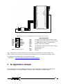
1
No.
1
2
3
4
5
6
7
8
9
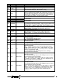
Function
AD7
AD6
AD5
AD4
AD3
AD2
AD1
AD0
A1
Alt. function
10
A0
11
12
SEL2
SEL1
13
PE7
INT7
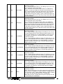
14
PE6
INT6
15
PE5
INT5
16
PE4
INT4
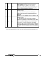
17
PE3
AC-
18
PE2
AC+
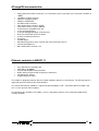
J1
Description
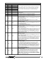
Data bus. Allows connecting externals peripherals mapped in
microcontroller address space. Peripheral addressing is done
with use of SEL1, SEL2 and/or A0, A1, #WR, #RD outputs.
Lowest two bits of address bus. Allows addressing 4 input and 4
output registers.
Note: outputs operate in 3.3V logic level standard.
Read/write strobe or address decoder outputs.
Note: outputs operate in 3.3V logic level standard.
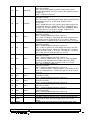
PE7 – General purpose digital I/O
Alternative functions:
INT7 – External Interrupt source 7: The PE7 pin can serve as an
external interrupt source.
IC3 – Input Capture Pin3: The PE7 pin can act as an input
capture pin for Timer/Counter3.
PE6 – general purpose digital I/O
Alternative functions:
INT6 – External Interrupt source 6: The PE6 pin can serve as an
external interrupt source.
T3 – Timer/Counter3 counter source.
PE5 – general purpose digital I/O
Alternative functions:
INT5 – External Interrupt source 5: The PE5 pin can serve as an
External Interrupt source.
OC3C – Output Compare Match C output: The PE5 pin can serve
as an External output for the Timer/Counter3 Output Compare C.
The pin has to be configured as an output (DDE5 set “one”) to
serve this function. The OC3C pin is also the output pin for the
PWM mode timer function.
PE4 – general purpose digital I/O
Alternative functions:
INT4 – External Interrupt source 4: The PE4 pin can serve as an
External Interrupt source.
OC3B – Output Compare Match B output: The PE4 pin can serve
as an External output for the Timer/Counter3 Output Compare B.
The pin has to be configured as an output (DDE4 set (one)) to
serve this function. The OC3B pin is also the output pin for the
PWM mode timer function.
PE3 – general purpose digital I/O
Alternative functions:
AC- – Analog Comparator Negative input. This pin is directly
connected to the negative input of the Analog Comparator.
OC3A, Output Compare Match A output: The PE3 pin can serve
as an External output for the Timer/Counter3 Output Compare A.
The pin has to be configured as an output (DDE3 set “one”) to
serve this function. The OC3A pin is also the output pin for the
PWM mode timer function.
PE2 – general purpose digital I/O
Alternative functions:
AC+ – Analog Comparator Positive input. This pin is directly
connected to the positive input of the Analog Comparator.
XCK0, USART0 External clock. The Data Direction Register
(DDE2) controls whether the clock is output (DDE2 set) or input
(DDE2 cleared). The XCK0 pin is active only when the USART0
operates in Synchronous mode.
8