1
LSPM2
ComDeC
4.4 Shift register interface
Besides the option of connecting an external EEPROM, the LSPM2 can also be wired with an external shift
register (XSREE=0). In this case, the integrated shift register controller independently generates control
sequences for shift registers with designation 74HC165 or compatible shift registers.
4.4.1 Shift register parameters
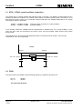
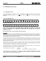
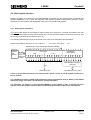
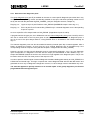
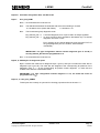
The internal shift register of the LSPM2 is written serially via bit position 23. The data are shifted to the right
depending on the number of clock pulses still pending, i.e. the contents of position 23 are stored in bit 22, and
the contents of position 22 are stored in bit 21 etc.
The following data sequence must be observed in this case at the serial data input (INTERDI):
first bit 0 (TS address) then bit 1 TS , bit 2 TS, bit 3 ...........bit 0 ID no, bit 1 ID no.,......etc.
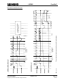
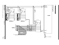
Shift direction of the internal shift register (LSPM2)
23 22 21 20 19 18 17 16 15 14 13 12 11 10 9 8 7 6 5 4 3 2 1 0
74HC165
external
shift
register
ID number
INTERDI
Serial
data input 7
LSPM2
6 5
High
4 3 2 1
Low
TS address
BCD-coded
0 7 6 5 4 3 2 1 0 7 6 5 4 3 2 1 0
BCD-BINARY convertor
(internal)
16
7
16 bit ID number
TS-Adresse, binary coded
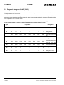
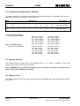
A total of 24 bits must be stored in the external shift register: 16 bits for the ID number and 8 bits for
the TS address.
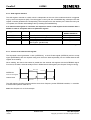
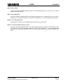
The TS address must be set BCD-coded externally (values permitted are 1Dec to 99Dec). If the LSPM2
detects the illegal value 0Dec, the TS address is assigned 126Dec.
The externally set address is converted BCD-BINARY in the LSPM2 in order to permit the Slave
address (TS) to be compared with the binary-coded destination address (DA) of the call telegram.
User Description
Copyright (C) Siemens AG 2002. All rights reserved.
Release V2.0
Page 17
10/2002