1
SAFETY PRECAUTIONS
(Read these precautions before using this product.)
Before using this product, please read this manual and the relevant manuals carefully and pay full attention
to safety to handle the product correctly.
The precautions given in this manual are concerned with this product only. For the safety precautions of the
programmable controller system, refer to the user's manual for the CPU module used.
In this manual, the safety precautions are classified into two levels: "
WARNING" and "
CAUTION".
WARNING
Indicates that incorrect handling may cause hazardous conditions,
resulting in death or severe injury.
CAUTION
Indicates that incorrect handling may cause hazardous conditions,
resulting in minor or moderate injury or property damage.
Under some circumstances, failure to observe the precautions given under "
CAUTION" may lead to
serious consequences.
Observe the precautions of both levels because they are important for personal and system safety.
Make sure that the end users read this manual and then keep the manual in a safe place for future
reference.
[Design Precautions]
WARNING
● Analog outputs may remain on due to a failure of the module. Configure an external interlock circuit
for output signals that could cause a serious accident.
● Do not write any data to the "system area" and "write-protect area" (R) of the buffer memory in the
intelligent function module.
Also, do not use any "use prohibited" signals as an output signal from the programmable controller
CPU to the intelligent function module.
Doing so may cause malfunction of the programmable controller system.
[Design Precautions]
CAUTION
● Do not install the control lines or communication cables together with the main circuit lines or power
cables.
Keep a distance of 100mm or more between them. Failure to do so may result in malfunction due to
noise.
● At power-on, a voltage may occur or a current may flow between output terminals for a moment. In
this case, start the control after analog outputs become stable.
● Power on or off the external power supply while the programmable controller is on. Failure to do so
may result in incorrect output or malfunction.
1
[Installation Precautions]
WARNING
● Shut off the external power supply for the system in all phases before connecting or removing a
module. Failure to do so may result in electric shock or cause the module to fail or malfunction.
[Installation Precautions]
CAUTION
● Use the programmable controller in an environment that meets the general specifications in the
manual "Safety Guidelines", the manual supplied with the CPU module or head module. Failure to
do so may result in electric shock, fire, malfunction, or damage to or deterioration of the product.
● To interconnect modules, engage the respective connectors and securely lock the module joint
levers. Incorrect interconnection may cause malfunction, failure, or drop of the module.
● Tighten the screw within the specified torque range.
Undertightening can cause drop of the screw, short circuit or malfunction.
Overtightening can damage the screw and/or module, resulting in drop, short circuit, or malfunction.
● Do not directly touch any conductive parts and electronic components of the module. Doing so can
cause malfunction or failure of the module.
[Wiring Precautions]
WARNING
● After installation and wiring, attach the included terminal cover to the module before turning it on for
operation. Failure to do so may result in electric shock.
[Wiring Precautions]
CAUTION
● Ground the FG terminal to the protective ground conductor dedicated to the programmable
controller. Failure to do so may result in electric shock or malfunction.
● Tighten the terminal block screw within the specified torque range. Undertightening can cause short
circuit, fire, or malfunction.
Overtightening can damage the screw and/or module, resulting in drop, short circuit, fire, or
malfunction.
● Prevent foreign matter such as dust or wire chips from entering the module. Such foreign matter can
cause a fire, failure, or malfunction.
● A protective film is attached to the top of the module to prevent foreign matter, such as wire chips,
from entering the module during wiring. Do not remove the film during wiring. Remove it for heat
dissipation before system operation.
2
[Wiring Precautions]
CAUTION
● Mitsubishi programmable controllers must be installed in control panels. Connect the main power
supply to the power supply module in the control panel through a relay terminal block.
Wiring and replacement of a power supply module must be performed by qualified maintenance
personnel with knowledge of protection against electric shock.
For wiring methods, refer to the MELSEC-L CPU Module User's Manual (Hardware Design,
Maintenance and Inspection).
[Startup and Maintenance Precautions]
WARNING
● Do not touch any terminal while power is on. Doing so will cause electric shock or malfunction.
● Shut off the external power supply for the system in all phases before cleaning the module or
retightening the terminal block screw. Failure to do so may result in electric shock.
[Startup and Maintenance Precautions]
CAUTION
● Do not disassemble or modify the module. Doing so may cause failure, malfunction, injury, or a fire.
● Shut off the external power supply for the system in all phases before connecting or removing a
module. Failure to do so may cause the module to fail or malfunction.
● Tighten the terminal block screw within the specified torque range. Undertightening can cause drop
of the component or wire, short circuit, or malfunction. Overtightening can damage the screw and/or
module, resulting in drop, short circuit, or malfunction.
● After the first use of the product (module, display unit, and terminal block), the number of
connections/disconnections is limited to 50 times (in accordance with IEC 61131-2). Exceeding the
limit may cause malfunction.
● Before handling the module, touch a conducting object such as a grounded metal to discharge the
static electricity from the human body. Failure to do so may cause the module to fail or malfunction.
[Disposal Precautions]
CAUTION
● When disposing of this product, treat it as industrial waste.
3
.
CONDITIONS OF USE FOR THE PRODUCT
(1) Mitsubishi programmable controller ("the PRODUCT") shall be used in conditions;
i) where any problem, fault or failure occurring in the PRODUCT, if any, shall not lead to any major
or serious accident; and
ii) where the backup and fail-safe function are systematically or automatically provided outside of
the PRODUCT for the case of any problem, fault or failure occurring in the PRODUCT.
(2) The PRODUCT has been designed and manufactured for the purpose of being used in general
industries.
MITSUBISHI SHALL HAVE NO RESPONSIBILITY OR LIABILITY (INCLUDING, BUT NOT
LIMITED TO ANY AND ALL RESPONSIBILITY OR LIABILITY BASED ON CONTRACT,
WARRANTY, TORT, PRODUCT LIABILITY) FOR ANY INJURY OR DEATH TO PERSONS OR
LOSS OR DAMAGE TO PROPERTY CAUSED BY the PRODUCT THAT ARE OPERATED OR
USED IN APPLICATION NOT INTENDED OR EXCLUDED BY INSTRUCTIONS, PRECAUTIONS,
OR WARNING CONTAINED IN MITSUBISHI'S USER, INSTRUCTION AND/OR SAFETY
MANUALS, TECHNICAL BULLETINS AND GUIDELINES FOR the PRODUCT.
("Prohibited Application")
Prohibited Applications include, but not limited to, the use of the PRODUCT in;
• Nuclear Power Plants and any other power plants operated by Power companies, and/or any
other cases in which the public could be affected if any problem or fault occurs in the PRODUCT.
• Railway companies or Public service purposes, and/or any other cases in which establishment of
a special quality assurance system is required by the Purchaser or End User.
• Aircraft or Aerospace, Medical applications, Train equipment, transport equipment such as
Elevator and Escalator, Incineration and Fuel devices, Vehicles, Manned transportation,
Equipment for Recreation and Amusement, and Safety devices, handling of Nuclear or
Hazardous Materials or Chemicals, Mining and Drilling, and/or other applications where there is a
significant risk of injury to the public or property.
Notwithstanding the above, restrictions Mitsubishi may in its sole discretion, authorize use of the
PRODUCT in one or more of the Prohibited Applications, provided that the usage of the PRODUCT
is limited only for the specific applications agreed to by Mitsubishi and provided further that no
special quality assurance or fail-safe, redundant or other safety features which exceed the general
specifications of the PRODUCTs are required. For details, please contact the Mitsubishi
representative in your region.
4
INTRODUCTION
Thank you for purchasing the Mitsubishi MELSEC-L series programmable controllers.
This manual describes the functions and programming of a digital-analog converter module (hereafter abbreviated as
D/A converter module).
Before using this product, please read this manual and the relevant manuals carefully and develop familiarity with the
functions and performance of the MELSEC-L series programmable controller to handle the product correctly.
When applying the program examples introduced in this manual to the actual system, ensure the applicability and
confirm that it will not cause system control problems.
Relevant module: L60DA4
Remark
Unless otherwise specified, this manual describes the program examples in which the I/O numbers of X/Y00 to
X/Y0F are assigned for a D/A converter module.
For I/O number assignment, refer to the following.
MELSEC-L CPU Module User's Manual (Function Explanation, Program Fundamentals)
Operating procedures are explained using GX Works2. When using GX Developer or GX Configurator-DA, refer to the
following.
• When using GX Developer or GX Configurator-DA (
Page 125, Appendix 8)
5
COMPLIANCE WITH THE EMC AND LOW VOLTAGE
DIRECTIVES
(1) For programmable controller system
To configure a system meeting the requirements of the EMC and Low Voltage Directives when incorporating the
Mitsubishi programmable controller (EMC and Low Voltage Directives compliant) into other machinery or
equipment, refer to the manual "Safety Guidelines", the manual supplied with the CPU module or head module.
The CE mark, indicating compliance with the EMC and Low Voltage Directives, is printed on the rating plate of the
programmable controller.
(2) For the product
No additional measures are necessary for the compliance of this product with the EMC and Low Voltage
Directives.
6
RELEVANT MANUALS
(1) CPU module user's manual
Manual name
Description
<manual number (model code)>
MELSEC-L CPU Module User's Manual (Hardware Design,
Maintenance and Inspection)
<SH-080890ENG, 13JZ36>
Specifications of the CPU modules, power supply modules, display
unit, SD memory cards, and batteries, information on how to
establish a system, maintenance and inspection, and
troubleshooting
MELSEC-L CPU Module User's Manual (Function Explanation,
Program Fundamentals)
Functions and devices of the CPU module, and programming
<SH-080889ENG, 13JZ35>
(2) Head module user's manual
Manual name
Description
<manual number (model code)>
MELSEC-L CC-Link IE Field Network Head Module User's Manual
<SH-080919ENG, 13JZ48>
Specifications for a head module, procedures before operation,
system configuration, installation and wiring, settings, and
troubleshooting
MELSEC-Q CC-Link IE Field Network Master/Local Module User's
Specifications for master/local module, procedures before operation,
Manual
system configuration, installation, settings, functions, programming,
<SH-080917ENG, 13JZ47>
and troubleshooting
(3) Operating manual
Manual name
<manual number (model code)>
GX Works2 Version1 Operating Manual (Common)
<SH-080779ENG, 13JU63>
GX Developer Version 8 Operating Manual
Description
System configuration, parameter settings, and online operations
(common to Simple project and Structured project) of GX Works2
Operating methods of GX Developer, such as programming,
<SH-080373E, 13JU41>
printing, monitoring, and debugging
7
CONTENTS
CONTENTS
SAFETY PRECAUTIONS . . . . . . . . . . . . . . . . . . . . . . . . . . . . . . . . . . . . . . . . . . . . . . . . . . . . . . . . . . . . . 1
CONDITIONS OF USE FOR THE PRODUCT . . . . . . . . . . . . . . . . . . . . . . . . . . . . . . . . . . . . . . . . . . . . . 4
INTRODUCTION . . . . . . . . . . . . . . . . . . . . . . . . . . . . . . . . . . . . . . . . . . . . . . . . . . . . . . . . . . . . . . . . . . . . 5
COMPLIANCE WITH THE EMC AND LOW VOLTAGE DIRECTIVES . . . . . . . . . . . . . . . . . . . . . . . . . . . 6
RELEVANT MANUALS . . . . . . . . . . . . . . . . . . . . . . . . . . . . . . . . . . . . . . . . . . . . . . . . . . . . . . . . . . . . . . . 7
MANUAL PAGE ORGANIZATION . . . . . . . . . . . . . . . . . . . . . . . . . . . . . . . . . . . . . . . . . . . . . . . . . . . . . . 11
TERMS . . . . . . . . . . . . . . . . . . . . . . . . . . . . . . . . . . . . . . . . . . . . . . . . . . . . . . . . . . . . . . . . . . . . . . . . . . 14
PACKING LIST . . . . . . . . . . . . . . . . . . . . . . . . . . . . . . . . . . . . . . . . . . . . . . . . . . . . . . . . . . . . . . . . . . . . 14
CHAPTER 1 D/A CONVERTER MODULE
1.1
Application . . . . . . . . . . . . . . . . . . . . . . . . . . . . . . . . . . . . . . . . . . . . . . . . . . . . . . . . . . . . . . . . 15
1.2
Features . . . . . . . . . . . . . . . . . . . . . . . . . . . . . . . . . . . . . . . . . . . . . . . . . . . . . . . . . . . . . . . . . . 16
CHAPTER 2 PART NAMES
17
CHAPTER 3 SPECIFICATIONS
19
3.1
General Specifications . . . . . . . . . . . . . . . . . . . . . . . . . . . . . . . . . . . . . . . . . . . . . . . . . . . . . . . 19
3.2
Performance Specifications . . . . . . . . . . . . . . . . . . . . . . . . . . . . . . . . . . . . . . . . . . . . . . . . . . . 20
3.2.1
Number of parameter settings . . . . . . . . . . . . . . . . . . . . . . . . . . . . . . . . . . . . . . . . . . . . . . . .21
3.3
Function List . . . . . . . . . . . . . . . . . . . . . . . . . . . . . . . . . . . . . . . . . . . . . . . . . . . . . . . . . . . . . . . 22
3.4
I/O Signal List . . . . . . . . . . . . . . . . . . . . . . . . . . . . . . . . . . . . . . . . . . . . . . . . . . . . . . . . . . . . . . 23
3.5
Buffer Memory List . . . . . . . . . . . . . . . . . . . . . . . . . . . . . . . . . . . . . . . . . . . . . . . . . . . . . . . . . . 24
CHAPTER 4 PROCEDURES BEFORE STARTING THE OPERATION
29
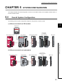
CHAPTER 5 SYSTEM CONFIGURATION
31
5.1
Overall System Configuration . . . . . . . . . . . . . . . . . . . . . . . . . . . . . . . . . . . . . . . . . . . . . . . . . . 31
5.2
Applicable System . . . . . . . . . . . . . . . . . . . . . . . . . . . . . . . . . . . . . . . . . . . . . . . . . . . . . . . . . . 32
5.3
Restrictions When D/A Converter Module is Connected to Head Module . . . . . . . . . . . . . . . . 32
CHAPTER 6 INSTALLATION AND WIRING
33
6.1
Installation Environment and Installation Position . . . . . . . . . . . . . . . . . . . . . . . . . . . . . . . . . . 33
6.2
Terminal Block . . . . . . . . . . . . . . . . . . . . . . . . . . . . . . . . . . . . . . . . . . . . . . . . . . . . . . . . . . . . . 34
6.3
Wiring . . . . . . . . . . . . . . . . . . . . . . . . . . . . . . . . . . . . . . . . . . . . . . . . . . . . . . . . . . . . . . . . . . . . 36
6.4
External Wiring . . . . . . . . . . . . . . . . . . . . . . . . . . . . . . . . . . . . . . . . . . . . . . . . . . . . . . . . . . . . . 37
CHAPTER 7 VARIOUS SETTINGS
8
15
38
7.1
Addition of Modules . . . . . . . . . . . . . . . . . . . . . . . . . . . . . . . . . . . . . . . . . . . . . . . . . . . . . . . . . 38
7.2
Switch Setting . . . . . . . . . . . . . . . . . . . . . . . . . . . . . . . . . . . . . . . . . . . . . . . . . . . . . . . . . . . . . . 39
7.3
Parameter Setting. . . . . . . . . . . . . . . . . . . . . . . . . . . . . . . . . . . . . . . . . . . . . . . . . . . . . . . . . . . 40
7.4
Auto Refresh. . . . . . . . . . . . . . . . . . . . . . . . . . . . . . . . . . . . . . . . . . . . . . . . . . . . . . . . . . . . . . . 41
7.5
Offset/Gain Setting . . . . . . . . . . . . . . . . . . . . . . . . . . . . . . . . . . . . . . . . . . . . . . . . . . . . . . . . . . 42
7.5.1
Setting from GX Works2 "Offset/Gain Setting" . . . . . . . . . . . . . . . . . . . . . . . . . . . . . . . . . . .42
7.5.2
Setting from a program . . . . . . . . . . . . . . . . . . . . . . . . . . . . . . . . . . . . . . . . . . . . . . . . . . . . .45
CHAPTER 8 FUNCTIONS
49
8.1
D/A Conversion Enable/Disable Function. . . . . . . . . . . . . . . . . . . . . . . . . . . . . . . . . . . . . . . . . 49
8.2
D/A Output Enable/Disable Function . . . . . . . . . . . . . . . . . . . . . . . . . . . . . . . . . . . . . . . . . . . . 49
8.3
Analog Output HOLD/CLEAR Function . . . . . . . . . . . . . . . . . . . . . . . . . . . . . . . . . . . . . . . . . . 50
8.4
Analog Output Test when CPU Module is in STOP Status . . . . . . . . . . . . . . . . . . . . . . . . . . . . 52
8.5
Scaling Function . . . . . . . . . . . . . . . . . . . . . . . . . . . . . . . . . . . . . . . . . . . . . . . . . . . . . . . . . . . . 54
8.6
Alarm Output Function . . . . . . . . . . . . . . . . . . . . . . . . . . . . . . . . . . . . . . . . . . . . . . . . . . . . . . . 59
8.7
Error Log Function . . . . . . . . . . . . . . . . . . . . . . . . . . . . . . . . . . . . . . . . . . . . . . . . . . . . . . . . . . 61
8.8
Module Error Collection Function . . . . . . . . . . . . . . . . . . . . . . . . . . . . . . . . . . . . . . . . . . . . . . . 63
8.9
Error Clear Function . . . . . . . . . . . . . . . . . . . . . . . . . . . . . . . . . . . . . . . . . . . . . . . . . . . . . . . . . 64
8.10
Saving and Restoring Offset/Gain Values . . . . . . . . . . . . . . . . . . . . . . . . . . . . . . . . . . . . . . . . 65
CHAPTER 9 DISPLAY UNIT
70
9.1
Display Unit. . . . . . . . . . . . . . . . . . . . . . . . . . . . . . . . . . . . . . . . . . . . . . . . . . . . . . . . . . . . . . . . 70
9.2
Menu Structure . . . . . . . . . . . . . . . . . . . . . . . . . . . . . . . . . . . . . . . . . . . . . . . . . . . . . . . . . . . . . 70
9.3
List of Setting Value Change Screens . . . . . . . . . . . . . . . . . . . . . . . . . . . . . . . . . . . . . . . . . . . 72
9.4
Checking and Clearing Errors. . . . . . . . . . . . . . . . . . . . . . . . . . . . . . . . . . . . . . . . . . . . . . . . . . 75
CHAPTER 10 PROGRAMMING
77
10.1
Procedure for Programming . . . . . . . . . . . . . . . . . . . . . . . . . . . . . . . . . . . . . . . . . . . . . . . . . . . 77
10.2
When Using a Standard System Configuration . . . . . . . . . . . . . . . . . . . . . . . . . . . . . . . . . . . . 78
10.3
When D/A Converter Module is Connected to Head Module . . . . . . . . . . . . . . . . . . . . . . . . . . 83
CHAPTER 11 TROUBLESHOOTING
90
11.1
Checking on the Module Detailed Information . . . . . . . . . . . . . . . . . . . . . . . . . . . . . . . . . . . . . 91
11.2
Checking by Latest Error Code (Un\G19). . . . . . . . . . . . . . . . . . . . . . . . . . . . . . . . . . . . . . . . . 92
11.3
Checking on the Module Error Collection Function . . . . . . . . . . . . . . . . . . . . . . . . . . . . . . . . . 92
11.4
Error Code List . . . . . . . . . . . . . . . . . . . . . . . . . . . . . . . . . . . . . . . . . . . . . . . . . . . . . . . . . . . . . 93
11.5
Alarm Code List . . . . . . . . . . . . . . . . . . . . . . . . . . . . . . . . . . . . . . . . . . . . . . . . . . . . . . . . . . . . 94
11.6
Troubleshooting . . . . . . . . . . . . . . . . . . . . . . . . . . . . . . . . . . . . . . . . . . . . . . . . . . . . . . . . . . . . 95
11.7
Checking the Status of D/A Converter Module by the System Monitor . . . . . . . . . . . . . . . . . . 97
APPENDICES
98
Appendix 1 Details of I/O Signals . . . . . . . . . . . . . . . . . . . . . . . . . . . . . . . . . . . . . . . . . . . . . . . . . . . . 98
Appendix 1.1 Input Signal . . . . . . . . . . . . . . . . . . . . . . . . . . . . . . . . . . . . . . . . . . . . . . . . . . . . . . . . . .98
Appendix 1.2 Output Signal. . . . . . . . . . . . . . . . . . . . . . . . . . . . . . . . . . . . . . . . . . . . . . . . . . . . . . . .102
Appendix 2 Details of Buffer Memory Addresses . . . . . . . . . . . . . . . . . . . . . . . . . . . . . . . . . . . . . . . 104
Appendix 3 I/O Conversion Characteristic of D/A Conversion . . . . . . . . . . . . . . . . . . . . . . . . . . . . . 112
Appendix 4 D/A Conversion Accuracy. . . . . . . . . . . . . . . . . . . . . . . . . . . . . . . . . . . . . . . . . . . . . . . . 114
Appendix 5 Dedicated Instruction . . . . . . . . . . . . . . . . . . . . . . . . . . . . . . . . . . . . . . . . . . . . . . . . . . . 115
Appendix 5.1 Instruction List . . . . . . . . . . . . . . . . . . . . . . . . . . . . . . . . . . . . . . . . . . . . . . . . . . . . . . . 115
Appendix 5.2 G(P).OFFGAN . . . . . . . . . . . . . . . . . . . . . . . . . . . . . . . . . . . . . . . . . . . . . . . . . . . . . . . 116
9
Appendix 5.3 G(P).OGLOAD. . . . . . . . . . . . . . . . . . . . . . . . . . . . . . . . . . . . . . . . . . . . . . . . . . . . . . . 118
Appendix 5.4 G(P).OGSTOR . . . . . . . . . . . . . . . . . . . . . . . . . . . . . . . . . . . . . . . . . . . . . . . . . . . . . .121
Appendix 6 Checking Serial Number and Function Version . . . . . . . . . . . . . . . . . . . . . . . . . . . . . . . 124
Appendix 7 Differences with Q Series . . . . . . . . . . . . . . . . . . . . . . . . . . . . . . . . . . . . . . . . . . . . . . . . 124
Appendix 8 When Using GX Developer or GX Configurator-DA . . . . . . . . . . . . . . . . . . . . . . . . . . . . 125
Appendix 8.1 Operation of GX Developer . . . . . . . . . . . . . . . . . . . . . . . . . . . . . . . . . . . . . . . . . . . . .125
Appendix 8.2 Operation of GX Configurator-DA . . . . . . . . . . . . . . . . . . . . . . . . . . . . . . . . . . . . . . . .127
Appendix 9 External Dimensions. . . . . . . . . . . . . . . . . . . . . . . . . . . . . . . . . . . . . . . . . . . . . . . . . . . . 129
INDEX
131
INSTRUCTION INDEX
133
REVISIONS . . . . . . . . . . . . . . . . . . . . . . . . . . . . . . . . . . . . . . . . . . . . . . . . . . . . . . . . . . . . . . . . . . . . . . 134
Warranty . . . . . . . . . . . . . . . . . . . . . . . . . . . . . . . . . . . . . . . . . . . . . . . . . . . . . . . . . . . . . . . . . . . . . . . . 135
10
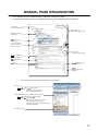
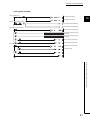
MANUAL PAGE ORGANIZATION
In this manual, pages are organized and the symbols are used as shown below.
The following page illustration is for explanation purpose only, and is different from the actual pages.
"" is used for
screen names and items.
The chapter of
the current page is shown.
shows operating
procedures.
shows mouse
operations.*1
[ ] is used for items
in the menu bar and
the project window.
The section of
the current page is shown.
Ex. shows setting or
operating examples.
shows reference
manuals.
shows notes that
requires attention.
shows
reference pages.
shows useful
information.
*1
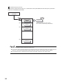
The mouse operation example is provided below. (For GX Works2)
Menu bar
Ex.
[Online]
[Write to PLC...]
Select [Online] on the menu bar,
and then select [Write to PLC...].
A window selected in the view selection area is displayed.
Ex.
[Parameter]
Project window
[PLC Parameter]
Select [Project] from the view selection
area to open the Project window.
In the Project window, expand [Parameter] and
select [PLC Parameter].
View selection area
11
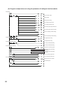
Pages describing instructions are organized as shown below.
The following page illustrations are for explanation purpose only, and are different from the actual pages.
Instruction name
Execution condition of the instruction
Structure of the instruction
in the ladder mode
shows the devices
applicable to the instruction
Descriptions of
setting data and data type
Descriptions of
control data (if any)
Detailed descriptions
of the instruction
Conditions for the error and
error codes
For the errors not described in
this manual, refer to the following.
MELSEC-Q/L Programming
Manual (Common Instruction)
Simple program example(s)
and descriptions of the devices used
12
Setting side
User : Device value is set by the user.
System: Device value is set by
the CPU module.
• Instructions can be executed under the following conditions.
Execution condition
Any time
Symbol
No symbol
On the rising
During on
edge
During off
On the falling
edge
• The following devices can be used.
Internal device
Setting
(system, user)
data
Applicable
device *1
Bit
Word
X, Y, M, L,
SM, F, B,
SB, FX,
FY*2
T, ST, C, D,
W, SD,
SW, FD,
Link direct device
Intelligent
J\
function module
File
register
Bit
R, ZR
Word
⎯
device
U\G
U\G
Index
register
Zn
Z
@
*1
For details on each device, refer to the following.
*2
*3
MELSEC-L CPU Module User's Manual (Function Explanation, Program Fundamentals)
FX and FY can be used for bit data only, and FD for word data only.
In the "Constant" and "Others" columns, a device(s) that can be set for each instruction is shown.
Con-
Others
stant *3
*3
K, H, E, $
P, I, J, U,
D, X, DY,
N, BL, TR,
BL\S, V
• The following data types can be used.
Data type
Description
Bit
Bit data or the start number of bit data
BIN 16-bit
16-bit binary data or the start number of word device
BIN 32-bit
32-bit binary data or the start number of double-word device
BCD 4-digit
Four-digit binary-coded decimal data
BCD 8-digit
Eight-digit binary-coded decimal data
Real number
Floating-point data
Character string
Character string data
Device name
Device name data
13
TERMS
Unless otherwise specified, this manual uses the following terms.
Term
Description
D/A converter module
Another term for the MELSEC-L series digital-analog converter module
Head module
Abbreviation for the LJ72GF15-T2 CC-Link IE field network head module
Display unit
A liquid crystal display to be attached to the CPU module
Programming tool
Generic term for GX Works2 and GX Developer
Factory default setting
Generic term for analog output ranges of 0 to 5V, 1 to 5V, -10 to 10V, 0 to 20mA, and 4 to 20mA
GX Works2
GX Developer
GX Configurator-DA
Buffer memory
Product name of the software package for the MELSEC programmable controllers
A setting and monitoring tool added in GX Developer (for D/A converter modules)
The memory of an intelligent function module used to store data (such as setting values and monitored
values) for communication with a CPU module.
PACKING LIST
The following items are included in the package of this product. Before use, check that all the items are included.
L60DA4
L60DA4
14
Before Using the Product
CHAPTER 1 D/A CONVERTER MODULE
CHAPTER 1
D/A CONVERTER MODULE
1
This chapter describes the application and features of the D/A converter module.
1.1
Application
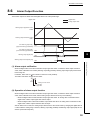
This module converts the digital data received from the CPU module to the analog signal and outputs the signal to
external devices. By converting the data, which has been processed through the CPU module, to an analog data, the
input information can be sent to the devices including an inverter.
Digital to analog
conversion
Analog signal (continuous signal)
Digital signal (discrete signal)
The D/A converter module enables works as follows.
Connect the module to the control valve to control the flow to
Connect the module to an inverter to control the conveyer
a tank.
belt speed.
Flow control
1.1 Application
Control valve
Inverter
Conveyer
Tank
Connect the module to the power conditioning equipment to
control the heating temperature of a heater or others.
Power conditioner
Heater
15
1.2
Features
(1) Improved response by high-speed conversion
The high-speed conversion speed of 20µs/channel is achieved.
(2) Detailed control by high resolution
In all analog output ranges, the high resolution of 1/20000 is achieved.
(3) Reliability by high accuracy
The accuracy for the maximum value of analog output value is ± 0.1% (25 ± 5°C) and ± 0.3% (0 to 55°C).
(4) Scaling function
This function converts a digital value to the ratio value (%) in any width to represent the digital value in a numeric
value easy to understand.
(5) Error detection and monitoring
When the digital value exceeds the specified range, the module detects an alarm so that the digital value error
monitoring and the output control are enabled.
16
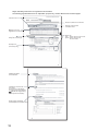
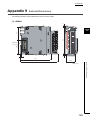
CHAPTER 2 PART NAMES
CHAPTER 2
PART NAMES
2
The following table shows the part names of the D/A converter module.
1)
1)
2)
4)
3)
7)
6)
5)
1)
Number
1)
8)
1)
Name
Module joint levers
Description
Levers for connecting two modules
Displays the operating status of the D/A converter module.
2)
On: The module is operating normally.
RUN LED (green)
Flashing: In the offset/gain setting mode
Off: The 5V power off or watchdog timer error has occurred.
Displays the errors and status of the D/A converter module.
3)
On: an error has occurred except for error code: 112*1
ERR. LED (red)
Flashing: Error code: 112 has occurred.*1
Off : during normal operation
Displays the alarm status of the D/A converter module.
4)
On: Alarm output is occurring*2
ALM LED (red)
Off: The module is operating normally.*2
5)
DIN rail hook
6)
Terminal block
7)
Terminal block cover
Cover for preventing electric shock while the power is on.
8)
Serial number display
Displays the serial number printed on the rating plate.
*1
Error Code List (
*2
Alarm Code List (
A hook used to mount the module to a DIN rail
18-pin screw terminal block for connecting output signal lines of such as
external devices
Page 93, Section 11.4)
Page 94, Section 11.5)
17
Memo
18
CHAPTER 3 SPECIFICATIONS
CHAPTER 3
SPECIFICATIONS
This chapter describes general specifications, performance specifications, function list, list of I/O signals, and list of
buffer memory addresses.
3.1
3
General Specifications
For the general specifications of the D/A converter module, refer to the following.
The manual "Safety Guidelines", the manual supplied with the CPU module or head module
3.1 General Specifications
19
3.2
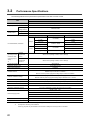
Performance Specifications
The following table shows the performance specifications of the D/A converter module.
Model
Item
L60DA4
Number of analog output points
4 points (4 channels)
Digital input
-20480 to 20479
When using the
-32768 to 32767
scaling function
Analog output
Voltage
-10 to 10 VDC (external load resistance 1kΩ to 1MΩ)
Current
0 to 20 mADC (external load resistance 0Ω to 600Ω))
Analog output range
Digital value
0 to 5V
Voltage
I/O characteristics, resolution
0 to 20000
1 to 5V
-10 to 10V
User range setting
0 to 20mA
Current
Ambient
(accuracy for the
temperature
maximum value
25±5°C
of analog output
Ambient
value)
temperature
*2
0 to 55°C
Conversion speed
-20000 to 20000
0 to 20000
4 to 20mA
User range setting
Accuracy
Resolution
-20000 to 20000
250µV
200µV
500µV
333µV*1
1000nA
800nA
700nA*1
Within ±0.1% (voltage: ±10mV, current: ±20µA)
Within ±0.3% (voltage: ±30mV, current: ±60µA)
20µs/channel
Offset/gain setting count
Output short protection
Up to 50000 counts
Protected
Between I/O terminals and programmable controller power supply: photocoupler isolation
Isolation method
Between output channels: no isolation
Between external power supply and analog output: transformer isolation
Dielectric withstand voltage
Insulation resistance
Number of occupied I/O points
Between I/O terminals and programmable controller power supply: 500VACrms for 1 minute
Between external power supply and analog output: 500VACrms for 1 minute
Between I/O terminals and programmable controller power supply: 500VDC 10MΩ or higher
16 points (I/O assignment: Intelligent 16 points)
Connected terminal
18-point terminal block
Applicable wire size
0.3 to 0.75mm2
Applicable solderless terminal
R1.25 to 3 (solderless terminals with sleeve are not usable)
24VDC +20%, -15%
External supply power
Ripple, spike 500mVP-P or lower
Inrush current: 4.3A, 1000µs or shorter
Current consumption: 0.18A
Internal current consumption (5VDC)
0.16A
Weight
0.20kg
*1
*2
20
Maximum resolution in the user range setting.
Except when receiving noise influence.
Warm up (or power on) the module for 30 minutes to satisfy the accuracy shown in the table.
CHAPTER 3 SPECIFICATIONS
3.2.1
Number of parameter settings
Set the initial setting of D/A converter module and the parameter setting of auto refresh setting so that the number of
parameters, including these of other intelligent function modules, does not exceed the number of parameters that can
be set in the CPU module or the head module.
For the maximum number of parameters that can be set in the CPU module or the head module (maximum number of
parameter settings), refer to the following.
3
MELSEC-L CPU Module User's Manual (Hardware Design, Maintenance and Inspection)
MELSEC-L CC-Link IE Field Network Head Module User's Manual
(1) Number of the D/A converter module parameters
For D/A converter modules, the following number of parameters can be set per module.
Target module
Initial setting
Auto refresh setting
4
11 (maximum number of settings)
L60DA4
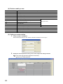
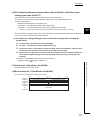
(2) Checking method
The maximum number of parameter settings and the number of parameter settings set for the intelligent function
module can be checked with the following operation.
Project window
[Intelligent Function Module]
Right-click
[Intelligent Function Module Parameter List]
3.2 Performance Specifications
3.2.1 Number of parameter settings
1)
No.
2)
3)
4)
Description
1)
The total number of parameters in the initial settings selected on the dialog box
2)
The maximum number of parameter settings in the initial settings
3)
The total number of parameters in the auto refresh settings selected on the dialog box
4)
The maximum number of parameter settings in the auto refresh settings
21
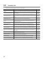
3.3
Function List
The following shows the function list of the D/A converter module.
Item
Description
D/A conversion enable/disable
Sets whether to enable or disable D/A conversion for each channel.
function
Disabling the D/A conversion for unused channels reduces the conversion cycles.
This function sets whether to output the D/A conversion value or the offset value,
D/A output enable/disable function
for each channel.
The conversion speed is constant, regardless of the output enable/disable status.
The output range to use can be selected from the factory default range (4mA to
Range switching function
20mA, 0mA to20mA, 1V to 5V, 0V to 5V or -10V to 10V) and user range (user range
setting).
Offset/gain setting function
Analog output HOLD/CLEAR
function
This function compensates for errors in analog output values.
This function sets whether to hold the output analog value (HOLD) or clear the
output analog value (CLEAR), according to the CPU module operating status
(RUN, STOP or stop error).
Analog output test when CPU
When the CPU module is in STOP operation status, forcibly turning CH Output
module is in STOP status
enable/disable flag (Y1 to Y4) ON outputs the D/A-converted analog value.
This function performs a scale conversion of the digital value that was input into a
Scaling function
digital value between -20000 and 20000 (or 0 and 20000) using any given set
scaling upper or lower limit value, and outputs the corresponding analog value.
Alarm output function
External power supply READY flag
(X7)
Error log function
Module error collection
This function outputs an alarm when the digital value is outside the preset range.
Page 49,
Section 8.1
Page 49,
Section 8.2
Page 39,
Section 7.2
Page 42,
Section 7.5
Page 50,
Section 8.3
Page 52,
Section 8.4
Page 54,
Section 8.5
Page 59,
Section 8.6
This signal turns ON when the external power supply 24VDC is supplied.
Page 98,
When the flag is OFF, 0V/0mA are output to analog output values regardless of
Appendix
other settings.
This function stores up to 16 errors and alarms that occur on the D/A converter
module to the buffer memory as history.
This function collects errors and alarms occurred in the D/A converter module and
stores to the CPU module or the head module.
Error clear function
Clearing the error from the system monitor at error occurrence is possible.
Save/restoration of offset/gain value
The offset/gain value of the user range setting can be saved or restored.
22
Reference
1.1(2)
Page 61,
Section 8.7
Page 63,
Section 8.8
Page 64,
Section 8.9
Page 65,
Section 8.10
CHAPTER 3 SPECIFICATIONS
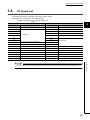
3.4
I/O Signal List
The following shows the I/O signal list of the D/A converter module.
For details on the setting status, refer to the following.
• Details of I/O signals (
Page 98, Appendix 1)
Input signal
Device number
X0
Signal name
Device number
Y0
Use prohibited
Y1
CH1 Output enable/disable flag
X2
Y2
CH2 Output enable/disable flag
X3
Y3
CH3 Output enable/disable flag
Y4
CH4 Output enable/disable flag
Use prohibited
X5
Y5
X6
Y6
3
Signal name
X1
X4
Module READY
Output signal
Use prohibited
X7
External power supply READY flag
Y7
X8
Use prohibited
Y8
X9
Operating condition setting completed flag
Y9
Operating condition setting request
XA
Offset/gain setting mode flag
YA
User range writing request
XB
Channel change completed flag
YB
Channel change request
XC
Set value change completed flag
YC
Set value change request
XD
Use prohibited
YD
Use prohibited
XE
Warning output signal
YE
Warning output clear request
XF
Error flag
YF
Error clear request
23
3.4 I/O Signal List
The I/O number (X/Y) described above shows the case that the start I/O number of the D/A converter module is set to "0".
3.5
Buffer Memory List
The following shows the buffer memory list of the D/A converter module.
For details on buffer memory, refer to the following.
• Detail of buffer memory (
Page 104, Appendix 2)
Do not write data to the system area and the area where the data cannot be written from the program in buffer memory.
Writing data to these areas may lead the module to malfunction.
(1) Un\G0 to Un\G1799
24
Address
Address
(decimal)
(hexadecimal)
0
0H
D/A conversion enable/disable setting
1
1H
2
2H
3
3H
4
4H
5
5H
to
to
10
AH
11
BH
12
Name
Default
Read/Write
*1
*2
000FH
R/W
CH1 Digital value
0
R/W
CH2 Digital value
0
R/W
CH3 Digital value
0
R/W
CH4 Digital value
0
R/W
System area
⎯
⎯
CH1 Set value check code
0000H
R
CH
CH2 Set value check code
0000H
R
13
DH
CH3 Set value check code
0000H
R
14
EH
CH4 Set value check code
0000H
R
15
FH
to
to
System area
⎯
⎯
18
12H
19
13H
Latest error code
0
R
20
14H
Setting range
0000H
R
21
15H
System area
⎯
⎯
22
16H
Offset/gain setting mode Offset specification
0000H
R/W
23
17H
Offset/gain setting mode Gain specification
0000H
R/W
24
18H
Offset/gain adjustment value specification
0
R/W
25
19H
System area
⎯
⎯
26
1AH
HOLD/CLEAR function setting
0000H
R
27
1BH
⎯
⎯
to
to
46
2EH
System area
47
2FH
Warning output setting
000FH
R/W
48
30H
Warning output flag
0000H
R
CHAPTER 3 SPECIFICATIONS
Address
Address
(decimal)
(hexadecimal)
49
31H
to
to
52
34H
53
35H
54
Default
Read/Write
*1
*2
⎯
⎯
Scaling enable/disable setting
000FH
R/W
36H
CH1 Scaling lower limit value
0
R/W
55
37H
CH1 Scaling upper limit value
0
R/W
56
38H
CH2 Scaling lower limit value
0
R/W
57
39H
CH2 Scaling upper limit value
0
R/W
58
3AH
CH3 Scaling lower limit value
0
R/W
59
3BH
CH3 Scaling upper limit value
0
R/W
60
3CH
CH4 Scaling lower limit value
0
R/W
61
3DH
CH4 Scaling upper limit value
0
R/W
62
3EH
to
to
System area
⎯
⎯
85
55H
86
56H
CH1 Warning output upper limit value
0
R/W
87
57H
CH1 Warning output lower limit value
0
R/W
88
58H
CH2 Warning output upper limit value
0
R/W
89
59H
CH2 Warning output lower limit value
0
R/W
90
5AH
CH3 Warning output upper limit value
0
R/W
91
5BH
CH3 Warning output lower limit value
0
R/W
92
5CH
CH4 Warning output upper limit value
0
R/W
93
5DH
CH4 Warning output lower limit value
0
R/W
94
5EH
to
to
System area
⎯
⎯
157
9DH
158
9EH
0
R/W
159
9FH
0
R/W
160
A0H
to
to
System area
⎯
⎯
199
C7H
200
C8H
Pass data classification setting
0
R/W
201
C9H
System area
⎯
⎯
202
CAH
CH1 Industrial shipment settings offset value
0
R/W
203
CBH
CH1 Industrial shipment settings gain value
0
R/W
204
CCH
CH2 Industrial shipment settings offset value
0
R/W
205
CDH
CH2 Industrial shipment settings gain value
0
R/W
206
CEH
CH3 Industrial shipment settings offset value
0
R/W
207
CFH
CH3 Industrial shipment settings gain value
0
R/W
208
D0H
CH4 Industrial shipment settings offset value
0
R/W
209
D1H
CH4 Industrial shipment settings gain value
0
R/W
210
D2H
CH1 User range settings offset value
0
R/W
Name
System area
3.5 Buffer Memory List
Mode switching setting
3
25
Address
Address
(decimal)
(hexadecimal)
211
D3H
212
Default
Read/Write
*1
*2
CH1 User range settings gain value
0
R/W
D4H
CH2 User range settings offset value
0
R/W
213
D5H
CH2 User range settings gain value
0
R/W
214
D6H
CH3 User range settings offset value
0
R/W
215
D7H
CH3 User range settings gain value
0
R/W
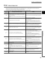
216
D8H
CH4 User range settings offset value
0
R/W
217
D9H
CH4 User range settings gain value
0
R/W
218
DAH
to
to
System area
⎯
⎯
1799
707H
*1
*2
26
Name
The default value is a value set after power-on or after resetting the CPU module.
This shows whether reading the data from or writing the data to the area with programs is possible.
R: Readable
W: Writable
CHAPTER 3 SPECIFICATIONS
(2) Error history (Un\G1800 to Un\G1969)
Address
Address
(decimal)
(hexadecimal)
1800
708H
1801
709H
to
to
1809
711H
1810
712H
1811
713H
714H
1813
715H
1814
716H
1815
717H
to
to
1819
71BH
1820
71CH
to
to
1829
725H
1830
726H
to
to
1839
72FH
1840
730H
to
to
1849
739H
1850
73AH
to
to
1859
743H
1860
744H
to
to
1869
74DH
1870
74EH
to
to
1879
757H
1880
758H
to
to
1889
761H
1890
762H
to
to
1899
76BH
Read/Write
*1
*2
Latest error code address
0
R
System area
⎯
⎯
0
R
0
R
Error code
Error time
No. 1
First two
Last two
digits of the
digits of the
year
year
Month
Day
0
R
Hour
Minute
0
R
0
R
⎯
⎯
Second
System area
No. 2
Same as No. 1
No. 3
Same as No. 1
No. 4
Same as No. 1
No. 5
Same as No. 1
No. 6
Same as No. 1
No. 7
Same as No. 1
No. 8
Same as No. 1
No. 9
Same as No. 1
Day of the
week
3
3.5 Buffer Memory List
1812
Default
Name
27
Address
Address
(decimal)
(hexadecimal)
1900
76CH
to
to
1909
775H
1910
776H
to
to
1919
77FH
1920
780H
to
to
1929
789H
1930
78AH
to
to
1939
793H
1940
794H
to
to
1949
79DH
1950
79EH
to
to
1959
7A7H
1960
7A8H
to
to
1969
7B1H
*1
*2
28
Name
No. 10
Same as No. 1
No. 11
Same as No. 1
No. 12
Same as No. 1
No. 13
Same as No. 1
No. 14
Same as No. 1
No. 15
Same as No. 1
No. 16
Same as No. 1
Default
Read/Write
*1
*2
The default value is a value set after power-on or after resetting the CPU module.
This shows whether reading the data from or writing the data to the area with programs is possible.
R: Readable
W: Writable
CHAPTER 4 PROCEDURES BEFORE STARTING THE OPERATION
CHAPTER 4
PROCEDURES BEFORE STARTING
THE OPERATION
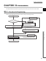
This chapter describes the procedures before starting the operation.
Start
Module connecting
Connect the D/A converter module in any desired
configuration.
(
Page 31, Section 5.1 )
Wiring
Connects external devices to the D/A converter
module.
(
Page 37, Section 6.4 )
4
NO
Use user range settings?
YES
Offset/gain setting
To use user range settings, set the offset/gain
values.
(
Page 42, Section 7.5 )
Programming and debugging
Creates and checks a program.
29
Memo
30
CHAPTER 5 SYSTEM CONFIGURATION
CHAPTER 5
SYSTEM CONFIGURATION
This chapter describes the overall configuration, number of connectable modules, and compatible software version of
the D/A converter module.
5.1
Overall System Configuration
The following shows a system configuration example for using the D/A converter module.
(1) When connected to a CPU module
5
Display unit
(optional)
Power supply module
CPU module
D/A converter module
I/O module
or intelligent
function module
END cover
5.1 Overall System Configuration
(2) When connected to a head module
Power supply module
Head module
D/A converter module
I/O module or
intelligent function
module
END cover
31
5.2
Applicable System
(1) Number of connectable modules
For the number of connectable modules, refer to the following.
MELSEC-L CPU Module User's Manual (Hardware Design, Maintenance and Inspection)
MELSEC-L CC-Link IE Field Network Head Module User's Manual
(2) Compatible software version
For the compatible software versions, refer to the following.
MELSEC-L CPU Module User's Manual (Hardware Design, Maintenance and Inspection)
MELSEC-L CC-Link IE Field Network Head Module User's Manual
5.3
Restrictions When D/A Converter Module is Connected
to Head Module
The following describes the restriction when the D/A converter module is connected to a head module.
• Dedicated instruction cannot be used.
32
CHAPTER 6 INSTALLATION AND WIRING
CHAPTER 6
INSTALLATION AND WIRING
This chapter describes the installation and wiring of the D/A converter module.
6.1
Installation Environment and Installation Position
For precautions for installation environment and installation position, refer to the following.
MELSEC-L CPU Module User's Manual (Hardware Design, Maintenance and Inspection)
MELSEC-L CC-Link IE Field Network Head Module User's Manual
6
6.1 Installation Environment and Installation Position
33
6.2
Terminal Block
(1) Precautions
Tighten the terminal block screws within the following specified torque range.
Screw type
Tightening torque range
Terminal screw (M3 screw)
0.42 to 0.58N • m
Terminal block mounting screw (M3.5 screw)
0.66 to 0.89N • m
The following table shows the applicable solderless terminal installed to the terminal block. For wiring, use the
wire applicable to the following wire and mount with the applicable tightening torque. Use a UL-approved
solderless terminal and tools recommended by the manufacturer of the solderless terminal. The sleeve solderless
terminal cannot be used.
Solderless terminal
Model Name
R1.25-3
Applicable
tightening torque
0.42 to 0.58N • m
Wire
Wire diameter
Type
Material
22 to 18 AWG
Stranded wire
Copper wire
Temperature
rating
75°C or higher
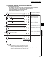
(2) Signal names of the terminal block
The following shows signal names of the terminal block.
Pin number
Signal name
1
2
V+
CH1
3
CH1
CH1 v+
COM CH1
I+
SLD
CH2
CH2 V+
COM CH2
I+
SLD
CH3
CH3 V+
COM CH3
I+
SLD
CH4
CH4 V+
COM CH4
I+
+24V
24G
FG
34
4
I+
SLD
5
6
V+
CH2
7
8
I+
V+
CH3
11
12
COM
I+
SLD
13
14
COM
SLD
9
10
COM
V+
CH4
15
COM
I+
16
+24V
17
24G
18
FG
CHAPTER 6 INSTALLATION AND WIRING
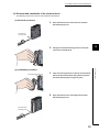
(3) Removal and installation of the terminal block
The following shows how to remove and install the terminal block.
(a) Removal procedure
1.
Open the terminal cover and loosen the terminal
block mounting screw.
Terminal block
mounting screw
2.
Using the terminal block fixing holes as a fulcrum,
6
remove the terminal block.
Terminal block fixing hole
1.
Fully insert the projections on the top of the terminal
block into the terminal block fixing holes and press
the terminal block until it snaps into place.
2.
Open the terminal cover and tighten the terminal
block mounting screw.
Terminal block
mounting screw
35
6.2 Terminal Block
(b) Installation procedure
6.3
Wiring
(1) Wiring to a terminal block
The following shows wirings to a terminal block.
(a) For voltage output
CH1
COM
CH1
V+
CH1
CH1
I+
SLD
CH2
COM
CH2
V+
CH2
CH2
I+
SLD
CH3
COM
CH3
V+
CH3
CH3
I+
SLD
CH4
COM
CH4
V+
CH4
CH4
I+
+24V
24G
FG
(b) For current output
CH1
COM
CH1
V+
CH1
I+
CH1
SLD
CH2
COM
CH2
V+
CH2
I+
CH2
SLD
CH3
COM
CH3
V+
CH3
I+
CH3
SLD
CH4
COM
CH4
V+
CH4
I+
+24V
24G
FG
36
CH4
CHAPTER 6 INSTALLATION AND WIRING
6.4
External Wiring
The following describes the external wiring.
(1) For voltage output
*1
*2
Motor drive
module, etc.
CH1
D/A
conversion
1k
V+
COM
1M
GND
*3
SLD
Motor drive
module, etc.
CH2
1k
V+
COM
1M
GND
SLD
Motor drive
module, etc.
CH3
D/A
conversion
1k
V+
COM
6
1M
GND
*3
SLD
Motor drive
module, etc.
CH4
1k
V+
COM
1M
GND
+24V
DC/DC converter
Filter
DC24V
24G
FG
AG
*1
*2
6.4 External Wiring
(2) For current output
Motor drive
module, etc.
CH1
D/A
conversion
0
I+
COM
600
GND
*3
SLD
Motor drive
module, etc.
CH2
I+
0
COM
600
GND
SLD
Motor drive
module, etc.
CH3
D/A
conversion
0
I+
COM
600
GND
*3
SLD
Motor drive
module, etc.
CH4
0
I+
COM
600
GND
+24V
DC/DC converter
Filter
DC24V
24G
FG
AG
*1
*2
*3
For wire, use the shielded twisted pair cable.
For external wiring, if noise or ripple occurs, connect a capacitor with values between 0.1µF and 0.47µF with voltage
around of 25V between terminal (V+) and COM.
Connect the each channel shielded wire to any one of three shield terminals for the channel. Be sure to ground the FG
terminal.
In addition, ground the FG terminal of the power supply module.
37
CHAPTER 7
VARIOUS SETTINGS
This chapter describes the setting procedures of the D/A converter module.
After writing the contents of new module, switch settings, parameter settings and auto refresh settings into the CPU module,
reset the CPU module, switch STOP → RUN → STOP → RUN, or switch OFF → ON the power supply, to validate the
setting contents.
7.1
Addition of Modules
Add the model name of D/A converter modules to use on the Project.
(1) Addition procedure
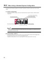
Open the "New Module" dialog box.
Project window
[Intelligent Function Module]
Item
Module Type
Mount Position
Title Setting
38
Right-click
[New Module…]
Description
Module Type
Set "analog module".
Module Name
Select the name of the module to be connected.
Mounted Slot No.
Set the slot No. where the target module is connected.
Specify start X/Y
The start I/O number (hexadecimal) of the target module is set, according to
address
the mounted slot No. Setting any start I/O number is also possible.
Title
Set any title.
CHAPTER 7 VARIOUS SETTINGS
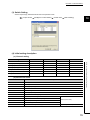
7.2
Switch Setting
Set the operation mode, HOLD/CLEAR function, and the output range used in each CH.
(1) Setting procedure
Open the "Switch Setting" dialog box.
Project window
[Intelligent Function Module]
module name
[Switch Setting]
7
7.2 Switch Setting
Item
Description
Setting value
• 4 to 20mA (default value)
• 0 to 20mA
Output range
Set the output range used in each CH.
Output Range
• 1 to 5V
• 0 to 5V
• -10 to 10V
Setting
• User range setting
HOLD/CLEAR
function
Operation Mode Setting
Set whether to hold or clear the output analog
value in each CH when the CPU module enters
to the STOP status or when an error occurs.
• CLEAR (default value)
• HOLD
Set the operation mode of the D/A converter
• Normal mode (default value)
module.
• Offset/gain setting mode
39
7.3
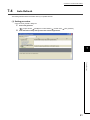
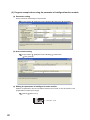
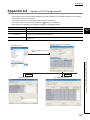
Parameter Setting
Set the parameters of each CH.
(1) Setting procedure
Open the "Parameter" dialog box.
1.
Start "Parameter"
Project window
[Intelligent Function Module]
module name
"Parameter"
Pull-down list type
Text box type
2.
Double-click the item to change the setting, and input the setting value.
• Items to input from the pull-down list
Double-click the item to set, to display the pull-down list. Select the item.
• Items to input from the text box
Double-click the item to set, and input the setting value.
3.
For setting CH2 to CH4, follow the operation of step2.
Item
Basic setting
D/A conversion enable/disable setting
Warning output setting
Warning Output Function
40
0: Enable
1: Disable (default value)
Reference
Page 49,
Section 8.1
0: Enable
1: Disable (default value)
Warning output upper limit value
-32768 to 32767 (default value: 0)
Warning output lower limit value
-32768 to 32767 (default value: 0)
Scaling function
Scaling function
Setting value
Page 59,
Section 8.6
0: Enable
1: Disable (default value)
Scaling upper limit value
-32000 to 32000 (default value: 0)
Scaling lower limit value
-32000 to 32000 (default value: 0)
Page 54,
Section 8.5
CHAPTER 7 VARIOUS SETTINGS
7.4
Auto Refresh
This setting transfers data in the buffer memory to specified devices.
(1) Setting procedure
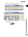
Open the "Auto_Refresh" dialog box.
1.
Start "Auto_Refresh"
Project window
2.
[Intelligent Function Module]
module name
[Auto_Refresh]
Click the item to setup, and input the auto refresh target device.
7
7.4 Auto Refresh
41
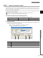
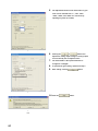
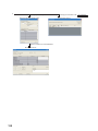
7.5
Offset/Gain Setting
When using the user range setting, configure the offset/gain setting with the following operations.
When using the factory default setting, the offset/gain setting is not necessary.
The offset/gain setting can be configured from the following two types of operations.
• Setting from "Offset/Gain Setting" of GX Works2.
• Setting from a program
7.5.1
Setting from GX Works2 "Offset/Gain Setting"
(1) Setting procedure
Open the "Offset/Gain Setting" dialog box.
[Tool]
[Intelligent Function Module Tool]
1.
[Analog Module]
[Offset/Gain Setting]
Select the module to configure the offset/gain
setting, and click the
button.
↓
2.
↓
42
Click the
button.
CHAPTER 7 VARIOUS SETTINGS
3.
Specify the channel to use the offset/gain setting.
4.
Use the radio button to specify whether to perform
↓
7
the offset setting or gain setting.
(Step 5 and later describes when the offset setting
is specified.)
7.5 Offset/Gain Setting
7.5.1 Setting from GX Works2 "Offset/Gain Setting"
↓
43
5.
The adjustment amount of the offset value or gain
value can be selected from "1", "100", "500",
"1000", "2000", and "3000" or it can be set by
inputting any value (1 to 3000).
↓
6.
Clicking the
or
button fine-
adjusts the analog output voltage or analog output
current value by the set adjusted value.
7.
The offset status in the specified channel is
changed to "Changed".
8.
To perform the gain setting, repeat from step 4.
9.
After setting, click the
button.
↓
10. Click the
↓
End
44
button.
CHAPTER 7 VARIOUS SETTINGS
7.5.2
Setting from a program
(1) Setting procedure
The following describes the procedures when setting the offset/gain from a program.
Start
1
Turns on Channel change request (YB).
Switches to the Offset/gain setting mode.*1
Checks that Channel change completed flag
(XB) is on.
Checks that the module is in Offset/gain
setting mode (the RUN LED is flashing).
Turns off Channel change request (YB).
2
Specifies the offset target channel in
Offset/gain setting mode Offset specification
(Un\G22).
Only one channel can be set at a time. Set "0"
in Offset/gain setting mode Gain specification
(Un\G23).
Sets a value in Offset/gain adjustment value
specification (Un\G24).
Turns on Set value change request (YC).
7
No
Turns on Channel change request (YB).
Turns off the Set value change request (YC)
when Set value change completed flag (XC)
turns on by the analog output value changes.
Checks that Channel change completed flag
(XB) is on.
No
Is the analog output value satisfied?
Turns off Channel change request (YB).
7.5 Offset/Gain Setting
7.5.2 Setting from a program
Yes
Sets a value in Offset/gain adjustment value
specification (Un\G24).
Adjust other channels?
Yes
No
2
Turns on User range writing request (YA).
Turns on Set value change request (YC).
Turns off Set value change request (YC)
when Set value change completed flag (XC)
turns on by the analog output value changes.
No
Is the analog output value satisfied?
Checks that Offset/gain setting mode flag
(XA) has turned off, and then turn off User
range writing request (YA).
Is the "ERR." LED on?
Yes
No
Yes
1
Specifies the offset target channel in
Offset/gain setting mode Gain specification
(Un\G23).
Only one channel can be set at a time. Set "0"
in Offset/gain setting mode Offset
specification (Un\G22).
*1
Switches to the normal mode.*1
End
The following shows the procedure for switching the mode (normal mode offset/gain setting mode normal mode).
Dedicated instruction (G(P).OFFGAN) (
Page 116, Appendix 5.2)
• Changing for Mode switching setting (Un\G158, Un\G159) and OFF → ON → OFF of Operating condition setting
request (Y9) (
Page 110, Appendix 2(14))
• Intelligent function module switch setting (
Page 39, Section 7.2 (1))
45
● Configure the offset/gain setting in accordance with the actual use situation.
● Offset and gain values are recorded in the flash memory in the D/A converter module by turning OFF → ON → OFF User
range writing request (YA). Once recorded, the values are not deleted even after turning the power off.
When the values are written 26 times in succession, an error occurs and the error code is stored in Latest error code
(Un\G19) to prevent an improper write to flash memory.
● Configure the offset/gain setting in the range satisfying the following condition.
When the setting value out of the range is configured, the resolution and accuracy of the module may not fall within the
range shown in the following performance specifications.
• I/O conversion characteristic of D/A conversion (
Page 112, Appendix 3)
● Configure the offset/gain setting for each channel.
When configuring the setting for offset and gain channels at the same time, an error occurs and ERR. LED turns on.
● When error occurs even in one channel, offset/gain value is not written to the module.
Check the value in Latest error code (Un\G19) and perform the following procedures to reconfigure the offset/gain setting
from the beginning.
• Error code list (
Page 93, Section 11.4)
● When the mode is switched from the offset/gain setting mode to the normal mode by the setting of the dedicated
instruction (G(P).OFFGAN) or Mode switching setting (Un\G158, Un\G159), Module READY (X0) turns from OFF to ON.
Note the initial setting process is executed at the switching of the mode if the sequence program executes the initial
setting at Module READY (X0) ON.
● To validate the intelligent function module switch setting after writing the setting to the CPU module, reset the CPU
module or turn the power supply from OFF to ON.
(2) Program example
(a) Device
Ex. I/O number of D/A converter module is X/Y30 to 3F (when L26CPU-BT is used)
The following shows the devices used in the program example.
Device
Function
M0
Channel selection
M2
Gain setting
M3
Channel change command
M4
Offset/gain setting value channel change command
M5
Mode switching
M6
Analog output value adjustment command
M7
Command to write offset/gain setting values to the module
M8
Adjustment amount setting
M50
Signal for checking the offset/gain setting mode
M51
Signal for checking the normal mode
D0
Channel-specified storage device
D1
Adjustment amount setting storage device
D2
Storage device for the setting value of the dedicated instruction (G(P).OFFGAN)
M100
Module READY checking flag
For configuring the same I/O assignment as the system above, when using L02CPU, set the I/O assignment of the D/A
converter module within X/Y30 to 3F.
46
CHAPTER 7 VARIOUS SETTINGS
(b) Switching the mode by the dedicated instruction (G.OFFGAN)
This program performs the followings:
• first, switches the mode to the offset/gain setting mode by the dedicated instruction (G.OFFGAN),
• second, switches the channels for which the offset/gain settings are configured,
• third, writes the offset/gain value to the D/A converter module,
• finally, switches the mode back to the normal mode.
Switches to the Offset/gain setting mode
Stores the setting data of the dedicated
instruction (G.OFFGAN) in D2.
Dedicated instruction (G.OFFGAN).
Switches to the Offset/gain setting channel
Sets the offset/gain setting mode.
Stores the channel number to D0.
Specifies the offset target channel.
Sets the buffer memory address 23 to 0.
Sets the buffer memory address 22 to 0.
Specifies the gain target channel.
Turns on Channel change request (YB).
7
Turns off Channel change request (YB).
Sets the changed value in one time for the range between -3000 and 3000 when adjusting
Sets the adjustment of offset value to D1.
Sets the buffer memory address24 to D1.
Adjusts the analog output value
Turns off Set value change request (YC).
Registers the Offset/gain setting result to the modules
Turns on User range writing request (YA).
Turns off User range writing request (YA).
Switches to the normal mode
Stores the setting data of the dedicated
instruction (G.OFFGAN) in D2.
Dedicated instruction (G.OFFGAN)
Processing in normal mode
The program in the dot-line box is common with the following three programs.
• Switching the mode by the dedicated instruction (G(P).OFFGAN)
• Switching the mode by Mode switching setting (U3\G158, U3\G159) and Operating condition setting request
(Y39)
• Switching the mode by the intelligent function module switch setting
47
7.5 Offset/Gain Setting
7.5.2 Setting from a program
Turns on Set value change request (YC).
(c) Switching the mode by Mode switching setting (Un\G158, Un\G159) and Operating
condition setting request (Y9)
Normal mode initial setting
D/A conversion enable/disable program
Setting programs for other initial setting items
Turns on Operating condition setting
request (Y39).
Switches to the Offset/gain setting mode
Sets 4144H to Mode switching setting
(U3\G158).
Sets 964H to Mode switching setting
(U3\G159).
Turns on Operating condition setting
request (Y39).
Common program
Switches to the normal mode
Sets 964H to Mode switching setting
(U3\G158).
Sets 4144H to Mode switching setting
(U3\G159).
Turns off Operating condition setting
request (Y39).
One second timer
(d) Switching the mode by the intelligent function module switch setting
The program other than the common program is not required.
48
CHAPTER 8 FUNCTIONS
CHAPTER 8
FUNCTIONS
This chapter describes the details on functions that can be used in the D/A converter module and the setting
procedures.
For details on I/O signals and buffer memory, refer to the following.
• Detail of I/O signals (
Page 98, Appendix 1)
• Details of buffer memory addresses (
8.1
Page 104, Appendix 2)
D/A Conversion Enable/Disable Function
This function sets whether to enable or disable the analog value output for each channel.
Disabling the D/A conversion for unused channels reduces the conversion cycles.
(1) Setting procedure
Set "D/A conversion enable/disable setting" to "0: Enable".
Project window
[Intelligent Function Module]
module name
[Parameter]
8
8.1 D/A Conversion Enable/Disable Function
8.2
D/A Output Enable/Disable Function
This function sets whether to output the D/A conversion value or the offset value, for each channel.
The conversion speed is constant, regardless of the output enable/disable status.
(1) Setting procedure
Configure the setting with CH Output enable/disable flag (Y1 to Y4)
CH Output enable/disable flag (Y1 to Y4)
Analog output
Enable (ON)
D/A conversion value is output.
Disable (OFF)
Offset value is output.
49
8.3
Analog Output HOLD/CLEAR Function
This function sets whether to hold the output analog value (HOLD) or clear the output analog value (CLEAR),
according to the CPU module operating status (RUN, STOP or stop error).
(1) Combination of analog output statuses
The analog output status changes as shown in the following table, depending on the combination of settings for
D/A conversion enable/disable setting (Un\G0) and CH Output enable/disable flag (Y1 to Y4).
D/A conversion enable/disable
Enable
setting (Un\G0)
Execution
CH Output enable/disable flag
status
(Y1 to Y4)
Analog output HOLD/CLEAR
function setting
Analog output status when CPU module is in RUN status
Enable
HOLD
Disable
Disable
CLEAR
Analog value converted from digital
value with D/A conversion is output.
Enable or
disable
HOLD
HOLD
or CLEAR
or CLEAR
Offset value
0V/0mA
Analog output status when CPU module is in STOP status
Hold
Offset value
Offset value*2
0V/0mA
Analog output status when CPU module is in stop error
Hold
Offset value
Offset value
0V/0mA
0V/0mA
0V/0mA
0V/0mA
0V/0mA
1
Analog output status when a watchdog timer error* occurs
*1
*2
Occurs when the program operation is not completed within the estimated time due to such as a hardware trouble in the
D/A converter module. When a watchdog timer error occurs, Module READY (X0) turns OFF and the RUN LED on the
D/A converter module turns off.
The following operation is performed when the CPU module is in STOP status, D/A conversion enable/disable setting
(Un\G0) is set to D/A conversion enabled (0) and Operating condition setting request (Y9) is turned to OFF → ON →
OFF.
Output enable/disable flag OFF: 0 V/0 mA output
Output enable/disable flag OFF → ON: offset value output
(2) Setting procedure
Configure the setting from "HOLD/CLEAR function".
Project window
50
[Intelligent Function Module]
module name
[Switch Setting]
CHAPTER 8 FUNCTIONS
The following describes the conditions for using the analog output HOLD/CLEAR function with a head module.
• Enable the station-based block data assurance of the cyclic data on the send side.
• When a link error occurs, configure the setting to hold the D/A conversion output through "I/O assignment setting
error output mode" *1. The HOLD/CLEAR setting configured from the Switch Setting of the intelligent function
module switch will be invalid.
This setting is enabled for each module. Setting by each channel are not available.
Therefore, set the HOLD/CLEAR function to the same setting for all channels in order to match the output status when a
CPU module occurs a stop error or actually stopped and when a link error occurs.
Project window
[Parameter]
[PLC Parameter]
[I/O Assignment]
button
Operating status
Holds the analog output
(Outputs offset value)
HOLD/CLEAR setting (All channels
should be the same settings)
Hold
HOLD
Clear
CLEAR
For the block guarantee of cyclic data per station, refer to the following manual.
MELSEC-Q CC-Link IE Field Network Master/Local Module User's Manual
*1
8
8.3 Analog Output HOLD/CLEAR Function
Clears the analog output
Error time output
mode *1
When the error time output mode is enabled
• Data link stopped due to a network error
• Data link is stopped by CC-Link IE Field diagnostics using GX Works2
51
8.4
Analog Output Test when CPU Module is in STOP Status
Analog output test can be performed when CPU module is in STOP status.
When the following settings are configured, the settings are enabled even during the analog output test.
• Alarm output function (
• Scaling Function (
Page 59, Section 8.6)
Page 54, Section 8.5)
When a digital value out of the range is written to each channel, a check code is stored in CH Set value check code
(Un\G11 to Un\G14).
(1) Setting procedure
For analog output test, configure the following settings in the device test of GX Works2.
1.
Set D/A conversion enable/disable setting (Un\G0) to "enable" for the channel where the analog
output test is to be performed.
2.
3.
Turn OFF → ON → OFF Operating condition setting request (Y9).
Turn OFF → ON Output enable/disable flag (Y1 to Y4) for the channel where the analog output test
is to be performed.
4.
Set the digital value equivalent to the analog value to be output to CH Digital value (Un\G1 to
Un\G4) in buffer memory.
D/A conversion enable/disable
Setting
setting (Un\G0)
combination
CH Output enable/disable flag
Enable
(Y1 to Y4)
Analog output test
*1
Disable
Enable
Disable
Allowed
Not allowed
Enable
Disable
Not allowed*1
When performing the analog output test, set D/A conversion enable/disable setting (Un\G0) to "enable" beforehand.
(2) Operation timing
By forcibly turning CH Output enable/disable flag (Y1 to Y4) OFF → ON when the CPU module is in STOP
status, analog output value is changed from offset value to D/A-converted analog value.
The following shows the relation between CH1 Output enable/disable flag (Y1) and analog output value when the
CPU module is in STOP status.
D/A conversion is output even when CPU STOP is operated.
CPU module
status
RUN
STOP
RUN
ON*3
CH1 Output
enable/disable
flag (Y1)
OFF*2
Analog output
Analog output value
converted from digital value
value status
*2
*3
52
Offset value
ON
OFF
Analog output value
converted from digital value
Offset value
Analog output value
converted from digital value
CH1 Output enable/disable flag (Y1) turns OFF with CPU STOP.
By forcibly turning the CH1 Output enable/disable flag (Y1) OFF → ON, analog output value is changed from offset value
to D/A-converted analog value.
CHAPTER 8 FUNCTIONS
Analog output tests can be performed if a head module is connected even when the CPU module is stopped due to an error.
8
8.4 Analog Output Test when CPU Module is in STOP Status
53
8.5
Scaling Function
This function converts the input digital value to the scaled value of -20000 to 20000 (or 0 to 20000) using the specified
scaling upper and lower limit values, and outputs the corresponding analog value.
(1) Concept of scaling setting
The setting for scaling lower and upper limit values differs depending on either the factory default setting or the
user range setting is used for analog output range.
(a) When the factory default setting is used for analog output range
When using the factory default range, set a value corresponding to the upper limit value of the analog output
value of the factory default range for the scaling upper limit value. Also, set a value corresponding to the lower
limit value of the analog output of the factory default range for the scaling lower limit value.
(b) When the user range setting is used for analog output range
When using the user range, set a value corresponding to the analog output gain value for the scaling upper
limit value. Also, set a value corresponding to the analog output offset value for the scaling lower limit value.
(2) Calculating the scaling value
Values converted using the following formulas are used for D/A conversion.
(Values lower than the decimal point are rounded down in scale conversion.)
(a) When the factory default setting is used for output range
• Voltage: 1 to 5 V, 0 to 5 V
Current: 4 to 20 mA, 0 to 20 mA
Digital value used for D/A conversion =
20000
(DX - SL)
SH - SL
• When the voltage is -10 to 10 V
Digital value used for D/A conversion =
40000
(DX - SL) - 20000
SH - SL
(b) When the user range setting is used for output range
Digital value used for D/A conversion =
20000
(DX - SL)
SH - SL
Item
Description
Dx
digital value
DMax
digital maximum value of the used output range
DMin
digital minimum value of the used output range
SH
scaling upper limit value
SL
Scaling lower limit value
Even if the input range of digital value is increased, the resolution does not become higher than that of when the scaling
function is not used.
54
CHAPTER 8 FUNCTIONS
(3) Setting procedure
1.
Set "D/A conversion enable/disable setting" to "0: Enable".
Project window
[Intelligent Function Module]
module name
[Parameter]
2.
Set "Scaling function" to "0: Enable".
3.
Set values for "Scaling upper limit value" and "Scaling lower limit value".
Item
Scaling upper limit value
Scaling lower limit value
8
Setting range
-32000 to 32000
8.5 Scaling Function
● Your scaling settings must meet the following condition:
Scaling upper limit value > Scaling lower limit value
55
(4) Scaling setting example
Ex. 1. When setting the "Scaling upper limit value" to "16000" and the "Scaling lower limit value" to "4000" for a
channel with output range of 0V to 5V:
The following shows the digital values before and after scaling.
Analog output voltage (V)
5V
0V
Digital value
20000 20479
0
Scaling lower limit
value 4000
56
Scaling upper limit
value 16000
Analog output voltage (V)
Digital value
Digital value after scaling
0
4000
0
1
6400
4000
2
8800
8000
3
11200
12000
4
13600
16000
5
16000
20000
CHAPTER 8 FUNCTIONS
Ex. 2. When setting the "Scaling upper limit value" to "16000" and the "Scaling lower limit value" to "4000" for a
channel with output range of -10V to 10V:
The following shows the digital values before and after scaling.
Analog output voltage (V)
10V
-10V
-20480 -20000
Scaling lower limit
value 4000
8
Digital value
20000 20479
0
Scaling upper limit
value 16000
10000
Digital value
Digital value after scaling
-10
4000
-20000
-5
7000
-10000
0
10000
0
5
13000
10000
10
16000
20000
8.5 Scaling Function
Analog output voltage (V)
57
Ex. 3: When setting the "Scaling upper limit value" to "16000" and the "Scaling lower limit value" to "4000" for a
channel with output range of -8V to 8V:
The following shows the digital values before and after scaling.
Analog output voltage (V)
8V
0V
-8V
-20480 -20000
-8000
20000 20479 Digital value
0
Scaling lower limit
value 4000
Scaling upper limit
value 16000
Analog output voltage (V)
Digital Value
Digital value after scaling
-8
-8000
-20000
-4
-2000
-10000
0
4000
0
4
10000
10000
8
16000
20000
● When using the scaling function, the digital value before scaling can be set to a value out of the range of scaling upper
and lower limit values (dotted line area in the I/O characteristics). However, use the scaling function within the range of
analog output practical range (solid line area in the I/O characteristics). If the value exceeds the analog output practical
range, the resolution and accuracy may not fall within the range of performance specifications.
● The default digital value "0" may not be appropriate, depending on the scaling function setting.
Especially in the examples 1 and 2, the out-of-range digital value error (error code: 60) occurs if the output enable/
disable flag is turned on with the digital value "0".
Therefore, be sure to set an appropriate digital value, within the scaling range, before turning on the output enable/
disable flag.
The following shows the error codes that occur.
60
Fixed
Error channel number
● When using the user range, note that the scaling lower limit value is equal to the offset value.
58
CHAPTER 8 FUNCTIONS
8.6
Alarm Output Function
This function outputs an alarm when the digital value is out of the preset range.
Digital value
Digital value
Analog output value
Warning output upper limit value
20000
Warning output lower limit value
-2000
CH1 Warning output flag
(upper limit value) (Un\G48.b0)
OFF
CH1 Warning output flag
(lower limit value) (Un\G48.b1)
OFF
Warning output signal (XE)
OFF
Warning output clear request (YE)
OFF
ON
OFF
ON
ON
8
OFF ON
ON
OFF
When the digital value moves above the alarm output upper limit value, or below the alarm output lower limit
value, alarm notifications are made by Warning output flag (Un\G48), Warning output signal (XE) and the ALM
LED turning ON.
In addition, alarm code 15
is stored in Latest error code (Un\G19).
The alarm code that is stored is shown below:
15
Fixed
Warning channel number
1: Lower limit
0: Upper limit
(2) Operation of alarm output function
When the digital value moves above the alarm output upper limit value, or below the alarm output lower limit
value, alarm notifications are made, and the analog output value becomes any of the following.
• When the digital value exceeds the alarm output upper limit value: An analog value converted from the
digital value of alarm output upper limit value is output.
• When the digital value is less than the alarm output lower limit value: An analog value converted from the
digital value of alarm output lower limit value is output.
After an alarm has occurred, the analog output value returns to the normal value by changing the digital value to
a value within the setting range. However, Warning output flag (Un\G48) and Warning output signal (XE) are not
cleared. (ALM LED keeps ON.)
59
8.6 Alarm Output Function
(1) Alarm output notification
(3) Clearing the Warning output
The alarm output can be cleared in the following two procedures:
• Turning OFF → ON → OFF Warning output clear request (YE)
• Turning OFF → ON → OFF Operating condition setting request (Y9)
Clearing the alarm output puts the D/A converter module into the following status.
• Warning output flag (Un\G48) is cleared.
• Warning output signal (XE) is turned to OFF.
• ALM LED is turned off.
• Warning code: 15
stored in Latest error code (Un\G19) is cleared.
(4) If the scaling function is enabled
If Scaling enable/disable setting (Un\G53) is set to "Enable", the digital value converted to the scaling range
becomes a subject for alarm detection.
When setting CH1 Warning output upper limit value (Un\G86) to CH4 Warning output lower limit value (Un\G93),
make sure to specify values that reflect the scaling range.
(5) Setting procedure
1.
Set "D/A conversion enable/disable setting" to "0: Enable".
Project window
[Intelligent Function Module]
[Parameter]
2.
Set "Warning output function" to "0: Enable".
3.
Set a value for "Warning output upper limit value" and "Warning output lower limit value".
Item
Warning output upper limit value
Warning output lower limit value
60
module name
Setting range
-32768 to 32767
CHAPTER 8 FUNCTIONS
8.7
Error Log Function
This function stores a history of errors and alarms that occurred in the D/A converter module to the buffer memory
(Un\G1810 to Un\G1969).
A maximum of 16 errors and alarms can be stored.
(1) Process of the error log function
The error code and the time of error occurrence are stored in the buffer memory address, starting from error
history No.1 (start address Un\G1810) and sequentially thereafter.
(2) Checking error history
You can check the start address of the latest stored error at Latest error code address (Un\G1800)
Ex. 1. When the third error occurs:
The third error is stored in error history No.3, and the value "1830" (start address of error history No.3) is stored to
Latest error code address (Un\G1800).
Latest error code address
(Un\G1800)
The start address of the error history
where the latest error is stored is stored.
Details of error history
Address
1810
An error history consists of the following
data.
First two digits Last two digits
of the year
of the year
1st error
Month
Hour
Second
Error history No.2
Day
Minute
Error
occurrence
time
8.7 Error Log Function
1820
8
Error code
Error history No.1
Day of the week
2nd error
New
1830
Error history No.3
3rd error
(Empty)
1960
Error history No.16
(Empty)
61
Ex. 2. When the 17th error occurs:
The 17th error is stored in error history no.1, and the value "1810" (start address of error history No.1) is stored to
Latest error code address (Un\G1800).
Latest error code address
(Un\G1800)
Address
1810
New
Error history No.1
1st error
1820
Error history No.2
17th error
The 17th error is stored in Error history
No.1 and the 1st error history will be erased.
2nd error
1830
Error history No.3
3rd error
1960
Error history No.16
16th error
● The same process for errors is used when an alarm occurs.
● Once the error history storage area becomes full, subsequent errors will overwrite the previous errors, starting from error
history No.1, and continues sequentially thereafter (Un\G1810 to G1819). (The overwritten history is deleted.)
● The stored error history is cleared when power supply is turned OFF, or when the CPU module is reset.
62
CHAPTER 8 FUNCTIONS
8.8
Module Error Collection Function
This function collects the errors and alarms occurred in D/A converter module into the CPU module or the head
module. By holding the module errors in a memory that can hold data in the event of power failure, the errors can be
held even after powering off or resetting the CPU module or the head module.
Error history (CPU module including built-in I/O and built-in
CC-Link) and error log (intelligent function module) are
displayed on one screen.
Errors that occurred in the entire system can be
monitored in reverse chronological order.
Module A
CPU
19:33 Error C1 occurred!
Module B
19:29 Error A1 occurred!
19:36 Error A2 occurred!
19:34 Error B1 occurred!
Programming tool
Error history display
Time Module in error
19:29
19:33
19:34
19:36
Module A
CPU
Module B
Module A
Error code
Error A1
Error C1
Error B1
Error A2
Error history
(CPU module)
19:33 Error C1
Module error log
Time
Module in error
Error code
19:29
19:34
19:36
Module A
Module B
Module A
Error A1
Error B1
Error A2
[Example of screen display]
8
8.8 Module Error Collection Function
For details on the module error collection, refer to the following.
MELSEC-L CPU Module User's Manual (Function Explanation, Program Fundamentals)
MELSEC-L CC-Link IE Field Network Head Module User's Manual
63
8.9
Error Clear Function
When an error occurs, you can clear the error from the system monitor.
By clicking the
button in the system monitor, the latest error code stored in Latest error code (Un\G19)
is cleared and the ERR. LED is also turned off. The operation is the same as Error clear request (YF) as well as
executing error clear from the display unit.
However, error history cannot be cleared.
For instructions on error clear request and executing error clear from the display unit, refer to the following.
• Error clear request (YF) (
Page 98, Appendix 1)
• Checking/Clearing an Error (
[Diagnostics]
64
Page 75, Section 9.4)
[System Monitor…]
error module
CHAPTER 8 FUNCTIONS
8.10
Saving and Restoring Offset/Gain Values
The D/A converter module can save and restore the offset/gain values in the user range setting.
When replacing a module in case of failure, this function enables to pass the offset/gain value from a module to be
changed (disconnected) to the newly-connected CPU module.
If multiple D/A converter modules are installed in the same system, this function enables to apply the offset/gain value
set to one module to the other modules.
However, if you save and restore the offset/gain values, the accuracy after the restoration decreases by approximately
three times compared to that before the restoration.
Reconfigure the offset/gain as necessary.
(1) Procedure for saving and restoring offset/gain values
(a) To restore offset/gain values onto a new replacement module:
1.
Save the offset/gain values.
8
↓
Replace the D/A converter module.
3.
Restore the offset/gain values.
8.10 Saving and Restoring Offset/Gain Values
2.
↓
65
(b) To apply the offset/gain values of one module to the other modules in the same
system:
Ex. Here, the offset/gain setting of module No.1 is applied to modules No.2 to No.4.
1.
Save the offset/gain values of module No.1.
2.
Apply the offset/gain values to modules No.2 to No.4.
↓
(2) Methods for saving and restoring offset/gain values
There are two methods for saving and restoring offset/gain values.
• Saving and restoring by dedicated instructions
• Saving and restoring by reading from and writing to the buffer memory
(a) Saving and restoring by dedicated instructions
Temporarily save the offset/ gain value in the source D/A converter module into the internal device of CPU
module using G(P).OGLOAD of dedicated instruction. Then, write the data to the restoring target D/A converter
module using G(P).OGSTOR.
You can prevent the saved offset/gain value data from getting deleted, by doing one of the following before
replacing the modules:
• Use latch settings for the internal device of the destination module.
• Save the data onto an SD card
To write data: use SP.FWRITE instruction
To read data: use SP.FREAD instruction
• Store the saved data
For use of dedicated instructions, refer to the following.
• Dedicated Instructions (
Page 115, Appendix 5)
When performing the dedicated instruction G(P).OGSTOR, the D/A conversion is stopped.
Turn OFF → ON → OFF Operating condition setting request (Y9) to restart the D/A conversion.
66
CHAPTER 8 FUNCTIONS
(b) Saving and restoring by reading from and writing to the buffer memory
In the buffer memory, use Pass data classification setting (Un\G200), CH1 Industrial shipment settings offset
value (Un\G202) to CH4 User range settings gain value (Un\G217) and User range writing request (YA) to read
the offset/gain values from the source D/A converter module, then use the buffer memory again to write to the
destination D/A converter module.
The procedure for using the buffer memory is described below.
• To restore offset/gain values onto a new replacement module:
Start
Sets values in Pass data classification setting (Un\G200).
Turns off, then on, and off again Operating condition
setting request (Y9).
For the source D/A converter module
Takes down the values stored in Pass data classification setting
(Un\G200) and CH1 Industrial shipment settings offset value
(Un\G202) to CH4 User range settings gain value (Un\G217).*1
Turns off the power.
8
Replaces the D/A converter module.
Turns on the power.
8.10 Saving and Restoring Offset/Gain Values
Writes the recorded data to Pass data classification setting
(Un\G200) and CH1 Industrial shipment settings offset value
(Un\G202) to CH4 User range settings gain value (Un\G217).*1
Turns off and then on User range writing request (YA).
Checks that Offset/gain setting mode flag (XA) is on.
For the destination D/A converter module
Turns on and then off User range writing request (YA).
Turns off, then on, and off again Operating condition
setting request (Y9).
Checks that the replaced D/A converter module operates
with the restored offset/gain values.
End
*1
When replacing modules, you can prevent the saved offset/gain value data from getting deleted, by doing one of the
following before turning the power off:
• Use latch settings for the internal device of the destination module.
• Save the data onto an SD card.
To write data: use SP.FWRITE instruction
To read data: use SP.FREAD instruction
• Store the saved data.
67
• To apply the offset/gain values of one module to the other modules:
Start
Sets values in Pass data classification setting (Un\G200).
Turns off, then on, and off again Operating condition
setting request (Y9).
For the source D/A converter module
Records the data stored in Pass data classification setting
(Un\G200) and CH1 Industrial shipment settings offset value
(Un\G202) to CH4 User range settings gain value (Un\G217).
Writes the recorded data to Pass data classification setting
(Un\G200) and CH1 Industrial shipment settings offset value
(Un\G202) to CH4 User range settings gain value (Un\G217).
Turns off and then on User range writing request (YA).
Checks that Offset/gain setting mode flag (XA) is on.
For the destination D/A converter module
Turns on and then off User range writing request (YA).
Turns off, then on, and off again Operating condition
]setting request (Y9).
Checks that the replaced D/A converter module operates
with the restored offset/gain values.
End
When the data is written to the following buffer memory address in the source D/A converter module and User range writing
request (YA) is turned from OFF to ON, the D/A conversion is stopped.
• Pass data classification setting (Un\G200)
• CH1 Industrial shipment settings offset value (Un\G202) to CH4 User range settings gain value (Un\G217)
Turn OFF → ON → OFF Operating condition setting request (Y9) to restart the D/A conversion.
68
CHAPTER 8 FUNCTIONS
(3) Range reference tables
Below are reference ranges to be used for saving and restoring offset/gain values.
(a) Reference table for CH1 Industrial shipment settings offset value (Un\G202) to CH4
Industrial shipment settings gain value (Un\G209)
The reference values will vary depending on the Pass data classification setting (Un\G200) (voltage or current).
Address (decimal)
CH1
CH2
CH3
Pass data
Description
CH4
202
204
206
208
203
205
207
209
Reference
classification
value
setting
(hexadecimal)
Industrial shipment settings offset
Voltage
Approx. 8000H
value
Current
Approx. 8000H
Industrial shipment settings gain
Voltage
Approx. F712H
value
Current
Approx. F166H
(b) Reference table for CH1 User range settings offset value (Un\G210) to CH4 User
range settings gain value (Un\G217)
Offset/gain value
Voltage
*1
*2
(hexadecimal)
0V
Approx. 8000H
1V
Approx. 8BE8H
5V
Approx. BB89H
10V
Approx. F712H
0mA
Approx. 8000H
4mA*1
Approx. 96AEH
20mA*2
Approx. F166H
8
8.10 Saving and Restoring Offset/Gain Values
Current
Reference value
This is the value that is stored in user range settings offset value at the time of shipping.
This is the value that is stored in user range settings gain value at the time of shipping.
69
CHAPTER 9
DISPLAY UNIT
This chapter describes the functions of the display unit that can be used in D/A converter module.
For instruction on operating the display unit, or for details on the functions and menu configuration, refer to the
following.
MELSEC-L CPU Module User's Manual (Function Explanation, Program Fundamentals)
9.1
Display Unit
The display unit is an LCD to be attached to the CPU module. By attaching the display unit to the CPU module, you
can check the status of the system and change system settings without the software package. In addition, in the event
a problem occurs, you can identify the cause of the problem by displaying the error information on the display unit.
For details on how to check and clear an error from the display unit, refer to the following.
• Check/clear error (
9.2
Page 75, Section 9.4)
Menu Structure
(1) Organization
The diagram below shows how the "MOD MON/TEST" menu and "MOD SETTINGS" are organized.
CPU MON/TEST
CPU SETTINGS
MOD MON/TEST
SPECIFY I/O No.
BUF MEM MON/TES
MODULE LIST
MOD SETTINGS
SPECIFY I/O No.
MODULE LIST
USER MESSAGE
INIT CHANGE
CH1
D/A CONVERSION
CH2
WARN OUTPUT
CH3
WARN UP LIMIT
CH4
WARN LOW LIMIT
SCALING
OPTIONS
SCALE UP LIMIT
SCALE LOW LIMIT
70
CHAPTER 9 DISPLAY UNIT
9
(2) Screen transitions up to the initial setting change screen
The diagram below shows how the screens transition to the initial setting change screen.
D/A conversion enable and
disable setting screen
Standby screen
Warning output setting screen
Function selection screen
Warning output upper limit screen
Module setting_module
specification screen
Module setting_start I/O No.
specification screen
Warning output lower limit screen
9.2 Menu Structure
INIT CHANGE
Module setting_module
selection screen
Scaling setting screen
Initial setting change screen
Change item selection
menu screen
Parameter-valid drive
confirmation screen
Scaling upper limit screen
Scaling lower limit screen
Channel selection screen
71
9.3
List of Setting Value Change Screens
The following is a list of setting value change screens.
(1) Displayed in English:
Name
Setting item
Screen
Screen display
format
Input regulation
Upper limit
Lower limit
value
value
D/A conversion enable/disable setting
D/A CONVERSION
Selection
⎯
⎯
Warning output setting
WARNING OUTPUT
Selection
⎯
⎯
Warning output upper limit value
WARN UP LIMIT
32767
-32768
Warning output lower limit value
WARN LOW LIMIT
32767
-32768
Scaling enable/disable setting
SCALING
⎯
⎯
Scaling upper limit value
SCALE UP LIMIT
32000
-32000
Scaling lower limit value
SCALE LOW LIMIT
32000
-32000
72
Numeric
value
Numeric
value
Selection
Numeric
value
Numeric
value
CHAPTER 9 DISPLAY UNIT
9
(2) D/A CONVERSION
Select "DISABLE" or "ENABLE" in the "D/A conversion enable/disable conversion" screen.
"D/A conversion enable/disable conversion" screen
1.
Use the
and
buttons to select "DISABLE" or
"ENABLE", and then confirm with the
OK
button.
(3) Warning output setting
Select "DISABLE" or "ENABLE" on the "Warning output setting" screen.
"Warning output setting" screen
1.
Use the
and
buttons to select "DISABLE" or
"ENABLE", and then confirm with the
OK
button. (If
you selected "ENABLE", follow the rest of the
procedure.)
↓
"Warning output upper limit" screen
2.
Move the cursor using the
and
buttons, then
increment or decrement the value at the cursor,
using the
with the
and
OK
buttons, respectively. Confirm
button.
"Warning output lower limit" screen
3.
Move the cursor using the
and
buttons, then
increment or decrement the value at the cursor,
using the
with the
and
OK
buttons, respectively. Confirm
button.
Table of input items
Input item
WARN UP LIMIT
WARN LOW LIMIT
Input range
Input upper limit
Input lower limit
32767
-32768
73
9.3 List of Setting Value Change Screens
↓
(4) SCALING
Select "DISABLE" or "ENABLE" in the "Scaling setting" screen.
"Scaling setting" screen
1.
Use the
and
buttons to select "DISABLE" or
"ENABLE", and then confirm with the
OK
button. (If
you selected "ENABLE", follow the rest of the
procedure.)
↓
"Scaling upper limit" screen
2.
Move the cursor using the
and
buttons, then
increment or decrement the value at the cursor,
using the
with the
and
OK
buttons, respectively. Confirm
button.
↓
"Scaling lower limit" screen
3.
Move the cursor using the
and
buttons, then
increment or decrement the value at the cursor,
using the
with the
and
OK
buttons, respectively. Confirm
button.
Table of input items
Input item
SCALE UP LIMIT
SCALE LOW LIMIT
74
Input range
Input upper limit
Input lower limit
32000
-32000
CHAPTER 9 DISPLAY UNIT
9.4
Checking and Clearing Errors
9
You can check the errors that occurred in the D/A converter module, from the display unit. In addition, you can also
clear an error during its occurrence.
(1) Checking errors
You can check the error that occurred in the D/A converter module, by specifying Latest error code (Un\G19) from
"buffer memory monitor/test".
Ex. When an error occurs in the D/A converter module with a start I/O number of 1
"Buffer memory monitor/test" screen
1.
Press the
2.
Use the
OK
button.
↓
"Buffer memory address input format selection" screen
and
buttons to select "DEC" for the
input format of the buffer memory address, and
then confirm with the
OK
button.
↓
"Buffer memory address setting" screen
3.
Move the cursor using the
and
buttons, then
using the
with the
and
OK
buttons, respectively. Confirm
button.
↓
"Buffer memory monitor" screen
4.
You can check the error that occurred, in the "Buffer
memory monitor" screen.
75
9.4 Checking and Clearing Errors
increment or decrement the value at the cursor,
(2) Clearing errors
You can clear an error by eliminating the cause of the error, and turning Error clear request (YF) OFF → ON →
OFF from "Device Monitor/Test".
Ex. When an error occurs in the D/A converter module with a start I/O number of 1
"CPU monitor/test" screen
1.
Use the
and
buttons to select "DEV MON/TES",
and then confirm with the
OK
button.
↓
"Device monitor" screen
2.
Set the device to Y and press the
3.
Use the
OK
button.
↓
"Device test" screen
and
buttons to set the device to Y1F,
and then confirm with the
OK
button.
↓
4.
Use the
the
OK
setting.
76
and
buttons to switch ON/OFF. Press
button to set the value at the device test
CHAPTER 10 PROGRAMMING
CHAPTER 10 PROGRAMMING
10
This chapter describes the procedure for programming and the basic program of the D/A converter module.
10.1
Procedure for Programming
Create a program executed by D/A converter module according to the following procedure.
Start
(1) Initial setting program
Use the configuration
function?
YES
NO
Performs initial setting by using a program.
Page 78, Section 10.2 )
(
Initial setting
D/A conversion enable/disable program
Scaling function program *1
Alarm output function program *1
Switch setting, parameter setting, and auto refresh setting
(
Page 78, Section 10.2 )
*1 A program that is created according to the
function to be used
Program to write a digital value and a scaling value,
and program to read a warning output flag
10.1 Procedure for Programming
(2) Auxiliary program *2
Error reset program
*2 A program that is added according to the
control target (Create a program if needed.)
End
77
10.2
When Using a Standard System Configuration
The following shows program examples for the system configuration and usage conditions of the D/A converter
module.
(1) System configuration
The following shows an example of the system configuration when using the module in a standard system
configuration.
D/A converter module (L60DA4)
Input module (LX40C6)
CPU module (L26CPU-BT)
Power supply module (L61P)
Output module (LY42NT1P)
X/Y00 X/Y10 X/Y30 X/Y40 X/Y50
to
to
to
to
to
X/Y0F X/Y2F X/Y3F X/Y4F X/Y8F
END cover (L6EC)
For configuring the same I/O assignment as the system above, when using the L02CPU, set I/O Assignment of the D/A
converter module within X/Y30 to X/YF. Also, set the I/O assignment of the LX40C6 within X/Y40 to X/Y4F, and the same of
the LY42NT1P, within X/Y50 to X/Y8F.
(2) Programming condition
Set CH1 and CH2 of the D/A converter module to D/A conversion enabled, and then write the digital values.
If a digital value write error occurs, an error code is displayed in BCD.
Configure the scaling setting in CH1 only, and configure the warning output function in CH2 only.
78
CHAPTER 10 PROGRAMMING
(3) Switch Setting
Set the output range, HOLD/CLEAR function and operation mode.
Project window
[Intelligent Function Module]
module name
10
[Switch Setting]
(4) Initial setting description
(a) Channel setting
Setting item
CH1
Enable
CH3
CH4
Enable
Disable
Disable
Warning output setting
Disable
Enable
Disable
Disable
Warning output lower limit value
−
3000
−
−
Warning output upper limit value
−
10000
−
−
Scaling enable/disable setting
Enable
Disable
Disable
Disable
Scaling upper limit value
32000
−
−
−
Scaling lower limit value
0
−
−
−
10.2 When Using a Standard System Configuration
D/A conversion enable/disable setting
CH2
(b) Devices for users
Device
D1
Description
CH1 digital value
D2
CH2 digital value
D8
Warning output flag
D10
Error code
D11
CH1 Scaling value
M20 to 27
Warning output flag
M100
Module READY checking flag
X41
Batch output enable signal
X42
Digital value write command input signal
X44
Alarm output reset signal
X45
Error reset signal
Y50 to 5F
Error code notation (BCD 4 digits)
LX40C6 (X40 to X4F)
LY42NT1P (Y50 to Y5F)
79
(5) Program example when using the parameter of intelligent function module
(a) Parameter setting
Set the contents of initial settings in the parameter.
Project window
[Intelligent Function Module]
module name
[Intelligent Function Module]
module name
"Parameter"
(b) Auto refresh setting
Project window
[Auto_Refresh]
(c) Writing the parameter of intelligent function module
Write the set parameter to the CPU module and reset the CPU module, or then off and then on the
programmable controller power supply.
[Online]
[Write to PLC]
or Power OFF
80
ON
CHAPTER 10 PROGRAMMING
(d) Program example
Writes a digital value
CH1 Digital value setting
10
CH2 Digital value setting
Sets the analog output enable
CH1 Output enable/disable flag
CH2 Output enable/disable flag
Reads the warning output flag
Checks the CH2 warning output.
Warning output processing (upper limit)
CH2 Warning output processing
(upper limit)
Warning output processing (lower limit) CH2 Warning output processing
(lower limit)
Turns on Warning output clear.
Turns off Warning output clear.
Error code display and reset processing
Outputs the error code in BCD.
Error clear request
10.2 When Using a Standard System Configuration
81
(6) Program example when not using the parameter of intelligent function module
Initial setting
D/A conversion enable
Scaling setting
Warning output setting
CH1 Scaling lower limit value
CH1 Scaling upper limit value
CH2 Warning output upper limit value
CH2 Warning output lower limit value
Turns on Operating condition setting
Turns off Operating condition setting
Writes a digital value
CH1 Digital value setting
CH2 Digital value setting
Sets the analog output enable
CH1 Output enable/disable flag
CH2 Output enable/disable flag
Reads the warning output flag
Checks the CH2 warning output.
CH2 Warning output processing
Warning output processing (upper limit) (upper limit)
Warning output processing (lower limit)
CH2 Warning output processing
(lower limit)
Turns on Warning output clear.
Turns off Warning output clear.
Error code display and reset processing
Outputs the error code in BCD.
Error clear request
82
CHAPTER 10 PROGRAMMING
10.3
When D/A Converter Module is Connected to Head
Module
10
This section describes system configuration of the D/A converter module and a program example of operation
condition.
(1) System configuration
Power supply module (Q62P)
Power supply module (L61P)
CPU module (Q10UDHCPU)
Head module (LJ72GF15-T2)
Master/local module (QJ71GF11-T2)
D/A converter module (L60DA4)
Input module (QX10)
Input module (LX40C6)
Output module (QY10)
Output module (LY10R2)
END cover (L6EC)
X/Y00
to
X/Y1F
X/Y20
to
X/Y2F
Masster station (Station No.0)
X/Y30
to
X/Y3F
X/Y1000 X/Y1010 X/Y1020
to
to
to
X/Y100F X/Y101F X/Y102F
Intelligent device station (Station No.1)
Ethernet cable (1000BASE-T)
Network No.1
This section describes the example of outputting analog values by setting CH1 and CH2 of the D/A converter
module to D/A conversion enabled.
When a write error of digital value occurs, the error code is displayed in BCD.
Scaling setting is configured only for CH1 and warning output function only for CH2.
(3) Description of initial setting
Setting items
D/A conversion enable/disable setting
CH1
Enabled
CH2
Enabled
CH3
Disabled
CH4
Disabled
Warning output function
Disabled
Enabled
Disabled
Disabled
Warning output upper limit value
−
10000
−
−
Warning output lower limit value
−
3000
−
−
Scaling enable/disable setting
Enabled
Disabled
Disabled
Disabled
Scaling upper limit value
32000
−
−
−
Scaling lower limit value
0
−
−
−
83
10.3 When D/A Converter Module is Connected to Head Module
(2) Programming conditions
(4) Devices used by a user
Device
Description
W1
CH1 Digital value
W2
CH2 Digital value
W1008
Warning output flag
W1010
Latest error code
M20 to M27
Warning output flag
X21
Batch output enable signal
X22
Digital value write command input signal
X24
Warning output reset signal
X45
Error reset signal
Y30 to Y3F
Error code display (BCD 4 digits)
SB49
Data link status (own station)
QX10 (X20 to X2F)
QY10 (Y30 to Y3F)
SWB0.0
Data link status (each station) (station number 1)
N0
Nesting (station number 1)
M0
Flag for meeting the communication condition (station number 1)
(5) Setting on master station
1.
Create a project on GX Works2.
Select "QCPU (Q mode)" for "PLC Series" and select "Q10UDH" for "PLC Type."
2.
Display the network parameter setting screen and configure the setting as follows.
Project window
[Parameter]
[Ethernet/CC IE/MELSECNET]
84
[Network Parameter]
CHAPTER 10 PROGRAMMING
3.
Display the Network Configuration Setting screen and configure the setting as follows.
Project window
[Parameter]
[Network Parameter]
[Ethernet/CC IE/MELSECNET]
button
10
4.
Display the Refresh Parameter setting screen and configure the setting as follows.
Project window
[Parameter]
[Network Parameter]
[Ethernet/CC IE/MELSECNET]
Write the set parameter to the CPU module of the master station and reset the CPU module, or turn
off and then on the programmable controller power supply.
[Online]
[Write to PLC]
or Power OFF
ON
85
10.3 When D/A Converter Module is Connected to Head Module
5.
button
(6) Setting on intelligent device station
1.
Create a project on GX Works2.
Select "LCPU" for "PLC Series" and select "LJ72GF15-T2" for "PLC Type."
[Project]
2.
[New Project]
Display the PLC Parameter setting screen and configure the setting as follows.
Project window
86
[Parameter]
[PLC Parameter]
"Communication Head Setting"
CHAPTER 10 PROGRAMMING
3.
Add the D/A converter module (L60DA4) to the GX Works2 project.
Project window
[Intelligent Function Module]
Right-click
[New Module]
10
4.
Display the Switch Setting screen for the D/A converter module (L60DA4) and configure the
setting as follows.
Project window
[Intelligent Function Module]
[L60DA4]
[Switch Setting]
10.3 When D/A Converter Module is Connected to Head Module
87
5.
Display the initial setting screen for the D/A converter module (L60DA4) and configure the setting
as follows.
Project window
6.
[Intelligent Function Module]
[L60DA4]
[Parameter]
Display the Auto Refresh setting screen for the D/A converter module (L60D/A4) and configure the
setting as follows.
Project window
[Intelligent Function Module]
[L60AD4]
[Auto_Refresh]
7.
Write the set parameter to the head module and reset the head module, or turn off and then on the
programmable controller power supply.
[Online]
[Write to PLC]
or Power OFF
88
ON
CHAPTER 10 PROGRAMMING
(7) Program example
The following shows a program example. The program is written to the CPU module of the master station.
10
Checking the data link status of station No.1 (head module)
Writing a digital value
CH1 Digital value setting
CH2 Digital value setting
Enabling analog output
CH1 Output enable/disable flag
CH2 Output enable/disable flag
Reading the warning output flag
Checks CH2 warning output.
CH2 Warning output processing
(upper limit)
Processing for warning output (lower limit) CH2 Warning output processing
(lower limit)
Turns on Warning output clear.
Processing for warning output (upper limit)
Turns off Warning output clear.
Error code display and reset processing
Outputs the error code in BCD.
Error clear request
10.3 When D/A Converter Module is Connected to Head Module
89
CHAPTER 11
TROUBLESHOOTING
This chapter describes errors that may occur while using the D/A converter module, and those troubleshooting.
(1) Checking for the error codes and the alarm codes
Errors and alarms occurred in the D/A converter module can be checked with the following methods.
Check according to the purpose and application.
• Checking on the Module Detailed Information (
Page 91, Section 11.1)
• Checking by Latest error code (Un\G19) of the buffer memory address (
• Checking on the module error collection function (
• Checking by a display unit (
90
Page 75, Section 9.4)
Page 92, Section 11.2)
Page 92, Section 11.3)
CHAPTER 11 TROUBLESHOOTING
11.1
Checking on the Module Detailed Information
The following describes how to check the errors on the module detailed information.
[Diagnostics]
[System Monitor…]
1.
Select the D/A converter module in "Main
Block" and click the
11
button.
↓
2.
"Module Detailed Information" of the D/A
converter module is displayed.
11.1 Checking on the Module Detailed Information
91
11.2
Checking by Latest Error Code (Un\G19)
The following describes how to check the error codes and alarm codes in Latest error code (Un\G19).
[Online]
11.3
[Monitor]
[Device/Buffer Memory Batch]
Checking on the Module Error Collection Function
Using the module error collection function stores the errors occurred in the D/A converter module to the CPU module.
Once being stored, the errors remain even after powering-off or resetting of the CPU module or the head module.
(1) How to check the errors by the module error collection function
To check the errors of the D/A converter module collected by the CPU module, open the "Error History" dialog
box.
[Diagnostics]
[System Monitor…]
click the
button.
For checking method from module, refer to the following.
MELSEC-L CC-Link IE Field Network Head Module User's Manual
(2) Errors to be collected
The D/A converter module reports the following information to the CPU module:
• Error code list (
• Alarm code list (
92
Page 93, Section 11.4)
Page 94, Section 11.5)
CHAPTER 11 TROUBLESHOOTING
11.4
Error Code List
When errors in the D/A converter module occur while writing data to or reading data from the CPU module, the
following error codes are stored in Latest error code (Un\G19).
At the same time, the D/A converter module reports the errors to the CPU module.
Error code
Description and cause of error
(decimal)
11
Action
A value outside the range is set to Switch 1 (output range) in
the Switch Setting for I/O and Intelligent Function Module
10
screen of GX Works2.
Correct the value in the parameter setting of GX Works2.
indicates the number of a channel where an invalid value
is set.
Power off and then on the module.
If the same error occurs again, the possible cause is a
111
A hardware failure occurs in the module.
failure of the module.
Please consult your local Mitsubishi service center or
representative, explaining a detailed description of the
problem.
112
Other than "0" is set to the intelligent function module switch
Set "0" for Switch 5 in the Switch Setting for I/O and
5.
Intelligent Function Module screen of GX Works2.
Check the analog output value.
113
The flash memory data is an error.
If the same error occurs again, please consult your local
Mitsubishi service center or representative, explaining a
detailed description of the problem.
Perform offset/gain setting again for all channels where
If the same error occurs again, the possible cause is a
120*1*2
An invalid value is set to the offset/gain setting.
failure of the module.
The number of an error channel cannot be identified.
If the same error occurs again, the possible cause is a
failure of the module. Please consult your local
Mitsubishi service center or representative, explaining a
detailed description of the problem.
Perform offset/gain setting again for the error channel.
If the same error occurs again, the possible cause is a
12*1*3
An invalid value is set to the offset/gain setting.
failure of the module.
indicates the number of a channel where an error occurs.
Please consult your local Mitsubishi service center or
representative, explaining a detailed description of the
problem.
161*1*4
The G(P).OGSTOR instruction was executed in the offset/
Do not execute the G(P).OGSTOR instruction in the
gain setting mode.
offset/gain setting mode.
• The G(P).OGSTOR instruction has been consecutively
executed.
162*1
• In offset/gain setting, a setting value has been
consecutively written to the flash memory more than 25
• Execute the G(P).OGSTOR instruction once per
module.
• Do not write a setting value consecutively.
times.
The G(P).OGSTOR instruction was executed for the module
163*1
different from the one to which the G(P).OGLOAD instruction
had been executed.
170*1
Execute the G(P).OGLOAD and G(P).OGSTOR
instructions to the same module.
The offset/gain setting is configured exceeding the maximum
The offset/gain setting will not be performed according to
number of times.
the setting.
93
11.4 Error Code List
the user range setting has been configured.
Error code
Description and cause of error
(decimal)
When the user range setting is performed or restored, the
40*1
offset value is greater than or equal to the gain value.
indicates the number of a channel where an error occurs.
Action
Correct the value so that the offset value may be smaller
than the gain value.
• When the offset/gain setting is performed, several
channels have been set.
500
*1
• In offset/gain setting, channel numbers or "0" is set for both
Offset/gain setting mode Offset specification (Un\G22) and
Correct the Offset/gain setting mode Offset specification
(Un\G22) value and/or the Offset/gain setting mode Gain
specification (Un\G23) value.
Offset/gain setting mode Gain specification (Un\G23).
A value set to CH Digital value (Un\G1 to Un\G4) is outside
60
*1
the range.
Set the value within the range.
indicates the number of a channel where an error occurs.
Among CH1 Warning output upper limit value (Un\G86) to
CH4 Warning output lower limit value (Un\G93), any of the
62*1
lower limit value is greater than or equal to the corresponding
upper limit value.
Correct the value so that the upper limit value may be
greater than the lower limit value.
indicates the number of a channel where an error occurs.
In offset/gain setting mode, a value set to Offset/gain
700*1
adjustment value specification (Un\G24) is outside the range.
Correct the value within the range of -3000 to 3000.
A value outside -32000 to 32000 is set to any of CH1 Scaling
lower limit value (Un\G54) to CH4 Scaling upper limit value
90*1
(Un\G61).
Correct the value within the range of -32000 to 32000.
indicates the number of a channel where an error occurs.
Among CH1 Scaling lower limit value (Un\G54) to CH4
Scaling upper limit value (Un\G61), any of the lower limit
91*1
value is greater than or equal to the corresponding upper limit
value.
Correct the value so that the upper limit value may be
greater than the lower limit value.
indicates the number of a channel where an error occurs.
*1
*2
This error code can be cleared by turning off, on, and then off Error clear request (YF).
If an error occurs, D/A conversion performed in all channels will stop.
Therefore, after performing the offset/gain setting again, reconfigure initial settings.
If an error occurs, D/A conversion performed in the error channel will stop.
Therefore, after performing the offset/gain setting again, reconfigure initial settings.
An error code is not stored in Latest error code (Un\G19) but in the completion status of the G(P). OGSTOR instruction
*3
*4
(
11.5
S
+1).
Alarm Code List
The following shows the alarm code list.
Alarm code
Description and cause of alarm
(decimal)
Action
A warning occurred.
indicates the number of a channel where a warning
15
occurred.
indicates a value representing the following status:
0: Upper limit of a warning
1: Lower limit of a warning
94
Reset the digital value within the setting range and
then turn off, on, and off Warning output clear request
(YE).
CHAPTER 11 TROUBLESHOOTING
11.6
Troubleshooting
(1) When the RUN LED flashes or turns off
(a) When flashing
Check item
Action
11
Switch the operation mode in the intelligent function
Is the operation mode setting in the offset/gain setting mode?
module switch setting of GX Works2 to the normal mode.
Or reconfigure the Switch 4 in the intelligent function
module switch setting and set the normal mode.
(b) When turning off
Check item
Action
Check that the supply voltage of power supply module is
Is the power supplied?
within the rated range.
Make sure that the power capacity is enough by calculating
Is the capacity of power supply module enough?
the current consumption of such as the connected CPU
module, I/O modules, and intelligent function modules.
Reset the CPU module, and check if the RUN LED turns
on.
Is there any watchdog timer error?
If the RUN LED remains off, the module may be failed.
Please consult your local Mitsubishi service center or
representative, explaining a detailed description of the
problem.
Is the module installed properly?
Check the module connection.
11.6 Troubleshooting
(2) When the ERR. LED turns on or flashes
(a) When turning on
Check item
Action
Check Latest error code (Un\G19), and take actions
Does any error occur?
described in the error code list. (
Page 93, Section
11.4)
(b) When flashing
Check item
Action
Is the value other than 0 set for Switch 5 of the intelligent
With the parameter setting of GX Works2, set 0 for Switch 5
function module switch setting?
in the intelligent function module switch setting.
(3) When the ALM LED flashes
Check item
Is there any alarm output?
Action
Check Warning output flag (Un\G48).
95
(4) When analog output value does not come out
Check item
Action
Check External power supply READY flag (X7), and if the
Is the external power supply 24VDC supplied?
flag is turned OFF, provide a 24VDC power supply to the
external power supply terminal (pin number 16, 17).
Is there any problem with wiring, such as off or disconnection
Check the faulty area by checking the signal line visually or
of analog signal lines?
conductively.
Is the CPU module in the STOP status?
Change the status of the CPU module to RUN.
Check whether the offset/gain is set properly. When using
Is the offset/gain setting correct?
the user range setting, shift it to the factory default setting,
and check the D/A conversion. If the D/A conversion is
performed properly, reconfigure the offset/gain setting.
Check Setting range (Un\G20) through the monitoring
Is the output range setting correct?
screen of GX Works2. When the output range setting is
wrong, reconfigure the intelligent function module switch
setting.
Check D/A conversion enable/disable setting (Un\G0)
Is D/A conversion enable/disable setting (Un\G0) of the
through the monitoring screen of GX Works2. Then, set
channel to output set to D/A conversion disabled?
D/A conversion enable for Un\G0 with the sequence
program or the parameter of the intelligent function module.
Check whether CH Output enable/disable flag (Y1 to Y4)
Is the D/A output enable/disable flag of the channel to output
set to disabled?
is OFF or ON through the monitoring screen of GX Works2.
If CH Output enable/disable flag (Y1 to Y4) is OFF,
review the sequence program.
Is any digital value written to the channel to output?
Check CH Digital value (Un\G1 to Un\G4) through the
monitoring screen of GX Works2.
Check if the analog output is performed properly after
turning Operating condition setting request (Y9) OFF → ON
Is Operating condition setting request (Y9) being executed?
→ OFF with GX Works2.
If the output is performed properly, review the sequence
program.
If the analog output value does not come out even after taking the above actions, the module may be failed. Please consult
your local Mitsubishi service center or representative, explaining a detailed description of the problem.
(5) When HOLD of analog output value is not available
Check item
Action
Set HOLD for the HOLD/CLEAR function in the intelligent
Is the HOLD/CLEAR function setting correct?
function module switch setting of GX Works2. Also, check
the setting value of switches in the intelligent function
module switch setting.
96
CHAPTER 11 TROUBLESHOOTING
11.7
Checking the Status of D/A Converter Module by the
System Monitor
To check the LED status or the setting status of the intelligent function module switch setting, select "H/W Information"
in the D/A converter module on the system monitor of GX Works2.
11
(1) Hardware LED information
LED status is displayed.
No.
LED name
On status
1)
RUN LED
0000H : Indicates the LED off.
2)
ERR. LED
0001H : Indicates the LED on.
3)
ALM LED
(GX Works2 displays the communication status with the D/A converter module,
Alternating indication between 0000H and 0001H : Indicates the LED flashing.
so that the displaying intervals of 0000H and 0001H are not always even.)
(2) Hardware switch information
The setting status of the intelligent function module switch setting is displayed.
For details on the setting status, refer to the following.
• Intelligent function module switch setting (
Page 126, Appendix 8.1(2))
Item
Intelligent function module switch
RANGE
Switch 1
Switch 2
Switch 3
MODE
Switch 4
⎯
Switch 5
1)
2)
11.7 Checking the Status of D/A Converter Module by the System Monitor
⎯
HOLD/CLEAR
3)
97
APPENDICES
Appendix 1
Details of I/O Signals
This section describes the details of I/O signals of D/A converter module for the CPU module.
The I/O number described in Appendix 1 shows the case that the start I/O number of the D/A converter module is set
to "0".
Appendix 1.1
Input Signal
(1) Module READY (X0)
Module READY (X0) turns ON to indicate that the preparation for the D/A conversion is completed after the
power-on or after the reset operation of the CPU module.
In the following cases, Module READY (X0) turns off.
• In the offset/gain setting mode (In this case, the D/A conversion processing is executed).
• When a watch dog timer error occurs to the D/A converter module (In this case, the D/A conversion
processing is not executed).
(2) External power supply READY flag (X7)
100ms after the external power supply is supplied, External power supply READY flag (X7) turns on, and the D/A
conversion processing is executed.
The following shows the time chart when the external power supply is turned to ON after the power-on of the CPU
module.
ON
Power to the CPU module
In normal mode : (X0)
In offset/gain
setting mode
: (XA)
ON
ON
OFF
External power supply
100ms
ON
External power supply
READY flag (X7)
OFF
D/A conversion is
not performed.
D/A converted.
(a) Normal mode
When the module is started with the external power supply input status, External power supply READY flag
(X7) turns from OFF to ON, at the same time as Module READY (X0) turns from OFF to ON.
Also, if Module READY (X0) is ON and the external power supply is input later, External power supply READY
flag (X7) turns from OFF to ON after 100ms.
98
APPENDICES
(b) Offset/gain setting mode
When the module is started with the external power supply input status, External power supply READY flag
(X7) turns from OFF to ON at the same time as Offset/gain setting mode flag (XA) turns from OFF to ON.
Also, if Offset/gain setting mode flag (XA) is ON and the external power supply is input later, External power
supply READY flag (X7) turns from OFF to ON after 100ms.
(c) When the external power supply is not supplied, or when the time after the supply is
less than 100ms.
The following occurs.
• External power supply READY flag (X7) turns OFF, and the D/A conversion processing is not executed.
• The analog output value becomes 0V/0mA.
APPEN
DIX
• Out-of-range digital value error detection and alarm output are not executed.
● For the external power supply, supply the voltage and current indicated in the performance specifications.
● When executing D/A conversion, make sure that Module READY (X0) and External power supply READY flag (X7) are
ON.
Digital
value write
command
(3) Operating condition setting completed flag (X9)
When changing the following settings, use Operating condition setting completed flag (X9) as an interlock
condition to turn Operating condition setting request (Y9) OFF → ON → OFF.
Appendix 1 Details of I/O Signals
Appendix 1.1 Input Signal
• D/A conversion enable/disable setting (Un\G0)
• Warning output setting (Un\G47)
• CH Warning output upper limit value (Un\G86, Un\G88, Un\G90, Un\G92)
• CH Warning output lower limit value (Un\G87, Un\G89, Un\G91, Un\G93)
• Scaling enable/disable setting (Un\G53)
• CH Scaling lower limit value (Un\G54, Un\G56, Un\G58, Un\G60)
• CH Scaling upper limit value (Un\G55, Un\G57, Un\G59, Un\G61)
In the case of the following status, Operating condition setting completed flag (X9) turns OFF.
• When Operating condition setting request (Y9) is ON
Controlled by the D/A converter module
Controlled by the program
ON
Module READY (X0)
ON
ON
OFF
Operating condition setting
completed flag (X9)
ON
Operating condition
setting request (Y9)
99
(4) Offset/gain setting mode flag (XA)
(a) Offset/gain setting mode
When registering the offset or gain value, which was adjusted with the offset/gain setting, Offset/gain setting
mode flag (XA) is used as an interlock condition to turn User range writing request (YA) OFF → ON → OFF.
For the offset/gain setting, refer to the following.
• Offset/gain setting (
Page 125, Appendix 8.1)
Controlled by the D/A converter module
Controlled by the program
OFF
Module READY (X0)
ON
OFF
Offset/gain setting mode flag (XA)
ON
OFF
User range writing request (YA)
(b) Normal mode
In the user range restoration, use Offset/gain setting mode flag (XA) as an interlock condition to turn User
range writing request (YA) OFF → ON → OFF.
Controlled by the D/A converter module
Controlled by the program
ON
Module READY (X0)
ON
OFF
Offset/gain setting mode flag (XA)
ON
OFF
User range writing request (YA)
(5) Channel change completed flag (XB)
When changing a channel to perform the offset/gain setting, use Channel change completed flag (XB) as an
interlock condition to turn Channel change request (YB) OFF → ON → OFF.
For the offset/gain setting, refer to the following.
• Offset/gain setting (
Page 125, Appendix 8.1)
Controlled by the D/A converter module
Controlled by the program
Offset/gain setting mode Offset
specification, Gain specification
(Un\G22, Un\G23)
ON
Channel change completed
flag (XB)
Channel change request (YB)
100
OFF
ON
OFF
APPENDICES
(6) Set value change completed flag (XC)
When adjusting the offset/gain setting, Set value change completed flag (XC) is used as an interlock condition to
turn Set value change request (YC) OFF → ON → OFF.
For the offset/gain setting, refer to the following.
• Offset/gain setting (
Page 125, Appendix 8.1)
Controlled by the D/A converter module
Controlled by the program
ON
OFF
Set value change completed flag (XC)
APPEN
DIX
ON
OFF
Set value change request (YC)
(7) Warning output signal (XE)
In D/A conversion enabled channels, if any digital value exceeds the alarm output upper limit value or is below
than the alarm output lower limit value, Warning output signal (XE) turns ON.
Controlled by the D/A converter module
Controlled by the program
Latest error code (Un\G19)
0
0
Warning
ON
OFF
Warning output signal (XE)
ON
Appendix 1 Details of I/O Signals
Appendix 1.1 Input Signal
OFF
Warning output clear request (YE)
(a) Turning OFF Warning output signal (XE)
Turn OFF by the following two methods.
• Turning OFF → ON → OFF Warning output clear request (YE)
• Turning OFF → ON → OFF Operating condition setting request (Y9)
When alarm code is stored in Latest error code (Un\G19), Warning output signal (XE) is cleared to 0.
(8) Error flag (XF)
Error flag (XF) turns ON if an error occurs.
Controlled by the D/A converter module
Controlled by the program
Latest error code (Un\G19)
0
0
Error
ON
OFF
Error flag (XF)
ON
Error clear request (YF)
OFF
(a) Turning OFF Error flag (XF)
Eliminate the error cause, and turn OFF → ON → OFF Error clear request (YF).
(At the timing of turning Error clear request (YF) from OFF to ON, Error flag (XF) and Latest error code
(Un\G19) are cleared.)
101
Appendix 1.2
Output Signal
(1) CH Output enable/disable flag (Y1 to Y4)
This function sets whether to output the D/A-converted value or the offset value, for each channel.
ON : D/A conversion value
OFF : offset value
(a) D/A conversion speed
The D/A conversion speed is calculated by 20µs x number of conversion enabled channels, regardless of the
turning of CH Output enable/disable flag (Y1 to Y4) from OFF to ON.
(2) Operating condition setting request (Y9)
To validate the following settings, turn Operating condition setting request (Y9) OFF → ON → OFF.
• D/A conversion enable/disable setting (Un\G0)
• Warning output setting (Un\G47)
• CH Warning output upper limit value (Un\G86, Un\G88, Un\G90, Un\G92)
• CH Warning output lower limit value (Un\G87, Un\G89, Un\G91, Un\G93)
• Scaling enable/disable setting (Un\G53)
• CH Scaling lower limit value (Un\G54, Un\G56, Un\G58, Un\G60)
• CH Scaling upper limit value (Un\G55, Un\G57, Un\G59, Un\G61)
For the timing of turning the signal OFF → ON → OFF, refer to the following.
• Operating condition setting completed flag (X9) (
Page 98, Appendix 1.1)
(3) User range writing request (YA)
(a) Offset/gain setting mode
Turn User range writing request (YA) OFF → ON → OFF to register the adjusted offset/gain setting values in
the D/A converter module.
For the timing of turning the signal OFF → ON → OFF, refer to the following.
• Offset/gain setting mode flag (XA) (
Page 98, Appendix 1.1)
(b) Normal mode
Turn User range writing request (YA) OFF → ON → OFF to perform the user range restoration.
For the timing of turning the signal OFF → ON → OFF, refer to the following.
• Offset/gain setting mode flag (XA) (
Page 98, Appendix 1.1)
For user range restoration, refer to the following.
• Saving and restoring offset/gain values (
Page 65, Section 8.10)
(4) Channel change request (YB)
Turn Channel change request (YB) OFF → ON → OFF to change a channel to perform the offset/gain setting.
For the timing of turning the signal OFF → ON → OFF, refer to the following.
• Channel change completed flag (XB) (
Page 98, Appendix 1.1)
(5) Set value change request (YC)
• Turn Set value change request (YC) OFF → ON → OFF to change the analog output value during the
adjustment of offset/gain setting.
The analog output is changed according to the value set in Offset/gain adjustment value specification
(Un\G24).
102
APPENDICES
(6) Warning output clear request (YE)
Turn Warning output clear request (YE) OFF → ON → OFF to clear the alarm output.
For the timing of turning the signal OFF → ON → OFF, refer to the following.
• Warning output signal (XE) (
Page 98, Appendix 1.1)
(7) Error clear request (YF)
Turn Error clear request (YF) OFF → ON → OFF to clear errors.
For the timing of turning the signal OFF → ON → OFF, refer to the following.
• Error flag (XF) (
APPEN
DIX
Page 98, Appendix 1.1)
Appendix 1 Details of I/O Signals
Appendix 1.2 Output Signal
103
Appendix 2
Details of Buffer Memory Addresses
The following describes the details of buffer memory.
(1) D/A conversion enable/disable setting (Un\G0)
Sets whether to enable or disable D/A conversion for each channel.
b15 b14 b13 b12 b11 b10 b9 b8 b7 b6 b5 b4 b3 b2 b1 b0
0
0
0
0
0
0
0
0
0
0
0
0 CH4 CH3 CH2 CH1
0: D/A conversion enabled
1: D/A conversion disabled
Data for b4 to b15 are fixed to "0".
(a) Enabling the setting
Turn OFF → ON → OFF Operating condition setting request (Y9) to enable the setting.
(b) Default value
All channels are set to D/A conversion disable (1) as the default value.
(2) CH Digital value (Un\G1 to Un\G4)
This is the area where the digital value in signed 16-bit binary for performing the D/A conversion is written from
the CPU module.
When the value out of the setting range is written, the D/A conversion is performed with the upper and lower limit
value of the settable range. In addition, a check code is stored in CH Set value check code (Un\G11 to Un\G14)
and an error code is stored in Latest error code (Un\G19).
If the scaling function is disabled
Output range setting
Settable range
A written digital value out of the
(practical range)
settable range is treated as
0 to 20479
20480 or more: 20479
(practical range: 0 to 20000)
-1 or less: 0
If the scaling function is
enabled *1
Settable range
0: 4 to 20mA
1: 0 to 20 mA
2: 1 to 5V
3: 0 to 5V
4: -10 to10V
F: User range setting
*1
104
-20480 to 20479
20480 or more: 20479
(practical range: -20000 to 20000)
-20481 or less: -20480
-32000 to 32000
When the scaling function is enabled, the settable range and practical range depend on the settings for scaling upper
and lower limit values.
APPENDICES
(3) CH Set value check code (Un\G11 to Un\G14)
Check code is stored in this area if the digital value out of the settable range is written to CH Digital value
(Un\G1 to Un\G4).
The following shows the check codes to be stored when the digital value out of the setting range is written.
Check code
Description
000FH
A digital value exceeding the settable range is written.
00F0H
A digital value falling short of the settable range is written.
A digital value falling short of the setting range and digital value exceeding the setting range are
APPEN
DIX
written.
The check code of 00FFH is stored in the following case, for example.
00FFH
• Write the digital value exceeding the settable range, first.
• Then, write the digital value falling short of the settable range before resetting the check code.
Once the check code is stored, the code remains even the digital value is within the settable range.
While the scaling function is enabled, the check is performed to the scale-converted value of CH Digital value
(Un\G1 to Un\G4).
Note that some errors may be observed in the digital value to which a check code is stored due to the calculation
error of scale conversion when a scale-converted value is out of the settable range.
(a) Resetting the setting value check codes
Rewrite the digital value to the value within the settable range and turn Error clear request (YF) OFF → ON →
OFF.
(4) Latest error code (Un\G19)
Error codes or alarm codes detected in the D/A converter module are stored.
• Error code list (
Appendix 2 Details of Buffer Memory Addresses
For details on error codes or alarm codes, refer to the following.
Page 93, Section 11.4)
• Alarm code list (
Page 94, Section 11.5)
(5) Setting range (Un\G20)
b15
to
b12 b11
CH4
to
b8 b7
CH3
to
CH2
b4 b3
to
b0
CH1
Output range
Setting value
4 to 20mA
0H
0 to 20mA
1H
1 to 5V
2H
0 to 5V
3H
-10 to 10V
4H
User range setting
FH
Output range cannot be changed in setting range (Un\G20).
For changing the setting, refer to the following.
● Switch Setting (
Page 39, Section 7.2)
105
(6) Offset/gain setting mode Offset specification (Un\G22), Offset/gain setting
mode Gain specification (Un\G23)
Specify the channel to perform the offset/gain setting adjustment.
For details on offset/gain setting, refer to the following.
• Offset/Gain Setting (
Page 42, Section 7.5)
b15 b14 b13 b12 b11 b10 b9 b8 b7 b6 b5 b4 b3 b2 b1 b0
Offset/gain setting mode Offset specification (Un\G22)
Offset/gain setting mode Gain specification (Un\G23)
0
0
0
0
0
0
0
0
0
0
0
0 CH4 CH3 CH2 CH1
0
0
0
0
0
0
0
0
0
0
0
0 CH4 CH3 CH2 CH1
Data for b4 to b15 are fixed to "0".
1: Setting-target channel
0: Invalid
(a) Enabling the setting
Turn OFF → ON → OFF Channel change request (YB) to enable the setting.
Only one channel can be specified at a time. When multiple channels are set at a time, the offset/gain setting mode error
occurs and the error code is stored in Latest error code (Un\G19).
(7) Offset/gain adjustment value specification (Un\G24)
This is the area to set the adjustment value of analog output value in the offset/gain setting mode.
Ex. The setting value of 1000 corresponds to:
the analog adjustment value of approx. 0.33V (in voltage output) or approx. 0.69mA (in current output).
(a) Setting range
The setting range is as follows;
• Setting range: -3000 to 3000
(b) Enabling the setting
Turn OFF → ON → OFF Set value change request (YC) to enable the setting.
106
APPENDICES
(8) HOLD/CLEAR function setting (Un\G26)
The HOLD/CLEAR function setting status of the D/A converter module can be checked.
b15
to
b12 b11
CH4
to
b8 b7
CH3
to
b4 b3
CH2
to
b0
CH1
HOLD/CLEAR function setting
Setting value
CLEAR
0H
HOLD
1 to FH (value other than 0)
APPEN
DIX
The setting cannot be changed with HOLD/CLEAR function setting (Un\G26).
For changing the setting, refer to the following.
● Switch Setting (
Page 39, Section 7.2)
(9) Warning output setting (Un\G47)
Sets whether to enable or disable the alarm output for each channel.
b15 b14 b13 b12 b11 b10 b9 b8 b7 b6 b5 b4 b3 b2 b1 b0
0
0
0
0
0
0
0
0
0
0
Data for b4 to b15 are fixed to "0".
0
0 CH4 CH3 CH2 CH1
Appendix 2 Details of Buffer Memory Addresses
0: Enabled
1: Disabled
(a) Enabling the setting
Turn OFF → ON → OFF Operating condition setting request (Y9) to enable the setting.
(b) Default value
All channels are set to disable (1) as the default value.
107
(10)Warning output flag (Un\G48)
Alarms can be checked if the alarm is the upper limit warning or lower limit warning, for each channel.
b15 b14 b13 b12 b11 b10 b9 b8 b7 b6 b5 b4 b3 b2 b1 b0
CH4 CH4 CH3 CH3 CH2 CH2 CH1 CH1
0
0
0
0
0
0
Data for b4 to b15 are fixed to "0".
upper limit
value
lower limit
value
upper limit
value
lower limit
value
upper limit
value
0
lower limit
value
upper limit
value
lower limit
value
0
0: Normal
1: Alarm on
(a) Warning output flag (Un\G48) status
• When a digital value is out of the range set in CH1 Warning output upper limit value (Un\G86) to CH4
Warning output lower limit value (Un\G93), Warning output flag corresponding to each channel turns to
alarm output (1).
• When an error is detected in any D/A conversion enable or Warning output enable channels, Warning
output signal (XE) is also turned to ON.
(b) Clearing the Warning output flag
There are two methods for clearing Warning output flag (Un\G48).
• Turning OFF → ON → OFF Operating condition setting request (Y9)
• Turning OFF → ON → OFF Warning output clear request (YE)
(11)Scaling enable/disable setting (Un\G53)
Sets whether to enable or disable the scaling for each channel.
b15 b14 b13 b12 b11 b10 b9 b8 b7 b6 b5 b4 b3 b2 b1 b0
0
0
0
0
0
0
0
0
0
0
Data for b4 to b15 are fixed to "0".
0
0 CH4 CH3 CH2 CH1
0: Valid
1: Invalid
(a) Enabling the setting
Turn OFF → ON → OFF Operating condition setting request (Y9) to enable the setting.
(b) Default value
All channels are set to disable (1) as the default value.
108
APPENDICES
(12)CH Scaling lower limit value (Un\G54, Un\G56, Un\G58, Un\G60),
CH Scaling upper limit value (Un\G55, Un\G57, Un\G59, Un\G61)
Set the input range of digital value when using the scaling function.
(a) Setting range
The setting range is as follows;
• Setting range: -32000 to 32000 (scaling upper limit value > scaling lower limit value)
(b) Enabling the setting
APPEN
DIX
Turn OFF → ON → OFF Operating condition setting request (Y9) to enable the setting.
(c) Default value
All channels are set to 0.
● When a value out of the setting range is set, an error occurs and an error code is stored in Latest error code (Un\G19).
● This setting is not reflected in the D/A converter module if Scaling enable/disable setting (Un\G53) is set to disable.
(13)CH Warning output upper limit value (Un\G86, Un\G88, Un\G90, Un\G92),
CH Warning output lower limit value (Un\G87, Un\G89, Un\G91, Un\G93)
Set the upper and lower limit values of the digital value to output an alarm.
When the settings meet "alarm output upper limit value ≥ alarm output lower limit value", an error code is stored in
Latest error code (Un\G19).
The setting range is as follows;
• Setting range: -32768 to 32767 (alarm output upper limit value > alarm output lower limit value)
(b) Enabling the setting
Turn OFF → ON → OFF Operating condition setting request (Y9) to enable the setting.
(c) Default value
All channels are set to 0.
● If Scaling enable/disable setting (Un\G53) is set to "enable", make sure to specify values that reflect scale conversion.
● In channels whose Warning output setting (Un\G47) are set to "disable", the values set for the disabled channels of CH
Warning output upper limit value (Un\G86, Un\G88, Un\G90, Un\G92) and CH Warning output lower limit value
(Un\G87, Un\G89, Un\G91, Un\G93) are ignored.
109
Appendix 2 Details of Buffer Memory Addresses
(a) Setting range
(14)Mode switching setting (Un\G158, Un\G159)
Set the setting value for the mode to be switched to.
Setting value
Mode switching to
Un\G158
Un\G159
Normal mode
0964H
4144H
Offset/gain setting mode
4144H
0964H
(a) Setting procedure
Turn OFF → ON → OFF Operating condition setting request (Y9) to enable the setting.
(b) After the mode switching
When the mode is switched, this area is cleared to zero and Operating condition setting completed flag (X9) is
turned to OFF.
After checking that Operating condition setting completed flag (X9) is OFF, turn Operating condition setting
request (Y9) to OFF.
When a value out of the setting range is written, the mode is not switched and only the operating condition is changed.
(15)Pass data classification setting (Un\G200)
This is the area for saving and restoring the offset/gain setting value in user range setting.
Specify the offset/gain setting value to be saved and restored as either voltage or current.
b15 b14 b13 b12 b11 b10 b9 b8 b7 b6 b5 b4 b3 b2 b1 b0
0
0
0
0
0
0
0
0
0
0
0
0 CH4 CH3 CH2 CH1
Data for b4 to b15 are fixed to "0".
(Even when the value is set, the setting value is ignored.)
110
0: Voltage
1: Current
APPENDICES
(16)CH1 Industrial shipment settings offset value (Un\G202) to CH4 User range
settings gain value (Un\G217)
This is the area for restoring the offset/gain setting value in user range setting.
The data to be used when restoring the offset/gain setting value in user range setting is stored.
The data is stored when;
• Writing the initial settings by a programming tool
• Turning OFF → ON Operating condition setting request (Y9) *1
• Turning OFF → ON User range writing request (YA) (in offset/gain setting mode)
*1
APPEN
DIX
The data is not saved when the setting value is written to Mode switching setting (Un\G158, Un\G159).
When restoring the offset/gain setting value in user range setting, set the data saved in this area to the same area
in the D/A converter module where the data is restored.
(a) Procedure for saving offset/gain values in the buffer memory and recording the
saved values
1.
2.
3.
Configure Pass data classification setting (Un\G200)
Turn OFF → ON Operating condition setting request (Y9)
Compare the values in CH1 Industrial shipment settings offset value (Un\G202) to CH4 User range
settings gain value (Un\G217) with the values in the range reference tables.
4.
When the value is appropriate, record the values in Pass data classification setting (Un\G200) and
CH1 Industrial shipment settings offset value (Un\G202) to CH4 User range settings gain value
(Un\G217).
For details on the offset/gain value setting, refer to the following.
• Offset/gain Setting (
Page 42, Section 7.5)
Appendix 2 Details of Buffer Memory Addresses
(17)Latest error code address (Un\G1800)
The latest address of error log is stored.
(18)Error history No. (Un\G1810 to Un\G1969)
Up to 16 errors occurred in the module are recorded.
b15
Un\G1810
Un\G1811
Un\G1812
Un\G1813
Un\G1814
Un\G1815
to
to
b8 b7
Error code
First two digits of the year
Month
Hour
Second
to
b0
Last two digits of the year
Day
Minute
Day of the week
System area
Un\G1819
111
Appendix 3
I/O Conversion Characteristic of D/A Conversion
I/O conversion characteristic of D/A conversion means the slope of the line connected between the offset value and
gain value when converting the digital value written from the CPU module to analog output value (voltage or current
output).
(1) Offset value
This is the analog output value (voltage or current) when the digital value set from the CPU module is 0.
(2) Gain value
This is the analog output value (voltage or current) when the digital value set from the CPU module is 20000.
(3) Voltage output characteristic
The following graph shows the voltage output characteristic.
10
1)
Analog output voltage (V)
1
0
3)
2)
-5
Practical analog output range
5
-10
-20480 -20000
No.
Output range setting
Offset value
-10000
0
Digital value
Gain value
1)
1 to 5V
1V
5V
2)
0 to 5V
0V
5V
3)
-10 to 10V
0V
10V
⎯
User range setting
*1
*1
*1
*2
10000
20000 20479
Digital value
0 to 20000
-20000 to 20000
Resolution
200µV
250µV
500µV
333µV*2
Set the offset value and gain value in user range setting within the range satisfying the following two conditions.
• Setting range: -10 to 10V
• ((Gain value) - (offset value)) ≥ 6.6V
This is the maximum resolution in user range setting.
Use the value within the practical digital input range and practical analog output range of each output range. If a value out of
the range is used, the accuracy may not fall within the range of performance specifications. (Do not use the value in the
dotted line in the graph above.)
112
APPENDICES
(4) Current output characteristic
The following graph shows the current output characteristic.
20
Practical analog output range
15
Analog output current (mA)
1)
10
2)
5
4
APPEN
DIX
0
0
10000
Digital value
No.
Output range setting
Offset value
Gain value
1)
4 to 20mA
4mA
20mA
2)
0 to 20mA
0mA
20mA
⎯
User range setting
*1
*1
*1
20479
Digital value
0 to 20000
-20000 to 20000
Resolution
800nA
1000nA
700nA*2
Set the offset value and gain value in user range setting within the range satisfying the following two conditions.
• Setting range: 0 to 20mA
• ((Gain value) - (offset value)) ≥ 13.8mA
This is the maximum resolution in user range setting.
Use the value within the practical digital input range and practical analog output range of each output range. If a value out of
the range is used, the accuracy may not fall within the range of performance specifications. (Do not use the value in the
dotted line in the graph above.)
113
Appendix 3 I/O Conversion Characteristic of D/A Conversion
*2
20000
Appendix 4
D/A Conversion Accuracy
This is the accuracy for the maximum value of analog output value.
Even when changing the offset/gain setting and output range to change the output characteristics, the accuracy does
not change and is kept within the range of described performance specifications.
The following graph shows the fluctuation range of accuracy when the range of -10 to 10V is selected.
The analog output accuracy is within ±0.1% (±10mV) when the ambient temperature is 25±5°C and within ±0.3%
(±30mV) when the ambient temperature is 0 to 55°C. (Excluding the case under noise effect.)
10
Voltage
fluctuation
range
Analog output voltage (V)
0
-10
-20000
0
Digital value
114
20000
APPENDICES
Appendix 5
Dedicated Instruction
This chapter describes the dedicated instructions that can be used in D/A converter module.
Appendix 5.1
Instruction List
The following shows the dedicated instructions that can be used in D/A converter module.
Instruction
G(P).OFFGAN
G(P).OGLOAD
G(P).OGSTOR
Description
APPEN
DIX
The operation mode is changed from the normal mode to the offset/gain setting mode.
The operation mode is changed from the offset/gain setting mode to the normal mode.
The offset/gain set value in the user range setting is read out to the CPU module.
The offset/gain set value in the user range setting stored in the CPU module is restored to the
D/A converter module.
Appendix 5 Dedicated Instruction
Appendix 5.1 Instruction List
115
Appendix 5.2
G(P).OFFGAN
Command
G.OFFGAN
G.OFFGAN
Un
S
GP.OFFGAN
Un
S
Command
GP.OFFGAN
Setting
Internal device
data
Bit
S
⎯
Word
R, ZR
J\
Bit
Word
U\G
Zn
Constant
Others
⎯
(1) Setting data
Device
Un
S
Description
Start I/O number of module
Switching the operation mode
0: switch to the normal mode
1: switch to the offset/gain setting mode
When a value other than above is set, the mode switches to the offset/gain setting mode.
Setting range
Data type
0 to FEH
BIN 16-bit
0, 1
BIN 16-bit
(2) Functions
This instruction switches the operation mode of the D/A converter module.
• Normal mode → offset/gain setting mode (Offset/gain setting mode flag (XA) is ON)
• Offset/gain setting mode → normal mode (Offset/gain setting mode flag (XA) is OFF)
● When the mode is switched from the offset/gain setting mode to the normal mode, Module READY (X0) turns from OFF
to ON.
Note that if a program includes the initial settings to be executed at ON of Module READY (X0), this instruction performs
the initial setting process.
● When the mode switching (normal mode → offset/gain setting mode, or offset/gain setting mode → normal mode) is
performed, the D/A conversion stops.
● When the mode is switched from the offset/gain setting mode to the normal mode, all-channel D/A conversion disable
(000FH) is stored in D/A conversion enable/disable setting (Un\G0).
To resume the D/A conversion, set D/A conversion enable (0) for the corresponding channels and turn Operating
condition setting request (Y9) OFF → ON → OFF.
(3) Errors
The instruction has no errors.
116
APPENDICES
(4) Program example
The following shows the program of the D/A converter module, installed in I/O number X/Y10 to X/Y1F, with the
following conditions:
• turning ON M10 switches the operation mode to the offset/gain setting mode, and
• turning OFF M10 restores the operation mode to the normal mode.
Switches to the offset/gain setting mode.
Stores the setting data of the dedicated
instruction (G.OFFGAN) in D1.
Dedicated instruction (G.OFFGAN)
APPEN
DIX
Processing in offset/gain setting mode
Switches to the normal mode.
Stores the setting data of the dedicated
instruction (G.OFFGAN) in D1.
Dedicated instruction (G.OFFGAN)
Processing in normal mode
Appendix 5 Dedicated Instruction
Appendix 5.2 G(P).OFFGAN
117
Appendix 5.3
G(P).OGLOAD
Command
G.OGLOAD
G.OGLOAD
Un
S
D
GP.OGLOAD
Un
S
D
Command
GP.OGLOAD
Setting
Internal device
data
Bit
S
⎯
Word
R, ZR
J\
Bit
Word
U\G
Zn
Constant
Others
⎯
⎯
D
(1) Setting data
Device
Un
S
Description
Start I/O number of module
Start number of device where the control data is stored
Device to turn ON for one scan after the processing completion of the dedicated instruction.
D
118
In error completion, D +1 also turns ON.
Setting range
Data type
0 to FEH
BIN 16-bit
Within the range of
specified device
Device name
Within the range of
specified device
Bit
APPENDICES
(2) Control data *1
Device
Item
Setting data
Setting range
Set by
⎯
⎯
⎯
⎯
System
System area
S
The status on instruction completion
is stored.
S
Completion status
+1
0
: normal completion
Other than 0: error completion (error
code)
APPEN
DIX
Specify the type of offset/gain setting
value to read out.
S
Pass data classification setting
+2
0: voltage
1: current
b15
b4 b3
0
b2
b1
0000H to 000FH
User
b0
0 CH4 CH3 CH2 CH1
+3
System area
⎯
⎯
⎯
S
+4
CH1 Industrial shipment settings offset value
⎯
⎯
System
S
+5
CH1 Industrial shipment settings gain value
⎯
⎯
System
S
+6
CH2 Industrial shipment settings offset value
⎯
⎯
System
S
+7
CH2 Industrial shipment settings gain value
⎯
⎯
System
S
+8
CH3 Industrial shipment settings offset value
⎯
⎯
System
S
+9
CH3 Industrial shipment settings gain value
⎯
⎯
System
S
+10
CH4 Industrial shipment settings offset value
⎯
⎯
System
S
+11
CH4 Industrial shipment settings gain value
⎯
⎯
System
S
+12
CH1 User range settings offset value
⎯
⎯
System
S
+13
CH1 User range settings gain value
⎯
⎯
System
S
+14
CH2 User range settings offset value
⎯
⎯
System
S
+15
CH2 User range settings gain value
⎯
⎯
System
S
+16
CH3 User range settings offset value
⎯
⎯
System
S
+17
CH3 User range settings gain value
⎯
⎯
System
S
+18
CH4 User range settings offset value
⎯
⎯
System
S
+19
CH4 User range settings gain value
⎯
⎯
System
*1
Configure the setting only for the Pass data classification setting S +2.
When the data is written to the area to be set by system, offset/gain setting value is not correctly read out.
(3) Functions
This instruction reads out the offset/gain setting value in the user range setting of the relevant module to CPU
module.
The interlock signal of G(P).OGLOAD includes a completion device
D
and a completion status device
D
+1.
(a) Completion device
The device turns ON at the END processing for the scan where the G(P).OGLOAD instruction is completed,
and turns OFF at the next END processing.
119
Appendix 5 Dedicated Instruction
Appendix 5.3 G(P).OGLOAD
S
(b) Completion status indication device
This device turns OFF → ON → OFF depending on the status of the G(P).OGLOAD instruction completion.
• Normal completion: the device is kept to be OFF.
• Error completion: the device turns ON at the END processing for the scan where the G(P).OGLOAD
instruction is completed, and turns OFF at the next END processing.
END
processing
END
processing
END
processing
END
processing
Program
Execution completion of the
G(P).OGLOAD instruction
ON
G(P).OGLOAD
instruction
Completion device D
OFF
ON
OFF
ON: Execution failed
Completion status
indication device D +1
OFF
OFF: Execution succeeded
1 scan
(4) Errors
The instruction has no errors.
(5) Program example
The following shows the program to read out the offset/gain setting value of the D/A converter module, installed in
I/O number X/Y10 to X/Y1F, by turning ON M11.
Control data setting
Specifies voltage.
Offset/gain value read
Dedicated instruction
(GP.OGLOAD)
Processing when an instruction execution is failed
When performing the dedicated instruction G(P).OGSTOR, the D/A conversion is stopped.
Turn OFF → ON → OFF Operating condition setting request (Y9) to restart the D/A conversion.
120
APPENDICES
Appendix 5.4
G(P).OGSTOR
Command
G.OGSTOR
G.OGSTOR
Un
S
D
GP.OGSTOR
Un
S
D
Command
GP.OGSTOR
Internal device
Setting
data
Bit
S
⎯
Word
J\
R, ZR
Bit
Word
U\G
APPEN
DIX
Constant
Zn
K, H, $
Others
⎯
⎯
D
(1) Setting data
Device
Un
S *1
Description
Start I/O number of module
Start number of device where the control data is stored
Device to turn ON for one scan after the processing completion of the dedicated instruction.
It also makes D +1 ON in error completion.
*1
Data type
0 to FEH
BIN 16-bit
Within the range of
specified device
Device name
Within the range of
specified device
Bit
Specify the device specified to S on execution of the G(P).OGLOAD instruction.
Do not change the data which is read out by the G(P).OGLOAD instruction. If the data is changed, the normal operation
may not be ensured.
121
Appendix 5 Dedicated Instruction
Appendix 5.4 G(P).OGSTOR
D
Setting range
(2) Control data
Device
Item
System area
S
Setting data
Setting range
Set by
⎯
⎯
⎯
⎯
System
0000H to 000FH
System
The status on instruction completion
is stored.
Completion status
+1
S
0
: normal completion
Other than 0: error completion (error
code)
The value which is set for Pass data
classification setting
S
+2 by
G(P).OGLOAD instruction is stored.
Pass data classification setting
+2
S
0: voltage
1: current
b15
b4 b3
0
b2
b1
b0
0 CH4 CH3 CH2 CH1
S
+3
System area
⎯
⎯
⎯
S
+4
CH1 Industrial shipment settings offset value
⎯
⎯
System
S
+5
CH1 Industrial shipment settings value
⎯
⎯
System
S
+6
CH2 Industrial shipment settings offset value
⎯
⎯
System
S
+7
CH2 Industrial shipment settings gain value
⎯
⎯
System
S
+8
CH3 Industrial shipment settings offset value
⎯
⎯
System
S
+9
CH3 Industrial shipment settings gain value
⎯
⎯
System
S
+10
CH4 Industrial shipment settings offset value
⎯
⎯
System
S
+11
CH4 Industrial shipment settings gain value
⎯
⎯
System
S
+12
CH1 User range settings offset value
⎯
⎯
System
S
+13
CH1 User range settings gain value
⎯
⎯
System
S
+14
CH2 User range settings offset value
⎯
⎯
System
S
+15
CH2 User range settings gain value
⎯
⎯
System
S
+16
CH3 User range settings offset value
⎯
⎯
System
S
+17
CH3 User range settings gain value
⎯
⎯
System
S
+18
CH4 User range settings offset value
⎯
⎯
System
S
+19
CH4 User range settings gain value
⎯
⎯
System
(3) Functions
• The offset/gain setting value in the user range setting stored in the CPU module is restored to the D/A
converter module.
• There are two interlock signals of G(P).OGSTOR: a completion device
device
D
D
and a completion status indication
+1.
• The reference accuracy on restoration of offset/gain setting value is lowered three times or less of that of
before the restoration.
(a) Completion device
The device turns ON at the END processing for the scan where the G(P).OGSTOR instruction is completed,
and turns OFF at the next END processing.
122
APPENDICES
(b) Completion status indication device
This device turns OFF → ON → OFF depending on the status of the G(P).OGSTOR instruction completion.
• Normal completion: the device is kept to be OFF.
• Error completion: the device turns ON at the END processing for the scan where the G(P).OGSTOR
instruction is completed, and turns OFF at the next END processing.
END
processing
END
processing
END
processing
END
processing
Program
ON
G(P).OGSTOR
instruction
Execution completion of the
G(P).OGSTOR instruction
OFF
APPEN
DIX
ON
OFF
Completion device D
ON: Execution failed
Completion status
indication device D +1
OFF
OFF: Execution succeeded
1 scan
(4) Errors
In the following cases, an error occurs and error code is stored in completion status area
Error code
S
+1.
Description of operation error
161
G(P).OGSTOR instruction is executed in offset/gain setting mode.
162
G(P).OGSTOR instruction is continuously executed.
• G(P).OGSTOR instruction is executed to the different model from the one to which G(P).OGLOAD
163
instruction is executed.
• G(P).OGSTOR instruction has been executed before the execution of G(P).OGLOAD instruction.
The following shows the programs to write the offset/gain setting value to the D/A converter module, installed in
I/O number X/Y10 to X/Y1F, by turning OFF M11.
Sets a control data.
Restores a offset/gain setting value.
Dedicated instruction
(GP.OGSTOR)
Processing when an instruction execution is failed
123
Appendix 5 Dedicated Instruction
Appendix 5.4 G(P).OGSTOR
(5) Program example
Appendix 6
Checking Serial Number and Function Version
For details on how to check the serial number and function version, refer to the following.
MELSEC-L CPU Module User's Manual (Hardware Design, Maintenance and Inspection)
Appendix 7
Differences with Q Series
The following table shows a comparison of the specifications between the L60DA4 and the Q64DAN.
For the function comparison between LCPU and QCPU, refer to the following.
MELSEC-L CPU Module User's Manual (Hardware Design, Maintenance and Inspection)
Difference
L60DA4
Q64DAN
Resolution
1 type; 1/20000 (resolution switching function is not
2 types; normal resolution (1/4000) and high resolution
switching function
installed)
(1/12000 or 1/16000)
Not available
Available
Synchronous
output function
H
H
00H
Fixed to 000H
Switch 4 in switch
0H
setting
: Normal resolution mode
0H
1H to FH (A value other than 0H) : High resolution mode
: Normal Mode (asynchronous)
01H to FFH (A value other than 00H) : Synchronous output mode
: Normal Resolution Mode
1H to FH (value other than 0H) : High resolution mode
0H
: Normal Mode (D/A conversion processing)
1H to FH (A value other than 0H) : Offset/gain setting mode
124
APPENDICES
Appendix 8
When Using GX Developer or GX ConfiguratorDA
Appendix 8 describes the operating procedure when using GX Developer and GX Configurator-DA.
(1) Compatible software version
For compatible software version, refer to the following.
MELSEC-L CPU Module User's Manual (Hardware Design, Maintenance and Inspection)
Appendix 8.1
APPEN
DIX
Operation of GX Developer
Configure the setting on the following screen when using GX Developer.
Screen name
Application
I/O assignment
Set the type of module to be installed and the range of I/O signal.
Switch setting
Configure the switch setting for an intelligent function module.
Offset/gain setting
Reference
Page 125, Appendix
8.1(1)
Page 126, Appendix
8.1(2)
Configure the setting when using the user range setting for output
Page 45, Section 7.5.2
range.
(1)
(1) I/O assignment
Configure the setting from "I/O assignment" in "PLC parameter".
[PLC parameter]
Item
Type
Model name
Points
Start XY
Appendix 8 When Using GX Developer or GX Configurator-DA
Appendix 8.1 Operation of GX Developer
Parameter
[I/O assignment]
Description
Select "Intelli".
Enter the model name of the D/A converter module.
Select "16 point".
Enter a desired start I/O number of D/A converter module.
125
(2) Intelligent function module switch setting
Configure the setting from "Switch setting" in "PLC parameter".
Parameter
[PLC parameter]
[I/O assignment]
Click the
button.
Select "HEX.".
Item
Setting item
Analog output range
Output range setting
4 to 20mA
0H
0 to 20mA
1H
1 to 5V
2H
0 to 5V
3H
-10 to 10V
4H
User range setting
FH
Setting value
HOLD/CLEAR
0
CLEAR
1 to FH*1
HOLD
Output range setting
(CH1 to CH4)
Switch 1
H
CH4 CH3CH2 CH1
Switch 2
0: Fixed (blank)
HOLD/CLEAR function setting
(CH1 to CH4)
Switch 3
H
CH4 CH3CH2 CH1
H
000H: Fixed
Switch 4
0H
: Normal mode
1H to FH (A value other than 0H)*1 : Offset-gain setting mode
Switch 5
*1
*2
126
0: Fixed (blank) *2
The operation is the same when any value within the setting range is set.
If a value other than 0 is written, error: 112 occurs.
APPENDICES
Appendix 8.2
Operation of GX Configurator-DA
When setting the D/A converter module parameter using GX Configurator-DA, the display method such as a setting
screen differs from that of GX Works2.
This section describes the screen display method of GX Configurator-DA.
The setting contents are the same as GX Works2. (
Page 38, CHAPTER 7)
When using GX Configurator-DA, configure the settings on the following screens.
Screen name
Initial setting
Auto refresh setting
Monitor/test
FB conversion
Application
This setting configures the settings such as D/A conversion enable/disable setting.
APPEN
DIX
This setting transfers data in the buffer memory to specified devices.
This function enables the user to monitor/test the buffer memory and I/O signals, and configure the
operating condition setting and offset/gain setting.
This function generates FB automatically from the intelligent function module parameter (initial setting/
auto refresh).
Screen for selecting a target intelligent
function module
GX Developer screen
[Tools] - [Intelligent function utility]
- [Start]
Appendix 8 When Using GX Developer or GX Configurator-DA
Appendix 8.2 Operation of GX Configurator-DA
1)
Initial setting
Initial setting screen
Auto refresh
Auto refresh setting screen
127
1)
[Online] - [Monitor/Test]
Select monitor/test module screen
Select a module to be monitored/tested.
Monitor/Test screen
128
<<FB Support Parameter>>tab - FB conversion
FB conversion screen
APPENDICES
Appendix 9
External Dimensions
The following shows the external dimensions of D/A converter module.
4
(1) L60DA4
90
45
APPEN
DIX
(45)
DIN rail center
4
4
95
117
28.5
Appendix 9 External Dimensions
(Unit: mm)
129
Memo
130
INDEX
A
I
Addition of modules . . . . . . . . . . . . . . . . . . . . . . . . 38
Alarm output function. . . . . . . . . . . . . . . . . . . . . . . 59
Analog output HOLD/CLEAR function . . . . . . . . . . . 50
Analog output test when CPU module is in STOP
status . . . . . . . . . . . . . . . . . . . . . . . . . . . . . . . . . 52
Auto refresh . . . . . . . . . . . . . . . . . . . . . . . . . . . . . 41
I/O assignment . . . . . . . . . . . . . . . . . . . . . . . . . . 125
Intelligent function module switch setting . . . . . . . . 126
3
L
Latest error code (Un\G19) . . . . . . . . . . . . . . . . . 105
Latest error code address (Un\G1800) . . . . . . . . . 111
C
CH1 Industrial shipment settings offset value (Un\G202)
to CH4 User range settings gain value (Un\G217)
. . . . . . . . . . . . . . . . . . . . . . . . . . . . . . . . . . . . . 111
Channel change completed flag (XB) . . . . . . . . . . 100
Channel change request (YB) . . . . . . . . . . . . . . . 102
CH Digital value (Un\G1 to Un\G4) . . . . . . . . . . . 104
CH Output enable/disable flag (Y1 to Y4) . . . . . . 102
Mode switching setting (Un\G158, Un\G159) . . . . . 110
Module error collection function . . . . . . . . . . . . . . . 63
Module READY (X0) . . . . . . . . . . . . . . . . . . . . . . . 98
Offset value . . . . . . . . . . . . . . . . . . . . . . . . . . . . 112
Offset/gain adjustment value specification
(Un\G24) . . . . . . . . . . . . . . . . . . . . . . . . . . . . . . 106
Offset/gain setting . . . . . . . . . . . . . . . . . . . . . . . . . 42
Offset/gain setting mode flag (XA) . . . . . . . . . . . . 100
Offset/gain setting mode Gain specification (Un\G23)
. . . . . . . . . . . . . . . . . . . . . . . . . . . . . . . . . . . . . 106
Offset/gain setting mode Offset specification (Un\G22)
. . . . . . . . . . . . . . . . . . . . . . . . . . . . . . . . . . . . . 106
Operating condition setting completed flag (X9) . . . . 99
Operating condition setting request (Y9) . . . . . . . . 102
P
Parameter setting . . . . . . . . . . . . . . . . . . . . . . . . . 40
Pass data classification setting (Un\G200) . . . . . . . 110
R
Error clear function . . . . . . . . . . . . . . . . . . . .
Error clear request (YF) . . . . . . . . . . . . . . . . .
Error flag (XF). . . . . . . . . . . . . . . . . . . . . . . .
Error history No. (Un\G1810 to Un\G1969) . .
Error log function . . . . . . . . . . . . . . . . . . . . .
External dimensions . . . . . . . . . . . . . . . . . . .
External power supply READY flag (X7) . . . . .
External wiring . . . . . . . . . . . . . . . . . . . . . . .
For current output . . . . . . . . . . . . . . . . . . .
For voltage output . . . . . . . . . . . . . . . . . . .
. . . . 64
. . . 103
. . . 101
. . . 111
. . . . 61
. . . 129
. . . . 98
. . . . 37
. . . . 37
. . . . 37
Range reference tables . . . . . . . . . . . . . . . . . . . . . 69
S
Saving and restoring offset/gain values . . . . . . . . . . 65
Scaling enable/disable setting (Un\G53) . . . . . . . . 108
Scaling function . . . . . . . . . . . . . . . . . . . . . . . . . . 54
Set value change completed flag (XC) . . . . . . . . . 101
Set value change request (YC) . . . . . . . . . . . . . . 102
Setting range (Un\G20) . . . . . . . . . . . . . . . . . . . . 105
Switch setting . . . . . . . . . . . . . . . . . . . . . . . . . . . . 39
G
Gain value . . . . . . . . . . . . . . . . . . . . . . . . . . . . . 112
U
User range writing request (YA) . . . . . . . . . . . . . . 102
H
Hardware LED information . . . . . . . . . . . . . . . . . . . 97
Hardware switch information . . . . . . . . . . . . . . . . . 97
HOLD/CLEAR function setting (Un\G26) . . . . . . . . 107
INDEX
O
D
E
4
M
CH Scaling lower limit value
(Un\G54, Un\G56, Un\G58, Un\G60) . . . . . . . . . . . 109
CH Scaling upper limit value
(Un\G55, Un\G57, Un\G59, Un\G61) . . . . . . . . . . . 109
CH Set value check code (Un\G11 to Un\G14) . . 105
CH Warning output lower limit value
(Un\G87, Un\G89, Un\G91, Un\G93) . . . . . . . . . . . 109
CH Warning output upper limit value
(Un\G86, Un\G88, Un\G90, Un\G92) . . . . . . . . . . . 109
Current output characteristic . . . . . . . . . . . . . . . . 113
D/A conversion enable/disable function . . . . . . . . . . 49
D/A conversion enable/disable setting (Un\G0). . . . 104
D/A output enable/disable function . . . . . . . . . . . . . 49
2
V
Voltage output characteristic . . . . . . . . . . . . . . . . 112
131
7
8
W
Warning output clear request (YE) . . .
Warning output flag (Un\G48) . . . . . .
Warning output setting (Un\G47) . . . .
Warning output signal (XE) . . . . . . . .
132
.........
.........
.........
.........
103
108
107
101
INSTRUCTION INDEX
G
2
G(P).OFFGAN . . . . . . . . . . . . . . . . . . . . . . . . . . 116
G(P).OGLOAD . . . . . . . . . . . . . . . . . . . . . . . . . . 118
G(P).OGSTOR . . . . . . . . . . . . . . . . . . . . . . . . . . 121
3
4
INDEX
7
8
133
REVISIONS
*The manual number is given on the bottom left of the back cover.
Print date
*Manual number
Revision
January 2010
SH(NA)-080900ENG-A
April 2010
SH(NA)-080900ENG-B
First edition
Partial correction
SAFETY PRECAUTIONS, COMPLIANCE WITH THE EMC AND LOW VOLTAGE
DIRECTIVES, RELEVANT MANUALS, TERMS, CHAPTER 3, Section 3.1, 3.2.1, 3.3,
3.5, CHAPTER 4, Section 5.1, 5.2, Section 6.1, Section 7.1, 7.2, 7.3, 7.4, 7.5, Section 8.3,
8.4, 8.5, 8.6, Section 9.3, 9.4, Section 10.2, CHAPTER 11, Section 11.4, 11.6,
APPENDICES 2
Additions
Section 5.3, Section 7.5.1, Section 10.3
Modification
APPENDICES 8.1
Section 7.5.2
Japanese manual version SH-080878-C
This manual confers no industrial property rights or any rights of any other kind, nor does it confer any patent licenses.
Mitsubishi Electric Corporation cannot be held responsible for any problems involving industrial property rights which may
occur as a result of using the contents noted in this manual.
2010 MITSUBISHI ELECTRIC CORPORATION
134
Warranty
Please confirm the following product warranty details before using this product.
1. Gratis Warranty Term and Gratis Warranty Range
If any faults or defects (hereinafter "Failure") found to be the responsibility of Mitsubishi occurs during use of the
product within the gratis warranty term, the product shall be repaired at no cost via the sales representative or
Mitsubishi Service Company.
However, if repairs are required onsite at domestic or overseas location, expenses to send an engineer will be
solely at the customer's discretion. Mitsubishi shall not be held responsible for any re-commissioning,
maintenance, or testing on-site that involves replacement of the failed module.
[Gratis Warranty Term]
The gratis warranty term of the product shall be for one year after the date of purchase or delivery to a designated
place.
Note that after manufacture and shipment from Mitsubishi, the maximum distribution period shall be six (6) months,
and the longest gratis warranty term after manufacturing shall be eighteen (18) months. The gratis warranty term of
repair parts shall not exceed the gratis warranty term before repairs.
[Gratis Warranty Range]
(1) The range shall be limited to normal use within the usage state, usage methods and usage environment, etc.,
which follow the conditions and precautions, etc., given in the instruction manual, user's manual and caution
labels on the product.
(2) Even within the gratis warranty term, repairs shall be charged for in the following cases.
1. Failure occurring from inappropriate storage or handling, carelessness or negligence by the user. Failure
caused by the user's hardware or software design.
2. Failure caused by unapproved modifications, etc., to the product by the user.
3. When the Mitsubishi product is assembled into a user's device, Failure that could have been avoided if
functions or structures, judged as necessary in the legal safety measures the user's device is subject to or
as necessary by industry standards, had been provided.
4. Failure that could have been avoided if consumable parts (battery, backlight, fuse, etc.) designated in the
instruction manual had been correctly serviced or replaced.
5. Failure caused by external irresistible forces such as fires or abnormal voltages, and Failure caused by force
majeure such as earthquakes, lightning, wind and water damage.
6. Failure caused by reasons unpredictable by scientific technology standards at time of shipment from
Mitsubishi.
7. Any other failure found not to be the responsibility of Mitsubishi or that admitted not to be so by the user.
2. Onerous repair term after discontinuation of production
(1) Mitsubishi shall accept onerous product repairs for seven (7) years after production of the product is
discontinued.
Discontinuation of production shall be notified with Mitsubishi Technical Bulletins, etc.
(2) Product supply (including repair parts) is not available after production is discontinued.
3. Overseas service
Overseas, repairs shall be accepted by Mitsubishi's local overseas FA Center. Note that the repair conditions at
each FA Center may differ.
4. Exclusion of loss in opportunity and secondary loss from warranty liability
Regardless of the gratis warranty term, Mitsubishi shall not be liable for compensation of damages caused by any
cause found not to be the responsibility of Mitsubishi, loss in opportunity, lost profits incurred to the user by Failures
of Mitsubishi products, special damages and secondary damages whether foreseeable or not , compensation for
accidents, and compensation for damages to products other than Mitsubishi products, replacement by the user,
maintenance of on-site equipment, start-up test run and other tasks.
5. Changes in product specifications
The specifications given in the catalogs, manuals or technical documents are subject to change without prior notice.
135
Microsoft, Windows, Windows NT, and Windows Vista are registered trademarks of Microsoft Corporation in the United
States and other countries.
Pentium is a trademark of Intel Corporation in the United States and other countries.
Ethernet is a trademark of Xerox Corporation.
All other company names and product names used in this manual are trademarks or registered trademarks of their
respective companies.
SPREAD
Copyright(C) 1996 FarPoint Technologies, Inc.
136
SH(NA)-080900ENG-B
MITSUBISHI ELECTRIC
HEADQUARTERS
EUROPEAN REPRESENTATIVES
EUROPEAN REPRESENTATIVES
MITSUBISHI ELECTRIC EUROPE B.V.
EUROPE
German Branch
Gothaer Straße 8
D-40880 Ratingen
Phone: +49 (0)2102 / 486-0
Fax: +49 (0)2102 / 486-1120
MITSUBISHIELECTRICEUROPEB.V.-org.sl. CZECH REP.
Czech Branch
Avenir Business Park, Radlická 714/113a
CZ-158 00 Praha 5
Phone: +420 - 251 551 470
Fax: +420 - 251-551-471
MITSUBISHI ELECTRIC EUROPE B.V.
FRANCE
French Branch
25, Boulevard des Bouvets
F-92741 Nanterre Cedex
Phone: +33 (0)1 / 55 68 55 68
Fax: +33 (0)1 / 55 68 57 57
MITSUBISHI ELECTRIC EUROPE B.V.
IRELAND
Irish Branch
Westgate Business Park, Ballymount
IRL-Dublin 24
Phone: +353 (0)1 4198800
Fax: +353 (0)1 4198890
MITSUBISHI ELECTRIC EUROPE B.V.
ITALY
Italian Branch
Viale Colleoni 7
I-20041 Agrate Brianza (MB)
Phone: +39 039 / 60 53 1
Fax: +39 039 / 60 53 312
MITSUBISHI ELECTRIC EUROPE B.V.
POLAND
Poland Branch
Krakowska 50
PL-32-083 Balice
Phone: +48 (0)12 / 630 47 00
Fax: +48 (0)12 / 630 47 01
MITSUBISHI ELECTRIC EUROPE B.V.
RUSSIA
52, bld. 3 Kosmodamianskaya nab 8 floor
RU-115054 Мoscow
Phone: +7 495 721-2070
Fax: +7 495 721-2071
MITSUBISHI ELECTRIC EUROPE B.V.
SPAIN
Spanish Branch
Carretera de Rubí 76-80
E-08190 Sant Cugat del Vallés (Barcelona)
Phone: 902 131121 // +34 935653131
Fax: +34 935891579
MITSUBISHI ELECTRIC EUROPE B.V.
UK
UK Branch
Travellers Lane
UK-Hatfield, Herts. AL10 8XB
Phone: +44 (0)1707 / 27 61 00
Fax: +44 (0)1707 / 27 86 95
MITSUBISHI ELECTRIC CORPORATION
JAPAN
Office Tower “Z” 14 F
8-12,1 chome, Harumi Chuo-Ku
Tokyo 104-6212
Phone: +81 3 622 160 60
Fax: +81 3 622 160 75
MITSUBISHI ELECTRIC AUTOMATION, Inc.
USA
500 Corporate Woods Parkway
Vernon Hills, IL 60061
Phone: +1 847 478 21 00
Fax: +1 847 478 22 53
GEVA
AUSTRIA
Wiener Straße 89
AT-2500 Baden
Phone: +43 (0)2252 / 85 55 20
Fax: +43 (0)2252 / 488 60
TECHNIKON
BELARUS
Oktyabrskaya 19, Off. 705
BY-220030 Minsk
Phone: +375 (0)17 / 210 46 26
Fax: +375 (0)17 / 210 46 26
ESCO DRIVES & AUTOMATION
BELGIUM
Culliganlaan 3
BE-1831 Diegem
Phone: +32 (0)2 / 717 64 30
Fax: +32 (0)2 / 717 64 31
Koning & Hartman b.v.
BELGIUM
Woluwelaan 31
BE-1800 Vilvoorde
Phone: +32 (0)2 / 257 02 40
Fax: +32 (0)2 / 257 02 49
INEA RBT d.o.o.
BOSNIA AND HERZEGOVINA
Aleja Lipa 56
BA-71000 Sarajevo
Phone: +387 (0)33 / 921 164
Fax: +387 (0)33/ 524 539
AKHNATON
BULGARIA
4, Andrei Ljapchev Blvd., PO Box 21
BG-1756 Sofia
Phone: +359 (0)2 / 817 6000
Fax: +359 (0)2 / 97 44 06 1
INEA RBT d.o.o.
CROATIA
Losinjska 4 a
HR-10000 Zagreb
Phone: +385 (0)1 / 36 940 - 01/ -02/ -03
Fax: +385 (0)1 / 36 940 - 03
AutoCont C.S. s.r.o.
CZECH REPUBLIC
Technologická 374/6
CZ-708 00 Ostrava-Pustkovec
Phone: +420 595 691 150
Fax: +420 595 691 199
Beijer Electronics A/S
DENMARK
Lykkegårdsvej 17
DK-4000 Roskilde
Phone: +45 (0)46/ 75 76 66
Fax: +45 (0)46 / 75 56 26
Beijer Electronics Eesti OÜ
ESTONIA
Pärnu mnt.160i
EE-11317 Tallinn
Phone: +372 (0)6 / 51 81 40
Fax: +372 (0)6 / 51 81 49
Beijer Electronics OY
FINLAND
Peltoie 37
FIN-28400 Ulvila
Phone: +358 (0)207 / 463 540
Fax: +358 (0)207 / 463 541
UTECO
GREECE
5, Mavrogenous Str.
GR-18542 Piraeus
Phone: +30 211 / 1206 900
Fax: +30 211 / 1206 999
MELTRADE Kft.
HUNGARY
Fertő utca 14.
HU-1107 Budapest
Phone: +36 (0)1 / 431-9726
Fax: +36 (0)1 / 431-9727
Beijer Electronics SIA
LATVIA
Ritausmas iela 23
LV-1058 Riga
Phone: +371 (0)784 / 2280
Fax: +371 (0)784 / 2281
Beijer Electronics UAB
LITHUANIA
Savanoriu Pr. 187
LT-02300 Vilnius
Phone: +370 (0)5 / 232 3101
Fax: +370 (0)5 / 232 2980
ALFATRADE Ltd.
MALTA
99, Paola Hill
Malta- Paola PLA 1702
Phone: +356 (0)21 / 697 816
Fax: +356 (0)21 / 697 817
INTEHSIS srl
MOLDOVA
bld. Traian 23/1
MD-2060 Kishinev
Phone: +373 (0)22 / 66 4242
Fax: +373 (0)22 / 66 4280
HIFLEX AUTOM.TECHNIEK B.V.
NETHERLANDS
Wolweverstraat 22
NL-2984 CD Ridderkerk
Phone: +31 (0)180 – 46 60 04
Fax: +31 (0)180 – 44 23 55
Koning & Hartman b.v.
NETHERLANDS
Haarlerbergweg 21-23
NL-1101 CH Amsterdam
Phone: +31 (0)20 / 587 76 00
Fax: +31 (0)20 / 587 76 05
Beijer Electronics AS
NORWAY
Postboks 487
NO-3002 Drammen
Phone: +47 (0)32 / 24 30 00
Fax: +47 (0)32 / 84 85 77
Fonseca S.A.
PORTUGAL
R. João Francisco do Casal 87/89
PT - 3801-997 Aveiro, Esgueira
Phone: +351 (0)234 / 303 900
Fax: +351 (0)234 / 303 910
Sirius Trading & Services srl
ROMANIA
Aleea Lacul Morii Nr. 3
RO-060841 Bucuresti, Sector 6
Phone: +40 (0)21 / 430 40 06
Fax: +40 (0)21 / 430 40 02
INEA RBT d.o.o.
SERBIA
Izletnicka 10
SER-113000 Smederevo
Phone: +381 (0)26 / 615 401
Fax: +381 (0)26 / 615 401
SIMAP s.r.o.
SLOVAKIA
Jána Derku 1671
SK-911 01 Trencín
Phone: +421 (0)32 743 04 72
Fax: +421 (0)32 743 75 20
PROCONT, spol. s r.o. Prešov
SLOVAKIA
Kúpelná 1/A
SK-080 01 Prešov
Phone: +421 (0)51 7580 611
Fax: +421 (0)51 7580 650
INEA RBT d.o.o.
SLOVENIA
Stegne 11
SI-1000 Ljubljana
Phone: +386 (0)1 / 513 8116
Fax: +386 (0)1 / 513 8170
Beijer Electronics AB
SWEDEN
Box 426
SE-20124 Malmö
Phone: +46 (0)40 / 35 86 00
Fax: +46 (0)40 / 93 23 01
Omni Ray AG
SWITZERLAND
Im Schörli 5
CH-8600 Dübendorf
Phone: +41 (0)44 / 802 28 80
Fax: +41 (0)44 / 802 28 28
GTS
TURKEY
Bayraktar Bulvari Nutuk Sok. No:5
TR-34775 Yukarı Dudullu-Ümraniye-İSTANBUL
Phone: +90 (0)216 526 39 90
Fax: +90 (0)216 526 3995
CSC Automation Ltd.
UKRAINE
4-B, M. Raskovoyi St.
UA-02660 Kiev
Phone: +380 (0)44 / 494 33 55
Fax: +380 (0)44 / 494-33-66
Systemgroup
UKRAINE
2 M. Krivonosa St.
UA-03680 Kiev
Phone: +380 (0)44 / 490 92 29
Fax: +380 (0)44 / 248 88 68
EURASIAN REPRESENTATIVES
TOO Kazpromavtomatika
Ul. Zhambyla 28
KAZ-100017 Karaganda
Phone: +7 7212 / 50 10 00
Fax: +7 7212 / 50 11 50
KAZAKHSTAN
MIDDLE EAST REPRESENTATIVES
ILAN & GAVISH Ltd.
ISRAEL
24 Shenkar St., Kiryat Arie
IL-49001 Petah-Tiqva
Phone: +972 (0)3 / 922 18 24
Fax: +972 (0)3 / 924 0761
GIRIT CELADON LTD
ISRAEL
12 H'aomanut Street
IL-42505 Netanya
Phone: +972 (0)9 / 863 39 80
Fax: +972 (0)9 / 885 24 30
CEG INTERNATIONAL
LEBANON
Cebaco Center/Block A Autostrade DORA
Lebanon - Beirut
Phone: +961 (0)1 / 240 430
Fax: +961 (0)1 / 240 438
AFRICAN REPRESENTATIVE
CBI Ltd.
Private Bag 2016
ZA-1600 Isando
Phone: + 27 (0)11 / 977 0770
Fax: + 27 (0)11 / 977 0761
SOUTH AFRICA
Mitsubishi Electric Europe B.V. /// FA - European Business Group /// Gothaer Straße 8 /// D-40880 Ratingen /// Germany
Tel.: +49(0)2102-4860 /// Fax: +49(0)2102-4861120 /// [email protected] /// www.mitsubishi-automation.com