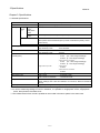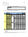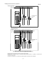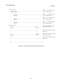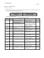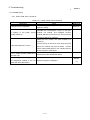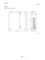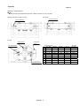
1
Insulation Monitoring Module Changes for the Better User’s Manual (Details) MODEL QE82LG Thank you for purchasing the Mitsubishi MELSEC-Q series programmable controllers. Before using this product, please read this manual carefully and pay full attention to safety to handle the product correctly. Mitsubishi Programmable Controller MODEL MODEL CODE QE82LG-U-SY-E 19H871 IB63564-C C 2013 MITSUBISHI ELECTRIC CORPORATION IB63564-C ● SAFETY PRECAUTIONS ● (Read these precautions before using this product.) This manual contains important instructions for MELSEC-Q series QE82LG. Before using this product, please read this manual and the relevant manuals carefully and pay full attention to safety to handle the product correctly. The precautions given in this manual are concerned with this product only. For the safety precautions of the programmable controller system, refer to the user’s manual of the CPU module used. In this manual, the safety precautions are classified into two levels: "DANGER" and "CAUTION". DANGER Indicates that incorrect handling may cause hazardous conditions, resulting in death or severe injury. CAUTION Indicates that incorrect handling may cause hazardous conditions, resulting in medium or slight personal injury or physical damage. Under some circumstances, failure to observe the precautions given under “ CAUTION” may lead to serious consequences. Observe the precautions of both levels because they are important for personal and system safety. Keep this manual in an accessible place for future reference whenever needed, and make sure it is delivered to the end user. [Precautions for Operating Environment and Conditions] Caution Do not use this product in the places listed below. Failure to follow the instruction may cause malfunctions or decrease of product-life. - Places the Ambient temperature exceeds the range 0 - 55ºC. - Places the Relative humidity exceeds the range 5 - 95% or condensation is observed. - Altitude exceeds 2000 m. - Places exposed to rain or water drop. - Dust, corrosive gas, saline and oil smoke exist. - Vibration and impact exceed the specifications. - Installation on excluding the control board A-1 [Design Precautions] Danger Do not write data into “System Area” in the buffer memory of the intelligent function module. Also, do not output (turn ON) the “use prohibited” signal in the output signal sent from the sequencer CPU to the intelligent function module. Doing so may cause a malfunction to the sequencer system. Caution Do not install the input signal wire together with the main circuit lines or power cables. Keep a distance of 300 mm or more between them. (Except for the terminal input part) Failure to do so may result in malfunction due to noise. This module can not be used as an Electric Leakage Relay. [Installation Precautions] Caution Any person who is involved in the installation and the wiring of this Sequencer should be fully competent to do the work. Use the programmable controller in an environment that meets the general specifications in the User’s manual of the CPU module used. Failure to do so may result in electric shock, fire, malfunction, or damage to or deterioration of the product. To mount the module, while pressing the module-mounting lever located in the lower part of the module, fully insert the module fixing projection(s) into the hole(s) in the base unit and press the module until it snaps into place. Incorrect mounting may cause a malfunction, failure or a fall of the module. When using the Sequencer in an environment of frequent vibrations, fix the module with a screw. Tighten the screws within the specified torque range. Fixing-Module screw (arranged by user): M3 x 12mm Tightening torque of the fixing-module screws 0.36 - 0.48 N•m When the screw tightening is loose, it causes a fall, short-circuit, and a malfunction. Over-tightening can damage the screws and the module, and it may cause a fall, short-circuit, or a malfunction. Shut off the external power supply for the system in all phases before mounting or removing the module. Failure to do so may result in damage to the product. Do not touch directly any conductive parts and electronic parts of the module. Doing so can cause a malfunction or failure of the module. A-2 [Wiring Precautions] Danger For installation and wiring works, make sure that the power source is shut off for all outside phases. If all phases are not turned off, it may cause an electric shock or product damages. Caution FG terminal must be grounded according to the D-type ground (Type 3) dedicated for sequencer. Failure to do so may result in electric shock or malfunction. When using this product, make sure to use it in combination with Mitsubishi’s zero-phase current transformer (ZCT). Please not to exceed the ratings of this product for input of zero phase transformer. For further details, please refer to zero phase transformer manual to maintain the functionality and the accuracy of this product . Split-type ZCT Through-type ZCT CZ-22S , CZ-30S , CZ-55S CZ-77S , CZ-112S ZT15B, ZT30B , ZT40B , ZT60B , ZT80B , ZT100B , ZTA600A , ZTA1200A , ZTA2000A This module and the zero-phase current transformer are used for less than 600V circuit only. They are not used with exceeding 600V circuit. Do not open the secondary side of the zero-phase current transformer. Take care not entering any foreign objects such as chips and wire pieces into the module. It may cause a fire, failure or a malfunction. In order to prevent the module from incoming foreign objects such as wire pieces during wiring work, a foreign-object preventive label is placed on the module. While a wiring work is performed, keep the label on the module. Before operating the system, peel off the label for heat release. If the foreign-object preventive label is not peeled and the system is in use, residual heat inside the module may reduce the product life. The wires to be connected to the module shall be put in a duct or fixed together by clamp. If not, the loosing and unstable wire or careless stretching results in poor contact of electric wires. That may cause a breakage of the module or wire or a malfunction. Use appropriate size of electric wires. If inappropriate size of electric wire is used, it may cause a fire due to generated heat. For appropriate size of electric wires, refer to 7.4.2 How to connect wires ( P7-6). In case using stranded wire, take measures so that the filament should not vary by using a bar terminal or by processing the point twisted. Use the bar terminal appropriated for the size of electric wires. If using inappropriate bar terminals, a wire breakage or a contact failure may cause a device malfunction, failure, a burnout or a fire. After wiring, confirm whether there is a wiring forgetting or a faulty wiring. They may cause a device malfunction, a fire, or an electric shock. When removing the wires connected to the module, do not pull wires as holding on their electric wire portions. Push the buttons on the terminal, and then remove the wire. If the wires connected to the module are strongly pulled off, it may cause a malfunction or a breakage to the module or the wire. (Tensile load: 22N or less) Ensure the wiring to the module properly, checking the rated voltage and current of the product and the terminal pin assignment. If the input voltage exceed the rated voltage or the wiring is improper, it may cause a fire or a breakage. Do not exceed the specified voltage when doing an insulation resistance test and a commercial frequency withstand voltage test. A-3 [Start-up Precautions] Caution Use the product within the ratings specified in this manual. When using it outside the ratings, it not only causes a malfunction or failure but also there is a fear of igniting and damaging by a fire. Before operating the product, check that active bare wire and so on does not exist around the product. If any bare wire exists, stop the operation immediately, and take an appropriate action such as isolation protection. Do not disassemble or modify the module. It may cause failure, a malfunction, an injury or a fire. Attaching and detaching the module must be performed after the power source is shut off for all outside phases. If not all phases are shut off, it may cause failure or a malfunction of the module. Do not touch the live terminal. It may cause a malfunction. [Maintenance Precautions] Caution Cleaning and additional tightening of module-fixing screws must be performed after the input power source is shut off for all outside phases. If not all phases are shut off, it may cause failure or a malfunction of the module. Use a soft dry cloth to clean off dirt of the module surface. Do not let a chemical cloth remain on the surface for an extended period nor wipe the surface with thinner or benzene. Check for the following items for using this product properly for long time. <Daily maintenance> (1) No damage on this product (2) No abnormality with LED indicators (3) No abnormal noise, smell or heat. <Periodical maintenance> (Once every 6 months to 1 year) (4) Confirm there is loosing in installation, wire connection to terminal blocks, and the connection of the connectors. (Check these items under the power failure condition.) [Storage Precautions] Caution To store this product, turn off the power and remove wires, and put it in a plastic bag. For long-time storage, avoid the following places. Failure to follow the instruction may cause a failure and reduced life of the product. - Places the Ambient temperature exceeds the range -25 to +75ºC. - Places the Relative humidity exceeds the range 5 - 95% or condensation is observed. - Dust, corrosive gas, saline and oil smoke exist, and vibration and frequent physical impact occur. - Places exposed to rain or water drop. [Disposal Precautions] Caution Dispose of the product as an industrial waste. A-4 Revision history * Manual number is provided at the bottom of the cover page. Printed date * Manual number Jan, 2011 IB-63564 Revision history First edition Sep, 2011 IB-63564-A Correction SAFETY PRECAUTIONS, Section 4.2, Section 8.1, Section 8.3 Addition SAFETY PRECAUTIONS, Section 2.1, Section 3.2, Section 7.4, Section 9.3 Aug. 2012 IB-63564-B Correction Section 2.3, Section 7.6, Section 9.1 Jul. 2013 IB-63564-C Correction Section 2.3, Section 7.6, Section 7.7, Section 8.2, Section 9.3 Addition Section 1.1, Section 3.1, Section 4.2, Section 6.1, Section 6.3 This manual does not guarantee to protect or does not give a permission to any industrial property and any related rights. Also, our company shall not be held any responsible for any issues related to industrial properties due to product usage described in this manual. 2011 MITSUBISHI ELECTRIC CORPORATION A-5 Table of Content SAFETY PRECAUTIONS··································································································································A-1 Revision history ··················································································································································A-5 Table of content··················································································································································A-6 Compliance with the EMC and Low Voltage Directives····················································································A-8 Names, abbreviations, terminology ··················································································································A-9 Product configuration ·········································································································································A-9 Chapter 1: Overview 1-1 1.1 Features ······················································································································································· 1-1 Chapter 2: System Configuration 2-1 - 2-4 2.1 Applicable system ········································································································································ 2-1 2.2 Precautions for system configuration ·········································································································· 2-2 2.3 How to check the function version, serial number, and module version ···················································· 2-3 Chapter 3: Specifications 3-1 - 3-3 3.1 General specifications·································································································································· 3-1 3.2 Electrical and mechanical specifications ····································································································· 3-2 Chapter 4: Functions 4-1 - 4-11 4.1 List of functions············································································································································· 4-1 4.2 Functions in detail ······································································································································· 4-2 4.2.1 Measuring functions ······························································································································ 4-2 4.2.2 Max. value hold function························································································································ 4-3 4.2.3 Alarm monitoring function ···················································································································· 4-4 4.2.4 Alarm occurrence count function ······································································································ 4-10 4.2.5 Test function ········································································································································ 4-11 Chapter 5: I/O signal to CPU module 5-1 - 5-7 5.1 List of I/O signals·········································································································································· 5-1 5.2 Details of I/O signals ···································································································································· 5-2 5.2.1 Input signals··········································································································································· 5-2 5.2.2 Output signals········································································································································ 5-5 Chapter 6: Buffer memory 6-1 - 6-12 6.1 Buffer memory assignment·························································································································· 6-1 6.2 Configurable sections (Un\G0 to Un\G1100, Un\G2000 to Un\G2100) ···················································· 6-4 6.3 Measurable sections (Un\G1100 to Un\G1999, Un\G2100 to Un\G2999)················································ 6-6 6.4 Common sections (Un\G3000 to Un\G4999) ··························································································· 6-11 A-6 7-1 - 7-16 Chapter 7: Setting and procedure for operation 7.1 Precautions for handling ···························································································································· 7-1 7.2 Procedure for operation ····························································································································· 7-2 7.3 Name and function of each part··················································································································· 7-3 7.4 Attaching and removing the module ············································································································ 7-5 7.5 Wiring···························································································································································· 7-6 7.6 Setting from GX Developer ······················································································································ 7-12 Chapter 8: Programming 8-1 - 8-8 8.1 Programming procedure ···························································································································· 8-1 8.2 System configuration and usage conditions for sample program ····························································· 8-2 8.3 Sample programming ································································································································· 8-4 Chapter 9: Troubleshooting 9-1 - 9-7 9.1 List of error codes ······································································································································· 9-1 9.2 Troubleshooting············································································································································ 9-3 9.3 Q&A ······························································································································································ 9-6 Appendix Appendix 1 - 3 Appendix 1: External dimensions ·········································································································Appendix-1 Appendix 2: Optional devices ···············································································································Appendix-2 Index Index 1 A-7 Compliance with the EMC and Low Voltage Directives (1) For programmable controller system To configure a system meeting the requirements of the EMC and Low Voltage Directives when incorporating the Mitsubishi programmable controller (EMC and Low Voltage Directives compliant) into other machinery or equipment, refer to Chapter 9 "EMC AND LOW VOLTAGE DIRECTIVES" of the QCPU User's Manual (Hardware Design, Maintenance and Inspection). The CE mark, indicating compliance with the EMC and Low Voltage Directives, is printed on the rating plate of the programmable controller. (2) For the product For the compliance of this product with the EMC and Low Voltage Directives, refer to Section 7.5 Wiring. (3) CE marking conformity combination module This module conforms to CE marking standard in a condition to make combination use with following zero-phase current transformer (ZCT) and cable. Split-type ZCT Through-type ZCT cable Max. cable length CZ-22S , CZ-30S , CZ-55S CZ-77S , CZ-112S ZT15B, ZT30B , ZT40B , ZT60B , ZT80B , ZT100B , ZTA600A , ZTA1200A , ZTA2000A CE marking cable (twisted pair cable ) Single wire: φ0.5 - 1.2mm Stranded wire: 0.5 - 1.3 mm2 50m A-8 Names, abbreviations, terminology In this manual, the following names, abbreviations, and terminology are used to explain the insulation monitoring module, unless otherwise specified. Names, abbreviations, terminology Io1 Ior1 Io2 Ior2 CH1 Alarm CH2 Alarm CH1 max. value CH2 max. value Date/time of occurrence CH1 Alarm occurrence count CH2 Alarm occurrence count ZCT Descriptions of names, abbreviations, terminology Abbreviation for CH1 leak current. Abbreviation for CH1 leak current for resistance. Abbreviation for CH2 leak current. Abbreviation for CH2 leak current for resistance. Collective term for Io1 1-step alarm, Io1 2-step alarm, Ior1 1-step alarm, and Ior1 2-step alarm. Collective term for Io2 1-step alarm, Io2 2-step alarm, Ior2 1-step alarm, and Ior2 2-step alarm. Collective term for Io1 max. value and its date/time of occurrence, and Ior1 max. value and its date/time of occurrence. Collective term for Io2 max. value and its date/time of occurrence, and Ior2 max. value and its date/time of occurrence. Collective term for the year of max. value occurrence, month and day of max. value occurrence, hour and minute of max. value occurrence, and second and day of the week of max. value occurrence. Collective term for Io1 1-step alarm occurrence count, Io1 2-step alarm occurrence count, Ior1 1-step alarm occurrence count, and Ior1 2-step alarm occurrence count. Collective term for Io21 1-step alarm occurrence count, Io2 2-step alarm occurrence count, Ior2 1-step alarm occurrence count, and Ior2 2-step alarm occurrence count. Abbreviation for zero-phase current transformer Product configuration The following describes the product configuration. Model name QE82LG Product name Insulation monitoring Module Quantity 1 A-9 Note A - 10 1 Overview QE82LG Chapter 1: Overview This manual explains specifications, handling methods, and programming of Insulation Monitoring Module QE82LG (hereinafter, abbreviated as QE82LG) supporting MELSEC-Q series. 1.1 Features (1) This enables to measure leak current for safety actions. By monitoring leak current (Io), risk for electric shock can be detected. (2) This enables constant monitoring of insulation for equipment. By monitoring leak current for resistance (Ior), deterioration of equipment insulation can be tracked. (3) This enables 2-level alarm monitoring during monitoring for each measuring element. For each leak current (Io) and leak current for resistance (Ior), 2-level alarm monitoring can be performed without a sequence. (4) This enables to measure two circuits, using one device. At the power source with the same-phase wire system, a single device can measure two circuits. (5) This enables to measure sensitive. By changing setting to high sensitivity mode, this enables to measure from 0.01mA. 1-1 2 System Configuration QE82LG Chapter 2: System Configuration 2.1 Applicable system The following describes applicable systems. (1) Applicable module and the quantity of attachable pieces CPU module to which QE82LG can be attached and the number of attachable pieces are shown below. Depending on the combination of the attached module and the number of attached pieces, lack of power capacity may occur. When attaching the module, please consider the power capacity. If the power capacity is insufficient, reconsider the combination of modules to be attached. Remarks Attachable Attachable CPU Module CPU Type Programmable controller CPU CPU Model Q00JCPU Basic model Q00CPU QCPU Q01CPU Q02CPU High performance Q02HCPU Q06HCPU model QCPU Q12HCPU Q25HCPU Q02PHCPU Q06PHCPU Process CPU Q12PHCPU Q25PHCPU Q12PRHCPU Redundant CPU Q25PRHCPU Q00UJCPU Q00UCPU Q01UCPU Q02UCPU Q03UDCPU Q04UDHCPU Q06UDHCPU Q10UDHCPU Q13UDHCPU Universal model Q20UDHCPU QCPU Q26UDHCPU Q03UDECPU Q04UDEHCPU Q06UDEHCPU Q10UDEHCPU Q13UDEHCPU Q20UDEHCPU Q26UDEHCPU Q50UDEHCPU Q100UDEHCPU Q03UDVCPU Q04UDVCPU High-Speed Universal model Q06UDVCPU QCPU Q13UDVCPU Q26UDVCPU 2-1 quantity. 16 24 64 64 53 16 24 36 64 64 2 System Configuration QE82LG Attachable CPU Module CPU Type Attachable CPU Model Q06CCPU-V Q06CCPU-V-B Q12DCCPU-V C Controller module Remarks quantity. 64 (2) Attachable base unit QE82LG can be attached to any I/O slot of the basic base unit and expansion base unit (*1) (*2). *1 In the case of dual CPU, it can be attached only to an expansion base unit. It cannot be attached to the base unit. *2 It has to be within the range of I/O slots of the CPU module. (3) Applicable software package QE82LG supported software packages are as follows: (a) Software package for sequencer Product name Model name Remarks Sequencer engineering software GX Works2 SWnDNC-GXW2 “n” in the model name is 1 or larger. MELSEC sequencer programming software. GX Developer SWnD5C-GPPW “n” in the model name is 4 or larger. 2.2 Precautions for system configuration (1) When attaching it to an expansion base without a power module If QE82LG is attached to an expansion base without a power module, refer to the user’s manual of the sequencer CPU to be used in order to select the power module and expansion cable. 2-2 2 System Configuration QE82LG 2.3 How to check the function version, serial number, and module version (1) How to check the serial number and module version It can be checked with the serial number label (placed on the right side of QE82LG). Module version 19H101 710G1234 Serial No. Barcode (2) How to check the function version and serial number (a) Checking on the front of the module. The serial number and function version on the rating plate is shown on the front (at the bottom) of the module. Function version Serial number 2-3 2 System Configuration QE82LG (b) Checking on the System monitor dialog box (Product Information List) To display the system monitor, select [Diagnostics] → [System monitor] and click the Product Information List button of GX Developer. Point The serial number displayed on the Product Information List dialog box of GX Developer may differ from that on the rating plate and on the front of the module. ・ The serial number on the rating plate and front part of the module indicates the management information of the product. ・ The serial number displayed on the Product Information List dialog box of GX Developer indicates the function information of the product. The function information of the product is updated when a new function is added. 2-4 3 Specifications QE82LG Chapter 3: Specifications 3.1 General specifications Item Phase-wire system Ratings Voltage single-phase circuit 2-wire, *1,*2 three-phase 3-wire single-phase 3-wire Leak current circuit Frequency Measuring range Resolution Allowable tolerance of module (excluding ZCT) Measurable circuit count Data update cycle Backup for electric blackout I/O occupation Specifications single-phase 2-wire / single-phase 3-wire / three-phase 3-wire 110 V , 220 V AC 110V AC (1 - 2 line, 2 - 3 line) 220 V (1 - 3 line) 1 A AC (Zero-phase current transformer (ZCT) is used. It indicates the primary current value of ZCT.) 50-60 Hz Low sensitivity mode : 0-1000mA High sensitivity mode : 0.00-100.00mA Low sensitivity mode : 1mA High sensitivity mode : 0.01mA Low sensitivity mode : Leak current : ±2.5% (10 – 100% range of Ratings) : ±2.5mA (0 – 10% range of Ratings) : Leak current for resistance : ±2.5% (10 – 100% range of Ratings) : ±2.5mA (0 – 10% range of Ratings) High sensitivity mode : Leak current : ±2.5mA : Leak current for resistance : ±2.5mA 2 circuits*3 : 2 seconds or less Leak current : 10 seconds or less Leak current for resistance Nonvolatile memory is used. (Items: Settings, Max. value and date/time of occurrence, Alarm occurrence count) 16 points (I/O assignment: intelligence 16 points) * 1:110 V, 220V direct connection is possible. Above 440V voltage transformer outside (VT) is required. * 2:In case of measuring leakage current for resistance, it is possible on single-phase 2-wire, single-phase 3-wire, three-phase 3-wire delta circuit. * 3:The measurement of two circuits is possible at one module in the same system in the same trans. 3-1 3 Specifications QE82LG 3.2 Electrical and mechanical specifications Item Consumption Voltage VA circuit Internal current consumption (5 V DC) Operating temperature Operating humidity Storage temperature Storage humidity Operating altitude Installation area Operating environment Vibration resistance Specifications Each phase 0.1 VA (at 110 V AC), Each phase 0.2 VA (at 220 V AC) 0.17 A 0 – 55°C (Average daily temperature 35°C or below) 5 – 95% RH (No condensation) -25° – +75°C 5 – 95% RH (No condensation) 2000m or below Inside a control panel No corrosive gas Constant Conforms to JIS Frequency acceleration B 3502, IEC 61131-2 5 – 8.4 Hz Intermittent vibration Impact resistance Over voltage category *1 Pollution degree *2 Equipment category Applicable ZCT Input wire terminal (Usable (Z+, Z terminal)*3 electric Voltage input *6 wire) terminal Tightening torque Commercial frequency withstand voltage Half amplitude 3.5 mm 9.8 m/s2 - Continuous 5 – 8.4 Hz - 1.75 mm vibration 8.4 – 150 Hz 2 4.9 m/s XYZ each direction 8.4 – 150 Hz 2 Sweep time 10 times - - Conforms to JIS B 3502, IEC 61131-2 (147 m/s , XYZ each direction 3 times) II or less 2 or less Class I φ0.5 – 1.2 mm Single wire 2 *4 0.5 – 1.3 mm Stranded wire φ0.5 – 1.2 mm Single wire 2 *4 0.5 – 1.3 mm Stranded wire *5 Module-fixing screws (M3 screw) 0.36 – 0.48 N・m Between voltage/leak current input terminals – FG terminal 2210 V AC 5 sec 2210 V AC 5 sec Between voltage/leak current input terminals – sequencer power source and GND terminal 5 MΩ or more (500 V DC) at locations above Insulation resistance 27.4 mm (W) x 98 mm (H) x 90 mm (D), excluding protruding portions External dimensions 0.1 kg Mass 10 years (used under the average daily temperature 35°C or less) Product life expectancy *1. This indicates the assumed area of electric distribution to which the device is connected, the area ranging from public distribution to factory machinery. The category II applies to the device power-supplied from fixed facility. The surge voltage of this product is 2500 V up to the rated voltage of 300 V. *2. The index indicates the level of conductive substance at the device’s operating environment. Contamination level 2 means only non-conductive substance. However, occasional condensation may lead to temporary conduction. *3. At the connection between ZCT secondary terminal and this module terminal (Z+, Z), each wire has to be twisted for usage. *4. If stranded wire is used, a bar terminal must be used. Recommended bar terminal: TGV TC-1.25-11T (Made by Nichifu) *5. The module can be fixed easily to the base unit, using the hook on top of the module. However, if it is used under a vibrating environment, we strongly recommend that the module be fixed with screws. 3-2 3 Specifications QE82LG *6. UL / C-UL listed corresponds , use the wires according to the following conditions. Single wire: AWG24~AWG18, Stranded wire: AWG20~AWG18.60/75℃ copper conductor only. 3-3 4 Functions QE82LG Chapter 4: Functions 4.1 List of functions Functions of QE82LG are provided in Table 4.1-1. Table 4.1-1 List of functions No. Function Reference Descriptions section It enable measures Io1, Ior1, Io2, and Ior2, and stores the records into a buffer memory as needed. 1 Section 4.2.1 Measurement It changes a low sensitivity mode (0-1000mA) and high Section sensitivity mode (0.00-100.00mA) and can measure an 7.6.2 leak current. 7.7.2 For Io1, Ior1, Io2, and Ior2, each maximum values and date of occurrence are stored in the buffer memory as 2 Hold max. values needed. Even if the power source reset occurs, maximum values Section 4.2.2 and date of occurrence are retained. It can monitor the upper limit for Io1,Ior1,Io2, and Ior2. In addition, you can set 2 steps of alarm values for each monitored element, and they can be used in such way to 3 Alarm monitoring release cautious alarm and real alarm. When the value exceeds and continues to be over the monitoring value Section 4.2.3 for alarm delay time, a specified input signal is turned on. For each alarm monitored element, it counts the frequency of the alarms, which will be stored in the buffer memory as needed. 4 Alarm occurrence It can count up to 9999 times of Alarm occurrence count. Section count If the count exceeds 9999 times, Alarm occurrence 4.2.4 count remains 9999 times. Even if the power source reset occurs, the count of alarm occurrence is retained. The intelligent function module switch enables pseudo-storage of the specified value into the buffer 5 Test memory, even with non-existence of voltage and current (sensor) input. Using this module, you can create a sequence, etc. 4-1 Section 4.2.5 4 Functions QE82LG 4.2 Functions in detail 4.2.1 Measuring functions (1) Measured items Measured items and measured ranges are described as follows: Measured items Details CH1 leak current Present value (Un\G1100) Max. value (Un\G1101) Date/time of occurrence (Un\G1102 to Un\G1105) CH1 leak current for resistance Present value (Un\G1150) Max. value (Un\G1151) Date/time of occurrence (Un\G1152 to Un\G1155) CH2 leak current Present value (Un\G2100) Max. value (Un\G2101) Date/time of occurrence (Un\G2102 to Un\G2105) CH2 leak current for resistance Present value (Un\G2150) Max. value (Un\G2151) Date/time of occurrence (Un\G2152 to Un\G2155) (2) Resolution of measured data Resolution of measured data is described as follows: - Leak current, leak current for resistance Mode Measured items Io1 Ior1 Io2 Ior2 Resolution Measuring range Low sensitivity mode Integer 1 mA 0-1000mA High sensitivity mode Two decimal places 0.01mA 0.00-100.00mA (3) Restrictions for measuring data - Measurement cannot be performed immediately after the power loading to the sequencer system (while Module ready (Xn0) is under the OFF condition). After checking that Module ready (Xn0) is ON, obtain measuring data. - Measurement cannot be performed immediately after operating conditions are set up to this module. After checking that Operating condition setting completion flag (Xn9) becomes ON, obtain measuring data. - Behaviors during operation are as follows: Measured items Behavior of this module Io1 Ior1 Io2 Ior2 When the input current is less than 1 mA in low sensitivity mode or 0.01mA in high sensitivity mode, it becomes 0 mA. When the input current is less than 80 V, it becomes 0 mA. In the case of abnormal frequency (when it is less than 44.5 Hz 4-2 4 Functions QE82LG or over 66.5 Hz), it becomes 0 mA. 4-3 4 Functions QE82LG 4.2.2 Max. values hold function It memorizes the max. value for each measured element, and retains it until the max. value is cleared. (1) Max. value memory 1) It memorizes the max. value for the following measured element. - CH1 leak current - CH1 leak current for resistance - CH2 leak current - CH2 leak current for resistance 2) It memorizes the date and time of occurrence (year/month/day/hour/minute/second/day of the week) together with the max. value. 3) The max. value and the date and time of occurrence are stored in the nonvolatile memory, so that these max. values can be retained even at a power source reset. (2) How to clear the max. value 1) You can use the I/O signal to clear the max. value. 2) The max. value immediately after clearing will be the present value and the date of occurrence will be the present date and time. 3) The following data can be cleared upon CH1 max. value clear request (YnA). However, the following data cannot be cleared individually. - Io1 max. value (Un\G1101) - Io1 date and time of occurrence (Un\G1102 to Un\G1105) - Ior1 max. value (Un\G1151) - Ior1 date and time of occurrence (Un\G1152 to Un\G1105) 4) The following data can be cleared upon CH2 max. value clear request (YnC). However, the following data cannot be cleared individually. - Io2 max. value (Un\G2101) - Io2 date and time and time of occurrence (Un\G2102 to Un\G2105) - Ior2 max. value (Un\G2151) - Ior2 date and time of occurrence (Un\G2152 to Un\G2105) 5) The following describes how to clear CH1 max. value. (CH2 max. value follows the same procedure using CH2 max. value clear request (YnC).) (i) Check that CH1 max. value clear request (YnA) is OFF. (ii) Set CH1 max. value clear request (YnA) to ON. Max. values and dates and times of occurrence of CH1 leak current and CH1 leak current for resistance are cleared, and then CH1 max. value clear completion flag (XnA) is turned ON. (iii) Check that CH1 max. value clear completion flag (XnA) is ON, and then set CH1 max. value clear request (YnA) to OFF. CH1 max. value clear request (YnA) CH1 max. value clear completion flag (XnA) Figure 4.2.2-1 Procedure for clearing max. value 4-4 4 Functions QE82LG 4.2.3 Alarm monitoring function For monitoring each measured item, you can set max. 2 points of upper limit alarm to perform monitoring. During the alarm monitoring, the module can monitor the input signal to check for the occurrence. (1) Setting the alarm monitoring 1) Setting items and setting range for the alarm monitoring are described below. Setting item Setting range Alarm value Low sensitivity mode 1 to 1000 (mA) High sensirivity mode 0.01-100.00 (mA) 0: No monitoring Alarm reset method 0: Self-retention 1: Auto reset Alarm delay time 0 to 300 (seconds) Description The value is for monitoring the target measured element. Alarm is released when the present value exceeds alarm value and the situation continues for alarm delay time. Also, in the case of 2-step monitoring, the 1-step and secondary alarm values can be configured regardless of their size. You can set whether or not the alarm-occurrence condition should be retained if the value goes back to the alarm value after the alarm is released. Alarm is released when the present value exceeds the alarm value and the situation continues for alarm delay time. 2) Setting procedures are as follows: (i) Check that Operating condition setting request (Yn9) is OFF. (ii) Set alarm value, alarm reset method, and alarm delay time. For the address of buffer memory corresponding to each measured element, refer to Chapter 6. (iii) Set Operating condition setting request (Yn9) to ON. Operation starts at each set value, and then Operating condition setting completion flag (Xn9) is turned OFF. (iv)Check that Operating condition setting completion flag (Xn9) becomes OFF, and then set Operating condition setting request (Yn9) to OFF. Operating condition setting request (Yn9) Operating condition setting completion flag (Xn9) Figure 4.2.3-1 Time chart of alarm monitoring setting 3) Each item of the alarm monitoring is stored in the nonvolatile memory, so that set values can be retained even at a power source reset. 4-5 4 Functions QE82LG (2) Alarm flag (Xn1 to Xn8) and behavior of ALM1 LED and ALM2 LED 1) There are 4 statuses of alarm for each alarm monitoring element. (a) Alarm non-occurrence status The present value is under alarm value or the present value exceeds alarm value but the situation continues for less than alarm delay time. (b) Alarm occurrence status The present value exceeds alarm value and the situation exceeds alarm delay time. (c) Self-retention status (Only when the alarm reset method is set to “self-retention”) The present value has changed from the alarm occurrence status to be under alarm value. (d) Alarm reset status Alarm reset request (Yn1, Yn5) is released under the alarm occurrence status, and the present value is still over alarm value. * In order to state the alarm, alarm monitoring must be less than the value once during the alarm reset state. Alarm value Alarm mask time Alarm mask time Alarm mask time Io1 primary alarm flag (Xn1) Request of CH1 alarm reset (Yn1) Alarm status Alarm non-occurrence Alarm occurrence Self-retention Alarm occurrence Alarm reset Alarm non-occurrence Figure 4.2.3-2 Example of alarm status (alarm reset method = “self-retention”) 2) Relationship between the alarm status and Alarm flag (Xn1 to Xn8) (a) Alarm non-occurrence status Under the alarm non-occurrence status, Alarm flag (Xn1 to Xn8) is OFF. (b) Alarm occurrence status Under the alarm occurrence status, Alarm flag (Xn1 to Xn8) is ON. (c) Self-retention status Under the self-retention status, Alarm flag (Xn1 to Xn8) is ON. (d) Alarm reset status Under the alarm reset status, Alarm flag (Xn1 to Xn8) is OFF. 4-6 Alarm occurrence 4 Functions QE82LG 3) Behaviors of ALM1 LED and ALM2 LED (a) The indication of ALM1 LED changes according to status of CH1 Alarm. Io1 primary alarm flag (Xn1) Io1 secondary alarm flag (Xn2) Ior1 primary alarm flag (Xn3) Ior1 secondary alarm flag (Xn4) (b) The indication of ALM2 LED changes according to status of CH2 Alarm. Io2 primary alarm flag (Xn5) Io2 secondary alarm flag (Xn6) Ior2 primary alarm flag (Xn7) Ior2 secondary alarm flag (Xn8) (c) ALM1 LED and ALM2 LED display the following 3 indications according to the alarm status of the alarm occurrence flag. - Flashing Of the alarm occurrence flags, one or more flags are in the alarm occurrence status or in the alarm reset status (regardless of the status of the remaining alarm occurrence flags). - ON Of the alarm occurrence flags, one or more flags are in the self-retention status and the remaining flags of alarm occurrence are in the alarm non-occurrence status. - OFF Flags of alarm occurrence are all in the alarm non-occurrence status. 4-7 4 Functions QE82LG (3) Behavior of alarms 1) When the alarm reset method is in the “auto reset” setting (Example of Io1 primary alarm monitoring): (a) If the present value Io1 exceeds alarm value and the situation continues for alarm delay time, Io1 primary alarm flag (Xn1) will be turned ON. At the same time, ALM1 LED flashes. (b) If the present value goes below the upper limit, Io1 primary alarm flag (Xn1) will be turned OFF. At this time, ALM1 LED is turned off. (c) Even if the present value Io1 exceeds alarm value, if the value goes under alarm value within alarm delay time, Io1 primary alarm flag (Xn1) will remain OFF. Alarm value 警報監視値 警報マスク時間 Alarm mask time 警報マスク時間 Alarm mask time ON CH1漏洩電流一段警報 Io1 primary alarm flag (Xn1) 発生フラグ(Xn1) ALM1 LED OFF OFF OFF 消灯 Flashing 点滅 (a) OFF 消灯 (c) (b) Figure 4.2.3-3 Time chart of the secondary alarm (alarm reset method = “auto-reset”) 2) When alarm reset method is set to “self-retention” (Example of Io1 primary alarm monitoring) (a) If the present value Io1 exceeds alarm value and the situation continues for alarm delay time, Io1 primary alarm flag (Xn1) will be turned ON. At the same time, ALM1 LED flashes. (b) If the present value Io1 goes below the upper limit, Io1 primary alarm flag (Xn1) remains ON (self-retention). During the self-retention, ALM1 LED is turned on. (c) By turning CH1 alarm reset request (Yn1) to ON, Io1 primary alarm flag (Xn1) will be turned OFF. At this time, ALM1 LED is turned off. (d) Check that Io1 primary alarm flag (Xn1) becomes OFF, and then set CH1 alarm reset request (Yn1) to OFF. Alarm value Alarm mask time Io1 primary alarm flag (Xn1) CH1 alarm reset request (Yn1) OFF Flashing ON OFF Figure 4.2.3-4 Time chart of the secondary alarm (alarm reset method = “self-retention”) 4-8 4 Functions QE82LG 3) An example of Io1 primary alarm monitoring is indicated in 1) and 2) above. Other alarm monitoring will be in accordance with the same behavior. For the setting items for the buffer memory that corresponds to the alarm monitoring and the I/O signals, refer to Chapters 5 and 6. (3) How to reset Alarm flag 1) If Alarm flag is ON during the alarm occurrence or the self-retention (in the case of the alarm reset method = “self-retention”), Alarm flag can be reset (turned OFF) using Alarm reset request. 2) CH1 alarm clear request (Yn1) will clear the following data. However, the following data cannot be cleared individually. - Io1 primary alarm flag (Xn1) - Io1 secondary alarm flag (Xn2) - Ior1 primary alarm flag (Xn3) - Ior1 secondary alarm flag (Xn4) 3) The following data can be cleared upon CH2 alarm reset request (Yn5). However, the following data cannot be cleared individually. - Io2 primary alarm flag (Xn5) - Io2 secondary alarm flag (Xn6) - Ior2 primary alarm flag (Xn7) - Ior2 secondary alarm flag (Xn8) 4-9 4 Functions QE82LG 4) How to reset Alarm flag during alarm occurrence (Example of Io1 primary alarm monitoring) (a) If the present value Io1 exceeds alarm value, Io1 primary alarm flag (Xn1) will be turned ON. At the same time, ALM1 LED flashes. (b) By turning CH1 alarm reset request (Yn1) to ON, Io1 primary alarm flag (Xn1) will be turned OFF. At this time, ALM1 LED will remain flashing (because ALM1 LED is synchronized with the alarm status, it will not turn off). (c) Check that Io1 primary alarm flag (Xn1) becomes OFF, and then set CH1 alarm reset request (Yn1) to OFF. (d) If the present value Io1 goes under alarm value, ALM1 LED will be turned off. (e) After that, if the present value Io1 exceeds alarm value, Io1 primary alarm flag (Xn1) will be turned ON again. At the same time, ALM1 LED flashes. 警報監視値 Alarm value 警報マスク Alarm 時間time mask lo1 primary alarm flag (Xn1) 警報マスク Alarm 時間time mask ON Io1一段警報発生フラグ CH1 alarm reset request (Yn1) (Xn1) CH1警報リセット要求 (Yn1) ALM1 LED ON OFF OFF ON OFF OFF OFF 消灯 Flashing 点滅 (a) (b) (c) OFF 消灯 (d) Flashing 点滅 (e) Figure 4.2.3-5 Procedure for resetting Io1 primary alarm flag (alarm reset method = “auto-reset”) 5) How to reset Alarm flag during self-retention (in the case the alarm reset method = “self-retention” only) Refer to the procedure described in (2) 2). 4 - 10 4 Functions QE82LG 4.2.4 Alarm occurrence count function It memorizes the count of alarm occurrence for each alarm monitoring element, and retains it until the count of alarm occurrence is performed. (1) Memory of Alarm occurrence count 1) It memorizes each alarm occurrence count for the following element. - Io1 primary alarm - Io1 secondary alarm - Ior1 primary alarm - Ior1 secondary alarm - Io2 primary alarm - Io2 secondary alarm - Ior2 primary alarm - Ior2 secondary alarm 2) Alarm occurrence count is stored in the nonvolatile memory, so that it can be retained even at a power source reset. (2) How to clear Alarm occurrence count 1) You can use I/O signal to clear the count of alarm occurrence. 2) The count of alarm occurrence immediately after the clear will be “0”. 3) The following data can be cleared upon CH1 alarm occurrence count clear request (YnB). However, the following data cannot be cleared individually. - Io1 primary alarm occurrence count (Un\G1200) - Io1 secondary alarm occurrence count (Un\G1201) - Ior1 primary alarm occurrence count (Un\G1250) - Ior1 secondary alarm occurrence count (Un\G1251) 4) The following data can be cleared upon CH2 alarm occurrence count clear request (YnD). However, the following data cannot be cleared individually. - Io2 primary alarm occurrence count (Un\G2200) - Io2 secondary alarm occurrence count (Un\G2201) - Ior2 primary alarm occurrence count (Un\G2250) - Ior2 secondary alarm occurrence count (Un\G2251) 5) The following describes how to clear CH1 alarm occurrence count. (CH2 alarm occurrence count follows the same procedure using CH2 alarm occurrence count clear request (YnD).) (i) Check that CH1 alarm occurrence count clear request (YnB) is OFF. (ii) Set CH1 alarm occurrence count clear request (YnB) to ON. CH1 alarm occurrence count is cleared, and then CH1 alarm occurrence count clear completion flag (XnB) is turned ON. (iii) Check that CH1 alarm occurrence count clear completion flag (XnB) is ON, and then set CH1 alarm occurrence count clear request (YnB) to OFF. CH1 alarm occurrence count clear request (YnB) CH1 alarm occurrence count clear completion flag (XnB) Figure 4.2.3-6 Procedure for clearing Alarm occurrence count 4 - 11 4 Functions QE82LG 4.2.5 Test function This function is to output pseudo-fixed value to a buffer memory for debugging sequence program. The value can be output to the buffer memory without input of voltage and current. (1) How to use the test function 1) Using the intelligent function switch settings, you can start the test mode to output the fixed value. 2) For procedure for setting the intelligent function switch, refer to 7.5.2. 3) To finish the test mode, the set value is returned by the intelligent function switch setting, and after that, it starts a measuring mode by resetting it. (It resumes with the previous set value and accumulated electric energy as well as periodic electric energy.) (2) Content of pseudo-output For the value to be output to the buffer memory, refer to Tables 6.1-1 to 6.1-3 in 6.1 Buffer memory assignment. (3) Percolations for using the test function 1) Because pseudo-fixed value is output to the buffer memory, isolate the actual device to avoid unexpected operation before running the sequence program. 4 - 12 5 I/O signal to CPU unit QE82LG Chapter 5: I/O signal to CPU module 5.1 List of I/O signals I/O signals of QE82LG are listed in Table 5.1-1. The “n” that is used in this and later chapters (for example: Xn0, Yn0, Un\G0, etc.) refers to the number that appears at the beginning of QE82LG. Table 5.1-1 List of I/O signals Input signal (signal direction from QE82LG to CPU Output signal(signal direction from CPU module to module) QE82LG) Device # Signal name Device # Signal name Xn0 Module ready Yn0 Use prohibited *1 Xn1 Io1 primary alarm flag Yn1 CH1 alarm reset request Xn2 Io1 secondary alarm flag Yn2 Use prohibited *1 Xn3 Ior1 primary alarm flag Yn3 Use prohibited *1 Xn4 Ior1 secondary alarm flag Yn4 Use prohibited *1 Xn5 Io2 primary alarm flag Yn5 CH2 alarm reset request Xn6 Io2 secondary alarm flag Yn6 Use prohibited *1 Xn7 Ior2 primary alarm flag Yn7 Use prohibited *1 Xn8 Ior2 secondary alarm flag Yn8 Use prohibited *1 Yn9 Operating condition setting request Xn9 XnA XnB XnC XnD Operating condition setting completion flag CH1 max. value clear completion flag CH1 alarm occurrence count clear completion flag CH2 max. value clear completion flag CH2 alarm occurrence count clear completion flag YnA YnB YnC YnD CH1 max. value clear request CH1 alarm occurrence count clear request CH2 max. value clear request CH2 alarm occurrence count clear request XnE Use prohibited *1 YnE Use prohibited *1 XnF Error flag YnF Error clear request Point *1 These signals cannot be used by the user since they are for system use only. If these are set to on or off by the sequence program, the performance of the QE82LG cannot be guaranteed. 5-1 5 I/O signal to CPU unit QE82LG 5.2 Details of I/O signals Detailed explanation about I/O signals of QE82LG is provided as follows: 5.2.1 Input signals (1) Module ready (Xn0) (a) When the power of CPU module is turned on or the CPU module reset is performed, it will turn ON as soon as the measurement is ready. (b) Module ready is turned OFF when the insulation monitoring module displays a hardware error, and RUN LED is turned off. (2) Io1 primary alarm flag (Xn1) (a) When the present value Io1 exceeds Io1 primary alarm value (Un\G1000) and the situation continues for Io1 primary alarm delay time (Un\G1002), this signal (Xn1) turns ON. (b) Operations after this signal (Xn1) is turned ON will be different depending on the setting of Io1 primary alarm reset method (Un\G1001) below. [When Io1 primary alarm reset method (Un\G1001) is “self-retention”] Even if the present value Io1 goes under Io1 primary alarm value (Un\G1000), this signal (Xn1) remains ON. Then, when CH1 alarm reset request (Yn1) is turned to ON, this signal (Xn1) turns OFF. [When Io1 primary alarm reset method (Un\G1001) is “auto reset”] If the present value Io1 goes under Io1 primary alarm value (Un\G1000), this signal (Xn1) turns OFF. (c) When Io1 primary alarm value (Un\G1000) is set to “0 (not monitoring)”, this signal (Xn1) is always OFF. *For the actual behavior of alarm monitoring, refer to 4.2.4. (3) Io1 secondary alarm flag (Xn2) The usage procedure is the same as Io1 primary alarm flag (Xn1). Refer to (2). (4) Ior1 primary alarm flag (Xn3) The usage procedure is the same as Io1 primary alarm flag (Xn1). Refer to (2). (5) Ior1 secondary alarm flag (Xn4) The usage procedure is the same as Io1 primary alarm flag (Xn1). Refer to (2). 5–2 5 I/O signal to CPU unit QE82LG (6) Io2 primary alarm flag (Xn5) The usage procedure is the same as Io1 primary alarm flag (Xn1). Refer to (2). (7) Io2 secondary alarm flag (Xn6) The usage procedure is the same as Io1 primary alarm flag (Xn1). Refer to (2). (8) Ior2 primary alarm flag (Xn7) The usage procedure is the same as Io1 primary alarm flag (Xn1). Refer to (2). (9) Ior2 secondary alarm flag (Xn8) The usage procedure is the same as Io1 primary alarm flag (Xn1). Refer to (2). (10) Operating condition setting completion flag (Xn9) (a) When turning Operating condition setting request (Yn9) to ON and changing the following settings, this signal (Xn9) turns ON. - Phase wire system (Un\G0) - Io1 primary alarm value (Un\G1000) - Io1 primary alarm reset method (Un\G1001) - Io1 primary alarm delay time (Un\G1002) - Io1 secondary alarm value (Un\G1003) - Io1 secondary alarm reset method (Un\G1004) - Io1 secondary alarm delay time (Un\G1005) - Ior1 primary alarm value (Un\G1050) - Ior1 primary alarm reset method (Un\G1051) - Ior1 primary alarm delay time (Un\G1052) - Ior1 secondary alarm value (Un\G1053) - Ior1 secondary alarm reset method (Un\G1054) - Ior1 secondary alarm delay time (Un\G1055) - Io2 primary alarm value (Un\G2000) - Io2 primary alarm reset method (Un\G2001) - Io2 primary alarm delay time (Un\G2002) - Io2 secondary alarm value (Un\G2003) - Io2 secondary alarm reset method (Un\G2004) - Io2 secondary alarm delay time (Un\G2005) - Ior2 primary alarm value (Un\G2050) - Ior2 primary alarm reset method (Un\G2051) - Ior2 primary alarm delay time (Un\G2052) - Ior2 secondary alarm value (Un\G2053) - Ior2 secondary alarm reset method (Un\G2054) - Ior2 secondary alarm delay time (Un\G2055) (b) When Operating condition setting request (Yn9) is OFF, this signal (Xn9) turns OFF. 5–3 5 I/O signal to CPU unit QE82LG (11) CH1 max. value clear completion flag (XnA) (a) When CH1 max. value clear request (YnA) is turned ON and the following max. value data are cleared, this signal (XnA) turns ON. - Io1 max. value (Un\G1101) - Io1 date/time of occurrence (Un\G1102 to Un\G1105) - Ior1 max. value (Un\G1151) - Ior1 date/time of occurrence (Un\G1152 to Un\G1155) (b) When CH1 max. value clear request (YnA) is turned OFF, this signal (XnA) turns OFF. (12) CH1 alarm occurrence count clear completion flag (XnB) (a) When CH1 alarm occurrence count clear request (YnB) is turned ON and the following alarm occurrence count data are cleared, this signal (XnB) turns ON. - Io1 primary alarm occurrence count (Un\G1200) - Io1 secondary alarm occurrence count (Un\G1201) - Ior1 primary alarm occurrence count (Un\G1250) - Ior1 secondary alarm occurrence count (Un\G1251) (b) When CH1 alarm occurrence count clear request (YnB) is turned OFF, this signal (XnB) turns OFF. (13) CH2 max. value clear completion flag (XnC) The usage procedure is the same as CH1 max. value clear completion flag (XnA). Refer to (11). (14) CH2 alarm occurrence count clear completion flag (XnD) The usage procedure is the same as CH1 alarm occurrence count clear completion flag (XnB). Refer to (12). (15) Error flag (XnF) (a) If an outside-set-value error occurs, and if a hardware error occurs, this signal (XnF) turns ON. (b) The description of the error occurred can be checked with latest error code (Un\G3000). *For description of error codes, refer to section 9.1. (c) If an outside-set-value error occurs, this signal (XnF) is turned OFF by setting a value within the range again. 5–4 5 I/O signal to CPU unit QE82LG 5.2.2 Output signals (1) CH1 alarm reset request (Yn1) (a) When resetting the following flags for alarm occurrence, this signal (Yn1) turns ON. - Io1 primary alarm flag (Xn1) - Io1 secondary alarm flag (Xn2) - Ior1 primary alarm flag (Xn3) - Ior1 secondary alarm flag (Xn4) (b) When this signal (Yn1) is switched from the OFF status to the ON status, above alarm flag will forcibly be turned OFF regardless of alarm flag status. (2) CH2 alarm reset request (Yn5) (a) When resetting the following flags for alarm occurrence, this signal (Yn5) turns ON. - Io2 primary alarm flag (Xn5) - Io2 secondary alarm flag (Xn6) - Ior2 primary alarm flag (Xn7) - Ior2 secondary alarm flag (Xn8) (b) When this signal (Yn5) is switched from the OFF status to the ON status, above alarm flag will forcibly be turned OFF regardless of alarm flag status. (3) Operating condition setting request (Yn9) (a) When switching this signal (Yn9) from the OFF status to the ON status, the following operating conditions will be set. - Phase wire system (Un\G0) - Io1 primary alarm value (Un\G1000) - Io1 primary alarm reset method (Un\G1001) - Io1 primary alarm delay time (Un\G1002) - Io1 secondary alarm value (Un\G1003) - Io1 secondary alarm reset method (Un\G1004) - Io1 secondary alarm delay time (Un\G1005) - Ior1 primary alarm value (Un\G1050) - Ior1 primary alarm reset method (Un\G1051) - Ior1 primary alarm delay time (Un\G1052) - Ior1 secondary alarm value (Un\G1053) - Ior1 secondary alarm reset method (Un\G1054) - Ior1 secondary alarm delay time (Un\G1055) - Io2 primary alarm value (Un\G2000) - Io2 primary alarm reset method (Un\G2001) - Io2 primary alarm delay time (Un\G2002) - Io2 secondary alarm value (Un\G2003) - Io2 secondary alarm reset method (Un\G2004) - Io2 secondary alarm delay time (Un\G2005) - Ior2 primary alarm value (Un\G2050) - Ior2 primary alarm reset method (Un\G2051) - Ior2 primary alarm delay time (Un\G2052) - Ior2 secondary alarm value (Un\G2053) - Ior2 secondary alarm reset method (Un\G2054) - Ior2 secondary alarm delay time (Un\G2055) 5–5 5 I/O signal to CPU unit QE82LG (b) When the operating condition setting is completed, Operating condition setting completion flag (Xn9) turns ON. (c) When this signal (Yn9) is turned OFF, Operating condition setting completion flag (Xn9) turns OFF. (4) CH1 max. value clear request (YnA) (a) When switching this signal (YnA) from the OFF status to the ON status, the following max. value date will be cleared. - Io1 max. value (Un\G1101) - Io1 date/time of occurrence (Un\G1102 to Un\G1105) - Ior1 max. value (Un\G1151) - Ior1 date/time of occurrence (Un\G1152 to Un\G1155) (b) When clearing the max. data above is completed, CH1 max. value clear completion flag (XnA) turns ON. (c) When this signal (YnA) is turned OFF, CH1 max. value clear completion flag (XnA) is turned OFF. (5) CH1 alarm occurrence count clear request (YnB) (a) When switching this signal (YnB) from the OFF status to the ON status, the following max. value data will be cleared. - Io1 primary alarm occurrence count (Un\G1200) - Io1 secondary alarm occurrence count (Un\G1201) - Ior1 primary alarm occurrence count (Un\G1250) - Ior1 secondary alarm occurrence count (Un\G1251) (b) When clearing the max. data above is completed, CH1 alarm occurrence count clear completion flag (XnB) turns ON. (c) When this signal (YnB) is turned OFF, CH1 alarm occurrence count clear completion flag (XnB) turns OFF. (6) CH2 max. value clear request (YnC) (a) When switching this signal (YnC) from the OFF status to the ON status, the following max. value data will be cleared. - Io2 max. value (Un\G2101) - Io2 date/time of occurrence (Un\G2102 to Un\G2105) - Ior2 max. value (Un\G2151) - Ior2 date/time of occurrence (Un\G2152 to Un\G2155) (b) When clearing the max. data above is completed, CH2 max. value clear completion flag (XnC) turns ON. (c) When this signal (YnC) is turned OFF, CH2 max. value clear completion flag (XnC) turns OFF. 5–6 5 I/O signal to CPU unit QE82LG (7) CH2 alarm occurrence count clear request (YnD) (a) When switching this signal (YnD) from the OFF status to the ON status, the following max. value data will be cleared. - Io2 primary alarm occurrence count (Un\G2200) - Io2 secondary alarm occurrence count (Un\G2201) - Ior2 primary alarm occurrence count (Un\G2250) - Ior2 secondary alarm occurrence count (Un\G2251) (b) When clearing the max. data above is completed, CH2 alarm occurrence count clear completion flag (XnD) turns ON. (c) When this signal (YnD) is turned OFF, CH2 alarm occurrence count clear completion flag (XnD) turns OFF. (8) Error clear request (YnF) (a) When switching this signal from the OFF status to the ON status while an outside-set-value error occurs, Error flag (XnF) will be turned OFF and latest error code (Un\G3000) will be cleared. (b) At the same time as the clearing error above, the value set in the buffer memory below will be replaced with the previously set value. [Values that are to be replaced with the previously set value] - Phase wire system (Un\G0) - Io1 primary alarm value (Un\G1000) - Io1 primary alarm reset method (Un\G1001) - Io1 primary alarm delay time (Un\G1002) - Io1 secondary alarm value (Un\G1003) - Io1 secondary alarm reset method (Un\G1004) - Io1 secondary alarm delay time (Un\G1005) - Ior1 primary alarm value (Un\G1050) - Ior1 primary alarm reset method (Un\G1051) - Ior1 primary alarm delay time (Un\G1052) - Ior1 secondary alarm value (Un\G1053) - Ior1 secondary alarm reset method (Un\G1054) - Ior1 secondary alarm delay time (Un\G1055) - Io2 primary alarm value (Un\G2000) - Io2 primary alarm reset method (Un\G2001) - Io2 primary alarm delay time (Un\G2002) - Io2 secondary alarm value (Un\G2003) - Io2 secondary alarm reset method (Un\G2004) - Io2 secondary alarm delay time (Un\G2005) - Ior2 primary alarm value (Un\G2050) - Ior2 primary alarm reset method (Un\G2051) - Ior2 primary alarm delay time (Un\G2052) - Ior2 secondary alarm value (Un\G2053) - Ior2 secondary alarm reset method (Un\G2054) - Ior2 secondary alarm delay time (Un\G2055) (c) While a hardware error is present (error code: 0000H to 0FFFH), it will not be cleared even if this signal (YnF) turns ON. 5–7 6 Buffer memory QE82LG Chapter 6: Buffer memory 6.1 Buffer memory assignment The following describes buffer memory assignment. Point Do not write data into the prohibited area in the buffer memory from system area and sequence program. If data are written into these areas, it may cause malfunction. (1) Configurable sections (Un\G0 to Un\G1100, Un\G2000 to Un\G2100) Table 6.1-1 Configurable sections (Un\G0 to Un\G1100, Un\G2000 to Un\G2100) Item Address (decimal) CH1 CH2 0 1-99 100 Configurable section Data type*1 Pr Nd 1000 2000 Pr 1001 2001 Pr 1002 2002 Pr 1003 2003 Pr 1004 2004 Pr 1005 2005 Pr 10061049 20062049 - 1050 2050 Pr 1051 2051 Pr 1052 2052 Pr 1053 2053 Pr 1054 2054 Pr 1055 2055 Pr 10561100 20562100 - Description Phase wire system System area Leak current, Leak current for resistance multiplying factor (x 10n) primary alarm value primary alarm reset method primary alarm delay time Leak secondary current alarm value secondary alarm reset method secondary alarm delay time System area Leak current for resistance primary alarm value primary alarm reset method primary alarm delay time secondary alarm value secondary alarm reset method secondary alarm delay time System area Default value R/W*2 Backup 3 - R/W - ○ - Value during the test mode*4 CH1 CH2 3 0 0 R ○ -2 0 R/W ○ 0 0 0 R/W ○ 0 0 0 R/W ○ 0 0 0 R/W ○ 0 0 0 R/W ○ 0 0 0 R/W ○ 0 0 - - - - - 0 R/W ○ 0 0 0 R/W ○ 0 0 0 R/W ○ 0 0 0 R/W ○ 0 0 0 R/W ○ 0 0 0 R/W ○ 0 0 - - - - - *3 *1: Pr indicates setting data, and Md indicates monitoring data. *2: It indicates readable / writable status from the sequence program. R: Readable W: Writable *3: Even if the power failure is restored, data is held because data is backed up by the nonvolatile memory. *4: For the procedure for using the test mode, refer to section 4.2.5. 6–1 6 Buffer memory QE82LG (2) Measurable sections (Un\G1100 to Un\G1999, Un\G2100 to Un\G2999) Table 6.1-2 Measurable sections (Un\G1100 to Un\G1999, Un\G2100 to Un\G2999) Item Measurable section Address (decimal) CH1 CH2 1100 2100 1101 2101 Data type*1 Md Md 1102 2102 Md 1103 2103 Md 1104 2104 Md 1105 2105 Md 11061149 1150 1151 21062149 2150 2151 Md Md 1152 2152 Md 1153 2153 Md 1154 2154 Md 1155 2155 Md 11561199 21562199 - - 1200 2200 Md 1201 2201 Md 12021249 22022249 - 1250 2250 Md 1251 2251 Md 12521999 22522999 - Description Leak current Present value Max. value Year of time of max. value Month and day of time of max. value Hour and minute of time of max. value Second and day of the week of time of max. value System area Leak current for resistance Present value Max. value Year of time of max. value Month and day of time of max. value Hour and minute of time of max. value Second and day of the week of time of max. value System area Leak current primary alarm occurrence count secondary alarm occurrence count System area Leak current for resistance primary alarm occurrence count secondary alarm occurrence count System area Default value R/W*2 Backup 0 0 R R ○ Value during the test mode*4 CH1 CH2 1001 2001 1002 2002 0000h R ○ 2010h 2020h 0000h R ○ 0903h 1004h 0000h R ○ 0102h 0203h 0000h R ○ 0304h 0405h *3 - - - - - 0 0 R R ○ 1011 1012 2011 2012 0000h R ○ 2011h 2021h 0000h R ○ 0102h 0203h 0000h R ○ 0304h 0405h 0000h R ○ 0506h 0600h - - - - - 0 R ○ 1021 2021 0 R ○ 1022 2022 - - - - - 0 R ○ 1031 2031 0 R ○ 1032 2032 - - - - - *1: Pr indicates setting data, and Md indicates monitoring data. *2: It indicates readable / writable status from the sequence program. R: Readable W: Writable *3: Even if the power failure is restored, data is held because data is backed up by the nonvolatile memory. *4: For the procedure for using the test mode, refer to section 4.2.5. 6–2 6 Buffer memory QE82LG (3) Latest error sections (Un\G3000 to Un\G4999) Table 6.1-3 Latest error sections (Un\G3000 to Un\G4999) Item Address (decimal) Data type*1 Description Default value R/W*2 Backup *3 Value during the test mode*4 Latest error section 3000 3001 3002 3003 3004 3005-4999 Md Md Md Md Md - Latest error code Year of time of error Month and day of time of error Hour and minute of time of error Month and day of time of error System area 0000h 0000h 0000h 0000h 0000h - R R R R R - - 0001h 2019h 0910h 1112h 1301h - *1: Pr indicates setting data, and Md indicates monitoring data. *2: It indicates readable / writable status from the sequence program. R: Readable W: Writable *3: Even if the power failure is restored, data is held because data is backed up by the nonvolatile memory. *4: For the procedure for using the test mode, refer to section 4.2.5. 6–3 6 Buffer memory QE82LG 6.2 Configurable sections (Un\G0 to Un\G1100, Un\G2000 to Un\G2100) 6.2.1 Phase wire system (Un\G0) Phase wire system for target electric circuits is configured. It is common for both CH1 and CH2. (1) Setting procedure (a) Set the phase wire in the buffer memory. Setting range is as follows: Setting value Description 1 2 3 Single-phase 2-wire Single-phase 3-wire Three-phase 3-wire (b) Turn Operating condition setting request (Yn9) from OFF to ON to enable the setting. (Refer to 5.2.2(5).) (2) Default value It is set to 3 (Three-phase 3-wire). 6.2.2 Leak current, Leak current for resistance multiplying factor (Un\G100) Stores the measured value of multiplying factor for leak current and leak current for resistance. (1) Setting procedure (a) It depends on the operating mode (low sensitivity mode and high sensitivity mode). For the setting of mode, refer to section 7.6.2 or 7.7.2. (2) Default value It is set to 0. (Low sensitivity mode: 100) 6.2.3 Io1 primary alarm value (Un\G1000) Set the monitoring level of CH1 leak current. For the buffer memory address of other monitoring value, refer to section 6.1(1). (1) Setting procedure (a) Set the monitoring value in the buffer memory. Setting range is as follows: Setting range Description 0 Low sensitivity mode: 1 to 1000 (mA) High sensitivity mode: 0.00 to 100.00 (mA) No monitoring Monitors with the set value (b) Turn Operating condition setting request (Yn9) from OFF to ON to enable the setting. (Refer to 5.2.2(5).) (2) Default value All monitoring values are set to 0 (no monitoring). 6–4 6 Buffer memory QE82LG 6.2.4 Io1 primary alarm reset method (Un\G1001) Set alarm reset method of CH1 leak current. For differences in behavior of alarm monitoring for different reset methods, refer to 4.2.4(2). For the buffer memory address of other reset methods, refer to section 6.1(1). (1) Setting procedure (a) Set the reset method in the buffer memory. Setting range is as follows: Setting value Description 0 1 Self-retention Auto reset (b) Turn Operating condition setting request (Yn9) from OFF to ON to enable the setting. (Refer to 5.2.2(5).) (2) Default value All reset methods are set to 0 (self-retention). 6.2.5 Io1 primary alarm delay time (Un\G1002) Set alarm delay time of CH1 leak current. Alarm delay time means a grace period of time that starts from the moment when it exceeds the upper limit of monitoring value until the alarm occurrence flag is turned ON. For detailed behavior, refer to 4.2.4(2). For the buffer memory address of other alarm delay time, refer to section 6.1(1). (1) Setting procedure (a) Set alarm delay time in the buffer memory. - Configurable range: 0 to 300 (seconds) - Set the value in seconds. (b) Turn Operating condition setting request (Yn9) from OFF to O to enable the setting. (Refer to 5.2.2(5).) (2) Default value All alarm delay time is set to 0 (seconds). 6–5 6 Buffer memory QE82LG 6.3 Measurable sections (Un\G1100 to Un\G1999, Un\G2100 to Un\G2999) 6.3.1 Io1 present value (Un\G1100) Stores the measured value of CH1 leak current. For the buffer memory address of CH2, refer to section 6.1(2). (1) Details of stored data (a) Storage format Data are stored as 16-bit signed binary in the buffer memory. - Data range: Low sensitivity mode: 0 to 9999 (mA), High sensitivity mode: 0 to 65535(x 10-2mA) *For restrictions for measured data including resolution and measuring range, refer to section 4.2.1. (b) Unit It is decided by leak current, leak current for resistance multiplying factor. (Un\G100) Leak current, Leak current for Unit resistance multiplying factor (Un\G100) ×10-2mA ×100mA -2 0 (c) Data update cycle It will be updated approximately every 2 seconds. 6.3.2 Io1 max. value (Un\G1101) Stores the max. value of Io1 present value. For the buffer memory address of CH2, refer to section 6.1(2). (1) Details of stored data (a) Storage format Data are stored as 16-bit signed binary in the buffer memory. - Data range: 0 to 9999 (mA) *For restrictions for measured data including resolution and measuring range, refer to section 4.2.1. (b) Data update cycle It will be updated according to the update cycle of Io1 present value (Un\G1100). (2) How to clear the stored data To clear all of CH1 max. values, perform the following operations. - Change CH1 max. value clear request (YnA) from OFF to ON. After stored data are cleared, the max. values that have been obtained since all data were cleared will be stored for every CH1 max. value. *To clear CH2 max. values, follow the same procedure using CH2 max. value clear request (YnC). 6–6 6 Buffer memory QE82LG 6.3.3 Year of time of Io1 max. value (Un\G1102), Month and day of time of Io1 max. value (Un\G1103), Hour and minute of time of Io1 max. value (Un\G1104), Second and day of the week of time of Io1 max. value (Un\G1105) Stores the occurrence date/time such as year, month, day, hour, minute, second, and day of the week of Io1 max. value (Un\G1101). For the buffer memory address of CH2, refer to section 6.1(2). (1) Details of stored data (a) Storage format As indicated below, data are stored as BCD code in the buffer memory. Storage format Buffer memory address b15 ~ b12 b11 ~ b8 b7 ~ b4 b3 ~ b0 e.g.) Year 2011 2011h Un\G1102 Year b15 ~ b12 b11 ~ b8 b7 ~ b4 b3 ~ b0 e.g.) Jan 21 0121h Un\G1103 Month b15 ~ b12 b11 Day ~ b8 b7 ~ b4 b3 ~ b0 e.g.) 10:35 1035h Un\G1104 Minute Hour b15 ~ b12 b11 ~ b8 b7 ~ b4 b3 ~ b0 e.g.) 48sec Friday 4805h Second 0 fixed Un\G1105 曜日 Day of the week 0 0 Sunday 日 1 1 Monday 月 2 Tuesday 2 火 3 Wednesday 3 水 4 Thursday 4 木 5 Friday 5 金 6 Saturday 6 土 (b) Data update cycle It will be updated according to the update cycle of Io1 present value (Un\G1100). (2) How to clear the stored data To clear all of CH1 max. value occurrence dates, perform the following operations. - Change CH1 max. value clear request (YnA) from OFF to ON. After stored data are cleared, the max. value occurrence dates that have been obtained since all data were cleared will be stored for every CH1 max. value occurrence date. *To clear CH2 max. values, follow the same procedure using CH2 max. value clear request (YnC). 6–7 6 Buffer memory QE82LG 6.3.4 Ior1 present value (Un\G1150) Stores the measured value of CH1 leak current for resistance. For the buffer memory address of CH2, refer to section 6.1(2). (1) Details of stored data (a) Storage format Data are stored as 16-bit signed binary in the buffer memory. - Data range: Low sensitivity mode: 0 to 9999 (mA), High sensitivity mode; 0 to 65535 (x10-2mA) *For restrictions for measured data including resolution and measuring range, refer to section 4.2.1. (b) Data update cycle It will be updated approximately every 10 seconds. 6.3.5 Ior1 max. value (Un\G1151) Stores the max. value of Ior1 present value. For the buffer memory address of CH2, refer to section 6.1(2). (1) Details of stored data (a) Storage format Data are stored as 16-bit signed binary in the buffer memory. - Data range: 0 to 9999 (mA) *For restrictions for measured data including resolution and measuring range, refer to section 4.2.1. (b) Data update cycle It will be updated according to the update cycle of Ior1 present value (Un\G1150). (2) How to clear the stored data To clear all of CH1 max. values, perform the following operations. - Change CH1 max. value clear request (YnA) from OFF to ON. After stored data are cleared, the max. values that have been obtained since all data were cleared will be stored for every CH1 max. value. *To clear CH2 max. values, follow the same procedure using CH2 max. value clear request (YnC). 6–8 6 Buffer memory QE82LG 6.3.6 Year of time of Ior1 max. value (Un\G1152), Month and day of time of Ior1 max. value (Un\G1153), Hour and minute of time of Ior1 max. value (Un\G1154), Second and day of the week of time of Ior1 max. value (Un\G1155) Stores the occurrence date/time such as year, month, day, hour, minute, second, and day of the week of Ior1 max. value (Un\G1151). For the buffer memory address of CH2, refer to section 6.1(2). (1) Details of stored data (a) Storage format As indicated below, data are stored as BCD code in the buffer memory. Storage format Buffer memory address b15 ~ b12 b11 ~ b8 b7 ~ b4 b3 ~ b0 e.g.) Year 2011 2011h Un\G1152 Year b15 ~ b12 b11 ~ b8 b7 ~ b4 b3 ~ b0 e.g.) Jan 21 0121h Un\G1153 Mont b15 ~ b12 b11 Day ~ b8 b7 ~ b4 b3 ~ b0 e.g.) 10:35 1035h Un\G1154 Minute Hour b15 ~ b12 b11 ~ b8 b7 ~ b4 b3 ~ b0 e.g.) 48sec Friday 4805h Sec 0 fixed Un\G1155 Day of the week 曜日 0 Sunday 0 日 1 Monday 月 21 Tuesday 火 32 Wednesday 水 43 Thursday 54 Friday 木 65 Saturday 金 6 土 (b) Data update cycle It will be updated according to the update cycle of Ior1 present value (Un\G1150). (2) How to clear the stored data To clear all of CH1 max. value occurrence dates, perform the following operations. - Change CH1 max. value clear request (YnA) from OFF to ON. After stored data are cleared, the max. value occurrence dates that have been obtained since all data were cleared will be stored for every CH1 max. value occurrence date. *To clear CH2 max. values, follow the same procedure using CH2 max. value clear request (YnC). 6–9 6 Buffer memory QE82LG 6.3.7 Io1 primary alarm occurrence count (Un\G1200) Stores the count of alarms that occurred with Io1 primary alarm (how many times Io1 primary alarm flag (Xn1) has been turned ON). For the buffer memory address of other alarm occurrence count, refer to section 6.1(2). (1) Details of stored data (a) Storage format Data are stored as 16-bit signed binary in the buffer memory. - Data range: 0 to 9999 (times) (b) Data update cycle It will be updated according to the update cycle of Io1 present value (Un\G1100). (2) How to clear the stored data To clear all of CH1 alarm occurrence count, perform the following operations. - Change CH1 alarm occurrence count clear request (YnB) from OFF to ON. After stored data are cleared, “0” will be stored for all CH1 alarm occurrence counts. *To clear CH2 alarm occurrence count, follow the same procedure using CH2 alarm occurrence count clear request (YnD). 6 – 10 6 Buffer memory QE82LG 6.4 Common sections (Un\G3000 to Un\G4999) 6.4.1 Latest error code (Un\G3000) The latest error code that is detected with this module will be stored. *For the list of error codes, refer to section 9.1. (1) Details of stored data (a) Storage format Data are stored as 16-bit signed binary in the buffer memory. - Data range: 0000h (normal), 0001h to FFFFh (error code) (b) Data update cycle It will be updated at the time of error occurrence and error recovery. 6 – 11 6 Buffer memory QE82LG 6.4.2 Year of time of error (Un\G3001), Month and day of time of error (Un\G3002), Hour and minute of time of error (Un\G3003), Second and day of the week of time of error (Un\G3004) Stores the occurrence date/time such as year, month, day, hour, minute, second, and day of the week of the error. (1) Details of stored data (a) Storage format As indicated below, data are stored as BCD code in the buffer memory. Buffer memory address Storage format b15 ~ b12 b11 ~ b8 b7 ~ b4 b3 ~ b0 e.g.) Year 2011 2011h Un\G3001 Year b15 ~ b12 b11 ~ b8 b7 ~ b4 b3 ~ b0 e.g.) Jan 21 0121h Un\G3002 Month b15 ~ b12 b11 ~ Day b8 b7 ~ b4 b3 ~ b0 e.g.) 10:35 1035h Un\G3003 Hour b15 ~ b12 b11 Minute ~ b8 b7 ~ b4 b3 ~ b0 e.g.) 48 sec Friday 4805h Second 0 fixed Un\G3004 Day of the week 曜日 0 Sunday 0 日 1 Monday 1 月 2 Tuesday 火 3 2 Wednesday 水 4 3 Thursday 5 4 Friday 木 6 5 Saturday 金 6 (b) Data update cycle It will be updated at the time of error occurrence and error recovery. 6 – 12 土 7 Setting and procedure for operation QE82LG Chapter 7: Setting and procedure for operation 7.1 Precautions for handling (1) Do not drop the case of this module or give a strong impact. (2) Do not remove the printed circuit board of the module from the case. It may cause failure. (3) Prevent the inside of the module from any foreign objects such as chips and wire pieces. It may cause fire, failure or malfunction. (4) In order to prevent the module from incoming foreign objects such as wire pieces during wiring work, a foreign-object preventive label is placed on the module. While a wiring work is performed, keep the label on the module. Before operating the system, peel off the label for heat release. (5) Module fixing screws must be tightened within the specified range as described below. Loose screws may cause short-circuit, failure, or malfunction. *1 The module can be fixed easily to the base unit, using the hook on top of the module. However, if it is used under a vibrating environment, we strongly recommend that the module be fixed with screws. Table 7.1-1 Tightening torque Locations of screws Torque range Module-fixing screws (M3 screw) *1 0.36 - 0.48 N•m (6) To attach the module to the base unit, firmly insert the protruding portions for fixing the module into the holes on the base unit, and make sure the module is securely attached to the module holes as fulcrum points. Insecure attachment of the module may case malfunction, failure, and a falling. (7) Before touching the module, make sure that you need to discharge static electricity on your body by touching a metal that is grounded. Otherwise, it may cause failure or malfunction to the module. 7-1 7 Setting and procedure for operation QE82LG 7.2 Procedure for operation Start Attaching the module Attach QE82LG to the specified base unit. (Refer to 7.4.) Wiring Wire QE82LG for external device. (Refer to 7.5.) Setting the intelligent function of module switch Initial setting Perform settings using GX Developer. (Refer to 7.6.) Programming, debugging, Create and check the sequence program. Figure 7.2-1 Procedure for operation 7-2 7 Setting and procedure for operation QE82LG 7.3 Name and function of each part Names and functions of parts of QE82LG are provided below. (1)LED Operation status of this module is displayed. (Refer to 7-4.) (3) Push button Use this button to insert a cable to the terminal or to remove them. (2) Input terminals Voltage wire and leak current wire of the measuring circuit (dedicated ZCT secondary output) are connected. (4) Check hole Use this for continuity check to the terminal. Use it with a tester contact. (5) Strip gauge A gauge that is used for checking the length of stripped wire. Figure 7.3-1 Appearance of the module 7-3 7 Setting and procedure for operation QE82LG (1) Names and functions of LEDs The following describes names and functions of LEDs. Table 7.3-1 Names and functions of LEDs Name Color RUN LED ERR. LED ALM1 LED ALM2 LED Role ON/OFF condition Green Displays the operation status of this module. ON: OFF: Normal operation 5V power discontinuity, watch dog timer error Red Displays errors and conditions of this module. ON: Hardware error *1 Flashing: Out-of-range error OFF: Normal operation Red Displays alarm occurrence status of CH1. Refer to 4.2.3 (2) 3). Red Displays alarm occurrence status of CH2. Refer to 4.2.3 (2) 3). *1 Note: During the test (debug), all LEDs will be turned ON. *1 For details, check with the list of error codes. (Refer to section 9.1.) (2) Names of signals of terminal block The following describes names of signals of terminal block. Table 7.3-2 Names of signals of terminal block Name of terminal Description CH1 Z+, Z Leak current input terminal (CH1) CH1 Z+, Z Leak current input terminal (CH2) P1 P2 P3 1-phase voltage input terminal 2-phase voltage input terminal 3-phase voltage input terminal FG Frame GND terminal 7-4 7 Setting and procedure for operation QE82LG 7.4 Attaching and removing the module 7.4.1 How to attach to the base unit Base unit Insert it securely so that the protruding portion for fixing the *1 module does not come off of the module-fixing hole. Push the module toward the arrow direction, as the module-fixing hole being a fulcrum point, until you hear a click sound to firmly attach it to the base unit. Base unit Lever for attaching the module Hook for fixing the module (*2) Protrusion for fixing the module Module connector Hole for module Base unit Protrusion for fixing the module (*1) Check that the module is firmly inserted to the base unit. the Module Lever for attaching the module Hole for module fixing fixing the Complete Caution Attach to the base of MELSEC-Q series. When attaching the module, make sure to insert the protruding portions for fixing the module into the holes on the base unit. In doing so, insert it securely so that the protruding portion of the module does not come off of the holes. Do not force to attach the module; otherwise the module may break. When installing the module at a vibrating area with strong impact, tighten the module to the base unit using screws. Module-fixing screws: M3 x 12 (Prepare them yourself.) Locations of screws Module-fixing screws (M3 screw) *1 Torque range 0.36 - 0.48 N•m Attaching and detaching the module and the base unit should be performed 50 times or less (to conform to JIS B3502). If the count exceeds 50 times, it may cause a malfunction. 7-5 7 Setting and procedure for operation QE82LG 7.4.1 How to detach the base unit Hold the module with both hand, and push the hook for fixing the *1 module located on top of the module until it stops. Push Lift it up While pushing the hook for fixing *1 the module , pull the module straight toward yourself using the lower part of the module as a fulcrum point. As lifting the module upward, release the protruding portion for *2 fixing the module from the hole. Hook for fixing the module (*1) Module connector Module Base unit Hole for module fixing the Complete When module-fixing screws are used, make sure to remove the screws for detaching the module first, and then remove the protruding portion for fixing the module from the holes. Do no force to remove the module; it may break the protruding portions for fixing the module. 7-6 7 Setting and procedure for operation QE82LG 7.5 Connecting wires, wiring 7.5.1 Precautions for wiring (1) Connect cables. For connecting voltage transformer and ZCT, refer to the wiring diagram. (2) For wiring, check with the wiring diagram and check the phase wire system for the connecting circuit. (3) For the leak current input, Mitsubishi's ZCT is required. (Refer to section 7.5.3.) (4) If a current sensor is located in a strong magnetic field such area nearby a transformer or high-current cable bus bar, the voltage circuit input may be influenced, which in turn affects the measured value. Thus, please ensure sufficient distance between devices. (5) For wiring voltage circuit and ZCT secondary, use separate cables from other external signals in order to prevent from AC surge and induction. (6) Keep any object off the cables. (7) Protect cable coating from scratch. 7.5.2 How to connect wires (1) Follow the wiring diagram for external connection to QE82LG. (2) Use appropriate electric wires as described below. Appropriate wires for voltage input circuit (acceptable electric wires) Voltage input terminal P1, P2, P3, FG Single wire: φ0.5 mm to φ1.2 mm Stranded wire: 0.5 mm2 to 1.3 mm2 Appropriate wires for leak current input (acceptable electric wires) Leak current input terminal Single wire: φ0.5 mm to φ1.2 mm Z+, Z Stranded wire: 0.5 mm2 to 1.3 mm2 (3) Stripping length of the wire in use has to be 10 to 11 mm. Check the stripping length using the strip gauge of this module. Stripping length of the wire 10 to 11 mm (4) When using stranded wire, make sure to use a bar terminal or treat the wire edge by stripping in order to keep thin lines from loosening. Recommended bar terminal * Stranded wire TGV TC-1.25-11T (Made by Nichifu) or equivalent (5) When attaching and detaching cables to/from the terminal, use the push button. Check that the wire is securely inserted. (6) Insert a wire to the terminal all the way until it touches the end. 7-7 7 Setting and procedure for operation QE82LG 7.5.3 Connection diagram For external connection to QE82LG, follow the phase method and the connection diagram. 三相3線式 Three-phase 3-wire 1 源 2 source side 側 3 Power 電 Load 負 荷 side 側 C H 1 C H 2 Zero-phase current Z+ Z Z+ Z P1 P2 P3 FG 零相変流器 transformer (ZCT) (ZCT) Load 1 負荷1 Load 2 負荷2 Figure 7.5.3-1 In the case of Three-phase 3-wire Single-phase 3-wire 単相3線式 電 1(1) 源 2(0) side側 3(2) Power Load 負 side 荷 側 source C H 1 C H 2 Zero-phase current Z+ Z Z+ Z P1 P2 P3 FG 零相変流器 transformer (ZCT) (ZCT) Load 1 負荷1 Load 2 負荷2 Figure 7.5.3-2 In the case of Single-phase 3-wire 7-8 7 Setting and procedure for operation QE82LG Single-phase 2-wire 単相2線式 電 1(1) 源 2(0) side 側 Power Load 負 side 荷 側 source C H 1 C H 2 Zero-phase current Z+ Z Z+ Z P1 P2 P3 FG 零相変流器 transformer (ZCT) (ZCT) Load 1 負荷1 Load 2 負荷2 Figure 7.5.3-3 In the case of Single-phase 2-wire Three-phase 3-wire 三相3線式(計器用変圧器併用) (with the voltage transformer for gauge/current transformer) 1 2 side側 3 Power 電 負 Load 荷 side source 源 側 C H 1 C H 2 Zero-phase current Z+ Z Z+ Z P1 P2 P3 FG 零相変流器 transformer (ZCT) (ZCT) Load 1 負荷1 Load 2 負荷2 Figure 7.5.3-3 In the case of Single-phase 2-wire (with the voltage transformer for gauge/current transformer) - Through-type ZCT ZT series do not have a secondary output polarity. - Split-type ZCT CZ series indicate a secondary terminal symbol; however, no polarity is concerned with connection to this product. - Connection to terminals P1, P2, and P3 have certain orientation. Check the correct orientation. 7-9 7 Setting and procedure for operation QE82LG 7.5.3.1 Connection to leak current circuit (Z+, Z terminal) For wiring the leak current circuit, use Mitsubishi’s zero-phase current transformer (ZCT). *Using other company’s zero-phase current transformer (ZCT) is not allowed. (1) Combination of zero-phase current transformers (ZCT) For ZCT combination, use Mitsubishi’s device as described below. Mitsubishi ZCT Split-type ZCT CZ-22S, CZ-30S, CZ-55S, CZ-77S, CZ-112S Through-type ZCT ZT15B, ZT30B, ZT40B, ZT60B, ZT80B, ZT100B ZCT with primary conductor ZTA600A, ZTA1200A, ZTA2000A (2) Length of wire between ZCT and this module is max. 50 m (when used with the appropriate cable in section 7.5.2). (3) ZCT output wire from Z+ and Z terminal has to be stranded at 40 times/m. Supplemental: ZCT connection (1) Precautions for passing a conductor through the ZCT 1. In the case of the Single-phase 3-wire type, make sure to pass all three wires, including a neutral wire, through ZCT. Neutral conductor to ZCT 2. If a ground line is connected to the cable run, do not let it go through the ZCT. (If load current flow is not intended, do not use the wire for passing through ZCT. ) Do not pass a dedicated ground line through the module. 4. Do not bend the passing wire near ZCT. If you use a primary conductor over 300 A, keep one side of the wire at 30 cm or longer. 30 cm or longer 7 - 10 3. If an accident such as short circuit occurs, and large current that exceeds the rating flows through the wire, it may cause mechanical stress to the ZCT. Thus, tie the wires together using a tightening band, etc. 5. Do not use a ZCT lead wire for ground. 7 Setting and procedure for operation QE82LG 7.5.3.2 Voltage circuit connection (1) When 220 V or higher is loaded to the voltage circuit, use a transformer for gauge. (2) For connection to P1 to P3 terminals on QE82LG, connect the specified voltage according to the phase wire system. Make sure that terminal symbols are correct. If phase wires are connected incorrectly, accurate measurement cannot be performed. (3) In order to perform maintenance work such as changing the wire layout and replacing equipment, we recommend that you connect protective device (breaker or fuse) for the voltage input circuit (P1, P2, and P3 terminals). Breaker or fuse P1 P2 P3 7.5.3.3 FG terminal connection For the actual usage, connect the FG terminal to ground. (D-type ground: Type 3) Do not connect to FG terminal during the insulation resistance test and pressure test. 7 - 11 7 Setting and procedure for operation QE82LG 7.6 Setting from GX Developer This section explains setting from GX Developer necessary to use QE82LG. Before performing this setting, install the GX Developer and connect the Management CPU with the PC using a USB cable. For details, refer to the manual of CPU module. 7.6.1 I/O assignment setting (1) Double-click the dialog box of “PLC Parameter in the GX Developer Project. (2) Click “I/O assignment”. (3) Set the following item to the slot*1 to which QE82LG has been attached. Figure 7.6.1-1 Dialog box of “I/O assignment” Table 7.6.1-1 Setting items on the “I/O assignment” tab Item Descriptions Type Select “Intelli.”. Model name Enter the model name of the module. Points Select 16 points. Start XY Enter the initial I/O number of QE82LG. *1 is a case where QE82LG is attached to the slot 0. 7 - 12 7 Setting and procedure for operation QE82LG 7.6.2 Setting the intelligent function of the module switch (1) In the “I/O assignment setting” of 7.6.1, click the Switch setting button to display the dialog box of “I/O module, intelligent function module switch setting”. (2) The intelligent function module switch setting displays switches 1 to 5; however, only the switch 5 is used for this purpose. Switch setting is configured using 16-bit data. Settings are as shown in Table 7.8. Select “DEC.”. Figure 7.6.2-1 Dialog box to set the intelligent function of the module switch Table 7.6.2-1 Setting the intelligent function of the module switch Switch Switch name Description No. 1 Not used 2 Not used 3 Not used 0: Low sensitivity mode 4 Operating mode 1: High sensitivity mode 0: Measuring mode (Even if it is not set, measuring mode is performed.) Test mode 5 1: Test mode transition *For details of the test mode, refer to 4.2.5. (3) When the setting is completed, click the Complete setting button. (4) From the “Online” menu, select “Write to PLC” to display the dialog box of Write to PLC, and then execute the writing to PLC parameter. After resetting the CPU module, the value will become effective. 7 - 13 7 Setting and procedure for operation QE82LG 7.6.3 Initial setting This section explains the setting of the operating condition for phase wire systems that are required for measurement. Once each value is set, these values will be stored in the nonvolatile memory of this module, so that reconfiguration is not needed. You can also perform the setting using sequence program. In this case, you need to create a program, as referring to Chapter 8. Follow the procedure below for each setting. (1) Check the current setting (2) Set the buffer memory (1) Check the current setting 1) From the “Online” menu, select “Monitor” – “Buffer memory all”. The dialog box to monitor all buffer memories is displayed. After setting the address as shown below, click the Start monitoring button to check the current buffer memory status. Module initial address: Set the initial address of this module. Buffer memory address: 0 (Display: 16-bit integer, numerical value: check the number in decimal) 2) Check each item. The following shows items for operating condition settings. For specific setting value, see the provided references. Buffer memory address Un\G0 Table 7.6.3-1 List of setting items Item Phase wire Reference Section 6.2.1 Figure 7.6.3-1 Dialog box to monitor all buffer memories (a case where the module is attached to the slot 0) 7 - 14 7 Setting and procedure for operation QE82LG (2) Set the buffer memory 1) In the dialog box to monitor all buffer memories, click the Device test button to display the Device test dialog box. 2) In the Word device / buffer memory, specify the module initial address and buffer address, and click the Set button to apply the setting. 4), 6)→ 2)→ Figure 7.6.3-2 Device test dialog box (a case where the module is attached to the slot 0) 3) Change the setting in 2). 4) In the section of bit device setting in the device test dialog box, select “Y9”* and click the Force ON button. 5) When the setting is completed without any problem, the Device “X9”* changes to ON. Check this using the procedure as follows: (a) From the “Online” menu, select “Monitor” – “Device all”. The dialog box to monitor all devices is displayed. (b) Set “X0”* to the device, and click “Start monitoring” (c) Check that Device “X9“* is in the ON status. Figure 7.6.3-3 Checking the device “X9”* in the dialog box to monitor all devices 6) After checking that the device "X9"* is in the ON status, select “Device: “Y9”* in the dialog box of device test, and then click the Force OFF button. Setting is completed. 7) If the Device “X9”* is not in the ON status, this means an error because the set value is out of range (ERR.LED is flashing). Modify the setting, and change the device “Y9” to the OFF status, then change it back to the ON status. * Indicates a number in the case where the initial I/O number (initial XY) is set to 0. 7 - 15 7 Setting and procedure for operation QE82LG 7.6.4 Debugging program (optional) QE82LG provides a test function so that you can debug a program with no input of voltage or current. Pseudo-value can be stored into the buffer memory. For detailed explanation for the test function, refer to 4.2.5. Caution Test function stores pseudo-values for setting value and error information as well as measured value. If you use these data to control the sequence program that controls external devices, there is a chance that erroneous control may occur. For safety of external devices, use this function after disconnecting the device. (1) Setting intelligent function of the module switch 1) In the “I/O assignment setting” of 7.6.1, click the Switch setting button to display the dialog box of “I/O module, intelligent function module switch setting”. (Refer to 7.6.2) 2) The intelligent function module switch setting displays switches 1 to 5; however, only the switch 5 is used for this purpose. Switch setting is configured using 16-bit data. Setting is as follows: Switch 5: “1” (set in decimal) Enter “1”. Figure 7.6.4-1 Dialog box to set the intelligent function of the module switch 3) When the setting is completed, click the Complete setting button. 4) From the “Online” menu, select “Write to PLC” to display the dialog box of Write to PLC, and then execute the writing to PLC parameter. After resetting the CPU module, the value will become effective. (2) Starting the test function 1) Reset the CPU module. 2) QE82LG starts in the test function mode. All LEDs are turned on. Pseudo-values are set effective in the buffer memory. (3) Finishing the test function (Move back to the measuring mode) 1) Following 1) and 2) in step (1), configure the intelligent function switch setting as shown below. Switch 5: “0” (set in decimal) 2) Following 3) and 4) in step (1), complete the setting and write the data into PLC. 3) Reset the CPU module, then the operation goes back to the measuring mode (Low or high sensitivity mode). 7 - 16 8 Programming QE82LG Chapter 8: Programming This chapter explains programming for QE82LG. When you apply sample programs introduced in this chapter into the actual system, make sure to verify in advance that there is no problem with the target system control. Follow the procedure in Figure 8.1-1 to create a sample program using QE82LG. The default setting allows you to use either GX Developer (see section 7.5) or the sequence program to make settings; however, if the setting is made for the first time by using GX Developer, the program for initial setting can be eliminated, which will reduce time for scanning. 8.1 Programming procedure Follow the procedure in Figure 8.1-1 to create a program for acquiring the measured data, alarm monitoring using QE82LG. Start Yes Do you make the initial setting manually on the GX Developer? Initial setting program (Setting the phrase wire system, alarm value, alarm reset method, and alarm delay time) No Measured data acquisition program (Acquiring CH1 leak current and CH1 leak current for resistance) Alarm monitoring function program (Acquiring the alarm status and output in case of alarm occurrence) Error monitoring program (Monitoring the error status and output in case of error occurrence) Finish Figure 8.1-1 Programming chart 8-1 Creating a program for the function to be used Creating a program for the function as needed 8 Programming QE82LG 8.2 System configuration and usage conditions for sample program A sample program is shown below based on the following system and the usage condition. (1) System configuration QCPU QY40 (Y10 to Y1F) QE82LG (X/Y0 to X/YF) Figure 8.2-1 Sample system configuration using a sample program (2) Setting conditions for the intelligent function of the module switch Setting is as follows: Table 8.2-1 Setting the intelligent function of the module switch Switch Switch name Description No. 1 Not used 2 Not used 3 Not used 4 Operating mode 0 (Low sensitivity mode) 5 Test mode transition 0 (measuring mode) (3) Programming conditions (a) Setting the operating conditions - Phase wire system: Three-phase 3-wire (b) Alarm monitoring setting - Io1 primary alarm value - Io1 primary alarm reset method - Io1 primary alarm delay time - Io1 secondary alarm value - Io1 secondary alarm reset method - Io1 secondary alarm delay time - Ior1 primary alarm value - Ior1 primary alarm reset method - Ior1 primary alarm delay time - Ior1 secondary alarm value - Ior1 secondary alarm reset method - Ior1 secondary alarm delay time :300 (mA) :Auto reset :10 sec :500 (mA) :Self-retention :0 sec :100 (mA) :Auto reset :30 sec :200 (mA) :Self-retention :15 sec 8-2 8 Programming QE82LG (4) Before creating a program Before creating a program, attach QE82LG to the base unit, and connect it to external devices. Connected device: ZCT Input (+Z, Z, CH1, CH2), voltage input (P1, P2, P3) Three-phase 3-wire Power Load side source side Zero-phase current transformer (ZCT) Load 1 Load 2 Figure 8.2-2 Example of wiring using a sample program 8-3 8 Programming QE82LG 8.3 Sample programming (1) List of devices Table 8.3-1 List of devices Device D0 D1 D2 D3 D4 D5 D6 D7 D8 D9 D10 D11 D20 X0 X1 X2 X3 X4 X9 XF Y9 Y10 Y11 Y12 Y13 Y14 Function Device that stores Io1 present value Device that stores Io1 max. value Device that stores year of time of Io1 max. value Device that stores month and day of time of Io1 max. value Device that stores hour and minute of time of Io1 max. value Device that stores second and day of the week of time of Io1 max. value Device that stores Ior1 present value Device that stores Ior1 max. value Device that stores year of time of Ior1 max. value Device that stores month and day of time of Ior1 max. value Device that stores hour and minute of time of Ior1 max. value Device that stores second and day of the week of time of Ior1 max. value Device that stores latest error code Module ready Io1 primary alarm flag Io1 secondary alarm flag Ior1 primary alarm flag QE82LG Ior1 secondary alarm flag (X/Y0 to X/YF) Operating condition setting completion flag Error flag Operating condition setting request Device that turns ON to send an output to the external device in the case that Io1 primary alarm flag (X1) is observed Device that turns ON to send an output to the external device in the case that Io1 secondary alarm flag (X2) is observed Device that turns ON to send an output QY40 to the external device in the case that (Y10 to Y1F) Ior1 primary alarm flag (X3) is observed Device that turns ON to send an output to the external device in the case that Ior1 secondary alarm flag (X4) is observed Device that turns ON to send an output to the external device in the case of an error 8-4 8 Programming QE82LG (2) List of buffer memories to be used Table 8.3-2 List of buffer memories to be used Device Setting Description Remarks value U0\G0 Phase wire system U0\G1000 Io1 primary alarm value U0\G1001 Io1 primary alarm reset method 1 Auto reset U0\G1002 Io1 primary alarm delay time 10 10 sec U0\G1003 Io1 secondary alarm value 500 500 mA U0\G1004 Io1 secondary alarm reset method 0 Self-retention U0\G1005 Io1 secondary alarm delay time 0 0 sec U0\G1050 Ior1 primary alarm value U0\G1051 Ior1 primary alarm reset method 1 Auto reset U0\G1052 Ior1 primary alarm delay time 30 30 sec U0\G1053 Ior1 secondary alarm value 200 200 mA U0\G1054 Ior1 secondary alarm reset method 0 Self-retention U0\G1055 Ior1 secondary alarm delay time 15 15 sec U0\G1100 Io1 present value - Stores Io1 present value U0\G1101 Io1 max. value - U0\G1102 Year of time of Io1 max. value - - Stores Io1 max. value Stores year of time of Io1 max. value Stores month and day of time of Io1 max. value Stores hour and minute of time of Io1 max. value Stores second and day of the week of time of Io1 max. value U0\G1103 U0\G1104 U0\G1105 3 300 100 Month and day of time of Io1 max. value Hour and minute of time of Io1 max. value Second and day of the week of time of Io1 max. value - Three-phase 3-wire 300 mA 100 mA U0\G1150 Ior1 present value - Stores Ior1 present value U0\G1151 Ior1 max. value - U0\G1152 Year of time of Ior1 max. value - - Stores Ior1 max. value Stores year of time of Ior1 max. value Stores month and day of time of Ior1 max. value Stores hour and minute of time of Ior1 max. value Stores second and day of the week of time of Ior1 max. value - Stores latest error code U0\G1153 U0\G1154 U0\G1155 U0\G3000 Month and day of time of Ior1 max. value Hour and minute of time of Ior1 max. value Second and day of the week of time of Ior1 max. value Latest error code 8-5 - 8 Programming QE82LG (3) Sample program 1. Initial setting program for QE82LG U0\ Module READY Phase wire system Request of operating condition setting Basic operating condition setting U0\ Io1 primary alarm value U0\ Io1 primary alarm reset method U0\ Io1 primary alarm delay time U0\ CH1 leak current alarm monitoring setting Io1 secondary alarm value U0\ Io1 secondary alarm reset method U0\ Io1 secondary alarm delay time U0\ Ior1 primary alarm U0\ Ior1 primary alarm reset method U0\ Ior1 primary alarm delay time U0\ Ior1 secondary alarm value CH1 leak current for resistance alarm monitoring setting U0\ Ior1 secondary alarm reset method U0\ Ior1 secondary alarm delay time Set Operating condition setting Operating condition setting request Module READY Operating condition setting request Flag for complete Request of operating condition operating condition setting setting Figure 8.3-1 Example of a sample program 8-6 request (Y9) to ON. Set Operating condition setting request (Y9) to OFF. 8 Programming QE82LG 2. Io1 measured data acquisition program U0\ Module READY Io1 present value Request of operating condition setting U0\ Io1 max. value U0\ Year of time of Io1 max. value U0\ Month and day of time of Io1 max. value Acquire the measured value of CH1 leak current U0\ Hour and minute of time of Io1 max. value U0\ Second and day of the week of time of Io1 max. value U0\ Ior1 present value U0\ Ior1 max. value U0\ Year of time of Ior1 max. value U0\ Month and day of time of Ior1 max. value U0\ Hour and minute of time of Ior1 max. value U0\ Second and day of the week of time of Ior1 max. value Figure 8.3-2 Example of a sample program (continued) 8-7 Acquire the measured value of CH1 leak current for resistance 8 Programming QE82LG 3. Alarm monitoring program Module ready When Io1 primary alarm Io1 primary alarm flag occurs, output ON to Y10. Io1 secondary alarm flag occurs, output ON to Y11. When Io1 secondary alarm When Ior1 primary alarm Ior1 primary alarm flag occurs, output ON to Y12. Ior1 secondary alarm flag occurs, output ON to Y13. When Ior1 secondary alarm 4. Error monitoring program U0\ Latest error code Error flag When an error occurs, latest error code is acquired. When an error occurs, output ON to Y14. U0\ Latest error code Error flag When the error recovers, latest error code is acquired. When the error recovers, output OFF to Y14. Figure 8.3-3 Example of a sample program (continued) 8-8 9 Troubleshooting QE82LG Chapter 9: Troubleshooting 9.1 List of error codes When the data are written to the CPU module from this module or when a reading error occurs, error codes will be stored into the following buffer memory. Table 9.1-1 Latest error code, storage destination upon error occurrence Latest error code Time of error occurrence Un\G3000 Un\G3001 to Un\G3004 Table below shows error codes. Table 9.1-2 List of error codes Error code (HEX) Error level Descriptions In test mode, “0001h” stores. 0001h Mid 0002h 0003h Mid 1001h Low 1002h Low 1003h Low Io1 primary alarm reset method value (Un\G1001) is set out of Low range. Io1 primary alarm delay time value (Un\G1002) is set out of 1004h 1005h 1006h 1007h Low Except in test mode, hardware error with the module. Hardware error with the module. Phase wire system (Un\G0) is set out of range. Io1 primary alarm value (Un\G1000) is set out of range. range. Io1 secondary alarm value (Un\G1003) is set out of range. Low Io1 secondary alarm reset method (Un\G1004) is set out of Low range. Io1 secondary alarm delay time value (Un\G1005) is set out of 1008h Low 1009h Low range. Ior1 primary alarm value (Un\G1050) is set out of range. Ior1 primary alarm reset method value (Un\G1051) is set out of range. * Also check that it is set in decimal. 9-1 Action Reference It returns from test mode to the measuring mode. Turn the power OFF/ON. If the error recurs, the module may have a failure. Consult with a nearest sales agent or our company branch for the symptom of the failure. Section 4.2.5 Check the setting value, and set it within 1 to 3. Section 6.2.1 Check the setting value, and set it within 0 to 1000. Section 6.2.2 Check the setting value, and set it within 0 to 1. Section 6.2.3 Check the setting value, and set it within 0 to 300. Section 6.2.4 Check the setting value, and set it within 0 to 1000. Section 6.2.2 Check the setting value, and set it within 0 to 1. Section 6.2.3 Check the setting value, and set it within 0 to 300. Section 6.2.4 Check the setting value, and set it within 0 to 1000. Section 6.2.2 Check the setting value, and set it within 0 to 1. Section 6.2.3 - 9 Troubleshooting QE82LG Table 9.1-2 List of error codes Error code (HEX) Error level 100Ah Low Ior1 primary alarm delay time value (Un\G1052) is set out of range. Ior1 secondary alarm value (Un\G1053) is set out of range. 100Bh Low 100Ch Low Ior1 secondary alarm reset method (Un\G1054) is set out of Low range. Ior1 secondary alarm delay time value (Un\G1055) is set out of 100Dh 100Eh 100Fh 1010h Low range. Io2 primary alarm value (Un\G2000) is set out of range. Low Io2 primary alarm reset method value (Un\G2001) is set out of Low range. Io2 primary alarm delay time value (Un\G2002) is set out of range. Io2 secondary alarm value (Un\G2003) is set out of range. 1011h Low 1012h Low Io2 secondary alarm reset method value (Un\G2004) is set Low out of range. Io2 secondary alarm delay time value (Un\G2005) is set out of 1013h 1014h 1015h 1016h 1017h 1018h Low range. Ior2 primary alarm value (Un\G2050) is set out of range. Low Ior2 primary alarm reset method value (Un\G2051) is set out of Low range. Ior2 primary alarm delay time value (Un\G2052) is set out of Low Low Action Referenc e Check the setting value, and set it within 0 to 300. Section 6.2.4 Check the setting value, and set it within 0 to 1000. Section 6.2.2 Check the setting value, and set it within 0 to 1. Section 6.2.3 Check the setting value, and set it within 0 to 300. Section 6.2.4 Check the setting value, and set it within 0 to 1000. Section 6.2.2 Check the setting value, and set it within 0 to 1. Section 6.2.3 Check the setting value, and set it within 0 to 300. Section 6.2.4 Check the setting value, and set it within 0 to 1000. Section 6.2.2 Check the setting value, and set it within 0 to 1. Section 6.2.3 Check the setting value, and set it within 0 to 300. Section 6.2.4 Check the setting value, and set it within 0 to 1000. Section 6.2.2 Check the setting value, and set it within 0 to 1. Section 6.2.3 Check the setting value, and set it within 0 to 300. Section 6.2.4 Check the setting value, and set it within 0 to 1000. Section 6.2.2 Check the setting value, and set it within 0 to 1. Section 6.2.3 Check the setting value, and set it within 0 to 300. Section 6.2.4 Descriptions range. Ior2 secondary alarm value (Un\G2053) is set out of range. Ior2 secondary alarm reset method value (Un\G2054) is set out of range. Ior2 secondary alarm delay time value (Un\G2055) is set out of 1019h Low range. 0000h ─ Normal * Also check that it is set in decimal. 9-2 - - 9 Troubleshooting QE82LG 9.2 Troubleshooting 9.2.1 When “RUN” LED is turned off Table 9.2.1-1 When “RUN” LED is turned off Check item Is power source is supplied? Action Check that supply voltage of the power source is within the rating. Reference Section 3.1 Calculate the consumption current of the CPU Is capacity of the power source module, I/O module, and intelligent function module sufficient? module attached to the base unit, and check that - the power capacity is sufficient. Reset the CPU module, and check whether it is turned on. Is the watchdog time an error? If RUN LED is not turned on even after doing the above, the module may have a failure. Consult - with a nearest sales agent or our company branch for the symptom of the failure. Is the module properly attached to the base unit? Check the module attachment status. Is the slot type set to “empty" in the I/O assignment setting of the PC Set the slot type to “Intelligent”. parameter at GX Developer? 9-3 Section 7.6 9 Troubleshooting QE82LG 9.2.2 When “ERR” LED is turned on or flashing (1) If it is ON Table 9.2.2-1 When “ERR” LED is turned on Check item Action Reference Check the latest error code (Un\G3000), and take a corrective action as described in section 9.1. After that, reset the CPU module, and check Did any error occur? whether it is turned on. If “ERR." LED is turned on even after doing the Section 9.1 above, the module may have a failure. Consult with a nearest sales agent or our company branch for the symptom of the failure. (2) If it is flashing Table 9.2.2-2 When “ERR” LED is flashing Check item Action Reference The set value may be out of range. Check that the operating condition settings are correct. Did any error occur? Section Correct configuration or changing Error clear 5.2.2 request (YnF) to ON will recover the error. When Chapter 6 the error is cleared using Error clear request Section (YnF), the operation continues with the previous 7.6.3 setting. 9-4 9 Troubleshooting QE82LG 9.2.3 If the leak current value that is measured using this module does not match with the one measured with other gauge Table 9.2.3-1 If the leak current value that is measured using this module does not match with the one measured with other gauge Check item Action Reference Check the value in the buffer memory for checking the phase wire system. When the value in the Is phase wire system correct? Section buffer memory is changed, you need to turn the 6.1 request for operating condition setting into ON. Section Otherwise, it will not be applied to the 7.5.3 measurement. This module stores the effective value into the Does the compared gauge measure the effective value correctly? buffer memory. If the compared device uses the average value instead of the effective value, the - resulted value may largely differ when there is current distortion in the measurement circuit. Is the secondary of ZCT Make sure that the secondary of ZCT is not short-circuited? short-circuited. Is the secondary of ZCT Make sure that the secondary of ZCT is not open-circuited? open-circuited. - ZCTs that can be connected to this module is Are you using other ZCT than limited to only Mitsubishi’s ZCT. Check that other recommended ones? company’s ZCT is not being used. (Refer to section 7.5.3.1.) 9-5 - 9 Troubleshooting 9.3 QE82LG Q&A 9.3.1 General Q To what degree is the module durable against overvoltage and overcurrent? Is external protective circuit required? A Momentary* : Up to 2 times as high as rated voltage and 20 times as high as rated current. Continuous : Up to 1.1 times as high as rated voltage and rated current. * Momentary means: Energizing 9 times for 0.5 seconds at 1-minute intervals, and then 1 time for 5 seconds. Q Is it OK to open secondary output terminal of zero-phase current transformer (ZCT)? A Do not open the secondary output terminals (k, l) of ZCT. Opening the secondary output terminals may affect characteristics of ZCT. In addition, do not short-circuit or ground the test terminals (kt, lt) of ZCT. Otherwise, the leak current may not be detected correctly. Q Is measurement of inverter circuit possible? A Measuring the secondary side of the inverter is impossible due to the large fluctuation of frequency. Make measurement on the primary side of the inverter. However, since a current waveform on the primary side of the inverter has a distortion containing the harmonic components, a slight error occurs. Q Obtained values may be different from other measuring instruments. Why is it so? A There are various possible causes. Check the following first, please: [1] Check for wiring errors (connections of voltage circuits, in particular). [2] Check for the short-circuit on the secondary side of ZCT. [3] ZCT connectable to the module is the dedicated ZCT manufactured by Mitsubishi Electric only. Check that the proper ZCT is connected. [4] On the split-type ZCT, check for the poor engagement or separation of fitting surfaces. [5] On the split-type ZCT, check for the pinching of foreign object between fitting surfaces. [6] Check that the measuring instrument used for comparison indicates the correct RMS value. [7] If the measuring instrument used for comparison measures an average value instead of rms value, distortion in the current of the circuit to be measured causes a significant difference of values. This module measures an rms value. 9.3.2 Q&A about Specifications Q What does “the module tolerance” against? A It means tolerance against the input leak current. In case of low sensitivity mode, both of the leak current (Io) and resistance leak current (Ior) have a rated leak current of 1000 mA. Therefore, within the range of the input leak current from 100 to 1000 mA, a tolerance is ±2.5% of input leak current. On the other hand, within the range of the input leak current below 100 mA, a tolerance is ±2.5 mA. In case of high sensitivity mode, a tolerance is ±2.5 mA because leak current rating is 100mA. Q Is tolerance of zero-phase current transformer (ZCT) included? A Tolerance of the module does not include a tolerance of zero-phase current transformer (ZCT). A maximum value of tolerance is obtained by summing tolerance of the module and that of zero-phase current transformer (ZCT). Q To what degree an area of microcurrent is measured? A A leak current is measured from the area exceeding 1 mA. In an area lower than 1 mA, a measurement result is indicated as “0” (zero). Q Is measurement of leak current (Io) possible without applying a voltage? A Measurement of leak current (Io) is impossible without applying a voltage. When an input voltage is lower than 80 V or when a frequency is inappropriate (below 44.5 Hz or over 66.5 Hz), the measurement result is 0 mA. 9-6 9 Troubleshooting QE82LG Q Is measurement of leak current possible without applying a voltage? A Measurement of leak current is impossible without applying a voltage. Be sure to connect a voltage. Q What kind of time is “response time”? “Response time” is a period of time between a point of sudden change of voltage or current input and a point that an output (computation result) follows up to within ±10% of input. Response time 100% 90% Actual value A Measured value of the module Time Q Hardware error “0001h” occurred. A Check whether the module is in the test mode. In the test mode, a pseudo value “0001h” is stored as the latest error code to allow debugging of a ladder program. By returning from test mode to measuring mode, the error code becomes ”0000h.”(Refer to Section 4.2.5.) If the module is not in the test mode, it means a hardware error. Take actions in Section 9.1. 9.3.3 Q&A about Installing Q What wire diameter can penetrate zero-phase current transformer (ZCT)? A Refer to “Appendix 2 Option Device (1) Specifications.” 9.3.4 Q&A about Connection Does polarity exist in connection between zero-phase current transformer (ZCT) and insulation Q monitor module? A No it doesn’t. Q Are there any key points in avoiding errors in wiring? A When making measurement for two circuits, pay attention not to connect zero-phase current transformer (ZCT) to the incorrect channel (CH1 or CH2). Pay attention not to make errors in connecting voltage inputs among P1, P2, and P3. 9.3.5 Q&A about Setting Q Is the setting required? A At least, phase wire setting is required. Specify settings in accordance with a circuit to be connected. 9-7 Appendix QE82LG Appendix Appendix 1: External dimensions MFQ-LG2 Unit: mm Appendix - 1 Appendix QE82LG Appendix 2: Optional devices ■ ZCT ◆Split-type zero-phase transformer (CZ-22S, CZ-30S, CZ-55S, CZ-77S, CZ-112S) (CZ-112S) (CZ-22S, CZ-30S, CZ-55S, CZ-77S) Hole for 4-M6 bolt Hole for 2-M5 bolt CZ-55S Tester terminal Combination screw Dimension table Short-circuit plate Secondary terminal A B C D E F G H J K Appendix - 2 CZ-22S φ22 27 100 112 128 5 30 12 41 77 CZ-30S φ30 27 114 130 144 5 30 12 47 89 CZ-55S φ55 32 148 160 177 7 36 12 66 124 CZ-77S φ77 41 198 210 232 10 45 12 90 171 Unit[mm] CZ-112S φ112 57 234 246 268 8 62 12 109 207 Appendix QE82LG ◆ Through-type ZCT (ZT series) ZT15B, ZT30B, ZT40B, ZT60B, ZT80B, ZT100B Dimension table for ZT15B, 30B, 40B models ZT15B, 30B, 40B models Hole for attachment (Fixing screw M5x0.8x20) ZT60B, 80B, 100B models Hole for attachment (Fixing screw M6x20) M3.5 terminal screw M3.5 terminal screw Dimension table for ZT60B, 80B, 100B models Unit [mm] ◆ Zero-phase current transformer with primary conductor (ZTA600A, ZTA1200A, ZTA2000A) Hole for attachment M10 bolt Hole for attachment M12 bolt M10 bolt 13 Hole for attachment Appendix - 3 Index 【A】 Alarm delay time·············································· 6-5 Alarm flag (Xn1 - Xn8)······························· 5-2,5-3 Alarm non-occurrence····································· 4-5 Alarm occurrence count ································ 6-10 Alarm occurrence count clear completion flag (XnB,XnD) ················································ 5-4 Alarm occurrence count clear request (YnB,YnD) ······················································ 5-6 Alarm occurrence count function ·················· 4-10 Alarm reset ······················································ 4-8 Alarm reset method········································· 6-5 Alarm reset request (Yn1,Yn5) ····················· 5-5 Alarm value······················································ 6-4 ALM1 LED, ALM2 LED ······················4-5, 4-6,7-4 Auto reset ························································ 4-7 【C】 CH1 Alarm, CH2 Alarm··································· A-9 CH1 alarm occurrence count, CH2 alarm occurrence count············································· A-9 CH1 max. value, CH2 max. value ·················· A-9 Check hole······················································· 7-3 【D】 Date/time of occurrence·································· A-9 【E】 ERR. LED ························································ 7-4 Error clear request (YnF) ································ 5-7 Error code························································ 9-1 Error flag (XnF)················································ 5-4 【F】 Frame GND terminal ······································· 7-4 Function version ·············································· 2-3 【I】 Input terminal············································· 7-3,7-4 Input terminal block ········································· 7-3 Insulation monitoring module·························· 1-1 Io1, Ior1, Io2, Ior2 ············································ A-9 【M】 Max. value ················································ 6-6, 6-8 Max. value clear completion flag (XnA,XnC) ·5-4 Max. value clear request (YnA,YnC) ···············5-6 Max. value memory function····························4-3 Measuring function···········································4-2 Module-fixing screw ·································· 7-1,7-5 Module ready (Xn0) ·········································5-2 Module version·················································2-3 【O】 Operating condition setting completion flag (Xn9) ··························································5-3 Operating condition setting request (Yn9)·······5-5 【P】 Phase wire system ···········································6-4 Present value ···················································6-6 Push button ······················································7-3 【Q】 QE82LG····························································1-1 【R】 RUN LED··························································7-4 【S】 Self-retention ····················································4-7 Self-retention status ·········································4-5 Serial number ···················································2-3 Status of alarm occurrence······························4-5 【T】 Test function·················································· 4-11 Time of error·················································· 6-12 Time of max. value··································· 6-7, 6-9 【Z】 ZCT·································································· A-9 Zero-phase current transformer······················ A-9 【L】 Latest error code ··········································· 6-11 Index - 1 Warranty For using this product, please thoroughly read the following product warranty descriptions. 1. Gratis Warranty Period and Gratis Warranty Coverage If any failure or defect (hereinafter collectively called “failures”) for which our company is held responsible occurs on the product during the gratis warranty period, our company shall replace the product for free through the distributor at which you purchased the product or our service company. However, if an international travel is required for replacement, or a travel to an isolated island or remote location equivalent is required for replacement, the actual cost incurred to send an engineer(s) shall be charged. [Gratis Warranty Period] The gratis warranty term of the product shall be for one year after the date of purchase or delivery to a designated place. Note that after manufacture and shipment from Mitsubishi, the maximum distribution period shall be six (6) months, and the longest gratis warranty term after manufacturing shall be eighteen (18) months. The gratis warranty term of repair parts shall not exceed the gratis warranty term before repairs. [Gratis Warranty Coverage] (1) The gratis warranty shall apply only if the product is being used properly in the conditions, with the methods and under the environments in accordance with the terms and precautions described in the instruction manual, user’s manual, caution label on the product, etc. (2) Replacement shall be charged for the following cases even during the gratis warranty period. 1) Failures occurring due to your improper storage or handling, carelessness or fault, and failures arising from the design contents of hardware or software you use. 2) Failures arising from modification you performed on the product without prior consent of our company. 3) Failures occurring in the event that the product is assembled into the device you use and that are acknowledged as avoidable if the device is equipped with a safety mechanism that comply with the legal regulations applicable to the device or with functions/architecture which are considered as necessary to be equipped under conventions of the industry. 4) Failures due to accidental force such as a fire, abnormal voltage, etc. and force majeure such as an earthquake, thunderstorm, wind, flood, etc. 5) Failures due to matters unpredictable based on the level of science technology at the time of product 6) Other failures which are beyond responsibility of our company or which you admit that our company is not held responsible for. 2. Fare-Paying Repair Period after Production Discontinued (1) The period our company may accept product replacement with charge shall be seven (7) years after production of the product is discontinued. Production stoppage shall be announced in the technical news, etc. of our company. (2) The product (including spare) cannot be supplied after production is discontinued. 3. Exemption of Compensation Liability for Opportunity Loss, Secondary Loss, etc. Our company shall not be liable to compensate for any loss arising from events not attributable to our company, opportunity loss and lost earning of the customer due to failure of the product, and loss, secondary loss, accident compensation, damage to other products besides our products and other operations caused by a special reason regardless of our company’s predictability in both within and beyond the gratis warranty period. 4. Change of Product Specifications Please be advised in advance that the specifications described in catalogs, manuals or technical materials are subject to change without notice. 5. Application of Products (1) For use of our general-purpose sequencer MELSEC-Q series and Insulation Monitoring Module QE82LG, they shall be used for a purpose which shall not lead to a material accident even when a failure or malfunction of the sequencer occurs, and a backup or fail-safe function shall be implemented systematically at external of the device in the event of a failure or malfunction. (2) Our general-purpose sequencers are designed and manufactured as general-purpose products which are targeted for general industry applications. Therefore, use of the sequencer for purposes in nuclear power plants and other power plants of each electric power company which greatly affect public, or for purposes in each JR company and the Defense Agency requiring a special quality assurance system shall be excluded from its applications. However, the sequencer may be used for such purposes if the customer acknowledges that it should be used for limited purpose only and agrees not to require special quality. Also, if you are considering to use this device for purposes that are expected to greatly affect human life or property and require high reliability especially in safety or control system such as aviation, medical care, railroad, combustion/fuel device, manned carrier device, entertainment machine, safety equipment, please consult with our service representative to exchange necessary specifications. = End of page = Customer Service Please contact us at the following locations. 1 - 8 Midori-cho, Fukuyama-shi, Hiroshima, 720 - 8647, Japan Phone (084) 926 - 8142 When exported from Japan, this manual dose not require application to the Ministry of Economy, Trade and Industry for service transaction permission. Specifications subject to change without notice. Jul, 2013 (LY303Z743G31)