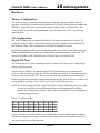
1
User’s Manual
Flashlite 386Ex
Flashlite 386Ex User’s Manual
JK microsystems
Unless otherwise noted, this document and the information herein disclosed are proprietary to
JK microsystems, Inc. Any person or entity to whom this document is furnished or having
possession thereof, by acceptance, assumes custody thereof and agrees that the document is given
in confidence and will not be copied or reproduced in whole or in part to meet the purposes for
which it was delivered.
The information in this document is subject to change without notice, and should not be
construed as a commitment by JK microsystems, Inc. JK microsystems, Inc. will make every
effort to inform users of substantive errors.
JK microsystems, Inc. disclaims all liability for any loss or damage resulting from the use of this
manual or any software described herein, including without limitation contingent, special, or
incidental liability.
JK microsystems, Inc. recognizes our customer’s need for a consistent product and will make
every effort to provide one. In order to provide the best possible product for all of our customers,
we reserve the right to make incremental improvements in our product designs.
Flashlite is a trademark of JK microsystems, Inc. MS-DOS is a registered trademark of Microsoft
Corporation. XDOS is a copyright of HBS Corporation. All other brand and product names are
trademarks or registered trademarks of their respective companies.
Flashlite 386Ex User’s Manual Version 3.1
Copyright © JK microsystems, Inc.
All rights reserved
Printed in U.S.A.
Document Part No. 94-0004
Published February 2003
i
JK microsystems
Flashlite 386Ex User’s Manual
Limited Warranty
JK microsystems, Inc. warrants each Flashlite 386Ex to be free from defects in material and
workmanship for a period of 90 days from the date of purchase. This warranty shall not apply to
any unit which has been subject to misuse, neglect, accident, or abnormal conditions of operation.
JK microsystems’ obligation under this warranty is limited to repairing or replacing, at
JK microsystems’ option, any unit returned to the factory within 90 days of the date of purchase,
provided that JK microsystems determines that the unit is defective and has been used in
compliance with the terms of this warranty. If the failure has been caused by misuse, neglect,
accident, or abnormal conditions of operation, repairs will be billed at a nominal cost.
The foregoing warranty is exclusive and in lieu of all other warranties, expressed or implied,
including, but not limited to, any warranty of merchantability or fitness for any particular
purpose. JK microsystems shall not be liable for any special, incidental or consequential
damages, whether in contract, tort, or otherwise.
Important Notice
Life Support / Mission Critical Applications
This product is not fault-tolerant and is not designed, manufactured or intended for use or resale
as on-line control equipment in hazardous environments requiring fail-safe performance, such as
in the operation of nuclear facilities, aircraft navigation or communication systems, air traffic
control, direct life support machines, or weapons systems, in which the failure of our hardware or
software could lead directly to death, personal injury, or severe physical or environmental
damage.
ii
Limited Warranty
Flashlite 386Ex User’s Manual
JK microsystems
Table of Contents
Limited Warranty ............................................................................................................................ ii
Table of Contents ........................................................................................................................... iii
Overview ........................................................................................................................................ 1
Features ........................................................................................................................................... 1
Operation ........................................................................................................................................ 2
Getting Started ................................................................................................................................ 3
Hardware......................................................................................................................................... 5
Memory Configuration ............................................................................................................. 5
I/O Configuration ...................................................................................................................... 5
Digital I/O Ports ........................................................................................................................ 5
Asynchronous Serial (COM) Ports ........................................................................................... 8
RS-485 Configuration ............................................................................................................... 9
Watchdog Circuitry ................................................................................................................... 9
DiskOnChip ............................................................................................................................ 10
Jumpers ................................................................................................................................... 11
JP1 - Not Used .................................................................................................................. 11
JP2 - Hardware Watchdog Enable .................................................................................... 11
JP3 - Watchdog Non-Maskable Interrupt (NMI) Enable .................................................. 11
JP4 - Not Used .................................................................................................................. 11
JP5 - Power Fail Detect .................................................................................................... 11
JP6/JP12 - Boot Location ................................................................................................. 11
JP7 - PLC Bus Vcc ........................................................................................................... 11
JP8 - SRAM Power Select ................................................................................................ 11
JP9 - Socket Memory Type ............................................................................................... 11
JP10 - Bus IRQ 3/5 Select ............................................................................................... 12
JP11 - Bus IRQ 4/6 Select ............................................................................................... 12
JP13 - PLC Bus Power ..................................................................................................... 12
Cables and Connectors ........................................................................................................... 12
Software ........................................................................................................................................ 15
Supported PC BIOS Functions ............................................................................................... 15
Interrupts ................................................................................................................................. 15
Utilities ......................................................................................................................................... 17
UP.COM ................................................................................................................................. 17
DOWN.COM .......................................................................................................................... 17
FORMAT.COM ...................................................................................................................... 18
EDIT.COM ............................................................................................................................. 18
DOS .............................................................................................................................................. 19
XDOS Command Reference ................................................................................................... 19
QuickBASIC Console I/O ............................................................................................................ 22
Specifications ................................................................................................................................ 23
Contact Information ...................................................................................................................... 25
Table of Contents
iii
JK microsystems
iv
Flashlite 386Ex User’s Manual
Flashlite 386Ex User’s Manual
JK microsystems
Overview
The Flashlite 386Ex single board computer is based on the Intel 386Ex microcomputer. The
386Ex is a high performance, 32-bit, single-chip microcomputer that is software compatible with
the Intel 80386 family of microprocessors. DOS compatibility allows development in a familiar
environment with a wide range of tools. High endurance flash memory eliminates EPROM
programming without worry of damaging the onboard non-volatile memory with repeated
program cycles. Applications are uploaded directly into the flash disk. Expansion options
provide high capacity flash storage eliminating the size and reliability problems associated with
electro-mechanical storage devices.
Software development for the Flashlite is remarkably simple and quick. Programs are written on
a PC compatible computer in the language of your choice. After your application has been
compiled or assembled and linked into .EXE or .COM form, it is uploaded to the Flashlite’s flash
disk with your favorite telecommunications program using the X-Modem protocol. The
application can then be tested and debugged through the console serial port. When the application
is running to your satisfaction, the startup batch file can be modified so that the application will
load and execute upon reset or powerup.
Features
25MHz Intel 386Ex Processor
256k / 512k Bytes SRAM Memory
512k Bytes Flash Memory
High Speed PC Compatible Serial Ports:
1 Full-Function (8-wire) RS-232 Port
1 Software Configurable as 3-wire RS-232 or RS-485
Synchronous 4-Wire Serial Port
3 PC Compatible Counter/Timers
Hardware Watchdog
36 Digital I/O Lines
2 Enhanced DMA Channels
Clock Calendar
32Pin Dip Socket to accept 512k x 8 bit SRAM, 512k x 8 bit Flash, or M-Systems
DiskOnChip 2000.
High-Efficiency Switching Power Supply (7-34V DC Input)
Full Address/Data Expansion Bus
Overview
1
JK microsystems
Flashlite 386Ex User’s Manual
Operation
The Flashlite 386Ex is configured with two ‘disk drives’ A: and B:. Drive A: contains the
operating system, the BIOS, and utility programs essential to the operation of the Flashlite. Drive
A: is read-only. Drive B: is read/write and contains optional utility programs and is available for
user files and applications.
The serial port commonly known as COM2 on the PC is the console for the Flashlite. The port is
configured for 9600 baud, 8 data bits, 1 stop bit and no parity. This is the primary mode of
communicating with the Flashlite. DOS and the BIOS treat the console port as the logical devices
STDIN and STDOUT. The second port is addressed and assigned interrupt vectors the same as
COM1 on a PC.
When power is applied to the Flashlite or when it is reset, the board goes through its initialization
procedure and then starts DOS. A simple AUTOEXEC.BAT file is executed and then the board is
ready to use. The batch file performs several functions before the user is given control. The DOS
search path is set, the DOS prompt is set, the CNTL-C flag (discussed later in this manual) is
checked and finally, an attempt is made to execute a file named STARTUP on the B: drive. This
provides a convenient way for custom applications to execute immediately after initialization of
the Flashlite. If you wish to have your application start automatically, create a batch file named
STARTUP.BAT that invokes the program. It is possible, but not recommended, to rename your
application STARTUP.EXE or STARTUP.COM. If this is done and the program locks up, typing
CNTL-C at bootup may not break the program and exit to the DOS prompt.
!
2
Although the flash memory devices used have a guaranteed lifetime of over 10,000 write
cycles, it is possible for an application to quickly wear them out. The flash memory is
intended to store programs and setup data which are normally not changed. Avoid storing
data or frequently changed information on the flash disk.
Operation
Flashlite 386Ex User’s Manual
JK microsystems
Getting Started
To begin development with the Flashlite, you will need a PC compatible computer with a
telecommunications program and a free serial port. Connect the Flashlite’s connector J11 to the
PC’s serial port with a 9-pin ribbon cable, PN 86-0000. Run the telecommunications program and
configure the serial port for 9600 baud, 8 data bits, 1 stop bit and no parity. Hardware and
Software Handshaking are not required. Apply power to the Flashlite, using our A/C adapter PN
88-0005 or a source of unregulated DC between 7 and 34 volts, capable of supplying 2 Watts. J1
pin 1 or J4 pin 1 (square pad on bottom of board) is positive.
The Flashlite should respond with a welcome message and a B: prompt. Enter DIR to look at the
directory of drive B:. If you do not get a welcome message or characters that you type do not
echo, you need to check your serial port setup. To test everything but the Flashlite, remove the
serial cable from J11 and jumper pins 3 and 5 with a wire or paper clip. If characters typed on the
keyboard are not echoed on the screen, the problem is with your setup. You must resolve the
problem before you can continue.
If you were able to do a DIR, take a few minutes to explore the contents of the Flashlite’s file
system. You will find all of the essential utilities on drive A: and some optional programs on
drive B:. Drive A: is write-protected and cannot be altered. Drive B: is read/write and can be
changed or reformatted.
After you have looked at the programs on the Flashlite, the next step is to try to upload a file.
This is the procedure for getting a file from your PC to the Flashlite. On the Flashlite, type the
command UP followed by the name of the file you wish to upload. The Flashlite will begin
sending characters to your PC polling it for the file.
On your PC, start the transfer, usually by pressing the PgUp key. The telecomm program should
respond by requesting the file name and protocol. Enter the file name and select X-Modem for
the protocol. The transfer should start and when it is complete, you should get a new B: prompt
on the screen. If the transfer does not work, the problem is most likely the Carrier Detect signal
(pin 1 on the DB-9 connector) into the PC being sensed as low or false. Make sure that the signal
is at least +3 volts into your PC if you are not able to transfer files.
If the transfer terminated without problems, you have a working development environment for
the Flashlite controller. At this point, you may wish to download the files EDIT.COM and
BASIC.COM from the Flashlite to your PC. Start the download on the Flashlite by typing DOWN
BASIC.COM and pressing Enter. On your PC, begin the transfer, usually by pressing PgDn.
After the file is transferred, repeat the process with EDIT.COM. These files are also found on the
JK microsystems web site.
Getting Started
3
JK microsystems
Flashlite 386Ex User’s Manual
The Flashlite has a hardware clock calendar. Time and date can be set with the following
commands:
B:\>TIME 13:30:00 Sets the time to 1:30 pm
B:\>DATE 11-19-99 Sets the date to November 19, 1999
When power is applied to the Flashlite, one of the first things the BIOS initialization code does is
check for a CNTL-C character typed at the console. If this character is typed as soon as the board
is powered up or reset, a flag is set which overrides the quiet state of the console (discussed
below). When DOS runs its AUTOEXEC.BAT file on drive A:, the state of the CNTL-C flag is
also checked and any user application set to run on drive B: is not loaded. This insures that a
hung application or quiet console can always be interrupted.
If the CNTL-C flag is not set, the AUTOEXEC file will attempt to transfer control to a file named
STARTUP on drive B:. DOS also looks for and, if present, loads CONFIG.SYS from drive B:.
The Flashlite console output and input can be controlled using the QUIET and NOQUIET
commands. This is useful for applications where both serial ports must talk to hardware devices
without disturbance from console messages.
Running QUIET will turn off both input and output on the console port, allowing applications to
use it as COM2. Pressing CNTL-C immediately after reset or powerup will restore the console
until the next reboot. Running NOQUIET will restore the default setting of an active console.
QUIET modifies a byte in the BIOS Flash data area and will take effect after the board is reset. If
you need to toggle the state of the console while an application is running, a one can be written to
the byte at 40:8B (BIOS RAM Data) to disable the console or a zero can be written to enable the
console. Changes to the quiet flag stored in RAM will not change the state of the flag in Flash
and may not be valid after a reset.
!
4
A Flashlite in quiet mode may appear to be non-functional. When troubleshooting a
system, always try pressing CNTL-C while applying power.
Getting Started
JK microsystems
Flashlite 386Ex User’s Manual
Hardware
Memory Configuration
The 386Ex processor is initially configured in real mode with a physical address space of 1
megabyte. The SRAM is located between 00000h and 7FFFFh, the flash is between 80000h and
FFFFFh. A 32-pin DIP socket is provided for additional flash, RAM, or EPROM data. This
memory can be accessed by reprogramming the chip select unit in the 386Ex or by entering
protected mode.
I/O Configuration
The 386Ex is configured for enhanced DOS mode. This mode provides access to the PC/AT
peripherals such as UARTs, counter/timers, and the interrupt controller at their traditional I/O
port addresses. Other 386Ex peripherals are accessible in expanded I/O space.
For addressing and programming the peripherals specific to the 386Ex, please refer to the Intel
386Ex Embedded Microprocessor User’s Manual (Intel document number 272485-002). The
manual is available in PDF format from our web site at http://www.jkmicro.com
Digital I/O Ports
The Flashlite has six I/O ports controlling a total of 36 bits of I/O. The ports are configured in
groups as described below.
Signals on Ports A,B and C are generated by an 82C55 general purpose programmable I/O
device. A word of caution, any time the 82C55 control register is written to, any output bit that is
in the ON state will be turned OFF. This is a feature of the silicon aimed at protecting outputs
from driving unknown loads that could possibly damage the chip. Ports D and E are generated by
a programmable logic chip. Ports F and G are I/O pins on the 386Ex processor.
NOTE:Be careful to change only the required bits when working with the I/O ports. Some pins
are used to control other on-board functions that can be reprogrammed or disabled
through these configuration registers. Refer to the chip datasheets for more information
on configuring these ports.
Port A, I/O Address 60 Hex
Bit
Name
Default
Pin
7
6
5
4
3
2
1
0
PA.7
PA.6
PA.5
PA.4
PA.3
PA.2
PA.1
PA.0
IN
IN
IN
IN
IN
IN
IN
IN
J2-11
J2-13
J2-15
J2-17
J2-19
J2-21
J2-23
J2-25
Port A is located at I/O address 60 hex and is configured as a group as either inputs or outputs.
The default configuration is inputs. To make all bits output, set bit 4 of I/O address 63 hex to a
zero, preserving the state of the other bits.
Hardware
5
JK microsystems
Flashlite 386Ex User’s Manual
Port B, I/O Address 61 Hex
Bit
7
6
5
4
3
2
1
0
Name
PB.7
PB.6
PB.5
PB.4
PB.3
PB.2
PB.1
PB.0
Default
OUT
OUT
OUT
OUT
OUT
OUT
OUT
OUT
Pin
J2-12
J2-14
J2-16
J2-18
J2-20
J2-22
J2-24
J2-26
Port B is located at I/O address 61 hex and is configured as a group of either inputs or outputs.
The default configuration is outputs. To make all bits input, set bit 1 of I/O address 63 hex to a
one, preserving the state of the other bits.
Note: PB.1 is used to gate the PC speaker output. The speaker output may not be used when
PB.1 is controlled by the user program.
Port C, I/O Address 62 Hex
Bit
7
6
5
4
3
2
1
0
Name
PC.7
Default
OUT
PC.6
PC.5
PC.4
PC.3
PC.2
PC.1
PC.0
OUT
OUT
OUT
IN
IN
IN
IN
Pin
J14-5
J14-7
J14-9
J14-11
J14-18
J14-17
J14-20
J14-19
Port C is located at I/O address 62 hex and is configured as 2 groups of 4 bits each. The default
configuration for bits PC.0 to PC.3 is inputs. To make these bits outputs, set bit 0 of I/O address
63 hex to a zero.
The default configuration for bits PC.4 to PC.7 is outputs. To make these bits inputs, set bit 3 of
I/O address 63 hex to a one. When reconfiguring the I/O status of these pins, be sure to preserve
the state of the other bits.
Port D, I/O address FA02 hex
Bit
7
6
5
4
3
2
1
0
Name
-
-
-
-
PD.3
PD.2
PD.1
PD.0
Default
-
-
-
-
IN
IN
IN
IN
Pin
-
-
-
-
J7-4
J7-3
J7-2
J7-1
Port D is located at I/O address FA02 hex and is configured as a group as either input or output.
The default configuration of Port D is input. To configure Port D as outputs, set bit 0 of I/O
address FA00 hex to a one.
Port E, I/O Address FA03 Hex
Bit
7
6
5
4
3
2
1
0
Name
-
-
-
-
PE.3
PE.2
PE.1
PE.0
Default
-
-
-
-
IN
IN
IN
IN
Pin
-
-
-
-
J7-8
J7-7
J7-6
J7-5
6
Hardware
JK microsystems
Flashlite 386Ex User’s Manual
Port E is located at I/O address FA03 hex and is configured in three groups. The default
configuration is input. To configure PE.0 and PE.1 as output, set bit 1 of I/O address FA00 to a
one. To configure PE.2 as an output, set bit 2 of I/O address FA00 to a one. To configure PE.3 as
an output, set bit 3 of I/O address FA00 to a one. In each case, be sure to preserve the other bit
settings.
Port F, I/O Address F860 and F862 Hex
Bit
Name
Default
Pin
7
6
5
4
3
2
1
0
PF.7
PF.6
PF.5
PF.4
-
-
-
-
IN
IN
IN
IN
-
-
-
-
J12-4
J12-3
J12-2
J12-1
-
-
-
-
The data on Port F can be read by inputting I/O address F860 hex. The default configuration is
input. Each bit of Port F can be individually configured for input or output. To configure a bit for
output, write a zero in that bit position to I/O address F864 hex. To output data on Port F, write
the data to address F862 hex.
P1PIN:
P1LTC:
P1DIR:
F860h, Port Pin Status Register (read only), bits 4-7
F862h, Port Latch Register, bits 4-7
F864h, Port Direction Register, bits 4-7, 0 for output, 1 for input or open drain
output.
F820h, Port Configuration Register, bits 4-7 low, route P1.4-P1.7 to chip pins
(BIOS Default)
P1CFG:
Port G, I/O Address F870 and F872 Hex
Bit
7
6
5
4
3
2
1
0
PG.5
PG.4
IRQ6
PG.3
IRQ5
PG.2
PG.1
IRQ3
PG.0
IRQ4
Name
-
-
Default
-
-
IN
IN
OUT
IN
IN
IN
Pin
-
-
J10.8
J12-8
J12.7
J10.19
J13.15
J13.17
EXFLAG
PCFLAG
The data on Port 3 can be read from I/O address F870 hex. The default pin direction is shown
above. Each bit of Port 3 can be individually configured as an input or output. To configure a bit
as an output, write a zero to that bit position in I/O address F874 hex. To output data on Port 3,
write the data to I/O address F872 hex. When used as inputs, these pins can also be configured to
generate processor interrupts.
P3PIN:
P3LTC:
P3DIR:
P3CFG:
F870h, Port Pin Status Register (read only), bits 0-5
F872h, Port Latch Register, bits 0-5
F874h, Port Direction Register, bits 0-5, 0 for output, 1 for input or open drain
output.
F824h, Port Configuration Register, bits 0-5 low, route P3.0-P3.5 to chip pins.
Hardware
7
JK microsystems
Flashlite 386Ex User’s Manual
Asynchronous Serial (COM) Ports
The Flashlite has 2 serial ports, COM1 and COM2. Both ports are internal to the 386Ex and are
compatible with the UARTs on a PC and the National Semiconductor 16C450 UART. The
maximum data rate is 115k Baud.
COM1 is wired as Data Terminal Equipment (DTE) for connection to a peripheral such as a
modem. This is a full function RS-232 port implementing all of the handshaking and control
lines with the exception of the Ring Indicator input. See Table 2k for the connector wiring. The
UART base address is at I/O location 3F8h and can be configured to use IRQ 4.
COM2 is the default console and is wired as Data Communications Equipment (DCE) for direct
connection to a computer or terminal. This port is software configurable as a 3 wire RS-232 port
implementing RxD and TxD or as a half duplex RS-485 port. See Table 2l for the connector
wiring. The UART base address is at I/O location 2F8h and can be configured to use IRQ 3.
The following table shows the UART configuration and control registers. Please refer to the Intel
386Ex data sheet for more information on the serial ports and their configuration.
7
Base
6
5
4
3
2
1
0
Receive/Transmit Holding Register / Divisor Latch Low (DATA)
Data In, Data Out
Base+1
Interrupt Enable Register (IER)
0
Base+2
0
0
0
Modem
Status
Receive Line
Transmit
Status
Buffer Empty
Reserved
Interrupt Source:
00=Modem Status
01=Transmit Buffer Empty
10=Receive Buffer Full
11=Receiver Line Status
Interrupt Identification Register / Divisor Latch High (IIR)
Reserved
Reserved
Reserved
Reserved
Base+3
Line Control Register (LCR)
Base+4
Divisor
Send Break Parity:
Latch
000=None, 001= Odd, 011=Even,
Access
101=Mark, 111=Space
Modem Control Register (MCR)
0
Base+5
0
0
Transmit
Transmit
Register
Buffer Empty
Empty
Modem Status Register (MSR)
DCD
Word Length:
00=5, 01=6,
10=7, 11=8
Loop Back
Test
Ext. Int.
Enable
Out1
RTS
DTR
Break
Interrupt
Framing
Error
Parity Error
Overrun
Error
Receive
Buffer Full
RI
DSR
CTS
D
DCD
D
RI
D
DSR
D
CTS
Table 1: UART Registers
8
Stop Bits:
0=1, 1=2
Interrupt
Pending
(0=Pending)
Line Status Register (LSR)
Reserved
Base+6
Receive
Buffer Full
Hardware
Flashlite 386Ex User’s Manual
JK microsystems
The DATA and IER registers also hold the baud rate divisor. When the high bit of the LCR
(DLA) is set, the divisor value can be written to DATA and IER. DATA contains the low byte and
IER contains the high byte. To determine the required divisor, divide 115200 by the required
baud rate. Program the divisor with the nearest integer value. When access to the divisor value
is no longer required, clear the DLA bit.
RS-485 Configuration
The COM2 port of the Flashlite can be configured and used for RS-485 communications. In
order to avoid conflicts with DOS and the BIOS, it is first necessary to move the console to
COM1. This is done using the utility program CON2COM1. Please note that COM1 (J6) is
pinned out as DTE and you must use a null modem cable to connect it to a PC serial port.
To enable RS-485 operation (and disable RS-232) on COM2, clear bit 6 of I/O port F872 hex.
#define EN485_MASK 0xBF
#define EN485_REG 0xF872
outportb(EN485_REG, (inportb(EN485_REG) & EN485_MASK) ); // change to RS-485
Bit 0 of the PINCFG register must be set to allow control of the RS-485 transmit enable pin. The
PINCFG register is located at I/O port F826 hex.
#define PINCFG 0xF826
outportb(PINCFG, (inportb(PINCFG) | 0x01) ); // connect TE to chip pkg
The RTS line on COM2 is used to control the RS-485 transmitter. To transmit RS-485 data, set
bit 1 of I/O port 2FC hex (mirrored at F8FC hex). To receive RS-485 data, clear bit 1. Note that
the state of the chip pin is the inverse of the bit in the register (register=1, pin=0).
#define TX_MASK 0x02
#define TX_MASK_REG 0xF8FC
outportb(TX_MASK_REG, (inportb(TX_MASK_REG) | TX_MASK) ); // enable tx
outportb(TX_MASK_REG, (inportb(TX_MASK_REG) & ~TX_MASK) ); // disable tx
Two utility programs are available to aid RS-485 development. 485RX accepts RS-485 data and
displays it on the console. 485TX accepts console data and sends it out the RS-485 port. The
console must be switched to COM1 when using the utilities. These programs are installed on
drive A:.
Watchdog Circuitry
The Flashlite has two Watchdog protection features. The Hardware Watchdog is part of the reset
control chip and the Watchdog Timer is a feature of the 386Ex processor chip.
The Hardware Watchdog requires that software write to a specific I/O port before its timer
expires. If the timer expires, a system wide reset is issued and the board will restart. This is the
preferred watchdog due to its ability to generate a hardware reset. JP2 must be installed to enable
the Hardware Watchdog.
The BIOS will reset the Hardware Watchdog for approximately 5 seconds after power up giving
the user application enough time to load. The user application must write a 0C hex to I/O
location FF04 hex at least once every 1.6 seconds.
Hardware
9
JK microsystems
Flashlite 386Ex User’s Manual
The Watchdog Timer is a counter that decrements once per processor clock cycle. When the
counter reaches zero, the WDTOUT pin is asserted for 8 processor clock cycles. This signal can
be internally routed to IR7 or externally jumpered to generate a Non-Maskable Interrupt (NMI).
Software should periodically reload the counter register indicating that it is behaving properly.
The watchdog timer system has three modes: General Purpose, Software, and Bus Monitor. In
General Purpose mode the counter can only be reloaded after it times out. This makes it difficult
to use for system protection. The Software mode allows the countdown register to be reloaded
before it times out. This allows protection against locked up software. The Bus Monitor mode is
not applicable to the Flashlite hardware.
To enable the watchdog in Software mode, use the following sequence:
1.
2.
3.
Write the upper byte of the reload value to the WDTRLDH register (F4C0h).
Write the lower byte of the reload value to the WDTRLDL register (F4C2h).
Write two sequential words, F01Eh followed by 0FE1h, to the WDTCLR register (F4C8h).
Software will periodically repeat this sequence to refresh the counter and prevent it from
generating an interrupt. The current value of the counter can be read from WDTCNTH and
WDCNTL at F4C4h and F4C6h. Once enabled in Software mode, the timer can not be disabled.
The watchdog is active on power up, defaults to general purpose mode and the counter has an
initial value of 3FFFFF hex. The counter can be disabled by setting bit zero of the WDTEN
register at F4CAh. The Watchdog output is normally disabled by jumper JP3. If the watchdog is
required, JP1 pins 1 and 2 should be shorted. Please refer to the Intel 386EX Embedded
Microprocessor User’s Manual for more information.
DiskOnChip
M-Systems’ DiskOnChip is a new generation of high performance single-chip Flash Disk. The
DiskOnChip has become the standard Flash Disk module for Embedded Single Board
Computers. The DiskOnChip MD2000 is a Flash Disk in a standard 32-pin DIP package that has
built-in TrueFFS (True Flash File System) technology, allowing full read/write disk emulation.
TrueFFS provides hard disk compatibility at both the sector and file level. Drives larger than
32Mbytes will require partitioning for use with XDOS.
DiskOnChip expansion is only supported on the Flashlite with 512K RAM / 512K Flash. Install
the DiskOnChip module in the memory expansion socket U1. Note the location of pin 1. Set the
memory type jumper (JP9) for Flash memory. If the DiskOnChip is installed and functioning,
there will be an installation message that is displayed during the boot process and a C: drive will
be available to DOS.
Bios Version 3.2g for Flashlite 386Ex with 256k or 512k Ram
DOC Socket Services - Version 0.2
(C) Copyright 1992-1996, M-Systems Ltd.
TrueFFS-BIOS -- Version 3.3.7 for DiskOnChip 2000 (V1.10)
Copyright (C) M-Systems, 1992-1998
DOS Version 3.3c for JK microsystems Flashlite
(C) HBS Corp and JK microsystems 1991-1999
B:\>
10
Hardware
Flashlite 386Ex User’s Manual
JK microsystems
Jumpers
JP1 - Not Used
This jumper jumper is not used.
Default position: Open, no jumper fitted.
JP2 - Hardware Watchdog Enable
This jumper enables the Hardware Watchdog. If the Hardware Watchdog is required, JP2 pins 1
and 2 should be shorted.
Default position: Open, Hardware Watchdog disabled.
JP3 - Watchdog Non-Maskable Interrupt (NMI) Enable
This jumper connects the 386Ex watchdog signal to the processor NMI. If the watchdog is
required, JP1 pins 1 and 2 should be shorted.
Default position: 2-3, Watchdog NMI disabled.
JP4 - Not Used
This jumper is not used.
Default position: Open, no jumper fitted.
JP5 - Power Fail Detect
This jumper connects the power fail detection circuitry to Port B pin 3. When this jumper is
installed, Port B pin 3 will be driven high when the raw DC input voltage to the board is less than
8 volts.
Default position: Open, no jumper fitted.
JP6/JP12 - Boot Location
These jumpers allows the board to boot from the expansion socket. This is useful when
performing field updates of the on-board Flash memory or when using an operating system other
than DOS. Short JP6 pins 1-2 and JP12 pins 2-3 to boot from the on-board memory or jumper
JP6 pins 2-3 and JP12 pins 1-2 to boot from the expansion socket.
Default position: JP6 pins 1-2 and JP12 pins 2-3, Boot from on-board flash.
JP7 - PLC Bus Vcc
This jumper connects Vcc to the PLC Bus (J14) connector when installed.
Default position: 1-2, Vcc available on PLC Bus (J14).
JP8 - SRAM Power Select
This jumper allows the SRAM contents to be maintained by the on-board battery when power
fails. Jumper pins 1-2 for battery backup, pins 2-3 for Vcc power.
Default position: 2-3, SRAM does not have battery backup.
JP9 - Socket Memory Type
These jumpers configure the memory type to be used in the expansion socket. Jumper pins 1-2
and 3-4 when using Flash or DiskOnChip, jumper 2-3 and 4-5 when using SRAM.
Default position: 1-2 and 3-4, Flash installed in expansion socket.
Hardware
11
JK microsystems
Flashlite 386Ex User’s Manual
JP10 - Bus IRQ 3/5 Select
This jumper selects which IRQ is available on J13 pin 15. Jumper pins 1-2 to select IRQ5,
jumper pins 2-3 to select IRQ3.
Default position: 1-2, IRQ5 on Extended Bus.
JP11 - Bus IRQ 4/6 Select
This jumper selects which IRQ is available on J13 pin 17. Jumper pins 1-2 to select IRQ6,
jumper pins 2-3 to select IRQ4.
Default position: 1-2, IRQ6 on Extended Bus.
JP13 - PLC Bus Power
This jumper allows unregulated input power to be routed to the PLC Bus (J14, pin 4). Install this
jumper to route power to the bus.
Default position: Open, Raw power not connected to PLC Bus.
Cables and Connectors
The following tables show the connector pin and signal name for each pin. For some pins, the
signal direction is also shown.
NOTE:N/C indicates no connection and PULLUP indicates a 1k ohm pullup resistor to Vcc.
Outputs refer to signals driven by the board and received by a peripheral. Inputs are
driven by a peripheral and received by the board.
Pin 1 of a connector can be identified in several ways. Pin one has a square PCB pad and the
others are round. This should be visible on the bottom of the PCB. Pin one will also be
identified on the board silkscreen with a ‘1’ and/or a dot. Dual row headers have ODD numbered
pins on one side and EVEN numbered pins on the other. The dual row header numbering scheme
follows the numbering of an IDC style ribbon cable. This numbering may not be identical to
connectors with discrete wires. Use caution when connecting cables to the Flashlite.
J1
Power
J4
Power
7-34 VDC
1
7-34 VDC
1
RESET/
2
GN D
2
GN D
3
Table 2b: Power Pinout
Table 2a: Power Pinout
J3
Speaker
RS-485
SPK R
1
DATA +
1
AUX
2
GN D
2
GN D
3
DATA -
3
VC C
4
Table 2d: RS-485 Pinout
Table 2c: Speaker Pinout
12
J5
Hardware
JK microsystems
Flashlite 386Ex User’s Manual
J2
P o rt A & B
J1 4
P o rt C / P L C B us
GN D
1
2
VCC
GN D
1
2
VCC
GN D
3
4
VCC
N /C
3
4
D C IN
GN D
5
6
S TX C LK /
P C .7 (S TB /)
5
6
GN D
GN D
7
8
S R X C LK /
P C .6 (A 3 )
7
8
GN D
S S IO R X /
9
10
S S IO TX /
P C .5 (A 2 )
9
10
GN D
PA .7
11
12
P B .7
P C .4 (A 1 )
11
12
GN D
PA .6
13
14
P B .6
P D .2 (D 6 )
13
14
P D .3 (D 7 )
PA .5
15
16
P B .5
P D .0 (D 4 )
15
16
P D .1 (D 5 )
PA .4
17
18
P B .4
P C .2 (D 2 )
17
18
P C .3 (D 3 )
PA .3
19
20
P B .3
P C .0 (D 0 )
19
20
P C .1 (D 1 )
PA .2
21
22
P B .2
P E.2 (W R /)
21
22
P E.3 (LC D )
PA .1
23
24
P B .1
P E.1 (R D /)
23
24
P E.0 (A 0 )
PA .0
25
26
P B .0
VCC
25
26
GN D
Table 2e: Port A & B Pinout
J7
Table 2f: Port C Pinout
P o rt D & E
J1 2
P o rt F
P D .0
1
2
P D .1
P F.4
1
P D .2
3
4
P D .3
P F.5
2
P E.0
5
6
P E.1
P F.6
3
P E.2
7
8
P E.3
P F.7
4
GN D
9
10
VCC
GN D
5
VC C
6
IR Q 5
7
IR Q 6
8
Table 2g: Port D & E Pinout
J1 0
H o st P aralle l P o rt
S TR O B E/
1
2
A U TO /
D7
3
4
ER R O R /
D6
5
6
N /C
D5
7
8
S LC T IN /
D4
9
10
GN D
D3
11
12
GN D
J8
D2
13
14
GN D
RD /
1
2
TA P IN
D1
15
16
GN D
W R/
3
4
TA P O U T
D0
17
18
GN D
P U LLU P 3
5
6
TA P C LK
ACK /
19
20
GN D
C S1/
7
8
TA P M O D E
BU S Y/
21
22
GN D
C S0/
9
10
R ES E T/
P E/
23
24
GN D
UCS/
11
12
GN D
S LC T
25
26
GN D
Table 2h: Port F Pinout
JTA G
Table 2j: JTAG Pinout
Table 2i: Host Parallel Pinout
Hardware
13
JK microsystems
Flashlite 386Ex User’s Manual
COM1 is configured as a DTE port, and is generally used to communicate with a peripheral
device. COM2 is configured as a DCE port, generally being used to connect the Flashlite to
another computer. A 10 pin dual row header to 9 pin to D-type connector may be required to
connect the Flashlite to a peripheral or computer. See the tables below for connector pinouts.
J6
C O M1:
J11
DCD (in)
1
2
DSR (in)
PULLUP
1
2
N /C
RxD (in)
3
4
RTS (out)
TxD (out)
3
4
PULLUP
TxD (out)
5
6
C TS (in)
RxD (in)
5
6
PULLUP
DTR (out)
7
8
N /C
N /C
7
8
PULLUP
GN D
9
10
N /C
GN D
9
10
N /C
Table 2k: COM1 Pinout
J9
Table 2l: COM2/Console Pinout
Processor Bus
GN D
1
2
VCC
J13
GN D
3
4
VCC
GN D
1
2
IRQ 9
MREQ /
5
6
D7
LBA/
3
4
D15
MSTB/
7
8
D6
BS8/
5
6
D14
IO STB/
9
10
D5
IO /
7
8
D13
RW/
11
12
D4
W-R/
9
10
D12
REFRQ /
13
14
D3
D-C /
11
12
D11
RESET/
15
16
D2
ADS/
13
14
D10
IO RD/
17
18
D1
IRQ 3/5
15
16
D9
IO WR/
19
20
D0
IRQ 4/6
17
18
D8
A9
21
22
A19
A24
19
20
A23
A8
23
24
A18
A22
21
22
A21
A7
25
26
A17
A20
23
24
A19
A6
27
28
A16
VCLK
25
26
GN D
A5
29
30
A15
Extended Bus
A4
31
32
A14
A3
33
34
A13
A2
35
36
A12
A1
37
38
A11
A0
39
40
A10
Table 2n: Extended Bus Pinout
Table 2m: Processor Bus Pinout
14
C O M2:
Hardware
Flashlite 386Ex User’s Manual
JK microsystems
Software
Supported PC BIOS Functions
The Flashlite BIOS supports the following functions (software interrupts) common to PC
compatible computers. Please refer to a DOS/PC reference for more information on DOS and
BIOS software interrupts.
Int 10h, Video Driver, Functions 9 and Eh
Int 11h, Get Equipment Configuration
Int 12h, Get Memory Size
Int 13h, Disk Driver, Functions 0-4
Int 14h, Serial Port Driver, Functions 0-3
Int 16h, Keyboard Driver, Functions 0 and 1
Int 19h, Boot System
Int 1Ch, Hook Timer Tick Interrupt
IRQ0 / Int 8, Timer Tick Interrupt
Interrupts
Working with interrupts within the PC architecture can be a bit confusing. The following
information should clarify some of the issues, but it is not a substitute for a detailed DOS/PC
programming reference.
The PC architecture has a 1Kbyte Interrupt Vector Table located at 0000:0000. This table holds
the 4byte address of each Interrupt Service Routine (ISR) providing a total of 256 interrupts.
Most of the interrupts are software interrupts. Software interrupts provide essential services in a
‘known’ location. Hardware interrupt requests have an associated interrupt number and ISR in
the vector table. Refer to a DOS/PC reference for more information on software interrupts.
The numbering of hardware interrupts is the largest point of confusion when working with
interrupts on the Flashlite. The 386Ex processor interrupt pins are referred to as INTx in the Intel
documentation. PC programmers are familiar with IRQ (Interrupt Request) numbers and the
interrupt numbers also referred to as INT numbers. The correlation of all these numbers is critical
when using interrupts. The table below identifies the IRQ, 386Ex INT number, function on a
standard PC, function on the 386Ex and the interrupt number. You will notice a large gap in
interrupt numbers between IRQ7 and IRQ8. This is due to the implementation of two cascaded
interrupt controllers and the PC legacy. IRQ0-7 are on the first controller, found in the original
PC/XT. IRQ8-15 are on the second controller implemented in the PC/AT. IRQ2 notifies the
system when an IRQ is triggered on the secondary controller. Table entries without a 386Ex INT
listed are not available on the package pins of the 386Ex.
Each Programmable Interrupt Controller (PIC) has several control registers and commands, most
of which are configured by the BIOS and should not require modification in most applications.
The primary PIC is located at I/O address 20 hex and the secondary controller is at I/O address
A0 hex.
Software
15
JK microsystems
Flashlite 386Ex User’s Manual
IRQ
386Ex INT PC Function
IRQ0
System Timer
TCU OUT0
08
Keyboard
P3.2
09
IRQ1
INT0
IRQ2
386Ex Function
Cascade
Int. No. (hex)
0A
IRQ3
INT8
COM2
SIO1 INT
0B
IRQ4
INT9
COM1
SIO0 INT
0C
IRQ5
INT1
P3.3
0D
IRQ6
INT2
Floppy Disk
P3.4
0E
IRQ7
INT3
Parallel Port
P3.5
0F
IRQ8
INT4
Real Time Clock
70
IRQ9
INT5
IRQ2 (redirected)
71
IRQ10
TCU OUT1
72
IRQ11
TCU OUT2
73
IRQ12
INT6
IRQ13
IRQ14
INT7
Mouse
74
Math Coprocessor
75
Hard Disk
76
IRQ15
WDTOUT
77
Table 3: Hardware Interrupts
The first command of interest is the Operation Control Word (OCW). Located at BASE+1, it is
the mask byte for the interrupts in that controller. Masked IRQ’s have a one in the corresponding
bit location, enabled interrupts have a zero. Be sure to only change the mask bits for IRQ’s
handled by your program. For example, to enable IRQ 4:
outportb(0x21,(inportb(0x21) & 0xEF);
The other instruction used is the End Of Interrupt (EOI). This instruction is sent to the
appropriate PIC after an interrupt has been processed. The EOI is instruction 20 hex and is sent to
the BASE address of the controller, for example:
outportb(0x20,0x20);
When servicing an interrupt on the secondary controller (IRQ8-15), it is necessary to send an EOI
to both controllers.
16
Software
Flashlite 386Ex User’s Manual
JK microsystems
Utilities
The Flashlite comes preloaded with several utilities to aid system development. These utilities are
located on drive A: of the Flashlite or the Utilities disk.
UP.COM
This utility facilitates uploading files to the Flashlite via the console port using the X-MODEM
transfer protocol. The utility requires the user to supply the name of the incoming file. Unless
otherwise specified, the file is placed in the active directory of the current drive. Be sure that B: is
the current drive or a write-protect error will occur when UP tries to write to the read-only A:
drive.
B:\>up
Upload file with X-MODEM Protocol
Usage: up file...
Version 2.0 for JK microsystems Flashlite V25 and 386Ex
B:\>up test.exe
Ready, start X-modem upload now,
Press CNTL-C to abort...
CCCC
B:\>
DOWN.COM
This utility facilitates downloading files from the Flashlite via the console port using the XMODEM transfer protocol. The utility requires the user to supply the name of the file to transmit.
B:\>down
Download file with X-MODEM Protocol
Usage: down file...
Version 1.0 for JK microsystems SBC products
B:\>down test.exe
Ready, start X-modem download now,
B:\>
Utilities
17
JK microsystems
Flashlite 386Ex User’s Manual
FORMAT.COM
If it becomes necessary to reformat the B: drive, FORMAT provides this function. CAUTION, all
information on the drive will be lost during the formatting process.
B:\>format
Flashlite FLASH Drive Format Program -Version 3.0
System will reboot after successful format...
Press 1 to initialize Drive B as 418 KB disk
Press ESC to exit with no changes
>1
Flash Drive is now formatted
Rebooting system...
EDIT.COM
A simple line editor is included to allow quick creation and modification of batch files or other
text files. EDIT is similar to Microsoft’s EDLIN provided in earlier versions of MS-DOS. It
allows list, insert, delete, and modify. Upon exit, a backup of the original file is created
(filename.BAK) and the edits are saved. If a backup file with the same name already exists, it is
overwritten. A list of commands and their usage is available by entering ‘h’ at the edit prompt (
>> ). The name of the file to edit must be supplied following the command EDIT on the
command line.
B:\>edit test.bat
FlashLite Line Editor v1.0
Enter h for help
New File: test.bat
>> i
0: @echo Batch file being processed...
1: mytsr
2: myapp
3: ^Z
>> l
0: @echo Batch file being processed...
1: mytsr
->
2: myapp
>> q
Save before exit (Y,n): y
File Saved
B:\>
18
Utilities
JK microsystems
Flashlite 386Ex User’s Manual
DOS
JK microsystems’ controllers use XDOS, a compact operating system for embedded applications.
The XDOS command structure is nearly identical to MS/PC DOS version 3.3. The switches for
the DIR command have been changed and expanded. XDOS does not support redirected input or
output with the use of < and >, but does support pipes ( | ). None of the external DOS commands
are provided due to storage constraints. XDOS does not support installable file system functions.
XDOS Command Reference
In the list below, XDOS commands are followed by a function description and their format
including available parameters and switches. Items in boldface type must be entered. Capitals or
lowercase letters may be used. Items in italics are parameters. Those in boldface italics must be
entered, those in [ ] are optional. All switches are optional. They are shown as [/X]. Spaces and
punctuation are to be included. An ellipsis ... following items means that you may repeat the
items as often as needed. Do not enter the ellipsis or the square brackets. Most XDOS commands
allow the use of wildcards in filenames and extensions. When wildcards (?=one character, *=any
character or characters) are used, the command is executed once for each matching file.
Common parameters are:
[ d:]
drive specification - a letter followed by a colon (:), e.g. A:, if no drive is
specified, the default drive is used.
[path]
the path DOS must take in traveling from one directory to another; directory
names are separated by a backslash (\).
[filename] up to 8 characters used to name a file.
[.ext]
a three character extension may be added to a filename; an extension is
separated from a filename by a period.
CD / CHDIR
Function:
Changes the current directory
Format:
CD or CHDIR [[d:]path]
COPY
Function:
Copies a file, combines two or more files into one file, or transfers data
between files and DOS devices
Format:
COPY [d:][path]filename[.ext][switches]
[+[d:][path]filename[.ext][switches]
[d:][path][filename[.ext]][switches]
Switches:
/V - verify the contents of new file
/A - copy file in ASCII format
/B - copy file in binary format
DOS
19
JK microsystems
Flashlite 386Ex User’s Manual
DATE
Function:
Format:
DEL / ERASE
Function:
Format:
Displays or changes the current DOS date.
DATE [mm-dd-yyyy]
Deletes (erases) one or more files from a disk
DEL or ERASE [d:][path][filename[.ext]]
DIR
Function:
Format:
Switches:
MD / MKDIR
Function:
Format:
Lists directory entries
DIR [d:][path][filename[.ext]][switches]
/a - display file attributes
/b - sort by file size (in bytes)
/d - sort entries by date and time
/f - display entries by alphabetic file name order
/n - display entries in directory order (do not sort)
/s - include system and hidden files in output
/h - display this Help screen (any invalid key)
Creates a subdirectory
MD or MKDIR [d:]path
PATH
Function:
Format:
Specifies directories that DOS is to search when trying to locate executable
files
PATH [[d:]path[;[d:]path ...]]
PROMPT
Function:
Sets the DOS system prompt
Format:
PROMPT [text]
Text:
Resulting Character(s):
$t The current time stored by DOS
$d The current date stored by DOS
$p The current directory
$v The version of DOS being used
$n The default drive
$g The character >
$l The character <
$b The character |
$q The character =
$$ The character $
$_ Carriage return plus line feed
20
DOS
JK microsystems
Flashlite 386Ex User’s Manual
REN
Function:
Format:
RD / RMDIR
Function:
Format:
Renames a file
REN [d:][path]filename[.ext] filename[.ext]
Deletes a subdirectory
RD or RMDIR [d:]path
TIME
Function:
Format:
Displays or changes the current DOS time
TIME [hh:mm:ss.xx]
Function:
Format:
Display the contents of a file
TYPE [d:][path]filename[.ext]
Function:
Format:
Displays the DOS version number
VER
Function:
Format:
Displays the volume label of specified drive
VOL [d:]
TYPE
VER
VOL
DOS
21
JK microsystems
Flashlite 386Ex User’s Manual
QuickBASIC Console I/O
Some of the code produced by Microsoft QuickBASIC and QuickBASIC Professional compilers
does not execute properly on the Flashlite. In the case of console I/O, we believe that
QuickBASIC is generating code for specific hardware and software not present on the Flashlite
controller.
There are two problems with console I/O. The first is that a PRINT statement will not send output
to the console port. To output text to the console, open “cons:” as a file and print to it.
OPEN “o”, 1, “cons:”
PRINT #1, “This is a test of Console output”
The second problem is that an INPUT statement will not echo data entered by the user. To work
around this problem, use the line input function listed below.
rem
rem
rem
rem
linein returns the echoed string of text linein$ from
the console.
If you need the text in the form of a number, use
VAL(linein$) to convert the string to a number
linein:
linein$ = “”
linemore:
a$ = INKEY$
IF a$ = “” THEN GOTO linemore
IF a$ = CHR$(13) THEN GOTO linedone
IF a$ <> CHR$(8) THEN GOTO getchar
PRINT #1, CHR$(8); CHR$(32); CHR$(8);
linein$=left$(linein$,(len(linein$)-1))
GOTO linemore
getchar:
PRINT #1, a$;
linein$ = linein$ + a$
GOTO linemore
linedone:
PRINT #1, “”
RETURN
22
QuickBASIC/PowerBASIC Console I/O
JK microsystems
Flashlite 386Ex User’s Manual
Specifications
Supply Voltage:
Supply Power:
Supply Current:
Operating Temperature:
Humidity:
7 - 34 V DC, unregulated
1.8 Watts (nominal)
260mA @ 7 Volts input
150mA @ 12 Volts input
75mA @ 24 Volts input
-20 to +85 °C
5 - 90 % non-condensing
I/O Port A,B & C Characteristics:
Symbol
VIL
VIH
VOL
VOH
Parameter
Input Low
Input High
Output Low
Output High
MIN
MAX
0.8
Units
V
V
V
V
2.0
0.4
3.0
Condition
IOL= 2.5mA
IOH= -2.5mA
I/O Port D & E Characteristics:
Symbol
VIL
VIH
VOL
VOH
Parameter
Input Low
Input High
Output Low
Output High
MIN
-0.5
2.0
MAX
0.8
Vcc+0.5
0.45
Units
V
V
V
V
MAX
0.8
Vcc+0.3
0.45
Units
V
V
V
V
2.4
Condition
IOL= 12mA
IOH= -4mA
I/O Port F Characteristics:
Symbol
VIL
VIH
VOL
VOH
Parameter
Input Low
Input High
Output Low
Output High
Mating Connectors:
Connector
J6, J7, J11
J2, J10, J14
Pins
J1, J5
J12
Pins
Mechanical:
Dimensions
Weight
Mfg
Molex
Oupiin
Molex
Oupiin
Molex
Oupiin
Molex
Molex
Molex
MIN
-0.3
2.0
Vcc-0.5
Condition
IOL= 8mA
IOH= -8mA
MFG P/N
22-55-2101
4072-2X05H
22-55-2261
4072-2X13H
16-02-0096
404-PIN-10K
22-01-2031
22-01-2081
08-50-0114
JK micro P/N
28-0030
28-0031
28-0033
28-0012
28-0037
28-0013
4.20" x 3.60" (106.7 mm x 94.1 mm)
2.9oz (82.2 gm)
Specifications
23
JK microsystems
24
Flashlite 386Ex User’s Manual
Specifications
Flashlite 386Ex User’s Manual
JK microsystems
Contact Information
JK microsystems, Inc.
Davis, CA 95616
Telephone:
Fax:
Email:
Web:
(530) 297-6073
(530) 297-6074
[email protected]
http://www.jkmicro.com
Intel Corporation
2200 Mission College Blvd.
P. O. Box 58119
Santa Clara, CA 95052
Telephone:
Fax:
BBS:
Web:
(800) 548-4725, (708) 296-9333
(800) 525-3019
(503) 264-7999
http://www.intel.com
M-Systems
DiskOnChip 2000
39899 Balentine Drive, Suite 335
Newark, CA 94560
Telephone:
Fax:
Email:
Web:
(510) 413-5950
(510) 413-5980
[email protected]
http://www.m-sys.com
Dunfield Development Systems
Micro-Basic, Development Tools
P. O. Box 31044
Nepean, Ontario, Canada K2B 8S8
Telephone:
Fax:
BBS:
Email:
Web:
Rev
----3.1
(613) 256-5820
(613) 256-5821
(613) 256-6289
[email protected]
http://www.dunfield.com
Date
--------11Feb03
Author
-------EW
Changes
----------------------------------------------------------Add Change Log, Reformat for web,
revise table 2f (84-0011E assembly)
Contact Information
25