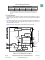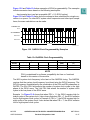
1
SECTION 13
QUEUED ANALOG-TO-DIGITAL CONVERTER MODULE-64
The MPC555 includes two independent queued analog-to-digital converter (QADC64)
modules. For details of QADC64 operation not included in this section, refer to the
QADC Reference Manual (QADCRM/AD).
13.1 Overview
The QADC64 consists of an analog front-end and a digital control subsystem, which
includes an intermodule bus (IMB3) interface block. Refer to Figure 13-1.
The analog section includes input pins, channel selection logic, an analog multiplexer,
and one sample-and-hold analog circuit. The analog conversion is performed by the
digital-to-analog converter (DAC) resistor-capacitor array, a high-gain comparator,
and a successive approximation register (SAR).
The digital control section contains the conversion sequencing logic. Also included are
the periodic/interval timer, control and status registers, the conversion command word
(CCW) table RAM, and the result word table RAM.
EXTERNAL
TRIGGERS
EXTERNAL
MUX ADDRESS
UP TO 16 ANALOG
INPUT PINS
REFERENCE
INPUTS
ANALOG POWER
INPUTS
ANALOG INPUT MULTIPLEXER AND
DIGITAL PIN FUNCTIONS
DIGITAL
CONTROL
10-BIT ANALOG TO DIGITAL CONVERTER
QUEUE OF 10-BIT CONVERSION
COMMAND WORDS (CCW), 64 ENTRIES
INTERMODULE BUS
INTERFACE
10-BIT RESULT TABLE,
64 ENTRIES
10-BIT TO 16-BIT
RESULT ALIGNMENT
IMB
Figure 13-1 QADC64 Block Diagram
MPC555
USER’S MANUAL
QUEUED ANALOG-TO-DIGITAL CONVERTER MODULE-64
Revised 15 September 1999
MOTOROLA
13-1
13.2 Features
Each QADC64 module offers the following features:
• Internal sample and hold
• Up to 16 analog input channels using internal multiplexing
• Directly supports up to four external multiplexers (for example, the MC14051)
• Up to 41 total input channels with internal and external multiplexing
• Programmable input sample time for various source impedances
• Two conversion command queues with a total of 64 entries
• Sub-queues possible using pause mechanism
• Queue complete and pause software interrupts available on both queues
• Queue pointers indicate current location for each queue
• Automated queue modes initiated by:
— External edge trigger [queues 1 and 2] and gated mode [queue 1 only]
— Periodic/interval timer, within QADC64 module [queues 1 and 2]
— Software command [queues 1 and 2]
• Single-scan or continuous-scan of queues
• 64 result registers
• Output data readable in three formats:
— Right-justified unsigned
— Left-justified signed
— Left-justified unsigned
• Unused analog channels can be used as digital ports
13.3 QADC64 Pin Functions
The two QADC64 modules use the following 38 pins:
• Two analog reference pins, to which all analog input voltages are scaled (shared
by the two modules)
• 32 analog input pins (16 per module, with three analog inputs per module multiplexed with multiplex address signals)
• Two analog power pins (shared by the two modules)
• Two external trigger pins (shared by the two modules)
The 16 channel/port pins in either module can support up to 41 channels when external multiplexing is used (including internal channels). All of the channel pins can also
be used as general-purpose digital port pins.
The following paragraphs describe QADC64 pin functions. Figure 13-2 shows the
QADC64 module pins.
MPC555
USER’S MANUAL
QUEUED ANALOG-TO-DIGITAL CONVERTER MODULE-64
Revised 15 September 1999
MOTOROLA
13-2
VSS
DIGITAL POWER
(SHARED W/ OTHER MODULES) VDD
VRH
VRL
OUTPUT DRIVER GROUND
VSSE
OUTPUT DRIVER SUPPLY
VDDH
PORT B ANALOG
INPUTS, EXT MUX
INPUTS,
DIGITAL INPUTS
PORT A ANALOG
INPUTS, EXT MUX
ADDRESS OUTPUTS,
DIGITAL I/O
AN0/ANW/PQB0
AN1/ANX/PQB1
AN2/ANY/PQB2
AN3/ANZ/PQB3
AN48/PQB4
AN49/PQB5
AN50/PQB6
AN51/PQB7
AN52/MA0/PQA0
AN53/MA1/PQA1
AN54/MA2/PQA2
AN55/PQA3
AN56/PQA4
AN57/PQA5
AN58/PQA6
AN59/PQA7
PORT B
ANALOG REFERENCES
VSSA
VDDA
QADC64
ANALOG
MULTIPLEXER
ANALOG
CONVERTER
DIGITAL RESULTS
AND CONTROL
PORT A
ANALOG POWER & GROUND
ETRIG1
ETRIG2
QADC64 PINOUT
Figure 13-2 QADC64 Input and Output Signals
13.3.1 Port A Pin Functions
The eight port A pins can be used as analog inputs, or as a bi-directional 8-bit digital
input/output port.
13.3.1.1 Port A Analog Input Pins
When used as analog inputs, the eight port A pins are referred to as AN[59:52]. Due
to the digital output drivers associated with port A, the analog characteristics of port A
are different from those of port B. All of the analog signal input pins may be used for
at least one other purpose.
13.3.1.2 Port A Digital Input/Output Pins
Port A pins are referred to as PQA when used as a bidirectional 8-bit digital input/output port. These eight pins may be used for general-purpose digital input signals or
digital output signals.
MPC555
USER’S MANUAL
QUEUED ANALOG-TO-DIGITAL CONVERTER MODULE-64
Revised 15 September 1999
MOTOROLA
13-3
Port A pins are connected to a digital input synchronizer during reads and may be used
as general purpose digital inputs. Since port A read captures the data on all pins,
including those used for digital outputs or analog inputs, the user should employ a
“masking” operation to filter the inappropriate bits from the input byte.
Each port A pin is configured as an input or output by programming the port data
direction register (DDRQA). Digital input signal states are read into the PORTQA data
register when DDRQA specifies that the pins are inputs. Digital data in PORTQA is
driven onto the port A pins when the corresponding bits in DDRQA specify outputs.
13.3.2 Port B Pin Functions
The eight port B pins can be used as analog inputs, or as an 8-bit digital input-only port.
Refer to the following paragraphs for more information.
13.3.2.1 Port B Analog Input Pins
When used as analog inputs, the eight port B pins are referred to as AN[51:48]/
AN[3:0]. Since port B functions as analog and digital input-only, the analog characteristics are different from those of port A. All of the analog signal input pins may be used
for at least one other purpose.
13.3.2.2 Port B Digital Input Pins
Port B pins are referred to as PQB[7:0] when used as an 8-bit digital input-only port.
In addition to functioning as analog input pins, the port B pins are also connected to
the input of a synchronizer during reads and may be used as general-purpose digital
inputs.
Since port B pins are input-only, there is no associated data direction register. Digital
input signal states are read from the PORTQB data register. Since a port B read captures the data on all pins, including those used for analog inputs, the user should
employ a “masking” operation to filter the inappropriate bits from the input byte.
13.3.3 External Trigger Input Pins
The QADC64 has two external trigger pins (ETRIG[2:1]). Each of the two external trigger pins is associated with one of the scan queues. When a queue is in external trigger
mode, the corresponding external trigger pin is configured as a digital input.
13.3.4 Multiplexed Address Output Pins
In non-multiplexed mode, the 16 channel pins are connected to an internal multiplexer
which routes the analog signals into the A/D converter.
In externally multiplexed mode, the QADC64 allows automatic channel selection
through up to four external 1-of-8 multiplexer chips. The QADC64 provides a 3-bit multiplexed address output to the external multiplexer chips to allow selection of one of
eight inputs. The multiplexed address output signals MA[2:0] can be used as multiplex
address output bits or as general-purpose I/O.
MPC555
USER’S MANUAL
QUEUED ANALOG-TO-DIGITAL CONVERTER MODULE-64
Revised 15 September 1999
MOTOROLA
13-4
When externally-multiplexed mode is enabled, MA[2:0] are used as the address inputs
for up to four 1-of-8 multiplexer chips (for example, the MC14051 and the
MC74HC4051). Since MA[2:0] are digital outputs in multiplexed mode, the software
programmed input/output direction and data for these pins in DDQA[2:0], DDRQA, and
PQA[2:0] is ignored, and the value for MA[2:0] is taken from the currently executing
CCW.
13.3.5 Multiplexed Analog Input Pins
In externally-multiplexed mode, four of the port B pins are redefined to each represent
a group of eight input channels. Refer to Table 13-1.
The analog output of each external multiplexer chip is connected to one of the AN[w,
x, y, z] inputs in order to convert a channel selected by the MA[2:0] multiplexed
address outputs.
Table 13-1 Multiplexed Analog Input Channels
Multiplexed Analog Input
ANw
ANx
ANy
ANz
Channels
Even-numbered channels from 0 to 14
Odd-numbered channels from 1 to 15
Even-numbered channels from 16 to 30
Odd-numbered channels from 17 to 31
13.3.6 Voltage Reference Pins
VRH and VRL are the dedicated input pins for the high and low reference voltages.
Separating the reference inputs from the power supply pins allows for additional external filtering, which increases reference voltage precision and stability, and
subsequently contributes to a higher degree of conversion accuracy.
13.3.7 Dedicated Analog Supply Pins
VDDA and VSSA pins supply power to the analog subsystems of the QADC64 module. Dedicated power is required to isolate the sensitive analog circuitry from the
normal levels of noise present on the digital power supply.
13.3.8 External Digital Supply Pin
Each port A pin includes a digital output driver, an analog input signal path, and a digital input synchronizer. The VSS pin provides the ground level for the drivers on the
port A pins. VDDH provides the supply level for the drivers on port A pins.
13.3.9 Digital Supply Pins
VDD and VSS provide the power for the digital portions of the QADC64, and for all
other digital MCU modules.
13.4 QADC64 Bus Interface
The QADC64 supports to 8-bit, 16-bit, and 32-bit data transfers, at even and odd
addresses. Coherency of results read, (ensuring that all results read were taken conMPC555
USER’S MANUAL
QUEUED ANALOG-TO-DIGITAL CONVERTER MODULE-64
Revised 15 September 1999
MOTOROLA
13-5
secutively in one scan) is not guaranteed. For example, if two consecutive 16-bit
locations in a result area are read, the QADC64 could change one 16-bit location in
the result area between the bus cycles. There is no holding register for the second 16bit location. All read and write accesses that require more than one 16-bit access to
complete occur as two or more independent bus cycles. Depending on bus master
protocol, these accesses could include misaligned and 32-bit accesses.
Normal reads-from and writes-to the QADC64 require two clock cycles. However, if the
CPU tries to access locations that are also accessible to the QADC64 while the
QADC64 is accessing them, the bus cycle will require additional clock cycles. The
QADC64 may insert from one to four wait states in the process of a CPU read from or
write to such a location.
13.5 Module Configuration
The QADC64 module configuration register (QADC64MCR) defines freeze and stop
mode operation, supervisor space access, and interrupt arbitration priority. Unimplemented bits read zero and writes have no effect. QADC64MCR is typically written once
when software initializes the QADC64, and not changed thereafter. Refer to 13.12.1
QADC64 Module Configuration Register for register and bit descriptions.
13.5.1 Low-Power Stop Mode
When the STOP bit in QADC64MCR is set, the clock signal to the A/D converter is disabled, effectively turning off the analog circuitry. This results in a static, low power
consumption, idle condition. Low-power stop mode aborts any conversion sequence
in progress. Because the bias currents to the analog circuits are turned off in lowpower stop mode, the QADC64 requires some recovery time to stabilize the analog
circuits after the STOP bit is cleared.
In low-power stop mode, the BIU state machine and logic do not shut down, and the
QADC64MCR, the interrupt register (QADC64INT), and the test register
(QADC64TEST) are fully accessible and are not reset. The data direction register
(DDRQA), port data register (PORTQA/PORTQB), and control register zero (QACR0)
are not reset and are read-only accessible. The RAM is not reset and is not accessible.
Control register one (QACR1), control register two (QACR2), and the status registers
(QASR0 and QASR1) are reset and are read-only accessible. In addition, the periodic/
interval timer is held in reset during stop mode.
If the STOP bit is clear, low-power stop mode is disabled. The STOP bit must be clear
to program CCWs into RAM or read results from RAM.
13.5.2 Freeze Mode
The QADC64 enters freeze mode when background debug mode is enabled and a
breakpoint is processed. This is indicated by assertion of the FREEZE line on the
IMB3. The FRZ bit in QADC64MCR determines whether or not the QADC64 responds
to an IMB FREEZE assertion. Freeze mode is useful when debugging an application.
MPC555
USER’S MANUAL
QUEUED ANALOG-TO-DIGITAL CONVERTER MODULE-64
Revised 15 September 1999
MOTOROLA
13-6
When the IMB FREEZE line is asserted and the FRZ bit is set, the QADC64 finishes
any conversion in progress and then freezes. Depending on when the FREEZE is
asserted, there are three possible queue freeze scenarios:
• When a queue is not executing, the QADC64 freezes immediately
• When a queue is executing, the QADC64 completes the current conversion and
then freezes
• If during the execution of the current conversion, the queue operating mode for
the active queue is changed, or a queue 2 abort occurs, the QADC64 freezes immediately
When the QADC64 enters the freeze mode while a queue is active, the current CCW
location of the queue pointer is saved.
During freeze, the analog clock, QCLK, is held in reset and the periodic/interval timer
is held in reset. External trigger events that occur during the freeze mode are not captured. The BIU remains active to allow IMB access to all QADC64 registers and RAM.
Although the QADC64 saves a pointer to the next CCW in the current queue, the software can force the QADC64 to execute a different CCW by writing new queue
operating modes for normal operation. The QADC64 looks at the queue operating
modes, the current queue pointer, and any pending trigger events to decide which
CCW to execute.
If the FRZ bit is clear, assertion of the IMB FREEZE line is ignored.
13.5.3 Supervisor/Unrestricted Address Space
The QADC64 memory map is divided into two segments: supervisor-only data space
and assignable data space. Access to supervisor-only data space is permitted only
when the CPU is operating in supervisor mode. Assignable data space can have either
restricted to supervisor-only data space access or unrestricted supervisor and user
data space accesses. The SUPV bit in QADC64MCR designates the assignable
space as supervisor or unrestricted.
Attempts to read or write supervisor-only data space when the CPU is not in supervisor
mode cause the bus master to assert the internal transfer error acknowledge (TEA)
signal.
The supervisor-only data space segment contains the QADC64 global registers, which
include QADC64MCR, QADC64TEST, and QADC64INT. The supervisor/unrestricted
space designation for the CCW table, the result word table, and the remaining
QADC64 registers is programmable.
13.6 General-Purpose I/O Port Operation
QADC64 port pins, when used as general-purpose input, are conditioned by a synchronizer with an enable feature. The synchronizer is not enabled until the QADC64
decodes an IMB bus cycle which addresses the port data register to minimize the highcurrent effect of mid-level signals on the inputs used for analog signals. Digital input
signals must meet the input low voltage (VIL) or input high voltage (VIH) specifications.
If an analog input pin does not meet the digital input pin specifications when a digital
MPC555
USER’S MANUAL
QUEUED ANALOG-TO-DIGITAL CONVERTER MODULE-64
Revised 15 September 1999
MOTOROLA
13-7
port read operation occurs, an indeterminate state is read. To avoid reading inappropriate values on analog inputs, the user software should employ a “masking”
operation.
During a port data register read, the actual value of the pin is reported when its corresponding bit in the data direction register defines the pin to be an input (port A only).
When the data direction bit specifies the pin to be an output, the content of the port
data register is read. By reading the latch which drives the output pin, software instructions that read data, modify it, and write the result, like bit manipulation instructions,
work correctly.
There is one special case to consider for digital I/O port operation. When the MUX
(externally multiplexed) bit is set in QACR0, the data direction register settings are
ignored for the bits corresponding to PQA[2:0], the three multiplexed address MA[2:0]
output pins. The MA[2:0] pins are forced to be digital outputs, regardless of the data
direction setting, and the multiplexed address outputs are driven. The data returned
during a port data register read is the value of the multiplexed address latches which
drive MA[2:0], regardless of the data direction setting.
13.6.1 Port Data Register
QADC64 ports A and B are accessed through two 8-bit port data registers (PORTQA
and PORTQB). Port A pins are referred to as PQA when used as an 8-bit input/output
port. Port A can also be used for analog inputs AN[59:52] and external multiplexer
address outputs MA[2:0].
Port B pins are referred to as PQB when used as an 8-bit input-only digital port. Port
B can also be used for non-multiplexed AN[51:48]/AN[3:0] and multiplexed ANz, ANy,
ANx, ANw analog inputs.
PORTQA and PORTQB are unaffected by reset. Refer to 13.12.4 Port A/B Data Register for register and bit descriptions.
13.6.2 Port Data Direction Register
The port data direction register (DDRQA) is associated with the port A digital I/O pins.
These bi-directional pins may have somewhat higher leakage and capacitance
specifications.
Any bit in this register set to one configures the corresponding pin as an output. Any
bit in this register cleared to zero configures the corresponding pin as an input. Software is responsible for ensuring that DDRQA bits are not set to one on pins used for
analog inputs. When a DDRQA bit is set to one and the pin is selected for analog conversion, the voltage sampled is that of the output digital driver as influenced by the
load.
NOTE
Caution should be exercised when mixing digital and analog inputs.
This should be minimized as much as possible. Input pin rise and fall
times should be as large as possible to minimize AC coupling effects.
MPC555
USER’S MANUAL
QUEUED ANALOG-TO-DIGITAL CONVERTER MODULE-64
Revised 15 September 1999
MOTOROLA
13-8
Since port B is input-only, a data direction register is not needed. Read operations on
the reserved bits in DDRQA return zeros, and writes have no effect. Refer to 13.12.5
Port Data Direction Register for register and bit descriptions.
13.7 External Multiplexing Operation
External multiplexers concentrate a number of analog signals onto a few inputs to the
analog converter. This is helpful in applications that need to convert more analog signals than the A/D converter can normally provide. External multiplexing also puts the
multiplexer closer to the signal source. This minimizes the number of analog signals
that need to be shielded due to the close proximity of noisy, high-speed digital signals
near the MCU.
The QADC64 can use from one to four external multiplexers to expand the number of
analog signals that may be converted. Up to 32 analog channels can be converted
through external multiplexer selection. The externally multiplexed channels are automatically selected from the channel field of the CCW table, the same as internally
multiplexed channels.
All of the automatic queue features are available for externally and internally multiplexed channels. The software selects externally multiplexed mode by setting the
MUX bit in QACR0.
Figure 13-3 shows the maximum configuration of four external multiplexers connected
to the QADC64. The external multiplexers select one of eight analog inputs and connect it to one analog output, which becomes an input to the QADC64. The QADC64
provides three multiplexed address signals (MA[2:0]), to select one of eight inputs.
These outputs are connected to all four multiplexers. The analog output of each multiplexer is each connected to one of four separate QADC64 inputs — ANw, ANx, ANy,
and ANz.
MPC555
USER’S MANUAL
QUEUED ANALOG-TO-DIGITAL CONVERTER MODULE-64
Revised 15 September 1999
MOTOROLA
13-9
AN0
AN2
AN4
AN6
AN8
AN10
AN12
AN14
MUX
VSSA
VDDA
ANALOG POWER
V RH
VRL
ANALOG REFERENCES
VSSE
VDDH
MUX
MUX
AN17
AN19
AN21
AN23
AN25
AN27
AN29
AN31
MUX
ETRIG1
ETRIG2
QADC64
PORT B
AN16
AN18
AN20
AN22
AN24
AN26
AN28
AN30
AN0/ANW/PQB0
AN1/ANX/PQB1
AN2/ANY/PQB2
AN3/ANZ/PQB3
AN48/PQB4
AN49/PQB5
AN50/PQB6
AN51/PQB7
AN52/MA0/PQA0*
AN53/MA1/PQA1*
AN54/MA2/PQA2*
AN55/PQA3*
AN56/PQA4*
AN57/PQA5*
AN58/PQA6*
AN59/PQA7*
ANALOG
MULTIPLEXER
ANALOG
CONVERTER
DIGITAL RESULTS
AND CONTROL
PORT A
AN1
AN3
AN5
AN7
AN9
AN11
AN13
AN15
EXTERNAL TRIGGERS
Figure 13-3 Example of External Multiplexing
When the external multiplexed mode is selected, the QADC64 automatically creates
the MA[2:0] output signals from the channel number in each CCW. The QADC64 also
converts the proper input channel (ANw, ANx, ANy, and ANz) by interpreting the CCW
channel number. As a result, up to 32 externally multiplexed channels appear to the
conversion queues as directly connected signals. Software simply puts the channel
number of an externally multiplexed channel into a CCW.
Figure 13-3 shows that MA[2:0] may also be analog or digital input pins. When external multiplexing is selected, none of the MA[2:0] pins can be used for analog or digital
inputs. They become multiplexed address outputs.
13.8 Analog Input Channels
The number of available analog channels varies, depending on whether or not external
multiplexing is used. A maximum of 16 analog channels are supported by the internal
multiplexing circuitry of the converter. Table 13-2 shows the total number of analog
input channels supported with zero to four external multiplexers.
MPC555
USER’S MANUAL
QUEUED ANALOG-TO-DIGITAL CONVERTER MODULE-64
Revised 15 September 1999
MOTOROLA
13-10
Table 13-2 Analog Input Channels
Number of Analog Input Channels Available
Directly Connected + External Multiplexed = Total Channels1
No External
One External
Two External
Three External
Four External
MUX Chips
MUX Chip
MUX Chips
MUX Chips
MUX Chips
16
12 + 8 = 20
11 + 16 = 27
10 + 24 = 34
9 + 32 = 41
NOTES:
1. When external multiplexing is used, three input channels become multiplexed address outputs, and for each external multiplexer chip, one input channel becomes a multiplexed analog input.
13.9 Analog Subsystem
The QADC64 analog subsystem includes a front-end analog multiplexer, a digital to
analog converter (DAC) array, a comparator, and a successive approximation register
(SAR).
The analog subsystem path runs from the input pins through the input multiplexing circuitry, into the DAC array, and through the analog comparator. The output of the
comparator feeds into the SAR.
Figure 13-4 shows a block diagram of the QADC64 analog submodule.
PQA7
CCW
CCW
10
BUF
INPUT
PQA0
PQB7
2
BIAS CIRCUIT
SAMPLE
BUFFER
POWER
DOWN
STOP
RST
PQB0
QCLK
CSAMP
STATE MACHINE & LOGIC
WCCW
END OF CONV.
END OF SMP
SAR Timing
VRH
10 BIT RC
DAC
SAR
10
VRL
SIGNALS FROM/TO QUEUE CONTROL LOGIC
CHAN.[5:0]
IST
10 BIT A/D CONVERTER
6
BYP
CHAN. DECODE & MUX
16: 1
10
SAR
BUF
10
RSAR
VDDA
ANALOG
POWER
VSSA
COMPARATOR
SUCCESSIVE
APPROXIMATION
REGISTER
QADC64 DETAIL BLOCK
Figure 13-4 QADC64 Module Block Diagram
MPC555
USER’S MANUAL
QUEUED ANALOG-TO-DIGITAL CONVERTER MODULE-64
Revised 15 September 1999
MOTOROLA
13-11
13.9.1 Conversion Cycle Times
Total conversion time is made up of initial sample time, final sample time, and resolution time. Initial sample time refers to the time during which the selected input channel
is driven by the buffer amplifier onto the sample capacitor. The buffer amplifier can be
disabled by means of the BYP bit in the CCW. During the final sampling period, amplifier is bypassed, and the multiplexer input charges the RC DAC array directly. During
the resolution period, the voltage in the RC DAC array is converted to a digital value
and stored in the SAR.
Initial sample time is fixed at two QCLK cycles. Final sample time can be 2, 4, 8, or 16
QCLK cycles, depending on the value of the IST field in the CCW. Resolution time is
ten QCLK cycles.
Sample and resolution require a minimum of 14 QCLK clocks (7 µs with a 2-MHz
QCLK). If the maximum final sample time period of 16 QCLKs is selected, the total
conversion time is 13.0 µs with a 2-MHz QCLK.
Figure 13-5 illustrates the timing for conversions. This diagram assumes a final
sampling period of two QCLK cycles.
BUFFER FINAL SAMPLE
TIME
SAMPLE
N CYCLES:
TIME
2 CYCLES
(2, 4, 8, 16)
RESOLUTION
TIME
10 CYCLES
QCLK
SAMPLE TIME
SUCCESSIVE APPROXIMATION RESOLUTION
SEQUENCE
Figure 13-5 Conversion Timing
13.9.1.1 Amplifier Bypass Mode Conversion Timing
If the amplifier bypass mode is enabled for a conversion by setting the amplifier bypass
(BYP) bit in the CCW, the timing changes to that shown in Figure 13-6. The buffered
sample time is eliminated, reducing the potential conversion time by two QCLKs. However, due to internal RC effects, a minimum final sample time of four QCLKs must be
allowed. This results in no savings of QCLKs. When using the bypass mode, the external circuit should be of low source impedance, typically less than 10 kΩ. Also, the
loading effects of the external circuitry by the QADC64 need to be considered, since
the benefits of the sample amplifier are not present.
MPC555
USER’S MANUAL
QUEUED ANALOG-TO-DIGITAL CONVERTER MODULE-64
Revised 15 September 1999
MOTOROLA
13-12
NOTE
Because of internal RC time constants, a sample time of two QCKLs
in bypass mode for high frequency operation is not recommended.
SAMPLE
TIME
N CYCLES:
(2, 4, 8, 16)
RESOLUTION
TIME
10 CYCLES
SAMPLE
TIME
SUCCESSIVE APPROXIMATION RESOLUTION
SEQUENCE
QCLK
Figure 13-6 Bypass Mode Conversion Timing
13.9.2 Front-End Analog Multiplexer
The internal multiplexer selects one of the 16 analog input pins or one of three special
internal reference channels for conversion. The following are the three special
channels:
• VRH — Reference Voltage High
• VRL — Reference Voltage Low
• (VRH – VRL)/2 — Mid-Reference Voltage
The selected input is connected to one side of the DAC capacitor array. The other side
of the DAC array is connected to the comparator input. The multiplexer also includes
positive and negative stress protection circuitry, which prevents other channels from
affecting the present conversion when excessive voltage levels are applied to the
other channels.
13.9.3 Digital-to-Analog Converter Array
The digital-to-analog converter (DAC) array consists of binary-weighted capacitors
and a resistor-divider chain. The array serves two purposes:
• The array holds the sampled input voltage during conversion
• The resistor-capacitor array provides the mechanism for the successive approximation A/D conversion
Resolution begins with the MSB and works down to the LSB. The switching sequence
is controlled by the SAR logic.
MPC555
USER’S MANUAL
QUEUED ANALOG-TO-DIGITAL CONVERTER MODULE-64
Revised 15 September 1999
MOTOROLA
13-13
13.9.4 Comparator
The comparator is used during the approximation process to sense whether the digitally selected arrangement of the DAC array produces a voltage level higher or lower
than the sampled input. The comparator output feeds into the SAR which accumulates
the A/D conversion result sequentially, starting with the MSB.
13.9.5 Successive Approximation Register
The input of the successive approximation register (SAR) is connected to the comparator output. The SAR sequentially receives the conversion value one bit at a time,
starting with the MSB. After accumulating the ten bits of the conversion result, the SAR
data is transferred by the queue control logic in the digital section to the appropriate
result location, where it may be read by user software.
13.10 Digital Control Subsystem
The digital control subsystem includes the clock and periodic/interval timer, control
and status registers, the conversion command word table RAM, and the result word
table RAM.
The central element for control of the QADC64 conversions is the 64-entry CCW table.
Each CCW specifies the conversion of one input channel. Depending on the application, one or two queues can be established in the CCW table. A queue is a scan
sequence of one or more input channels. By using a pause mechanism, sub-queues
can be created within the two queues. Each queue can be operated using several different scan modes. The scan modes for queue 1 and queue 2 are programmed in
QACR1 and QACR2. Once a queue has been started by a trigger event (any of the
ways to cause the QADC64 to begin executing the CCWs in a queue or sub-queue),
the QADC64 performs a sequence of conversions and places the results in the result
word table.
13.10.1 Queue Priority
Queue 1 has execution priority over queue 2 execution. Table 13-3 shows the conditions under which queue 1 asserts its priority:
MPC555
USER’S MANUAL
QUEUED ANALOG-TO-DIGITAL CONVERTER MODULE-64
Revised 15 September 1999
MOTOROLA
13-14
Table 13-3 Queue 1 Priority Assertion
Queue State
Inactive
Queue 1 active/trigger event
occurs for Queue 2
Queue 2 active/trigger event
occurs for Queue 1
Result
A trigger event for queue 1 or queue 2 causes the corresponding queue execution to
begin.
Queue 2 cannot begin execution until queue 1 reaches completion or the paused
state. The status register records the trigger event by reporting the queue 2 status as
trigger pending. Additional trigger events for queue 2, which occur before execution
can begin, are recorded as trigger overruns.
The current queue 2 conversion is aborted. The status register reports the queue 2
status as suspended. Any trigger events occurring for queue 2 while queue 2 is suspended are recorded as trigger overruns. Once queue 1 reaches the completion or
the paused state, queue 2 begins executing again. The programming of the resume
bit in QACR2 determines which CCW is executed in queue 2.
Simultaneous trigger events
Queue 1 begins execution and the queue 2 status is changed to trigger pending.
occur for Queue 1 and Queue 2
The pause feature can be used to divide queue 1 and/or queue 2 into multiple subsub-queues paused
queues. A sub-queue is defined by setting the pause bit in the last CCW of the subqueue.
Figure 13-7 shows the CCW format and an example of using pause to create subqueues. Queue 1 is shown with four CCWs in each sub-queue and queue 2 has two
CCWs in each sub-queue.
CONVERSION COMMAND WORD
(CCW) TABLE
P
00
0
RESULT WORD TABLE
00
BEGIN QUEUE 1
0
CHANNEL SELECT,
SAMPLE, HOLD,
AND A/D
CONVERSION
0
1
PAUSE
0
0
0
1
PAUSE
0
P
0
0
BQ2 0
1
END OF QUEUE 1
BEGIN QUEUE 2
PAUSE
0
1
PAUSE
0
1
PAUSE
0
P
1
63
0
PAUSE
63
END OF QUEUE 2
QADC64 CQP
Figure 13-7 QADC64 Queue Operation with Pause
MPC555
USER’S MANUAL
QUEUED ANALOG-TO-DIGITAL CONVERTER MODULE-64
Revised 15 September 1999
MOTOROLA
13-15
The queue operating mode selected for queue 1 determines what type of trigger event
causes the execution of each of the sub-queues within queue 1. Similarly, the queue
operating mode for queue 2 determines the type of trigger event required to execute
each of the sub-queues within queue 2.
The choice of single-scan or continuous-scan applies to the full queue, and is not
applied to each sub-queue. Once a sub-queue is initiated, each CCW is executed
sequentially until the last CCW in the sub-queue is executed and the pause state is
entered. Execution can only continue with the next CCW, which is the beginning of the
next sub-queue. A sub-queue cannot be executed a second time before the overall
queue execution has been completed.
Trigger events which occur during the execution of a sub-queue are ignored, except
that the trigger overrun flag is set. When continuous-scan mode is selected, a trigger
event occurring after the completion of the last sub-queue (after the queue completion
flag is set), causes execution to continue with the first sub-queue, starting with the first
CCW in the queue.
When the QADC64 encounters a CCW with the pause bit set, the queue enters the
paused state after completing the conversion specified in the CCW with the pause bit.
The pause flag is set and a pause software interrupt may optionally be issued. The status of the queue is shown to be paused, indicating completion of a sub-queue. The
QADC64 then waits for another trigger event to again begin execution of the next subqueue.
13.10.2 Queue Boundary Conditions
The following are queue operation boundary conditions:
• The first CCW in a queue contains channel 63, the end-of-queue (EOQ) code.
The queue becomes active and the first CCW is read. The end-of-queue is recognized, the completion flag is set, and the queue becomes idle. A conversion is
not performed.
• BQ2 (beginning of queue 2) is set at the end of the CCW table (63) and a trigger
event occurs on queue 2. 13.12.6 QADC64 Control Register 0 (QACR0) on
BQ2. The end-of-queue condition is recognized, a conversion is performed, the
completion flag is set, and the queue becomes idle.
• BQ2 is set to CCW0 and a trigger event occurs on queue 1. After reading CCW0,
the end-of-queue condition is recognized, the completion flag is set, and the
queue becomes idle. A conversion is not performed.
• BQ2 (beginning of queue 2) is set beyond the end of the CCW table (64 - 127)
and a trigger event occurs on queue 2. Refer to 7.6.3 Control Register two for information on BQ2. The end-of-queue condition is recognized immediately, the
completion flag is set, and the queue becomes idle. A conversion is not performed.
MPC555
USER’S MANUAL
QUEUED ANALOG-TO-DIGITAL CONVERTER MODULE-64
Revised 15 September 1999
MOTOROLA
13-16
NOTE
Multiple end-of-queue conditions may be recognized simultaneously,
although there is no change in the QADC64 behavior. For example,
if BQ2 is set to CCW0, CCW0 contains the EOQ code, and a trigger
event occurs on queue 1, the QADC64 reads CCW0 and detects
both end-of-queue conditions. The completion flag is set for queue 1
only and it becomes idle.
Boundary conditions also exist for combinations of pause and end-of-queue. One case
is when a pause bit is in one CCW and an end-of-queue condition is in the next CCW.
The conversion specified by the CCW with the pause bit set completes normally. The
pause flag is set. However, since the end-of-queue condition is recognized, the completion flag is also set and the queue status becomes idle, not paused. Examples of
this situation include:
• The pause bit is set in CCW5 and the channel 63 (EOQ) code is in CCW6
• The pause bit is set in CCW63
• During queue 1 operation, the pause bit is set in CCW14 and BQ2 points to
CCW15
Another pause and end-of-queue boundary condition occurs when the pause and an
end-of-queue condition occur in the same CCW. Both the pause and end-of-queue
conditions are recognized simultaneously. The end-of-queue condition has precedence so a conversion is not performed for the CCW and the pause flag is not set. The
QADC64 sets the completion flag and the queue status becomes idle. Examples of
this situation are:
• The pause bit is set in CCW0 and EOQ is programmed into CCW0
• During queue 1 operation, the pause bit is set in CCW20, which is also BQ2
13.10.3 Scan Modes
The QADC64 queuing mechanism provides several methods for automatically scanning input channels. In single-scan mode, a single pass through a sequence of
conversions defined by a queue is performed. In continuous-scan mode, multiple
passes through a sequence of conversions defined by a queue are executed. The possible modes are:
• Disabled and reserved mode
• Software initiated single-scan mode
• External trigger single-scan mode
• External gated single-scan mode (queue 1 only)
• Interval timer single-scan mode
• Software initiated continuous-scan mode
• External trigger continuous-scan mode
• External gated continuous-scan mode (queue 1 only)
• Interval timer continuous-scan mode
The following paragraphs describe the disabled/reserved, single-scan, and continuous-scan operations.
MPC555
USER’S MANUAL
QUEUED ANALOG-TO-DIGITAL CONVERTER MODULE-64
Revised 15 September 1999
MOTOROLA
13-17
13.10.3.1 Disabled Mode
When the disabled mode is selected, the queue is not active. Trigger events cannot
initiate queue execution. When both queue 1 and queue 2 are disabled, wait states are
not encountered for IMB accesses of the RAM. When both queues are disabled, it is
safe to change the QCLK prescaler values.
13.10.3.2 Reserved Mode
Reserved mode allows for future mode definitions. When the reserved mode is
selected, the queue is not active.
CAUTION
Do not use a reserved mode. Unspecified operations may result.
13.10.3.3 Single-Scan Modes
When the application software wants to execute a single pass through a sequence of
conversions defined by a queue, a single-scan queue operating mode is selected. By
programming the MQ field in QACR1 or QACR2, the following modes can be selected:
• Software initiated single-scan mode
• External trigger single-scan mode
• External gated single-scan mode (queue 1 only)
• Interval timer single-scan mode
NOTE
Queue 2 can not be programmed for external gated single-scan
mode.
In all single-scan queue operating modes, the software must also enable the queue to
begin execution by writing the single-scan enable bit to a one in the queue’s control
register. The single-scan enable bits, SSE1 and SSE2, are provided for queue 1 and
queue 2 respectively.
Until the single-scan enable bit is set, any trigger events for that queue are ignored.
The single-scan enable bit may be set to a one during the write cycle, which selects
the single-scan queue operating mode. The single-scan enable bit can be written as a
one or a zero, but is always read as a zero. The completion flag, completion interrupt,
or queue status are used to determine when the queue has completed.
After the single-scan enable bit is set, a trigger event causes the QADC64 to begin
execution with the first CCW in the queue. The single-scan enable bit remains set until
the queue is completed. After the queue reaches completion, the QADC64 resets the
single-scan enable bit to zero. If the single-scan enable bit is written to a one or a zero
by the software before the queue scan is complete, the queue is not affected. However, if the software changes the queue operating mode, the new queue operating
mode and the value of the single-scan enable bit are recognized immediately. The
conversion in progress is aborted and the new queue operating mode takes effect.
MPC555
USER’S MANUAL
QUEUED ANALOG-TO-DIGITAL CONVERTER MODULE-64
Revised 15 September 1999
MOTOROLA
13-18
In the software initiated single-scan mode, the writing of a one to the single-scan
enable bit causes the QADC64 to internally generate a trigger event and the queue
execution begins immediately. In the other single-scan queue operating modes, once
the single-scan enable bit is written, the selected trigger event must occur before the
queue can start. The single-scan enable bit allows the entire queue to be scanned
once. A trigger overrun is captured if a trigger event occurs during queue execution in
the external trigger single-scan mode and the interval timer single-scan mode.
In the interval timer single-scan mode, the next expiration of the timer is the trigger
event for the queue. After the queue execution is complete, the queue status is shown
as idle. The software can restart the queue by setting the single-scan enable bit to a
one. Queue execution begins with the first CCW in the queue.
Software Initiated Single-Scan Mode. Software can initiate the execution of a scan
sequence for queue 1 or 2 by selecting the software initiated single-scan mode, and
writing the single-scan enable bit in QACR1 or QACR2. A trigger event is generated
internally and the QADC64 immediately begins execution of the first CCW in the
queue. If a pause occurs, another trigger event is generated internally, and then execution continues without pausing.
The QADC64 automatically performs the conversions in the queue until an end-ofqueue condition is encountered. The queue remains idle until the software again sets
the single-scan enable bit. While the time to internally generate and act on a trigger
event is very short, software can momentarily read the status conditions, indicating
that the queue is paused. The trigger overrun flag is never set while in the software
initiated single-scan mode.
The software initiated single-scan mode is useful in the following applications:
• Allows software complete control of the queue execution
• Allows the software to easily alternate between several queue sequences
External Trigger Single-Scan Mode. The external trigger single-scan mode is a variation of the external trigger continuous-scan mode, and is also available with both
queue 1 and queue 2. The software programs the polarity of the external trigger edge
that is to be detected, either a rising or a falling edge. The software must enable the
scan to occur by setting the single-scan enable bit for the queue.
The first external trigger edge causes the queue to be executed one time. Each CCW
is read and the indicated conversions are performed until an end-of-queue condition
is encountered. After the queue is completed, the QADC64 clears the single-scan
enable bit. Software may set the single-scan enable bit again to allow another scan of
the queue to be initiated by the next external trigger edge.
The external trigger single-scan mode is useful when the input trigger rate can exceed
the queue execution rate. Analog samples can be taken in sync with an external event,
even though the software is not interested in data taken from every edge. The software
can start the external trigger single-scan mode and get one set of data, and at a later
time, start the queue again for the next set of samples.
MPC555
USER’S MANUAL
QUEUED ANALOG-TO-DIGITAL CONVERTER MODULE-64
Revised 15 September 1999
MOTOROLA
13-19
When a pause bit is encountered during external trigger single-scan mode, another
trigger event is required for queue execution to continue. Software involvement is not
needed to enable queue execution to continue from the paused state.
The external trigger single-scan mode is also useful when the software needs to
change the polarity of the external trigger so that both the rising and falling edges
cause queue execution.
External Gated Single-Scan Mode. The QADC64 provides external gating for queue
1 only. When external gated single-scan mode is selected, a transition on the associated external trigger pin initiates queue execution. The polarity of the external gated
signal is fixed so only a high level opens the gate and a low level closes the gate. Once
the gate is open, each CCW is read and the indicated conversions are performed until
the gate is closed. Software must enable the scan to occur by setting the single-scan
enable bit for queue 1. If a pause in a CCW is encountered, the pause flag will not
set, and execution continues without pausing.
While the gate is open, queue 1 executes one time. Each CCW is read and the indicated conversions are performed until an end-of-queue condition is encountered.
When queue 1 completes, the QADC64 sets the completion flag (CF1) and clears the
single-scan enable bit. Software may set the single-scan enable bit again to allow
another scan of queue 1 to be initiated during the next open gate.
If the gate closes before queue 1 completes execution, the current CCW completes,
execution of queue 1 stops, the single-scan enable bit is cleared, and the PF1 bit is
set. Software can read the CWPQ1 to determine the last valid conversion in the queue.
Software must set the single-scan enable bit again and should clear the PF1 bit before
another scan of queue 1 is initiated during the next open gate. The start of queue 1 is
always the first CCW in the CCW table.
Interval Timer Single-Scan Mode. Both queues can use the periodic/interval timer in
a single-scan queue operating mode. The timer interval can range from 128 to 128
Kbytes times the QCLK period in binary multiples. When the interval timer single-scan
mode is selected and the software sets the single-scan enable bit in QACR1(2), the
timer begins counting. When the time interval elapses, an internal trigger event is created to start the queue and the QADC64 begins execution with the first CCW.
The QADC64 automatically performs the conversions in the queue until a pause or an
end-of-queue condition is encountered. When a pause occurs, queue execution stops
until the timer interval elapses again, and queue execution continues. When the queue
execution reaches an end of queue situation the single-scan enable bit is cleared.
Software may set the single-scan enable bit again, allowing another scan of the queue
to be initiated by the interval timer.
The interval timer generates a trigger event whenever the time interval elapses. The
trigger event may cause the queue execution to continue following a pause, or may be
considered a trigger overrun. Once the queue execution is completed, the single-scan
enable bit must be set again to enable the timer to count again.
MPC555
USER’S MANUAL
QUEUED ANALOG-TO-DIGITAL CONVERTER MODULE-64
Revised 15 September 1999
MOTOROLA
13-20
Normally only one queue will be enabled for interval timer single-scan mode and the
timer will reset at the end of queue. However, if both queues are enabled for either single-scan or continuous interval timer mode, the end of queue condition will not reset
the timer while the other queue is active. In this case, the timer will reset when both
queues have reached end of queue.
The interval timer single-scan mode can be used in applications which need coherent
results, for example:
• When it is necessary that all samples are guaranteed to be taken during the same
scan of the analog pins
• When the interrupt rate in the periodic timer continuous-scan mode would be too
high
• In sensitive battery applications, where the single-scan mode uses less power
than the software initiated continuous-scan mode
13.10.3.4 Continuous-Scan Modes
When the application software wants to execute multiple passes through a sequence
of conversions defined by a queue, a continuous-scan queue operating mode is
selected. By programming the MQ1(2) field in QACR1(2), the following software initiated modes can be selected:
• Software initiated continuous-scan mode
• External trigger continuous-scan mode
• External gated continuous-scan mode (queue 1 only)
• Interval timer continuous-scan mode
When a queue is programmed for a continuous-scan mode, the single-scan enable bit
in the queue control register does not have any meaning or effect. As soon as the
queue operating mode is programmed, the selected trigger event can initiate queue
execution.
In the case of the software initiated continuous-scan mode, the trigger event is generated internally and queue execution begins immediately. In the other continuous-scan
queue operating modes, the selected trigger event must occur before the queue can
start. A trigger overrun is captured if a trigger event occurs during queue execution in
the external trigger continuous-scan mode and the periodic timer continuous-scan
mode.
After the queue execution is complete, the queue status is shown as idle. Since the
continuous-scan queue operating modes allow the entire queue to be scanned multiple times, software involvement is not needed to enable queue execution to continue
from the idle state. The next trigger event causes queue execution to begin again,
starting with the first CCW in the queue.
MPC555
USER’S MANUAL
QUEUED ANALOG-TO-DIGITAL CONVERTER MODULE-64
Revised 15 September 1999
MOTOROLA
13-21
NOTE
In this version of QADC64, coherent samples can be guaranteed.
The time between consecutive conversions has been designed to be
consistent, provided the sample time bits in both the CCW and IST
are identical. However, there is one exception. For queues that end
with a CCW containing EOQ code (channel 63), the last queue conversion to the first queue conversion requires one additional CCW
fetch cycle. Therefore continuous samples are not coherent at this
boundary.
In addition, the time from trigger to first conversion can not be guaranteed since it is a function of clock synchronization, programmable
trigger events, queue priorities, and so on.
Software Initiated Continuous-Scan Mode. When the software initiated continuousscan mode is programmed, the trigger event is generated automatically by the
QADC64. Queue execution begins immediately. If a pause is encountered, another
trigger event is generated internally, and then execution continues without pausing.
When the end-of-queue is reached, another internal trigger event is generated, and
queue execution begins again from the beginning of the queue.
While the time to internally generate and act on a trigger event is very short, software
can momentarily read the status conditions, indicating that the queue is idle. The trigger overrun flag is never set while in the software initiated continuous-scan mode.
The software initiated continuous-scan mode keeps the result registers updated more
frequently than any of the other queue operating modes. The software can always
read the result table to get the latest converted value for each channel. The channels
scanned are kept up-to-date by the QADC64 without software involvement. Software
can read a result value at any time.
The software initiated continuous-scan mode may be chosen for either queue, but is
normally used only with queue 2. When the software initiated continuous-scan mode
is chosen for queue 1, that queue operates continuously and queue 2, being lower in
priority, never gets executed. The short interval of time between a queue 1 completion
and the subsequent trigger event is not sufficient to allow queue 2 execution to begin.
The software initiated continuous-scan mode is a useful choice with queue 2 for converting channels that do not need to be synchronized to anything, or for the slow-tochange analog channels. Interrupts are normally not used with the software initiated
continuous-scan mode. Rather, the software reads the latest conversion result from
the result table at any time. Once initiated, software action is not needed to sustain
conversions of channel. Data read at different locations, however, may or may not be
coherent (that is, from the same queue scan sequence).
External Trigger Continuous-Scan Mode. The QADC64 provides external trigger
pins for both queues. When the external trigger software initiated continuous-scan
mode is selected, a transition on the associated external trigger pin initiates queue
execution. The polarity of the external trigger signal is programmable, so that the softMPC555
USER’S MANUAL
QUEUED ANALOG-TO-DIGITAL CONVERTER MODULE-64
Revised 15 September 1999
MOTOROLA
13-22
ware can choose to begin queue execution on the rising or falling edge. Each CCW is
read and the indicated conversions are performed until an end-of-queue condition is
encountered. When the next external trigger edge is detected, the queue execution
begins again automatically. Software initialization is not needed between trigger
events.
When a pause bit is encountered in external trigger continuous-scan mode, another
trigger event is required for queue execution to continue. Software involvement is not
needed to enable queue execution to continue from the paused state.
Some applications need to synchronize the sampling of analog channels to external
events. There are cases when it is not possible to use software initiation of the queue
scan sequence, since interrupt response times vary.
External Gated Continuous-Scan Mode. The QADC64 provides external gating for
queue 1 only. When external gated continuous-scan mode is selected, a transition on
the associated external trigger pin initiates queue execution. The polarity of the external gated signal is fixed so a high level opens the gate and a low level closes the gate.
Once the gate is open, each CCW is read and the indicated conversions are performed until the gate is closed. When the gate opens again, the queue execution
automatically begins again from the beginning of the queue. Software initialization is
not needed between trigger events. If a pause in a CCW is encountered, the pause
flag will not set, and execution continues without pausing.
The purpose of external gated continuous-scan mode is to continuously collect digitized samples while the gate is open and to have the most recent samples available.
To ensure consistent sample times in waveform digitizing, for example, the programmer must ensure that all CCWs have identical sample time settings in IST.
It is up to the programmer to ensure that the queue is large enough so that a maximum
gate open time will not reach an end of queue. However it is useful to take advantage
of a smaller queue in the manner described in the next paragraph.
In the event that the queue completes before the gate closes, a completion flag will be
set and the queue will roll over to the beginning and continue conversions until the gate
closes. If the gate remains open and the queue completes a second time, the trigger
overrun flag will be set and the queue will roll-over again. The queue will continue to
execute until the gate closes or the mode is disabled.
If the gate closes before queue 1 completes execution, the current CCW completes,
execution of queue 1 stops and QADC64 sets the PF1 bit to indicate an incomplete
queue. Software can read the CWPQ1 to determine the last valid conversion in the
queue. In this mode, if the gate opens again execution of queue 1 begins again. The
start of queue 1 is always the first CCW in the CCW table.
Interval Timer Continuous-Scan Mode. The QADC64 includes a dedicated periodic/
interval timer for initiating a scan sequence on queue 1 and/or queue 2. Software
selects a programmable timer interval ranging from 128 to 128 Kbytes times the QCLK
period in binary multiples. The QCLK period is prescaled down from the intermodule
bus (IMB) MCU clock.
MPC555
USER’S MANUAL
QUEUED ANALOG-TO-DIGITAL CONVERTER MODULE-64
Revised 15 September 1999
MOTOROLA
13-23
When a periodic timer continuous-scan mode is selected for queue 1 and/or queue 2,
the timer begins counting. After the programmed interval elapses, the timer generated
trigger event starts the appropriate queue. Meanwhile, the QADC64 automatically performs the conversions in the queue until an end-of-queue condition or a pause is
encountered. When a pause occurs, the QADC64 waits for the periodic interval to
expire again, then continues with the queue. Once end-of-queue has been detected,
the next trigger event causes queue execution to begin again with the first CCW in the
queue.
The periodic timer generates a trigger event whenever the time interval elapses. The
trigger event may cause the queue execution to continue following a pause or queue
completion, or may be considered a trigger overrun. As with all continuous-scan queue
operating modes, software action is not needed between trigger events.
Software enables the completion interrupt when using the periodic timer continuousscan mode. When the interrupt occurs, the software knows that the periodically collected analog results have just been taken. The software can use the periodic interrupt
to obtain non-analog inputs as well, such as contact closures, as part of a periodic look
at all inputs.
13.10.4 QADC64 Clock (QCLK) Generation
Figure 13-8 is a block diagram of the clock subsystem. The QCLK provides the timing
for the A/D converter state machine, which controls the timing of the conversion. The
QCLK is also the input to a 17-stage binary divider which implements the periodic/
interval timer. To retain the specified analog conversion accuracy, the QCLK frequency (FQCLK) must be within a specified tolerance. See Electrical Characteristics
document.
Before using the QADC64, the software must initialize the prescaler with values that
put the QCLK within the specified range. Though most software applications initialize
the prescaler once and do not change it, write operations to the prescaler fields are
permitted.
NOTE
For software compatibility with earlier versions of QADC64, the definition of PSL, PSH, and PSA have been maintained. However, the
requirements on minimum time and minimum low time no longer
exist.
CAUTION
A change in the prescaler value while a conversion is in progress is
likely to corrupt the result from any conversion in progress. Therefore, any prescaler write operation should be done only when both
queues are in the disabled modes.
MPC555
USER’S MANUAL
QUEUED ANALOG-TO-DIGITAL CONVERTER MODULE-64
Revised 15 September 1999
MOTOROLA
13-24
RESET QCLK
ZERO
DETECT
5
SYSTEM CLOCK (FSYS)
5-BIT
DOWN COUNTER
LOAD PSH
CLOCK
GENERATE
5
PRESCALER RATE SELECTION
(FROM CONTROL REGISTER 0):
HIGH TIME CYCLES (PSH)
QCLK
3
ONE'S COMPLEMENT
COMPARE
LOW TIME CYCLES (PSL)
SET QCLK
3
ADD HALF CYCLE TO HIGH (PSA)
QADC64 CLOCK
( Fsys / ÷2 TO Fsys/÷40 )
A/D CONVERTER
STATE MACHINE
INPUT SAMPLE TIME (FROM CCW) 2
SAR CONTROL
SAR
10
BINARY COUNTER
27 28 29 210 211 212 213 214 215 216 217
Queue 1 & 2 TIMER MODE RATE SELECTION
8
PERIODIC/INTERVAL
TIMER SELECT
2
PERIODIC/INTERVAL
TRIGGER EVENT
FOR Q1 AND Q2
Figure 13-8 QADC64 Clock Subsystem Functions
To accommodate wide variations of the main MCU clock frequency (IMB system clock
— FSYS), QCLK is generated by a programmable prescaler which divides the MCU
system clock to a frequency within the specified QCLK tolerance range. To allow the
A/D conversion time to be maximized across the spectrum of system clock frequencies, the QADC64 prescaler permits the frequency of QCLK to be software selectable.
It also allows the duty cycle of the QCLK waveform to be programmable.
The software establishes the basic high phase of the QCLK waveform with the PSH
(prescaler clock high time) field in QACR0, and selects the basic low phase of QCLK
with the prescaler clock low time (PSL) field. The combination of the PSH and PSL
parameters establishes the frequency of the QCLK.
MPC555
USER’S MANUAL
QUEUED ANALOG-TO-DIGITAL CONVERTER MODULE-64
Revised 15 September 1999
MOTOROLA
13-25
NOTE
The guideline for selecting PSH and PSL is select is to maintain
approximately 50% duty cycle. So for prescaler values less then 16,
or PSH ~= PSL. For prescaler values greater than 16 keep PSL as
large as possible.
Figure 13-8 shows that the prescaler is essentially a variable pulse width signal generator. A 5-bit down counter, clocked at the system clock rate, is used to create both
the high phase and the low phase of the QCLK signal. At the beginning of the high
phase, the 5-bit counter is loaded with the 5-bit PSH value. When the zero detector
finds that the high phase is finished, the QCLK is reset. A 3-bit comparator looks for a
one’s complement match with the 3-bit PSL value, which is the end of the low phase
of the QCLK. The PSA bit was maintained for software compatibility, but has no effect
on QADC64.
The following equations define QCLK frequency:
High QCLK Time = (PSH + 1) ÷ FSYS
Low QCLK Time = (PSL + 1) ÷ FSYS
FQCLK= 1 ÷ (High QCLK Time + Low QCLK Time)
Where:
• PSH = 0 to 31, the prescaler QCLK high cycles in QACR0
• PSL = 0 to 7, the prescaler QCLK low cycles in QACR0
• FSYS = System clock frequency
• FQCLK = QCLK frequency
The following are equations for calculating the QCLK high/low phases in Example 1:
High QCLK Time = (11 + 1) ÷ 40 x 106 = 300 ns
Low QCLK Time = (7 + 1) ÷ 40 x 106 = 200 ns
FQCLK = 1/(300 + 200) = 2 MHz
The following are equations for calculating the QCLK high/low phases in Example 2:
High QCLK Time = (7 + 1) ÷ 32 x 106 = 250 ns
Low QCLK Time = (7 + 1) ÷ 32 x 106 = 250 ns
FQCLK = 1/(250 + 250) = 2 MHz
MPC555
USER’S MANUAL
QUEUED ANALOG-TO-DIGITAL CONVERTER MODULE-64
Revised 15 September 1999
MOTOROLA
13-26
Figure 13-9 and Table 13-4 show examples of QCLK programmability. The examples
include conversion times based on the following assumption:
• Input sample time is as fast as possible (IST = 0, 2 QCLK cycles).
Figure 13-9 and Table 13-4 also show the conversion time calculated for a single conversion in a queue. For other MCU system clock frequencies and other input sample
times, the same calculations can be made.
SYSTEM CLOCK
FSYS
QCLK EXAMPLES
40 MHz EX1
32 MHz EX2
20 CYCLES
QADC64 QCLK EX
Figure 13-9 QADC64 Clock Programmability Examples
Table 13-4 QADC64 Clock Programmability
Control Register 0 Information
Example
Number
1
2
Frequency
PSH
PSA
PSL
40 MHz
32 MHz
11
7
0
0
7
7
Input Sample Time (IST) =%00
QCLK
Conversion Time
(MHz)
(µs)
2.0
7.0
2.0
7.0
NOTE
PSA is maintained for software compatibility but has no functional
benefit to this version of the module.
The MCU system clock frequency is the basis of the QADC64 timing. The QADC64
requires that the system clock frequency be at least twice the QCLK frequency. The
QCLK frequency is established by the combination of the PSH and PSL parameters in
QACR0. The 5-bit PSH field selects the number of system clock cycles in the high
phase of the QCLK wave. The 3-bit PSL field selects the number of system clock
cycles in the low phase of the QCLK wave.
Example 1 in Figure 13-9 shows that when PSH = 11, the QCLK remains high for
twelve cycles of the system clock. It also shows that when PSL = 7, the QCLK remains
low for eight system clock cycles. In Example 2, PSH = 7, the QCLK remains high for
eight cycles of the system clock. It also shows that when PSL = 7, the QCLK remains
low for eight system clock cycles.
MPC555
USER’S MANUAL
QUEUED ANALOG-TO-DIGITAL CONVERTER MODULE-64
Revised 15 September 1999
MOTOROLA
13-27
13.10.5 Periodic/Interval Timer
The on-chip periodic/interval timer is enabled to generate trigger events at a programmable interval, initiating execution of queue 1 and/or 2. The periodic/interval timer
stays reset under the following conditions:
• Queue 1 and queue 2 are programmed to any queue operating mode which does
not use the periodic/interval timer
• Interval timer single-scan mode is selected, but the single-scan enable bit is set
to zero
• IMB system reset or the master reset is asserted
• Stop mode is selected
• Freeze mode is selected
Two other conditions which cause a pulsed reset of the timer are:
• Roll-over of the timer counter
• A queue operating mode change from one periodic/interval timer mode to another
periodic/interval timer mode, depending on which queues are active in timer
mode.
NOTE
The periodic/interval timer will not reset for a queue 2 operating mode
change from one periodic/interval timer mode to another periodic/
interval timer mode while queue 1 is in an active periodic/interval
timer mode.
During the low power stop mode, the periodic/interval timer is held in reset. Since low
power stop mode causes QACR1 and QACR2 to be reset to zero, a valid periodic or
interval timer mode must be written after stop mode is exited to release the timer from
reset.
When the IMB internal FREEZE line is asserted and a periodic or interval timer mode
is selected, the timer counter is reset after the conversion in-progress completes.
When the periodic or interval timer mode has been enabled (the timer is counting), but
a trigger event has not been issued, the freeze mode takes effect immediately, and the
timer is held in reset. When the internal FREEZE line is negated, the timer counter
starts counting from the beginning.
13.11 Interrupts
The QADC64 supports both polled and interrupt driven operation. Status bits in QASR
reflect the operating condition of each queue and can optionally generate interrupts
when enabled by the appropriate bits in QACR1 and/or QACR2.
Figure 13-10 displays the QADC64 interrupt flow.
MPC555
USER’S MANUAL
QUEUED ANALOG-TO-DIGITAL CONVERTER MODULE-64
Revised 15 September 1999
MOTOROLA
13-28
INTERRUPT
CONTROL
PIE1
CONVERSION PAUSE ENABLE
PF1
CONVERSION PAUSE FLAG
QUEUE 1
CIE1
CONVERSION COMPLETE INTERRUPT ENABLE
(IRL1)
CF1
CONVERSION COMPLETE FLAG
INTERRUPT
GENERATOR
PIE2
CONVERSION PAUSE ENABLE
PF2
CONVERSION PAUSE FLAG
QUEUE 2
CIE2
CONVERSION COMPLETE INTERRUPT ENABLE
(IRL2)
CF2
CONVERSION COMPLETE FLAG
IRQ[7:0]
Figure 13-10 QADC64 Interrupt Flow Diagram
13.11.1 Interrupt Sources
The QADC64 has four interrupt service sources, each of which is separately enabled.
Each time the result is written for the last CCW in a queue, the completion flag for the
corresponding queue is set, and when enabled, an interrupt request is generated. In
the same way, each time the result is written for a CCW with the pause bit set, the
queue pause flag is set, and when enabled, an interrupt request is generated.
Table 13-5 displays the status flag and interrupt enable bits which correspond to
queue 1 and queue 2 activity.
Table 13-5 QADC64 Status Flags and Interrupt Sources
Queue
Queue 1
Queue 2
Queue Activity
Result written for the last CCW in queue 1
Result written for a CCW with pause bit set in
queue 1
Result written for the last CCW in queue 2
Result written for a CCW with pause bit set in
queue 2
Status Flag
CF1
Interrupt Enable Bit
CIE1
PF1
PIE1
CF2
CIE2
PF2
PIE2
Both polled and interrupt-driven QADC64 operations require that status flags must be
cleared after an event occurs. Flags are cleared by first reading QASR with the appropriate flag bits set to one, then writing zeros to the flags that are to be cleared. A flag
can be cleared only if the flag was a logic one at the time the register was read by the
CPU. If a new event occurs between the time that the register is read and the time that
it is written, the associated flag is not cleared.
MPC555
USER’S MANUAL
QUEUED ANALOG-TO-DIGITAL CONVERTER MODULE-64
Revised 15 September 1999
MOTOROLA
13-29
13.11.2 Interrupt Register
The QADC64 interrupt register QADC64INT specifies the priority level of QADC64
interrupt requests
The values contained in the IRL1 and IRL2 fields in QADC64INT determine the priority
of QADC64 interrupt service requests.The interrupt levels for queue 1 and queue 2
may be different.
13.11.3 Interrupt Levels and Time Multiplexing
The QADC64 conditionally generates interrupts to the bus master via the IMB IRQ signals. When the QADC64 sets a status bit assigned to generate an interrupt, the
QADC64 drives the IRQ bus. The value driven onto IRQ[7:0] represents the interrupt
level assigned to the interrupt source. Under the control of ILBS, each interrupt request
level is driven during the time multiplexed bus during one of four different time slots,
with eight levels communicated per time slot. No hardware priority is assigned to interrupts. Furthermore, if more than one source on a module requests an interrupt at the
same level, the system software must assign a priority to each source requesting at
that level. Figure 13-11 displays the interrupt levels on IRQ with ILBS.
IMB3 CLOCK
ILBS [1:0]
00
IMB3 IRQ [7:0]
01
IRQ
0:7
10
IRQ
8:15
11
00
01
IRQ
16:23
IRQ
24:31
IRQ
0:7
10
11
Figure 13-11 Interrupt levels on IRQ with ILBS
13.12 Programming Model
Each QADC64 occupies 1 Kbyte (512 16-bit entries) of address space. The address
space consists of ten 16-bit control, status, and port registers; 64 16-bit entries in the
CCW table; and 64 16-bit entries in the result table. The result table occupies 192 16bit address locations because the result data is readable in three data alignment
formats.
Table 13-6 shows the QADC64 memory map. The lowercase “x” appended to each
register name represents “A” or “B” for the QADC64_A or QADC64_B module, respectively. The address offset shown is from the base address of the module. Refer to 1.3
MPC555 Address Map to locate each QADC64 module in the MPC555 memory map.
MPC555
USER’S MANUAL
QUEUED ANALOG-TO-DIGITAL CONVERTER MODULE-64
Revised 15 September 1999
MOTOROLA
13-30
Table 13-6 QADC64 Address Map
MSB
0
LSB
15
Access
Address
S1
0x30 4800
0x30 4C00
QADC64 Module Configuration Register
(QADC64MCR_x)
See Table 13-7 for bit descriptions.
T2
0x30 4802
0x30 4C02
QADC64 Test Register (QADC64TEST_x)
S
0x30 4804
0x30 4C04
Interrupt Register (QADC64INT_x)
See Table 13-8 for bit descriptions.
S/U3
0x30 4806
0x30 4C06
S/U
0x30 4808
0x30 4C08
Port A Data Direction Register (DDRQA_x)
See Table 13-10 for bit descriptions.
S/U
0x30 480A
0x30 4C0A
QADC64 Control Register 0 (QACR0_x)
See Table 13-11 for bit descriptions.
S/U
0x30 480C
0x30 4C0C
QADC64 Control Register 1 (QACR1_x)
See Table 13-12 for bit descriptions.
S/U
0x30 480E
0x30 4C0E
QADC64 Control Register 2 (QACR2_x)
See Table 13-14 for bit descriptions.
S/U
0x30 4810,
0x30 4C10
QADC64 Status Register 0 (QASR0_x)
See Table 13-16 for bit descriptions.
S/U
0x30 4812,
0x30 4C12
QADC64 Status Register 1 (QASR1_x)
See Table 13-18 for bit descriptions.
---
0x30 4814 – 0x30 49FE
0x30 4C14 – 0x30 4DFE
Reserved
S/U
0x30 4A00 – 0x30 4A7E
0x30 4E00 – 0x30 4E7E
Conversion Command Word (CCW_x) Table
See Table 13-19 for bit descriptions.
S/U
0x30 4A80 – 0x30 4AFE
0x30 4E80 – 0x30 4EFE
Result Word Table
Right-Justified, Unsigned Result Register
(RJURR_x)
See 13.12.12 for bit descriptions.
S/U
0x30 4B00 – 0x30 4B7E
0x30 4F00 – 0x30 4F7E
Result Word Table
Left-Justified, Signed Result Register (LJSRR_x)
See 13.12.12 for bit descriptions.
S/U
0x30 4B80 – 0x30 4BFE
0x30 4F80 – 0x30 4FFE
Result Word Table
Left-Justified, Unsigned Result Register
(LJURR_x)
See 13.12.12 for bit descriptions.
Port A Data
(PORTQA_x)
See Table 13-10 for bit
descriptions.
Port B Data
(PORTQB_x)
NOTES:
1. S = Supervisor only
2. Access is restricted to supervisor only and factory test mode only.
3. S/U = Unrestricted or supervisor depending on the state of the SUPV bit in the QADC64MCR.
The QADC64 has three global registers for configuring module operation: the module
configuration register (QADC64MCR), the interrupt register (QADC64INT), and a test
register (QADC64TEST). The global registers are always defined to be in supervisor
data space. The CPU allows software to establish the global registers in supervisor
data space and the remaining registers and tables in user space.
MPC555
USER’S MANUAL
QUEUED ANALOG-TO-DIGITAL CONVERTER MODULE-64
Revised 15 September 1999
MOTOROLA
13-31
All QADC64 analog channel/port pins that are not used for analog input channels can
be used as digital port pins. Port values are read/written by accessing the port A and
B data registers (PORTQA and PORTQB). Port A pins are specified as inputs or outputs by programming the port data direction register (DDRQA). Port B is an input-only
port.
13.12.1 QADC64 Module Configuration Register
QADC64MCR — QADC64 Module Configuration Register
MSB
0
1
STOP
FRZ
2
3
4
5
6
7
8
RESERVED
9
0x30 4800
0x30 4C00
10
11
SUPV
12
13
14
LSB
15
0
0
0
RESERVED
RESET:
0
0
0
0
0
0
0
0
1
0
0
0
0
Table 13-7 QADC64MCR Bit Settings
Bit(s)
Name
Description
STOP
Low-power stop mode enable. When the STOP bit is set, the clock signal to the QADC64 is disabled, effectively turning off the analog circuitry.
0 = Enable QADC64 clock
1 = Disable QADC64 clock
1
FRZ
FREEZE assertion response. The FRZ bit determines whether or not the QADC64 responds to
assertion of the IMB3 FREEZE signal.
0 = QADC64 ignores the IMB3 FREEZE signal
1 = QADC64 finishes any current conversion, then freezes
2:7
—
0
Reserved
8
SUPV
9:15
—
Supervisor/unrestricted data space. The SUPV bit designates the assignable space as supervisor or unrestricted.
0 = Only the module configuration register, test register, and interrupt register are designated as
supervisor-only data space. Access to all other locations is unrestricted
1 = All QADC64 registers and tables are designated as supervisor-only data space
Reserved
13.12.2 QADC64 Test Register
QADC64TEST — QADC64 Test Register
Used for factory test only.
0x30 4802, 0x30 4C02
13.12.3 QADC64 Interrupt Register
QADC64INT — QADC64 Interrupt Register
MSB
0
1
2
3
4
5
6
IRL1
7
0x30 4804
0x30 4C04
8
9
10
11
12
13
14
LSB
15
0
0
RESERVED
IRL2
RESET:
0
0
0
MPC555
USER’S MANUAL
0
0
0
0
0
0
0
0
0
0
QUEUED ANALOG-TO-DIGITAL CONVERTER MODULE-64
Revised 15 September 1999
0
MOTOROLA
13-32
Table 13-8 QADC64INT Bit Settings
Bit(s)
Name
Description
0:4
IRL1
Interrupt level for queue 1. A value of 0b00000 provides an interrupt level of 0; 0b11111 provides
a level interrupt. All interrupts are presented on the IMB3. Interrupt level priority software determines which level has the highest priority request.
5:9
IRL2
Interrupt level for queue 2. A value of 0b00000 provides an interrupt level of 0; 0b11111 provides
a level interrupt. All interrupts are presented on the IMB3. Interrupt level priority software determines which level has the highest priority request.
10:15
—
Reserved
13.12.4 Port A/B Data Register
QADC64 ports A and B are accessed through two 8-bit port data registers (PORTQA
and PORTQB).
PORTQA — Port QA Data Register
PORTQB — Port QB Data Register
MSB
0
PQA7
1
2
PQA6 PQA5
0x30 4806
0x30 4C06
6
7
8
9
10
11
12
13
14
LSB
15
3
4
5
PQA4
PQA3
PQA2
U
U
U
U
U
U
U
U
U
U
U
U
U
AN56
AN55
AN54
AN53
AN52
AN51
AN50
AN49
AN48
AN3
AN2
AN1
AN0
MA2
MA1
MA0
ANz
ANy
ANx
ANw
PQA1 PQA0 PQB7 PQB6 PQB5 PQB4 PQB3 PQB2 PQB1 PQB0
RESET:
U
U
U
ANALOG CHANNEL:
AN59
AN58
AN57
MULTIPLEXED ADDRESS OUTPUTS:
MULTIPLEXED ANALOG INPUTS:
Table 13-9 PORTQA, PORTQB Bit Settings
Bit(s)
Name
Description
0:7
PQA[0:7]
Port A pins are referred to as PQA when used as an 8-bit input/output port. Port A can also be
used for analog inputs (AN[59:52]), and external multiplexer address outputs (MA[2:0]).
8:15
PQB[0:7]
Port B pins are referred to as PQB when used as an 8-bit input-only port. Port B can also be used
for non-multiplexed (AN[51:48])/AN[3:0]) and multiplexed (ANz, ANy, ANx, ANw) analog inputs.
MPC555
USER’S MANUAL
QUEUED ANALOG-TO-DIGITAL CONVERTER MODULE-64
Revised 15 September 1999
MOTOROLA
13-33
13.12.5 Port Data Direction Register
DDRQA — Port QA Data Direction Register
MSB
0
DDQA7
1
2
3
4
5
6
7
0x30 4808
0x30 4C08
8
9
10
DDQA DDQA DDQA DDQA DDQA DDQA DDQA
6
5
4
3
2
1
0
11
12
13
14
LSB
15
0
0
0
RESERVED
RESET:
0
0
0
0
0
0
0
0
0
0
0
0
0
Table 13-10 DDRQA Bit Settings
Bit(s)
0:7
Name
Description
Bits in this register control the direction of the port QA pin drivers when pins are configured for I/
DDQA[7:0] O. Setting a bit configures the corresponding pin as an output; clearing a bit configures the corresponding pin as an input. This register can be read or written at any time.
13.12.6 QADC64 Control Register 0 (QACR0)
Control register zero establishes the QCLK with prescaler parameter fields and
defines whether external multiplexing is enabled. All of the implemented control register fields can be read or written, reserved fields read zero and writes have no effect.
They are typically written once when the software initializes the QADC64, and not
changed afterwards.
QACR0 — QADC64 Control Register 0
MSB
0
MUX
1
2
RESERVED
3
4
TRG
5
6
0x30 480A
0x30 4C0A
7
8
RESERVED
9
10
11
PSH
12
13
PSA
14
LSB
15
PSL
RESET:
0
0
0
MPC555
USER’S MANUAL
0
0
0
0
0
1
0
1
1
0
QUEUED ANALOG-TO-DIGITAL CONVERTER MODULE-64
Revised 15 September 1999
1
1
1
MOTOROLA
13-34
Table 13-11 QACR0 Bit Settings
Bit(s)
Name
Description
0
MUX
Externally multiplexed mode. The MUX bit configures the QADC64 for externally multiplexed
mode, which affects the interpretation of the channel numbers and forces the MA[2:0] pins to be
outputs.
0 = Internally multiplexed, 16 possible channels
1 = Externally multiplexed, 41 possible channels
1:2
—
Reserved
Trigger assignment. TRG allows the software to assign the ETRIG[2:1] pins to queue 1 and
queue 2.
0 = ETRIG1 triggers queue 1; ETRIG2 triggers queue 2
1 = ETRIG1 triggers queue 2; ETRIG2 triggers queue 1
3
TRG
4:6
—
7:11
PSH
Prescaler clock high time. The PSH field selects the QCLK high time in the prescaler. PSH value
plus 1 represents the high time in system clocks
12
PSA
Note that this bit location is maintained for software compatibility with previous versions of the
QADC64. It serves no functional benefit in the MPC555 and is not operational.
13:15
PSL
Prescaler clock low time. The PSL field selects the QCLK low time in the prescaler. PSL value
plus 1 represents the low time in system clocks
Reserved
13.12.7 QADC64 Control Register 1 (QACR1)
Control register 1 is the mode control register for the operation of queue 1. The applications software defines the queue operating mode for the queue, and may enable a
completion and/or pause interrupt. All of the control register fields are read/write data.
However, the SSE1 bit always reads as zero unless the test mode is enabled. Most of
the bits are typically written once when the software initializes the QADC64, and not
changed afterwards.
QACR1 — Control Register 1
MSB
0
1
2
CIE1
PIE1
SSE1
0
0
3
4
0x30 480C
0x30 4C0C
5
6
7
8
9
10
MQ1
11
12
13
14
LSB
15
0
0
0
RESERVED
RESET:
0
MPC555
USER’S MANUAL
0
0
0
0
0
0
0
0
0
0
QUEUED ANALOG-TO-DIGITAL CONVERTER MODULE-64
Revised 15 September 1999
MOTOROLA
13-35
Table 13-12 QACR1 Bit Settings
Bit(s)
0
1
2
Name
Description
CIE1
Queue 1 completion interrupt enable. CIE1 enables completion interrupts for queue 1. The interrupt request is generated when the conversion is complete for the last CCW in queue 1.
0 = Queue 1 completion interrupts disabled
1 = Generate an interrupt request after completing the last CCW in queue 1
PIE1
Queue 1 pause interrupt enable. PIE1 enables pause interrupts for queue 1. The interrupt
request is generated when the conversion is complete for a CCW that has the pause bit set.
0 = Queue 1 pause interrupts disabled
1 = Generate an interrupt request after completing a CCW in queue 1 which has the pause bit set
SSE1
Queue 1 single-scan enable. SSE1 enables a single-scan of queue 1 after a trigger event occurs.
The SSE1 bit may be set to a one during the same write cycle that sets the MQ1 bits for the single-scan queue operating mode. The single-scan enable bit can be written as a one or a zero,
but is always read as a zero.
The SSE1 bit allows a trigger event to initiate queue execution for any single-scan operation on
queue 1. The QADC64 clears SSE1 when the single-scan is complete.
3:7
MQ1
8:15
—
MPC555
USER’S MANUAL
Queue 1 operating mode. The MQ1 field selects the queue operating mode for queue 1. Table
13-13 shows the different queue 1 operating modes.
Reserved
QUEUED ANALOG-TO-DIGITAL CONVERTER MODULE-64
Revised 15 September 1999
MOTOROLA
13-36
Table 13-13 Queue 1 Operating Modes
MQ1
Operating Modes
0b00000
Disabled mode, conversions do not occur
0b00001
Software triggered single-scan mode (started with SSE1)
0b00010
External trigger rising edge single-scan mode
0b00011
External trigger falling edge single-scan mode
0b00100
Interval timer single-scan mode: time = QCLK period x 27
0b00101
Interval timer single-scan mode: time = QCLK period x 28
0b00110
Interval timer single-scan mode: time = QCLK period x 29
0b00111
Interval timer single-scan mode: time = QCLK period x 210
0b01000
Interval timer single-scan mode: time = QCLK period x 211
0b01001
Interval timer single-scan mode: time = QCLK period x 212
0b01010
Interval timer single-scan mode: time = QCLK period x 213
0b01011
Interval timer single-scan mode: time = QCLK period x 214
0b01100
Interval timer single-scan mode: time = QCLK period x 215
0b01101
Interval timer single-scan mode: time = QCLK period x 216
0b01110
Interval timer single-scan mode: time = QCLK period x 217
0b01111
External gated single-scan mode (started with SSE1)
0b10000
Reserved mode
0b10001
Software triggered continuous-scan mode
0b10010
External trigger rising edge continuous-scan mode
0b10011
External trigger falling edge continuous-scan mode
0b10100
Periodic timer continuous-scan mode: time = QCLK period x 27
0b10101
Periodic timer continuous-scan mode: time = QCLK period x 28
0b10110
Periodic timer continuous-scan mode: time = QCLK period x 29
0b10111
Periodic timer continuous-scan mode: time = QCLK period x 210
0b11000
Periodic timer continuous-scan mode: time = QCLK period x 211
0b11001
Periodic timer continuous-scan mode: time = QCLK period x 212
0b11010
Periodic timer continuous-scan mode: time = QCLK period x 213
0b11011
Periodic timer continuous-scan mode: time = QCLK period x 214
0b11100
Periodic timer continuous-scan mode: time = QCLK period x 215
0b11101
Periodic timer continuous-scan mode: time = QCLK period x 216
0b11110
Periodic timer continuous-scan mode: time = QCLK period x 217
0b11111
External gated continuous-scan mode
MPC555
USER’S MANUAL
QUEUED ANALOG-TO-DIGITAL CONVERTER MODULE-64
Revised 15 September 1999
MOTOROLA
13-37
13.12.8 QADC64 Control Register 2 (QACR2)
Control register two is the mode control register for the operation of queue 2. Software
specifies the queue operating mode of queue 2, and may enable a completion and/or
a pause interrupt. All control register fields are read/write data, except the SSE2 bit,
which is readable only when the test mode is enabled. Most of the bits are typically
written once when the software initializes the QADC64, and not changed afterwards.
QACR2 — Control Register 2
MSB
0
1
2
CIE2
PIE2
SSE2
0
0
3
4
0x30 480E
0x30 4C0E
5
6
7
MQ2
8
9
10
11
RESUME
12
13
14
LSB
15
0
0
0
BQ2
RESET:
0
0
0
0
0
0
0
1
0
0
0
Table 13-14 QACR2 Bit Settings
Bit(s)
0
1
2
Name
Description
CIE2
Queue 2 completion interrupt enable. CIE2 enables completion interrupts for queue 2. The interrupt request is generated when the conversion is complete for the last CCW in queue 2.
0 = Queue 2 completion interrupts disabled.
1 = Generate an interrupt request after completing the last CCW in queue 2.
PIE2
Queue 2 pause interrupt enable. PIE2 enables pause interrupts for queue 2. The interrupt
request is generated when the conversion is complete for a CCW that has the pause bit set.
0 = Queue 2 pause interrupts disabled.
1 = Generate an interrupt request after completing a CCW in queue 2 which has the pause bit set.
SSE2
Queue 2 single-scan enable bit. SSE2 enables a single-scan of queue 2 after a trigger event
occurs. The SSE2 bit may be set to a one during the same write cycle that sets the MQ2 bits for
the single-scan queue operating mode. The single-scan enable bit can be written as a one or a
zero, but is always read as a zero.
The SSE2 bit allows a trigger event to initiate queue execution for any single-scan operation on
queue 2. The QADC64 clears SSE2 when the single-scan is complete.
3:7
8
9:15
MQ2
Queue 2 operating mode. The MQ2 field selects the queue operating mode for queue 2. Table
13-15 shows the bits in the MQ2 field which enable different queue 2 operating modes.
Queue 2 resume. RESUME selects the resumption point after queue 2 is suspended by queue
1. If RESUME is changed during execution of queue 2, the change is not recognized until an endRESUME of-queue condition is reached, or the queue operating mode of queue 2 is changed.
0 = After suspension, begin execution with the first CCW in queue 2 or the current sub-queue.
1 = After suspension, begin execution with the aborted CCW in queue 2.
BQ2
MPC555
USER’S MANUAL
Beginning of queue 2. The BQ2 field indicates the location in the CCW table where queue 2
begins. The BQ2 field also indicates the end of queue 1 and thus creates an end-of-queue condition for queue 1. Setting BQ2 to any value ≥ 64 (0b1000000) allows the entire RAM space for
queue 1 CCWs.
QUEUED ANALOG-TO-DIGITAL CONVERTER MODULE-64
Revised 15 September 1999
MOTOROLA
13-38
Table 13-15 Queue 2 Operating Modes
MQ2
0b00000
0b00001
0b00010
0b00011
Operating Modes
Disabled mode, conversions do not occur
Software triggered single-scan mode (started with SSE2)
External trigger rising edge single-scan mode
External trigger falling edge single-scan mode
0b00100
Interval timer single-scan mode: interval = QCLK period x 27
0b00101
Interval timer single-scan mode: interval = QCLK period x 28
0b00110
Interval timer single-scan mode: interval = QCLK period x 29
0b00111
Interval timer single-scan mode: interval = QCLK period x 210
0b01000
Interval timer single-scan mode: interval = QCLK period x 211
0b01001
Interval timer single-scan mode: interval = QCLK period x 212
0b01010
Interval timer single-scan mode: interval = QCLK period x 213
0b01011
Interval timer single-scan mode: interval = QCLK period x 214
0b01100
Interval timer single-scan mode: interval = QCLK period x 215
0b01101
Interval timer single-scan mode: interval = QCLK period x 216
0b01110
0b01111
0b10000
0b10001
0b10010
0b10011
Interval timer single-scan mode: interval = QCLK period x 217
Reserved mode
Reserved mode
Software triggered continuous-scan mode (started with SSE2)
External trigger rising edge continuous-scan mode
External trigger falling edge continuous-scan mode
0b10100
Periodic timer continuous-scan mode: period = QCLK period x 27
0b10101
Periodic timer continuous-scan mode: period = QCLK period x 28
0b10110
Periodic timer continuous-scan mode: period = QCLK period x 29
0b10111
Periodic timer continuous-scan mode: period = QCLK period x 210
0b11000
Periodic timer continuous-scan mode: period = QCLK period x 211
0b11001
Periodic timer continuous-scan mode: period = QCLK period x 212
0b11010
Periodic timer continuous-scan mode: period = QCLK period x 213
0b11011
Periodic timer continuous-scan mode: period = QCLK period x 214
0b11100
Periodic timer continuous-scan mode: period = QCLK period x 215
0b11101
Periodic timer continuous-scan mode: period = QCLK period x 216
0b11110
Periodic timer continuous-scan mode: period = QCLK period x 217
Reserved mode
0b11111
13.12.9 QADC64 Status Register 0 (QASR0)
QASR0 contains information about the state of each queue and the current A/D conversion. Except for the four flag bits (CF1, PF1, CF2, and PF2) and the two trigger
overrun bits (TOR1 and TOR2), all of the status register fields contain read-only data.
The four flag bits and the two trigger overrun bits are cleared by writing a zero to the
bit after the bit was previously read as a one.
MPC555
USER’S MANUAL
QUEUED ANALOG-TO-DIGITAL CONVERTER MODULE-64
Revised 15 September 1999
MOTOROLA
13-39
QASR0 — QADC64 Status Register
MSB
0
1
2
3
4
5
CF1
PF1
CF2
PF2
TOR1
TOR2
0
0
0
0
0
0x30 4810
0x30 4C10
6
7
8
9
10
11
12
QS
13
14
LSB
15
0
0
0
CWP
RESET:
0
0
0
0
0
0
0
0
Table 13-16 QASR0 Bit Settings
Bit(s)
0
1
2
3
Name
Description
CF1
Queue 1 completion flag. CF1 indicates that a queue 1 scan has been completed. CF1 is set by
the QADC64 when the conversion is complete for the last CCW in queue 1, and the result is
stored in the result table.
0 = Queue 1 scan is not complete
1 = Queue 1 scan is complete
PF1
Queue 1 pause flag. PF1 indicates that a queue 1 scan has reached a pause. PF1 is set by the
QADC64 when the current queue 1 CCW has the pause bit set, the selected input channel has
been converted, and the result has been stored in the result table.
0 = Queue 1 has not reached a pause
1 = Queue 1 has reached a pause
CF2
Queue 2 completion flag. CF2 indicates that a queue 2 scan has been completed. CF2 is set by
the QADC64 when the conversion is complete for the last CCW in queue 2, and the result is
stored in the result table.
0 = Queue 2 scan is not complete
1 = Queue 2 scan is complete
PF2
Queue 2 pause flag. PF2 indicates that a queue 2 scan has reached a pause. PF2 is set by the
QADC64 when the current queue 2 CCW has the pause bit set, the selected input channel has
been converted, and the result has been stored in the result table.
0 = Queue 2 has not reached a pause
1 = Queue 2 has reached a pause
— Queue 1 trigger overrun. TOR1 indicates that an unexpected queue 1 trigger event has
occurred. TOR1 can be set only while queue 1 is active.
4
TOR1
A trigger event generated by a transition on ETRIG1/ETRIG2 may be recorded as a trigger overrun. TOR1 can only be set when using an external trigger mode. TOR1 cannot occur when the
software initiated single-scan mode or the software initiated continuous-scan mode is selected.
0 = No unexpected queue 1 trigger events have occurred
1 = At least one unexpected queue 1 trigger event has occurred
Queue 2 trigger overrun. TOR2 indicates that an unexpected queue 2 trigger event has occurred.
TOR2 can be set when queue 2 is in the active, suspended, and trigger pending states.
5
TOR2
MPC555
USER’S MANUAL
A trigger event generated by a transition depending on the value of TRG in QACR or ETRIG1/
ETRIG2 or by the periodic/interval timer may be recorded as a trigger overrun. TOR2 can only
be set when using an external trigger mode or a periodic/interval timer mode. Trigger overruns
cannot occur when the software initiated single-scan mode and the software initiated continuousscan mode are selected.
0 = No unexpected queue 2 trigger events have occurred
1 = At least one unexpected queue 2 trigger event has occurred
QUEUED ANALOG-TO-DIGITAL CONVERTER MODULE-64
Revised 15 September 1999
MOTOROLA
13-40
Table 13-16 QASR0 Bit Settings (Continued)
Bit(s)
Name
6:9
Description
Queue status. This 4-bit read-only field indicates the current condition of queue 1 and queue 2.
QS[0:1] are associated with queue 1, and QS[2:3] are associated with queue 2. Since the queue
priority scheme interlinks the operation of queue 1 and queue 2, the status bits should be considered as one 4-bit field.
QS
Table 13-17 shows the bit encodings of the QS field.
10:15
CWP
Command word pointer. CWP indicates which CCW is executing at present, or was last completed. The CWP is a read-only field; writes to it have no effect.
Table 13-17 Queue Status
QS
0b0000
0b0001
0b0010
0b0011
0b0100
0b0101
0b0110
0b0111
0b1000
0b1001
0b1010
0b1011
0b1100
0b1101
0b1110
0b1111
Description
Queue 1 idle, queue 2 idle
Queue 1 idle, queue 2 paused
Queue 1 idle, queue 2 active
Queue 1 idle, queue 2 trigger pending
Queue 1 paused, queue 2 idle
Queue 1 paused, queue 2 paused
Queue 1 paused, queue 2 active
Queue 1 paused, queue 2 trigger pending
Queue 1 active, queue 2 idle
Queue 1 active, queue 2 paused
Queue 1 active, queue 2 suspended
Queue 1 active, queue 2 trigger pending
Reserved
Reserved
Reserved
Reserved
13.12.10 QADC64 Status Register 1 (QASR1)
The QASR1 contains two fields: command word pointers for queue 1 and queue 2.
QASR1 — Status Register1
MSB
0
1
2
3
RESERVED
4
0x30 4812
0x30 4C12
5
6
7
CWPQ1
8
9
10
11
RESERVED
12
13
14
LSB
15
1
1
CWPQ2
RESET:
0
0
1
MPC555
USER’S MANUAL
1
1
1
1
1
0
0
1
1
1
QUEUED ANALOG-TO-DIGITAL CONVERTER MODULE-64
Revised 15 September 1999
1
MOTOROLA
13-41
Table 13-18 QASR0 Bit Settings
Bit(s)
Name
0:1
—
Description
Reserved
Command word pointer for queue 1. This field is a software read-only field, and write operations
have no effect. CWPQ1 allows software to read the last executed CCW in queue 1, regardless
which queue is active. The CWPQ1 field is a CCW word pointer with a valid range of 0 to 63.
2:7
CWPQ1
In contrast to CWP, CPWQ1 is updated when the conversion result is written. When the QADC64
finishes a conversion in queue 1, both the result register is written and the CWPQ1 are updated.
Finally, when queue 1 operation is terminated after a CCW is read that is defined as BQ2, CWP
points to BQ2 while CWPQ1 points to the last CCW queue 1.
During the stop mode, the CWPQ1 is reset to 63, since the control registers and the analog logic
are reset. When the freeze mode is entered, the CWPQ1 is unchanged; it points to the last executed CCW in queue 1.
8:9
—
Reserved
Command word pointer for queue 2. This field is a software read-only field, and write operations
have no effect. CWPQ2 allows software to read the last executed CCW in queue 2, regardless
which queue is active. The CWPQ2 field is a CCW word pointer with a valid range of 0 to 63.
10:15
CWPQ2
In contrast to CWP, CPWQ2 is updated when the conversion result is written. When the QADC64
finishes a conversion in queue 2, both the result register is written and the CWPQ2 are updated.
During the stop mode, the CWPQ2 is reset to 63, since the control registers and the analog logic
are reset. When the freeze mode is entered, the CWP is unchanged; it points to the last executed
CCW in queue 2.
13.12.11 Conversion Command Word Table
The CCW table is a RAM, 64 words long and 10 bits wide, which can be programmed
by the software to request conversions of one or more analog input channels. The
entries in the CCW table are 10-bit conversion command words. The CCW table is
written by software and is not modified by the QADC64. Each CCW requests the conversion of an analog channel to a digital result. The CCW specifies the analog channel
number, the input sample time, and whether the queue is to pause after the current
CCW.
The ten implemented bits of the CCW word are read/write data. They may be written
when the software initializes the QADC64. Unimplemented bits are read as zeros, and
write operations have no effect. Each location in the CCW table corresponds to a location in the result word table. When a conversion is completed for a CCW entry, the 10bit result is written in the corresponding result word entry. The QADC64 provides 64
CCW table entries.
The beginning of queue 1 is always the first location in the CCW table. The first location of queue 2 is specified by the beginning of queue 2 pointer (BQ2) in QACR2. To
dedicate the entire CCW table to queue 1, software must do the following:
• Program queue 2 to be in the disabled mode, and
• Program the beginning of BQ2 to ≥ 64.
To dedicate the entire CCW table to queue 2, software must do the following:
• Program queue 1 to be in the disabled mode
• Program BQ2 to be the first location in the CCW table.
MPC555
USER’S MANUAL
QUEUED ANALOG-TO-DIGITAL CONVERTER MODULE-64
Revised 15 September 1999
MOTOROLA
13-42
Figure 13-12 illustrates the operation of the queue structure.
CONVERSION COMMAND WORD
(CCW) TABLE
00
RESULT WORD TABLE
00
BEGIN Queue 1
CHANNEL SELECT,
SAMPLE, HOLD, AND
A/D CONVERSION
END OF Queue 1
BQ2
BEGIN Queue 2
END OF Queue 2
63
63
10-BIT RESULT, READABLE IN
THREE 16-BIT FORMATS
10-BIT CONVERSION COMMAND
WORD FORMAT
LSB
6
7
P
BYP
8
9
IST
10
11
12
13
14
MSB
15
MSB
0 1
0
CHAN
2
0 0
3 4
5
0
0
0
6 7
8
LSB
10 11 12 13 14 15
9
RESULT
RIGHT JUSTIFIED, UNSIGNED RESULT
P = PAUSE AFTER CONVERSION UNTIL NEXT TRIGGER
BYP = BYPASS BUFFER AMPLIFIER
IST = INPUT SAMPLE TIME
CHAN = CHANNEL NUMBER AND END-OF-QUEUE CODE
MSB
0 1
2
3 4
5
6 7
8
9
LSB
10 11 12 13 14 15
0
RESULT
0 0
0
0
0
LEFT JUSTIFIED, UNSIGNED RESULT
MSB
0 1
2
3 4
S
5
6 7
8
9
RESULT
LSB
10 11 12 13 14 15
0
0 0
0
0
0
LEFT JUSTIFIED, SIGNED RESULT
S = SIGN BIT
QADC64 C
Figure 13-12 QADC64 Conversion Queue Operation
To prepare the QADC64 for a scan sequence, the software writes to the CCW table to
specify the desired channel conversions. The software also establishes the criteria for
initiating the queue execution by programming the queue operating mode. The queue
operating mode determines what type of trigger event causes queue execution to
begin. “Trigger event” refers to any of the ways to cause the QADC64 to begin executing the CCWs in a queue or sub-queue. An external trigger is only one of the possible
trigger events.
A scan sequence may be initiated by the following:
MPC555
USER’S MANUAL
QUEUED ANALOG-TO-DIGITAL CONVERTER MODULE-64
Revised 15 September 1999
MOTOROLA
13-43
• A software command
• Expiration of the periodic/interval timer
• External trigger signal
• External gated signal (queue 1 only)
The software also specifies whether the QADC64 is to perform a single pass through
the queue or is to scan continuously. When a single-scan mode is selected, the software selects the queue operating mode and sets the single-scan enable bit. When a
continuous-scan mode is selected, the queue remains active in the selected queue
operating mode after the QADC64 completes each queue scan sequence.
During queue execution, the QADC64 reads each CCW from the active queue and
executes conversions in three stages:
• Initial sample
• Final sample
• Resolution
During initial sample, a buffered version of the selected input channel is connected to
the sample capacitor at the output of the sample buffer amplifier.
During the final sample period, the sample buffer amplifier is bypassed, and the multiplexer input charges the sample capacitor directly. Each CCW specifies a final input
sample time of 2, 4, 8, or 16 QCLK cycles. When an analog-to-digital conversion is
complete, the result is written to the corresponding location in the result word table.
The QADC64 continues to sequentially execute each CCW in the queue until the end
of the queue is detected or a pause bit is found in a CCW.
When the pause bit is set in the current CCW, the QADC64 stops execution of the
queue until a new trigger event occurs. The pause status flag bit is set, which may
cause an interrupt to notify the software that the queue has reached the pause state.
After the trigger event occurs, the paused state ends and the QADC64 continues to
execute each CCW in the queue until another pause is encountered or the end of the
queue is detected.
The following indicate the end-of-queue condition:
• The CCW channel field is programmed with 63 ($3F) to specify the end of the
queue
• The end of queue 1 is implied by the beginning of queue 2, which is specified in
the BQ2 field in QACR2
• The physical end of the queue RAM space defines the end of either queue
When any of the end-of-queue conditions are recognized, a queue completion flag is
set, and if enabled, an interrupt is issued to the software. The following situations prematurely terminate queue execution:
• Since queue 1 is higher in priority than queue 2, when a trigger event occurs on
queue 1 during queue 2 execution, the execution of queue 2 is suspended by
aborting the execution of the CCW in progress, and the queue 1 execution begins. When queue 1 execution is completed, queue 2 conversions restart with the
MPC555
USER’S MANUAL
QUEUED ANALOG-TO-DIGITAL CONVERTER MODULE-64
Revised 15 September 1999
MOTOROLA
13-44
first CCW entry in queue 2 or the first CCW of the queue 2 sub-queue being executed when queue 2 was suspended. Alternately, conversions can restart with
the aborted queue 2 CCW entry. The RESUME bit in QACR2 allows the software
to select where queue 2 begins after suspension. By choosing to re-execute all of
the suspended queue 2 queue and sub-queue CCWs, all of the samples are guaranteed to have been taken during the same scan pass. However, a high trigger
event rate for queue 1 can prohibit the completion of queue 2. If this occurs, the
software may choose to begin execution of queue 2 with the aborted CCW entry.
• Software can change the queue operating mode to disabled mode. Any conversion in progress for that queue is aborted. Putting a queue into the disabled mode
does not power down the converter.
• Software can change the queue operating mode to another valid mode. Any conversion in progress for that queue is aborted. The queue restarts at the beginning
of the queue, once an appropriate trigger event occurs.
• For low power operation, software can set the stop mode bit to prepare the module for a loss of clocks. The QADC64 aborts any conversion in progress when the
stop mode is entered.
• When the freeze enable bit is set by software and the IMB internal FREEZE line
is asserted, the QADC64 freezes at the end of the conversion in progress. When
internal FREEZE is negated, the QADC64 resumes queue execution beginning
with the next CCW entry.
CCW — Conversion Command Word Table
MSB
0
1
2
3
4
5
RESERVED
6
7
P
BYP
U
U
0x30 4A00 – 0x30 4A7E
0x30 4E00 – 0x30 4E7E
8
9
10
11
12
IST
13
14
LSB
15
U
U
CHAN
RESET:
0
0
0
MPC555
USER’S MANUAL
0
0
0
U
U
U
U
U
QUEUED ANALOG-TO-DIGITAL CONVERTER MODULE-64
Revised 15 September 1999
U
MOTOROLA
13-45
Table 13-19 CCW Bit Settings
Bit(s)
Name
0:5
—
Reserved
P
Pause. The pause bit allows the creation of sub-queues within queue 1 and queue 2. The
QADC64 performs the conversion specified by the CCW with the pause bit set, and then the
queue enters the pause state. Another trigger event causes execution to continue from the pause
to the next CCW.
0 = Do not enter the pause state after execution of the current CCW.
1 = Enter the pause state after execution of the current CCW.
BYP
Sample amplifier bypass. Setting BYP enables the amplifier bypass mode for a conversion, and
subsequently changes the timing. Refer to 13.9.1.1 Amplifier Bypass Mode Conversion Timing for more information.
0 = Amplifier bypass mode disabled.
1 = Amplifier bypass mode enabled.
IST
Input sample time. The IST field specifies the length of the sample window. Longer sample times
permit more accurate A/D conversions of signals with higher source impedances, especially if
BYP = 1.
00 = QCKL period x 2
01 = QCKL period x 4
10 = QCKL period x 8
11 = QCKL period x 16
6
7
8:9
Description
Channel number. The CHAN field selects the input channel number corresponding to the analog
input pin to be sampled and converted. The analog input pin channel number assignments and
the pin definitions vary depending on whether the QADC64 is operating in multiplexed or nonmultiplexed mode. The queue scan mechanism sees no distinction between an internally or
externally multiplexed analog input.
10:15
CHAN
If CHAN specifies a reserved channel number (channels 32 to 47) or an invalid channel number
(channels 4 to 31 in non-multiplexed mode), the low reference level (VRL) is converted. Programming the channel field to channel 63 indicates the end of the queue. Channels 60 to 62 are
special internal channels. When one of these channels is selected, the sample amplifier is not
used. The value of VRL, VRH, or (VRH – VRL)/2 is placed directly into the converter. Programming the input sample time to any value other than two for one of the internal channels has no
benefit except to lengthen the overall conversion time.
Table 13-20 shows the channel number assignments for the non-multiplexed mode. Table 1321 shows the channel number assignments for the multiplexed mode.
MPC555
USER’S MANUAL
QUEUED ANALOG-TO-DIGITAL CONVERTER MODULE-64
Revised 15 September 1999
MOTOROLA
13-46
Table 13-20 Non-Multiplexed Channel Assignments and Pin Designations
Port Pin Name
PQB0
PQB1
PQB2
PQB3
—
—
PQB4
PQB5
PQB6
PQB7
PQA0
PQA1
PQA2
PQA3
PQA4
PQA5
PQA6
PQA7
—
—
—
—
Non-multiplexed Input Pins
Channel Number in CHAN
Analog Pin Name Other Functions Pin Type (I/O)
Binary
Decimal
AN0
—
I
000000
0
AN1
—
I
000001
1
AN2
—
I
000010
2
AN3
—
I
000011
3
4 to 31
—
Invalid
—
000100 to 011111
32 to 47
—
Reserved
—
10XXXX
—
I
110000
48
AN48
—
I
110001
49
AN49
50
AN50
—
I
110010
110011
51
AN51
—
I
110100
52
AN52
—
I/O
—
I/O
110101
53
AN53
AN54
—
I/O
110110
54
AN55
—
I/O
110111
55
AN56
—
I/O
111000
56
AN57
—
I/O
111001
57
AN58
—
I/O
111010
58
AN59
—
I/O
111011
59
VRL
—
I
111100
60
VRH
—
I
111101
61
—
(VRH – VRL)/2
—
111110
62
—
End of Queue Code
—
111111
63
Table 13-21 Multiplexed Channel Assignments and Pin Designations
Port Pin Name
PQB0
PQB1
PQB2
PQB3
—
PQB4
PQB5
PQB6
PQB7
PQA0
PQA1
PQA2
PQA3
PQA4
PQA5
PQA6
PQA7
—
—
—
—
Multiplexed Input Pins
Analog Pin Name Other Functions Pin Type (I/O)
ANw
—
I
ANx
—
I
ANy
—
I
ANz
—
I
—
Reserved
—
—
I
AN48
AN49
—
I
I
AN50
—
AN51
—
I
—
MA0
I/O
—
MA1
I/O
—
MA2
I/O
AN55
—
I/O
AN56
—
I/O
AN57
—
I/O
AN58
—
I/O
AN59
—
I/O
VRL
—
I
VRH
—
I
—
(VRH -VRL)/2
—
—
End of Queue Code
—
MPC555
USER’S MANUAL
Channel Number in CHAN
Binary
Decimal
00xxx0
0 to 14 even
00xxx1
1 to 15 odd
01xxx0
16 to 30 even
01xxx1
17 to 31 odd
10xxxx
32 to 47
110000
48
110001
49
110010
50
110011
51
110100
52
110101
53
110110
54
110111
55
111000
56
111001
57
111010
58
111011
59
111100
60
111101
61
111110
62
111111
63
QUEUED ANALOG-TO-DIGITAL CONVERTER MODULE-64
Revised 15 September 1999
MOTOROLA
13-47
13.12.12 Result Word Table
The result word table is a 64-word long, 10-bit wide RAM. The QADC64 writes a result
word after completing an analog conversion specified by the corresponding CCW. The
result word table can be read or written, but in normal operation, software reads the
result word table to obtain analog conversions from the QADC64. Unimplemented bits
are read as zeros, and write operations have no effect.
While there is only one result word table, the data can be accessed in three different
alignment formats:
• Right-justified, with zeros in the higher order unused bits.
• Left-justified, with the most significant bit inverted to form a sign bit, and zeros in
the unused lower order bits.
• Left-justified, with zeros in the unused lower order bits.
The left-justified, signed format corresponds to a half-scale, offset binary, two’s complement data format. The data is routed onto the IMB according to the selected format.
The address used to access the table determines the data alignment format. All write
operations to the result word table are right-justified.
RJURR — Right-Justified, Unsigned Result Register
MSB
0
1
2
3
4
5
6
7
8
0x30 4A80 – 0x30 4AFE
0x30 4E80 – 0x30 4EFE
9
RESERVED
10
11
12
13
14
LSB
15
RESULT
RESET:
0
0
0
0
0
0
The conversion result is unsigned, right-justified data. Unused bits return zero when
read.
LJSRR — Left-Justified, Signed Result Register
0x30 4B00 – 0x30 4B7E
0x30 4F00 – 0x30 4F7E
MSB
0
1
2
S1
3
4
5
6
7
8
9
10
11
RESULT
12
13
14
LSB
15
0
0
RESERVED
RESET:
0
0
0
0
NOTES:
1. S = Sign bit.
The conversion result is signed, left-justified data. Unused bits return zero when read.
MPC555
USER’S MANUAL
QUEUED ANALOG-TO-DIGITAL CONVERTER MODULE-64
Revised 15 September 1999
MOTOROLA
13-48
LJURR — Left-Justified, Unsigned Result Register
MSB
0
1
2
3
4
5
6
7
8
0x30 4B80 – 0x30 4BFE
0x30 4F80 – 0x30 4FFE
9
10
11
RESULT
12
13
14
LSB
15
0
0
RESERVED
RESET:
0
0
0
0
The conversion result is unsigned, left-justified data. Unused bits return zero when
read.
MPC555
USER’S MANUAL
QUEUED ANALOG-TO-DIGITAL CONVERTER MODULE-64
Revised 15 September 1999
MOTOROLA
13-49
MPC555
USER’S MANUAL
QUEUED ANALOG-TO-DIGITAL CONVERTER MODULE-64
Revised 15 September 1999
MOTOROLA
13-50