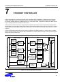
1
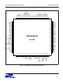
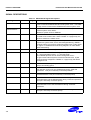
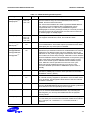
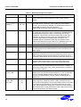
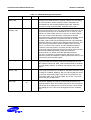
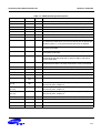
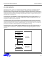
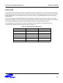
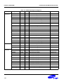
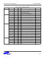
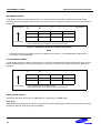
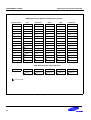
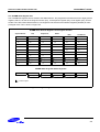
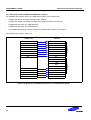
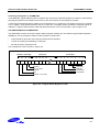
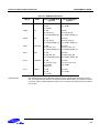
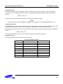
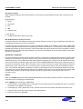
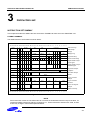
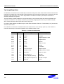
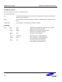
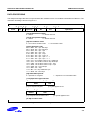
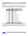
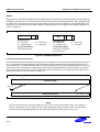
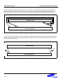
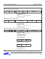
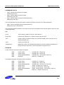
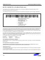
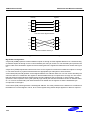
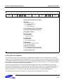
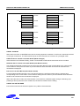
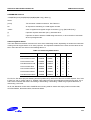
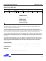
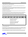
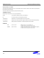
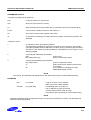
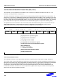
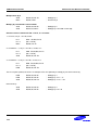
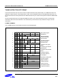
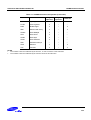
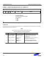
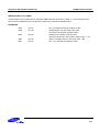
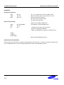
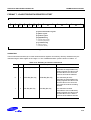
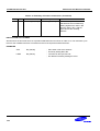
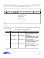
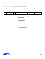
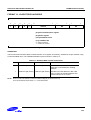
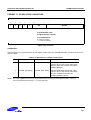
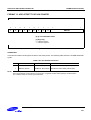
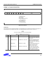
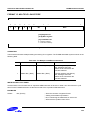
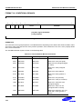
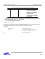
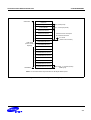
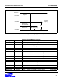
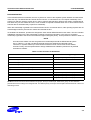
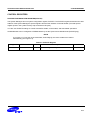
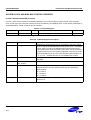
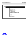
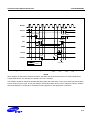
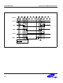
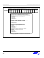
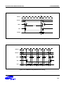
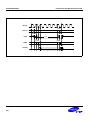
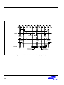
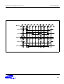
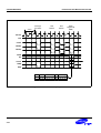
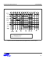
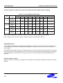
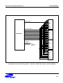
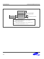
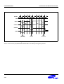
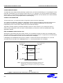
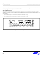
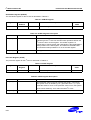
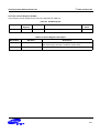
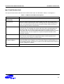
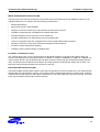
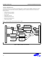
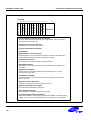
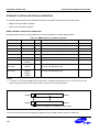
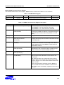
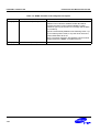
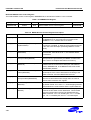
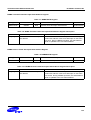
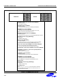
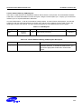
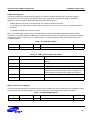
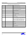
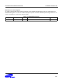
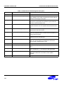
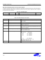
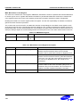
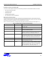
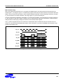
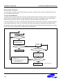
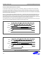
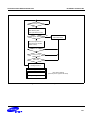
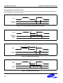
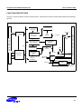
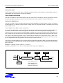
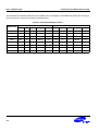
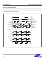
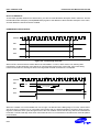
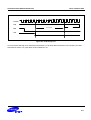
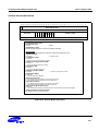
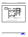
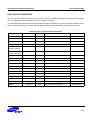
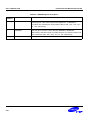
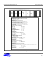
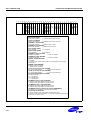
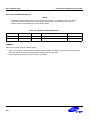
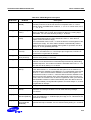
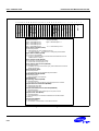
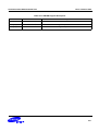
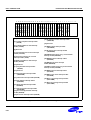
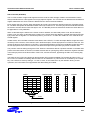
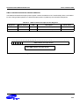
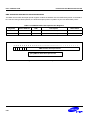
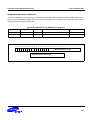
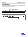
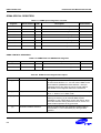
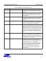
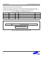
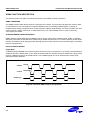
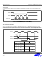
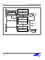
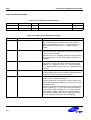
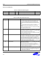
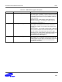
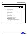
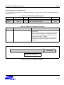
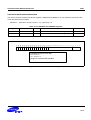
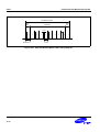
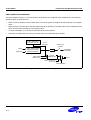
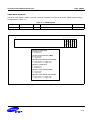
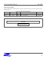
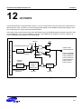
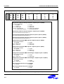
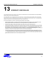
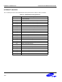
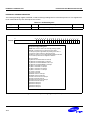
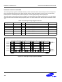
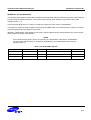
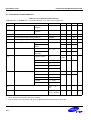
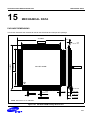
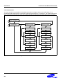
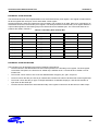
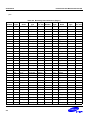
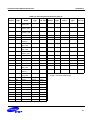
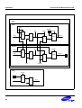
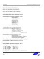
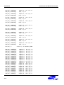
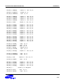
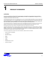
PRODUCT OVERVIEW
Pad
Type
KS32C50100 RISC MICROCONTROLLER
I/O
Type
Table 1-3 KS32C50100 PAD Type
Current
Cell Type
Drive
Feature
Slew-Rate
Control
ptic
I
–
LVCMOS Level
5V-tolerant
–
ptis
I
–
LVCMOS Schmit
Trigger Level
5V-tolerant
–
pticu
I
–
LVCMOS Level
5V-tolerant
Pull-up register
–
pticd
I
–
LVCMOS Level
5V-tolerant
Pull-down register
–
pia_bb
I
–
Analog input with
seperate bulk bias
–
–
pob1
O
1mA
Normal Buffer
–
–
ptot2
O
2mA
Tri-state Buffer
5V-tolerant
–
pob4
O
4mA
Normal Buffer
–
–
ptot4
O
4mA
Tri-state Buffer
5V-tolerant
–
ptot6
O
6mA
Tri-state Buffer
5V-tolerant
–
ptbsut1
I/O
1mA
LVCMOS Schmit trigger
level Tri-state Buffer
5V-tolerant
Pull-up register
–
ptbcut4
I/O
4mA
LVCMOS Level
Tri-state Buffer
5V-tolerant
Medium
ptbcd4
I/O
4mA
LVCMOS Level
Open drain Buffer
5V-tolerant
–
NOTE: 1. pticu and pticd provides 100K Ohm Pull-up(down) register.
For detail information about the pad type, see Chapter 4. Input/Output Cells of the "STD90/MDL90 0.35um 3.3V
Standard Cell Library Data Book", produced by Samsung Electronics Co., Ltd, ASIC Team .
nRESET
64*f MCLK
512*f MCLK
nRCS0
NOTE:
After the falling edge of nRESET, the KS32C50100 count 64 cycles for a
sysetem reset and needs further 512 cycles for a TAG RAM clear of cache.
After these cycles, the KS32C50100 asserts nRCS0 when the nRESET is
released.
Figure 1-3 Reset Timing Diagramt
1-16