1
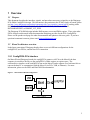
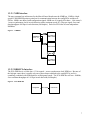
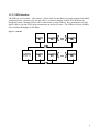
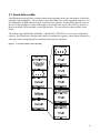
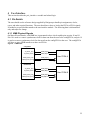
PCIe-DMA ConfigFPGA Design
User Interface Manual
8/7/2013
Rev 1.20
1
Table of Contents
1
2
3
4
5
6
7
Overview ............................................................................................................................................. 5
1.1
Purpose........................................................................................................................................ 5
1.2
Board Architecture overview ...................................................................................................... 5
1.2.1 ConfigFPGA PCIe Interface ................................................................................................... 5
1.2.2 ConfigFPGA FPGA Interface ................................................................................................. 6
Board Addressing................................................................................................................................ 9
2.1
Accessing BAR Registers ........................................................................................................... 9
2.2
Board Address Map .................................................................................................................. 11
DMA Design Details......................................................................................................................... 12
3.1
Target Reads ............................................................................................................................. 12
3.1.1 General Description .............................................................................................................. 12
3.1.2 Target Read Byte Enables ..................................................................................................... 12
3.1.3 Summary Of Typical Use Cases ........................................................................................... 12
3.1.4 Error Conditions.................................................................................................................... 13
3.2
An Overview of DMA .............................................................................................................. 13
3.3
Specifics of Dinigroup DMA Engines ...................................................................................... 13
3.4
DMA Addressing ...................................................................................................................... 14
3.5
BAR0 Registers ........................................................................................................................ 15
3.6
DMA Descriptor Format ........................................................................................................... 21
User Interface .................................................................................................................................... 22
4.1
Pin Details ................................................................................................................................. 22
4.1.1 NMB Physical Signals .......................................................................................................... 22
4.1.2 DDR PCIe Physical Signals .................................................................................................. 23
4.1.3 SFB Physical Signals ............................................................................................................ 23
4.2
Backend Signals ........................................................................................................................ 24
Demand Mode User FPGA Side Details .......................................................................................... 28
5.1
Features ..................................................................................................................................... 28
User-Level Interrupts ........................................................................................................................ 30
Other Features ................................................................................................................................... 30
2
Table of Tables
Table 1 – Change Log ................................................................................................................................. 4
Table 2 – List of Interfaces by Board ......................................................................................................... 6
Table 3 – BAR0 Address Map .................................................................................................................. 15
Table 4 – Descriptor Format ..................................................................................................................... 21
Table 5 – Backend Clocks, Resets ............................................................................................................ 24
Table 6 – User Signals .............................................................................................................................. 24
Table 7 – Demand Mode 2-Qword Descriptor Format ............................................................................. 28
Table 8 – Demand Mode dma_to_host_ctrl.............................................................................................. 29
Table 9 – Demand Mode dma_from_host_data........................................................................................ 29
Table 10 – Demand Mode dma_from_host_ctrl ....................................................................................... 29
Table of Figures
Figure 1 – Marvell-based Board Configuration .......................................................................................... 5
Figure 2 – Non-Marvell-based Board Configuration.................................................................................. 6
Figure 3 – NMB Bus ................................................................................................................................... 7
Figure 4 – PCIe DDR Bus .......................................................................................................................... 7
Figure 5 – SFB Bus ..................................................................................................................................... 8
Figure 6 – Address Translation from Host Memory to Board Address .................................................... 10
Figure 7 – User FPGA Address Space Decoding ..................................................................................... 11
Figure 8 – NMB Detail ............................................................................................................................. 22
Figure 9 – DDR PCIe Detail ..................................................................................................................... 23
Figure 10 – SFB Detail ............................................................................................................................. 23
Figure 11 – Example User Transactions ................................................................................................... 27
3
Table 1 – Change Log
Revision
1.1
1.2
1.3
1.4
1.5
Name
Brian Poladian
Brian Poladian
Brian Poladian
Brian Poladian
Brian Poladian
1.6
1.7
1.8
1.9
1.10
1.11
1.12
1.13
Brian Poladian
Brian Poladian
Brian Poladian
Brian Poladian
Brian Poladian
Brian Poladian
Brian Poladian
Brian Poladian
1.14
1.15
1.16
1.17
Brian Poladian
Brian Poladian
Brian Poladian
Brian Poladian
1.18
1.19
1.20
Brian Poladian
Brian Poladian
Brian Poladian
Details
Initial
Added board/bus interface table.
Added transaction waveform. Updated data throughput speeds.
Added DMA2 interrupts.
Added DMA addressing example. All board addresses are now byte
addresses.
Added missing BAR0 Reset register description.
Updated dma_from_host_ctrl signal description.
Fixed max memory size in descriptor address update bit description.
Added error return value descriptions.
Added legacy reset register
Updated signal definition of dma_from_host_advance
Fixed bit definition of demand-mode dma_from_host_ctrl
Better description of user interrupt register.
Accurate description of demand-mode Tag as return data address.
Added user interrupt passthrough register
Removed deprecated ‘Test bit’ from DMA0 FIFO register.
Added description of ‘User Interface Ready’ register
Added timeout value register. Elaborated description of 0xdeadbee
timeout error.
Corrected BAR0 scratch space address range.
Added BAR0 reserved debugging range.
Added interrupt enable bit to demand-mode descriptor
4
1 Overview
1.1 Purpose
This document describes the interfaces, signals, and procedures necessary to interface to the Dinigroup
PCIe-DMA ConfigFPGA design. This document is not pertinent to the PCIe8T family of boards; please
see http://www.dinigroup.com/product/common/pcie8t_user_interface_manual.pdf if working with a
DN9000K10PCIe8T, DN9002K10PCIe8T, DN9200K10PCIe8T, DN7006K10PCIe8T,
DN7406K10PCIE8T, or DNMEG_V5T_PCIE.
The Dinigroup PCIe-DMA design includes BAR memory access and DMA engines. There exist other
FPGA designs not discussed in this document that Dinigroup provides for the PCIe ConfigFPGA.
Please see the product web page for other documentation and updates to this user guide. If you have
questions/comments/concerns, please email [email protected] .
1.2 Board Architecture overview
In the latest generation of Dinigroup boards, there are several different configurations for the
configFPGA, user FPGAs, and the host PCIe connection.
1.2.1 ConfigFPGA PCIe Interface
On Marvell-based Dinigroup boards, the configFPGA connects via PCIe to the Marvell; the host
computer is not able to directly see the configFPGA’s DMA engines or register space. The
software/driver interface to the configFPGA runs on the Marvell, and a separate set of software/drivers
runs on the host PC to communicate with the Marvell (via PCIe, USB, or Ethernet). For more
information, please see the EMU and DiniCMOS documentation.
Figure 1 – Marvell-based Board Configuration
5
On non-Marvell boards (and additionally on Marvell-based boards with alternate configuration options),
the configFPGA is connected directly to the PCIe fingers, and its BAR space and DMA engines are
directly accessible from the host PC. For more information, please see the AETest documentation.
Figure 2 – Non-Marvell-based Board Configuration
configFPGA
PCIe x4
PCIe Fingers
The protocol for interfacing to the configFPGA is identical in theory and very similar in implementation
between the two configurations. Please see the Quickstart PCIe Guide for more details about the host
interface to the configFPGA.
1.2.2 ConfigFPGA FPGA Interface
The manner in which the configFPGA connects to the field (user) FPGAs varies depending on the
specific Dinigroup board. A summary of interfaces on each board is found below:
Table 2 – List of Interfaces by Board
Board
DNBFC_S12_PCIE
DNDUALV6_PCIE4
DNV6F6PCIE
DNV6_F2PCIE
DN2076K10
NMB Interfaces
0
2
6
2
7
DDR-PCIe Interfaces
1
0
0
0
0
SFB Interfaces
2
0
0
0
0
6
1.2.2.1 NMB Interface
The most common bus architecture for the Marvell-based boards uses the NMB bus. NMB is a highspeed LVDS SERDES point-to-point bus for communication between the configFPGA and the user
FPGAs. NMB is not shared with configuration signals. NMB uses 10 signals (8-bit data + 1-bit control +
1 source-synchronous clock) in each direction with a maximum speed of 1 Gbps per signal, for a total
data throughput of 8Gbps in each direction (full-duplex). Each user FPGA has its own independent
NMB bus.
Figure 3 – NMB Bus
1.2.2.2 DDR-PCIe Interface
The PCIe DDR bus is a 64-bit data + 13-bit control + source-synchronous clock DDR bus. Because of
the high pin count, there is usually only one of these busses attached to the configFPGA, and it is
commonly combined with SFB interfaces on Dinigroup boards. The PCIe DDR bus will run ~100Mhz,
for a total data throughput of 6.4 Gbps in each direction (full-duplex).
Figure 4 – PCIe DDR Bus
configFPGA
PCIe DDR
User FPGA
7
1.2.2.3 SFB Interface
The SFB bus is a 8-bit data + 4-bit control + global clock bus that shares its signals with the SelectMAP
configuration bus. Because of its low pin count, it is ideal to combine with the PCIe DDR bus on
Dinigroup boards. Multiple FPGAs can be connected to a single SFB bus, but communication is halfduplex, and so only one FPGA may communicate on the bus at a time. The SFB bus will run ~60MHz,
for a total data throughput of 480 Mbps.
Figure 5 – SFB Bus
8
2 Board Addressing
The DMA design has a consistent addressing scheme independent of the board’s physical bus
architecture; the following description is accurate for all boards.
2.1 Accessing BAR Registers
BAR0 is used for PCIe and BAR configuration, and BARs 1,2, and 4 are windows into 64-bit user
address space. The BAR windows can be moved independently and may overlap. The BAR windows
are controlled by registers on the BAR0 interface.
The 64-bit address space (address[63:0]) is comprised of three parts:
[63:32] : set by HIADDR register
[31:size_of_bar] : set by LOADDR register
[size_of_bar-1:0] : set by target address
The size_of_bar variable is set by the LOADDR_ MASK register, and by default uses the maximum
BAR size. The 64-bit board address is assembled as follows :
{HIADDR, ((LOADDR & LOADDR_MASK) | (offset & ~LOADDR_MASK))}.
Example :
Consider Figure 6 and Table 2. The physical address of BAR0 in host memory is 0xd1c00000. Suppose
we want to write to physical board address 0x01000000_02005678.
1) Map host memory address for BAR0 in host software
2) Write to BAR0 host_memory_address + 0x100 (BAR4_HIADDR register) the value of the
upper 32 bits of the address, 0x01000000
3) Write to BAR0 host_memory_address + 0x104 (BAR4_LOADDR register) the value of the
lower 32 bits of the address that fall outside the maximum size of the BAR. In this case,
BAR4 size is 16MB, and so 0x02XXXXXX needs to be written. (By default, BAR4’s
LOADDR_MASK is set to 0xFF000000).
4) The BAR4 window is now set up, and is pointing to 0x01000000_02000000. Map host
memory address for BAR4 in host software.
5) Write to BAR4 host_memory_address + 0x5678 the desired value for board address
0x01000000_02005678.
9
Figure 6 – Address Translation from Host Memory to Board Address
Host Memory
BAR0
0xd1c00000
configFPGA
Host_memory_addr + offset
User FPGA
BAR0
BAR1
0xd1800000
Host_memory_addr + offset
{BAR1_HIADDR, (BAR1_LOADDR & BAR1_LOADDR_MASK) +
offset
BAR2
0xd1000000
Host_memory_addr + offset
{BAR2_HIADDR, (BAR2_LOADDR & BAR2_LOADDR_MASK) +
offset
BAR4
0xd0000000
Host_memory_addr + offset
{BAR4_HIADDR, (BAR4_LOADDR & BAR4_LOADDR_MASK) +
offset
10
2.2 Board Address Map
Each Dinigroup board will have a unique address map depending on the type and number of interfaces
attached to the configFPGA. The top 8 bits of the 64-bit address are used to decode the interfaces. For
the NMB and PCIe DDR interfaces, there is one FPGA per interface, and that FPGA has full access to
the next 56 bits of address. On the SFB interface, the second 8 bits are used for an FPGA decode, as
there are multiple FPGAs attached to each SFB interface. The next 48 bits are then available to the
FPGA.
The address range 0xFF000000_00000000 – 0xFFFFFFFF_FFFFFFFC is reserved for configuration
registers. Each board has a document describing its configuration registers, which include registers for
setting up clocks, configuring FPGAs, and other board-specific interfaces.
Figure 7 – User FPGA Address Space Decoding
11
3 DMA Design Details
The DMA design has a consistent interface to host software independent of the board’s physical bus
architecture; the following description is accurate for all boards.
3.1 Target Reads
3.1.1 General Description
This target interface supports only dword reads and aligned quadword reads, which is all that is ever
generated by 99% of host machine chipsets. Target read TLP packets with the length field set to >2 are
not supported. Dword reads may be unaligned only if the resulting transfer does not cross a quadword
boundary. This means that a dword read may start at address 2, but not at address 6. If a dword read is
not aligned (i.e. it crosses a dword boundary), or if an aligned quadword was requested, then the signal
target_read_ctrl[0] is set. In this case, the user must return both dwords, and target_read_data_ctrl[0]
must be set when target_read_data_valid is enabled with the return data.
Return data returned in target_read_data[63:0] is expected to ALWAYS be quadword aligned,
regardless of what address is presented on target_address[63:0]. This means that if you get a dword read
(i.e. target_read_data_ctrl[0] is zero), and the address is 4, then you should return the dword from
address 4 in the UPPER 32 BITS of the return data, and the lower 32 bits is don't care. This is a little
clumsy for a 32-bit backend, but makes sense if your backend is actually 64-bit (in which case you
should ignore address bit 2).
3.1.2 Target Read Byte Enables
If your backend is not prefetchable (reads have side effects), then you can use target_read_be[7:0] in
order to access only the requested bytes in a transfer. The byte enables presented are always quadword
aligned, so if the address is 4 and the byte enables are 0x30, this means that two bytes from address 4
should be returned in target_read_data[47:32], and the rest of target_read_data is don’t care. If the
address is 8 and the byte enables are 0x3C, then 4 bytes should be returned starting at address 10. In this
case target_read_ctrl[0] will be set, because the transaction crosses the dword boundary. The typical
transaction is the aligned dword, where the address ends in 0 or 4, and the byte enables are 0x0F or 0xF0
respectively. Target_read_ctrl[0] is not set in these transactions, as the dword boundary is not crossed.
3.1.3 Summary Of Typical Use Cases
In summary, there are three typical cases for how the target read backend may be implemented:
1. 64-bit Backend. Ignore address bit 2 and always return an entire quadword. The byte enables
in target_read_be[7:0] may be ignored. Remember to always return the contents of
target_read_ctrl[7:0] onto target_read_data_ctrl[7:0] along with the data, but no special action is
needed if target_read_ctrl[0] is set.
2. 32-bit Backend. Use target_read_ctrl[0] to decide if a quadword must be returned, otherwise
return only the requested dword, in target_read_data[31:0] if the address ends in 0, or in
target_read_data[63:32] if the address ends in 4. If you can guarantee all target reads are aligned
dword transfers (i.e. you only ever dereference uint* pointers in the device driver), then you can
ignore target_read_ctrl[0] and just return the dword indicated by the address.
Target_read_ctrl[7:0] should still be returned on target_read_data_ctrl[7:0] along with the data.
The byte enables in target_read_be[7:0] may be ignored.
12
3. Reads have side effects at byte boundaries. If your design requires that you access certain
bytes within a dword without accessing other bytes in the same dword, then you may use the
byte enables in target_read_be[7:0] to mask the read. The byte enables are always quadword
aligned, so the 64-bit backend can ignore address bit 2 and return the bytes indicated by
target_read_be[7:0]. The 32-bit backend must still operate as specified in case 2 above, but in
addition should use the appropriate bits from target_read_be[7:0] to retrieve only the requested
bytes. If the address ends in 0 then target_read_be[3:0] should be used. If the address ends in 4
then target_read_be[7:4] should be used, and requested data should be returned in the upper half
of target_read_data[63:0]. If the address ends in 0 and target_read_ctrl[0] is set, then both
dwords must be accessed and the bytes specified in target_read_be[7:0] should be returned.
Target_read_ctrl[0] will never be set if the address ends in 4.
3.1.4 Error Conditions
There are two error codes generated by the PCIe core that can be returned to the host software in
place of valid data. These are retuned to in order to maintain a valid PCIe link with the host PC.
0xDEADBEE1_DEADBEE0 : read access to invalid memory space
0xDEADBEE3_DEADBEE2 : read access to valid memory space, but read timed out
If 0xffffffff_ffffffff is returned, the PCIe link itself is failing, indicating that either bad
(malformed) data is being sent from the user design to the PCIe core, or data is being returned in
response to a transaction that has already timed out. Most systems will hang soon after this
condition is hit.
If 0xdeadbee3_deadbee2 is being returned but the user design is correctly returning data, the
timeout cycle count may be too low. Generally, target reads should return immediately because
the host PC CPU will stall while the read is pending, and it’s not a good idea to stall the CPU for
extended periods of time. Therefore it is assumed that most designs that do not return data
immediately after a read request have some other (protocol) problem; if this is not the case and the
user logic simply takes a long but finite time to return data, the timeout value BAR0 register can
be given a larger value.
3.2 An Overview of DMA
DMA engines move data. DMA is a method of moving data without using a CPU to do the reads and
writes. It also allows for bursting of data, which is usually not possible with CPU reads and writes.
A DMA engines uses descriptors to tell it what to do. A descriptor contains a length, source address,
and destination address. It generally also contains flags/status to do different variants of data transfer,
and to report back success or failure. The DMA engine uses this information to execute read or write
requests, to move data from one place to another. The DMA engine also needs to know how to get
descriptors and how to tell if they contain valid data or not.
3.3 Specifics of Dinigroup DMA Engines
There are three (3) independent DMA engines in the Dinigroup DMA design. Each is controlled using
BAR0 registers; the physical address of host memory will be written into the DMA control registers and
the DMA engines will then fetch descriptors from those addresses.
13
A valid bit is used in the descriptor to tell if the descriptor is valid or not. Software sets the valid bit to 1
when the 4-dword descriptor contains valid data. Hardware sets the valid bit to 0 when hardware is
done moving the data. The descriptors in host memory are stored in a contiguous circular queue.
Software simply tells the DMA engine the base address and size mask of the circular queue, and then
hardware has enough information to fetch descriptors and process them. It is the responsibility of
software to make sure that the tail of the queue is never overwritten.
Note that all addresses given to the DMA engine (both the descriptor queue base address and the PCIe
addresses in the descriptors) must be physical addresses. The DMA engine has no means to translate
logical addresses to physical addresses.
Queue terminology: Head is where the software writes the next valid descriptor. Tail is where hardware
clears the descriptor when the transfer is complete. Top is the base address of the queue. Bottom is the
last valid address in the queue, where software must “loop”, so Bottom + 1 == Top.
3.4 DMA Addressing
All data will be aligned to a 64-bit data path. DMA transfers that begin on a non-64-bit-aligned address
will be pre-padded to be 64-bit-aligned address compatible, but the non-aligned address will be passed
to the user design – the user is then free to use or ignore the non-aligned part of the address.
Example #1: 64-bit-aligned access:
Address: 0x0
Length (32-bit dwords): 5
Data[63:0] :
data[0x4], data[0x0]
data[0xc], data[0x8]
xxxxxxxx, data[0x10]
Example #2: non-64-bit-aligned access:
Address: 0x4
Length (32-bit dwords): 5
Data[63:0] :
data[0x4], xxxxxxxxx
data[0xc], data[0x8]
data[0x14], data[0x10]
DMA from_host data will be aligned by the PCIe core. DMA to_host data should be similarly aligned
by the user.
14
3.5 BAR0 Registers
BAR Address map:
BAR0: 32-bit BAR; PCI-E FPGA registers, blockRAM (1MB)
BAR1: 32-bit BAR; User FPGA (4 MB)
BAR2: 64 bit BAR; User FPGA (8MB)
BAR4: 64 bit BAR; User FPGA (16MB)
Table 3 – BAR0 Address Map
Byte Addr
Name
Bit Definitions
Detailed Description
0x000 R
Version
Number
[31:16] Major Rev.
Version Number of PCI-E FPGA design
currently loaded.
[15:0] Minor Rev.
Current value is 0x0001_0043.
0x004 R
Date
YYYY_MMDD
Date that this design was created/built.
Example value is 0x2007_0718
0x008 R
0x00C RW
Design Type
Reset Control
ASCII of Bitstream
Type.
Possible values are “Full” = 0x4675_6C6C or
[0] BAR0 Reset
BAR0 Reset is a user-controllable active reset
that will cause User Reset to be asserted. User
Reset is a read-only signal that is asserted either
by BAR0 Reset or when internal clocks are not
ready; User Reset will reset all user interface
modules. TRN Reset is a read-only signal that is
asserted by the Xilinx PCIe core while the PCIe
core is not ready for transactions.
[1] User Reset
[2] TRN Reset
0x010 RW
Reset Control
[0] BAR0 Reset
(Legacy)
[1] User Reset
“DMEG” = 0x444D_4547.
Same control as 0xC. Register added for V6/V5
register map compatibility.
[2] TRN Reset
0x018 RW
LED Control
[7:0] LED out [7:0]
[15:8] LED en [7:0]
Bits [15:0] and [25:24] are R/W; Bits [23:16]
and [26] are read only.
[23:16] LED in [7:0]
[24] LED out [8]
LED order :
[25] LED en [8]
{pcie_debug_led[3:0], yellow_activity, red_los,
green_link8, green_link4, green_link1}
[26] LED in [8]
15
0x020 R/W
DMA0 Base
Address0
[31:12] Base
Address
[11:0] 0x000
Lower 32 bit byte address of physical address (in
host memory) where the DMA0 descriptor chain
starts. This address must have the lower bytes
cleared to match the DMA0 Address Mask
register.
0x024 RW
DMA0 Base
Address1
[31:0] Base Address
Upper 32 bits of Base Address[63:0], to form a
64 bit address. Set to 0 if using 32 bit
addressing.
0x028 RW
DMA0
Address Mask
[19:12] Address
Mask
Address mask to indicate size of Descriptor list.
Set some number of consecutive lower bits to 1.
Set to the size of the list in bytes, minus 1. For
example, for an 8KB descriptor list, set this to
8K-1=0x01FFF.
[11:0] 0xFFF
0x02C RW
DMA0
Control
[9:0] re-read time in
milliseconds
10: DMA enable
11: DMA clear
12: DMA Demand
Mode enable
Re-read time is the time between checks for a
valid bit in the next descriptor in the list. This
value cannot be set to 0. If software tries to set
this to zero, it will be set to one. Default value is
1.
DMA enable enables the DMA engine.
DMA clear clears the DMA engine, resetting the
address counters to the base address and clearing
any running transactions. Software must set this
back to zero to bring the DMA engine out of
“reset”.
DMA Demand Mode enables the User FPGA to
initiate to-host and from-host DMA transfers
0x030 W
DMA0 Poll
Immediate
0: Poll Immediate
Writing a 1 to this register causes the DMA
engine to fetch the next descriptor from the host
immediately (and not wait for the re-read timer
to expire).
0x034 R
DMA0 Read
Address
[31:0] Current Read
Address
DEBUG INFO ONLY: The lower 32 bits of the
current address being read, or the next address
that will be read.
0x038 R
DMA0
Execute
Address
[31:0] Current
Execute Address
DEBUG INFO ONLY: The lower 32 bits of the
address of the descriptor currently being worked
on. Because of multiple reads pending, we could
have subsequent descriptors also being worked
on at the same time.
16
0x03C R
DMA0
Descriptor
FIFO Info
[9:0] Descriptor
FIFO empty count
DEBUG INFO ONLY: Number of elements
(qwords) in the descriptor FIFO. Note there
could be more descriptors still pending in the
system that have already been read out of this
FIFO.
0x0400x05C
Repeat for
DMA1
0x0600x07C
Repeat for
DMA2
0x080 R
TRN Clock
Counter
[31:0] Clock
Counter
Counter for clock from Xilinx Block Plus Core
on TRN interface.
0x084 R
Internal Clock
Counter
[31:0] Clock
Counter
Counter for clock to internal DMA engines, TLP
state machine, etc.
0x088 R
User Clock
Counter
[31:0] Clock
Counter
Counter for clocks to the user interfaces.
0xA0 R
User Interface
Ready
[0] FPGA A ready
Shows if the user interface to the field FPGAs is
ready for data transfer. Each bit corresponds to a
single FPGA – FPGAs not stuffed or present on
a board will have a value of 0 for that bit. For
NMB links, this bit signifies that the NMB link
has trained successfully. For SFB links, this bit
signifies that the SFB link has trained
successfully and that the device is responding to
polling. For PCIe-DDR links, this bit signifies
that reset is not asserted.
[1] FPGA B ready
…
[31] Configuration
registers ready
0xC0
TRN Debug
Status
Subject to Change
DEBUG INFO ONLY: Contact Dinigroup for
access to debug information.
0xC4
DMA Debug
Status
Subject to Change
DEBUG INFO ONLY: Contact Dinigroup for
access to debug information.
0xC8
User BAR
Debug Status
Subject to Change
DEBUG INFO ONLY: Contact Dinigroup for
access to debug information.
0xCC
User DMA
Debug Status
Subject to Change
DEBUG INFO ONLY: Contact Dinigroup for
access to debug information.
17
0x0D0 R/W Interrupt
[0] DMA0 To Host
Interrupt
[1] DMA0 From
Host Interrupt
[2] DMA1 To Host
Interrupt
[3] DMA1 From
Host Interrupt
In Legacy Interrupt mode, a value of 1 means
that this interrupt event occurred. Software
needs to write a 1 to the corresponding bit to
clear the interrupt.
In MSI interrupt mode, these bits are selfclearing once the MSI interrupt message is sent.
The vector number send per interrupt depends on
the number of vectors allocated to the card, and
will be defined in a future version of the design.
[4] DMA0 Going
Idle
[5] DMA1 Going
Idle
[6] DMA2 Going
Idle
[7] DMA2 To Host
Interrupt
[8] DMA2 From
Host Interrupt
0xD4 RW
Interrupt Mask
[8:0] Mask Control
for Interrupt Bits
A value of 1 in the mask means that the
corresponding interrupt source generates an
interrupt over the PCI-E bus. A value of 0
means the corresponding interrupt bit doesn’t
create an interrupt event.
0xE0 RW
User Interrupt
Passthrough
[31:0] Passthrough
Control
A value of 1 means that the latch on User
Interrupts is disabled, and the interrupt condition
will clear as soon as the User Interrupt in the
user FPGA is cleared. The default value of 0
enables the latch and is recommended to prevent
spurious interrupts.
0xE8 RW
User Interrupt
[31:0] User
Interrupts
In Legacy Interrupt mode, a value of 1 means
that this interrupt event occurred. Software
needs to write a 1 to the corresponding bit to
clear the interrupt.
In MSI interrupt mode, these bits are selfclearing once the MSI interrupt message is sent.
The vector number send per interrupt depends on
the number of vectors allocated to the card, and
will be defined in a future version of the design.
18
0xEC RW
User Interrupt
Mask
[31:0] Mask Control
for User Interrupt
Bits
A value of 1 in the mask means that the
corresponding interrupt source generates an
interrupt over the PCI-E bus. A value of 0
means the corresponding interrupt bit doesn’t
create an interrupt event.
0xF0 RW
BAR1 Upper
Address
[31:0] Address
Upper 32 bits of 64-bit target address for BAR1.
0xF4 RW
BAR1 Lower
Address
[31:0] Address
Lower 32 bits of 64-bit target address for BAR1.
Use mask register to control how many bits this
register actually controls.
0xF8 RW
BAR2 Upper
Address
[31:0] Address
Upper 32 bits of 64-bit target address for BAR2.
0xFC RW
BAR2 Lower
Address
[31:0] Address
Lower 32 bits of 64-bit target address for BAR2.
Use mask register to control how many bits this
register actually controls.
0x100 RW
BAR4 Upper
Address
[31:0] Address
Upper 32 bits of 64-bit target address for BAR4.
0x104 RW
BAR4 Lower
Address
[31:0] Address
Lower 32 bits of 64-bit target address for BAR4.
Use mask register to control how many bits this
register actually controls.
0x108 RW
BAR1 Lower
Address Mask
[31:0] Mask
Sets number of bits that lower 32-bit address
register controls. Defaults to 0xFFC0_0000.
0x10C RW
BAR2 Lower
Address Mask
[31:0] Mask
Sets number of bits that lower 32-bit address
register controls. Defaults to 0xFF80_0000.
0x110 RW
BAR4 Lower
Address Mask
[31:0] Mask
Sets number of bits that lower 32-bit address
register controls. Defaults to 0xFF00_0000.
0x120 RW
BAR Timeout
Value
[31:0] Timeout
Value
Number of cycles to wait for a read response to
be generated by user code before returning an
0xDEADBEE2_DEADBEE3 timeout value.
Defaults to 0x00000FFF (4K clock cycles).
0x140 R
Interface 0
Timeout
[31:0] Timeout
Counter
Number of read timeouts handled on Interface 0.
Mapping of interface to FPGA varies by board.
0x144 R
Interface 1
Timeout
[31:0] Timeout
Counter
“
0x148 R
Interface 2
Timeout
[31:0] Timeout
Counter
“
0x14C R
Interface 3
Timeout
[31:0] Timeout
Counter
“
19
0x150 R
Interface 4
Timeout
[31:0] Timeout
Counter
“
0x154 R
Interface 5
Timeout
[31:0] Timeout
Counter
“
0x158 R
Interface 6
Timeout
[31:0] Timeout
Counter
“
0x15C R
Interface 7
Timeout
[31:0] Timeout
Counter
“
0x2000x2FC R
Reserved
Reserved
Reserved for internal debugging purposes.
[31:0] Block RAM
data
Read/Write “scratch pad” space.
0x300Block RAM
0x7FC R/W
20
3.6 DMA Descriptor Format
Table 4 – Descriptor Format
Dword
Bit
Number
Number
Name
0
31
Valid
0
30
Direction
0
29
Generate Interrupt
0
28
Set Registers Type
0
0
27:26
25
0
24
0
23:0
Byte Length[25:2]
1
31:0
Board Address[31:0]
2
31:0
PCI Address[31:2], 00
3
31:0
PCI Address[63:32]
RSVD
Overflow
Transfer Complete
Description
Bit indicating if the descriptor is valid. Software sets
this to 1 when the descriptor is ready to be processed
(Other dwords of the descriptor written, memory
pointed to by PCI Address available), Hardware clears
this to 0 when the descriptor has been processed
completely. Software may not modify ANYTHING
in the descriptor once the valid bit has been set to
1.
0 = From_Host (Move data from PCI Address to
Board Address)
1 = To_Host (Move data from Board Address to PCI
Address)
If 1, hardware will interrupt software once this
descriptor has been processed completely. Bit is
ignored when Set Registers Type is 1.
Set to 1 to set High Bits of Board Address. Does not
transfer any data. Used to access more than 4 GB of
memory space on the user side. This sets distinct
registers depending on the value of the Direction Bit
(To_host and From_host can have different high bits
of the board address).
Reserved/unused/undefined. Set to 0 for future
backward compatibility.
When set, User returned more data than expected.
Status bit (set by Hardware). To_Host direction only,
indicates user FPGA indicated this is end of the data
for this transfer.
Valid values are 4 bytes (value of 1) to 64M-4 bytes.
This length must indicate a contiguous block of
memory in PCI address space and user address
space.
Byte Address to read or write from on the board (user
side address space). When bit [28] is asserted, this is
the upper 32 bits of a 64-bit board byte address.
Physical address to read or write data in host
memory. Note that the data must be address
contiguous for this entire transfer.
Upper 32 bits of PCI physical Address. If software is
using 32 bit addressing, this must be set to 0.
21
4 User Interface
This section describes the pcie_interface.v module and related logic.
4.1 Pin Details
The user should use the reference design supplied by Dinigroup to handle pin assignments, clocks,
resets, and other required functions. The user should never have to look at the FPGA to FPGA signals;
IO modules are provided that attach to the user interface module. The following data is informational
only and subject to change.
4.1.1 NMB Physical Signals
On Marvell-based boards, each NMB bus is guaranteed to have clock-capable pins on pairs 18 and 19.
Pair 18 is used as a source-synchronous clock for data sent from the user to the configFPGA, and pair 19
is used as a source-synchronous clock for data sent from the configFPGA to the user. The configFPGA
will have as many NMB interfaces as there are FPGAs.
Figure 8 – NMB Detail
configFPGA
INTERFACE 0
TO_HOST_CLK
NMB_QA[18]
TO_HOST_DATA
NMB_QA[8:0]
FROM_HOST_CLK
NMB_QA[19]
FROM_HOST_DATA
NMB_QA[17:9]
User FPGA A
INTERFACE1
TO_HOST_CLK
NMB_QB[18]
TO_HOST_DATA
NMB_QB[8:0]
FROM_HOST_CLK
NMB_QB[19]
FROM_HOST_DATA
NMB_QB[17:9]
User FPGA B
22
4.1.2 DDR PCIe Physical Signals
The DDR PCIe bus uses a 38-bit bus in the TO_HOST direction with a source-synchronous clock, and a
39-bit bus in the FROM_HOST direction with a source-synchronous clock. Data sent on the bus is
DDR.
Figure 9 – DDR PCIe Detail
configFPGA
INTERFACE 0
TO_HOST_CLK
TO_HOST_CLK
TO_HOST_DATA
TO_HOST_DATA[38:0]
User FPGA A
FROM_HOST_CLK
FROM_HOST_CLK
FROM_HOST_DATA
FROM_HOST_DATA[37:0]
4.1.3 SFB Physical Signals
The SFB interface uses the data, chip select, busy, init, and read/write configuration signals used for
SelectMAP FPGA programming. Individual chip selects are used for every FPGA on the bus, and the
remaining signals are shared.
Figure 10 – SFB Detail
configFPGA
User FPGA F0
User FPGA F1
SFB_CS0
SFB_CS1
SFB_DATA[7:0]
SFB_BUSY
SFB_INIT
SFB_RDWR
23
4.2 Backend Signals
Here we discuss the signals in and out of the xxx_user_interface. The user must instantiate this module
in order to interface with the configFPGA. This module will have contained within it connections to
either a PCIe DDR, NMB, or SFB IO module, which will convert the physical interface to the internal
interface described here. Direction of ports described is in relation to the user_interface module.
Table 5 – Backend Clocks, Resets
Signal
Name
Direction Description
reset
Input
Main module reset. Input from user. Allows resetting the module from an
external source.
reset_out
Output
Reset to user module. When de-asserted this indicates that the interface is
ready to use.
user_clk
Input
User clock. Clocks logic on the user side of the interface. Can be sourced by
clk_out.
clk_out
Output
Clock sent to user. Clocks logic on the physical side of the interface.
Table 6 – User Signals
Signal Name
Direction Description
Target Interface
target_address[63:0]
Output
Byte address (bits 1:0 always 0)
target_address_valid
Output
One clock cycle strobe that indicates the target_address is
valid
target_write_data[63:0]
Output
Data.
target_write_be[7:0]
Output
Byte enables, bit 0 means data[7:0] is valid, etc.
target_write_enable
Output
Indicates valid write data on this interface.
target_write_accept
Input
Accepts the valid write data. Data is allowed to transfer
when target_write_accept and target_write_enable are active.
If connecting to blockRAM, this signal can be tied high.
debug_target_bar[2:0]
Output
Valid for reads and writes. Indicates which bar is being
accessed (bar number 1, 2, or 4). Onehot, so 3’b001 means
BAR1, 3’b010 means BAR2, and 3’b100 means BAR4. To
treat target_address as a unified 64-bit address space, this
signals should be used for debug/informational purposes
only.
target_read_enable
Output
High on a target read request.
24
target_request_tag[3:0]
Output
Tag associated with this read request.
target_read_accept
Input
Acceptance of read request. Allows interface to “move on”
before the read data is returned by the user.
Target_read_enable and target_read_accept being high
signals “transfer” of request. If connecting to blockram, this
signal can be tied high.
target_read_data[63:0]
Input
Read Data to return to configFPGA.
target_read_be[7:0]
Output
Byte enables, bit 0 means data[7:0] is requested, etc.
target_read_data_tag[3:0]
Input
Tag that accompanies this data. This value must match the
value provided on target_request_tag when
target_read_enable was high.
target_read_data_valid
Input
Clock cycle pulse indicating read data is valid.
target_read_ctrl[7:0]
Output
Tag associated with a target read. Bit [0] indicates both
dwords are requested (non-dword aligned or quadword
transfer)
target_read_data_ctrl[7:0]
Input
Tag associated with a target read. User must save
target_read_ctrl[7:0] when target_read_enable is asserted and
return it on target_read_data_ctrl[7:0]
DMA0 Interface
dma0_from_host_data[63:0] Output
Address, length, or data, depending on the state of
dma0_from_host_ctrl[5,0].
dma0_from_host_ctrl[7:0]
Bit meanings:
Output
[5], [0] indicates type of data.
[3:2] are dword enables (when bit 3 is 1, 63:32 is valid, when
bit 2 is 1, 31:0 is valid)
[4] indicates read request when 1, write request when 0.
Signal valid during length phase of transfer ([5],[0]==’b10)
[1], [6], [7] reserved.
Decode of [5],[0]:
01: 64 bit board byte address.
10: 24 bits of dword length [23:0]. Upper 40 bits are
reserved. For reads, user must return this many dwords of
data, properly aligned based on bit 0 of the dword board
address. For writes this information is provided but
informational only. Read/write request bit is valid here.
00: Data
11: Reserved/Undefined/Never Occurs.
25
dma0_from_host_valid
Output
Indicates valid data on data and ctrl signals.
dma0_from_host_advance
Input
Indicates that the user design is ready to accept more data –
the PCIe core will stop sending data when this signal is
deasserted. This signal is intended to attach to an almost-full
signal; dma0_from_host_valid may be asserted for several
clock cycles after dma0_from_host_advance is deasserted
due to pipelining delays.
dma0_to_host_data[63:0]
Input
Data to return to PCI-E FPGA.
dma0_to_host_ctrl[7:0]
Input
Bit meanings:
1:0 are dword enables (when bit 1 is 1, 63:32 is valid data,
when bit 0 is 1, 31:0 is valid data).
3: Indicates last data for this read request.
Bits 2, 4-7 are reserved.
dma0_to_host_valid
Input
Indicates valid data on data and ctrl signals.
dma0_to_host_almost_full
Output
When high, user should stop writing data to the module soon.
Same
Same as DMA0, but ‘1’ in the name instead of ‘0’. Separate
interfaces for each DMA engine.
Same
Same as DMA0, but ‘2’ in the name instead of ‘0’. Separate
interfaces for each DMA engine.
Input
A parameterizable number of user-level interrupts, which
will be combined into a single interrupt and sent to the PCIe
core. Interrupts can either be pulses or levels.
DMA1 Interface
Same as DMA0
DMA2 Interface
Same as DMA0
User Interrupts
user_interrupts [?:0]
26
Figure 11 – Example User Transactions
27
5 Demand Mode User FPGA Side Details
5.1 Features
All three DMA engines support Demand Mode (“Posted”) transfers initiated by user FPGA. In this
mode, descriptors come from user FPGA and are not stored in host memory as in the “normal” mode.
The DMA engine can only support one of the 2 modes; the user sets the mode by writing to a BAR0
register that defaults to “normal” mode. It is assumed that once demand mode is turned on it will stay
on (until user reset).
To-host transactions support byte enables for the first and last dword.
User FPGA starts a demand mode to-host transfer by writing a 2-qword descriptor (with PCI address,
size) to the dma_to_host* interface followed by data, when the write is complete on the PCIe side a 2qword write complete descriptor would return on the dma_from_host* interface. For a demand mode
from-host transfer, User FPGA writes a 2-qword descriptor to the dma_to_host* interface, then
dma_from_host* would return a 2-qword descriptor followed by read data.
Table 7 – Demand Mode 2-Qword Descriptor Format
Qword
Bits
Number
Location
Name
0
0
63:32
31
0
30
Direction
0
0
0
29
28
27
Generate Interrupt
Reserved
Reserved
0
0
26
25:24
0
23:0
Dword size / byte enables
63:0
PCI Address[63:0]
1
Tag
Valid
Dword Byte enables
Reserved
Description
A tag to be associated with this transfer, the same tag
would be returned with the write complete or read
complete descriptor for this transaction. The Tag can
be used as a 32-bit aligned return data board
address, and all return data will be aligned
accordingly. In order to bypass this function and use
the Tag as an indicator only, keep Tag[2:0]=3’b000.
Must be 1
0 = From_Host (Move data from PCI Address to User
FPGA)
1 = To_Host (Move data from FPGA to PCI Address)
If 1, hardware will interrupt software once this
descriptor has been processed completely.
Must be 0
Must set to 0
Set to make this transaction a to-host transfer with
byte enables, the enables are in bits [23:16]
Must be 0
Number of dwords to transfer This length must
indicate a contiguous block of memory in PCI address
space and user address space.
If this is a byte enables transaction (Bit 26 is set) bits
[23:20] are the byte enables for the first (or only)
dword, bits [19:16] are byte enables for the last
dword, they must not be 0. The number of dwords to
transfer is in bits [15:0].
If this is not a byte enables transaction (Bit 26 is not
set), [23:0] is the number of dwords to transfer.
PCI address for the transfer. If software is using 32
bit addressing, bits [63:32] must be 0.
28
Table 8 – Demand Mode dma_to_host_ctrl
Bits
Signal Name
Location
Name
dma_to_host_ctrl
0
Lower dword valid
1
2
Upper dword valid
Demand Mode Enable
3
Last
4
Descriptor Enable
Description
dma_to_host_data[31:0] is valid, if the transfer
ends with a odd dword, this should be high.
dma_to_host_data[63:32] is valid, if the transfer
ends with a odd dword, this should be low.
Always set to 1 in demand mode
Set with the last data on a to-host transfer, set on
nd
the 2 qword for the descriptor on a from-host
transfer
Set during writing of the 2-qword descriptor for
both to-host and from-host transfers. Set to 0
when transferring write (to-host) data
After a to-host or from-host transfer, a 2-qword descriptor would be returned on dma_from_host* (when
dma_from_host_valid is asserted), for from-host transfers, read data would follow.
Table 9 – Demand Mode dma_from_host_data
Qword
Bits
Number
Location
Name
0
1
31:0
23:0
Tag
Dword Size
Table 10 – Demand Mode dma_from_host_ctrl
Bits
Signal Name
Location
Name
dma_from_host_ctrl
0
Start of descriptor
2
Lower dword valid
3
Upper dword valid
4
Is Write Complete
5
End of descriptor
Description
The tag associated with this transfer, the same tag on
the 2-qword descriptor when the User FPGA initiated
the transfer.
Dword size of the transfer.
Description
Set when this is the first qword of the 2-qword
descriptor.
dma_from_host_data[31:0] is valid, , can be low
only in the first qword or last qword of the read
(from-host returned) data.
dma_from_host_data[63:32] is valid, can be low
only in the first qword or last qword of the read
(from-host returned) data.
Set if this is a to-host complete descriptor,
otherwise it’s a from-host complete descriptor,
read data would follow a from-host complete
descriptor.
Set when this is the second qword of the 2qword descriptor.
29
6 User-Level Interrupts
The user_interrupts port should be used to signal that an even has happened in user-space and trigger
the interrupt handler in the driver. The number of inputs to the interface is defined as a parameter in
user interface module. Interrupt inputs can either be pulses (at least one clock cycle in length) or can be
held in an active state. The port is active high.
One interrupt will be issued to the PCIe core for every set of interrupts that is received from the user in
the time between interrupt-handler calls. For this reason, all active interrupts must be handled on each
interrupt-handler call; a new interrupt will not be issued for any interrupt that was previously not
handled. For further details, please reference the driver code.
There are a maximum of 32 user-interrupt signals viewable in the BAR0 register. Signals from the user
modules are combined so that each FPGA’s interrupts show up as a single signal in the BAR0 register.
For example, any user_interrupt signal asserted in the user interface module in FPGA A will result in bit
[0] being asserted; FPGA B will assert bit [1], and so on.
If the passthrough register is set, the user interrupt will not be latched and the interrupt condition will
clear as soon as the user FPGA condition is cleared. This allows the mask and interrupt control logic to
reside completely in user space, but spurious interrupts may occur after the interrupt condition is cleared
but the assertion has yet to flush from the interrupt pipeline.
7 Other Features
If you have a new feature request or feel that an essential function is missing, please contact
[email protected] .
30