1
TC1793
Electrical ParametersDC Parameters
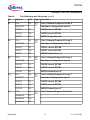
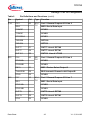
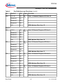
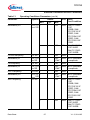
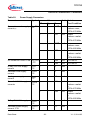
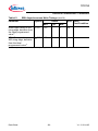
Table 18
Standard_Pads Class_A2 (cont’d)
Parameter
Symbol
Output voltage low class
A2 pads
VOLA2
Values
Min.
Typ.
Max.
−
−
0.4
Unit
Note /
Test Condition
V
IOL≤ 2 mA; pin
CC
out
driver= medium
−
−
0.4
V
IOL≤ 2 mA; pin
out
driver= strong
−
−
0.4
V
IOL≤ 500 μA;
pin out
driver= weak
1) Hysteresis is implemented to avoid metastable states and switching due to internal ground bounce. It can´t be
guaranteed that it suppresses switching due to external system noise.
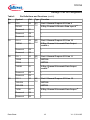
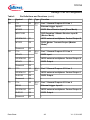
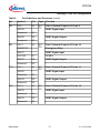
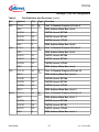
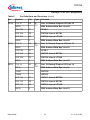
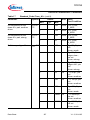
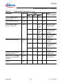
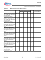
Table 19
Standard_Pads Class_B
Parameter
Input Hysteresis, B class
pads1)
Symbol
Values
Unit
Note /
Test Condition
−
V
VDDEBU= 2.5 V
−
−
V
VDDEBU= 3.3 V
Min.
Typ.
Max.
HYSB
0.08 x
−
CC
VDDEBU
0.1 x
VDDEBU
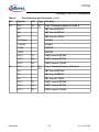
Input Leakage Current,
class B pads
IOZB CC -6000
−
6000
nA
else
-3000
−
3000
nA
(VDDEBU/2 0.6 V) < Vi < (V
Ratio between low and
high input threshold
VILB /
0.6
VIHB CC
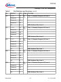
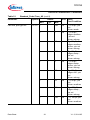
RDSONW −
−
−
450
600
Ohm IOH> -0.5 mA;
P_MOS
−
210
340
Ohm IOL< 0.5 mA;
N_MOS
−
−
155
Ohm IOH> -2 mA;
P_MOS
−
−
110
Ohm IOL< 2 mA;
N_MOS
DDEBU/2
On-Resistance of the
class B pad, weak driver
On-Resistance of the
class B pad, medium
driver
Data Sheet
CC
RDSONM
CC
115
+ 0.6 V)
V 1.2, 2014-05