1
TC1793
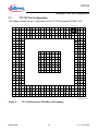
PinningTC1793 Pin Configuration
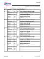
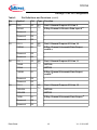
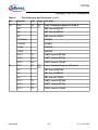
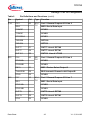
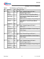
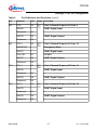
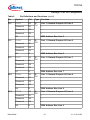
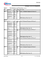
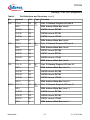
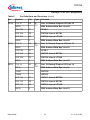
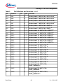
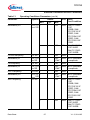
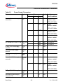
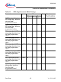
Pin Definitions and Functions (cont’d)
Table 2
Pin
Symbol
Ctrl.
Type Function
B7
P0.4
I/O
HWCFG4
I
A1/
PU
OUT60
O1
OUT60 Line of GPTA0
OUT60
O2
OUT60 Line of GPTA1
EVTO0
O3
MCDS Output Event 01)
P0.5
I/O
HWCFG5
I
OUT61
O1
OUT61 Line of GPTA0
OUT61
O2
OUT61 Line of GPTA1
EVTO1
O3
MCDS Output Event 11)
P0.6
I/O
HWCFG6
I
OUT62
O1
OUT62 Line of GPTA0
OUT62
O2
OUT62 Line of GPTA1
EVTO2
O3
MCDS Output Event 21)
P0.7
I/O
HWCFG7
I
OUT63
O1
OUT63 Line of GPTA0
OUT63
O2
OUT63 Line of GPTA1
EVTO3
O3
MCDS Output Event 31)
P0.8
I/O
Reserved
O1
Reserved
O2
-
Reserved
O3
-
A6
B6
C8
C7
Data Sheet
A1/
PU
A2/
PU
A1/
PU
A1/
PU
Port 0 General Purpose I/O Line 4
Hardware Configuration Input 4
Port 0 General Purpose I/O Line 5
Hardware Configuration Input 5
Port 0 General Purpose I/O Line 6
Hardware Configuration Input 6
Port 0 General Purpose I/O Line 7
Hardware Configuration Input 7
Port 0 General Purpose I/O Line 8
-
17
V 1.2, 2014-05