1
TPUMASMREF/D
REV 3
Time Processor Unit
Macro Assembler
(TPUMASM)
Reference Manual
PRELIMINARY
This document contains information on a product under development. Motorola reserves the right to change or
discontinue this product without notice.
Motorola reserves the right to make changes without further notice to any products herein to improve reliability,
function, or design. Motorola does not assume any liability arising out of the application or use of any product or
circuit described herein; neither does it convey any license under its patent rights nor the rights of others. Motorola
products are not designed, intended, or authorized for use as components in systems intended for surgical implant into
the body, or other applications intended to support or sustain life, or for any application in which the failure of the
Motorola product could create a situation where personal injury or death may occur. Should Buyer purchase or use
Motorola products for any such unintended or unauthorized application, Buyer shall indemnify and hold Motorola and
its officers, employees, subsidiaries, affiliates, and distributors harmless against all claims, costs, damages, and
expenses, and reasonable attorney fees arising out of, directly or indirectly, any claim of personal injury or death
associated with such unintended or unauthorized use, even if such claim alleges that Motorola was negligent regarding
the design and manufacture of the part.
Motorola and the Motorola Logo* are registered trademarks of Motorola Inc. Motorola Inc. is an Equal
Opportunity/Affirmative Action Employer.
1993, 1994, 1996, MOTOROLA, INC.; ALL RIGHTS RESERVED
CONTENTS
CONTENTS
CHAPTER 1 TPU DESCRIPTION
1.1 The Microcode Control Store
1.1.1 Microcode Segments
1.1.2 The Entry Point Segment
1.2 The Microengine
1.3 The Execution Unit
1.4 The Channels
1.5 The Parameter RAM
7
8
10
10
12
12
14
14
CHAPTER 2 ASSEMBLY LANGUAGE
2.1 Executing the Assembler
2.1.1 Option /NOLIST
2.1.2 Option /NOSREC
2.1.3 Option /SRECWIDTH
2.1.4 Option /SRECTYPE
2.1.5 Option /SRECBASE
2.1.6 Option /PAGELENGTH
2.1.7 Option /NOTABLES
2.1.8 Option /HALT
2.1.9 Option /MAXERRORS
2.2 Syntax
2.2.1 Notation
2.2.2 Comments
2.2.3 Immediate Data
2.2.4 Numeric Addresses
2.2.4 Identifiers
2.2.5 Microinstructions
2.2.6 Macros
2.3 Assembler Directives
%ENTRY Directive
%INCLUDE Directive
%MACRO Directive
%ORG Directive
%PAGE Directive
%TYPE Directive
2.4 Assembler Subinstructions
au Subinstruction
call Subinstruction
chan Subinstruction
dec_return Subinstruction
end Subinstruction
goto Subinstruction
if Subinstruction
nop Subinstruction
17
17
17
17
17
18
18
18
18
18
18
19
19
19
20
20
20
21
21
21
22
24
25
26
27
28
29
30
37
39
43
44
45
46
48
3
TPUMASMREF/D REV 3
CONTENTS
CHAPTER 2 ASSEMBLY LANGUAGE (Continued)
ram Subinstruction
repeat Subinstruction
return Subinstruction
49
51
52
CHAPTER 3 MICROINSTRUCTION FORMAT
3.1 Instruction Fields
3.1.1 Execution Unit Fields
3.1.1.1 T1 A-Bus Source Control (T1ABS)
3.1.1.2 T1 B-Bus Immediate Data (T1BBI)
3.1.1.3 T1 B-Bus Source Control (T1BBS)
3.1.1.4 T3 A-Bus Destination Control (T3ABD)
3.1.1.5 AU B-Bus Invert Control (BINV)
3.1.1.6 AU B-Bus Carry Control (CIN)
3.1.1.7 AU Shifter Control (SHF)
3.1.1.8 Shift Register Control (SRC)
3.1.1.9 AU Condition Code Latch Control (CCL)
3.1.2 Channel Control Fields
3.1.2.1 Channel Control MUX (CCM)
3.1.2.2 Time Base Select Control (TBS)
3.1.2.3 Pin State Control (PSC)
3.1.2.4 Pin Action Control (PAC)
3.1.2.5 Match/Transition Detect Service Request Inhibit Control (MTSR)
3.1.2.6 Transition Detect Latch Negation Control (TDL)
3.1.2.7 Match Recognition Latch Negation Control (MRL)
3.1.2.8 Link Service Latch Negation Control (LSL)
3.1.2.9 Flag Control (FLC)
3.1.2.10 Channel Interrupt Request (CIR)
3.1.2.11 Event Register Write Control (ERW)
3.1.2.12 Match Compare Register Control (EQ/GE)
3.1.3 RAM Fields
3.1.3.1 RAM Input/Output Mode Control (IOM)
3.1.3.2 RAM Read/Write Control (RW)
3.1.3.3 RAM Address (AID)
3.1.4 Microengine/Sequencing Fields
3.1.4.1 Next PC Address Mode Control (NMA)
3.1.4.2 PC Flush Control (FLS)
3.1.4.3 Branch Condition Code Field (BCC)
3.1.4.4 Branch Condition Control (BCF)
3.1.4.5 Branch Address Field (BAF)
3.1.4.6 Decrementor/End Control (DEC/END)
3.2 Restrictions
3.2.1 Resources Parallelism
3.2.2 Write Channel Register Sequence
3.2.3 MER Read After Write Channel
3.2.4 ERT Read/Write
3.2.5 MER Read/Write
3.2.6 RAM Access Coherency
3.2.7 RAM Parameter
3.2.8 Channel Latches Negation in Last Microinstruction
3.2.9 LSL Negation and Assertion Collision
3.2.10 Shift and Shift Register Write
53
54
54
54
54
55
55
55
56
56
56
57
57
57
57
57
58
58
58
58
58
59
59
59
59
59
60
60
60
60
61
61
61
62
62
62
62
62
63
65
65
66
66
66
66
66
67
TPUMASMREF/D REV 3
4
CONTENTS
CHAPTER 3 MICROINSTRUCTION FORMAT (Continued)
3.2.11 Jump and Decrementor Operations
3.4.12 Channel Number Register Write at End
3.4.13 Decrementor Write During Decrement
3.4.14 TCR Read/Write
3.4.15 Pending Matches
67
67
67
67
68
APPENDIX A KEYWORDS
69
APPENDIX B ASSEMBLER MESSAGES
B.1 Error messages.
B.2 Warning messages.
B.3 Exit Codes
71
71
94
95
APPENDIX C SOURCE FILE STANDARD
C.1 Scope
C.2 Function Naming
C.3 Label and Macro Names
C.4 Program Header
C.5 Data Structure
C.6 State and Entry Definition & Documentation
C.7 Standard Exits
C.8 General Documentation
97
97
97
97
98
100
102
103
104
APPENDIX D USEFUL ROUTINES
D.1 Multiply
D.2 Multiple Channel Link
105
105
106
APPENDIX E S-RECORD OUTPUT FORMAT
E.1 Introduction
E.2 S-Record Content
E.3 S-Record Types
E.4 Creation of S-Records
E.5 Example
107
107
107
108
109
110
Figures
Figure
Page
1-1. Typical Microcode Control Store Memory Map
1-2. Microcode Control Store Memory Map for 4K TPU2
1-3. Entry Point Format
8
9
11
2-1. Subroutine Calls
38
3-1. Microinstruction Formats
53
C-1. Standard Program Header
C-2. Data Structure
C-3. Entry Point Documentation
98
101
103
5
TPUMASMREF/D REV 3
CONTENTS
Tables
Table
Page
1-1. Entry Points and Channel Conditions
11
3-1. Subinstruction and Field Parallelism
3-2. Elapsed Times for Operations
63
64
TPUMASMREF/D REV 3
6
TPU DESCRIPTION
CHAPTER 1
TPU DESCRIPTION
The Motorola time processor unit (TPU) is an on-chip peripheral device in the M68300 and
M68HC16 families of modular microcontrollers. The TPU is an intelligent, semi-autonomous comicrocontroller for timing control. Operating simultaneously with the CPU, it processes ROM
instructions, schedules tasks, performs input and output, and accesses shared data without CPU
intervention. This minimizes setup and service times for each timer event.
The TPU is a special-purpose microcontroller that performs two operations, match and capture,
on one operand: time, or a user-defined counter value. Each occurrence of either operation is
called an event. Servicing these events by the TPU corresponds to the servicing of interrupts by
the CPU. That is, these events initiate timing functions. The TPU performs timing functions in as
many as 16 channels, each of which is associated with one timing signal (pin).
The TPU contains the microcode for predefined timing functions in ROM. Alternately, the TPU
can access microcode from specialized RAM or flash modules of the MCU to perform your
customized timing functions. You can program as many as 16 customized timing functions that
contain 512, 1024, or more 32-bit microinstructions, according to the TPU configuration. When
it is used in this way by the TPU, the RAM is referred to as emulation memory. Programming
the TPU consists of writing the microcode to be stored in emulation memory to provide your
customized timing functions. The Motorola TPU microassembler simplifies the programming
effort by reading a source file consisting of assembler instructions and directives from which it
generates microcode instructions that you can load into emulation memory.
Much of the control of the TPU is provided through the host interface registers. For example,
whether the channels perform predefined functions from ROM or your customized function from
emulation memory is determined by the EMU bit of the TMCR register. Configuration of these
registers is beyond the scope of this manual; refer to the TPU Reference Manual for detailed
descriptions of the TPU registers.
There are two TPU versions: the original TPU (also known as the TPU1), and the newer TPU2.
The TPU2 includes such enhancements as additional program memory, additional parameters,
additional instructions, and enhancements in the channel hardware.
The remaining sections of this manual describe the six functional units involved in programming
the TPU:
1.
2.
3.
4.
5.
6.
The microcode control store.
The scheduler.
The microengine.
The execution unit (EU).
The channels.
The parameter RAM.
7
TPUMASMREF/D REV 3
TPU DESCRIPTION
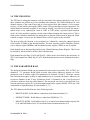
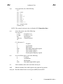
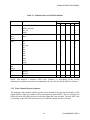
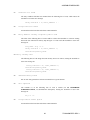
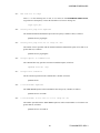
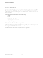
1.1 THE MICROCODE CONTROL STORE
The TPU accesses microcode for execution from the microcode control store. The microcode
control store for the predefined functions is the TPU ROM. For your customized functions, the
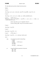
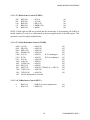
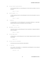
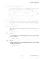
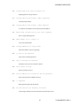
microcode control store is the emulation memory (MCU RAM or flash). Figure 1-1 shows a 2K
byte microcode control store map; other MCUs have 1K bytes for the microcode control store.
This map applies when predefined functions are executed from TPU ROM as well as when your
functions are executed from emulation memory.
The microcode control store consists of two parts: the microcode segments and the entry point
segments.
EQUIVALENT
CPU RAM BYTE
ADDRESS FOR
EMULATION
PURPOSES
MICROCODE
LONGWORD
ADDRESS
LONGWORDS
MICROCODE
$000
$000
$17F
$5FC
FUNCTION 0
ENTRY POINTS
0 15
0, 0 ...
0,1 ...
$180
$600
0, 14
0, 15
$187
$61C
FUNCTION 1
ENTRY POINTS
0 15
1, 0 ...
1, 1 ...
$188
$620
1, 14
1, 15
$18F
$63C
:
:
15, 0 ...
15, 1 ...
$1F8
$7E0
15, 14
15, 15
$1FF
$7FC
FUNCTION 15
ENTRY POINTS
0 15
Microcode Segment
Entry Point Segment
Figure 1-1. Typical Microcode Control Store Memory Map
TPUMASMREF/D REV 3
8
TPU DESCRIPTION
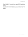
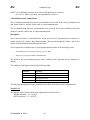
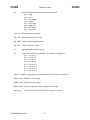
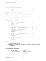
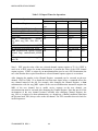
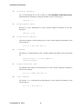
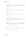
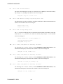
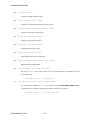
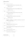
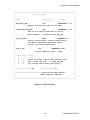
The TPU2 has an extended memory map of 4K or 8K bytes. Figure 1-2 shows a memory map for
a 4K-byte microcontrol store.
LONGWORDS
BANK 0
MICROCODE
MICROCODE
LONGWORD
ADDRESS
EQUIVALENT
CPU RAM, FLASH
BYTE ADDRESS
FOR EMULATION
PURPOSES
$000
$000
FUNCTION 0
ENTRY POINTS
0 15
0, 0 ...
0,1 ...
$180
$600
0, 14
0, 15
$187
$61C
FUNCTION 1
ENTRY POINTS
0 15
1, 0 ...
1, 1 ...
$188
$620
1, 14
1, 15
$18F
$63C
:
:
15, 0 ...
15, 1 ...
$1F8
$7E0
15, 14
15, 15
$1FF
$7FC
$200
$800
$375
$DFC
$380
$E00
$3FF
$FFC
FUNCTION 15
ENTRY POINTS
0 15
BANK 1
MICROCODE
ADDITIONAL
ENTRY POINTS
Microcode Segment
Entry Point Segment
Figure 1-2. Microcode Control Store Memory Map for 4K TPU2
9
TPUMASMREF/D REV 3
TPU DESCRIPTION
1.1.1 Microcode Segments
As Figures 1-1 and 1-2 show, the microcode resides in one or more segments of the control store,
segments not occupied by the entry points. The segments are located in one or more banks on
512-longword boundaries. The microcode consists of 32-bit microinstructions organized in a
hierarchy of state routines and functions. A state routine is an uninterruptible sequence of
microinstructions, such that the sequence executes entirely in one bank, without jumps or calls
across bank boundaries. Each state routine has a 9-bit longword address; in the TPU2, each state
routine also has a two-bit bank address. A function consists of as many as 16 state routines.
When an event, which constitutes a request for service, occurs on a channel, the scheduler
considers the priority of the channel and whether the microengine is available to execute the
microcode for the function. When the scheduler determines that the microengine is ready to
execute the function, it performs a task switch to the function. The task switch passes control to
the appropriate state routine and the microinstructions are fetched and executed in sequential
order (unless a branch instruction is executed) until an END subinstruction is executed.
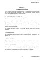
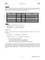
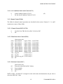
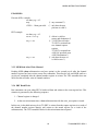
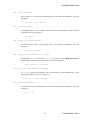
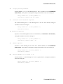
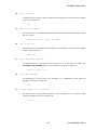
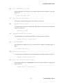
1.1.2 The Entry Point Segment
The entry point segment resides in a contiguous block of the control store located at the top of a
memory bank (the top of memory for TPU1). For TPU2, it is possible to define multiple entry
point segments, each in a different bank. The TPU control register, TPUMCR2, designates the
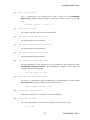
bank number of the entry points to be used at run time. Table 1-1 shows entry-point organization.
The entry point table consists of eight-longword blocks that contain the 16 16-bit entry points for
each function. Figure 1-3 shows the longword-block format for the TPU1. Each block is located
in the entry table according to the function number; the highest function number entry point
block is at the top of the segment. Within each entry block, upon the assertion of a host service
request, the host request bits and the pin state select one of the entry points 03 for the host
control states. One of entry points 4 – 15 for the operational states is selected by the
configuration of the link request bit, the match/transition service request bit, the pin state, and
channel flag 0 when both host request bits are clear and a link, match, or input transition service
request is asserted.
The TPU2 has an extended microcode address space, but the original TPU execution unit is
limited to a 9-bit address range. The TPU2 longword-block format is like that of Figure 1-3,
except for bits 9 and 10, which contain the bank number instead of the value 00. TPU2 selects
the bank in which to execute when the entry point is fetched on a state transition. During the
execution of the state routine, the microcode cannot cross a bank boundary by instruction fetches,
jumps or calls. As most TPU microcode consists of numerous small state routines, the bank
boundary limitation seldom is a problem.
TPUMASMREF/D REV 3
10
TPU DESCRIPTION
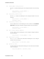
Table 1-1. Entry Points and Channel Conditions
Entry
Points
Host
Control
States
Operational
States
0
1
2
3
4
5
6
7
8
9
10
11
12
13
14
15
Service Request Sources
Channel Conditions
Host
Link
Match/Transition
Pin
Channel
Request Request Service Request
State
Flag 0
(HSR)
(LSR)
(M/TSR)
01
x
x
0
x
01
x
x
1
x
10
x
x
x
x
11
x
x
x
x
00
0
1
0
0
00
0
1
0
1
00
0
1
1
0
00
0
1
1
1
00
1
0
0
0
00
1
0
0
1
00
1
0
1
0
00
1
0
1
1
00
1
1
0
0
00
1
1
0
1
00
1
1
1
0
00
1
1
1
1
Note: The two Host Request (HSR) bits are identified, left to right, as HSR1 and
HSR0.
15
14
PP
13
12
11
M E N PPD
10
9
8
7
Bank
/Preload
6
5
4
3
2
1
State Routine Address
Note: For TPU2, bits 9 and 10 define the state routine bank number. For TPU1, the value %11 in bits 9 and
10 means no pre-load takes place, the value %00 means that P and DIOB are pre-loaded.
Figure 1-3. Entry Point Format
Each entry corresponds to a state and contains:
1. The start address of the state routine.
2. The Preload Parameter number specification (PP).
11
TPUMASMREF/D REV 3
TPU DESCRIPTION
3. The destination of the Preload Parameter (PPD).
0-P
1 - DIOB
4. Next time slot match flag enable (MEN).
0 - disable match recognition latch (MRL) assertion during next time slot
1 - enable MRL assertion during next time slot
Note: If the condition for a match exists, then MRL may be asserted after the time slot.
When a time slot transition occurs, the specified Preload Parameter is loaded into the specified
destination (P register or DIOB register), and the µPC is loaded with the address of the state
routine.
1.2 THE MICROENGINE
The microengine fetches and decodes the microinstructions of a state. It directs operations of the
execution unit and the timer channels and processes conditional branches using its branch PLA.
Direct and indirect addressing modes are provided by the microengine for addressing parameters
in the parameter RAM. Direct addressing modes can be either absolute or relative. Absolute
addressing uses the operand as the address. Relative addressing uses the operand in an
arithmetical relation to the channel number. Relative addressing is very useful in designing
microinstruction sequences that can be executed on any channel.
The microengine provides overlap fetching of the next microinstruction (pipelining). The
microengine fetches a microinstruction while the previous microinstruction is executed,
providing a pipeline length of one. The microinstruction following a branch or jump
microinstruction can be executed prior to the branch or jump, or can be flushed without being
executed. That is, the fetched microinstruction in the pipeline can be replaced with a NOP
microinstruction, which is generated according to conditions valid at the time of execution.
1.3 THE EXECUTION UNIT
The execution unit (EU) consists of a number of registers, functional units, and data paths. These
elements evaluate and control the channel resources to synthesize time functions, under control
of the microengine. The EU accesses the match and capture registers, the timer counter registers
(TCR1 and TCR2), the channel number register, the link logic, and the parameter RAM. The EU
contains:
TPUMASMREF/D REV 3
12
TPU DESCRIPTION
•
The arithmetic unit (AU)
•
A 16-bit shifter through which the result of the AU is passed and optionally shifted by
one
•
A 16-bit shift register (SR)
•
A 16-bit accumulator register (A)
•
A 16-bit preload register (P)
•
A 16-bit input/output buffer (DIOB)
•
A 16-bit Event Register Temporary register (ERT)
•
A 4-bit Decrementor (DEC)
•
A 4-bit Channel number register (CHAN_REG)
•
A 4-bit encoded link register (LINK)
The microcycle, which times the microengine and consists of timing states T1, T2, T3, and T4
(during two CPU clocks), is the basic timing unit for the EU. During a microcycle of an AU
operation, the EU performs the following operations:
•
In state T1, load one or two operands from various registers onto the two internal buses.
•
In state T2, add or subtract the operands, in the arithmetic unit (AU), and generate one
result.
•
In state T3, pass the result through the shifter unshifted, or shift or rotate the result in the
shifter and return the shifted result on one of the internal buses into a destination register.
•
In state T4, write the result into a register or into parameter RAM.
Timing states T1 – T4 time other operations similarly.
The A bus and the B bus, internal EU buses, transfer data between the registers and the
functional units. These buses transfer the operands into the AU. The A bus can read accumulator
A, the P register, the DIOB buffer, timer counter registers TCR1 and TCR2, the ERT register,
decrementor DEC, and the CHAN_REG register. The A bus can write the P register, accumulator
A, the DIOB buffer, timer counter registers TCR1 and TCR2, the ERT register, the LINK
register, the CHAN_REG, and decrementor DEC. The B bus can read the read shift register SR,
accumulator A, the P register, and the DIOB buffer.
13
TPUMASMREF/D REV 3
TPU DESCRIPTION
1.4 THE CHANNELS
The TPU has 16 orthogonal channels, each one associated with a timing signal (pin). Any one of
these channels can perform any of the standard time functions. The control hardware for each
channel consists of pin control logic and an event register block that contains a 16-bit capture
register, a 16-bit match event register (MER), and a 16-bit greater-than-or-equal comparator. The
control hardware normally responds to an event by driving a specified level on the pin when a
match occurs, or by capturing the count in TCR1 or TCR2 when a specified input transition
occurs. It is also possible to generate a match event without changing the output pin level. This is
often used to extend the duration of an output pulse or generate a timeout on an input pin. When
a match or capture event occurs, the channel issues a service request to the scheduler.
The host specifies the function to be performed in a channel by setting the channel function
select register (CFSRn) to the function number. The host sequence register (HSQRn), the host
service request register (HSRRn), and the channel priority register (CPRn) are set as required.
Each channel has an Interrupt Request Bit in the Channel Interrupt Status Register. This bit can
be asserted by the microcode with the CHAN subinstruction.
Each channel has two flags, FLAG0 and FLAG1, which can be set/cleared by the microcode. In
TPU2 each channel has a third flag, FLAG2. Branch subinstructions can be conditioned on these
flags.
1.5 THE PARAMETER RAM
The dual port parameter RAM can pass parameters between the host and the TPU. In TPU1, for
channels 0 - 13, parameter RAM (when accessed with relative addresses) includes six 16-bit
parameters each; it includes eight 16-bit parameters for channels 14 and 15. Therefore, custom
time functions that require as many as eight parameters to be accessed with relative addresses can
execute on channels 14 and 15 only. (Parameters 6 and 7 of channels 14 and 15 can be accessed
with direct addresses from any other channel.) The microcode can read or write the RAM to or
from the parameter register (P), or the data input/output buffer register (DIOB). TPU2 has a full
complement of eight parameters for each channel, 0 - 15.
The TPU addresses the RAM in one of the following modes :
•
DIRECT MODE - RAM address is taken from microinstruction bits(8:2)
•
INDIRECT MODE - RAM address is taken from DIOB bits (7:1)
•
RELATIVE MODE - RAM address bits (6:3) are taken from channel number register bits
(3:0) and RAM address bits (2:0) are taken from microinstruction bits (4:2).
TPUMASMREF/D REV 3
14
TPU DESCRIPTION
When both the TPU and the host access the RAM at the same time, if the TPU loses arbitration, a
wait state is generated. This wait state freezes the µPC, but the whole access is transparent to the
microcode.
Both the host and the TPU can access parameter RAM. The host can read or write a 32-bit word,
but the channel access is 16 bits. To prevent coherency problems, consecutive read or write
operations to a parameter by the channel are protected from interruption by host read or write
operations.
15
TPUMASMREF/D REV 3
TPU DESCRIPTION
TPUMASMREF/D REV 3
16
ASSEMBLY LANGUAGE
CHAPTER 2
ASSEMBLY LANGUAGE
A TPU assembly language has been defined to assist in the development of microcode for the
TPU. The TPU assembler, that executes on an IBM PC or compatible, assembles microcode
from a source program written in TPU assembly language.
2.1 EXECUTING THE ASSEMBLER
The syntax to call the assembler from the command line is:
tpumasm <filename.ext> [<options>]
The default source file extension is .asc. The assembler creates a listing file with the same
filename and the extension .lst, and an object file with the same filename and the extension .s19.
Two additional output files, with extensions .tab and .sym, are created to support the TPU
debugger source level debug mode.
The command line options, which can be used in any order, are described in the following
paragraphs.
2.1.1 Option /NOLIST
The /nolist command line option inhibits writing the assembler listing file. The default is to write
the listing file.
2.1.2 Option /NOSREC
The /nosrec command line option inhibits writing the S-record object file. The default is to write
the S-record file.
2.1.3 Option /SRECWIDTH <n>
The /srecwidth command line option specifies the length of the S-records in the object file. Value
<n> is a decimal number, an even number, specifying the S-record length in ASCII characters.
The minimum is 14, and the maximum is 80. The default length is 66 characters.
17
TPUMASMREF/D REV 3
ASSEMBLY LANGUAGE
2.1.4 Option /SRECTYPE <n>
The /srectype command line option defines the type of the S-records used for object code in the
file created in the object file. Value <n> is 1, 2 or 3. S-record type 1 contains a two-byte load
address. S-record type 2 contains a 3-byte load address. S-record type 3 contains a 4-byte load
address. The default is 1, for S1 records. Appendix C describes the S-record types.
2.1.5 Option /SRECBASE <n>
The /srecbase command line option defines the load address for the S-record files. The range is
0..$FFFFFFFE; the default is 0.
2.1.6 Option /PAGELENGTH <n>
The /pagelength command line option defines the number of lines per page in the listing file. The
range is 0..255; the default is 58 lines.
2.1.7 Option /NOTABLES
The /notables command line option omits the entry table map, the ROM map, the symbol table,
and the macro table from the listing file. This option also inhibits creation of the TPU debugger
files. The default is to include these tables.
2.1.8 Option /HALT
The /halt command line option causes the assembler to halt when the first error is detected. The
error that halted the assembly is displayed on the console screen. This option may inhibit writing
of the listing file or may result in a truncated listing file.
2.1.9 Option /MAXERRORS <n>
The /maxerrors command line option specifies the maximum number of detected errors. The
range of value <n> is 1 ..32767. The default number is 100 errors. TPUMASM halts when the
maximum number of errors has been detected.
TPUMASMREF/D REV 3
18
ASSEMBLY LANGUAGE
2.2 SYNTAX
The TPU assembly language is a free format assembly language. A new line character (line feed
and carriage return) marks the end of a line. A statement consists of one assembler directive or
one microinstruction (one ROM line), terminated with a period. The keyword of a subinstruction
may be placed anywhere on a line, any number of spaces or tabs may be used at any point on a
line, and a statement may extend beyond the end of a line. Limitations apply to %INCLUDE and
%MACRO directives (see descriptions in 2.3 ASSEMBLER DIRECTIVES). Assembly
language statements are case insensitive; that is, all statements are translated into upper case. The
maximum line length is 118 characters.
2.2.1 Notation
In the syntax description the following notation is used:
• Optional items are enclosed within braces - {optional}.
• Assembler directives start with a percent (%) character.
• Names in italics refer to categories of items and are neither used nor recognized by
the assembler.
• The exclamation point (!) indicates the inverse (ones complement) of the value.
• The vertical line (|) means OR.
• The asterisk (*) means the current address.
2.2.2 Comments
A comment resembles the Pascal comment and has the following form:
(* this is a comment *)
or
{ this is another comment }
A comment can be written anywhere in the code and on any number of lines. The assembler
ignores comments except to write them to the listing file. Comments can be nested if both
delimiters are used: one delimiter enclosing the entire comment, and the other enclosing the
nested comments. Comment delimiters can be used to make one or more lines of a program into
a comment. If the enclosed lines already contain comments, use the alternate delimiter to delimit
the entire comment.
19
TPUMASMREF/D REV 3
ASSEMBLY LANGUAGE
2.2.3 Immediate Data
Immediate data in AU subinstructions has the following form:
#number
#$number
#%number
Decimal number
Hexadecimal number
Binary number
(ex. #202 )
(ex. #$F5 )
(ex. #%100101)
2.2.4 Numeric Addresses
Numeric addresses. such as absolute RAM addresses, have the following form:
number
$number
Decimal number
Hexadecimal number
(ex. 1024 )
(ex. $34FE)
2.2.4 Identifiers
An identifier is a sequence of characters starting with a letter and containing letters, digits,
backslashes (\) or underscores (_). Identifiers are used as macro names and labels. An identifier
example is as follows:
IDENTIFIER_1
When a label is defined, the label must be followed by a colon (:). A label may consist of as
many as 40 characters; the first 20 characters must be unique with respect to the first 20
characters of other labels. A label example is as follows:
sum:
goto sum
nop
.
.
.
au a:=1.
TPUMASMREF/D REV 3
20
ASSEMBLY LANGUAGE
2.2.5 Microinstructions
A microinstruction has the following form:
{label: } subinstruction1{; subinstruction2; subinstruction3...}.
Each microinstruction corresponds to one line (32-bit longword) of microcode. Each
subinstruction consists of a group of fields relating to a TPU resource (microengine, RAM,
channel, atithmetic unit).
A subinstruction has the following form:
keyword field1{, field2, field3...}
No two subinstructions of a microinstruction may have the same keyword; that is, the keywords
of the subinstructions in a microinstruction must be unique.
2.2.6 Macros
The TPU assembler supports macros, which substitute strings for the macro names. The
%MACRO directive defines a macro. When the macro name preceded by a commercial at (@)
sign is used in a source code statement, the assembler substitutes the string from the %MACRO
directive for the macro name in the statement. See the %MACRO directive for details.
2.3 ASSEMBLER DIRECTIVES
This section describes the assembler directives, which direct the assembler with respect to its
processing of the source file. A directive always begins with a percent ("%") character. The
assembler recognizes six directives: %entry, %include, %macro, %org, %page, and %type.
EXAMPLE:
%macro count 'prm0'. %macro count1 'prm1'.
21
TPUMASMREF/D REV 3
%ENTRY
Define Entry
%ENTRY
The %ENTRY directive defines one or more entries in the entry table.
Syntax:
%entry {function = 0..15 | $0..$F;} {name = identifier;} start_address {bank_no,} label | *;
{enable_match (default) | disable_match;} cond hsr0=0|1, hsr1=0|1, lsr=val, m/tsr=val, pin=val,
flag0=val {; ram_reg <- pp_spec} {;bank=bank_no {,bank-no}} .
where:
val
is 0 | 1 | x
ram_reg is p | diob
bank_no is 0 | 1 | 2 | 3 (*TPU2 only, depending on control memory size.*)
pp_spec is prm0 | prm1 | prm2 | prm3 | prm4 | prm5 | prm6 | prm7
(* prm6 and prm7 are valid only for the TPU2*)
The %entry directive defines entries in the entry table. The entry address is defined by the
function number and the conditions listed following keyword cond, which specify the entry
number. The function number may be omitted when the file that contains the %entry directive is
specified in an %include directive that specifies the function number (See %INCLUDE
Directive).
The conditions listed following keyword cond (as well as other subfields) can be listed in any
order. The conditions are:
hsr0
Host Service Request bit 0
hsr1
Host Service Request bit 1
lsr Link Service Request
m/tsr
Match/transition
pin
Pin state
flag0
Channel flag0
NOTES:
(1) If val is don't care (x), then its corresponding argument field may be omitted.
(2) Multiple entries can be defined in a single entry directive by using don't care
values.
The ram_reg field specifies which register, p or diob, is loaded with the preload parameter
specified in the pp_spec field.
TPUMASMREF/D REV 3
22
%ENTRY
Define Entry
%ENTRY
The start_address field specifies the address of the state routine corresponding to this entry. The
asterisk (*) denotes the current address. For TPU2, the bank number of the address may specify a
start address not in the current bank. If you use a label for the start address, but omit the bank
number, the assembler uses the bank number of the label. If the label is not in the current bank,
the assembler searches the other banks, in ascending order. If the assembler finds the label in
another bank, it issues warning number 507; if the assembler does not find the label at all, it
issues error message 47.
The match_enable field specifies whether the match recognition latch (MRL) flag is asserted
during the time slot if the match event occurs. Enable_match allows assertion of MRL.
Disable_match disables assertion of MRL during the current state. After completing the state,
MRL may be asserted. The default is enable_match.
The name field specifies the textual name assigned to the entry in the entry table of the listing
file. If multiple entries are specified in the cond field, all the entries have the same name. The
name field serves no functional purpose and is chiefly used as a cross reference aid for the
programmer. The default name is the encoding of the cond field:
hsr1,hsr0,m/tsr,lsr,pin,flag0.
The bank field specifies the TPU2 bank into which the current entry is to be assembled. Note that
the expression can take multiple arguements, so it is possible to build alternate entry point tables.
If the bank expression is omitted, then bank 0 is the default.
EXAMPLE:
%entry function = 3; name = host_service; start_address PP5; enable_match; cond hsr1=0,
hsr0=1, lsr=x, m/tsr=x, pin=x, flag0=x;
ram diob <- prm5.
(* entries 0 and 1 of function 3 are defined. (hsr1=0 hsr0=1 are expanded to 01xx0x and
01xx1x.) On channel transition diob is loaded by parameter 5; match is enabled during
the state. The state starts at label PP5. Function and entry point in bank 0 or TPU1
specified. *)
23
TPUMASMREF/D REV 3
%INCLUDE
Include File
%INCLUDE
The %INCLUDE directive includes a file in the source file, replacing the directive.
Syntax:
%include 'path' {; function= 0..15 | $0..$F} {; bank=0 | 1 | 2 | 3 }.
(Note: The bank= syntax is valid only for the TPU2.)
The file specified by 'path' is included in the source file. If specified, the number that follows
keyword function is passed to the included file as the function number. For the TPU2, if the
directive includes the bank number, the function is assembled in the specified bank. This
provides a limited degree of modular assembly. If the included file already contains a function
number or bank number specification, the TPU ignores such numbers in the %include directive.
No other directive, microinstruction or subinstruction (only a comment) can be on the same line
with an %INCLUDE directive.
EXAMPLES:
%include 'PSP.SRC'; function = 9.
%include 'SM'.
NOTES: (1) If the source code contains more than one %include directive for the same file
name, the assembler ignores the second and subsequent directives and issues a
warning message at the end of the assembly.
(2) %include directives can be nested; i.e. a source file can include a file which
includes another file.
TPUMASMREF/D REV 3
24
%MACRO
Macro Definition
%MACRO
The %MACRO directive defines a macro.
Syntax:
%macro macro_name 'macro_value'.
where:
macro_name
is an identifier.
macro_value
is any string that does not contain a newline (carriage return and line feed).
Macro macro_name is defined. Reference the macro by writing the macro name preceded by the
commercial at ("@") character in a statement of the source file.
EXAMPLE:
Macro definition:
%macro aa 'prm0'.
Macro call:
ram p <- @aa.
25
TPUMASMREF/D REV 3
%ORG
Set Location Counter
%ORG
The %ORG directive sets the location counter, which contains the current address.
Syntax:
%org org_exp.
where:
org_exp is { 0 | 1 | 2 | 3,} address | * | label
The %org directive is used to change the current address. The asterisk (*) denotes a special
variable, the current address. The range of values is 0..511 for tpu1_size of 512 or 0..255 for
tpu1_size of 256 as specified in the %type directive. For tpu2_size of 1024, the range of address
values is 0..511, and the bank may be specified as 0 or 1. For tpu2_size of 2048, the range of
address values is 0..511, and the bank may be specified as 0..3.
EXAMPLE:
%org $50.
(* assigns the current address to 50 hex *)
%org 1,0.
(* assigns the current address to the first address of the second bank *)
TPUMASMREF/D REV 3
26
%PAGE
Eject Page
%PAGE
The %PAGE directive ejects a page of the listing, which effectively begins a new page.
Syntax:
%page.
EXAMPLE:
%page.
27
TPUMASMREF/D REV 3
%TYPE
TPU Type
%TYPE
The %TYPE directive specifies the type of the TPU for which microcode is to be assembled, and
the size of the microcode area in the control store of the TPU.
Syntax:
%type tpu1, tpu1_size | tpu2, tpu2_size .
where:
tpu1_size is 256 | 512
tpu2_size is 512 | 1024 | 2048
The %type directive specifies the target TPU as tpu1 or tpu2, plus an available size for the
microcode area of control store. The %type directive is required; it must be the first statement in
the source file.
EXAMPLE:
%type tpu1, 512.
TPUMASMREF/D REV 3
28
ASSEMBLY LANGUAGE
2.4 ASSEMBLER SUBINSTRUCTIONS
Each line of microcode is a microinstruction. The TPU assembler defines subinstructions that
cause the assembler to assemble specified values in certain fields of a microinstruction. The
subinstructions correspond approximately to the operation categories of the TPU shown in
Figure 3-1. A microinstruction consists of one or more subinstructions, in one of the formats
shown in Figure 3-1. Which format a microinstruction uses is determined by the subinstructions
specified in the microinstruction, each of which implies certain microinstruction fields. Certain
combinations of subinstructions and fields are invalid because none of the five formats includes
the combination of fields implied by the subinstructions. Table 3-1 relates the microinstruction
fields and the subinstructions.
29
TPUMASMREF/D REV 3
AU
Arithmetic Unit
AU
The au subinstruction performs arithmetic and shifting operations. Operands are provided on the
A bus and the B bus, and the result is placed on the A bus.
Syntax:
au adst op (const | expr) {,ccl} {,shift} {,read_mer}
where:
adst
is A bus destination, one of the following:
a
Accumulator
sr
Shift register
ert
Event register temporary
diob
Data input/output buffer register
p_high
P register, bits 15..8
p_low
P register, bits 7..0
p
P register (16 bits)
link
Link register
chan_reg
Channel register
dec
Decrementor
chan_dec
Concatenation of the channel register and decrementor.
tcr1
Time counter register 1
tcr2
Time counter register 2
nil
op
is operator, one of the following:
:=
Assignment
:=>>
Assignment and shift right
:=<<
Assignment and shift left
:=R>
Assignment and rotate right
const
is constant, one of the following:
0
1
max
$FFFF
!0
$8000
NOTE : max is the constant 8000 (hex).
TPUMASMREF/D REV 3
30
AU
AU
Arithmetic Unit
expr
is an expression, one of the following:
asrc
asrc + const
asrc - 1
asrc + bsrc
asrc + bsrc + 1
asrc - bsrc
asrc - bsrc - 1
asrc + !bsrc
asrc + !bsrc + 1
asrc + #immed_data
#immed_data
NOTE : The syntax for #immed_data is defined in 2.2.3 Immediate Data.
asrc
is an A bus source, one of the following:
8 or fewer bits
p_low
P register (7..0)
p_high
P register (15..8)
dec
Decrementor
chan_reg
Channel Register
#0
(* 16-bit source *)
p
a
sr
diob
tcr1
tcr2
ert
P register
Accumulator
Shift register
Data input/output buffer register
Time counter register 1
Time counter register 2
Event register temporary register
bsrc
is a 16-bit B bus source, one of the following:
p
P register
a
Accumulator
sr
Shift register
diob
Data input/output buffer register
ccl
Latch condition codes at the end of the microcycle.
shift
Shift the contents of the shift register to the right one bit position.
read_mer Read the channel match event register (MER) into the ERT.
31
TPUMASMREF/D REV 3
AU
Arithmetic Unit
AU
NOTE: (1) A shift right operation and a write to SR operation are exclusive.
(2) An asrc source and a read_mer operation are exclusive
Valid Subinstruction Combinations
The au subinstruction that does not use an immediate value on the B bus can be combined with
ram, chan (format 2), and dec_return, end, or repeat subinstructions.
The au subinstruction that uses an immediate value on the B bus can be combined with chan
(format 5) and dec_return, end, or repeat subinstructions.
Description
The au has two sources: A bus and B bus. At the start of the AU operation the two sources are
loaded into the AU latches, then added together, then passed through the shifter, and at last
written to the destination specified using the A bus.
An au operation is considered to be a word operation unless either of the following is true:
•
The destination is a byte of the P register (p_low or p_high).
•
The asrc is a byte register added to immediate data.
The result of the au operation generates some condition code flags that can be latched (ccl
option).
The condition code flags are listed in the following table.
Condition
N
C
Z
V
Meaning
AU result is negative
Carry
AU result is zero
Overflow
The following paragraphs describe generation of the flags for both byte and word operations.
Negative (N)
The negative flag is asserted if the most significant bit of the result is 1
WORD operation : N := AU(15)
BYTE operation : N := AU(07)
TPUMASMREF/D REV 3
32
AU
AU
Arithmetic Unit
Carry (C)
When the shifter does not shift, the carry flag is the carry out of the result in add operations, and
borrow in subtract operations. A subtract operation is addition with the B operand inverted. The
carry out is taken from a different bit in byte and word operations.
Shifter
Not Shifting (:=)
Operation
ADD
Length
Word
Byte
SUBTRACT Word
Byte
Shift Right (:=>>)
Rotate Right (:=R>)
Shift Left (:=<<)
Carry Flag
carry out from AU(15)
carry out from AU(07)
carry out from AU(15) invert
carry out from AU(07) invert
AU(00) (AU result lsb)
AU(00) (AU result lsb)
AU(15) (AU result msb)
Zero (Z)
The ZERO flag is asserted if the result equals zero.
WORD operation : Z := (AU(15:00) = 0000 hex)
BYTE operation : Z := (AU(07:00) = 00 hex)
Overflow (V)
Overflow is generated when the result, using signed numbers, is outside the AU range. The
definition is:
ADD operation : V := ( Am•Bm•!Rm + !Am•!Bm•Rm)
SUBTRACT operation : V := ( Am•!Bm•!Rm + !Am•Bm•Rm)
where: Rm - Result operand - MSB
Am - A-Bus source operand - MSB ( A-Bus MSB )
Bm - B-Bus source operand - MSB ( B-Bus MSB )
MSB is bit 7 for BYTE operation, and bit 15 for WORD operation.
The shift register residing in the Execution Unit (EU) can also be loaded with the result shifted
one bit to the right. A special case is when both the shift register and a right shift of the AU result
are specified; in this case the upper bit of the AU result is shifted to the least significant bit of the
shift register. This configuration is a 32-bit shifter. The shift register is referenced in the shift
field.
33
TPUMASMREF/D REV 3
AU
AU
Arithmetic Unit
Two microinstruction fields, B bus invert (BINV) and carry in (CIN), are controlled by the
microcode. BINV is asserted in subtract operations. CIN is asserted in any of the following
cases:
1. A subtract operation is specified (ex. a := a - p; ).
2. The 1 constant is specified (ex. a := a + 1; ). (* Notice no pound sign (#) *)
3. The max constant is specified (ex. a := tcr1 + max).
Keyword ccl controls the latch of the condition code at the end of the microinstruction cycle. If
ccl is specified the condition code is latched, otherwise no latch is executed.
AU shifter and shift register word results:
SR
AU
CFLAG
:=
Cout 15
0
15
SR
AU
CFLAG
:=,shft
0
Cout 15
0
15
0
15
0
15
0
15
0
SR
AU
CFLAG
:=<<,shft
0
0
AU
15
0
SR
CFLAG
0
15
0
15
CFLAG
AU
:=>>,shft
0
SR
AU
CFLAG
:=<<
:=>>
0
0
SR
0
15
0
AU
15
0
SR
CFLAG
:=R>
15
0
AU
0
SR
CFLAG
:=R>,shft
0
15
TPUMASMREF/D REV 3
15
0
34
15
0
AU
AU
Arithmetic Unit
A bus source registers that do not require the full 16 bits of the A bus, and the bits they occupy
on the bus, are listed in the following table:
p_low
p_high
dec
chan_reg
mer
0
AB(7:0) := P(7:0), AB(8:15) :=0
AB(7:0) := P(15:8), AB(8:15) :=0
AB(3:0) := DEC(3:0); AB(4:15) :=0
AB(7:4) := CHAN(3:0); AB(0:3),AB(8:15) :=0
ERT(15:0) := MATCH REGISTER(15:0)
AB(15:0) := 0000
B bus source registers that do not require the full 16 bits of the B bus, and the bits they occupy
on the bus, are listed in the following table.
immediate_data
0
BB(7:0) := INSTRUCTION(16:9); BB(15:8) := 0
BB(15:0) := 0000
NOTE: If shift right and SR are specified and the decrementor is decrementing then the B bus is
loaded with the B bus source if the least significant bit of the shift register is 1, or 0, if
the least significant bit of the shift register is 0. This operation supports the use of the
shift register in multiply operations described in B.1 MULTIPLY.
The following table lists the AU destinations that do not require 16 bits, and the A bus bits these
destinations occupy.
p_high
p_low
link
chan_reg
dec
chan_dec
nil
P(15:8) := AB(7:0)
P(7:0) := AB(7:0)
Link(3:0) := AB(7:4)
CHAN(3:0) := AB(7:4)
DEC(3:0) := AB(3:0)
DEC(3:0) := AB(3:0); CHAN(3:0) := AB(7:4)
no destination
Keyword read_mer specifies that the match event register is to be read into the ERT. This
operation is done on T2 of the µcycle, and is only possible when no A bus source is specified in
the au subinstruction.
35
TPUMASMREF/D REV 3
AU
Arithmetic Unit
AU
EXAMPLES:
au a := 1.
(* assign 1 to a *)
au ert := p + 1.
(* ert gets the value of p incremented by 1 *)
au p := max.
(* p gets the constant #$8000 *)
au a :=>> p.
(* a gets the value of p shifted right*)
au a :=<< !p.
(* a gets the value of !p shifted left*)
au diob := p + !diob + 1.
(* p gets the value of p plus the value of !diob plus 1
*)
au diob := p - diob.
(* the same as above example *)
au diob :=>R diob - 1.
(* diob is decremented by 1 rotated right *)
au sr := #$55.
(* sr gets the value 55 hex *)
au sr := a + #%1101.
au a := p + 1, shift.
(* sr gets the value of a plus 13 *)
(* a gets the value of p incremented by 1 and the shift
register is shifted right *)
au diob := a, shift, ccl, read_mer.
TPUMASMREF/D REV 3
(* diob gets the value of a, the shift register is shifted
right, mer is read to the ert, the condition codes
resulting from the arithmetic operation are latched.
*)
36
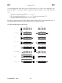
CALL
CALL
Call Subroutine
The call subinstruction provides a branch to subroutine operation.
Syntax:
call label {, flush | no_flush}
where:
label
is an identifier
Valid Subinstruction Combinations
The call subinstruction can be combined with chan (format 4), ram, and dec_return, or repeat
subinstructions.
Description
If no option or the no_flush option is specified, the return address register (invisible to the
programmer) is loaded with the new value for the µPC and the µPC is loaded with the address
specified in the label field. If the flush option is specified, the return address register is loaded
with the current address + 1; otherwise, the return address register is loaded with current address
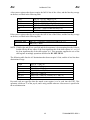
+ 2, as shown in Figure 2-1. The single return address register can store only one return address;
subroutines cannot be nested.
EXAMPLE:
L1:
L2:
call SUB1, flush.
au a := 1.
(* jump to SUB1, don't execute next
command, Return address is L2. *)
37
TPUMASMREF/D REV 3
CALL
CALL
Call Subroutine
CALL
, flush
CALL
, no_flush
Inst A
NOP
Subroutine
Subroutine
Inst B
Inst A
Inst B
Figure 2-1. Subroutine Calls
TPUMASMREF/D REV 3
38
CHAN
CHAN
Channel Control
The chan subinstruction performs channel control operations.
Syntax:
Format 2
chan {flags}{, pac}{, psc}{, write_mer}{, neg_TDL}{, neg_MRL}{, neg_LSL}{, cir}
Format 3
chan {flags} {, tbs} {, pac}{, psc}{, config := p}{, enable_mtsr|disable_mtsr}
Format 3
(* TPU2 syntax. *)
chan {flags} {, tbs} | {{, neg_MRL} {, neg_TDL}} {{, pac}{, psc}} | {, config := p}
{, enable_mtsr|disable_mtsr}
(* Note config and pac or psc are mutually exclusive*)
(* Note tbs and neg_MRL or neg_TDL are mutually exclusive*)
Format 4
chan {flags} {, neg_LSL}
Format 5
chan {flags} {, neg_LSL} {, cir}
Format 5
(* TPU2 syntax. *)
chan {flags} {, neg_LSL} {, cir} {, match_gte | match_equal }
where:
flags
is one of these keywords for channel flags:
set flag0
set flag1
set flag2
(* TPU2 only *)
clear flag0
clear flag1
clear flag2 (* TPU2 only *)
psc
is one of the following expressions for pin state:
PIN := high
PIN := low
PIN := PAC
39
TPUMASMREF/D REV 3
CHAN
pac
Channel Control
is one of the following expressions for pin control:
pac := high
pac := low
pac := no_change
pac := toggle
pac := low_high
pac := high_low
pac := no_detect
pac := any_trans
write_mer Write match event register
neg_TDL Negate transition detect latch
neg_MRL Negate match recognition latch
neg_LSL Negate link service latch
cir
Assert channel interrupt request
tbs
is one of the following expressions for channel configuration:
tbs := in_m1_c1
tbs := in_m1_c2
tbs := in_m2_c1
tbs := in_m2_c2
tbs := out_m1_c1
tbs := out_m1_c2
tbs := out_m2_c1
tbs := out_m2_c2
config := p Enable configuration of channel control latches from P register 8..0
enable_mtsr
Enable service request
disable_mtsr Disable service request
match_equal Sets the match on a TPU2 channel to equal only
match_gte
Sets the match on a TPU2 channel to greater or equal
TPUMASMREF/D REV 3
40
CHAN
CHAN
CHAN
Channel Control
Valid Subinstruction Combinations
The chan (format 2) subinstruction can be combined with au (B bus not immediate), and
dec_return, end, or repeat subinstructions.
The chan (format 3) subinstruction can be combined with the if subinstruction.
The chan (format 4) subinstruction can be combined with ram, goto or return, and dec_return or
repeat (but not end) subinstructions.
The chan (format 5) subinstruction can be combined with au (B bus immediate), and dec_return,
end, or repeat subinstructions.
Description
A chan subinstruction can be one of several formats; each format consists of a different
combination of channel subinstruction fields. The fields are:
FLAGS
The two flags (for TPU2, three flags) associated with each channel can
be set or cleared. This subinstruction sets or clears the specified flag.
Only one flag operation can be executed per microinstruction.
NEG_TDL
Negate Transition Detect Latch. Executed at the next microcycle.
NEG_MRL
Negate Match Detect Latch. Executed at the next microcycle.
NEG_LSL
Negate Link Service Latch.
WRITE_MER
Write Event register from ert at the next microinstruction cycle.
NOTE: ert must be loaded with valid time prior to write.
PSC
Force the channel pin :
PIN := low
Force pin to low
PIN := high Force pin to high
PIN := PAC Force pin as specified in the pin control latch
ENABLE_MTSR Enable service request
DISABLE_MTSR Disable service request
MATCH_EQUAL Sets the match on TPU2 channels to equal only
MATCH_GTE
Sets the match on TPU2 channels to greater or equal
41
TPUMASMREF/D REV 3
CHAN
Channel Control
PAC
CHAN
Controls the pin action control latches:
PIN configured as output:
high
On match event force pin to high
low
On match event force pin to low
toggle
On match event force pin to toggle
no_change On match event do not change pin state
PIN is configured as input
no_detect
No transition is detected
low_high
Low to high transition is detected
high_low
High to low transition is detected
any_trans
Any transition is detected
TBS
Controls the channel configuration: input/output, match TCR, and
capture TCR.
in_m1_c1
Input channel; capture TCR1; match TCR1
in_m2_c1
Input channel; capture TCR1; match TCR2
in_m1_c2
Input channel; capture TCR2; match TCR1
in_m2_c2
Input channel; capture TCR2; match TCR2
out_m1_c1
Output channel; capture TCR1; match TCR1
out_m2_c1
Output channel; capture TCR1; match TCR2
out_m1_c2
Output channel; capture TCR2; match TCR1
out_m2_c2
Output channel; capture TCR2; match TCR2
CIR
This command asserts the host interrupt request bit for the current
channel.
config := p
Enables the configuration of the channel control latches from P-register
bits(8:0). The psc field (bits 1,0), the pac field (bits 4..2), and the tbs
field (bits 9..5) are loaded.
NOTE: If the P-register is used as the source for channel configuration
then microcode fields tbs, pac, and psc are unused.
EXAMPLES:
chan PIN := high, pac := toggle, neg_TDL.
(* pin value is set to '1', pac is set to toggle, TDL latch is negated. *)
chan tbs := in_m1_c2, pac := low_high.
(* pin is configured as input, on low to high transition or match on TCR1, TCR2 is
captured *)
chan config := p, disable_mtsr.
(* channel is configured by the contents of p register, service requests are disabled.
*)
TPUMASMREF/D REV 3
42
DEC_RETURN
Decrement and Return
DEC_RETURN
The dec_return subinstruction provides a return from subroutine when the count in the
decrementor reaches zero.
Syntax:
dec_return
Valid Subinstruction Combinations
The dec_return subinstruction can be combined with au, chan, ram, and call or goto
subinstructions.
Description
Start decrementing, when decrementor reaches 0, jump to the address pointed to by the return
address register (RAR). If dec_return and call subinstructions are issued in the same
microinstruction, the value of the decrementor specifies the number of commands to be executed
from the sub-routine. If the value of the decrementer is 0, 16 microinstructions are executed.
Refer to 3.2.11 Jump and Decrementor Operations for additional information.
NOTE: After the decrementor reaches 0 it is set to F hexadecimal.
EXAMPLE:
au dec := #5.
call SUB1, flush; dec_return.
(* execute 5 commands from SUB1 and return *)
43
TPUMASMREF/D REV 3
END
End of State
END
The end subinstruction controls the end of state.
Syntax:
end
Valid Subinstruction Combinations
The end subinstruction can be combined with au, chan, and ram subinstructions.
Description
End current state. After the current microinstruction completes, control passes to the hardware
scheduler.
EXAMPLE:
ram p -> prm4; end.
TPUMASMREF/D REV 3
(* p gets parameter 4 of the channel whose number is in channel
number register, and the state ends. *)
44
GOTO
Unconditional Branch
GOTO
The goto subinstruction branches to a specified location.
Syntax:
goto label {, flush | no_flush}
where:
label
is an identifier
Valid Subinstruction Combinations
The goto subinstruction can be combined with chan (format 4) and ram subinstructions.
Description
When no option or the no_flush option is specified, the next microinstruction is executed and the
µPC is loaded with the address specified in the label field. When the flush option is specified, the
next microinstruction is forced to a nop and the µPC is loaded with the address specified in the
label field. The effects of the flush and no_flush options are similar to those shown for the call
subinstruction in Figure 2-1.
EXAMPLE:
goto calc, no_flush.
(* Execute the next microinstruction and branch to the
microinstruction at label calc. *)
45
TPUMASMREF/D REV 3
IF
Conditional Branch
The if subinstruction conditionally branches to a specified location.
Syntax:
if {cond =} {cond_val} then goto label {, flush | no_flush}
where:
cond
is a branch condition, one of the following:
LESS_THAN
LOW_SAME
V
N
C
Z
FLAG2
(* TPU2 only *)
FLAG1
FLAG0
TDL
MRL
LSR
HSQ1
HSQ0
PSL
PIN
(* TPU2 only *)
cond_val is a value, one of the following:
1
0
TRUE
FALSE
label
is an identifier
Valid Subinstruction Combinations
The if subinstruction can be combined with the chan (format 3) subinstruction.
TPUMASMREF/D REV 3
46
IF
IF
Conditional Branch
IF
Description
The condition (cond) is one of the status signals supplied to the branch PLA. The following table
describes each signal:
Condition
N
C
Z
V
LOW_SAME
LESS_THAN
PSL
PIN
LSL
TDL
MRL
FLAG0
FLAG1
FLAG2
HSQ1
HSQ0
TRUE
FALSE
Meaning
AU result is negative (bit 15 = 1)
AU result carry1
AU result is ZERO
OVERFLOW2
(C + Z) asrc is lower/same as bsrc
N*!V + !N*V asrc is less then bsrc
Pin state latch
Pin level3 (* TPU2 only *)
Link Service Latch
Transition Detect Latch
Match Recognition Latch
Channel flag 0
Channel flag 1
Channel flag 2 (* TPU2 only *)
Sequence bit 1
Sequence bit 0
jump always
don't jump
NOTES: 1. Refer to Carry (C) description under au subinstruction.
2. Refer to Overflow (V) description under au subinstruction.
3. Actual state of pin. May be different from PSL.
The cond is optional and if not used a branch always or branch never can be made with (if true
then & if false then).
The condval, TRUE or FALSE, can be used alone.
When no option or the no_flush option is specified and a branch occurs, the next
microinstruction is executed before control passes to the new address. When the flush option is
specified and a branch occurs, the next instruction is forced to nop, and control passes to the new
address. The effects of the flush and no_flush options are similar to those shown for the call
subinstruction in Figure 2-1
EXAMPLE:
if PSL = 1 then goto L5, flush. (* if pin state is 1 then goto L5 and don't execute next
command, else continue to next command. *)
47
TPUMASMREF/D REV 3
NOP
No Operation
The nop subinstruction performs no operation.
Syntax:
nop
Valid Subinstruction Combinations
None.
EXAMPLES:
nop.
TPUMASMREF/D REV 3
48
NOP
RAM
RAM
RAM Operations
The ram subinstruction reads or writes to parameter RAM locations. All operations access 16-bit
words of RAM.
Syntax:
ram ram_reg r/w ram_address
(* TPU1 and TPU2 *)
ram ram_reg <- # [$ | %] 0
(* TPU2 only *)
ram # [$ | %] 0 -> ram_address
(* TPU2 only *)
where:
ram_reg
is a register:
p
diob
r/w
is the operator:
<- read
-> write
ram_address is the RAM address, one of the following:
prm0
prm1
prm2
prm3
prm4
prm5
prm6
prm7
by_diob
even numbers from 0 to 254
[direct address]
(0-15, 0-7)
[direct address] (chan num, param num)
Valid Subinstruction Combinations
The ram subinstruction can be combined with the au (without immediate B bus values), the chan
(format 4), goto or return, and dec_return, end, or repeat subinstructions. However, goto or return
is mutually exclusive with end.
49
TPUMASMREF/D REV 3
RAM
RAM Operations
RAM
Description
The following describe the operands of the subinstruction.
ram_reg
Specifies the register (p or diob) for the subinstruction.
r/w
Specifies the ram operation: read or write.
ram_address The keyword or value used implies the addressing mode, as described in the
following paragraphs.
The addressing modes for parameter RAM are direct, relative, and indirect. A numeric address
implies the direct addressing mode, in which the RAM address is taken from the ram address
field of the microinstruction. This address is an even number in the range of 0..254, or a channel
number (0 - 15) and a parameter number (0-7). (See 3.2.6 RAM Access Coherency and 3.2.7
RAM Parameter for further information about ram accesses).
Keywords prm0..prm7 imply relative addressing. Writing to prm6 or prm7 of channel 0..13 of
TPU1 has no effect; reading these parameters returns 0. The channel number is taken from the
channel register, and the parameter number is taken from the ram address field of the
microinstruction.
Keyword by_diob implies the indirect addressing mode, in which bits 7..1 of diob are used to
address parameter RAM.
NOTE: Two-word coherency is guaranteed by TPU hardware when two consecutive ram
subinstructions access parameter RAM.
EXAMPLES:
ram p <- prm4.
(* p gets parameter 4 of the channel whose number is in channel
number register. *)
ram p -> by_diob.
(* the value of p is written to the ram address denoted by bits 7:1
of diob *)
ram p -> (2,3).
(* the value of p is written to parameter 3 of channel 2 *)
ram diob <- $EC.
(* diob gets the value in ram address EC hex. Important: the ram
absolute address is an even number in the range of 0..FE hex *)
TPUMASMREF/D REV 3
50
REPEAT
REPEAT
Repeat Microinstruction
The repeat subinstruction repeats the microinstruction under control of the decrementor.
Syntax:
repeat
Valid Subinstruction Combinations
The repeat subinstruction can be combined with au, chan (formats 2 and 5), and ram
subinstructions.
Description
The microinstruction is executed the number of times specified in the decrementor + 1. If the
decrementor is set to 0 the command is performed 17 times.
Refer to 3.2.11 Jump and Decrementor Operations for additional information.
NOTE: After the decrementor reaches 0 it is set to F hexadecimal.
EXAMPLES:
au dec := #6.
repeat;
au a := a + p.
(* add the value of p to a *)
(* 7 times *)
51
TPUMASMREF/D REV 3
RETURN
Return from Subroutine
RETURN
The return subinstruction returns control to the address stored in the return address register.
Syntax:
return {, flush | no_flush}
Valid Subinstruction Combinations
The return subinstruction can be combined with the ram subinstruction.
When no option or the no_flush option is specified, the next microinstruction is executed and the
µPC is loaded with the contents of the return address register. When the flush option is specified,
the next instruction is forced to a nop, and the µPC is loaded with the contents of the return
address register. The effects of the flush and no_flush options are similar to those shown for the
call subinstruction in Figure 2-1.
EXAMPLE:
return.
ram p -> prm5.
TPUMASMREF/D REV 3
(* jump to the address in the return address register,
and execute the next microinstruction *)
52
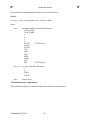
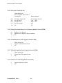
MICRO INSTRUCTION FORMAT
CHAPTER 3
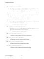
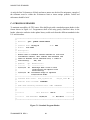
MICROINSTRUCTION FORMAT
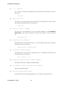
This section describes the microinstruction set. Each of the five formats of microinstructions is
named for the major operations it performs. Each field of a microinstruction format is related to a
TPU resource, and is manipulated by a specific subinstruction. Figure 3-1 shows the
microinstruction formats. The shading corresponds to the operation groups defined in the next
section.
FORMAT 1 : EXECUTION UNIT AND RAM
31 30 29 28 27 26 25 24 23 22 21 20 19 18 17 16 15 14 13 12 11 10
0
0 RW
T1ABS
T3ABD
SHF
S
R
C
C
C
L
C
BI
I
NV
N
T1BBS
9
8
7
6 5
IOM
4
3
2
1
0
DEC/
END
AID (6:0)
FORMAT 2 : EXECUTION UNIT, FLAG, AND CHANNEL CONTROL
31 30 29 28 27 26 25 24 23 22 21 20 19 18 17 16 15 14 13 12 11 10 9
0
E
1 R
W
T1ABS
T3ABD
SHF
T M
D R
L L
C
BI
I
NV
N
T1BBS
8
PAC
7
6 5
L
S
L
PSC
8
7
4
3
2 1
C
I
R
FLC
0
DEC/
END
FORMAT 3 : CONDITIONAL BRANCH, FLAG, AND CHANNEL CONTROL
31 30 29 28 27 26 25 24 23 22 21 20 19 18 17 16 15 14 13 12 11 10 9
1
0
BCC
F
L
S
BAF (8:0)
TBS
B
C
F
PAC
6 5
PSC
4
3
2 1
0
C
C MTSR
M
FLC
BRANCH
FORMAT 4 : JUMP, FLAG, AND RAM
31 30 29 28 27 26 25 24 23 22 21 20 19 18 17 16 15 14 13 12 11 10 9
1
1
0 RW NMA
F
L
S
BAF (8:0)
FLC
L
S
L
8
7
IOM
6 5
4
3
2 1
0
DEC/
END
AID (6:0)
JUMP
FORMAT 5 : EXECUTION UNIT, IMMEDIATE, AND FLAG
31 30 29 28 27 26 25 24 23 22 21 20 19 18 17 16 15 14 13 12 11 10 9
1
1
1
T1ABS
T3ABD
SHF
S C
R C
C L
IIMMEDIATE DATA (7:0)
(T1BBI)
8 7
L
S
L
6 5
EQ/
GE
4 3
FLC
2 1
C
I
R
0
DEC/
END
RAM OPERATIONS
EXECUTION UNIT OPERATIONS
MICROENGINE/SEQUENCING OPERATIONS
CHANNEL CONTROL OPERATIONS
Figure 3-1. Microinstruction Formats
53
TPUMASMREF/D REV 3
MICRO INSTRUCTION FORMAT
3.1 INSTRUCTION FIELDS
This section shows the encoding of the instruction fields referred to in the instruction format and
the timing state in which the field is valid, where applicable. The default of a field (NOP) is a
value of '1', the default value of the ROM.
NOTE: Encodings that are not listed are reserved.
3.1.1 Execution Unit Fields
The fields for execution unit operations are described in this section. Formats 1, 2, and 5 contain
one or more of these fields.
3.1.1.1 T1 A-Bus Source Control (T1ABS)
BYTE Source
0000 AB(7:0)
0001 AB(7:0)
0010 AB(3:0)
0011 AB(7:4)
0111 AB(7:0)
:= P(7:0);
:= P(15:8);
:= DEC(3:0);
:= CHAN(3:0);
:= 00;
SPECIAL OPERATION
0100 AB(15:0)
:= 0;
WORD Source
1000 AB(15:0)
1001 AB(15:0)
1010 AB(15:0)
1011 AB(15:0)
1100 AB(15:0)
1101 AB(15:0)
1110 AB(15:0)
1111 AB(15:0)
AB(8:15) :=0
AB(8:15) :=0
AB(4:15) :=0
AB(0:3),AB(8:15) :=0
AB(8:15) := 0
(t1)
(t1)
(t1)
(t1)
(t1)
ERT := MER;
(t2)
:= P(15:0)
:= A(15:0)
:= SR(15:0)
:= DIOB(15:0)
:= TCR1(15:0)
:= TCR2(15:0)
:= ERT(15:0)
:= 0000
(t1)
(t1)
(t1)
(t1)
(t1)
(t1)
(t1)
(t1)
3.1.1.2 T1 B-Bus Immediate Data (T1BBI)
(8 bits)
x..x
8-bit data field
TPUMASMREF/D REV 3
(t1)
54
MICRO INSTRUCTION FORMAT
3.1.1.3 T1 B-Bus Source Control (T1BBS)
000
001
010
011
111
BB(15:0)
BB(15:0)
BB(15:0)
BB(15:0)
BB(15:0)
:= P(15:0)
:= A(15:0)
:= SR(15:0)
:= DIOB(15:0)
:= 00000
(t1)
(t1)
(t1)
(t1)
(t1)
NOTE: If shift right and SR are specified and the decrementor is decrementing, the B-BUS is
loaded with bsrc (b source) or 0 determined by the least significant bit of the shift register. This
operation is used for register multiplication.
3.1.1.4 T3 A-Bus Destination Control (T3ABD)
0000
0001
0010
0011
0100
0110
0111
1000
1001
1010
1011
1100
1101
1111
A(15:0)
:= AB(15:0)
SR(15:0)
:= AB(15:0)
ERT(15:0)
:= AB(15:0)
DIOB(15:0)
:= AB(15:0)
P(15:8)
:= AB(7:0);
P(7:0) unchanged
P(7:0)
:= AB(7:0);
P(15:8) unchanged
P(15:0)
:= AB(15:0)
Link(3:0)
:= AB(7:4)
CHAN(3:0)
:= AB(7:4)
DEC(3:0)
:= AB(3:0)
DEC(3:0)
:= AB(3:0); CHAN(3:0) := AB(7:4)
TCR1(15:0)
:= AB(15:0)
TCR2(15:0)
:= AB(15:0)
Nil (No destination is selected)
(t3)
(t3)
(t3)
(t3)
(t3)
(t3)
(t3)
(t3)
(t3)
(t3)
(t3)
(t3)
(t3)
3.1.1.5 AU B-Bus Invert Control (BINV)
0
1
Bin(15:0)
Bin(15:0)
:= !BB(15:0) (one's complement)
:= BB(15:0)
55
(t1)
(t1)
TPUMASMREF/D REV 3
MICRO INSTRUCTION FORMAT
3.1.1.6 AU B-Bus Carry Control (CIN)
0
1
Carry in
Carry in
:= 1
:= 0
(t1)
(t1)
NOTE: The creation of the constant 8000(hex) is a special case:
If (T1BBS = 111) & (Cin = 0) & (Binv = 0) then Bin = $8000 (8000 hex)
This is implemented by special logic, inverting bit 15 of Bin to 0.
3.1.1.7 AU Shifter Control (SHF)
00
AB(15:1)
:= AU(14:0), AB(0) := 0;
Carry flag := AU(15)
(shift left)
01
if SRC = 1 THEN
AB(14:0) := AU(15:1),AB(15) := Cout
else
AB(14:0) := AU(15:1),AB(15) := 0
Carry flag := AU(0)
(shift right)
(t3)
(t3)
(t3)
10
AB(14:0)
:= AU(15:1),AB(15) := AU(0)
Carry flag := AU(0)
(rotate right)
(t3)
11
AB(15:0)
:= AU(15:0)
Carry flag := Cout
(no shift)
(t3)
NOTES:
1. Cout is the AU result carry out.
2. In no shift byte operation case, Cout is the carry out from bit 7. Otherwise, Cout is the
carry from bit 15.
3.1.1.8 Shift Register Control (SRC)
0
shift right: SR(14:0)
IF SHF = 01 (shift right)
1
no shift
TPUMASMREF/D REV 3
:=SR(15:1);
then SR(15) :=AU(0)
else SR(15) := 0;
56
MICRO INSTRUCTION FORMAT
3.1.1.9 AU Condition Code Latch Control (CCL)
0
1
Latch Condition Codes (Z,C,N,V)
Do Not Latch Condition Codes (Z,C,N,V)
(t2)
3.1.2 Channel Control Fields
The fields for channel control operations are described in this section. Formats 2, 3, 4, and 5
contain one or more of these fields.
3.1.2.1 Channel Control MUX (CCM)
0
1
Use P(8:5) for TBS, P(4:2) for PAC, P(1:0) for PSC.
Nil
3.1.2.2 Time Base Select Control (TBS)
0000
0001
0010
0011
0100
0101
0110
0111
1101
1011
1001
1111
(Next microcycle)
Input channel;
capture TCR1; match TCR1
Input channel;
capture TCR1; match TCR2
Input channel;
capture TCR2; match TCR1
Input channel;
capture TCR2; match TCR2
Output channel; capture TCR1; match TCR1
Output channel; capture TCR1; match TCR2
Output channel; capture TCR2; match TCR1
Output channel; capture TCR2; match TCR2
neg_mrl
(* TPU2 only *)
neg_tdl
(* TPU2 only *)
neg_mrl, neg_tdl (* TPU2 only *)
nil
3.1.2.3 Pin State Control (PSC)
00
01
10
11
(Next microcycle)
Force pin as specified by PAC latches
Force pin high
Force pin low
Nil
NOTE: If PSC = 00 and PAC is assigned a value in the same microinstruction, the pin value is
set by the NEW PAC value.
57
TPUMASMREF/D REV 3
MICRO INSTRUCTION FORMAT
3.1.2.4 Pin Action Control (PAC)
000
001
010
011
1xx
(Next microcycle)
Pin is OUTPUT Pin is INPUT
on match do:
detect transition:
No change in pin state
Set pin to high
Set pin to low
Set pin to toggle
Nil
No transition detected
Low -> high
High -> low
Any
Nil
3.1.2.5 Match/Transition Detect Service Request Inhibit Control (MTSR)
00
01
1x
Enable Service Request
Inhibit Service Request (Reset condition)
Nil
3.1.2.6 Transition Detect Latch Negation Control (TDL)
0
1
(Next microcycle)
Negate Transition Detect Latch
Nil
3.1.2.7 Match Recognition Latch Negation Control (MRL)
0
1
(Next microcycle)
Negate Match Recognition Latch
Nil
3.1.2.8 Link Service Latch Negation Control (LSL)
0
1
Negate Link Service Latch
Nil
TPUMASMREF/D REV 3
58
MICRO INSTRUCTION FORMAT
3.1.2.9 Flag Control (FLC)
001
000
011
010
100
101
1xx
Set
Clear
Set
Clear
Set
Clear
Nil
Channel Flag0
Channel Flag0
Channel Flag1
Channel Flag1
Channel Flag2 (* TPU2 only *)
Channel Flag2 (* TPU2 only *)
(t1)
(t1)
(t1)
(t1)
(t1)
(t1)
3.1.2.10 Channel Interrupt Request (CIR)
0
1
Assert State Status Bit
Nil
3.1.2.11 Event Register Write Control (ERW)
0
1
(next microcycle)
MER(15:0)
:= ERT(15:0)
Nil
(t2)
3.1.2.12 Match Compare Register Control (EQ/GE)
00
01
11
Assert Match on Greater than or Equal
Assert Match on Equal Only
No Change
(* TPU only *)
3.1.3 RAM Fields
The fields for RAM operations are described in this section. Formats 1 and 4 contain one or more
of these fields.
59
TPUMASMREF/D REV 3
MICRO INSTRUCTION FORMAT
3.1.3.1 RAM Input/Output Mode Control (IOM)
000
P Access Using 3-bit Parameter Number from AID(2:0) concatenated
with Channel number from channel register
000
If RW=0 (Read from RAM) and AID bit 6=1, then Clear P (* TPU2 only *)
001
P Access Using 7-bit Address from DIOB(7:1)
010
P Access Using 7-bit Address from AID(6:0)
100
DIOB Access Using 3-bit Parameter Number from AID(2:0)
concatenated with channel number from channel register
100
If RW=1 (Write to RAM) and AID bit 6=1, then Clear Parameter Number
given by AID(2:0) (*TPU2 only *)
100
If RW=0 (Read from RAM) and AID bit 6=1, then Clear DIOB (*TPU2 only *)
101
DIOB Access Using 7-bit Address from DIOB(7:1)
101
If RW=1 (Write to RAM) and AID bit 6=1, then Clear Parameter Number
given by DIOB(7:1) (*TPU2 only *)
110
DIOB Access Using 7-bit Address from AID (6:0)
x11
Nil
3.1.3.2 RAM Read/Write Control (RW)
0
1
Parameter Access is a Read (from RAM)
Parameter Access is a Write (to RAM)
3.1.3.3 RAM Address (AID)
xx..x
(7 bits)
0 - 7f
3.1.4 Microengine/Sequencing Fields
The fields for microengine/sequencing operations are described in this section. All formats
contain one or more of these fields.
TPUMASMREF/D REV 3
60
MICRO INSTRUCTION FORMAT
3.1.4.1 Next µPC Address Mode Control (NMA)
00
01
10
11
Regular Jump
(BAF->PC)
Jump to Subroutine
(BAF->PC,
if FLS = 1 then PC + 1 -> RAR
else PC -> RAR)
Return from Subroutine
(RAR->PC)
nil
RAR = Return Address Register (invisible to programmer)
3.1.4.2 µPC Flush Control (FLS)
0
1
Flush Instruction Pipe (Force microstore decode to NOP)
Nil
NOTE: If the branch is conditional, a flush is executed only when the jump condition (defined by
BCC and FLS) is true.
3.1.4.3 Branch Condition Code Field (BCC)
0000
0001
0010
0011
0100
0101
0110
0111
1000
1001
1010
1011
1100
1101
1101
1110
1111
Branch on AU LT (= N*!V + !N*V) - Less Than
Branch on AU LS (= C + Z) - Low/Same
Branch on AU V Bit Overflow flag
Branch on AU N Bit Latch (minus/plus)
Branch on AU C Bit Latch (high or same/low)
Branch on AU Z Bit Latch (equal/not equal)
Branch on Channel Flag 1
Branch on Channel Flag 0
Branch on Transition Detect Latch
Branch on Match Recognition Latch
Branch on Link Service Latch
Branch on Sequence Bit 1
Branch on Sequence Bit 0
Branch on Pin State Latch
If TBS field is 1110, then Branch on Pin (* TPU2 only *)
Branch on Channel Flag 2
(* TPU2 only *)
Branch never
61
TPUMASMREF/D REV 3
MICRO INSTRUCTION FORMAT
3.1.4.4 Branch Condition Control (BCF)
0
1
Conditionally branch if specified condition code is cleared.
Conditionally branch if specified condition code is set.
3.1.4.5 Branch Address Field (BAF)
x..x
(9 bits)
0 - 1FF
3.1.4.6 Decrementor/End Control (DEC/END)
00
01
10
11
Start Decrement & Subroutine Enable when DEC becomes 0, the µPC is
loaded from the Return Address Register.
Start Decrement, µPC is not incremented when DEC is Decrementing
until DEC becomes 0.
End current state
Nil
3.2 RESTRICTIONS
The following restrictions apply to coding TPU operations. Of these, the TPU assembler checks
for ERT read/write, MER read/write, and shift and shift register write operations. You must
examine your code to avoid the other operations.
3.2.1 Resources Parallelism
Because a microinstruction contains 32 bits, organized in one of the formats shown in Figure 3-1,
only certain combinations of subinstructions are valid. Table 3-1 lists the subinstructions and the
fields used by each subinstruction. The x's in the format column show how fields (and
subinstructions) can be combined into a microinstruction. The 2’s in the table indicate additional
options when using TPU2. The nop subinstruction is a special case; it is a microinstruction with
32 bits set to one, implying a format 5 microinstruction.
TPUMASMREF/D REV 3
62
MICRO INSTRUCTION FORMAT
Table 3-1. Subinstruction and Field Parallelism
Subinstruction
au
call
goto
return
chan
dec_return
end
repeat
if
ram
Fields
Format
1
2
x
x
x
x
x
t1abs, t3abd, shf
t1bbs, cin, binv
src, ccl
t1bbi
baf,fls
nma
3
4
5
x
x
x
x
x
flc
lsl
pac, psc
cir
tbs
erw
tdl
mrl
mtsr
ccm
eq/ge
dec/end
x
x
x
x
x
x
x
x
x
x
x
x
x
x
x
x
baf,fls
bcc,bcf
aid, iom, rw
2
2
x
x
x
x
2
x
x
x
x
x
NOTE: The numeral 2 indicates TPU2 only. (Chapter 2’s description of the CHAN
subinstruction explains restrictions on combinations of ccm, mrl, tdl, and tbs fields for format 3.)
3.2.2 Write Channel Register Sequence
The changing of the channel number register causes latching of the pin state and transfer of the
capture register of the new channel to the event temporary register (ERT). The new pin states are
valid only on the SECOND microcycle after the change has been executed. The new ERT value
is valid only on the SECOND microcycle (on T2) after the change has been executed.
63
TPUMASMREF/D REV 3
MICRO INSTRUCTION FORMAT
Table 3-2. Elapsed Times for Operations
Operation
n
CHAN
xxxx
Read/ Write RAM, Relative address
Old
Branch using PSL or Channel Flags
Old
Branch on All Other Conditions
Old
ERT Value
Old
chan
subinstruction
options: Old
neg_MRL, neg_TDL, TBS, PAC, or
PSC
chan subinstruction option write_MER Old
Old
au subinstruction option read_MER
chan subinstruction options set/clear Old
channel flags, enable/disable_MTSR,
etc.
chan subinstruction options neg_LSL Old
and CIR
Write Channel Register
Microcycle
n+1
n+2
:= New
New
n+3
New
New
Old
Old
Old
New
New
New
Old
Old (1)
New
New
New
Old
New
New
Do Not Write
Old
Old
New
Do Not Read
New
New
New
New
Old
Old
Old
Note 1: ERT gets the value of the new selected channel capture register at T2. So, if ERT is
used as an A BUS source for an au subinstruction, it presents the value of the OLD channel
capture register. If ERT is written by an au subinstruction (used as an A BUS destination) the
new value that has been copied from the new selected channel capture register is overwritten.
After changing the number in the Channel Register, commands can be executed on the new
channel. Refer to Table 3-2 to obtain the time that must elapse before a command affects the
new channel instead of the old. For example, after changing the Channel Register, a chan
subinstruction with the neg_MRL option in the next microinstruction instruction negates the
MRL of the new channel, but to enable service requests on the new channel, one
microinstruction must be executed after changing the Channel Register. Note that not all of the
environment of the new channel becomes available after changing Channel Register; the
neg_LSL or cir option of a chan subinstruction, or a branch on a channel condition (other than
the pin state latch, PSL) always refers to the old channel. The TPU assembler does not check for
invalid sequences.
TPUMASMREF/D REV 3
64
MICRO INSTRUCTION FORMAT
EXAMPLES:
Pin state (PSL) example:
au chan_reg := #3.
nop.
if PSL = 1 then goto sub1
(* any command *)
(* only here the new
pin state is valid *)
ERT example:
au chan_reg := #3.
au ert := ert + p.
au p := ert.
au p := ert.
(* old ert is valid as
source and destination *)
(* T1: ERT has old value
T2: ERT is written from
new channel capture
register.
T3: ERT is written from
A BUS if specified as an
A BUS destination *)
(* only here the new ert
is valid as asrc *)
3.2.3 MER Read After Write Channel
Reading MER (chan subinstruction read_mer option) on the second µcycle after the channel
number register has been written causes bus contention. Therefore do not read MER until two
µcycles are completed after the channel number register is written. The TPU assembler does not
check for this read after write of channel numbers.
3.2.4 ERT Read/Write
Bus contention can occur when ERT is both read from and written to the event register bus. This
situation is generated by the following sequence:
1. Channel register is changed.
2. At the next microinstruction, a chan subinstruction with the write_mer option is issued.
In this case, in the third microcycle (at T2) ERT is written from the capture register (as a result of
the channel number register change) and written to the match register (as a result of the
subinstruction). The TPU assembler checks for this microinstruction sequence.
65
TPUMASMREF/D REV 3
MICRO INSTRUCTION FORMAT
3.2.5 MER Read/Write
If MER is written (a chan subinstruction with the write_mer option), do not read MER (an au
subinstruction with read_mer option) in the next microcycle, to avoid contention. The TPU
assembler checks for this microinstruction sequence.
3.2.6 RAM Access Coherency
The TPU hardware guarantees a double word coherency when accessing the Parameter RAM.
Thus any two consecutive ram accesses by TPU cannot be interrupted by a CPU access.
Coherency is not guaranteed for an access of more than two words. A 32-bit CPU access likewise
guarantees coherency, but two 16-bit CPU accesses do not guarantee coherency.
3.2.7 RAM Parameter
Each channel has a maximum of 8 parameters, numbered 0 - 7. An attempt to read a parameter
other than 0 - 7 results in a read of parameter 0. An attempt to write a parameter other than 0 - 7
is not performed. The TPU assembler checks for this error.
3.2.8 Channel Latches Negation in Last Microinstruction
Do not negate TDL and MRL on the two last microinstructions of a time function state if the
channel number was changed during this state. The TPU assembler does not check for these
operations.
3.2.9 LSL Negation and Assertion Collision
When a chan subinstruction with the neg_LSL option and an au subinstruction that sets LSL are
combined in a microinstruction, the TPU negates the current LSL value. The TPU assembler
does not check for this subinstruction combination.
EXAMPLE:
au link := chan_reg;
chan neg_LSL.
TPUMASMREF/D REV 3
(* the current channel LSL is negated *)
66
MICRO INSTRUCTION FORMAT
3.2.10 Shift and Shift Register Write
If an au subinstruction with a shift operator and an sr destination is specified in a
microinstruction only a write to shift register is performed. The TPU assembler checks for this
combination.
3.2.11 Jump and Decrementor Operations
If a terminal count in the decrementor occurs with a goto subinstruction, the jump is made to the
address in the return address register (RAR). If the flush option is specified, the flush is
performed. The TPU assembler does not check for this jump.
3.4.12 Channel Number Register Write at End
It is meaningless to write the channel number register on the last command of a state. The TPU
assembler checks for this operation.
3.4.13 Decrementor Write During Decrement
If the decrementor is written while it is being decremented, the new number that was written
becomes the current value of the decrementor. The TPU assembler does not check for this
operation. CAUTION: This operation may cause an infinite loop.
3.4.14 TCR Read/Write
When writing to TCR1 or TCR2, the value is written to a temporary register. The temporary
register is copied to the TCR on T2 of the following microcycle. If a TCR is written on one
microcycle and read on the following microcycle the old value is read. The TPU assembler does
not check for this operation.
EXAMPLE :
au tcr1 := p.
au p := tcr1.
au p := tcr1.
(* 1st instr: the master is written *)
(* 2nd instr: the old value read @ T1, *)
(* TCR1 updated @ T2 *)
(* 3rd instr: the new value read @ T1 *)
67
TPUMASMREF/D REV 3
MICRO INSTRUCTION FORMAT
3.4.15 Pending Matches
Once initiated and enabled, a match cannot be blocked; therefore, if a match is initiated (mer is
written, MRL and MTSR are negated) the match occurs as soon as the appropriate TCR (selected
by TBS) has reached its value. (A transition, on the other hand, is blocked by setting PAC to
no_trans with a chan subinstruction.)
Therefore it is possible that, when changing the time function that a channel is executing, a
match initiated by the first time function (that has not yet occurred) occurs inadvertently during
the operation of the second time function. This assumes that the second time function does not
initiate its own matches; any match initiated by the second time function overrides the pending
match.
One way to eliminate possible pending matches is to initiate an immediate match and then negate
MRL without writing a new match value.
EXAMPLE :
au ert := tcr1;
chan pac := high; write_MER.
nop.
(* at least one command before match occurs *)
chan neg_MRL.
(* must not include a write_mer *)
TPUMASMREF/D REV 3
68
MICRO INSTRUCTION FORMAT
69
TPUMASMREF/D REV 3
KEYWORDS
APPENDIX A
KEYWORDS
The following identifiers are keywords that are reserved for TPUMASM and may not be used as
labels or macro names.
%INCLUDE
DEBUG
MATCH_GTE
RAM
%ENTRY
DEC
MAXERRORS
READ_MER
%MACRO
DEC_RETURN
NAME
REPEAT
%ORG
DIOB
NEG_LSL
RETURN
%PAGE
DISABLE_MATCH NEG_MRL
SET
%TYPE
DISABLE_MTSR
SHIFT
A
ENABLE_MATCH NIL
SR
AU
ENABLE_MTSR
NOLIST
SRECBASE
BANK
END
NOP
SRECTYPE
CALL
ERT
NOSREC
SRECWIDTH
CCL
FUNCTION
NOTABLES
START_ADDRESS
CHAN
GOTO
NSHIFT
STOP
CHAN_DEC
HALT
P
TBS
CHAN_REG
IF
P_HIGH
TCR1
CIR
INC
P_LOW
TCR2
CLEAR
LINK
PAC
WRITE_MER
COND
LIST
PAGELENGTH
CONFIG
MATCH_EQUAL
PIN
NEG_TDL
69
TPUMASMREF/D REV 3
KEYWORDS
TPUMASMREF/D REV 3
70
ASSEMBLER MESSAGES
APPENDIX B
ASSEMBLER MESSAGES
B.1 ERROR MESSAGES.
The following is a list of the error messages that may be displayed by TPUMASM. The numbers are for reference
only, and are not normally displayed. Omitted reference numbers are presently unused by the assembler, but are
reserved for future use.
The detection of an error causes the assembler to delete all output files except the list file, which is identified by the
extension .lst. All error messages are displayed on the standard output device during assembly. All assembly errors
(those not identified as command line errors or internal errors in subsequent paragraphs) are embedded in the output
list file unless the /NOLIST command line option is in effect. In most systems, the standard output device is the
console. Standard output can usually be redirected to a file or other device using the system redirection operator.
Error messages numbered 214 to 223, 233, 234, 236, 237 and 238 are command line errors. Command line errors
are displayed on the standard output device only.
Error messages numbered 35, 88 and 96 (internal errors) are related to internal checks and should not normally
occur. Please contact Motorola if you observe one of these errors.
Error messages 124, 125, 129..134, 136, 137, 139..145, 148..154 and 227 pertain to the TPU2. You should not
encounter any of these messages when TPU1 code is being assembled.
Following each error message, where appropriate, is an example of erroneous code that results in the error. In some
cases, additional error messages are generated. The actual messages generated and their position depends on the
error context, i.e., the code that precedes and follows the erroneous line.
1:
Illegal Symbol
The question mark in the label of following line of code causes the assembler to issue error
message 1.
?label: end.
2:
Can't open file
When a file specified in a line of code (as in the following line of code) is not accessible, the
assembler issues error message 2.
%include 'nofile.txt'.
71
TPUMASMREF/D REV 3
ASSEMBLER MESSAGES
4:
Unexpected end of file
The following line of code (or any line of code that results in an incomplete construct in a source
file) causes the assembler to issue error message 4.
{Unclosed comment before end of file is reached.
5:
Too many digits in constant
A line of code specifying a constant that exceeds the maximujm number of digits allowed for the
constant, as in the following line of code, causes the assembler to issue error message 5.
au p := 650000.
6:
Illegal hex digit
An X or any other digit that is invalid in a hexadecimal constant, as in the following line of code,
causes the assembler to issue error message 6.
au p := $X123.
8:
Too many digits in hex Number
A hexadecimal constant, as in the following line of code, that contains more than four digits
causes the assembler to issue error message 8.
au p := $12345.
10:
Too many digits in bin Number
A binary constant that consists of more than 16 digits, as in the following line of code, causes the
assembler to issue error message 10.
au p := #%10101010101010101.
11:
Illegal binary digit
The following line of code contains an invalid digit (2) in a binary constant, which causes the
assembler to issue error message 11.
au p := #%2101.
TPUMASMREF/D REV 3
72
ASSEMBLER MESSAGES
12:
String exceeds line
The following line of code contains an unterminated string, effectively extending beyond the
maximum line length. This causes the assembler to issue error message 12.
%macro m1 'no terminating quote
14:
File name expected
The following line of code requires a file name, but contains none, which causes the assembler to
issue error message 14.
%include .
15:
Illegal Label in Entry Directive
The following line of code contains an invalid label (within parentheses), which causes the
assembler to issue error message 15.
%entry start_address (label) .
16:
Duplicate label
The following line of code contains the same label twice, which causes the assembler to issue
error message 16.
label1: nop. label1: nop.
18:
Illegal command syntax
The following line of code contains invalid syntax, which causes the assembler to issue error
message 18.
! .
20:
Illegal use of Shiftr & write SR
Invalid use of keyword shift following a write to shift register operation (see 3.2.10 Shift and
Shift Register Write) in the following line of code causes the assembler to issue error message
20.
au sr := p, shift.
73
TPUMASMREF/D REV 3
ASSEMBLER MESSAGES
21:
Illegal use of write MER & Channel #
Keyword write_mer in the following line of code is invalid (see 3.2.4 ERT Read/Write),
causing the assembler to issue error message 21.
au chan_reg :=
22:
3. chan write_mer.
Illegal Channel change
The change of channel in the following line of code is invalid (see 3.4.12 Channel Number
Register Write at End) , causing the assembler to issue error message 22.
au chan_reg := 3; end.
23:
Illegal instruction combination
The combination of chan and au subinstruction in the following line of code is invalid (see
Table 3-1), causing the assembler to issue this error message:
chan write_mer; au p := #3.
25:
<- or -> expected
The = operator is invalid in the following line of code, a ram subinstruction, causing the
assembler to issue error message 25.
ram p = prm0.
26:
RAM Address greater than $FE
The hexadecimal value in the ram subinstruction in the following line of code is invalid (see 2.4
ASSEMBLER SUBINSTRUCTION, ram subinstruction description) causing the assembler to
issue error message 26.
ram p -> $100.
27:
RAM Address is not even
An odd address (7) in the following line of code causes the assembler to issue error message 27.
ram p -> 7.
TPUMASMREF/D REV 3
74
ASSEMBLER MESSAGES
28:
Illegal Channel Specification
An invalid channel number (x) in the following line of code causes the assembler to issue error
message 28.
ram p -> (x,2).
29:
Channel Number > 15
A channel number greater than 15 in the following line of code causes the assembler to issue error
message 29.
ram p -> (16,2).
30:
, expected
The channel number (14) in the following line of code should be followed by a comma and a
parameter number. This causes the assembler to issue error message 30.
ram p -> (14).
32:
RAM Number greater than 7
The parameter number (8) in the following line of code is greater than 7, causing the assembler to
issue rror message 32.
ram p -> (14,8).
33:
Illegal RAM syntax
The RAM address (x) in the following line of code is invalid, causing the assembler to issue this
error message:
ram p -> x.
35:
Illegal dec/end subcommand
An internal error has been detected. Please contact Motorola.
37:
:= expected
The = operator is not valid in the chan subinstruction in the following line of code, causing the
assembler to issue error message 37.
chan pin = low.
75
TPUMASMREF/D REV 3
ASSEMBLER MESSAGES
38:
Illegal psc expression
The 1 in the following line of code is invalid (see 2.4 ASSEMBLER SUBINSTRUCTIONS,
chan subinstruction description), causing the assembler to issue error message 38.
chan pin := 1.
39:
Illegal Channel syntax
Keyword pit in the following line of code is invalid, causing the assembler to issue error
message 39.
chan pit := low.
40:
Illegal branch Condition
The branch condition (x) in the following line of code is invalid, causing the assembler to issue
error message 40.
l1: if x = true then goto l1.
42:
= expected
The operator (:=) in following line of code is invalid, causing the assembler to issue error message
42.
%entry function := 1; start_address *;
cond hsr1=1,hsr0=1.
43:
Illegal Conditional value
The condition value (maybe) in the following line of code is invalid, causing the assembler to
issue this error message:
l2: if z = maybe then goto l2.
44:
'then' expected
The keyword then is omitted from the following line of code, causing the assembler to issue
error message 44.
l3: if z = true goto l3.
TPUMASMREF/D REV 3
76
ASSEMBLER MESSAGES
45:
'goto' expected
The keyword goto is omitted in the following line of code, causing the assembler to issue error
message 45.
l4: if z = true then l4.
47:
Label not found
Assuming that label 1b does not appear in the source code, the following line of code causes the
assembler to issue error message 47.
la: goto lb.
48:
flush or no_flush expected
An invalid keyword (fish) in the following line of code causes the assembler to issue error
message 48.
l5: goto l5, fish.
50:
read_mer after write_mer is Illegal
The keyword read_mer following a write_mer operation (see 3.2.5 MER Read Write) in
the following line of code causes the assembler to issue error message 50.
chan write_mer. au read_mer.
51: A bus source and read_mer is Illegal
A read_mer operation is incompatible with an A bus source (p) in the following line of code,
causing the assembler to issue error message 51.
au sr := p + #2, read_mer.
52: Illegal AU destination
The destination (x) in the following line of code is invalid, causing the assembler to issue error
message 52.
au x := p.
77
TPUMASMREF/D REV 3
ASSEMBLER MESSAGES
53:
Illegal assignment
An invalid operator (=) in the following line of code causes the assembler to issue error message
53.
au p = diob.
54:
Illegal bus source
Bus source by_diob in the following line of code is invalid (see 2.4 ASSEMBLER
SUBINSTRUCTIONS, ram subinstruction description) , causing the assembler to issue error
message 54.
au p := by_diob.
56:
Error in AU expression
The operator * in the following line of code is invalid, causing the assembler to issue error
message 56.
au p := diob * sr.
57:
Data not in range 0..255
Decimal value #256 in the following line of code is greater than the maximum value, causing the
assembler to issue error message 57.
au p := #256.
59:
Immediate data already specified
Immediate value #3 in the following line of code is invalid; immediate value #2 has already been
entered. The assembler issues error message 59.
au p := #2 + #3.
60:
max already specified
The second constant max in the following line of code is invalid, causing the assembler to issue
error message 60.
au p := max + max.
TPUMASMREF/D REV 3
78
ASSEMBLER MESSAGES
61:
Subtraction already specified
The second 1 in the following line of code (see 2.4 ASSEMBLER SUBINSTRUCTIONS, au
subinstruction description) causes the assembler to issue error message 61.
au p := p - 1 - 1.
62:
1 expected
The 2 in the following line of code is invalid (see 2.4 ASSEMBLER SUBINSTRUCTIONS, au
subinstruction description), causing the assembler to issue error message 62.
au p := p - sr - 2.
64:
. expected
The semicolon (;) at the end of the following line of code is invalid (assuming that the next line
does not continue a valid microinstruction). This causes the assembler to issue error message 64.
au p := a;
65:
. or ; expected
No terminator has been entered for the following line of code, causing the assembler to issue error
message 65.
au p := a
66:
) expected
The closing parenthesis has been omitted from the following line of code, causing the assembler
to issue error message 66.
ram p -> (12,3.
67:
: expected
The colon (:) following label l6 has been omitted from the following line of code, causing the
assembler to issue error message 67.
l6 au p := a.
79
TPUMASMREF/D REV 3
ASSEMBLER MESSAGES
68:
Illegal pac expression
The value 1 in the following line of code is invalid (see 2.4 ASSEMBLER
SUBINSTRUCTIONS, chan subinstruction description) causing the assembler to issue this
message 68.
chan pac :=
69:
1.
Illegal tbs expression
Keyword low in the following line of code is invalid, causing the assembler to issue error
message 69.
chan tbs := low.
70:
Illegal flag control
Keyword flag3 in the following line of code is invalid, causing the assembler to issue error
message 70.
chan set flag3.
73:
Illegal Symbol in directive
The following line of code consists of an assembler directive (%org) and a subinstruction (au) (see
2.2 SYNTAX). This invalid combination causes the assembler to issue error message 73
%org 5; au p := a.
74:
Illegal ram destination
Destination ram a in the following line of code is invalid (see 2.3 ASSEMBLER
DIRECTIVES, %entry directive description), causing the assembler to issue error message 74
%entry function = 5; start_address *;
cond hsr1=1, hsr0=1; ram a <- prm1.
75:
<- expected
Operator <= in the following line of code is invalid, causing the assembler to issue error message
75.
%entry function = 5; start_address *;
cond hsr1=1, hsr0=1; ram p <= prm1.
TPUMASMREF/D REV 3
80
ASSEMBLER MESSAGES
76:
Illegal preload parameter
Preload parameter prm8 in the following line of code is invalid (see 2.3 ASSEMBLER
DIRECTIVES, %entry directive description), causing the assembler to issue error message 76.
%entry function = 5; start_address *;
cond hsr1=1, hsr0=1; ram p <- prm8.
77:
Condition field delimiter expected
The comma following hsr1=1 in the following line of code has been omitted, causing the
assembler to issue error message77.
%entry function = 5; start_address *;
cond hsr1=1 hsr0=1.
78: Identifier expected
Keyword au in the following line of code is not an identifier (see APPENDIX A KEYWORDS),
causing the assembler to issue error message 78.
%entry function = 5; start_address *;
cond hsr1=1, hsr0=1; name = au.
79:
Number expected
Keyword au in the following line of code is not a function number (see 2.3 ASSEMBLER
DIRECTIVES, %entry directive description), causing the assembler to issue error message 79.
%entry function = au; start_address *;
cond hsr1=1, hsr0=1.
80:
Function Number not in range 0..15
Function number 16 in the following line of code is greater than 15, causing the assembler to
issue error message 80.
%entry function = 16; start_address * ;
cond hsr1=1, hsr0=1.
81
TPUMASMREF/D REV 3
ASSEMBLER MESSAGES
81:
Illegal Symbol in Entry Directive
Keyword au is invalid in the following line of code, causing the assembler to issue error message
81.
%entry function = 5; start_address * ;
cond hsr1=1, hsr0=1; au.
82:
Illegal Entry Condition field
Keyword hsq1 is invalid in the following line of code, causing the assembler to issue error
message 82.
%entry function = 5; start_address * ;
cond hsq1=1, hsr0=1.
83:
Illegal Entry Condition value
An entry condition value of 2 in the following line of code is invalid (see 2.3 ASSEMBLER
DIRECTIVES, %entry directive description), causing the assembler to issue error message 83.
%entry function = 5; start_address * ;
cond hsr1=2, hsr0=1.
84:
Error in Entry Condition expansion
The entry condition field in the following line of code is incomplete, causing the assembler to
issue error message 84.
%entry function = 5; start_address * ; cond.
85:
Target field not found
The start_address field has been omitted from the following line of code, causing the
assembler to issue error message 85.
%entry function = 5; cond hsr1=1, hsr0=1.
86:
Function not found
The function field has been omitted from the following line of code, which causes the assembler
to issue error message 86.
%entry start_address *; cond hsr1=1, hsr0=1.
TPUMASMREF/D REV 3
82
ASSEMBLER MESSAGES
87:
Condition not found
The entry condition field has been omitted from the following line of code, which causes the
assembler to issue this error message:
%entry function = 5; start_address * .
88:
Illegal Function Index
An internal error has been detected. Please contact Motorola.
89:
Entry Address already occupied by Micro Code
The effect of the following lines of code would be to direct the assembler to overwrite existing
microcode. See control store memory map in Figure 1-1. This causes the assembler to issue error
message 89.
%org $180. au p := a.
%entry function = 0; start_address *;
cond hsr1=0,hsr0=1,pin=0.
90: Entry already used
The following lines of code assign the same memory area to two entries, causing the assembler to
issue error message 90.
%entry function = 0; start_address *;
cond hsr1=0,hsr0=1,pin=0.
%entry function = 0; start_address *;
cond hsr1=0,hsr0=1,pin=0.
92:
Undefined Entry Found
One or more entry points have not been accounted for in a given function.
94:
Zero expected
The constant (1) in the following line of code is invalid (see 2.4 ASSEMBLER
SUBINSTRUCTIONS, au subinstruction description), causing the assembler to issue error
message 94.
au p := !1.
96:
Illegal match enable Option
An internal error has been detected. Please contact Motorola.
83
TPUMASMREF/D REV 3
ASSEMBLER MESSAGES
97:
Micro Code exceeds ROM size
The effect of the following line of code is to overflow the size of ROM (see control store memory
map in Figure 1-1), causing the assembler to issue error message 97.
%org 511. au p := a. au a := sr.
98:
Micro Code Address already occupied by Micro Code
The following lines of code are invalid; the second line would place a different microinstruction in
address 0. The assembler issues error message 98.
%org 0. au p := a.
%org 0. au a := sr.
99:
Micro Code overlaps Entry Point
The %org directive in following lines of code sets the location counter to the address of the entry
defined by the %entry directive; see control store memory map in Figure 1-1. The assembler
issues error message 99.
%entry function = 0; start_address *;
cond hsr1=0,hsr0=1,pin=0.
%org $180. au p := a.
100:
pac & config assignment are mutually exclusive
The following line of code is invalid (see 2.4 ASSEMBLER SUBINSTRUCTIONS, chan
subinstruction description), which causes the assembler to issue error message 100.
chan pac := low, config := p.
101:
tbs & config assignment are mutually exclusive
The following line of code is invalid (see 2.4 ASSEMBLER SUBINSTRUCTIONS, chan
subinstruction description), which causes the assembler to issue error message 101.
chan tbs := in_m1_c1, config := p.
102:
pin & config assignment are mutually exclusive
The following line of code is invalid (see 2.4 ASSEMBLER SUBINSTRUCTIONS, chan
subinstruction description), which causes the assembler to issue error message 102.
chan pin := low, config := p.
TPUMASMREF/D REV 3
84
ASSEMBLER MESSAGES
104:
Macro not found
Assuming no macro named mx has been defined, the following line of code causes the assembler
to issue error message 104.
@mx.
105:
Macro already defined
The following line of code defines and redefines macro m2, which causes the assembler to issue
this error message:
%macro m2 'first'. %macro m2 'again'.
106:
String expected
The following line of code consists of an incomplete macro definition, which causes the assembler
to issue error message 106.
%macro m3 .
107:
Macro Identifier expected
The following line of code specifies reserved keyword au as the name of a macro. See
APPENDIX A KEYWORDS. This causes the assembler to issue error message 107.
%macro au 'au p := a'.
108:
Goto Label expected
The following line of code consists of an incomplete goto subinstruction, which causes the
assembler to issue error message 108.
goto .
110:
Illegal Symbol in org Directive
The following line of code specifies keyword au as the operand of an %org directive, which
causes the assembler to issue error message 110.
%org au.
85
TPUMASMREF/D REV 3
ASSEMBLER MESSAGES
113:
+ or - expected
The = operator is invalid in the following line of code, which causes the assembler to issue error
message 113.
%org 10=8.
114:
Result less than 0
The effective value of the operand of the %org directive in the following line of code is invalid,
which causes the assembler to issue error message 114.
%org 8-10.
121:
Illegal or Error in romtype
The TPU type in the following line of code is presently undefined (see 2.3 ASSEMBLER
DIRECTIVES, %type directive description), and causes the assembler to issue error message
121.
%type tpu3, 512.
122:
%type may not be redefined
The following line of code defines TPU type tpu1 with two different memory sizes, causing the
assembler to issue error message 122.
%type tpu1,512. %type tpu1,256.
123:
AU operation already defined
The following line of code defines a second operation in an au subinstruction, which causes the
assembler to issue error message 123.
au p := diob, sr := 5.
124:
Illegal long address format.
Number expected
The assembler is not able to interpret the indicated address.
125:
Long address allowed only at the first arguement
Misuse of long address notation.
129:
Microcode exceeds bank boundary
Function has run over the 512 longword bank limit. It is necessary to re-partition the code.
TPUMASMREF/D REV 3
86
ASSEMBLER MESSAGES
130:
Illegal ROM size, must be modulo 128
Illegal argument in %type directive.
131:
Illegal Multi bank format, number axpected
Check the bank number.
132:
Illegal Multi bank format, comma expected
A comma is the delimiter between the bank and the address.
133:
Multi bank allowed only at the first argument
Select a single bank argument.
134:
Bank number not in range 0..3
Correct the bank number.
136:
Illegal Address for entry table
Entry table address is not in legal range.
140:
p, diob or #0 expected
TPU2 source for RAM operation.
141:
Only 0 allowed, #0 expected
Atttempt to write non-zero constant to RAM.
142:
Can't write into #0
R/W is probably reversed.
143:
Direct address not allowed in #0 ram operation
Only local parameter or DIOB is allowed.
144:
-> expected
Ram operation requires R/W operator.
145:
mrl/tdl and tbs are mutually exclusive
Cannot negate latches in the same instruction with time base select.
87
TPUMASMREF/D REV 3
ASSEMBLER MESSAGES
148:
No banks in TPU1
Attempt to designate banks in TPU1.
149:
Can't branch on pin in TPU1
Attempt to do conditional branch on pin state in TPU1.
150:
No chan equal/greater subcommand in TPU1
Attempt to used match_equal in TPU1.
151:
No #0 ram operation in TPU1
Attempt to zero parameter in TPU1.
152:
No format 3 mrl/tdl in TPU1
Incompatible operation in TPU1.
153:
No flag2 operation in TPU1
TPU1 channels have only two flags each.
154:
Bank assignment must precede start address
Illegal format of banked address.
170:
Illegal Symbol in Include Directive
Keyword finction in the following line of code is invalid and causes the assembler to issue
error message 170.
%include 'nop.asc' ; finction = 5.
171:
Include Directive may not be repeated here
The following line contains two %include directives (see 2.3 ASSEMBLER DIRECTIVES,
%include directive description) causing the assembler to issue error message 171.
%include 'nop.asc' . %include 'nop.asc'.
TPUMASMREF/D REV 3
88
ASSEMBLER MESSAGES
172:
End of line expected
The ram subinstruction in the following line of code is invalid (see 2.3 ASSEMBLER
DIRECTIVES, %include directive description), causing the assembler to issue error message
172.
%include 'nop.asc' . ram p <- 2.
173:
Symbol Table is full
The symbols in the source file have filled the symbol table.
174:
Disk Error during List File write
The specified disk write operation failed.
175:
Disk Error during S Record File write
The specified disk write operation failed.
176:
Disk Error during Source File read
The specified disk read operation failed.
200:
Flag expression already specified
The chan subinstruction on the following line of code contains two flag expressions (see 2.4
ASSEMBLER SUBINSTRUCTIONS, chan subinstruction description), which causes the
assembler to issue error message 200.
chan set flag0, set flag1.
201:
RAM expression already specified
The second ram subinstruction in the microinstruction in the following line of code (see 2.2.5
Microinstructions) causes the assembler to issue error message 201.
ram p <- prm0; ram diob <- prm1.
202:
Insufficient system memory
Insufficient system memory is available for executing the assembler.
203:
Illegal decimal digit
The x in the following line of code causes the assembler to issue this error message:
au p := #x.
89
TPUMASMREF/D REV 3
ASSEMBLER MESSAGES
204:
Illegal use of start Address
The start_address keyword, as in the following line of code, is not valid in an %include
directive. This causes the assembler to issue error message 204.
%include 'nop.asc'; start_address *.
205:
Illegal use of Entry Condition
Entry conditions are not valid in an %include directive as in the following line of code. This
causes the assembler to issue error message 205.
%include 'nop.asc'; cond hsr1=1, hsr0=1.
206:
Illegal use of ram expression
A ram expression, as in the following line of code, is not valid in an %include directive. This
causes the assembler to issue error message 206.
%include 'nop.asc'; ram p <- prm0.
207:
Illegal use of match enable expression
Keyword disable_match, as in the following line of code, is not valid in an %include
directive. This causes the assembler to issue error message 207.
%include 'nop.asc'; disable_match.
208:
Can't write Symbol table file
A disk failure or software condition prevents writing the symbol table file.
209:
Can't allocate symbol table memory
The symbol table requires more system memory than is available.
210:
Can't allocate debug table memory
The debug table requires more system memory than is available.
211:
Can't write Debug table file
A disk failure or software condition prevents writing the debug table file.
TPUMASMREF/D REV 3
90
ASSEMBLER MESSAGES
213:
Rom size not in range
Value 511 in the following line of code, is not valid (see 2.3 ASSEMBLER DIRECTIVES,
%type directive description); it causes the assembler to issue error message 213.
%type tpu1,511.
214:
Listing file page size expected
The /PAGE LENGTH command line option does not specify a number of lines, as follows:
tpumasm file.asc /pagelength
215:
Listing file page size not in range 10..255
The number of lines specified with the /PAGE LENGTH command line option is less than 10 or
greater than 255, as follows:
tpumasm file.asc /pagelength 4
216:
Illegal Option on command line
The command line entry specifies an invalid or undefined option, as follows:
tpumasm file.asc /nop
217:
Illegal file extension
The file extension specified on the command line is invalid, as follows:
tpumasm file.lst
218:
S record width expected
The /SRECWIDTH option on the command line does not specify a number, as follows:
tpumasm file.asc /srecwidth
219:
S record width is not even or not in range 14..80
The number specified with the /SRECWIDTH option is either an odd number or is less than 14 or
greater than 80, as follows:
tpumasm file.asc /srecwidth 11
91
TPUMASMREF/D REV 3
ASSEMBLER MESSAGES
220:
S record base is not even
The /SRECBASE command line option specifies an odd load address, as follows:
tpumasm file.asc /srecbase 3
221:
S record base expected
The /SRECBASE command line option does not specify a load address, as follows:
tpumasm file.asc /srecbase
222:
S record type is not in range 1..3
The /SRECTYPE command line option specifies an invalid S-record type, as follows:
tpumasm file.asc /srectype 9
223:
S record type expected
The /SRECTYPE command line option does not specify a type, as follows:
tpumasm file.asc /srectype
224:
Illegal config expression
Keyword diob is not valid in a chan subinstruction. The following line of code causes the
assembler to issue error message 224.
chan config := diob.
225:
Assembly stopped
TPUMASM has terminated the assembly of the source file.
227:
Line length exceeds 118 characters
Any line of code that exceeds the maximum line length (118 characters) causes the assembler to
issue error message 227.
228:
Missing % type directive
% type must be the first directive in the source.
229:
Assembly terminated by user
The user has entered Ctrl-C to halt TPUMASM.
TPUMASMREF/D REV 3
92
ASSEMBLER MESSAGES
230:
Macro recursion not allowed
The following line of code specifies macro recursion, which causes the assembler to issue error
message 230.
%macro m2 '@m2'. @m2.
231:
Can't allocate macro memory
The amount of available system memory is not sufficient for the macro.
232:
. expected at end of macro
The following line of code does not contain the required period (.), which causes the assembler to
issue error message 232.
%macro m3 'no end'
233:
Repeated parameter not allowed:
The command line specifies more than one filename, or repeats an option, as follows:
tpumasm file.asc /nolist /nolist
234:
Illegal parameter:
The command line contains an item or items other than a filename and defined options, as
follows:
tpumasm file.asc nop
236:
Illegal drive specifier
The drive specifier in the pathname on the command line is not a valid drive specifier, as follows:
tpumasm file.asc ab:file.asc
237:
Max errors is not in range 1..32767
The number specified with the /MAXERRORS command line option is less than 1 or greater than
32767, as follows:
tpumasm file.asc /maxerrors 0
93
TPUMASMREF/D REV 3
ASSEMBLER MESSAGES
238:
Max errors number expected
The /MAXERRORS command line option does n ot specify a number, as follows:
tpumasm file.asc /maxerrors
254:
Pass 1 Error/Warning table is full
During execution of pass 1 of TPUMASM, the table of error and warning messages has filled.
255:
Error/Warning table is full
The table of error and warning messages has filled.
B.2 WARNING MESSAGES.
The warning messages that may be generated by TPUMASM are shown in the following list. The numbers are for
reference only, and are not normally displayed. Warning numbers omitted from the sequence are presently unused
by the assembler, but are reserved for future use.
The detection of a warning has no effect on any output files, and only serves as an indication of potentially incorrect
or invalid microcoding techniques. All warning messages are displayed on the standard output device during
assembly, and also are embedded in the output list file unless the /NOLIST command line option applies. In most
systems, the standard output device is the console. Standard output may usually be directed to a file or other device
using the system redirection operator.
Following each warning message is an example of code that results in the warning message.
501:
Duplicate Include File Found
The duplicate %include directives in the following lines of code cause the assembler to issue
warning message 501.
%include 'nop.asc'.
%include 'nop.asc'.
502:
Not TPU1 compatible code
A TPU2 only command was found in the code.
503:
Undefined entry points found
The %entry directives in the source program have not defined all entry points allocated in
emulation memory. This causes the assembler to issue warning message 503.
TPUMASMREF/D REV 3
94
ASSEMBLER MESSAGES
504:
No entry points found
The source program does not define any entry points.
505:
Function number redefined
The following line of code causes the assembler to issue warning message 505 when it has read a
function number assignment in file func1.asc.
%include 'func1.asc'; function = 0.
506:
Bank number redefined
The source changed the bank number.
507:
Label in Default Bank used
Warning of redefinition of label.
508:
Address in Default Bank used
Undefined address has defaulted.
B.3 EXIT CODES
TPUMASM generates one of five exit codes when the assembler terminates execution. The exit code can be tested
in DOS batch files using the ERRORLEVEL value. The codes and their causes are listed in the following table.
Exit Code
Cause
0
Successful assembly; no errors detected.
1
Detected error in command line parameter.
2
No command line parameter specified.
3
Detected error caused premature termination of assembly.
5
Assembly completed; errors detected.
95
TPUMASMREF/D REV 3
ASSEMBLER MESSAGES
TPUMASMREF/D REV 3
96
SOURCE FILE STANDARD
APPENDIX C
SOURCE FILE STANDARD
C.1 SCOPE
This section defines the standard for in-code documentation for all current and future TPU
microcode source files. The primary aim is to establish a common standard for documentation in
all TPU microcode destined for inclusion in the TPU function library. However, it is also
imperative that proprietary functions written for or by specific customers also adhere to this
standard to ensure easy integration with functions from the library. Normally, a customer will
want a mix of new specific functions with some of the existing functions from the library. By
following the guidelines in this document, the TPU programmer ensures traceability,
maintainability, readability and easy integration of his function with others written elsewhere.
C.2 FUNCTION NAMING
TPU functions are given a full descriptive name and a shortened version or nickname such as
'PPWA' or 'SPWM'. As the number of functions written for the TPU increases it is important, to
avoid confusion, to ensure that a nickname is unique among all TPU functions. For this reason
the TPU library administrator maintains a list of all known function nicknames and authorizes a
2- to 6-character nickname for any new function. The programmer shall propose a nickname
(usually the initials of the full function name) to the administrator early in the function
development effort. If this nickname has not already been used, the administrator logs it to
prevent future duplication. If the suggested name has already been used, the administrator
assigns another similar name. It is important to notify the administrator if a function is canceled
to make the name available for future use.
C.3 LABEL AND MACRO NAMES
The TPU library allows functions from many different sources to be assembled (linked at source
code level) together to form new function sets. For successful assembly, label and macro names
must be unique within the set. The following scheme meets this requirement while not restricting
the programmer's free choice of symbol names. To ensure unique symbols, the programmer adds
the function nickname to all symbols in his source file in this manner:
LABEL -> LABEL_NICKNAME: e.g. INIT_PWM:
MACRONAME -> MACRONAME_NICKNAME e.g. ANGLE_PSP
97
TPUMASMREF/D REV 3
SOURCE FILE STANDARD
As only the first 20 characters of labels and macro names are checked for uniqueness, enough of
the nickname must be within the 20-character limit to insure unique symbols. Labels and
nicknames should be brief.
C.4 PROGRAM HEADER
To maintain traceability, all TPU source files shall begin with a standard program header in the
format shown in Figure A-1. Programmers shall avoid using purely numerical dates in the
header, otherwise confusion in the update history could result from the different standards in the
U.S. and elsewhere.
(*****************************************************************)
(*
*)
(* Function: QOM - QUEUED OUTPUT MATCH
*)
(*
*)
(* Creation Date: 02/Aug/91
From: NEW
*)
(* Author: Your Name
*)
(*
*)
(* Description:
*)
(* -----------*)
(* Allows user to schedule several matches at once with
*)
(* incremental offsets. This reduces CPU overhead. The
*)
(* table of matches can be executed once, n times or
*)
(* continuously...
ETC, ETC
*)
(*
*)
(* Updates:
By: Modification:
*)
(* ---------- ------------*)
(* 07/Oct/91 JW
Rearrange HSR & link to save
*)
(*
instructions and improve link
*)
(*
functionality.
*)
(* 11/Oct/91 MP Introduced flag0 to separate
*)
(*
link/nonlink modes
*)
(*---------------------------------------------------------------*)
(* Standard Exits Used:- End_Of_Phase: Y
End_Of_Link: N
*)
(*
*)
(* External Files included: LINKCHAN.
*)
(*
*)
(* CODE SIZE excluding standard exits = 51 LONGWORDS
*)
(*---------------------------------------------------------------*)
(*
*)
(*
*)
(*********
This Revision: REV B
********)
(*
*)
(********* LAST MODIFIED: 03/Nov/91
BY: Ben Nevis *********)
(*
*)
(*****************************************************************)
Figure C-1. Standard Program Header
TPUMASMREF/D REV 3
98
SOURCE FILE STANDARD
Use the fields in the standard header as follows:
FUNCTION: State both the nickname and the full name of the function.
CREATION DATE: The date the file was created.
FROM: If the function is derived from a previous source file, give the nickname of that function,
otherwise enter NEW. This helps trace any bugs that may spread from one function to another.
AUTHOR: The name of the person who created the original source file.
DESCRIPTION: A brief overall description of what the function does. A simple graphic can be
included if it aids understanding.
UPDATES/ BY/ MODIFICATION: Start using after a version of code is thought to be
functional. Log all subsequent modifications with a brief description of what was fixed or
changed.
STANDARD EXITS USED: Indicate which of the two standard exits (see A.7 Standard
Exits), if any, are used in the function. This supports combining this function with others more
quickly and with more efficient code.
EXTERNAL FILES INCLUDED: Several TPU functions can share a common subroutine such
as the LINKCHAN subroutine in the standard functions. In this case the subroutine is often in a
separate file that is linked into the main function file during assembly using the assembler
directive %include. To maintain traceability, the names of all files included in this manner
should be listed in the header.
CODE SIZE: This is an essential parameter for the user when assessing which functions can be
assembled together and still fit into a given microcode space. This field should state the code size
of the function in longwords, including the entry points but excluding any of the standard exits
used. For example, if a function uses 30 instructions including end_of_phase, the code size stated
shall be 30 - 1 + 8 (for entries) = 37 longwords.
THIS REVISION: The revision number of the function. This should start with rev A on the first
release of code to the library or field, and be updated on each modified version of the source that
is released.
LAST MODIFIED: The date that the file was last edited - always update.
BY: The name of the last person to edit the file. This person (not the author) is the first contact
for information on the function.
99
TPUMASMREF/D REV 3
SOURCE FILE STANDARD
C.5 DATA STRUCTURE
As an aid to understanding the program, an explanation of the function data structure shall follow
the standard program header. As data structures vary in complexity between functions, a
standard format of the structure description is not enforced, but the minimum information that
must be presented is:
A. Brief descriptions of each parameter RAM variable stating:
i. Name.
ii. Size.
iii. Location.
iv. Written by (CPU, TPU, both).
v. Value limits.
vi. Any coherency issues.
B. An explanation of the action of the host sequence bits.
Additional useful information shall be included wherever possible, such as when interrupts to the
CPU are generated and whether links are used.
A suitable format for a data structure description is shown in Figure A-2.
TPUMASMREF/D REV 3
100
SOURCE FILE STANDARD
(*********************************************************************)
(*
DATA STRUCTURE
*)
(*
*)
(* Name:
Written by:
Location:
*)
(* -----------------------*)
(* REF_ADDR_QOM
CPU
PARAMETER0 8..15
*)
(*
Address of reference time for 1st match
*)
(*
*)
(* LAST_MATCH_TIM_QOM
TPU
PARAMETER1 0..15
*)
(*
Time of last match stored here at end of
*)
(*
match sequence - overwrites LOOP_CNT_QOM
*)
(*
*)
(* OFF_PTR_QOM
BOTH
PARAMETER1 0..7
*)
(*
During initialization, nonzero value selects
*)
(*
link mode. Thereafter updated by TPU as
*)
(*
pointer into match offset table.
*)
(*
*)
(* BIT_A_QOM
CPU
PARAMETER0 BIT0
*)
(*
Selects timebase 0:TCR1, 1:TCR2
*)
(*
*)
(* HSQ1 HSQ0
Action
*)
(* ---- ---------*)
(*
0
0
Single shot mode - match table executed once
*)
(*
0
1
Loop n times and stop: n = LOOP_CNT_QOM
*)
(*
1
X
Loop through match table continuously
*)
(*
*)
(* Links Accepted: YES
Links Generated: NO
*)
(*
*)
(* Interrupts Generated after: Initialization HSR complete
*)
(*
Match sequence completed
*)
(*
*)
(*********************************************************************)
Figure C-2. Data Structure
101
TPUMASMREF/D REV 3
SOURCE FILE STANDARD
C.6 STATE AND ENTRY DEFINITION & DOCUMENTATION
To provide some common ground between programmers, the following definitions of a state
shall be used:
i. A series of uninterruptable microinstructions that is executed as the result of a service
request to the scheduler (all code between entry and end).
ii) A series of uninterruptable microinstructions that is executed as the result of a service
request to the scheduler and the condition of one or more of the following control
bits/flags:
HSQ1, HSQ0, TDL, MRL, FLAG1, FLAG0, COND.
COND represents a function-specific condition test such as a control bit implemented in
parameter RAM.
The first definition allows all code between an entry point and an end to be referred to as one
state. The second definition allows a degree of optional subdivision within the entry to end code
sequence (e.g. a branch taken on the value of FLAG1 may or may not constitute a new state).
By following these definitions, the states described in the final user documentation will be
compatible with those indicated in the source code. To this end, the following documentation of
entry points shown in Figure A-3 shall be used in the source code:
TPUMASMREF/D REV 3
102
SOURCE FILE STANDARD
(*****************************************************************)
(*
*)
MATCH_QOM
(* ENTRY NAME :
*)
(*
*)
*)
(* STATE(S) ENTERED: S1, S3
(*
*)
(* PRELOAD PARAMETER: LAST_OFF_ADDR_QOM
*)
(*
*)
(* ENTER WHEN: M/TSR = 1, Flag0 = 0, etc
*)
mrl = 1 -> State1
*)
(*
mrl = 0 -> State3
(*
*)
(*
*)
*)
(* ACTION: S1: Update match table pointer and check for
table end: - if not table end then
(*
*)
schedule next match
(*
*)
(*
*)
S3: Do something else ...
*)
(*
(*
*)
(*****************************************************************)
%entry name = funcname; start_address *; disable_match;
cond hsr1=0, hsr0=0, lsr=0, m/tsr=1, pin=x, flag0=x;
ram p <- prm0.
Figure C-3. Entry Point Documentation
If an entry point acts as the start for more than one state as in the example in Figure A-3, the
point of division between the multiple states must also be highlighted in the source code. This is
achieved by inserting a marker line as follows into the source code after the conditional branch
that chooses between states:
(*-------------------------- STATE 3 -----------------------------*)
A comment beside all the end commands in the source code also indicates which state(s) ends at
this point:
end.
(* states 2 & 4 end here *)
C.7 STANDARD EXITS
Only a few TPU functions utilize all of the 16 possible entry points. In most TPU functions, the
unused entry points must be correctly terminated to ensure correct operation in case of an
erroneous service request. The normal method for doing this is to transfer control for the unused
103
TPUMASMREF/D REV 3
SOURCE FILE STANDARD
entries (using the start_address option of the %entry directive) to a single microinstruction that
executes an end subinstruction. If all TPU functions use the same label name for this instruction
then microcode space can be saved when multiple functions are assembled together by removing
the instruction from all the individual functions and including it singly in the linking source file.
As in the past, the label name used for this instruction is:
End_Of_Phase:end.
This exit point serves many cases, but is not adequate for the case of an erroneous link request to
a function that is not intended to receive links. In this case, executing an end leaves the link flag
set, and another service request is immediately issued to the scheduler. The repeated request for
link service has a detrimental effect on the whole TPU performance. For this reason, it is
important when designing non-linkable functions to ensure that the unused link entry points are
properly terminated with both a chan subinstruction with the neg_lsl option and an end
subinstruction. Since this is a common occurrence, a second standard exit point is used to save
microcode space during linking. In this case, the label and instruction used are:
End_Of_Link: chan neg_lsl;
end.
The programmer should indicate in the header when either of these two labels is used. Note that
the actual labels and instructions are not part of the function source file, but are in the master
source file that calls several functions via the %include directive to form a new function set. In
this way multiple functions can use the same labels without the user editing before linking
functions together.
It should not be assumed that either of these standard exits suffices for all functions. The
implications of not clearing some of the flags must be evaluated carefully for each function, and
there will be instances where it will be necessary to terminate unused entry points with additional
flag clear operations (tdl, mrl etc). In these cases the programmer shall use an instruction label
name that incorporates the function nickname for the remainder of the source code.
C.8 GENERAL DOCUMENTATION
TPU microcode source is neither easy to read nor to understand - normal program flow is not
always followed and devious tricks are often used to make the most of the parallelism of the
instructions. For this reason, the TPU programmer shall provide the fullest level of
documentation possible (barring the obvious). The source code documentation can be enhanced
by references to pseudocode used during the function design. Accurate comments are important
when modifying the source.
TPUMASMREF/D REV 3
104
USEFUL ROUTINES
APPENDIX D
USEFUL ROUTINES
D.1 MULTIPLY
The TPU can multiply a 16-bit value by a 16-bit value, obtaining a 32-bit result. Multiplying
uses the sr register and 2 other 16-bit registers: p, a, diob, or ert. Multiplying takes the format of
reg1:sr = reg2 * sr, where:
reg1 = p, a, diob, or ert; reg2 = p, a, diob, or ert; reg1 != reg2.
EXAMPLE:
The following must be done before executing the code for the example:
au diob := first number.
au sr := second number. (* reg2 *)
au p := 0.
(* reg1 *)
(************************************************)
(* BEFORE executing the following code:
*)
(*
diob = first number
*)
(*
sr = second number
*)
(*
p = 0
*)
(************************************************)
MULTIPLY:
au dec := 15. (* repeat addition loop 16 times. *)
repeat;
au p :=>> p + diob, shift.
(* actual multiply *)
When the repeated addition is done the 32-bit result is in p:sr. The most significant word is in p
and the least significant word is in sr.
When sr is enabled for shifting and the AU shifter is also enabled to shift right, the least
significant bit of the AU shifter output is shifted into SR15, effecting a 32-bit shift. If the sr and
the AU shifter are both enabled to shift and dec is decrementing, the B-bus input to the AU is the
contents of the B-bus or zero as determined by the least significant bit of SR: 1 or 0, respectively.
105
TPUMASMREF/D REV 3
USEFUL ROUTINES
D.2 MULTIPLE CHANNEL LINK
This routine links to as many as eight channels. To link to 8 channels code like the following
should be used:
au dec := 8.
call Link_chan, flush; dec_return.
(************************************************)
(* PROCEDURE : Link_chan
*)
(*
*)
(* ACTION: Link up to 8 channels
*)
(*
*)
(* PARAMETERS & REGISTERS:
*)
(*
p_high - first channel to be linked
*)
(*
dec - number of channels to be linked
*)
(************************************************)
Link_chan :
au link
au link
au link
au link
au link
au link
au link
au link
TPUMASMREF/D REV 3
:=
:=
:=
:=
:=
:=
:=
:=
p_high
p_high
p_high
p_high
p_high
p_high
p_high
p_high
+
+
+
+
+
+
+
+
#$00.
#$10.
#$20.
#$30.
#$40.
#$50.
#$60.
#$70.
106
S-RECORD OUTPUT FORMAT
APPENDIX E
S-RECORD OUTPUT FORMAT
E.1 INTRODUCTION
The S-record format, for output modules, was devised for encoding programs or data files in a printable ASCII
format for transportation between computer systems. You can visually monitor the transportation process making it
easier to edit S-records.
E.2 S-RECORD CONTENT
S-records are character strings consisting of fields identifying:
o
The record type
o
Record length
o
Memory address
o
Code/data
o
Checksum
Each binary data byte is encoded as a 2-character hexadecimal number; the first character represents the high-order
4 bits, and the second character the low-order 4 bits of the byte.
107
TPUMAMSREF/D REV 3
S-RECORD OUTPUT FORMAT
The five S-record fields are as follows:
TYPE
RECORD LENGTH
Field
ADDRESS
Printable
Characters
Type
Record
Length
Address
2
2
Code/data
0-2n
Checksum
2
4,6, or 8
CODE/DATA
CHECKSUM
Contents
S-record type -- S0, S1, etc.
The count of the character pairs in the record, excluding the type
and record length.
The 2-, 3-, or 4-byte address where the data field is to be loaded into
memory.
From 0 to n bytes of executable code, memory-loadable data, or
descriptive information. For compatibility with teletypewriters,
some programs may limit the number of bytes to as few as 28 (56
printable characters in the S-record).
The least significant byte of the ones complement of the sum of the
values represented by the pairs of characters making up the record
length, address, and the code/data fields.
Each record can be terminated with a CR/LF/NULL. Additionally, an S-record can have an initial field to
accommodate other data such as line numbers generated by some time-sharing systems.
Transmission accuracy is ensured by the record length (byte count) and checksum fields.
E.3 S-RECORD TYPES
Eight S-record types are defined to accommodate the needs of:
o
Encoding
o
Transportation
o
Decoding functions
The various Motorola software development programs utilize only those S-records that serve the program's purpose.
For specific information on which S-records are supported by a particular program, consult the user's manual for
that program.
TPUMASMREF/D REV 3
108
S-RECORD OUTPUT FORMAT
An S-record-format module can contain these S-records types:
S0
The header record for each block of S-records. The code/data field can contain any descriptive
information identifying the following block of S-records. The address field is normally zeros.
S1
A record containing code/data and the 2-byte address where the code/data is to reside.
S2
A record containing code/data and the 3-byte address where the code/data is to reside.
S3
A record containing code/data and the 4-byte address where the code/data is to reside.
S5
A record containing the number of S1, S2, and S3 records transmitted in a particular block. This count
appears in the address field. No code/data field is provided.
S7
A termination record for a block of S3 records. The address field can optionally contain the 4-byte
instruction address to which control is passed. No code/data field is provided.
S8
A termination record for a block of S2 records. The address field can optionally contain the 3-byte
instruction address to which control is passed. No code/data field is provided.
S9
A termination record for a block of S1 records. The address field can optionally contain the 2-byte
instruction address to which control is passed. If not specified, the first entry point specification
encountered in the object module input is used. No code/data field is provided.
Each block of S-records contains only one termination record. The S7 and S8 records are usually used only when
control is passed to a 3- or 4-byte address. Normally, only one header record is used, although multiple header
records can occur.
E.4 CREATION OF S-RECORDS
S-record-format programs are written by various software development programs, for example:
o
Dump utilities
o
Debuggers
o
Cross assemblers or cross linkers
Programs are available for downloading or uploading a file in S-record format from a host system to 8- or 16-bit
microprocessor based systems.
109
TPUMAMSREF/D REV 3
S-RECORD OUTPUT FORMAT
E.5 Example
The following is a typical S-record-format module as printed or displayed:
S00600004844521B
S1130000285F245F2212226A000424290008237C2A
S11300100002000800082629001853812341001813
S113002041E900084E42234300182342000824A952
S107003000144ED492
S9030000FC
The module consists of one S0 record, four S1 records, and an S9 record. The S0 record consists of the following
character pairs:
S0
S-record type S0, indicating that it is a header record.
06
Hexadecimal 06 (decimal 6), indicating that six character pairs (or ASCII bytes) follow.
00
Four-character 2-byte address field, zeros in this example.
00
48
44
ASCII H, D, and R - "HDR"
52
1B
The checksum.
The first S1 record consists of the following character pairs:
S1
S-record type S1, indicating that it is a code/data record loaded or verified at a 2-byte address.
13
Hexadecimal 13 (decimal 19), indicating that 19 character pairs, representing 19 bytes of binary data,
follow.
The next two character pairs are the four-digit (two byte) address field; hexadecimal address $0000, where the data
that follows is loaded.
The next 16 character pairs are the actual program code/data ASCII bytes.
The last character pair is the checksum.
TPUMASMREF/D REV 3
110
S-RECORD OUTPUT FORMAT
The second and third S1 records each also contain $13 (19) character pairs and end with checksums 13 and 52,
respectively.
The fourth S1 record contains 07 character pairs and has a checksum of 92.
The S9 record contains the following character pairs:
S9
S-record type S9, identifying a termination record.
03
Hexadecimal 03, indicating that three character pairs (3 bytes) follow.
The next two character pairs are the four character (two-byte) address field, $0000.
FC
The S9 record checksum.
Each S-record printable character is encoded in hexadecimal ASCII representation of the binary bits that are
actually transmitted. For example, the first S1 record above sends the hexadecimal data value of $28 as the ASCII
characters 28. The hexadecimal representation of ASCII 2 is $32; the hexadecimal representation of ASCII 8 is $38.
111
TPUMAMSREF/D REV 3
S-RECORD OUTPUT FORMAT
TPUMASMREF/D REV 3
112