1
Advantech COM-Express Carrier Board Design Guide Addendum
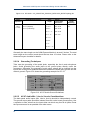
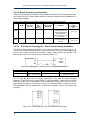
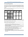
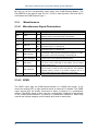
Table 2-38 TV DAC Video filter components
Component
C1
C2
Value
6 pF
6 pF
150 Ω@
100 MHz
FB
Tolerance
Voltage/Current
± 20%
± 20%
16 V
16 V
± 25%
100 mA
Type
Ceramic
Ceramic
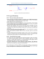
2.11.3 Layout Guidelines
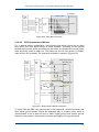
2.11.3.1 TV DAC routing
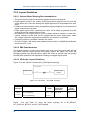
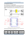
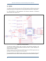
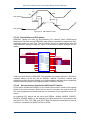
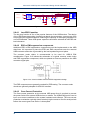
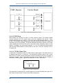
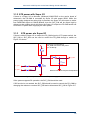
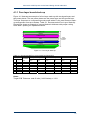
The minimum spacing between each TV DAC signal is 40 mils, but 50 mils is
preferred. A maximum amount of spacing should be used between each TV DAC
signal as well as to all other toggling signals. This helps prevent crosstalk between
the TV DAC signals and other signals. The routing for each TV DAC signal should
also be matched and balanced. All TV DAC signals should be routed on the same
layer, have a similar number of bends, the same number of vias, etc. All routing
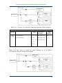
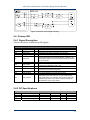
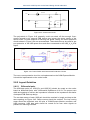
should be done with ground referencing as well. Figure 5-37 shows the TV DAC
routing topology. Total length of each signal should be less than 12 inches. Intra-pair
length difference should be less than 200 mils.
Carrier board
COM-Express
Spacing
>50 mils
TV_ DAC _A
Zo=50O
Spacing
>40 mils
150ohm
Chipset
TV_DAC _B
Spacing
>40 mils
TV_ DAC _C
150ohm
MAX =0.2"
Zo=50O
Spacing
>50 mils
150ohm
150 ohm
MAX =0.2"
Zo=50O
150ohm
3.3V
MAX =0.2"
150ohm
Video
Filter
MAX=0.5‘
Zo=75 ohm
Video
Filter
Connector
MAX=0.5‘
Zo=75 ohm
Video
Filter
3.3V
75 ohm Coaxial Cable
3.3V
MAX=0.5‘
Zo=75 ohm
Figure 2-51 TV DAC Schematic
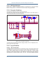
2.12 LPC
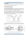
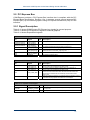
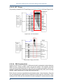
COM-Express provides a LPC interface to some devices as Super I/O, FWH, TPM,
and others.
2.12.1 Signal Description
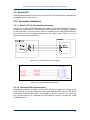
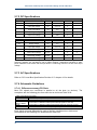
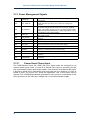
Table 2-39 shows COM-Express LPC signals.
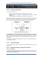
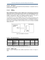
Table 2-39 LPC signals description
Pin
B4,5,6,7
Signal
LPC_AD[0:3]
I/O
O
Description
LPC multiplexed address, command and data bus
57
TV