1
Design Guide
COM-Express
Carrier Board Design Guide
Advantech COM-Express Carrier Board Design Guide Addendum
Notices
The copyright on this user manual remains with Advantech Co., Ltd. No part of this user
manual may be transmitted, reproduced, or changed.
Other companies’ product names that may be used herein remain the property of their
respective owners.
The product specifications, design and this user’s manuals content are subject to change
without notice.
If you have any questions, please contact your merchant or our service center for
clarification. We are not responsible for any losses resulting from using this product no
matter what the reason.
Revision History
Version/Revision date
Version 1.0
Version 1.1
Version 1.2
Version 2.0
Version 2.1
Part No. 2006001801
Printed in Taiwan
2
Date
July, 2006
July, 2007
April, 2009
May, 2010
August, 2010
Description
Initial release
Change format to Addendum
Edition 2.1
August 2010
Notices
Advantech COM-Express Carrier Board Design Guide Addendum
Table of Contents
Table of Contents .......................................................................................................3 Chapter 1 Introduction............................................................................................7 1.1 COM-Express Overview ................................................................ 7 1.2 Terminology .................................................................................. 8 Table 1.1 Conventions and Terminology .......................................8 1.3 Referenced Documents .............................................................. 10 Table 1.2 Referenced Documents ...............................................10 Chapter 2 Carrier Board Schematic Guidelines .................................................11 2.1 Gigabit Ethernet (GBE) ............................................................... 11 2.1.1 Signal Descriptions .......................................................................11 2.1.2 DC Specifications .........................................................................11 2.1.3 Schematic Guidelines ...................................................................12 2.1.4 Layout Guidelines .........................................................................13 2.2 AC’97 Audio / HD Audio .............................................................. 18 2.2.1 Signal Description .........................................................................18 2.2.2 DC Specifications .........................................................................18 2.2.3 AC’97 Audio Spec.........................................................................18 2.2.4 Schematic Guidelines ...................................................................19 2.2.5 Layout Guidelines .........................................................................22 2.3 Serial ATA ................................................................................... 25 2.3.1 Schematic Guidelines ...................................................................25 2.3.2 Layout Guidelines .........................................................................26 2.4 Primary IDE ................................................................................. 27 2.4.1 Signal Description .........................................................................27 2.4.2 DC Specifications .........................................................................27 2.4.3 IDE Spec.......................................................................................28 2.4.4 Schematic Guidelines ...................................................................28 2.4.5 Layout Guidelines .........................................................................30 2.5 PCI Express Bus ......................................................................... 31 2.5.1 Signal Description .........................................................................31 2.5.2 Schematic Guidelines ...................................................................32 2.5.3 Layout Guidelines .........................................................................35 2.6 SDVO .......................................................................................... 38 2.7 PCI-Bus ....................................................................................... 39 2.7.1 Signal Description .........................................................................39 2.7.2 DC Specifications .........................................................................40 2.7.3 AC Specifications..........................................................................40 2.7.4 Schematic Guidelines ...................................................................40 2.7.5 Layout Guidelines .........................................................................44 2.8 Universal Serial Bus (USB) ......................................................... 47 2.8.1 Signal Description .........................................................................47 2.8.2 DC Specifications .........................................................................47 2.8.3 USB Spec. ....................................................................................47 2.8.4 Schematic Guidelines ...................................................................47 2.8.5 Layout Guideline ...........................................................................49 2.9 LVDS ........................................................................................... 51 2.9.1 Signal Description .........................................................................51 2.9.2 DC Specifications .........................................................................51 2.9.3 Schematic Guidelines ...................................................................51 2.9.4 Layout Requirements....................................................................52 Table of Contents
3
Advantech COM-Express Carrier Board Design Guide Addendum
2.10 VGA ............................................................................................ 53 2.10.1 Signal Description .........................................................................53 2.10.2 DC Specifications .........................................................................53 2.10.3 VGA Specifications .......................................................................54 2.10.4 Schematic Guidelines ...................................................................54 2.10.5 Layout Guideline ...........................................................................54 2.11 TV-Out ........................................................................................ 55 2.11.1 Signal Description .........................................................................55 2.11.2 Schematic Guidelines ...................................................................55 2.11.3 Layout Guidelines .........................................................................57 2.12 LPC ............................................................................................. 57 2.12.1 Signal Description .........................................................................57 2.12.2 Schematic Guidelines ...................................................................58 2.12.3 Layout Guidelines .........................................................................58 2.12.4 Application Notes for Super I/O Functions....................................58 2.13 Power Management Signals ....................................................... 62 2.13.1 Power Good / Reset Input ............................................................62 2.13.2 Reset signals ................................................................................63 2.14 Miscellaneous ............................................................................. 64 2.14.1 Miscellaneous Signal Descriptions ...............................................64 2.14.2 SPKR ..........................................................................................64 2.14.3 I2C Bus .........................................................................................65 2.14.4 I2C Spec .......................................................................................66 2.14.5 SMBus ..........................................................................................66 2.14.6 WDT ..........................................................................................67 Chapter 3 Power Management and Power Delivery...........................................68 3.1 Power Design Guidelines ............................................................ 68 3.1.1 ATX Power Delivery Block Diagram .............................................68 3.1.2 ATX power with Super I/O ............................................................69 3.1.3 ATX power w/o Super I/O .............................................................69 3.1.4 AT Power Delivery Block Diagram................................................70 3.1.5 AT Power Working as ATX Mode .................................................71 Chapter 4 PCB Layout Guidelines .......................................................................72 4.1 Nominal Board Stack-Up ............................................................. 72 4.1.1 Four-layer board stack-up.............................................................73 Table 4-1 Recommended Four-Layer Stack-Up Dimensions ......73 4.1.2 Six-layer board stack-up ...............................................................74 4.2 Alternate Stack Ups .................................................................... 75 4.3 Differential Impedance Targets for Trace Routing....................... 75 Chapter 5 Mechanical Schematic Guidelines .....................................................76 5.1 COM-Express Mechanical Dimensions ....................................... 76 5.2 COM Express Module Connector................................................ 77 5.3 COM Express Carrier Board Connector ...................................... 77 5.4 COM Express Connector PCB Pattern ....................................... 78 4
Table of Contents
Advantech COM-Express Carrier Board Design Guide Addendum
Figure 2-1 10/100M Ethernet Connections ..............................................................12 Figure 2-2 Gigabit Ethernet Connections .................................................................12 Figure 2-3 Gigabit Ethernet Connections with Integrated Magnetic ..........................13 Figure 2-4 Differential signals route example...........................................................14 Figure 2-5 Bend layout example ..............................................................................15 Figure 2-6 10/100M Ethernet Interconnection...........................................................15 Figure 2-7 Gigabit Ethernet Interconnection .............................................................16 Figure 2-8 Critical Dimensions ...................................................................................17 Figure 2-9 AC’97 Audio Connections ........................................................................19 Figure 2-10 HD Audio Connections ..........................................................................20 Figure 2-11 Jack Detection with sensing resistors ....................................................20 Figure 2-12 Reference Audio Schematic .................................................................21 Figure 2-13 HD Audio – AC_SDIN Topology ............................................................22 Figure 2-14 HD Audio – AC_SDOUT/AC_SYNC/AC_BITCLK/AC_RST# Topology
#1 ...............................................................................................................................23 Figure 2-15 HD Audio – AC_SDOUT/AC_SYNC/AC_BITCLK/AC_RST# Topology
#2 ...............................................................................................................................24 Figure 2-16 AC’97 Audio Ground Guidelines ............................................................24 Figure 2-17 SATA interconnection example ............................................................25 Figure 2-18 SATA Schematic Reference ..................................................................25 Figure 2-19 SATA LED Schematic Reference ..........................................................26 Figure 2-20 SATA traces length matching .................................................................27 Figure 2-21 IDE Master/Slave Handshake Signals Connection...............................28 Figure 2-22 IDE Master/Slave DASP-S# Signals Connection .................................28 Figure 2-23 IDE Bus Trace Length on Carrier Board ................................................29 Figure 2-24 IDE Connections ....................................................................................29 Figure 2-25 CF Connections .....................................................................................30 Figure 2-26 PCI Express Interconnect Example .......................................................32 Figure 2-27 PCI Express Connector Schematic Reference ......................................32 Figure 2-28 Polarity Inversion on a TX to RX Interconnect .......................................33 Figure 2-29 Lane Reversal and Polarity Inversion - TX to RX Interconnect .............34 Figure 2-30 Trace Length Matching in Each Segment..............................................35 Figure 2-31 Topology #1 – COM Express to PCI Express Device Down .................36 Figure 2-32 “interleaved” (left) and “non-interleaved” pairs (right) ............................36 Figure 2-33 Topology #2 and #3 – COM Express to Express Card or Docking
Connector...................................................................................................................37 Figure 2-34 CH7308 Schematic ................................................................................38 Figure 2-35 Interrupt Routing of PCI Slots / Devices on carrier board ......................41 Figure 2-36 Interrupt Routing and IDSEL Schematic Reference ..............................42 Figure 2-37 Clock Skew of PCI .................................................................................43 Figure 2-38 Design Example: PCI Arbiter .................................................................43 Figure 2-39 PCI Bus Layout Example with IDSEL ....................................................45 Figure 2-40 PCI Clock Layout Example .....................................................................46 Figure 2-41 USB Connections ..................................................................................48 Figure 2-42 Common Mode Choke and ESD suppression design ...........................48 Figure 2-43 Overcurrent Circuit.................................................................................49 Figure 2-44 Power Switch with Overcurrent Protection Circuits ...............................49 Figure 2-45 USB Layout Guidelines..........................................................................50 Figure 2-46 Violation of Proper Routing Techniques ................................................50 Figure 2-47 One LVDS Differential Pair with Choke Design .....................................51 Figure 2-48 VGA reference schematic ......................................................................54 Figure 2-49 Connection Diagram of TV-out ..............................................................56 Figure 2-50 TV DAC Video Filter ..............................................................................56 Figure 2-51 TV DAC Schematic ................................................................................57 Chapter 1 Introduction
5
Advantech COM-Express Carrier Board Design Guide Addendum
Figure 2-52 Architecture of LPC interface .................................................................58 Figure 2-53 Serial Bus Connection ...........................................................................59 Figure 2-54 Keyboard and Mouse connection ..........................................................59 Figure 2-55 LPT Connection .....................................................................................60 Figure 2-56 Floppy Connection .................................................................................60 Figure 2-57 Power Good / Reset Input Applications .................................................63 Figure 2-58 Speaker Schematics ..............................................................................65 Figure 2-59 I2C Bus Connections .............................................................................65 Figure 2-60 SMB Bus Connections ...........................................................................66 Figure 3-1 ATX Power Delivery Block Diagram ........................................................68 Figure 3-2 power circuits for ATX power supply w/o SIO ..........................................69 Figure 3-3 AT Power Delivery Block Diagram...........................................................70 Figure 3-4 ATX Working Model Based on AT Power Input Reference Schematics ..71 Figure 4-1 Four-Layer Stack-up ................................................................................73 Figure 4-2 Six-Layer Stack-up ..................................................................................74 Figure 5-1 COM-Express Module Board Mechanical Dimensions ............................76 Figure 5-2 COM-Express Module Receptacle ..........................................................77 Figure 5-3 COM-Express Carrier Board Plug (8mm Version) ...................................78 Figure 5-4 COM-Express Connector PCB Pattern....................................................78 6
Chapter 1 Introduction
Advantech COM-Express Carrier Board Design Guide Addendum
Chapter 1
Introduction
This design guide addendum organizes and provides Advantech’s COM carrier board
design recommendations for COM-Express Modules. All other Schematic Guidelines
for the carrier board are applicable and can be found in the PICMG Design Guide
V1.0.
Please contact Advantech sales/application engineer if there are any questions about
designing the carrier board, or you plan to use this processor in applications other
than mobile or desktop platforms.
1.1 COM-Express Overview
COM-Express complies with COM Express standard from the PCI Industrial
Computer Manufacturers Group (PICMG) which provides next generation
performance of the smallest state of the art embedded modules. Advantech’s COM
Design Support Services (CDSS) help customers develop and integrate their carrier
board with Advantech’s COM modules. CDSS provides a series of valuable services
such as Product, Design Assistance, Software and Thermal Solution services,
together they help reduce design risks when designing carrier boards. For more
details, please visit “http://com.advantech.com”
Advantech offers a wide range of COM products to cater to each customer's
demands. The modular designs add more flexibility to the system. The COM Express
form factor allows the COM-Express Modules to be easily and securely mounted on
a customized solution board. The design and multiple processor choices eliminate
CPU integration worries and allow fast application support for the most dynamic
embedded needs.
COMs are widely used modular CPU boards with high integration features. COMExpress supports a wide range of processor and chipsets. They include technologies
like: PCI Express, Serial ATA, USB 2.0, etc. Not only do COMs allow quick design,
they also provide the benefits of easy installation, maintenance and upgrade ease.
7
Advantech COM-Express Carrier Board Design Guide Addendum
Though small in size, COMs implement CPU architectures and basic common
circuits. Many system integrators find that Advantech COM solutions already cover
around 80% of their feature requirements. This makes COM products powerful time
and cost savers.
1.2 Terminology
Table 1.1 Conventions and Terminology
AC’97
Codec 97’ Audio interface
A serial port interface on IBM PC-compatible computers running
COM
Microsoft Windows or MS-DOS
COM-Express
New generation technology of Computer On Module
CPU
Central processing Unit
CRT
Cathode Ray Tube
DDR2
Double Data Rate second generation SDRAM memory technology
DVI
Digital Visual Interface
DVO
Digital Video Out
EMI
Electromagnetic Interference
ESD
Electrostatic Discharge
A hardware standard replacing PC cards supported both PCI Express
ExpressCard
and USB 2.0 connectivity
FSB
Front Side Bus, synonymous with Host or CPU bus
GMCH
Refers to the Graphics Memory Controller Hub chipset component
HD Audio
High Definition Audio
8
Advantech COM-Express Carrier Board Design Guide Addendum
I2C
IDE (ATA)
INTx
LAN
LCD
LPC
LVDS LCD
MCH
NTSC
PAL
PCI
PCI-Express
RTC
SATA
SDVO
SMBus
TMDS
TV
UART
USB
Inter-IC (a two wire serial bus created by Philips)
Integrated Drive Electronics (Advanced Technology Attachment)
An interrupt request signal where x stands for interrupts A, B, C, and
D.
A local area network (LAN) is a computer network covering a small
physical area
Liquid Crystal Display
The Low Pin Count (LPC) Interface Specification for legacy I/O has
facilitated the industry's transition toward ISA-less systems.
Low Voltage Differential Signaling: A high speed, low power data
transmission standard used for display connections to LCD panels.
Refers to the Memory Controller Hub chipset component
National Television Standards Committee
Phase Alternate Line
Peripheral Component Interface
New generation PCI interface with serial interconnection technology
Real Time Clock
Serial ATA interface
Serial Digital Video Out
System Management Bus.
Transition Minimized Differential Signaling
Television supports NTSC and PAL
A universal asynchronous receiver/transmitter that translates data
between parallel and serial forms.
Universal Serial Bus
9
Advantech COM-Express Carrier Board Design Guide Addendum
1.3 Referenced Documents
Table 1.2 Referenced Documents
Document
Location
ACPI - Advanced
Configuration and Power
http://www.acpi.info/
Management Specification
http://download.intel.com/support/motherboards/desktop/sb/ac97_r23
AC’97 AUDIO
.pdf
APM - Advanced Power
http://www.microsoft.com/whdc/archive/amp_12.mspx
Management Specification
COM Express Specification http://www.picmg.org/
Ethernet(IEEE 802.3)
http://standards.ieee.org/getieee802/802.3.html
I2C Bus Interface
http://www.semiconductors.philips.com/buses/i2c
PCI
http://www.pcisig.com/
RS232
http://www.eia.org/
SMBus
http://www.smbus.org/specs/
USB
http://www.usb.org/home
10
Advantech COM-Express Carrier Board Design Guide Addendum
Chapter 2
Carrier Board Schematic Guidelines
2.1 Gigabit Ethernet (GBE)
COM-Express supports the IEEE802.3 network interface and flexible dynamically
loadable EEPROM algorithm. The network interface complies with the IEEE standard
for 10BASE-T, 100BASE-T and 1000BASE-T Ethernet interfaces.
2.1.1 Signal Descriptions
Table 2-1 shows COM-Express Ethernet signals, including pin number, signal
naming, I/O, and descriptions.
Table 2-1 GBE signals
Pin
Signal
I/O
Description
A13,A9,A7,A3
A12,A10,A6,A2
GBE0_MDI[0:3]+
GBE0_MDI[0:3]-
I/O
Gigabit Ethernet Controller 0: Media Dependent Interface
Differential Pairs 0,1,2,3. The MDI can operate in 1000,
100 and 10 Mbit / sec modes. Some pairs are unused in
some mode, per the following:
1000BASE-T
100BASE-TX
10BASE-T
B1_DA+/B1_DB+/B1_DC+/B1_DD+/-
TX+/RX+/-
TX+/RX+/-
MDI[0]+/MDI[1]+/MDI[2]+/MDI[3]+/B2
A8
A4
GBE0_ACT#
GBE0_LINK#
GBE0_LINK100#
OD
OD
OD
A5
GBE0_LINK1000#
OD
A14
GBE0_CTREF
REF
Gigabit Ethernet Controller 0 activity indicator, active low.
Gigabit Ethernet Controller 0 link indicator, active low.
Gigabit Ethernet Controller 0 100 Mbit / sec link indictor,
active low.
Gigabit Ethernet Controller 0 1000 Mbit / sec link indictor,
active low.
Reference voltage for Carrier board Ethernet channel 0
magnetics center tap. The reference voltage is determined
by the requirements of the module PHY and may be as
low as 0 V and as high as 3.3 V.
The reference voltage output shall be current limited on
the module. In the case in which the reference is shorted
to ground, the current shall be limited to 250 mA or less.
2.1.2 DC Specifications
Table 2-2 GBE I/O Voltage
Symbol
VIL
VIH
VOL
VOH
Parameter
Input Low Voltage
Input High Voltage
Output Low Voltage
Output High Voltage
Min
-1.7
0
2.1
Max
0.9
-0.5
3.6
Unit
V
V
V
V
Note
*1
Note *1. Vcc is 3.3V ( from 3.0V min. to 3.6V max.)
11
Advantech COM-Express Carrier Board Design Guide Addendum
2.1.3 Schematic Guidelines
2.1.3.1
Differential Pairs
Designing for Gigabit Ethernet operation is very similar to the designing for 10/100
Mbps. 10/100Mbps Ethernet has two differential pairs, and Gigabit Ethernet has four
differential pairs. Figure 2-1 and Figure 2-2 show the 10/100M Ethernet and Gigabit
Ethernet Connections.
Figure 2-1 10/100M Ethernet Connections
LAN Connector
COMExpress
GBE0_MDI[0]+
GBE0_MDI[0]GBE0_MDI[1]+
GBE0_MDI[1]GBE0_MDI[2]+
GBE0_MDI[2]GBE0_MDI[3]+
GBE0_MDI[3]-
Magnetic
Module
(Transformer)
RJ45
GBE0_ACT#
GBE0_LINK#
GBE0_LINK100#
GBE0_LINK1000#
Figure 2-2 Gigabit Ethernet Connections
2.1.3.2
Center Tap connection of Transformer
The COM-E signal GBE0_CTREF pin A14 should be connected directly to the center
tap of the transformer. The center tap voltage is the output from the COM-Express
12
Advantech COM-Express Carrier Board Design Guide Addendum
Module to the carrier board usually 1.8V, 2.5V, or another voltage, depending on the
LAN chip design.
2.1.3.3
LAN Connector with Integrated Magnetic
For simplifying the schematic and layout considerations of LAN connector, it is
strongly recommended to use the RJ45 LAN connector. Figure 2-3 shows the
integrated magnetic schematic.
3
R321
LAN_ACT#
0
VCC3.3V
3
11
R52
R54
GBE0_CTREF
220
0
12
CN3A
RJ45+USB*2
Y
1
LAN_MDI0P_R
2
LAN_MDI0N_R
3
LAN_MDI1P_R
4
LAN_MDI1N_R
5
LAN_MDI2P_R
6
LAN_MDI2N_R
7
LAN_MDI3P_R
8
LAN_MDI3N_R
9
1
75
0.1uF
2
3
75
0.1uF
6
4
75
0.1uF
5
7
R64
3
O
13
LAN_LINK100#
LAN_LINK1000#
0.1uF
R323
0
LINK1000#
R140
220
8
10
14
G
1000pF
2kV
SHIELD GND
23
24
25
26
3
TCT22
0
75
GND_F
Figure 2-3 Gigabit Ethernet Connections with Integrated Magnetic
2.1.3.4
Implementation of Ethernet LED indicators
RJ-45 connector with LED indicators needs 3.3V to drive the LEDs. The Link and
activity LEDs can be implemented by using the COM-Express Module’s GBE0_ACT#,
GBE0_LINK#, GBE0_LINK100#, and GBE0_LINK1000# pins. The sink current is
connected to the cathode of the LED, and the anode of the LED should be pulled to
3.3V through a resistor as 220 Ω.
2.1.4 Layout Guidelines
Route the transmit and receive lines on the carrier board as differential pairs, with a
differential impedance of 100 Ω. PCB layout software allows determination of the
proper trace width and spacing to achieve the impedance after the PCB stack-up
configuration.
The TX+/TX- signal pair should be well separated from the RX+/RX- signal pair. Both
pairs should be well separated from any other signals on the PCB. The total routing
length of these pairs from the COM-Express Module to the Ethernet RJ45 connector
should be made as short as practical.
For Ethernet connector placement, place it as close as possible to the COM-Express
Module pins to shorten the routing lengths of all Ethernet signals. Differential signal
traces should be kept as short as possible to decrease the possibility of being
13
Advantech COM-Express Carrier Board Design Guide Addendum
affected by high frequency noise from other signals and power planes, and capacitive
loading is also reduced.
Please refer to the Advantech layout checklist for detail.
2.1.4.1
z
z
z
z
z
z
Differential pairs design considerations
Maintain constant symmetry and spacing between the traces within a differential
pair. Keep the signal trace lengths of a differential pair equal to each other. Do
not use serpentines to try to match trace lengths in the differential pair.
Serpentines cause impedance variations causing signal reflections, which can be
a source of signal distortion. Try to keep the length difference of the differential
pair less than 5 mil.
The total length of each differential pair should be less than 4 inches. Keep the
length of each differential pair under 4 inches. Figure 2-4 shows an example.
Please refer to the Advantech layout checklist for detailed length matching.
Do not route the transmit differential traces closer than 50 mils to the receive
differential traces for 10/100 Mbps.
Do not route any other signal traces (including other differential pairs) parallel to
the differential traces or closer than 50 mils. to the differential traces. Figure 2-4
shows an example. It’s recommended to keep length L3 longer than 50 mils.
Keep separate traces within a differential pair as small as possible down to 5 to 8
Mils, depending on the impedance control. Close separation of the traces allow
the traces to couple well to each other.
For high-speed signals, they should minimize the number of corners and vias. If a
90° bend is required, it is recommended to use two 45° bends instead. Figure 2-5
shows the example.
COM-Express
Carrier board
Differential
Pairs
L1
L2
On board
LAN chip
L3
Transformer
+ RJ45
Differential
Pairs
Figure 2-4 Differential signals route example
14
Advantech COM-Express Carrier Board Design Guide Addendum
Figure 2-5 Bend layout example
2.1.4.2
Transformer
It’s recommended to use the integrated Magnetic Modules/RJ-45 LAN connectors. If
using the discrete Magnetic Modules and RJ-45 connector, the transformer should be
placed close to the RJ-45 LAN connector to reduce EMI emissions. Each differential
pair of data signals is required to be parallel to each other with the same trace length
on the component (top) layer and to be parallel to a respective ground plane.The
connector with integrated magnetic is much simplified for layout. The more complex
layout as Figure 2-6 and Figure 2-7 shows the 10/100M and Gigabit Ethernet layout
with discrete magnetic.
Figure 2-6 10/100M Ethernet Interconnection
15
Advantech COM-Express Carrier Board Design Guide Addendum
Figure 2-7 Gigabit Ethernet Interconnection
2.1.4.3 Power Considerations
In general, any section of traces that are intended for use with high-speed signals
should observe proper termination practices. Many board layouts remove the ground
plane underneath the transformer and the RJ-45 connector to minimize capacitive
coupling of noise between the plane and the external Ethernet cable.
2.1.4.4 Critical Dimensions
There are two critical dimensions that must be considered during the layout phase of
an Ethernet controller. These dimensions are identified in Figure 2-8 as distance A
and B.
Distance A: Transformer to RJ-45 LAN Connector (Priority 1). The distance labeled A
should be given the highest priority in the backplane layout. The distance between
the transformer module and the RJ-45 connector should be kept to less than 1 inch
of separation. The following trace characteristics are important and should be
observed:
1. Differential Impedance: The differential impedance should be 100 Ω. The
single ended trace impedance will be approximately 50 Ω; however, the
differential impedance can also be affected by the spacing between the
traces.
2. Trace Symmetry: Differential pairs should be routed with consistent
separation and with exactly the same lengths and physical dimensions (for
example, width and spacing).
Distance B: From COM-Express Module to Transformer (Priority 2). Distance B
should also be designed to be as short as possible. Be sure not to route Distance B
16
Advantech COM-Express Carrier Board Design Guide Addendum
over 2.5 inches for Intel’s layout guide. The high-speed signals propagating through
these traces require the shortest distances between these components.
COMExpress
GBE_MDI[0]+
GBE_MDI[0]-
.
.
.
LAN Connector
Magnetic
Module
(Transformer)
RJ45
GBE_MDI[3]+
GBE_MDI[3]-
B :2.5 inches max
A:1 inches max
Figure 2-8 Critical Dimensions
17
Advantech COM-Express Carrier Board Design Guide Addendum
2.2 AC’97 Audio / HD Audio
COM-Express provides an AC’97 Audio / HD Audio interface which is compliant to
AC’97 AUDIO Rev. 2.3 Specification and the HD Audio Specification. Please
establish the CODEC of AC’97 Audio / HD Audio on the carrier board for your
application.
2.2.1 Signal Description
Table 2-3 shows COM-Express AC’97 Audio / HD Audio interface signals, including
pin number, signals, I/0 and descriptions.
Table 2-3 Audio signals description
Pin
Signal
I/O
A30
AC_RST#
O
A29
AC_SYNC
O
A32
AC_BITCLK
I/O
A33
B30,B29,
B28
AC_SDOUT
O
AC_SDIN[0:2]
I
Description
AC’97 Audio / HD Audio : Reset output to AC97 CODEC, active
low
AC’97 Audio / HD Audio : 48 kHz fixed-rate, samplesynchronization signal to the CODEC(s)
AC’97 Audio: Bit Clock Input: This signal is a 12.288 MHz serial
data clock generated by the external codec(s). This signal has an
integrated pull-down resistor
HD Audio: Bit Clock Output: This signal is a 24 MHz serial data
clock generated by COM-Express. This signal has an integrated
pull-down resistor so that AC_BITCLK does not float when an HD
Audio codec (or no codec) is connected but the signals are
temporarily configured as AC’97 AUDIO.
AC’97 Audio / HD Audio : Serial TDM data output to the CODEC
AC’97 Audio / HD Audio : Serial TDM data inputs from up to 3
CODECs
2.2.2 DC Specifications
Table 2-4 AC’97 AUDIO CODEC DC specification
Symbol
Dvdd
Avdd
Vil
Vih
Parameter
Digital supply voltage
Analog supply voltage
Input Low Voltage
Input High Voltage
Min
Dvdd+5%
4.75
0.65Vdd
Max
Dvdd+5%
5.25
0.35Vdd
-
Unit
V
V
V
V
Note
*1. Dvdd=5V or 3.3V
Table 2-5 AC’97 AUDIO CODEC analog I/O DC specification
Symbol
AUXAL/R
MIC
SNDL/R
Parameter
Full scale input voltage
Full scale input voltage
Full scale output voltage
Min
-
Typ
1.0
0.1
1.0
Max
-
Unit
Vrms
Vrms
Vrms
Note
2.2.3 AC’97 Audio Spec
Refer to “Audio Codec ’97 Revision 2.1 May 22, 1998” Chapter 9 for digital signals
AC spec. and Chapter 10 for analog performance spec.
18
Advantech COM-Express Carrier Board Design Guide Addendum
2.2.4 Schematic Guidelines
AC97 and HD Audio are the popular architectures for implementing audio, modem,
and communications functionality in the IPC market. The architecture of the COMExpress HD Audio allows a maximum of three CODECs to be connected.
2.2.4.1 Connection of AC’97 Audio and HD Audio
2.2.4.2 AC’97 Audio:
The Figure 2-9 shows the connections for COM-Express AC’97 Audio signals with
three Codecs.
AC/MC/AMC
COM-Express
AC_RST#
AC_SDOUT
AC_SYNC
AC_BITCLK
AC_SDIN[0]
AC_SDIN[1]
AC_SDIN[2]
Primary
Codec
AC/MC/AMC
Secondary
Codec
AC/MC/AMC
Tertiary
Codec
Figure 2-9 AC’97 Audio Connections
The clock is provided from the primary codec on the link via AC_BITCLK, and it is
derived from a 24.576 MHz crystal or oscillator. Refer to the primary codec vendor for
crystal or oscillator requirement. AC_BITCLK is a 12.288 MHz clock driven by the
primary codec to the COM-Express digital controller on board and to the other
codec(s) on the carrier board.
2.2.4.3 HD Audio:
Figure 2-10 shows the connections for COM-Express HD Audio signals with three
HD Codecs. The clock of is provided from the COM-Express module via AC_BITCLK
signal. The AC_BITCLK is a 24 MHz clock driven by the COM-Express module as an
output to the codec present on the carrier board.
19
Advantech COM-Express Carrier Board Design Guide Addendum
AC/MC/AMC
COM-Express
AC_RST#
AC_SDOUT
AC_SYNC
AC_BITCLK
AC_SDIN[0]
AC_SDIN[1]
AC_SDIN[2]
Primary
Codec
AC/MC/AMC
Secondary
Codec
AC/MC/AMC
Tertiary
Codec
Figure 2-10 HD Audio Connections
Note: AC’97 Audio and HD Audio are mutually exclusive and cannot be used at the
same time on a platform.
2.2.4.4
HDA Audio Jack Detection Function
The HDA audio jack connectors should be designed to detect and inform the
operating system which jack is plugged or un-plugged. It can be done by the sensing
resistors and the programmable GPIO pins. Figure 2-11 shows the example of jack
detection function with sensing resistors. Please refer to the codec specification to
get more information.
Figure 2-11 Jack Detection with sensing resistors
The schematic of the evaluation board is shown in Figure 2-12.
20
Advantech COM-Express Carrier Board Design Guide Addendum
R108
10K
MIC1-VREFO-R
0
R110
+5VA
LINE2-VREFO
C357 0.1u
MIC2-VREFO
C358 0.1u
LINE1-VREFO-L
MIC1-VREFO
+5VA
FRONT-L
C105
R121
0
45
SIDESURR-R
R122
0
46
10K
R123
47
25
AVDD1
27
VREF
29
28
MIC1-VREFO-L
30
MIC2-VREFO
LINE1-VREFO-L
32
33
34
31
LINE2-VREFO
MIC1-VREFO-R
DCVOL
CD-L
LFE
MIC2-R
SIDESURR-L
MIC2-L
SIDESURR-R
LINE2-R
SPDIFI/EAPD
LINE2-L
SPDIFO
GPIO0
2
1
DVDD1
48
CEN
Sense A
SYNC
SIDESURR-L
CD-GND
10
44
ALC888
AVSS2
DVDD2
LFE
CD-R
9
43
SURR-R
SDATA-IN
CEN
MIC1-L
DVSS2
42
LINE1-L
JDREF/NC
8
41
LINE1-R
MIC1-R
BIT-CLK
0
10u/12
U5
SURR-L
7
R118
40
SDATA-OUT
SURR-R
R116
6
20K
5
39
0
AVDD2
DVSS1
R117
LINE1-VREFO-R
GPIO1
38
4
37
3
LINE1-VREFO-R
10u/12
Sense B
C107
SURR-L
35
FRONT-R
+5VA
C106
10u/12
FRONT-L
36
FRONT-R
24
LINE1-R
23
LINE1-L
22
MIC1-R
21
MIC1-L
20
CD-R
19
CD-GND
18
CD-L
17
MIC2-R
16
MIC2-L
15
LINE2-R
MIC2-R
C362 0.1u
29
To mini-PCI
LINE2-R
29
LINE2-L C359 0.1u
14
13 R124
C361 0.1u
0
SenseA
PCBEEP
R113
MIC1-VREFO-L
0
12
10K
R105
SenseB
0
26
CEN-JD
R112
AVSS1
R111
RESET#
5.1K
11
SIDESURR-JD
5.1K
R127
FRONT-JD
10K
R125
LINE1-JD
20K
R128
MIC1-JD
39.2K
R129
SURR-JD
VCC3.3V
VDD3.3
L26
11P600S
C124
C203
0.1u
R130
22
10u/12
R131
22
AC97_RST#
3,29
AC97_SY NC
3,29
AC97_SDIN0
3,29
AC97_BITCLK
3,29
C125
22P
AC97_SDOUT 3,29
MIC1-VREFO-R
CENTER/LFE
AUDIO
CN12E
MIC1-VREFO-L
R106
4.7K
MIC1-R
MIC1-L
C97
1u
C99
1u
R107
4.7K
FRONT_OUT
AUDIO
CN12C
MIC1-R1
L14
11B102S
MIC1-R2
MIC1-L1
L16
11B102S
MIC1-JD
MIC1-L2
C101
100p
SURR-R
SURR-L
C98
C100
1u
1u
SURR-R1
L15
11B102S
SURR-R2
SURR-L1
L17
11B102S
SURR-JD R109
SURR-L2
C02
C4
C3
C2
C1
C103
100p
0
C01
E4
E3
E2
E1
C104
100p
C102
100p
GND_F
C108 100uF/6.3V/TC-B
FRONT-R1
1
2
FRONT-L
C110 100uF/6.3V/TC-B
FRONT-L1
1
2
+
+
FRONT-R
L18
L20
11B102S
FRONT-R2
11B102S
FRONT-JD
FRONT-L2
C112
100p
SURROUND
AUDIO
CN12D
MIC1_IN
AUDIO
CN12B
GND_F
LFE
C02
B4
B3
B2
B1
CEN
C109
1u
C111
1u
LFE1
L19
11B102S
LFE2
CEN1
L21
11B102S
CEN-JD
CEN2
C114
100p
C113
100p
C01
D4
D3
D2
D1
C115
100p
LINE1-VREFO-R
LINE1-VREFO-L
R119
4.7K
R120
4.7K
GND_F
GND_F
LINE1_IN
AUDIO
CN12A
LINE1-R
LINE1-L
C116
1u
C118
1u
LINE1-R1
LINE1-L1
L22
L24
11B102S
LINE1-R2
11B102S
LINE1-JD
LINE1-L2
C120
100p
C02
A4
A3
A2
A1
SIDESURR
AUDIO
CN12F
C117
SIDESURR-R
1u
C119
1u
SIDESURR-L
SIDESURR-R1 L23
11B102S
SIDESURR-L1 L25
SIDESURR-JD
R126
SIDESURR-L2
11B102S
C121
100p
SIDESURR-R2
C122
100p
0
C01
F4
F3
F2
F1
C123
100p
GND_F
GND_F
Figure 2-12 Reference Audio Schematic
21
Advantech COM-Express Carrier Board Design Guide Addendum
2.2.5 Layout Guidelines
2.2.5.1 General Board Routing Recommendations
z
z
z
z
z
z
z
The ground return paths for the analog signals should be considered.
Digital signals routed in the vicinity of the analog audio signals must not cross the
power plane split. Place the analog and digital signals as far as possible from each
other.
Partition the board with all analog components grouped together in one area and all
digital components in another.
Keep digital signal traces, especially the clock, as far away as possible from the
analog inputs and voltage reference pins.
All resistors in the signal path or on the voltage reference should be metal film.
Carbon resistors can be used for DC voltages and the power supply path, where
the voltage coefficient, temperature coefficient, and noise are not factors.
Locate the crystal or oscillation closed to the codec.
The AC’97 Audio / HD Audio trace impedance from codec to COM-Express Module
should be 55 Ω ± 15%.
2.2.5.2 EMI Considerations
The signals entering or leaving the analog area must cross the ground split through
the beads between digital ground and analog ground. No signal can cross the
split/gap between the ground planes, which will cause a ground loop and greatly
increase EMI emissions and degrade the analog and digital signal quality.
2.2.5.3 HD Audio Layout Guidelines
Figure 2-13 and Table 2-6 show the AC_SDIN layout topology.
Carrier board
COM-Express
L1
L2
Audio Codec
(down)
R1
Figure 2-13 HD Audio – AC_SDIN Topology
Table 2-6 HD Audio – AC_SDIN Routing
Trace
Impedance
55 Ω
+/- 15%
HD Audio Requirements
Trace
length
5 on 7 (stripline)
L1= 1“ – 11“
5 on 7 (microstrip)
L2= 0.5“
Series
Termination
Resistance
R1= 33 Ω
Signal
Length
Matching
N/A
Figure
2-14 and Table 2-7 show the layout topology #1 of AC_SDOUT,
AC_SYNC,AC_BITCLK, and AC_RST# signals.
22
Advantech COM-Express Carrier Board Design Guide Addendum
Carrier board
Audio Codec
(down)
L3
R1
COM-Express
L2
L1
CONN
L2
L3
R2
Modem
Codec
L4
MDC
R3
Q
CONN
L2
Switch
L2
L5
Audio
Codec
L6
Dock
Figure 2-14 HD Audio – AC_SDOUT/AC_SYNC/AC_BITCLK/AC_RST# Topology #1
Table 2-7 HD Audio – AC_SDOUT/AC_SYNC/AC_ BITCLK/AC_RST# Topology #1
Trace
Impedance
55 Ω
+/- 15%
HD Audio Requirements
Trace
length
Series
Termination
Resistance
Signal
Length
Matching
5 on 7 (stripline)
L1= 1“ – 11“
R1= 33 Ω+/- 5%
5 on 7 (microstrip)
L2= 0.5“
R2= 39 Ω+/- 5%
L3= 1“ – 15“
R3= 39 Ω+/- 5%
N/A
L4= 1.5“
L5≤0.5“
L6= 5“
Figure 2-15 and Table 2-8 show the layout topology #2 of AC_SDOUT,
AC_SYNC,AC_BITCLK, and AC_RST# signals.
Carrier board
Audio Codec
(down)
L3
R1
L2
L8
L2
R4
L4
R2
Modem
Codec
L5
MDC
L2
L4
R3
Q
L6
CONN
L1
Switch
COM-Express
CONN
L2
L7
Audio
Codec
Dock
23
Advantech COM-Express Carrier Board Design Guide Addendum
Figure 2-15 HD Audio – AC_SDOUT/AC_SYNC/AC_BITCLK/AC_RST# Topology #2
Table 2-8 HD Audio – AC_SDOUT/AC_SYNC/AC_ BITCLK/AC_RST# Topology #2
Trace
Impedance
55 Ω
+/- 15%
HD Audio Requirements
Trace
length
Series
Termination
Resistance
5 on 7 (stripline)
L1= 0.5“
R1= 39 Ω
5 on 7 (microstrip)
L2≤ 0.1“
R2= 39 Ω
L3= 1“ – 7“
R3= 39 Ω
L4= 1 - 5“
R4= 0 Ω
Signal
Length
Matching
N/A
L5= 1.5“
L6≤ 0.5“
L7= 5“
L8= 0.1“ – 6“
Generally the trace length on the COM-Express Module is around 5 inches. The total
trace length on the carrier board should be less than 15 inches. Please refer to the
Advantech layout checklist for details.
2.2.5.4
Grounding Techniques
Take care the grounding of the audio jacks, especially the line-in and microphone
jacks. Avoid grounding the audio jacks to the ground plane directly under the
connectors. Otherwise, the potential of audio noise voltage will be induced into the
inputs due to the ground potential difference between the audio jacks ground and the
codec’s ground. Figure 2-16 shows the grounding example for AC‘ 97.
Analog Ground
Codec
Route to Minimum
bead
AUXAL
AUXAR
SNDL
SNDR
MIC
Audio
Line in
bead
bead
100
p
100
p
A
A
bead
Audio
Line out
MIC in
bead
100
p
A
100
p
A
100
p
A
Figure 2-16 AC’97 Audio Ground Guidelines
2.2.5.5
AC’97 Audio Mic / Line-In / Aux-In Considerations
The back panel audio inputs (Mic, Line-in, Aux-in) should be independently routed.
The ground return paths should be isolated from the carrier board ground plane. Use
a capacitor to filter noise from the inputs bias net which may feed to all jacks. Route
the input traces as far as possible from other traces.
24
Advantech COM-Express Carrier Board Design Guide Addendum
2.3 Serial ATA
COM-Express Module provides up to four Serial ATA (SATA) interface, depending on
the chipset specs of the module.
2.3.1 Schematic Guidelines
2.3.1.1 Serial ATA AC Coupling Requirements
Both the TX and RX SATA differential pairs require AC coupling capacitors. Figure 551 shows the connection for COM-Express SATA signals. All AC coupling capacitors
on the transmitter (TX) and receiver (RX) are placed on the COM-Express Module.
Do not place the AC coupling capacitors on the carrier board. Figure 2-17 and
Figure 2-18 show the connections.
Figure 2-17 SATA interconnection example
Figure 2-18 SATA Schematic Reference
2.3.1.2 Indicated LED Implementation
COM-Express Module provides a signal (ATA_ACT#) to indicate the activity of the
SATA devices. It can be designed in conjunction with the LED signal of IDE PATA
hard drives as DASP-S#0 signal. The example is shown in Figure 2-19. While the
ATA_ACT# is active low, it indicates the SATA device is active, and then HD_LED#
is changed to low.
25
Advantech COM-Express Carrier Board Design Guide Addendum
Figure 2-19 SATA LED Schematic Reference
2.3.2 Layout Guidelines
2.3.2.1 General routing and placement
z
z
z
z
z
z
z
Place the SATA connectors as closed as possible to the COM-Express Module.
The routing length is recommended to be not more than 3 inches. The Intra-pair
trace length distance matching should be less than 5 mils.
SATA signals must be ground referenced.
Route all traces over continuous GND planes, with no interruptions. Avoid crossing
over anti-etched areas if at all possible. Any discontinuity or split in the ground
plane can cause signal reflections and should be avoid.
Minimize layer changes. Use as few vias per SATA trace as possible (via count
should include through hole connectors as an effective via). If a layer change is
necessary, ensure that trace matching for either the TX or RX pair occurs within the
same layer.
Do not route SATA traces under crystals, oscillators, clock synthesizers, magnetic
devices or ICs that use and/or duplicate clocks.
Avoid stubs whenever possible. Utilize vias and connector pads as test points
instead.
The SATA differential trace impendence target is 100 Ω ± 20%. Use an impedance
calculator to determine the trace width and spacing required for the specific board
stack-up being used, keeping in mind that the target is a 100 Ω ± 20%.
2.3.2.2
z
z
Serial ATA Trace length
The length of the SATA differential pairs should be designed as short as possible.
For direct-connected topology where the SATA differential signal pair is routed
directly to a mobile SATA connector, It’s recommended the trace length of SATA
signals should be within 3 inches for better signal integrity.
The SATA differential pair traces should be length matched. The difference
between two line traces of TX / RX differential pairs should be restricted to less
than 20 mils, and less trace mismatch is recommended.
Figure 2-20 shows an example of SATA trace length pair matching. LA must equal to
LA ‘, LB must equal to LB‘ , …and so on. It’s recommended to avoid the vias for layer
change, ensuring that the differential pairs are equal if necessary.
26
Advantech COM-Express Carrier Board Design Guide Addendum
Figure 2-20 SATA traces length matching
2.4 Primary IDE
2.4.1 Signal Description
Table 2-9 shows the COM-Express IDE signals.
Table 2-9 IDE signals description
Pin
D13,14,15
D16
D17
Signal
IDE_D[0..15]
IDE_A[0..2]
IDE_CS1#
IDE_CS3#
I/O
I/O
O
O
O
D8
IDE_REQ
I
D10
IDE_ACK#
O
C13
IDE_IORDY
I
C14
IDE_IOR#
O
D9
IDE_IOW#
O
D12
D18
IDE_IRQ
IDE_RESET#
I
O
D77
IDE_CBLID#
O
Description
Bidirectional data to/from IDE device
Address lines to IDE device
IDE Device Chip Select for 1F0h to 1FF0h range
IDE Device Chip Select for 3F0h to 3FF0h range
IDE DMA Request for IDE Master. This is the input pin from
the IDE DMA request to do the IDE Master Transfer. It will
active high in DMA or Ultra-33 mode and always be inactive
low in PIO mode.
IDE device DMA Acknowledge
IDE device I/O ready input
Pull low by the IDE device, active low
I/O ready line to IDE device
I/O write line to IDE device
Data latched on trailing (rising) edge
Interrupt request from IDE device
Low active hardware reset (RSTISA inverted).
Input from off-module hardware indicating the type of IDE
cable being used. High indicates a 40-pin cable used for
legacy IDE modes. Low indicates that an 80 pin cable with
interleaved grounds is used. Such a cable is required for
Ultra-DMA 66, 100 and 133 modes.
2.4.2 DC Specifications
Table 2-10 Ultra DMA modes 1-4 (5V)
Symbol
VIH
VOL
VOH
Parameter
Input High Voltage
Output Low Voltage
Output High Voltage
Min
2
Max
5.5
0
-
Unit
V
V
V
Note
27
Advantech COM-Express Carrier Board Design Guide Addendum
2.4.3 IDE Spec
Please refer to “Information Technology - AT Attachment with Packet Interface – 7
Volume 2 (ATA/ATAPI-7 V2)” Annex B.5 for the details
2.4.4 Schematic Guidelines
2.4.4.1
Design Considerations
The IDE port can support two hard drives or other ATAPI devices. The two devices
on the port are wired in parallel, which is accomplished by plugging both drives into a
single flat ribbon cable equipped with two socket connectors. A jumper can be
manually set on each IDE device for selecting master or slave mode.
If two devices are used in the master/slave mode, the IDE_CBLID# of both devices
must be connected together as in Fig 2-21. These pairs of pins negotiate between
the master and slave devices. The devices may not function correctly unless these
pins are interconnected. If two devices are plugged into one standard IDE cable, the
cable will interconnect the pins properly by itself.
Figure 2-21 IDE Master/Slave Handshake Signals Connection
The DASP-S# ( pin 39 on IDE connector or pin 45 on CF connector ) should be also
connected between master and slave devices. The reference schematic is as Figure
2-22.
Figure 2-22 IDE Master/Slave DASP-S# Signals Connection
28
Advantech COM-Express Carrier Board Design Guide Addendum
2.4.4.2 UDMA Support
COM-Express Modules support UDMA ATA 33 / 66 / 100 data transfer modes. If an
advanced IDE data transfer mode such as UDMA 66 / 100 is required, the 80-pin
type IDE connector and cable are needed for signal integrity.
Total Max
Length 7 inches
COMExpress
.
IDE cable
HDD
IDE bus
Carrier Board
Figure 2-23 IDE Bus Trace Length on Carrier Board
2.4.4.3 IDE interface connections
All necessary pulled-up/down resistors are implemented on the COM-Express
Module. Do not implement these resistors on the carrier board.
If there is no IDE device, all IDE pins should be left as NC (Not Connected).
Figure 2-24 IDE Connections
2.4.4.4 Compact Flash Socket Implementation Application Notes
For the IDE application, the Compact Flash (CF) card cannot be hot-plugged. If hotplug support is necessary, the PCI-based Card-Bus controller chip can be integrated
29
Advantech COM-Express Carrier Board Design Guide Addendum
onto the carrier board and used to control the CF hot-plug function. The Figure 2-25
shows the CF schematics.
Figure 2-25 CF Connections
The CF card can be configured as a slave device when the CSEL signal is set as
non-connection. If two CF cards (or one CF card and one hard drive) are used in the
master/slave mode on the same IDE port, the IDE_CBLID# and DASP-S#0 pins on
both devices must be connected. The signal negotiates the communication between
the master and slave devices.
2.4.5 Layout Guidelines
2.4.5.1
IDE data and strobe routing guideline
The IDE interface can be routed with 6-mil traces on 6-mil spaces (dependent upon
stack-up parameters), and must be less than 7 inches in length (from COM-Express
connector to carrier board IDE connector). The maximum length difference between
the data signals and the strobe signal (IDE_IOR# and IDE_IOW#) should be less
than 100 mils. Refer to Advantech layout checklist for the detail of each platform.
Use Daisy chain not Y type routing if two connectors as both IDE and CF are needed.
Table 2-11 IDE Routing Summary
Trace Impedance
IDE Routing
requirements
55 Ω ± 15%
5 on 5 (Based
on stack-up in
chap 4)
30
Trace length
IDE Signal length matching
1 ~ 7 inches
The two strobe signals must be
matched within 100 mils of each other.
The data lines must be within ± 450
mils of the average length of the two
strobe signals
Advantech COM-Express Carrier Board Design Guide Addendum
2.5 PCI Express Bus
COM-Express provides a PCI Express Bus interface that is compliant with the PCI
Express Base Specification, Revision 1.0a. It supports several general purpose PCI
Express port (x1) and external graphics using PCI Express architecture (x16) as PEG
interface.
2.5.1 Signal Description
Table 2-12 shows COM-Express PCI Express bus signals for general purpose.
Table 2-13 shows PCI Express bus signal for external graphics.
Table 2-14 shows ExpressCard signals.
Table 2-12 PCIE Signal Description(General purpose)
Pin
Signal
A68,64,61,58,55,52
A69,65,62,59,56,53
B68,64,61,58,55,52
B69,65,62,59,56,53
PCIE_TX[0:5]+
PCIE_TX[0:5]PCIE_RX[0:5]+
PCIE_RX[0:5]PCIE_TX[16:31]+
PCIE_TX[16:31]PCIE_RX[16:31]+
PCIE_RX[16:31]PCIE_CLK_REF+
PCIE_CLK_REFWAKE0#
A88
A89
B66
I/O
Description
O
PCI Express Differential Transmit Pairs 0 through 5
I
PCI Express Differential Receive Pairs 0 through 5
O
I
PCI Express Differential Transmit Pairs 16 through 31
These are same line as PEG_TX[0:15]+ and PCI Express Differential Receive Pairs 16 through 31
These are same line as PEG_TX[0:15]+ and -
O
Reference clock output for all PCI Express Graphics lanes.
I
PCI Express wakeup signal.
Table 2-13 PEG Signal Description(x16 Graphics)
Pin
-
Signal
PEG_TX[0:15]+
PEG_TX[0:15]PEG_RX[0:15]+
PEG_RX[0:15]-
I/O
O
I
D54
PEG_LANE_RV#
I
D97
PEG_ENABLE#-
I
Description
PCI Express Graphics Transmit Differential Pairs 0 through 15
Some of these are multiplexed with SDVO lines.
PCI Express Graphics Receive Differential Pairs 0 through 15
Some of these are multiplexed with SDVO lines.
PCI Express Graphics lane reversal input strap. Pull low on the
carrier board to reverse lane order. Be aware that the SDVO lines
that share this interface do not necessarily reverse order if this s
strap is low.
Strap to enable PCI Express x16 external graphics interface. Pull low
to disable internal graphics and enable the x16 interface.
Table 2-14 Express Card Support
Pin
Signal
I/O
A49, B48
EXCD[0:1]_CPPE#
I
A48, B47
EXCD[0:1]_RST#
O
Description
PCI ExpressCard: PCI Express capable card request, active low,
one per card
PCI ExpressCard: reset, active low, one per card
31
Advantech COM-Express Carrier Board Design Guide Addendum
2.5.2 Schematic Guidelines
2.5.2.1 PCI Express AC Coupling Capacitor
Each PCI Express lane is AC coupled between its corresponding transmitter (TX)
and receiver (RX). Figure 2-26 and Figure 2-27 shows the connection for COMExpress signals and PCI Express connector. The AC coupling capacitors of TX+/- is
present on COM-Express Module. The AC coupling capacitors of RX+/- should be
placed on the carrier board and closely to the transmitter pins of the PCI Express
devices.
Figure 2-26 PCI Express Interconnect Example
Figure 2-27 PCI Express Connector Schematic Reference
Use the exact same package size for the capacitor on each signal in a differential pair.
Table 2-15 shows the PCI Express capacitor reference.
Table 2-15 PCI Express Capacitor Reference
Type
Value
Tolerance
Placement
AC Capacitor
75 nF200 nF
20%
Recommended to place
close to the transmit side
32
Length Matching
Between Differential
Pair
As close as possible
between the differential
pairs
Advantech COM-Express Carrier Board Design Guide Addendum
2.5.2.2
Bowtie Topology Considerations: Untangling Nets
It is possible that when interconnecting PCI Express devices, the “bowtie” or signalcrossing scenarios might occur when the link is routed on the PCB. There are three
main types of these scenarios:
(1) TX+, TX- crisscrossing within a pair.
(2) Crossing of transmitter and receiver pairs within a lane.
(3) Crossing of lanes within a link.
The PCI Express specification provides two different features: Polarity Inversion and
Lane Reversal. Both features help to overcome the layout difficulties encountered in
scenarios #1 and #3. The specification does not include any provisions to address
scenario #2
Polarity Inversion
The PCI Express spec requires polarity inversion to be supported independently by
all receivers across the link, i.e. the positive signal from the transmitter (TX+) can
connect to the negative signal of the receiver (RX-) in the same lane. Of course that
means the negative signal from the transmitter (TX-) must now also connect to the
positive signal of the receiver (RX+) in such a scenario. Figure 2-28 shows an
example. It is important that polarity inversion does not mean the direction inversion,
i.e. the TX differential pair from one device must still connect to the RX differential
pair on the receiver device.
z
Correct
Wrong
RX+
RX -
TX TX +
RX+
RX -
RX+
RX -
TX +
TX -
RX RX +
TX+
TX -
TX+
TX -
Figure 2-28 Polarity Inversion on a TX to RX Interconnect
Lane Reversal
Lane reversal allows the lane number to be switched from high to low and low to high.
For example the lane 15 from the COM-Express would connect to lane 0 of the
device, and lane 0 from the COM-Express would connect to lane 15 of the device.
The Lane reversal feature needs to be supported by one of the two devices. The
feature does not imply direction reversal, i.e. the TX differential pair from an upstream
device must still connect to the RX differential pair on the downstream device. Figure
2-29 shows an example for both Lane Reversal and Polarity Inversion.
z
33
Advantech COM-Express Carrier Board Design Guide Addendum
Device 1
Device 2
TX [0]+
TX [0] TX [1]+
TX [1] RX [0]+
RX [0] RX [1]+
RX [1] -
Pin 1
RX [1]+
RX [1] RX [0]+
RX [0] TX [1] TX [1] +
TX [0] TX [0] +
Device 1
Lane
Reversal
(TX [0]+)
(TX [0] -)
(TX [1]+)
(TX [1] -)
(RX [0]+)
(RX [0] -)
(RX [1]+)
(RX [1] -)
TX [0]+
TX [0] TX [1]+
TX [1] RX [0]+
RX [0] RX [1]+
RX [1] -
Device 2
Pin 1
RX [1]+
RX [1] RX [0]+
RX [0] TX [1]+
TX [1] TX [0]+
TX [0] -
Device 1
Polarity
Inversion
(RX [1]+)
(RX [1] -)
(RX [0]+)
(RX [0] -)
TX [0]+
TX [0] TX [1]+
TX [1] RX [0]+
RX [0] RX [1]+
RX [1] -
Device 2
Pin 1
(RX [1] -)
(RX [1]+)
(RX [0] -)
(RX [0]+)
Figure 2-29 Lane Reversal and Polarity Inversion - TX to RX Interconnect
2.5.2.3 Terminating Unused PCI Express Ports
If PCI Express ports are not implemented on the carrier board design, the PCIE
_TX+/-[n] and PCIE_RX+/-[n] signals should be left as “Not Connected”.
34
RX [1]+
RX [1] RX [0]+
RX [0] TX [1]+
TX [1] TX [0]+
TX [0] -
Advantech COM-Express Carrier Board Design Guide Addendum
2.5.3 Layout Guidelines
This section shows the summary of the layout routing guidelines.
2.5.3.1
Differential pairs
The PCI Express signals should be routed as differential pairs. The following is a
summary of general routing guidelines for the differential pair traces.
In COM-Express platforms the PCI Express differential trace impendence
target is 100 Ω ± 20%.
It is important to equalize the total length of the traces in the pair throughout
the trace; each segment of trace length should be equal along the entire
length of the pair. Figure 2-30 shows an example. LA must equal to LA ‘ , LB
must equal to LB‘ …, and so on.
It is preferable to route TX and RX differential pairs alternately on the same
layer (TX pair next to RX pair rather than another TX pair).
Tight coupling within the differential pair and increased spacing to other
differential pairs helps to minimize EMI and crosstalk.
It is important to maintain routing symmetry between the two signals of a
differential pair.
Cao
LA
LB
LA'
LB'
LC
TX
RX
LC'
Lz
RX
Ly
Lx
Ly'
Lx'
Lz'
TX
Figure 2-30 Trace Length Matching in Each Segment
35
Advantech COM-Express Carrier Board Design Guide Addendum
2.5.3.2 Board Stack-up Considerations
Table 2-16 shows the PCI Express trace width and spacing for Micro-strip and Stripline based on the six layer board stack-up. Keep the required trace impedance for
better signal integrity.
Table 2-16 PCI Express Trace Width and Spacing for Micro-strip and Strip-line
Trace
Width
Differential
Pair Trace
Spacing
Microstrip
5 mils
Stripline
5 mils
2.5.3.3
Differential
Pair Length
Matching
Breakout
Guideline
10 mils
Adjacent
Pair /
Trace
Spacing
20 mils
5 mils
10 mils
20 mils
5 mils
5 mil trace width,
10mil separation to
both the differential
pair signals and
adjacent traces for up
to 250 mils
Only 5 mil trace width
on 10 mils spacing is
allowed
Nominal
Trace
Impedance
(Zo)
100 Ω±20%
(Differential)
100 Ω±20%
(Differential)
PCI Express Topology #1 – Device Down Routing Guidelines
The device down topology as Figure 2-31 allows a maximum traces length of 15
inches from COM-Express Module to the down device. The max length takes into
account all routing, including the breakout region, which should not exceed 0.25
inches per device. The routing rules are shown in Table 2-17.
COM-Express
TX
RX
L1
RX
L3
L2
TX
PCI
Express
Device
Figure 2-31 Topology #1 – COM Express to PCI Express Device Down
Table 2-17 COM Express to PCI Express D
L1
Max = 15 inches
L2
Min = 0.25 inches
Max = 14.75 inches
L3
Max = 15 inches – L2
Capacitor Value
75 nF to 200 nF,
Tolerance = 20%,
The TX and RX pairs can be routed “interleaved”, such that the pairs alternate
between TX and RX on the carrier board, or “non-interleaved”, where the TX and RX
pairs are routed next to each other. Only interleaved routing can be used for microstrip routing topologies. For strip-line routing, it is recommended to route the TX and
RX differential pairs as interleaved to reduce the crosstalk. Figure 2-32 shows the
example.
TX [0]
RX [0]
TX [1]
RX [1]
.
.
TX [0]
TX [1]
.
..
RX [0].
RX [1]
Figure 2-32 “interleaved” (left) and “non-interleaved” pairs (right)
36
Advantech COM-Express Carrier Board Design Guide Addendum
2.5.3.4
PCI Express Topology #2 and #3 – Device Up Routing
Both the ExpressCard and the docking topologies allow a maximum of 9 inches from
COM-Express connector to the device up docking connector as Figure 2-33. The
maximum length takes into account all routing, including the breakout region. The
Table 2-18 shows the traces length limitation and capacitors value. The TX and RX
pairs must be routed interleaved to reduce the crosstalk effect on the micro-strip and
strip-line traces.
COM-Express
TX
L1
RX
RX
L2
TX
Express
Card or
Docking
connector
Figure 2-33 Topology #2 and #3 – COM Express to Express Card or Docking Connector
Table 2-18 COM Express to Express Card
L1
Max = 9 inches
L2
Max = 9 inches
Capacitor Value
75 nF to 200 nF,
Tolerance = 20%,
37
Advantech COM-Express Carrier Board Design Guide Addendum
2.6 SDVO
The SDVO function shares the pins of the PEGX16 interface. SDVO ports should be
working with proper intel Video BIOS for setting SDVOB and SDVOC configurations.
For CH7308 SDVO to LVDS application, the reference schematic of Advantech
carrier board is as in Figure 2-34.
Figure 2-34 CH7308 Schematic
The pulled-up resistors of SDVO_DAT and SDVO_CLK should be populated on the
carrier board to let COM-Express Module enable the SDVO. Contact Advantech for
advanced technical support.
Polarity Inversion and Lane Reversal are NOT supported on SDVO signals which are
sharing the PCI Express Graphics X16 interface pins.
For the application of all SDVO devices, please refer to the schematic and layout
guidelines from the SDVO device vendor and request Advantech technical support.
38
Advantech COM-Express Carrier Board Design Guide Addendum
2.7 PCI-Bus
COM-Express provides a PCI Bus interface that is compliant with the PCI Local Bus
Specification, Revision 2.3. The implementation is optimized for high-performance
data streaming when COM-Express is acting as either the target or the initiator on
the PCI bus. For more details of the PCI Bus interface, please refer to the PCI spec.
2.7.1 Signal Description
Table 2-19 shows the COM-Express PCI bus signals.
Table 2-19 PCI Signal Description
Pin
Signal
I/O
Description
D50
PCI_CLK
O
D48
PCI_CLKRUN#
I/O
C22,C19,
C17,D20
PCI_REQ[0..3]
I
C20,C18,
C16,D19
PCI_GNT[0..3]
O
-
PCI_AD[0..31]
I/O
D26,C33,
C38,C44
PCI_C/BE[0..3]
I/O
D32
PCI_PAR
D33
PCI_SERR#
I/O
I/O
OD
C34
PCI_PERR#
I/O
C15
PME#
PCI_LOCK#
I
PCI_DEVSEL#
I/O
PCI 33 MHz clock output
Bidirectional pin used to support PCI clock run protocol for
mobile systems
Bus Request signals for up to 4 external bus mastering PCI
devices. When asserted, a PCI device is requesting PCI bus
ownership from the arbiter.
Grant signals to PCI Masters. When asserted by the arbiter, the
PCI master has been granted ownership of the PCI bus.
PCI Address and Data Bus Lines. These lines carry the address
and data information for PCI transactions.
PCI Bus Command and Byte Enables. Bus command and byte
enables are multiplexed in these lines for address and data
phases, respectively.
Parity bit for the PCI bus.
System Error. Asserted for hardware error conditions such as
parity errors detected in DRAM.
Parity Error. For PCI operation per exception granted by PCI 2.1
Specification.
Power management event.
Lock Resource Signal. This pin indicates that either the PCI
master or the bridge intends to run exclusive transfers.
Device Select, active low. When the target device has decoded
the address as its own cycle, it will assert DEVSEL#.
Target Ready. This pin indicates that the target is ready to
complete the current data phase of a transaction.
Initiator Ready. This signal indicates that the initiator is ready to
complete the current data phase of a transaction.
Stop. This signal indicates that the target is requesting that the
master stop the current transaction.
Cycle Frame of PCI Buses. This indicates the beginning and
duration of a PCI access.
PCI Bus Reset. This is an output signal to reset the entire PCI
Bus. This signal is asserted during system reset.
C35
C36
D35
C37
D34
D36
C23
C49,C50,
D46,D47
D49
PCI_TRDY#
PCI_IRDY#
PCI_STOP#
PCI_FRAME#
PCI_RESET#
PCI_IRQ[A…D]
PCI_M66EN
I/O
I/O
I/O
I/O
I/O
I
I
PCI interrupt request lines.
I
Module input signal indicates whether an off-module PCI device
is capable of 66 MHz operation. Pulled to GND by Carrier Board
device or by Slot Card if the devices are NOT capable of 66
MHz operation.
If the module is not capable of supporting 66 MHz PCI
operation, this input may be a no-connect on the module.
If the module is capable of supporting 66 MHz PCI operation,
and if this input is held low by the Carrier Board, the module PCI
interface shall operate at 33 MHz.
39
Advantech COM-Express Carrier Board Design Guide Addendum
2.7.2 DC Specifications
Table 2-20 DC specifications for 5V signaling of PCI Bus
Symbol
Parameter
Min
Max
Units
Vcc
Vih
Supply Voltage
4.75
5.25
V
Input High Voltage
2.0
Vcc+0.5
V
Input Low Voltage
-0.5
0.8
V
Output High Voltage
2.4
-
V
Output Low Voltage
-
0.55
V
*1
Note
Vil
Voh
Vol
Note
Table 2-21 DC specifications for 3.3V signaling of PCI Bus
Symbol
Parameter
Min
Max
Units
Vcc
Vih
Supply Voltage
3.0
3.6
V
Input High Voltage
0.5Vcc
Vcc+0.5
V
Input Low Voltage
-0.5
0.3Vcc
V
Input Pull-up Voltage
0.7Vcc
-
V
Output High Voltage
0.9Vcc
-
V
Output Low Voltage
-
0.1Vcc
V
Vil
Vipu
Voh
Vol
*1
*1. This specification should be guaranteed by design. It is the minimum voltage to which
pulled-up resistors are calculated to pull a floated network. Applications sensitive to static
power utilization must assure that the input buffer is conducting minimum current at this input
voltage.
2.7.3 AC Specifications
Refer to “PCI Local Bus Specification Revision 2.3” chapter 4.2 for details.
2.7.4 Schematic Guidelines
2.7.4.1 Differences among PCI Slots
Most PCI signals are connected in parallel to all the slots (or devices). The
exceptions are the following pins from each slot or device as Table 2-22:
Table 2-22 Carrier PCI Slots
IDSEL
CLK
INTA#, INTB#,
INTC#, INTD#
REQ#
GNT#
: Connected (through resistor) to a different AD line for each slot.
: Connected to a different COM-Express PCI clock signal for each slot.
: Connected to a different COM-Express interrupt signal for each slot.
: Connected to a different COM-Express request signal for each slot, if used.
: Connected to a different COM-Express grant signal for each slot, if used.
Each signal connects differently for each of the four possible slots or devices as
summarized in the following PCI Slots/Devices Table 2-23.
Table 2-23 Carrier PCI Slots/Devices Interrupt Routing Table
40
Advantech COM-Express Carrier Board Design Guide Addendum
COM-EXPRESS
AD20
( Pin D39)
AD21
( Pin C42)
AD22
( Pin D40)
AD23
( Pin C43)
INTA#
( Pin C49)
INTB#
( Pin C50)
INTC#
( Pin D46)
INTD#
( Pin D47)
PCI Slot 0
PCI Slot 1
PCI Slot 2
PCI Slot 3
IDSEL
-
-
-
-
IDSEL
-
-
-
-
IDSEL
-
-
-
-
IDSEL
INTA#
INTB#
INTC#
INTD#
INTB#
INTC#
INTD#
INTA#
INTC#
INTD#
INTA#
INTB#
INTD#
INTA#
INTB#
INTC#
COM- Express
Module
AD23
AD22
AD21
AD20
Pin C43
Pin D40
Pin C42
Pin D39
INTA#
INTB#
INTC#
INTD#
Pin C49
Pin C50
Pin D46
PCI Slot / Device 0
PCI Slot / Device 1
PCI Slot / Device 2
PCI Slot / Device 3
Pin D47
Pin A26
IDSEL
Pin A26
IDSEL
Pin A26
IDSEL
Pin A26
IDSEL
Pin A6
Pin A6
Pin A6
Pin A6
Pin B7
Pin B7
Pin B7
Pin B7
Pin A7
Pin A7
Pin A7
Pin A7
Pin B8
Pin B8
Pin B8
Pin B8
Figure 2-35 Interrupt Routing of PCI Slots / Devices on carrier board
Due to different system configurations, IRQ line routing to the PCI slots should be
made to minimize the sharing of interrupts between both internal chipset functions
and PCI device functions. In this case, the INTA# pin of the device should not
necessarily be connected to the COM-Express Connector INTA# signal. Please refer
to Figure 2-35. The Pin A6 is connected to INTA# on Device 0 but INTD# on Device
1. The Pin B7 is connected to INTB# on Slot 0 but INTC# on Slot 1. The schematic
reference of INTx# and IDSEL example are shown in Figure 2-36.
41
Advantech COM-Express Carrier Board Design Guide Addendum
Figure 2-36 Interrupt Routing and IDSEL Schematic Reference
2.7.4.2 PCI Clock and Clock Skew
The trace length for all PCI clocks should be matched and controlled. PCI clock
routes should be separated as far from other signal traces as possible. PCI clock
signals should be routed as impedance controlled traces, with trace impedance of 55
Ω. Only one PCI device or slot could be driven directly from the COM-Express PCI
clock output pin, or the clock buffer should be implemented.
The maximum allowable clock skew is 2 ns, as the Tskew shown in the Table 2-24 and
Figure 2-37. The specification applies not only at a single threshold point, but at all
points on the clock edge that fall in the switching range. The maximum skew is
measured between any two components rather than between connectors. To
correctly evaluate clock skew, the system designer must take into account clock
distribution on the add-in card.
Table 2-24 Clock Skew Parameters
Symbol
Vtest
Tskew
42
3.3 V Signaling
0.4 Vcc
2 (max)
5 V Signaling
1.5
2 (max)
Units
V
ns
Advantech COM-Express Carrier Board Design Guide Addendum
Vih
Vtest
Vil
CLK (Device 1)
Tskew
Tskew
Tskew
Vih
Vtest
Vil
CLK (Device 2)
Figure 2-37 Clock Skew of PCI
2.7.4.3 Clock Buffer and PCI Arbiter
REQ/GNT signals are used by bus-mastering PCI devices. Most COM-Express
Modules do not have enough REQ/GNT pairs and pins available to support the busmastering device on each slot. The PCI arbiter should be implemented while the
extra REQ/GNT pairs are required. Figure 2-38 shows the design example for PCI
arbiter.
PCIREQ#1
PCIGNT#1
FRAME#
STOP#
MS1PREQ#1
MS1PGNT#1
MS1PREQ#2
MS1PGNT#2
MS1PREQ#3
MS1PGNT#3
1
2
3
4
5
7
8
10
11
12
13
16
14
15
FRAME#
STOP#
SY SREQ#
SY SGNT#
PCIREQ1#
PCIGNT1#
PCIREQ2#
PCIGNT2#
PCIREQ3#
PCIGNT3#
VC3A
VC3B
VC5A
VC5B
AVCC
VCC
VCC
PCICLKI
RESET#
PCICLK0
PCICLK1
PCICLK2
PCICLK3
PCICLK4
AVSS
VSS
VSS
VSS
28
21
9
27
26
23
22
20
19
18
MS1PCICLK
PCIRST#
33
33
33
33
33
PCICLK1
PCICLK2
PCICLK3
25
24
17
6
MS-1
Figure 2-38 Design Example: PCI Arbiter
If there are less than four REQ/GNT pairs available for external devices, It should be
assigned starting at the first pair as REQ0# / GNT0#. Therefore, external busmastering devices should be placed in the lowest number and the non-bus mastering
devices should be placed in the highest-number of REQx# / GNTx#.
2.7.4.4
Non-necessary Signals for Individual PCI device
A PCI device implemented directly on the carrier board uses a subset of the signals
shown on the slot connector. Some pins on the slot connector are used for slot and
PCI card management functions and are not necessary for the operation of the PCI
device.
An individual PCI device will not have pins REQ64, ACK64, M66EN, PRSNT1,
PRSNT2, SDONE, SBO#, or the reserved pins. Most devices do not implement the
test pins TCK, TDO, TDI, TMS, and TRST. Most PCI devices use INTA# only and do
not have a connection for INTB#, INTC# or INTD#.
43
Advantech COM-Express Carrier Board Design Guide Addendum
2.7.4.5 Carrier Board PCI slot Power Requirements
All PCI connectors require four power rails: +5 V, +3.3 V, +12 V, and -12 V. Systems
that provide PCI connectors are required to provide all four rails in every system with
the current budget. Systems may optionally supply 3.3 Vaux power. Systems that do
not support PCI bus power management must treat the 3.3 Vaux pin as reserved.
There are no specific system requirements for current per connector on the 3.3 V and
5 V rails; this is system dependent. Note that an add-in card must limit its total power
consumption to 25 watts (from all power rails). The system provides a total power
budget for add-in cards that can be distributed between connectors in an arbitrary
way, as Table 2-25. The PRSNTn# pins on the connector allow the system to
optionally assess the power demand of each add-in card and determine if the
installed configuration will run within the total power budget.
Table 2-25 PCI Add-in Card Maximum Loading Current via Each Power Rail
Power Rail
Add-in card
3.3 V+/-0.3 V
7.6 A Max (System dependent)
5 V+/- 5 %
5 A Max (System dependent)
12 V+/- 5 %
500 mA Max.
-12 V +/- 5 %
100 mA Max.
2.7.4.6
COM-Express PCI interface supply voltage
The COM-Express PCI interface is a 3.3V signaling environment with 5V tolerance
for I/O signals. If a universal PCI connector is used at the carrier board, a jumper
design to select Vio for 5V and 3.3V is necessary. Otherwise, a suitable Vio voltage
should be designed for the 5V or 3.3V connector.
Table 2-26 Add-in Card Supplied Power Selection
Symbol
Vio
3.3 V Connector
3.3 V
5 V Connector
5V
Universal Connector
Jumper select
Note:
1. Note the riser card supply voltage and do not plug it into the wrong supply
voltage. If a universal connector is used, make sure the Vio jumper setting
is correct when plugged into the riser card.
2. Advantech’s demo carrier board provides a 5V connector and 5V Vio for
PCI slots. Plugging a 3.3 V riser card in the wrong direction will damage the
carrier board or riser card.
2.7.5 Layout Guidelines
The following represents a summary of the routing guidelines for PCI devices.
Simulations assume that PCI cards follow the PCI Local Bus Specification, Revision
2.3, trace length guidelines.
2.7.5.1 PCI Bus Layout Example with IDSEL
The following guidelines apply to platforms with nominal impedances of 55 Ω ± 10%.
44
Advantech COM-Express Carrier Board Design Guide Addendum
PCI AD Bus should be routed as daisy chain to PCI expansion slots.
0
R_IDSEL
COMExpress
W1
W2
1
R_IDSEL
W1
W2
2
3
R_IDSEL
W1
R_IDSEL
W2
W1
W2
Connector
L1
AD BUS
L2
AD BUS
L4
AD BUS
L3
AD BUS
PCI AD Bus should be routed as daisy chain to PCI expansion
slots
Figure 2-39 PCI Bus Layout Example with IDSEL
Table 2-27 PCI Data Signals Routing Summary
Trace
Impedance
55 Ω
+/- 10%
PCI Routing Requirements
5 mils width, 5 mils spacing (based
on stack-up assumptions)
Topology
2 Slots
W1 = W2 = 0.5
inches,
R_IDSEL = 300
to 900.
3 Slots
W1 = W2 = 0.5
inches,
R_IDSEL = 300
to 900.
4 Slots
W1 = W2 = 0.5
inches,
R_IDSEL = 300
to 900.
Maximum Trace Length
(unit: inch)
L1
L2
L3
L4
10
1.0
10
1.0
1.0
10
1.1
1.1
1.1
45
Advantech COM-Express Carrier Board Design Guide Addendum
2.7.5.2 PCI Clock Layout Example
COMExpress
COMExpress
On Board
Chipset
R1
W4
R2
PCI slot 1
or Device 1
W2
W3
PCI_CLK
Clock Buffer
W1
Connector
Clock
Gen
Carrier
board
PCI slot 2
or Device 2
PCI slot 3
or Device 3
PCI slot 4
or Device
4
W5
Figure 2-40 PCI Clock Layout Example
Table 2-28 PCI Clock Signals Routing Summary
Trace
Impedance
55 Ω
+/- 10%
PCI Routing Requirements
5 mils width, 50 mils spacing
(based on stack-up assumptions)
Topology
2~4
Devices
Maximum trace Length
on Carrier Board
Damping
Resistor
W3: 15 inches
R1: 33 Ω
R2: 33 Ω
Note:
Clock skew between PCI slots/devices should be less than 2 ns@ 33 MHz and
1 ns@ 66 MHz. The recommended value of the clock trace tolerance of W3 (a,b,c,d)
is 5 inches (Maximum).
46
Advantech COM-Express Carrier Board Design Guide Addendum
2.8 Universal Serial Bus (USB)
The Universal Serial Bus (USB) provides a bi-directional, isochronous, hot-attachable
Plug and Play serial interface for adding external peripheral devices such as game
controllers, communication devices and input devices on a single bus. COM-Express
Modules provide up to eight USB 2.0 ports.
2.8.1 Signal Description
Table 2-29 shows COM-Express USB signals, including pin number, signals, I/0 and
descriptions.
Table 2-29 USB Signals Description
Pin
Signal
I/O
Description
-
USB[0:7]+
USB[0:7]-
I/O
USB differential pairs, channels 0 through 7
B44
USB_0_1_OC#
I
A44
USB_2_3_OC#
I
B38
USB_4_5_OC#
I
A38
USB_6_7_OC#
I
USB over-current sense, USB channels 0 and 1. A pull-up for this
line shall be present on the module. An open drain driver from a
USB current monitor on the Carrier Board may drive this line low.
USB over-current sense, USB channels 2 and 3. A pull-up for this
line shall be present on the module. An open drain driver from a
USB current monitor on the Carrier Board may drive this line low.
USB over-current sense, USB channels 4 and 5. A pull-up for this
line shall be present on the module. An open drain driver from a
USB current monitor on the Carrier Board may drive this line low.
USB over-current sense, USB channels 6 and 7. A pull-up for this
line shall be present on the module. An open drain driver from a
USB current monitor on the Carrier Board may drive this line low.
2.8.2 DC Specifications
Table 2-30 DC specification of USB signals
Symbol
Vbus
Vbus
VIL
VIH
VIHZ
VOL
VOH
Parameter
High-power port supply voltage
Low-power port supply voltage
Input Low Voltage
Input High Voltage(driven)
Input High Voltage(floating)
Output Low Voltage
Output High Voltage
Min
4.75
4.75
2.0
2.7
0
2.8
Max
5.25
5.25
0.8
3.6
0.3
3.6
Unit
V
V
V
V
V
V
V
Notes: For high power function, the Max Supply current for each port is 500mA.
2.8.3 USB Spec.
Refer to “Universal Serial Bus Specification Revision 2.0, April 27, 2000”
2.8.4 Schematic Guidelines
The Figure 2-41 shows the USB connections for COM-Express USB signals. The
ESD are recommended and the capacitors are reserved for EMI compliance which
are usually not loaded.
47
Advantech COM-Express Carrier Board Design Guide Addendum
USB1_P+
2
CK8
+V5_USB_0_1
USBD1_Z_DUSBD1_Z_D+
4
3
C214
10pF NL
50V
C215
10pF NL
50V
D22
16A
1
90_100MHZ
2.0*1.2*1.3mm
15
16
17
18
2
3
1
D23
16A
H7
H8
VCC2
DT2DT2+
GND2
SHIELD_GND_1
SHIELD_GND_2
1
USB1_P-
2
3
GND_F
GND_F
Figure 2-41 USB Connections
2.8.4.1
Low ESR Capacitor
The hot plug function is one of the popular features of the USB devices. The design
of the USB power-decoupling circuits must absorb the momentary current surge from
hot plugging an unpowered device. Reducing the capacity of decoupling capacitors is
not recommended. These USB power capacitors should be selected as low ESR and
low inductance.
2.8.4.2
ESD or EMI suppression components
Additional ESD or EMI suppression components could be implemented on the USB
data lines. It’s important to place the ESD and EMI components near the external
USB connector and make it grounded by the low-impedance ground plane.
The common mode choke is recommended to be used for USB2.0 EMI
consideration. Figure 2-42 shows the schematic of a typical common mode choke
and ESD suppression component, which are placed as close as possible to the USB
connector signal pins.
Figure 2-42 Common Mode Choke and ESD suppression design
The ESD components are generally needed for ESD testing. The common mode
chocks are generally adopted for USB 2.0 interface.
2.8.4.3
Over-Current Protection
The Over-current protection on the external USB power lines is required to prevent
the power faults from external USB devices or cables. The USBOC# signal is used to
input over-current conditions to the system hardware and software. The over-current
protection mechanism typically allows relatively high currents to flow for small periods
before the current goes over-limit or is interrupted.
48
Advantech COM-Express Carrier Board Design Guide Addendum
F1
L38
USBVFBO
VCC
11P300S
1A
R49
470K
USBVCC
USBOC#
C72
R50
C73
0.01u
560K
100µ
C74
0.1u
Figure 2-43 Overcurrent Circuit
The poly-switch in Figure 2-43 generally could not switch off fast enough. Overcurrent caused by an external USB device may impact the power supply of the
carrier board. For fast response of sensing and power cutting, the active protection
circuits shown in Figure 2-44 are recommended. These devices may be used for per
port protection of the USB power lines and direct connected to the USB_X_X_OC#
signal.
Figure 2-44 Power Switch with Overcurrent Protection Circuits
The over-current protection circuit is not implemented on the COM-Express Module.
It should be implemented on the carrier board.
2.8.5 Layout Guideline
2.8.5.1
Differential pairs
The USB data pairs (ex. USB [0]+ and USB [0]-) should be routed on the carrier
board as differential pairs, with a differential impedance of 90 Ω. The proper trace
width and spacing to achieve the impedance is based on the impedance calculation
of adopted PCB stack-up design.
The two data traces of each USB pair should be matched in length and kept at the
same spacing as Figure 2-45. Sharp corners should be avoided. The loop routing
areas should be minimized near the pins of COM-Express Module connector and
USB connector. USB data pairs should be routed as far from other signals as
possible for reducing crosstalk.
49
Advantech COM-Express Carrier Board Design Guide Addendum
Recommended
USB Connector
COM-Express
USB [0]
USB [0]Route to Minimum
USB [3 ]
USB [3]-
Not Recommended
Figure 2-45 USB Layout Guidelines
2.8.5.2
Crossing a plane split
Figure 2-46 shows the data lines crossing a plane split. This will cause the return
path currents poor and cause EMI problems. If a plane split crossing cannot be
avoided, the capacitor bridge on the plane split is needed as shown in Figure 2-46.
Figure 2-46 Violation of Proper Routing Techniques
50
Advantech COM-Express Carrier Board Design Guide Addendum
2.9
LVDS
2.9.1 Signal Description
Table 2-31 shows the COM-Express LVDS signals.
Table 2-31 LVDS signals description
Pin
A71,73,75,78
A72,74,76,79
A81
A82
B71,73,75,77
B72,74,76,78
B81
B82
A77
B79
B83
A83
A84
Signal
LVDS_A[0:3]+
LVDS_A[0:3]LVDS_A_CK+
LVDS_A_CKLVDS_B[0:3]+
LVDS_B[0:3]LVDS_B_CK+
LVDS_B_CKLVDS_VDD_EN
LVDS_BKLT_EN
LVDS_BKLT_CTRL
LVDS_I2C_CK
LVDS_I2C_DAT
I/O
O
Description
LVDS Channel A differential pairs
O
LVDS Channel A differential clock
O
LVDS Channel B differential pairs
O
LVDS Channel B differential clock
O
O
O
O
O
LVDS panel power enable
LVDS panel backlight enable
LVDS panel backlight brightness control
I2C clock output for LVDS display use
I2C data line for LVDS display use
Note: The LVDS I2C voltage level is 3.3V main power.
2.9.2 DC Specifications
Table 2-32 LCD I/O Voltage
Symbol
VIL
VIH
VOL
VOH
Parameter
Input Low Voltage
Input High Voltage
Output Low Voltage
Output High Voltage
Min
-0.5
2.0
2.4
Max
0.8
Vcc+0.5
0.55
-
Unit
V
V
V
V
Note
Iol= 4.0mA
Ioh=-1.0mA
2.9.3 Schematic Guidelines
The LVDS signals can be routed directly from the COM-Express module to the LVDS
connectors.Figure 2-47 shows one pair of LVDS connections. Each pair can use the
common-mode choke for EMI compliance if needed.
B1
3
LVDS0_D0-
3 LVDS0_D0+
1
4
LVDS0_Z_D0-
2
3
LVDS0_Z_D0+
LVDS
Connector
2.0*1.2*1.3mm
90_100MHZ
Figure 2-47 One LVDS Differential Pair with Choke Design
51
Advantech COM-Express Carrier Board Design Guide Addendum
2.9.4 Layout Requirements
The timing skew minimization requires trace length matching between chipset diepad to the pins of the LVDS connector. Match the package length difference between
each signal group to minimize the timing variance. The COM-Express module has
well designed routing lengths to compensate for the mismatch length of the chipset
package.
Be sure to match the trace length on the carrier board. Table 2-33 shows the LVDS
Signals Trace Length Mismatch Mapping.
Table 2-33 LVDS Signals Trace Length Mismatch Mapping
Siganl group
CHANNEL A
CHANNEL B
Data Pair
LVDS_A[0]+
LVDS_A[0]LVDS_A[1]+
LVDS_A[1]LVDS_A[2]+
LVDS_A[2]LVDS_A[3]+
LVDS_A[3]LVDS_B[0]+
LVDS_B[0]LVDS_B[1]+
LVDS_B[1]LVDS_B[2]+
LVDS_B[2]LVDS_B[3]+
LVDS_B[3]-
Signal
matching
Clocks
Associated
with the
channel
Clock
Matching
Data To
Associated
Clock
Matching
LVDS_A_CK+
LVDS_A_CK-
±20 mils
±20 mils
LVDS_B_CK+
LVDS_B_CK-
±20 mils
±20 mils
±10 mils
±10 mils
±10 mils
±10 mils
±10 mils
±10 mils
±10 mils
±10 mils
Each LVDS signal should be trace length matched to its associated clock strobe
within ±10 mils. The Channel A clock strobe pair must also be trace length matched
to the Channel B clock strobe pair within ±10 mils.
Routing for LVDS transmitter signals of different traces are terminated across 100Ω ±
15% and should be routed as following points:
z
z
z
z
z
z
z
z
52
It is necessary to maintain the differential impedance, Zdiff = 100Ω ± 15%, where
all traces are closely routed in the same area on the same layer.
Isolate all other signals from the LVDS signals to prevent coupling from other
sources to the LVDS lines.
The LVDS transmitter timing domain signals have maximum trace length of 10
inches. Be sure that the max trace length routed on the carrier board is 7.5 inches.
Please refer to Advantech layout checklist for detailed info.
Clocks must be matched to the associated data signals to within ± 10 mils.
Channel-to-Channel clock length must be matched to within ± 10 mils.
Minimum spacing between neighboring trace pair is 20 mils.
Traces must be ground referenced.
When choosing cables, it is important to remind that the differential impedance of
cable should be 100Ω. The cable length should be less than 0.5 meter for better
signal quality.
Advantech COM-Express Carrier Board Design Guide Addendum
2.10 VGA
COM-Express Module provides analog display signals. There are three signals -- red,
green, and blue -- which send color information to a VGA monitor. Analog levels
between 0 (completely dark) and 0.7 V (maximum brightness) on these control lines
tell the monitor what intensities of these three primary colors to combine to make the
color of a dot (or pixel) on the monitor’s screen.
2.10.1 Signal Description
Table 2-35 shows COM-Express VGA signals
Table 2-34 VGA signals description
Pin
Signal
I/O
B89
VGA_RED
O
B91
VGA_GRN
O
B92
VGA_BLU
O
VGA_HSYNC
O
B94
VGA_VSYNC
O
B95
VGA_I2C_CK
I/O
B96
VGA_I2C_DAT
I/O
OD
B93
2.10.2
Description
Red analog video output signal for CRT monitors, designed to drive a
37.5 Ω equivalent load.
Green analog video output signals for CRT monitors, designed to
drive a 37.5 Ω equivalent load.
Blue analog video output signals for CRT monitors, designed to drive
a 37.5 Ω equivalent load.
Horizontal Sync: This output supplies the horizontal synchronization
pulse to the CRT monitor.
Vertical Sync: This output supplies the vertical synchronization pulse
to the CRT monitor.
DDC clock line. It can be used for a DDC interface between the
graphics controller chip and the CRT monitor
DDC data line. It can be used for a DDC interface between the
graphics controller chip and the CRT monitor
DC Specifications
Table 2-35 Hsync and Vsync signals specification
Symbol
VIL
VIH
VOL
VOH
Parameter
Input Low Voltage
Input High Voltage
Output Low Voltage
Output High Voltage
Min
0
2.4
2.0
Max
0.5
5.5
0.8
-
Unit
V
V
V
V
Note
Min
0.665
Max
0.77
Unit
V
Note
0.665
0.77
V
0.665
0.77
V
Table 2-36 RGB Voltage
Symbol
R
G
B
R
G
B
Parameter
Red analog video output signal
Max. luminance voltage
Green analog video output signal
Max. luminance voltage
Blue analog video output signal
Max. luminance voltage
Red analog video output signal
min. luminance voltage
Green analog video output signal
min. luminance voltage
Blue analog video output signal
min. luminance voltage
0 (Typical)
V
0 (Typical)
V
0 (Typical)
V
The HSYNC / VSYNC are TTL signals, RED/GREEN/BLUE are 0.7V peak-to-peak
(0V for black level, 0.7V for full color intensity).
53
Advantech COM-Express Carrier Board Design Guide Addendum
2.10.3 VGA Specifications
Please refer to “VESA and Industry Standards and Guidelines for Computer Display
Monitor Timing Version 1.0, Revision 0.8” for the monitor timing specification.
2.10.4 Schematic Guidelines
The reference schematic of VGA is shown in FIG 2-48.
The VGA_I2C_CK and VGA_I2C_DAT signals must connect to the CRT monitor to
detect the plug-and-play and monitor-type info.
DD1
MMBD7000LT1
VCC3.3V
DD2
MMBD7000LT1
2
1
SOT-23A
2
1
2
3
GND_F
VCC3.3V
DD3
MMBD7000LT1
SOT-23A
3
3
1
VCC3.3V
GND_F
SOT-23A
GND_F
CRT_R
L12
FB_0603A_75
VGAR
CRT_G
L11
FB_0603A_75
VGAG
CRT_B
L13
FB_0603A_75
VGAB
R73
150
R74
150
R75
150
C83
C84
C85
C86
C87
C88
10P
10P
10P
10P
10P
10P
GND_F
VCC3.3V
CRT
6
1
7
2
8
3
9
4
10
5
16
VGAR
VGAG
VGAB
R76
2.2K_NL
R77
2.2K_NL
11
17
12
DDDA-R
R78
33
CRT_DDCDAT
13
VGAHSY -RR79
33
CRT_HSY
14
VGAVSY -R R80
33
CRT_VSY
15
DDCK-R
33
CRT_DDCCLK
R81
CN8
VGA
DBVGA-VF7M
C89
68P
C90
68P
GND_F
GND_F
Figure 2-48 VGA reference schematic
The DDC pulled-up and ESD protection voltage could be 3.3V or 5V depends on the
power map of the carrier board.
2.10.5 Layout Guideline
2.10.5.1
RLC Components
The RGB outputs are current sources and therefore require 150 Ω load resistors from
each RGB line to analog ground to create the output voltage (approximately 0 to 0.7
volts). These resistors should be placed near the VGA port (a 15-pin D-SUB
connector). Serial ferrite beads for the RGB lines should have high frequency
characteristics to eliminate relative noise. The 27Ω ~ 33Ω series damping resistors
54
Advantech COM-Express Carrier Board Design Guide Addendum
for HSY and VSY should be placed near the D-SUB connector. Please refer to
Advantech layout checklist for detail recommended resistor value.
The impedance control of VGA is important for VGA signal quality. The RGB traces
with proper width (for 50Ω impedance) should be routed between the 150Ω resistor
and COM-Express connector. And the routing section between 150Ω resistor and
VGA connector should be kept as short as possible with proper trace width for 75Ω
impedance.
2.11 TV-Out
The TV-out display (TV DAC) interface consists of 3 outputs which can be used in
different combinations to support component video, S-video or composite video.
2.11.1 Signal Description
Table 2-37 TV signals description
Pin
Signal
I/O
B97
TV_DAC_A
O
B97
TV_DAC_B
O
B97
TV_DAC_C
O
Description
TVDAC Channel A Output supports the following:
Composite video: CVBS
Component video: Chrominance (Pb) analog signal
S-Video: not used
TVDAC Channel B Output supports the following:
Composite video: not used
Component video: Luminance (Y) analog signal
S-Video: Luminance analog signal
TVDAC Channel C Output supports the following:
Composite video: not used
Component video: Chrominance (Pr) analog signal
S-Video: Chrominance analog signal
2.11.2 Schematic Guidelines
2.11.2.1 Termination resistor, output filter and ESD protection diodes
There are three DAC output pins: TV_DAC_A, TV_DAC_B, and TV_DAC_C. There
are two 150Ω ± 1% resistors in each signal. One of the 150 Ω ± 1% parallel
termination resistors is already implemented on the COM-Express Module. The other
150 Ω ± 1% parallel termination resistor should be implemented on the carrier board.
Figure 2-49 shows the connection diagram of TV-out.
55
Advantech COM-Express Carrier Board Design Guide Addendum
COM -Express
Carrier Board
TV _DAC_A
Video
Filter
150 ohm
Chipset
150 ohm
TV_DAC _B
Video
Filter
Connector
150 ohm
150 ohm
TV _DAC_C
Video
Filter
150 ohm
150 ohm
Figure 2-49 Connection Diagram of TV-out
2.11.2.2 ESD Diode
ESD diodes are required for each TV DAC channel output. The diodes should
connect between the VCC power plane (from the regulator) and ground. These
diodes should have a low C rating (~ 5 pF max) and a small leakage current (~ 10 uA
at 120℃).The diodes should be placed to keep the inductance of the VCC power rail
connection as low as possible. The diode placement should be similar for all three
output signals and should not be close to any other signal, especially video or clock
signals. In addition, one decoupled capacitor, C1= 0.1 uF should be placed closely
and across the ESD diodes to reduce noise on the VCC. The VCC could be 3.3V or
5V power rail.
2.11.2.3 TV DAC Video Filter
A video filter is required for each TV DAC channel output signal. This video filter is to
be placed close to the TV connector. The separation between each of the 3 video
filters for the TV DAC channels should be far than a minimum of 50 mils or greater to
minimize crosstalk. This is especially important for the TVDAC_B and TVDAC_C
channels (S-video signals). Figure 2-50 shows the TV DAC Video Filter.
TV DAC Filter
FB
Input
C1
C2
Figure 2-50 TV DAC Video Filter
The video filter is designed for a cutoff frequency of at least 30 MHz and a gain of -3
dB. Table 2-38 shows the TV DAC Video Filter component.
56
Advantech COM-Express Carrier Board Design Guide Addendum
Table 2-38 TV DAC Video filter components
Component
C1
C2
Value
6 pF
6 pF
150 Ω@
100 MHz
FB
Tolerance
Voltage/Current
± 20%
± 20%
16 V
16 V
± 25%
100 mA
Type
Ceramic
Ceramic
2.11.3 Layout Guidelines
2.11.3.1 TV DAC routing
The minimum spacing between each TV DAC signal is 40 mils, but 50 mils is
preferred. A maximum amount of spacing should be used between each TV DAC
signal as well as to all other toggling signals. This helps prevent crosstalk between
the TV DAC signals and other signals. The routing for each TV DAC signal should
also be matched and balanced. All TV DAC signals should be routed on the same
layer, have a similar number of bends, the same number of vias, etc. All routing
should be done with ground referencing as well. Figure 5-37 shows the TV DAC
routing topology. Total length of each signal should be less than 12 inches. Intra-pair
length difference should be less than 200 mils.
Carrier board
COM-Express
Spacing
>50 mils
TV_ DAC _A
Zo=50O
Spacing
>40 mils
150ohm
Chipset
TV_DAC _B
Spacing
>40 mils
TV_ DAC _C
150ohm
MAX =0.2"
Zo=50O
Spacing
>50 mils
150ohm
150 ohm
MAX =0.2"
Zo=50O
150ohm
3.3V
MAX =0.2"
150ohm
Video
Filter
MAX=0.5‘
Zo=75 ohm
Video
Filter
Connector
MAX=0.5‘
Zo=75 ohm
Video
Filter
3.3V
75 ohm Coaxial Cable
3.3V
MAX=0.5‘
Zo=75 ohm
Figure 2-51 TV DAC Schematic
2.12 LPC
COM-Express provides a LPC interface to some devices as Super I/O, FWH, TPM,
and others.
2.12.1 Signal Description
Table 2-39 shows COM-Express LPC signals.
Table 2-39 LPC signals description
Pin
B4,5,6,7
Signal
LPC_AD[0:3]
I/O
O
Description
LPC multiplexed address, command and data bus
57
TV
Advantech COM-Express Carrier Board Design Guide Addendum
B3
B8,B9
A50
B10
LPC_FRAME#
LPC_DRQ[0:1]#
LPC_SERIRQ
LPC_CLK
2.12.2
O
O
O
O
LPC frame indicates the start of an LPC cycle
LPC serial DMA request
LPC series interrupt
LPC clock output – 33MHz nominal
Schematic Guidelines
The schematic guidelines are:
LPC_CLK should be connected to pin B10 of COM-E connector.
LRESET should be connected to CB_RESET# as pin B50 of COM-E
connector.
LPC_FRAME# (cycle termination) is shared with FWH and the SIO.
Some legacy interfaces are using Super I/O, as Serial port, Parallel port, Floppy, IR,
KBC, via the LPC Bus of COM-Express pins. Figure 5-54 shows the architecture of
the LPC interface. More information can be found in the Super I/O datasheet.
Figure 2-52 Architecture of LPC interface
The I/O address for Super I/O is generally set as 4Eh by Advantech. For example,
the W83627HG Pin 51 (signal RTSA#) should be pulled-high 4.7K ohm to 5V for I/O
address 4Eh strapping. If another address is requested as 2Eh, then a customized
BIOS is needed. Contact Advantech for any BIOS requests for specific Super I/O
configuration.
The reset signal of theLPC interface should be connected to the CB_RESET# pin of
the COM-Express Module.
2.12.3
Layout Guidelines
If there is a TPM device, place it close to the other LPC peripherals such as FWH
and Super I/O.
2.12.4
Application Notes for Super I/O Functions
2.12.4.1
Serial Port
For complying with EMI limits, separate the digital ground to the frame ground by
adding beads and capacitors to the carrier board. Figure 2-53 shows the Serial Bus
Connection with EMI considerations.
58
Advantech COM-Express Carrier Board Design Guide Addendum
Com port
Chassis ground
COMExpress
bead
bead
LPC_AD[0]
bead
LPC_AD[1]
LPC_AD[2]
LPC_AD[3]
LPC_FRAME#
1
2
3
Super
I/O
Transmitter
Reciver
bead
LPC_DRQ[0]
bead
LPC_DRQ[1]
bead
LPC_SERIRQ
4
5
6
7
8
9
bead
bead
LPC_CLK
180p
D-Sub 9
Figure 2-53 Serial Bus Connection
2.12.4.2
PS/2 Keyboard and Mouse
For a general design consideration, the keyboard and mouse should be far away
from audio and VGA signal traces to avoid crosstalk. According to the general
keyboard and mouse power specifications, the traces of keyboard and mouse power
trace should be routed to afford 1A. The power can be Vcc main power, or 5VSB if
wake-up from S3 is needed. The reference schematic is shown in Figure 2-54.
COMExpress
Super
I/O
VCC
1A Trace Wide
Ferrite
Fuse 1A
Bead
Keyboard Connector
Mini-dim 6P
VCC
LPC_AD[0]
LPC_AD[1]
LPC_AD[2]
LPC_AD[3]
LPC_FRAME#
LPC_DRQ[0]
KBDAT
KBCLK
KB_DAT
KB_CLK
LPC_DRQ[1]
GND
LPC_SERIRQ
LPC_CLK
Digital Ground Chassis Ground
Mouse Connector
VCC
1A Trace Wide
Mini-dim 6P
Ferrite
Fuse 1A
MS_DAT
MS_CLK
Bead
VCC
MSDAT
MSCLK
GND
Figure 2-54 Keyboard and Mouse connection
To avoid EMI and ESD, the ground plane of the keyboard / mouse connector and
other digital ground planes, should be separated with an isolation moat, which is
recommended to be at least 40 mils in width. Digital ground and chassis ground
should be connected via screw holes to assure the integrity of the ground plane.
59
Advantech COM-Express Carrier Board Design Guide Addendum
2.12.4.3 LPT / Floppy
The pulled-up resistors of LPT and Floppy are shown in Figure 2-55 and Figure 2-56.
VCC
Parallel Port
D-Sub 25
4.7k ohm
Route to Minimum
Strobe#
Data 0
Data 1
Data 2
COMExpress
LPC_AD[0]
Data 3
Data 4
Data 5
Data 6
Data 7
AutoFeed#
Error#
Initial
Select Input
Acknowledge
Busy
Out of Paper
Select
LPC_AD[1]
LPC_AD[2]
LPC_AD[3]
Super I/O
LPC_FRAME#
LPC_DRQ[0]
LPC_DRQ[1]
LPC_SERIRQ
LPC_CLK
33 ohm
Figure 2-55 LPT Connection
VCC
1k ohm
Floppy
Route to Minimum
COMExpress
Index#
Track#
Write Protect#
Read Data
Diskette Change#
LPC_AD[0]
LPC_AD[1]
LPC_AD[2]
LPC_AD[3]
LPC_FRAME#
LPC_DRQ[0]
Super I/O
LPC_DRQ[1]
LPC_SERIRQ
LPC_CLK
Motor on 0
Drive Select A#
Drive Density Select#
Head Select#
DIR#
Step#
Drive Select B#
Motor on 1
Write Data
Write Enable
Figure 2-56 Floppy Connection
2.12.4.4
EMI Considerations
Legacy I/O such as LPT, Floppy or COM ports should be physically isolated between
digital circuitry, analog circuitry, power and ground planes. This isolation prevents
noise sources located elsewhere on the PCB from corrupting susceptible circuits. An
example is power plane noise from digital circuits entering the power pins of analog
devices, audio components, I/O filters and interconnects.
Each I/O port must have a partitioned ground/power plane. Lower frequency I/O ports
may be bypassed with high-frequency capacitors located near the connectors. Trace
routing on the PCB must be controlled to avoid coupling RF currents into the cable
60
Advantech COM-Express Carrier Board Design Guide Addendum
shield. A clean ground must be located at the point where cables leave the system.
Both power and ground planes must be treated equally, as these planes act as a
path for RF return currents.
To implement a clean ground, use of a partition or moat is required. The clean area
should be:
1. 100% isolated with I/O signals entering and exiting via an isolation
transformer or an optical device.
2. Data line filtered;
3. Filtered through a high-impedance common-mode inductor (choke) or
protected by a ferrite bead-on-lead component.
2.12.4.5
ESD Protection
The PCB should be against the electro-static discharge (ESD) events which might
enter I/O signal and electrical connection points. In order to prevent component or
system failures due to external ESD impulses that may be propagated through both
radiated and conducted mechanisms.
For ESD protection that may be implemented on a PC for high-level pulse
suppression include the following components:
1. High voltage disc-ceramic capacitors must be rated at 1KV minimum.
Lower-voltage capacitors may be damaged by the first occurrence of an
ESD pulse. This capacitor must be located adjacent to the I/O connector.
2. TVS components are semiconductor devices specifically designed for
transient voltage suppression applications. The features are the stable and
fast time constant to avalanche, and a stable clamping level after
avalanche.
3. LC filters is a combination of an inductor and a capacitor to ground. This
constitutes a low-pass LC filter that prevents high-frequency ESD energy
from entering the system. The inductor presents a high-impedance source
to the pulse, thus attenuating the impulse energy that enters the system.
The capacitor located on the input side of the inductor will shunt highfrequency ESD spectral level components to ground. An additional benefit
is the enhancement of radiated EMI noise suppression.
61
Advantech COM-Express Carrier Board Design Guide Addendum
2.13 Power Management Signals
B12
PWRBTN#
I
B49
SYS_RESET#
I
B50
CB_RESET#
O
B24
PWR_OK
I
B18
SUS_STAT#
O
A15
A18
SUS_S3#
SUS_S4#
O
O
A24
SUS_S5#
O
B66
WAKE0#
I
B67
WAKE1#
I
A27
BATLOW#
I
B35
THRM#
I
A35
THRMTRIP#
I
2.13.1
Power button to bring system out of S5 (soft off), active on
rising edge.
Reset button input. Active low input. System is held in hardware
reset while this input is low, and comes out of reset upon
release.
Reset output from module to Carrier Board. Active low. Issued
by module chipset and may result from a low SYS_RESET#
input, a low PWR_OK input, a VCC_12V power input that falls
below the minimum specification, a watch dog timeout, or may
be initiated by the module software.
Power OK from main power supply. A high value indicates that
the power is good
Indicates system suspend operation; used to notify LPC
devices.
Indicates system is in Suspend to RAM state. Active low output.
Indicates system is in Suspend to Disk state. Active low output.
Indicates system is in Soft Off state. Also known as “PS_ON”
and can be used to control an ATX power supply.
PCI Express wake-up signal.
General purpose wake-up signals. May be used to Implement
wake-up on PS2 keyboard or mouse activity.
Indicates that external battery is low.
Input from off-module temp sensor indicating an over-temp
situation.
Active low output indicating that the CPU has entered thermal
shutdown.
Power Good / Reset Input
The COM-Express Power OK (PWR_OK) input signal could be connected to an
external power good circuit, or used as a manual reset input by grounding the pin
with a momentary-contact push button switch. If an external circuit asserts this signal,
it should be driven by an open-drain driver and held low for a minimum of 15ms to
initiate a reset. The Figure 2-57 shows the application. Use of this power input is
optional. The COM-Express Module generates its own power-on reset based on the
internal monitor on the main input voltage and / or the internal power supply.
62
Advantech COM-Express Carrier Board Design Guide Addendum
Figure 2-57 Power Good / Reset Input Applications
2.13.2 Reset signals
There are reset signals with inputs and outputs functions listed in the Table 2-40
Reset Signals.
Table 2-40 Reset Signals
Pin Name
Pin Pin Type
SYS_RESET#
B49
KBD_RST#
A86
CB_RESET#
B50
PCI_RESET#
C23
IDE_RESET#
D18
EXCD0_PERST#
A48
EXCD1_PERST#
B47
I / 3.3VSB
CMOS
I / 3.3V
CMOS
O / 3.3V
CMOS
O / 3.3V
( 5V
tolerance)
CMOS
O / 3.3V
CMOS
O / 3.3V
CMOS
O / 3.3V
CMOS
Description
Reset button input. Active
low input. System is held in
hardware reset while this
input is low, and comes out
of reset upon release.
Input to module from
(optional) external
keyboard controller that can
force a reset. Pulled high
on the module. This is a
legacy artifact of the PCAT.
Reset output from module
to Carrier Board, active low.
PCI Reset output, active
low.
Where Use
Remark
From Reset Button to
Module
Keyboard Controller(KBC)
Not Connected
if KBC is not
implemented
on the carrier
board
LPC / PCIE / CPLD / others
.
PCI
Reset output to IDE device,
IDE / CF
active low.
PCI ExpressCard slot 1:
Express Card
reset, active low.
PCI ExpressCard slot 2:
Express Card
reset, active low.
The reset signals input to COM-Express Module as SYS_RESET# and KBD_RST#
can be Not Connected if not used.
63
Advantech COM-Express Carrier Board Design Guide Addendum
Be sure to use the corresponding reset output from COM-Express Module. The
CB_RESET# is the general reset for LPC / PCIE or other devices if PCI and IDE is
not used as the COM-Express Type 1.
2.14
Miscellaneous
2.14.1 Miscellaneous Signal Descriptions
Table 2-41 Miscellaneous signal descriptions
Pin
Signal
I/O
B32
SPKR
O
B33
I2C_CK
B34
I2C_DAT
B13
SMB_CK
B14
SMB_DAT
O
I/O
OD
I/O
OD
I/O
OD
B15
SMB_ALERT#
I
A34
BIOS_DISABLE#
I
A86
KBD_RST#
I
A87
KBD_A20GATE
I
B27
WDT
O
Description
This is the PC speaker output signal from the COM-Express
Module. Please connect this signal to the speaker.
General purpose I2C port clock output.
General purpose I2C port data I/O line.
System Management Bus bidirectional clock line. Power
sourced through 3.3 V standby rail.
System Management Bus bidirectional data line. Power
sourced through 3.3 V standby rail.
System Management Bus Alert – active low input can be used
to generate a SMI# (System Management Interrupt) or to wake
the system. Power sourced through 3.3V standby rail.
Module BIOS disable input. Pull low to disable module BIOS.
Used to allow off-module BIOS implementations.
Input to module from (optional) external keyboard controller that
can force a reset. Pulled high on the module. This is a legacy
artifact of the PC-AT.
Input to module from (optional) external keyboard controller that
can be used to control the CPU A20 gate line. The A20GATE
restricts memory access to the bottom megabyte and is a
legacy artifact of the PC-AT. Pulled high on the module.
Output indicating that a watchdog time-out event has occurred.
2.14.2 SPKR
The SPKR output from the COM-Express Module is a CMOS level signal. It can
control an external FET or logic gate that drives an external PC speaker. The SPKR
output should NOT be directly connected to either a pulled-up or a pulled-down
resistor. The SPKR signal is often used as a configuration strapping for the chipset
on the COM-Express Modules. A pulled-up or pulled-down resistor on SPKR may
override the internal strapping on the module and result in malfunction.
64
Advantech COM-Express Carrier Board Design Guide Addendum
Figure 2-58 Speaker Schematics
2.14.3
I2C Bus
VCC
Carrier board
COM-Express
I2C_CK
4
3
I2C_DAT
2
1
I2C
Figure 2-59 I2C Bus Connections
Most COM-Express Modules provide a software-driven I2C port for communication
with external I2C slave devices. The Vcc is 3.3V main power.
2.14.3.1
DC Specifications
Table 2-42 I2C I/O Voltage
Symbol
VIL
VIH
VOL
Parameter
Input Low
Voltage
Input High
Voltage
Output Low
Voltage
Min
-0.5
Max
0.3Vcc
Unit
V
0.7Vcc
Vcc+0.5
V
0
0.4
V
Note
*1. The I2C Bus Specification V2.1.
*2. Vcc is the voltage which the pulled-up resistor are connected.
65
Advantech COM-Express Carrier Board Design Guide Addendum
2.14.4
I2C Spec
Please refer to “THE I 2C-BUS SPECIFICATION VERSION 2.1 JANUARY 2000” for
the DAC AC Characteristics
2.14.5
SMBus
Most COM-Express Modules provide a SMBus port for communication with external
SMBus slave devices. This port is also used internally in the COM-Express Module to
communicate with onboard SMBus devices such as the SPD EEPROMs on SODIMMS, clock-generator chips, and hardware monitoring devices. The port is
externally available on the COM-Express pins SMB_DAT and SMB_CK.
The addresses for any external SMBus devices must be chosen so that they do not
conflict with the addresses that are used internally on the COM-Express Module. If
the device offers externally controllable address options, it is desirable to implement
carrier board resistor straps to allow the device to be set to at least two possible
SMBus addresses.
Carrier board
VCC
COM-Express
Module
SMB_CLK
4
3
SMB_DAT
2
1
SMB
Connector
Figure 2-60 SMB Bus Connections
2.14.5.1
DC Specifications
Table 2-43 SMBus I/O Voltage
Symbol
VIL
VIH
VOL
Parameter
Input Low
Voltage
Input High
Voltage
Output Low
Voltage
Min
-
Max
0.8
Unit
V
2.1
Vcc
V
-
0.4
V
Note
*1. System Management Bus (SMBus) Specification v2.0.
*2. Vcc is the voltage which the pulled-up resistor are connected.
2.14.5.2
SMBus Spec.
Refer to “System Management Bus (SMBus) Specification Version 2.0 August 3,
2000”
66
Advantech COM-Express Carrier Board Design Guide Addendum
2.14.6
WDT
COM-Express Module provides a watch-dog function via the pin WDT. To prevent
the system from hanging for a long time, the watchdog can generate a signal to reset
the system and carrier board. The WDT pin is active-high output for carrier board
power management applications.
67
Advantech COM-Express Carrier Board Design Guide Addendum
Chapter 3
Power Management and Power Delivery
This chapter provides the ATX / AT power supply design recommendations for
customer’s reference.
3.1 Power Design Guidelines
3.1.1 ATX Power Delivery Block Diagram
The general ATX power source can supply 12V, -12V, 5V, -5V, 3.3V, 5VSB power. If
other voltage is required (such as 3.3 VSB or LAN 2.5…) on the carrier board, the
additional switching regulator or LDO should be implemented as Figure 3-1.
Figure 3-1 ATX Power Delivery Block Diagram
68
Advantech COM-Express Carrier Board Design Guide Addendum
3.1.2 ATX power with Super I/O
If there is a Super I/O as Nuvoton (Winbond) W83627HG on the carrier board of
Advantech, the PS-ON# is controlled by Super I/O with proper BIOS. While the
power button designed as active high is pressed, the Super I/O will output an active
low PWRBTN# signal to COM-E Module, then the SLP_S3# will be output high by
chipset on the module which will inform the Super I/O output the PS-ON# active low
to let the ATX power start supplying the main power.
3.1.3
ATX power w/o Super I/O
If there is without Super I/O to output the PS_ON# signal to ATX power switch, the
SLP_S3# or SLP_S5# can be used to control the PS_ON# through a switch as
Figure 3-2 shows.
+5VSB
R?
10K
5%
Pull-up is not necessary if
PS_ON# connects to ATX power
pin 16 directly.
3
R?
R?
SLP_S5#
R?
0
5%
0 (NL)
5%
1
G
2
SLP_S3#
D
Q?
2N7002
S 115mA
0
5%
PS_ON#
C?
1uF(NL)
6.3V
Reserved for Power Sequence adjustment
Figure 3-2 power circuits for ATX power supply w/o SIO
If the system supports S3 operation, the SLP_S3# should be used.
If S3 function is not needed, the SLP_S5# should be used to control the PS_ON# by
changing the resistor to connect SLP_S5# and to disconnect SLP_S3# in Figure 3-2.
69
Advantech COM-Express Carrier Board Design Guide Addendum
3.1.4 AT Power Delivery Block Diagram
An AT power source can provide 12 V supply to the COM-Express module, or the
battery may provide a wide range of power. An additional switching regulator or LDO
will be required to simulate the ATX power (5V, 3.3V, …) .There will be no standby
voltage when an AT power source is used as Figure 3-2.
Figure 3-3 AT Power Delivery Block Diagram
70
Advantech COM-Express Carrier Board Design Guide Addendum
3.1.5 AT Power Working as ATX Mode
An AT power source generally provides 12V but without 5VSB standby power.
If the application is working in ATX mode using AT power, there is a way to control
the power management of ATX.
5V standby (5VSB) power is needed in ATX Mode. The 5VSB is sourced from the
DC-input of AT power as 12V. The chipsets on COM-Express Module needs the
5VSB to enable the control mechanism for the power on/off and ACPI functions. The
standby power 5VSB should be generated by carrier board power circuits from 12V
AT power source.
The ATX working model can be implemented by using a switch to turn-on the AT
power 12V input to the COM-E Module in S0/S1, and Turn-off the AT power input
power in S3 /S4/ S5.
The schematic for the design of the ATX working model is below in Figure 3-4. Use
the signal SLP_S3# to control the PMOS switch and Q1 for controlling the AT power
input to the COM-Express Module. For ATX power, pressing the power button can
turn-on or turn-off the system power controlled by SLP_S3#. In S3 mode, the 5VSB
in COM-E Module is still supplied by the carrier board, but the AT power input 12V
should be turned-off on the carrier board, without supplying the 12V to the COMExpress Module.
AT Power
DC-IN
C3
470uF
3
2
1
C4
0.1uF
R1
10K
8
7
6
5
C5
470uF
C6
0.1uF
4
C2
470uF
D D D D
D1
SMBJ18(C)A
C1
0.1uF
+V12
G
3
R2
100
SLP_S3#
R3
10K
G
D
Q2
2N7002
1
2
J1
+V12_DC_IN
S S S
1
3
2
AO4425
Q1
+V12_IN
L1
150_100MHz
S
C7
4.7uF
Figure 3-4 ATX Working Model Based on AT Power Input Reference Schematics
71
Advantech COM-Express Carrier Board Design Guide Addendum
Chapter 4
PCB Layout Guidelines
A brief description of the Printed Circuit Board (PCB) for COM-Express based boards
is provided in this section. From a cost- effectiveness point of view, the four-layer
board is the target platform for the motherboard design. For better quality, the sixlayer or 8-layer board is preferred.
4.1 Nominal Board Stack-Up
The trace impedance typically noted (55 Ω ± 10%) is the “nominal” trace impedance
for a 5-mil wide external trace and a 5-mil wide internal trace. However, some stackups may lead to narrower or wider traces on internal or external layers in order to
meet the 55-Ω impedance target, that is, the impedance of the trace when not
subjected to the fields created by changing current in neighboring traces. Note the
trace impedance target assumes that the trace is not subjected to the EMI fields
created by changing current in neighboring traces.
It is important to consider the minimum and maximum impedance of a trace based on
the switching of neighboring traces when calculating flight times. Using wider spaces
between the traces can minimize this trace-to-trace coupling. In addition, these wider
spaces reduce settling time.
Coupling between two traces is a function of the coupled length, the distance
separating the traces, the signal edge rate, and the degree of mutual capacitance
and inductance. In order to minimize the effects of trace-to-trace coupling, the routing
guidelines in this section should be followed. Also, all high speed, impedance
controlled signals should have continuous GND referenced planes and cannot be
routed over or under power/GND plane splits.
72
Advantech COM-Express Carrier Board Design Guide Addendum
4.1.1 Four-layer board stack-up
Figure 4-1 illustrates an example of a four-layer stack-up with two signal layers and
two power planes. The two power planes are the power layer and the ground layer.
The layer sequence as “component-ground-power-solder” is the most common stackup arrangement from top to bottom. Table 4-1 Recommended Four-Layer Stack-Up
Dimensions shows an example of general dielectric thickness with proper routing
trace width / spacing for impedance control.
L1 Signal Layer
Prepreg
L2 Ground Layer
s
li
m
2
6
Core
Total
Thickness
62 mils
L3 Power Layer
Prepreg
L4 Signal Layer
Figure 4-1 Four-Layer Stack-up
Table 4-1 Recommended Four-Layer Stack-Up Dimensions
Layer
No
Type
L1
Signals
Prepreg
Ground
Core
Power
Prepreg
Signals
L2
L3
L4
Dielectric
Thickness
(mil)
1.7
4
1.2
47.6
1.2
4
1.7
Signal-End Signals
Width/Space Impedance
(mil)
(Ω)
5/5
55+/-10%
Differential Signals
Width/Space Impedance
(mil)
(Ω)
5/6
90+/-10%
Differential Signals
Width/Space Impedance
(mil)
(Ω)
5/10
100+/-10%
5/5
5/6
5/10
55+/-10%
90+/-10%
100+/-10%
Notes:
Target PCB Thickness: total 62 mils ( 0.062 inches) +/- 10%
73
Advantech COM-Express Carrier Board Design Guide Addendum
4.1.2 Six-layer board stack-up
Figure 4-2 illustrates an example of a six-layer stack-up with 4 signal layers and 2
power planes. The two power planes are the power layer and the ground layer. The
layer sequence of component-ground-IN1-IN2-power-solder is the most common
stack-up arrangement from top to bottom. Table 4-2 shows an example of general
dielectric thickness with proper routing trace width / spacing for impedance control.
L1 Signal Layer
Prepreg
L2 Ground Layer
Core
L3 IN1
Prepreg
sl
i
m
2
6
Total
Thickness
62 mils
L4 IN2
Core
L5 Power Layer
Prepreg
L6 Signal Layer
Figure 4-2 Six-Layer Stack-up
Table 4-2
Recommended Six-Layer Stack-Up Dimensions
Single-End Signals
Differential Signals
Dielectric
Thickness Width/Space Impedance Width/Space Impedance
Type
(mil)
(mil)
(Ω)
(mil)
(Ω)
Signals
1.7
5/5
55+/-10%
5/6
90+/-10%
Prepreg 4
Ground
1.2
Core
4
IN1
1.2
5/5
55+/-10%
5/6
90+/-10%
Prepreg 38
IN2
1.2
5/5
55+/-10%
5/6
90+/-10%
Core
4
Power
1.2
Prepreg 4
Signals
1.7
5/5
55+/-10%
5/6
90+/-10%
Layer
No
L1
L2
L3
L4
L5
L6
Notes:
The general PCB thickness: total 62 mils ( 0.062 inches) +/- 10%
74
Differential Signals
Width/Space Impedance
(mil)
(Ω)
5/10
100+/-10%
5/10
100+/-10%
5/10
100+/-10%
5/10
100+/-10%
Advantech COM-Express Carrier Board Design Guide Addendum
4.2 Alternate Stack Ups
While the different stack-ups are needed (number of layers, thickness, trace width,
etc.), the following key points should be noted:
1. Final post lamination, post etching, and post plating dimensions should be
used for electrical model extractions.
2. All high-speed signals should reference solid ground planes through the
length of their routing and should not cross plane splits. To guarantee this,
both planes surrounding strip-lines should be GND.
3. High-speed signal routing should be done on internal strip-line layers. Highspeed routing on external layers should be minimized to avoid EMI. Routing
on external layers also introduces different delays compared to internal
layers. This makes it extremely difficult to do length matching if routing is
done on both internal and external layers.
4. Two layer board stack-up has poor EMI shielding and ESD protection
characteristics, so it is not recommended to be designed in.
4.3 Differential Impedance Targets for Trace Routing
Table 4-3 shows the target impedance of the differential signals. The carrier board
should follow the required impedance in this table.
Table 4-3 Differential Signals Impedance Requirement
Signal Type
Impedance
GBE LAN
LVDS
PCI Express
SATA
SDVO
USB
100 Ω +/- 20%
100 Ω +/- 20%
100 Ω +/- 20%
100 Ω +/- 20%
100 Ω +/- 20%
90 Ω +/- 20%
For the basic routing rules, please refer to the PICMG Carrier Design Guide.
75
Advantech COM-Express Carrier Board Design Guide Addendum
Chapter 5
Mechanical Schematic Guidelines
5.1 COM-Express Mechanical Dimensions
The PCB size of the COM-Express Modules are 125mm x 95mm for COM Express
Basic Modules, 95mm x 95mm for COM-Micro Modules, and 84mm x 55mm for
COM-Ultra Modules. The PCB thickness is designed at 2.0mm to allow high layer
stack-ups and facilitate a standard ‘z’ dimension between the Carrier Board and the
top of the heat-spreader.
The holes shown in this drawing are intended for mounting the module / heatspreader combination to the Carrier Board. An independent, implementation specific
set of holes and spacers shall be used to attach the heat-spreader to the module.
Figure 5-1 shows the COM-Express Module board mechanical dimensions. The unit
is millimeters.
Figure 5-1 COM-Express Module Board Mechanical Dimensions
Tolerances shall be ± 0.25mm [±0.010”], unless noted otherwise. The tolerances on
the module connector locating peg holes (dimensions [15.50, 6.00] and [16.50,
18.00]) shall be ± 0.10mm [±0.004”].
The 440 pin connector pair shall be mounted on the backside of the PCB and is seen
“through” the board in this view.
The 5 mounting holes shown shall use 6mm diameter pads and shall have 2.7mm
plated holes, for use with 2.5mm hardware. The pads shall be tied to the PCB ground
plane.
76
Advantech COM-Express Carrier Board Design Guide Addendum
5.2 COM Express Module Connector
The module connector for Pin-out Type 2 shall be a 440-pin receptacle that is
composed of 2 pieces of a 220-pin, 0.5 mm pitch receptacle. The pair of connectors
may be held together by a plastic carrier during assembly to allow handling by
automated assembly equipment. The connectors shall be qualified for LVDS
operation up to 6.25GHz, to support PCI Express Generation 2 signaling speeds.
Sources for the individual 220-pin receptacle are AMP / Tyco 3-1318490-6 0.5mm
pitch Free Height 220 pin 4H Receptacle, or equivalent AMP / Tyco 8-1318490-6
0.5mm pitch Free Height 220 pin 4H Receptacle, or equivalent (same as previous
part, but with anti-wicking solution applied). A source for the combined 440-pin
receptacle (composed of 2 pieces of the 220 pin receptacle held by a carrier) is: AMP
/ Tyco 3-1827231-6 with 0.5mm pitch Free Height 440 pin 4H Receptacle or
equivalent.
Figure 5-2 COM-Express Module Receptacle
5.3 COM Express Carrier Board Connector
The Carrier Board connector for module Pin-out Type 2 shall be a 440-pin plug that is
composed of 2 pieces of a 220-pin, 0.5 mm pitch plug. The pair of connectors may
be held together by a plastic carrier during assembly to allow handling by automated
assembly equipment. The connectors shall be qualified for LVDS operation up to
6.25GHz, to support PCI Express Generation 2 signaling speeds. The Carrier Board
plugs are available in a variety of heights. The Carrier Board shall use either the 5
mm or 8 mm heights.
A source for the individual 5mm stack height 220-pin plug is AMP / Tyco 3-13272536 0.5mm pitch Free Height 220 pin 5H Plug, or equivalent
A source for the combined 5mm stack height 440-pin plug ( composed of 2 pieces of
the 220 pin plug held by a carrier ) is: AMP / Tyco 3-1827233-6 0.5mm pitch Free
Height 440 pin 5H Plug, or equivalent
A source for the individual 8mm stack height 220-pin plug is AMP / Tyco 3-13184916 0.5mm pitch Free Height 220 pin 8H Plug, or equivalent, AMP / Tyco 8-1318491-6
0.5mm pitch Free Height 220 pin 8H Plug, or equivalent (same as previous part, but
with anti-wicking solution applied)
77
Advantech COM-Express Carrier Board Design Guide Addendum
A source for the combined 8mm stack height 440-pin plug ( composed of 2 pieces of
the 220 pin plug held by a carrier ) is: AMP / Tyco 3-5353652-6 0.5mm pitch Free
Height 440 pin 8H Plug, or equivalent.
Note: The part number above shown with a leading ‘8’ has an anti-wicking solution
applied that may help in processing with an aggressive flux. The other versions of the
parts may also be made available with this solution by the vendor. The Carrier Board
connector is a plug by virtue of the vendor’s technical definition of a plug, and to
some users it looks like a receptacle.
Figure 5-3 COM-Express Carrier Board Plug (8mm Version)
5.4 COM Express Connector PCB Pattern
Figure 5-4 COM-Express Connector PCB Pattern
To save design-in time and ensure correct connections and dimensions, Advantech
provides a schematic and footprint library for COM-Express connectors. Please
contact Advantech for technical support.
78


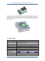


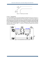
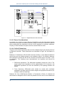
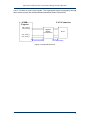


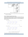

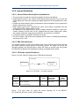
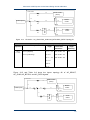
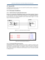
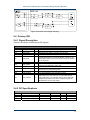
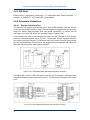
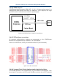

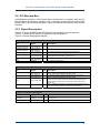
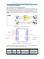
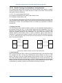
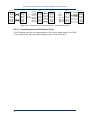

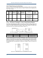

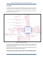

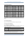
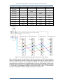
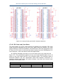
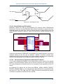


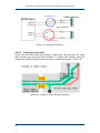
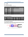
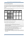

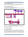

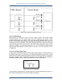

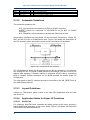
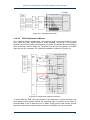
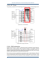

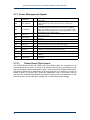
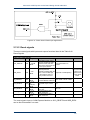
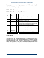

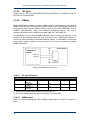


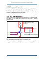
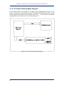


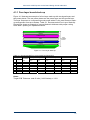

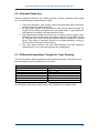

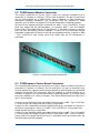


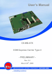
![Invitation to Tender [ANG,PDF]](http://vs1.manualzilla.com/store/data/005809365_1-50c817a2bb68ee8f891e3007a43ef57c-150x150.png)