1
Quartus II Handbook Version 11.1
Volume 3: Verification
101 Innovation Drive
San Jose, CA 95134
www.altera.com
QII5V3-11.1.0
© 2011 Altera Corporation. All rights reserved. ALTERA, ARRIA, CYCLONE, HARDCOPY, MAX, MEGACORE, NIOS, QUARTUS and STRATIX words and logos
are trademarks of Altera Corporation and registered in the U.S. Patent and Trademark Office and in other countries. All other words and logos identified as
ISO
trademarks or service marks are the property of their respective holders as described at www.altera.com/common/legal.html. Altera warrants performance of its
semiconductor products to current specifications in accordance with Altera's standard warranty, but reserves the right to make changes to any products and 9001:2008
services at any time without notice. Altera assumes no responsibility or liability arising out of the application or use of any information, product, or service Registered
described herein except as expressly agreed to in writing by Altera. Altera customers are advised to obtain the latest version of device specifications before relying
on any published information and before placing orders for products or services.
November 2011
Altera Corporation
Quartus II Handbook Version 11.1
Volume 3: Verification
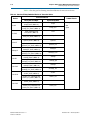
Contents
Chapter Revision Dates . . . . . . . . . . . . . . . . . . . . . . . . . . . . . . . . . . . . . . . . . . . . . . . . . . . . . . . . . . . . . . . . . . . . . xvii
Section I. Simulation
Chapter 1. Simulating Altera Designs
Design Flow . . . . . . . . . . . . . . . . . . . . . . . . . . . . . . . . . . . . . . . . . . . . . . . . . . . . . . . . . . . . . . . . . . . . . . . . . . . . 1–2
Functional Simulation Flow . . . . . . . . . . . . . . . . . . . . . . . . . . . . . . . . . . . . . . . . . . . . . . . . . . . . . . . . . . . . 1–3
Converting Block Design Files (.bdf) to HDL Format (.v/.vhd) . . . . . . . . . . . . . . . . . . . . . . . . . . . . 1–4
Gate-Level Timing Simulation Flow . . . . . . . . . . . . . . . . . . . . . . . . . . . . . . . . . . . . . . . . . . . . . . . . . . . . . 1–5
Simulation Netlist Files . . . . . . . . . . . . . . . . . . . . . . . . . . . . . . . . . . . . . . . . . . . . . . . . . . . . . . . . . . . . . . 1–6
Simulation Library Compiler . . . . . . . . . . . . . . . . . . . . . . . . . . . . . . . . . . . . . . . . . . . . . . . . . . . . . . . . . . . . . . 1–8
Running the Simulation Library Compiler Through the GUI . . . . . . . . . . . . . . . . . . . . . . . . . . . . . . . . 1–8
Running the Simulation Library Compiler from the Command Line . . . . . . . . . . . . . . . . . . . . . . . . . 1–9
Launching the EDA Simulator with the NativeLink Feature . . . . . . . . . . . . . . . . . . . . . . . . . . . . . . . . . . . 1–9
Setting Up the EDA Simulator Execution Path . . . . . . . . . . . . . . . . . . . . . . . . . . . . . . . . . . . . . . . . . . . . 1–9
Configuring NativeLink Settings . . . . . . . . . . . . . . . . . . . . . . . . . . . . . . . . . . . . . . . . . . . . . . . . . . . . . . . 1–10
Setting Up Testbench Files Using the NativeLink Feature . . . . . . . . . . . . . . . . . . . . . . . . . . . . . . . . . . 1–12
Simulating Altera IP Cores . . . . . . . . . . . . . . . . . . . . . . . . . . . . . . . . . . . . . . . . . . . . . . . . . . . . . . . . . . . . . . 1–14
IP Simulation Flows . . . . . . . . . . . . . . . . . . . . . . . . . . . . . . . . . . . . . . . . . . . . . . . . . . . . . . . . . . . . . . . . . . 1–15
IP Variant Directory Structure . . . . . . . . . . . . . . . . . . . . . . . . . . . . . . . . . . . . . . . . . . . . . . . . . . . . . . . . . 1–15
Synthesis Files . . . . . . . . . . . . . . . . . . . . . . . . . . . . . . . . . . . . . . . . . . . . . . . . . . . . . . . . . . . . . . . . . . . . 1–15
Simulation Files . . . . . . . . . . . . . . . . . . . . . . . . . . . . . . . . . . . . . . . . . . . . . . . . . . . . . . . . . . . . . . . . . . . 1–16
Perform Functional Simulation with IP Cores Based on _hw.tcl . . . . . . . . . . . . . . . . . . . . . . . . . . . . 1–17
Mentor Graphics ModelSim Simulation Tcl Script . . . . . . . . . . . . . . . . . . . . . . . . . . . . . . . . . . . . . . 1–18
Synopsys VCS and VCS MX Simulation Shell Script . . . . . . . . . . . . . . . . . . . . . . . . . . . . . . . . . . . . 1–20
Cadence Incisive Enterprise Simulation Shell Script . . . . . . . . . . . . . . . . . . . . . . . . . . . . . . . . . . . . 1–20
Perform Functional Simulation with IP Cores not Based on hw.tcl . . . . . . . . . . . . . . . . . . . . . . . . . . 1–20
Verilog HDL and VHDL IP Functional Simulation Models . . . . . . . . . . . . . . . . . . . . . . . . . . . . . . 1–21
Stratix V Simulation Model Libraries . . . . . . . . . . . . . . . . . . . . . . . . . . . . . . . . . . . . . . . . . . . . . . . . . . . 1–21
Simulating Altera IP Cores Using the Quartus II NativeLink Feature . . . . . . . . . . . . . . . . . . . . . 1–22
Using the Simulation Library Compiler . . . . . . . . . . . . . . . . . . . . . . . . . . . . . . . . . . . . . . . . . . . . . . . 1–22
Running Functional Simulation Using the NativeLink Feature . . . . . . . . . . . . . . . . . . . . . . . . . . . 1–23
Running Gate-Level Timing Simulation Using the NativeLink Feature . . . . . . . . . . . . . . . . . . . . 1–23
Simulating Qsys and SOPC Builder System Designs . . . . . . . . . . . . . . . . . . . . . . . . . . . . . . . . . . . . . . . . 1–24
Document Revision History . . . . . . . . . . . . . . . . . . . . . . . . . . . . . . . . . . . . . . . . . . . . . . . . . . . . . . . . . . . . . 1–25
Chapter 2. Mentor Graphics ModelSim and QuestaSim Support
Software Requirements . . . . . . . . . . . . . . . . . . . . . . . . . . . . . . . . . . . . . . . . . . . . . . . . . . . . . . . . . . . . . . . . . . 2–2
Design Flow with ModelSim-Altera, ModelSim, or QuestaSim Software . . . . . . . . . . . . . . . . . . . . . . . . 2–2
Simulation Libraries . . . . . . . . . . . . . . . . . . . . . . . . . . . . . . . . . . . . . . . . . . . . . . . . . . . . . . . . . . . . . . . . . . . . . 2–3
Precompiled Simulation Libraries in the ModelSim-Altera Software . . . . . . . . . . . . . . . . . . . . . . . . . 2–3
Simulation Library Files in the Quartus II Software . . . . . . . . . . . . . . . . . . . . . . . . . . . . . . . . . . . . . . . . 2–3
Disabling Timing Violation on Registers . . . . . . . . . . . . . . . . . . . . . . . . . . . . . . . . . . . . . . . . . . . . . . . . . 2–3
Simulating with the ModelSim-Altera Software . . . . . . . . . . . . . . . . . . . . . . . . . . . . . . . . . . . . . . . . . . . . . 2–4
Setting Up a Quartus II Project for the ModelSim-Altera Software . . . . . . . . . . . . . . . . . . . . . . . . . . . 2–4
Performing Functional Simulation . . . . . . . . . . . . . . . . . . . . . . . . . . . . . . . . . . . . . . . . . . . . . . . . . . . . . . . 2–4
Performing Post-Synthesis Simulation . . . . . . . . . . . . . . . . . . . . . . . . . . . . . . . . . . . . . . . . . . . . . . . . . . . 2–4
Performing Gate-Level Timing Simulation . . . . . . . . . . . . . . . . . . . . . . . . . . . . . . . . . . . . . . . . . . . . . . . 2–5
November 2011
Altera Corporation
Quartus II Handbook Version 11.1
Volume 3: Verification
iv
Contents
Simulating with the ModelSim and QuestaSim Software . . . . . . . . . . . . . . . . . . . . . . . . . . . . . . . . . . . . . . 2–5
Simulating VHDL or Verilog HDL Designs with the GUI . . . . . . . . . . . . . . . . . . . . . . . . . . . . . . . . . . . 2–5
Functional Simulation . . . . . . . . . . . . . . . . . . . . . . . . . . . . . . . . . . . . . . . . . . . . . . . . . . . . . . . . . . . . . . . 2–6
Post-Synthesis Simulation . . . . . . . . . . . . . . . . . . . . . . . . . . . . . . . . . . . . . . . . . . . . . . . . . . . . . . . . . . . 2–6
Gate-Level Timing Simulation . . . . . . . . . . . . . . . . . . . . . . . . . . . . . . . . . . . . . . . . . . . . . . . . . . . . . . . . 2–7
Simulating VHDL or Verilog HDL Designs with the Command Line . . . . . . . . . . . . . . . . . . . . . . . . . 2–7
Functional Simulation . . . . . . . . . . . . . . . . . . . . . . . . . . . . . . . . . . . . . . . . . . . . . . . . . . . . . . . . . . . . . . . 2–7
Post-Synthesis Simulation . . . . . . . . . . . . . . . . . . . . . . . . . . . . . . . . . . . . . . . . . . . . . . . . . . . . . . . . . . . 2–9
Gate-Level Timing Simulation . . . . . . . . . . . . . . . . . . . . . . . . . . . . . . . . . . . . . . . . . . . . . . . . . . . . . . . 2–11
Passing Parameter Information from Verilog HDL to VHDL . . . . . . . . . . . . . . . . . . . . . . . . . . . . . . . 2–12
Speeding Up Simulation . . . . . . . . . . . . . . . . . . . . . . . . . . . . . . . . . . . . . . . . . . . . . . . . . . . . . . . . . . . . . . 2–12
Simulating Designs that Include Transceivers . . . . . . . . . . . . . . . . . . . . . . . . . . . . . . . . . . . . . . . . . . . . . . 2–12
Functional Simulation . . . . . . . . . . . . . . . . . . . . . . . . . . . . . . . . . . . . . . . . . . . . . . . . . . . . . . . . . . . . . . . . 2–13
ModelSim-Altera . . . . . . . . . . . . . . . . . . . . . . . . . . . . . . . . . . . . . . . . . . . . . . . . . . . . . . . . . . . . . . . . . . 2–13
ModelSim or QuestaSim . . . . . . . . . . . . . . . . . . . . . . . . . . . . . . . . . . . . . . . . . . . . . . . . . . . . . . . . . . . . 2–14
Gate-Level Timing Simulation . . . . . . . . . . . . . . . . . . . . . . . . . . . . . . . . . . . . . . . . . . . . . . . . . . . . . . . . . 2–15
ModelSim-Altera . . . . . . . . . . . . . . . . . . . . . . . . . . . . . . . . . . . . . . . . . . . . . . . . . . . . . . . . . . . . . . . . . . 2–15
ModelSim or QuestaSim . . . . . . . . . . . . . . . . . . . . . . . . . . . . . . . . . . . . . . . . . . . . . . . . . . . . . . . . . . . . 2–15
Transport Delays . . . . . . . . . . . . . . . . . . . . . . . . . . . . . . . . . . . . . . . . . . . . . . . . . . . . . . . . . . . . . . . . . . . . 2–17
Using the NativeLink Feature with ModelSim-Altera, ModelSim, or QuestaSim Software . . . . . . . . 2–17
ModelSim and QuestaSim Error Message Information . . . . . . . . . . . . . . . . . . . . . . . . . . . . . . . . . . . . . . . 2–18
Generating a Timing Value Change Dump File (.vcd) for the PowerPlay Power Analyzer . . . . . . . . 2–18
Viewing a Waveform from a .wlf . . . . . . . . . . . . . . . . . . . . . . . . . . . . . . . . . . . . . . . . . . . . . . . . . . . . . . . . . 2–19
Simulating with ModelSim-Altera Waveform Editor . . . . . . . . . . . . . . . . . . . . . . . . . . . . . . . . . . . . . . . . 2–20
Scripting Support . . . . . . . . . . . . . . . . . . . . . . . . . . . . . . . . . . . . . . . . . . . . . . . . . . . . . . . . . . . . . . . . . . . . . . 2–20
Generating a Post-Synthesis Simulation Netlist for ModelSim and QuestaSim . . . . . . . . . . . . . . . . 2–20
Tcl Commands . . . . . . . . . . . . . . . . . . . . . . . . . . . . . . . . . . . . . . . . . . . . . . . . . . . . . . . . . . . . . . . . . . . . 2–20
Command Prompt . . . . . . . . . . . . . . . . . . . . . . . . . . . . . . . . . . . . . . . . . . . . . . . . . . . . . . . . . . . . . . . . . 2–21
Generating a Gate-Level Timing Simulation Netlist for ModelSim and QuestaSim . . . . . . . . . . . . 2–21
Tcl Commands . . . . . . . . . . . . . . . . . . . . . . . . . . . . . . . . . . . . . . . . . . . . . . . . . . . . . . . . . . . . . . . . . . . . 2–21
Command Line . . . . . . . . . . . . . . . . . . . . . . . . . . . . . . . . . . . . . . . . . . . . . . . . . . . . . . . . . . . . . . . . . . . . 2–22
Software Licensing and Licensing Setup in ModelSim-Altera Subscription Edition . . . . . . . . . . . . . . 2–22
Conclusion . . . . . . . . . . . . . . . . . . . . . . . . . . . . . . . . . . . . . . . . . . . . . . . . . . . . . . . . . . . . . . . . . . . . . . . . . . . . 2–22
Document Revision History . . . . . . . . . . . . . . . . . . . . . . . . . . . . . . . . . . . . . . . . . . . . . . . . . . . . . . . . . . . . . 2–23
Chapter 3. Synopsys VCS and VCS MX Support
Software Requirements . . . . . . . . . . . . . . . . . . . . . . . . . . . . . . . . . . . . . . . . . . . . . . . . . . . . . . . . . . . . . . . . . . 3–1
Using the VCS or VCS MX Software in the Quartus II Design Flow . . . . . . . . . . . . . . . . . . . . . . . . . . . . . 3–1
Compiling Libraries Using the EDA Simulation Library Compiler . . . . . . . . . . . . . . . . . . . . . . . . . . . 3–2
Functional Simulation . . . . . . . . . . . . . . . . . . . . . . . . . . . . . . . . . . . . . . . . . . . . . . . . . . . . . . . . . . . . . . . . . 3–2
Functional Simulation for Verilog HDL and SystemVerilog HDL Designs . . . . . . . . . . . . . . . . . . 3–2
Functional Simulation for VHDL Designs . . . . . . . . . . . . . . . . . . . . . . . . . . . . . . . . . . . . . . . . . . . . . . 3–3
Post-Synthesis Simulation . . . . . . . . . . . . . . . . . . . . . . . . . . . . . . . . . . . . . . . . . . . . . . . . . . . . . . . . . . . . . . 3–4
Post-Synthesis Simulation for Verilog HDL and SystemVerilog HDL Designs . . . . . . . . . . . . . . . 3–4
Post-Synthesis Simulation for VHDL Designs . . . . . . . . . . . . . . . . . . . . . . . . . . . . . . . . . . . . . . . . . . 3–6
Gate-Level Timing Simulation . . . . . . . . . . . . . . . . . . . . . . . . . . . . . . . . . . . . . . . . . . . . . . . . . . . . . . . . . . 3–6
Gate-Level Timing Simulation for Verilog HDL and SystemVerilog HDL Designs . . . . . . . . . . . 3–7
Gate-Level Timing Simulation for VHDL Designs . . . . . . . . . . . . . . . . . . . . . . . . . . . . . . . . . . . . . . . 3–7
Disabling Timing Violation on Registers . . . . . . . . . . . . . . . . . . . . . . . . . . . . . . . . . . . . . . . . . . . . . . . . . 3–7
Performing Functional Simulation Using the Post-Synthesis Netlist . . . . . . . . . . . . . . . . . . . . . . . . . . 3–7
Common VCS and VCS MX Software Compiler Options . . . . . . . . . . . . . . . . . . . . . . . . . . . . . . . . . . . . . . 3–8
Using DVE . . . . . . . . . . . . . . . . . . . . . . . . . . . . . . . . . . . . . . . . . . . . . . . . . . . . . . . . . . . . . . . . . . . . . . . . . . . . . 3–8
Debugging Support Command-Line Interface . . . . . . . . . . . . . . . . . . . . . . . . . . . . . . . . . . . . . . . . . . . . . . . 3–9
Simulating Designs that Include Transceivers . . . . . . . . . . . . . . . . . . . . . . . . . . . . . . . . . . . . . . . . . . . . . . . 3–9
Quartus II Handbook Version 11.1
Volume 3: Verification
November 2011 Altera Corporation
Contents
v
Functional Simulation for Stratix GX Devices . . . . . . . . . . . . . . . . . . . . . . . . . . . . . . . . . . . . . . . . . . . . . 3–9
Gate-Level Timing Simulation for Stratix GX Devices . . . . . . . . . . . . . . . . . . . . . . . . . . . . . . . . . . . . . 3–10
Functional Simulation for Stratix II GX Devices . . . . . . . . . . . . . . . . . . . . . . . . . . . . . . . . . . . . . . . . . . 3–10
Gate-Level Timing Simulation for Stratix II GX Devices . . . . . . . . . . . . . . . . . . . . . . . . . . . . . . . . . . . 3–11
Functional Simulation for Stratix IV GX Devices . . . . . . . . . . . . . . . . . . . . . . . . . . . . . . . . . . . . . . . . . 3–11
Gate-Level Timing Simulation for Stratix IV GX Devices . . . . . . . . . . . . . . . . . . . . . . . . . . . . . . . . . . 3–11
Functional Simulation for Stratix V GX Devices . . . . . . . . . . . . . . . . . . . . . . . . . . . . . . . . . . . . . . . . . . 3–12
Transport Delays . . . . . . . . . . . . . . . . . . . . . . . . . . . . . . . . . . . . . . . . . . . . . . . . . . . . . . . . . . . . . . . . . . . . . . . 3–13
Using NativeLink with the VCS or VCS MX Software . . . . . . . . . . . . . . . . . . . . . . . . . . . . . . . . . . . . . . . 3–13
Generating a Timing .vcd File for the PowerPlay Power Analyzer . . . . . . . . . . . . . . . . . . . . . . . . . . . . . 3–13
Viewing a Waveform from a .vpd or .vcd File . . . . . . . . . . . . . . . . . . . . . . . . . . . . . . . . . . . . . . . . . . . . . . 3–14
Scripting Support . . . . . . . . . . . . . . . . . . . . . . . . . . . . . . . . . . . . . . . . . . . . . . . . . . . . . . . . . . . . . . . . . . . . . . 3–15
Generating a Post-Synthesis Simulation Netlist File for VCS . . . . . . . . . . . . . . . . . . . . . . . . . . . . . . . 3–15
Tcl Commands . . . . . . . . . . . . . . . . . . . . . . . . . . . . . . . . . . . . . . . . . . . . . . . . . . . . . . . . . . . . . . . . . . . . 3–15
Command Prompt . . . . . . . . . . . . . . . . . . . . . . . . . . . . . . . . . . . . . . . . . . . . . . . . . . . . . . . . . . . . . . . . . 3–15
Generating a Gate-Level Timing Simulation Netlist File for VCS . . . . . . . . . . . . . . . . . . . . . . . . . . . 3–15
Tcl Commands . . . . . . . . . . . . . . . . . . . . . . . . . . . . . . . . . . . . . . . . . . . . . . . . . . . . . . . . . . . . . . . . . . . . 3–15
Command Prompt . . . . . . . . . . . . . . . . . . . . . . . . . . . . . . . . . . . . . . . . . . . . . . . . . . . . . . . . . . . . . . . . . 3–15
Conclusion . . . . . . . . . . . . . . . . . . . . . . . . . . . . . . . . . . . . . . . . . . . . . . . . . . . . . . . . . . . . . . . . . . . . . . . . . . . . 3–16
Document Revision History . . . . . . . . . . . . . . . . . . . . . . . . . . . . . . . . . . . . . . . . . . . . . . . . . . . . . . . . . . . . . 3–16
Chapter 4. Cadence Incisive Enterprise Simulator Support
Software Requirements . . . . . . . . . . . . . . . . . . . . . . . . . . . . . . . . . . . . . . . . . . . . . . . . . . . . . . . . . . . . . . . . . . 4–1
Simulation Flow Overview . . . . . . . . . . . . . . . . . . . . . . . . . . . . . . . . . . . . . . . . . . . . . . . . . . . . . . . . . . . . . . . 4–1
Operation Modes . . . . . . . . . . . . . . . . . . . . . . . . . . . . . . . . . . . . . . . . . . . . . . . . . . . . . . . . . . . . . . . . . . . . . 4–2
Quartus II Software and IES Flow Overview . . . . . . . . . . . . . . . . . . . . . . . . . . . . . . . . . . . . . . . . . . . . . . 4–2
Compiling Libraries Using the EDA Simulation Library Compiler . . . . . . . . . . . . . . . . . . . . . . . . . . . 4–3
Functional Simulation . . . . . . . . . . . . . . . . . . . . . . . . . . . . . . . . . . . . . . . . . . . . . . . . . . . . . . . . . . . . . . . . . . . . 4–3
Creating Libraries . . . . . . . . . . . . . . . . . . . . . . . . . . . . . . . . . . . . . . . . . . . . . . . . . . . . . . . . . . . . . . . . . . . . . 4–4
Compiling Source Code . . . . . . . . . . . . . . . . . . . . . . . . . . . . . . . . . . . . . . . . . . . . . . . . . . . . . . . . . . . . . . . . 4–4
Elaborating Your Design . . . . . . . . . . . . . . . . . . . . . . . . . . . . . . . . . . . . . . . . . . . . . . . . . . . . . . . . . . . . . . . 4–5
Simulating Your Design . . . . . . . . . . . . . . . . . . . . . . . . . . . . . . . . . . . . . . . . . . . . . . . . . . . . . . . . . . . . . . . 4–5
Post-Synthesis Simulation . . . . . . . . . . . . . . . . . . . . . . . . . . . . . . . . . . . . . . . . . . . . . . . . . . . . . . . . . . . . . . . . 4–6
Quartus II Simulation Output Files . . . . . . . . . . . . . . . . . . . . . . . . . . . . . . . . . . . . . . . . . . . . . . . . . . . . . . 4–6
Creating Libraries . . . . . . . . . . . . . . . . . . . . . . . . . . . . . . . . . . . . . . . . . . . . . . . . . . . . . . . . . . . . . . . . . . . . . 4–6
Compiling Project Files and Libraries . . . . . . . . . . . . . . . . . . . . . . . . . . . . . . . . . . . . . . . . . . . . . . . . . . . . 4–7
Elaborating Your Design . . . . . . . . . . . . . . . . . . . . . . . . . . . . . . . . . . . . . . . . . . . . . . . . . . . . . . . . . . . . . . . 4–7
Simulating Your Design . . . . . . . . . . . . . . . . . . . . . . . . . . . . . . . . . . . . . . . . . . . . . . . . . . . . . . . . . . . . . . . 4–7
Gate-Level Timing Simulation . . . . . . . . . . . . . . . . . . . . . . . . . . . . . . . . . . . . . . . . . . . . . . . . . . . . . . . . . . . . 4–7
Generating a Gate-Level Timing Simulation Netlist . . . . . . . . . . . . . . . . . . . . . . . . . . . . . . . . . . . . . . . . 4–7
Disabling Timing Violation on Registers . . . . . . . . . . . . . . . . . . . . . . . . . . . . . . . . . . . . . . . . . . . . . . . . . 4–8
Creating Libraries . . . . . . . . . . . . . . . . . . . . . . . . . . . . . . . . . . . . . . . . . . . . . . . . . . . . . . . . . . . . . . . . . . . . . 4–8
Compiling Project Files and Libraries . . . . . . . . . . . . . . . . . . . . . . . . . . . . . . . . . . . . . . . . . . . . . . . . . . . . 4–8
Elaborating Your Design . . . . . . . . . . . . . . . . . . . . . . . . . . . . . . . . . . . . . . . . . . . . . . . . . . . . . . . . . . . . . . . 4–8
Compiling the .sdo File (VHDL Only) in Command-Line Mode . . . . . . . . . . . . . . . . . . . . . . . . . . . 4–9
Compiling the .sdo File (VHDL Only) in GUI Mode . . . . . . . . . . . . . . . . . . . . . . . . . . . . . . . . . . . . . 4–9
Simulating Your Design . . . . . . . . . . . . . . . . . . . . . . . . . . . . . . . . . . . . . . . . . . . . . . . . . . . . . . . . . . . . . . 4–10
Simulating Designs that Include Transceivers . . . . . . . . . . . . . . . . . . . . . . . . . . . . . . . . . . . . . . . . . . . . . . 4–10
Functional Simulation for Stratix GX Devices . . . . . . . . . . . . . . . . . . . . . . . . . . . . . . . . . . . . . . . . . . . . 4–10
Gate-Level Timing Simulation for Stratix GX Devices . . . . . . . . . . . . . . . . . . . . . . . . . . . . . . . . . . . . . 4–11
Functional Simulation for Stratix II GX Devices . . . . . . . . . . . . . . . . . . . . . . . . . . . . . . . . . . . . . . . . . . 4–11
Gate-Level Timing Simulation for Stratix II GX Devices . . . . . . . . . . . . . . . . . . . . . . . . . . . . . . . . . . . 4–13
Functional Simulation for Stratix IV GX Devices . . . . . . . . . . . . . . . . . . . . . . . . . . . . . . . . . . . . . . . . . 4–14
Gate-Level Timing Simulation for Stratix IV GX Devices . . . . . . . . . . . . . . . . . . . . . . . . . . . . . . . . . . 4–15
November 2011
Altera Corporation
Quartus II Handbook Version 11.1
Volume 3: Verification
vi
Contents
Functional Simulation for Stratix V Devices . . . . . . . . . . . . . . . . . . . . . . . . . . . . . . . . . . . . . . . . . . . . . . 4–16
Pulse Reject Delays . . . . . . . . . . . . . . . . . . . . . . . . . . . . . . . . . . . . . . . . . . . . . . . . . . . . . . . . . . . . . . . . . . . 4–16
Using the NativeLink Feature with IES . . . . . . . . . . . . . . . . . . . . . . . . . . . . . . . . . . . . . . . . . . . . . . . . . . . . 4–17
Generating a Timing VCD File for the PowerPlay Power Analyzer . . . . . . . . . . . . . . . . . . . . . . . . . . . . 4–17
Viewing a Waveform from a .trn File . . . . . . . . . . . . . . . . . . . . . . . . . . . . . . . . . . . . . . . . . . . . . . . . . . . . . . 4–18
Scripting Support . . . . . . . . . . . . . . . . . . . . . . . . . . . . . . . . . . . . . . . . . . . . . . . . . . . . . . . . . . . . . . . . . . . . . . 4–19
Generating IES Simulation Output Files . . . . . . . . . . . . . . . . . . . . . . . . . . . . . . . . . . . . . . . . . . . . . . . . . 4–19
Tcl Commands . . . . . . . . . . . . . . . . . . . . . . . . . . . . . . . . . . . . . . . . . . . . . . . . . . . . . . . . . . . . . . . . . . . . 4–19
Command Prompt . . . . . . . . . . . . . . . . . . . . . . . . . . . . . . . . . . . . . . . . . . . . . . . . . . . . . . . . . . . . . . . . . 4–20
Conclusion . . . . . . . . . . . . . . . . . . . . . . . . . . . . . . . . . . . . . . . . . . . . . . . . . . . . . . . . . . . . . . . . . . . . . . . . . . . . 4–20
Document Revision History . . . . . . . . . . . . . . . . . . . . . . . . . . . . . . . . . . . . . . . . . . . . . . . . . . . . . . . . . . . . . 4–20
Chapter 5. Aldec Active-HDL and Riviera-PRO Support
Software Requirements . . . . . . . . . . . . . . . . . . . . . . . . . . . . . . . . . . . . . . . . . . . . . . . . . . . . . . . . . . . . . . . . . . 5–1
Using Active-HDL or Riviera-PRO Software in Quartus II Design Flows . . . . . . . . . . . . . . . . . . . . . . . . 5–2
Simulation Libraries . . . . . . . . . . . . . . . . . . . . . . . . . . . . . . . . . . . . . . . . . . . . . . . . . . . . . . . . . . . . . . . . . . . . . 5–2
Simulation Library Files in the Quartus II Software . . . . . . . . . . . . . . . . . . . . . . . . . . . . . . . . . . . . . . . . 5–2
Compiling Libraries with the EDA Simulation Library Compiler . . . . . . . . . . . . . . . . . . . . . . . . . . . . 5–3
Performing Simulation with the Active-HDL and Riviera-PRO Software . . . . . . . . . . . . . . . . . . . . . . . . 5–3
Functional Simulation . . . . . . . . . . . . . . . . . . . . . . . . . . . . . . . . . . . . . . . . . . . . . . . . . . . . . . . . . . . . . . . . . 5–4
Simulating VHDL Designs with the Active-HDL GUI . . . . . . . . . . . . . . . . . . . . . . . . . . . . . . . . . . . 5–4
Simulating Verilog HDL Designs with the Active-HDL GUI . . . . . . . . . . . . . . . . . . . . . . . . . . . . . . 5–4
Simulating VHDL Designs with Active-HDL from the Command Line . . . . . . . . . . . . . . . . . . . . 5–4
Simulating Verilog HDL Designs with Active-HDL from the Command Line . . . . . . . . . . . . . . . 5–5
Simulating VHDL and Verilog HDL Designs with the Riviera-PRO GUI . . . . . . . . . . . . . . . . . . . 5–6
Simulating VHDL and Verilog HDL Designs with Riviera-PRO from the Command Line . . . . 5–6
Post-Synthesis Simulation . . . . . . . . . . . . . . . . . . . . . . . . . . . . . . . . . . . . . . . . . . . . . . . . . . . . . . . . . . . . . . 5–6
Simulating VHDL Designs with the Active-HDL GUI . . . . . . . . . . . . . . . . . . . . . . . . . . . . . . . . . . . 5–6
Simulating Verilog Designs with the Active-HDL GUI . . . . . . . . . . . . . . . . . . . . . . . . . . . . . . . . . . . 5–7
Simulating VHDL Designs with Active-HDL from the Command Line . . . . . . . . . . . . . . . . . . . . 5–7
Simulating Verilog HDL Designs with Active-HDL from the Command Line . . . . . . . . . . . . . . . 5–8
Simulating VHDL and Verilog HDL Designs with the Riviera-PRO GUI . . . . . . . . . . . . . . . . . . . 5–8
Simulating VHDL and Verilog HDL Designs with Riviera-PRO from the Command Line . . . . 5–9
Gate-Level Timing Simulation . . . . . . . . . . . . . . . . . . . . . . . . . . . . . . . . . . . . . . . . . . . . . . . . . . . . . . . . . . 5–9
Disabling Timing Violation on Registers . . . . . . . . . . . . . . . . . . . . . . . . . . . . . . . . . . . . . . . . . . . . . . . 5–9
Compiling SystemVerilog Files . . . . . . . . . . . . . . . . . . . . . . . . . . . . . . . . . . . . . . . . . . . . . . . . . . . . . . . . . . . . 5–9
Simulating Designs that Include Transceivers . . . . . . . . . . . . . . . . . . . . . . . . . . . . . . . . . . . . . . . . . . . . . . 5–10
Functional Simulation for Stratix II GX Devices . . . . . . . . . . . . . . . . . . . . . . . . . . . . . . . . . . . . . . . . . . 5–10
Performing Functional Simulation in VHDL . . . . . . . . . . . . . . . . . . . . . . . . . . . . . . . . . . . . . . . . . . . 5–11
Performing Functional Simulation in Verilog HDL . . . . . . . . . . . . . . . . . . . . . . . . . . . . . . . . . . . . . 5–11
Gate-Level Timing Simulation for Stratix II GX Devices . . . . . . . . . . . . . . . . . . . . . . . . . . . . . . . . . . . 5–11
Performing Gate-Level Timing Simulation in VHDL . . . . . . . . . . . . . . . . . . . . . . . . . . . . . . . . . . . 5–11
Performing Gate-Level Timing Simulation in Verilog HDL . . . . . . . . . . . . . . . . . . . . . . . . . . . . . . 5–12
Functional Simulation for Stratix GX Devices . . . . . . . . . . . . . . . . . . . . . . . . . . . . . . . . . . . . . . . . . . . . 5–12
Performing Functional Simulation in VHDL . . . . . . . . . . . . . . . . . . . . . . . . . . . . . . . . . . . . . . . . . . . 5–12
Performing Functional Simulation in Verilog HDL . . . . . . . . . . . . . . . . . . . . . . . . . . . . . . . . . . . . . 5–12
Gate-Level Timing Simulation for Stratix GX Devices . . . . . . . . . . . . . . . . . . . . . . . . . . . . . . . . . . . . . 5–13
Performing Gate-Level Timing Simulation in VHDL . . . . . . . . . . . . . . . . . . . . . . . . . . . . . . . . . . . 5–13
Performing Gate-Level Timing Simulation in Verilog HDL . . . . . . . . . . . . . . . . . . . . . . . . . . . . . . 5–13
Functional Simulation for Stratix IV GX Devices . . . . . . . . . . . . . . . . . . . . . . . . . . . . . . . . . . . . . . . . . 5–13
Performing Functional Simulation in VHDL . . . . . . . . . . . . . . . . . . . . . . . . . . . . . . . . . . . . . . . . . . . 5–14
Performing Functional Simulation in Verilog HDL . . . . . . . . . . . . . . . . . . . . . . . . . . . . . . . . . . . . . 5–14
Gate-Level Timing Simulation for Stratix IV GX Devices . . . . . . . . . . . . . . . . . . . . . . . . . . . . . . . . . . 5–14
Performing Gate-Level Timing Simulation in VHDL . . . . . . . . . . . . . . . . . . . . . . . . . . . . . . . . . . . 5–14
Quartus II Handbook Version 11.1
Volume 3: Verification
November 2011 Altera Corporation
Contents
vii
Performing Gate-Level Timing Simulation in Verilog HDL . . . . . . . . . . . . . . . . . . . . . . . . . . . . . . 5–15
Functional Simulation for Stratix V GX Devices . . . . . . . . . . . . . . . . . . . . . . . . . . . . . . . . . . . . . . . . . . 5–15
Performing Functional Simulation in VHDL . . . . . . . . . . . . . . . . . . . . . . . . . . . . . . . . . . . . . . . . . . . 5–15
Performing Functional Simulation in Verilog HDL . . . . . . . . . . . . . . . . . . . . . . . . . . . . . . . . . . . . . 5–16
Transport Delays . . . . . . . . . . . . . . . . . . . . . . . . . . . . . . . . . . . . . . . . . . . . . . . . . . . . . . . . . . . . . . . . . . . . 5–16
Using the NativeLink Feature in Active-HDL or Riviera-PRO Software . . . . . . . . . . . . . . . . . . . . . . . . 5–17
Generating .vcd Files for the PowerPlay Power Analyzer . . . . . . . . . . . . . . . . . . . . . . . . . . . . . . . . . . . . 5–17
Scripting Support . . . . . . . . . . . . . . . . . . . . . . . . . . . . . . . . . . . . . . . . . . . . . . . . . . . . . . . . . . . . . . . . . . . . . . 5–18
Generating a Post-Synthesis Simulation Netlist for Active-HDL or Riviera-PRO . . . . . . . . . . . . . . 5–18
Tcl Commands . . . . . . . . . . . . . . . . . . . . . . . . . . . . . . . . . . . . . . . . . . . . . . . . . . . . . . . . . . . . . . . . . . . . 5–18
Command Line . . . . . . . . . . . . . . . . . . . . . . . . . . . . . . . . . . . . . . . . . . . . . . . . . . . . . . . . . . . . . . . . . . . . 5–18
Generating a Gate-Level Timing Simulation Netlist for Active-HDL or Riviera-PRO . . . . . . . . . . 5–19
Tcl Commands . . . . . . . . . . . . . . . . . . . . . . . . . . . . . . . . . . . . . . . . . . . . . . . . . . . . . . . . . . . . . . . . . . . . 5–19
Command Line . . . . . . . . . . . . . . . . . . . . . . . . . . . . . . . . . . . . . . . . . . . . . . . . . . . . . . . . . . . . . . . . . . . . 5–19
Conclusion . . . . . . . . . . . . . . . . . . . . . . . . . . . . . . . . . . . . . . . . . . . . . . . . . . . . . . . . . . . . . . . . . . . . . . . . . . . . 5–19
Document Revision History . . . . . . . . . . . . . . . . . . . . . . . . . . . . . . . . . . . . . . . . . . . . . . . . . . . . . . . . . . . . . 5–19
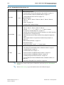
Section II. Timing Analysis
Chapter 6. Timing Analysis Overview
TimeQuest Terminology and Concepts . . . . . . . . . . . . . . . . . . . . . . . . . . . . . . . . . . . . . . . . . . . . . . . . . . . . . 6–1
Timing Netlists and Timing Paths . . . . . . . . . . . . . . . . . . . . . . . . . . . . . . . . . . . . . . . . . . . . . . . . . . . . . . . 6–1
The Timing Netlist . . . . . . . . . . . . . . . . . . . . . . . . . . . . . . . . . . . . . . . . . . . . . . . . . . . . . . . . . . . . . . . . . . 6–2
Timing Paths . . . . . . . . . . . . . . . . . . . . . . . . . . . . . . . . . . . . . . . . . . . . . . . . . . . . . . . . . . . . . . . . . . . . . . . 6–2
Data and Clock Arrival Times . . . . . . . . . . . . . . . . . . . . . . . . . . . . . . . . . . . . . . . . . . . . . . . . . . . . . . . . 6–3
Launch and Latch Edges . . . . . . . . . . . . . . . . . . . . . . . . . . . . . . . . . . . . . . . . . . . . . . . . . . . . . . . . . . . . . 6–4
Clock Setup Check . . . . . . . . . . . . . . . . . . . . . . . . . . . . . . . . . . . . . . . . . . . . . . . . . . . . . . . . . . . . . . . . . . . . 6–5
Clock Hold Check . . . . . . . . . . . . . . . . . . . . . . . . . . . . . . . . . . . . . . . . . . . . . . . . . . . . . . . . . . . . . . . . . . . . . 6–6
Recovery and Removal Time . . . . . . . . . . . . . . . . . . . . . . . . . . . . . . . . . . . . . . . . . . . . . . . . . . . . . . . . . . . 6–7
Multicycle Paths . . . . . . . . . . . . . . . . . . . . . . . . . . . . . . . . . . . . . . . . . . . . . . . . . . . . . . . . . . . . . . . . . . . . . . 6–9
Metastability . . . . . . . . . . . . . . . . . . . . . . . . . . . . . . . . . . . . . . . . . . . . . . . . . . . . . . . . . . . . . . . . . . . . . . . . 6–10
Common Clock Path Pessimism Removal . . . . . . . . . . . . . . . . . . . . . . . . . . . . . . . . . . . . . . . . . . . . . . . 6–10
Clock-As-Data Analysis . . . . . . . . . . . . . . . . . . . . . . . . . . . . . . . . . . . . . . . . . . . . . . . . . . . . . . . . . . . . . . . 6–12
Multicorner Analysis . . . . . . . . . . . . . . . . . . . . . . . . . . . . . . . . . . . . . . . . . . . . . . . . . . . . . . . . . . . . . . . . . 6–14
Document Revision History . . . . . . . . . . . . . . . . . . . . . . . . . . . . . . . . . . . . . . . . . . . . . . . . . . . . . . . . . . . . . 6–15
Chapter 7. The Quartus II TimeQuest Timing Analyzer
Getting Started with the TimeQuest Analyzer . . . . . . . . . . . . . . . . . . . . . . . . . . . . . . . . . . . . . . . . . . . . . . . 7–1
Running the TimeQuest Analyzer . . . . . . . . . . . . . . . . . . . . . . . . . . . . . . . . . . . . . . . . . . . . . . . . . . . . . . . 7–1
Recommended Flow . . . . . . . . . . . . . . . . . . . . . . . . . . . . . . . . . . . . . . . . . . . . . . . . . . . . . . . . . . . . . . . . . . . 7–3
Creating and Setting Up your Design . . . . . . . . . . . . . . . . . . . . . . . . . . . . . . . . . . . . . . . . . . . . . . . . . 7–3
Performing an Initial Compilation . . . . . . . . . . . . . . . . . . . . . . . . . . . . . . . . . . . . . . . . . . . . . . . . . . . . 7–4
Specifying Timing Requirements . . . . . . . . . . . . . . . . . . . . . . . . . . . . . . . . . . . . . . . . . . . . . . . . . . . . . 7–4
Fitting and Timing Analysis with .sdc Files . . . . . . . . . . . . . . . . . . . . . . . . . . . . . . . . . . . . . . . . . . . . 7–5
Performing a Full Compilation . . . . . . . . . . . . . . . . . . . . . . . . . . . . . . . . . . . . . . . . . . . . . . . . . . . . . . . 7–5
Verifying Timing . . . . . . . . . . . . . . . . . . . . . . . . . . . . . . . . . . . . . . . . . . . . . . . . . . . . . . . . . . . . . . . . . . . 7–5
Locating Timing Paths in Other Tools . . . . . . . . . . . . . . . . . . . . . . . . . . . . . . . . . . . . . . . . . . . . . . . . . . . . 7–6
SDC File Precedence . . . . . . . . . . . . . . . . . . . . . . . . . . . . . . . . . . . . . . . . . . . . . . . . . . . . . . . . . . . . . . . . . . . 7–7
Constraining and Analyzing with Tcl Commands . . . . . . . . . . . . . . . . . . . . . . . . . . . . . . . . . . . . . . . . . . . 7–7
Wildcard Characters . . . . . . . . . . . . . . . . . . . . . . . . . . . . . . . . . . . . . . . . . . . . . . . . . . . . . . . . . . . . . . . . . . 7–8
Collection Commands . . . . . . . . . . . . . . . . . . . . . . . . . . . . . . . . . . . . . . . . . . . . . . . . . . . . . . . . . . . . . . . . . 7–8
Adding and Removing Collection Items . . . . . . . . . . . . . . . . . . . . . . . . . . . . . . . . . . . . . . . . . . . . . . . 7–9
Refining Collections with Wildcards . . . . . . . . . . . . . . . . . . . . . . . . . . . . . . . . . . . . . . . . . . . . . . . . . 7–10
November 2011
Altera Corporation
Quartus II Handbook Version 11.1
Volume 3: Verification
viii
Contents
Removing Constraints and Exceptions . . . . . . . . . . . . . . . . . . . . . . . . . . . . . . . . . . . . . . . . . . . . . . . . . . 7–10
Design Constraints: An Example . . . . . . . . . . . . . . . . . . . . . . . . . . . . . . . . . . . . . . . . . . . . . . . . . . . . . . . . . 7–11
Creating Clocks and Clock Constraints . . . . . . . . . . . . . . . . . . . . . . . . . . . . . . . . . . . . . . . . . . . . . . . . . . . . 7–13
Creating Base Clocks . . . . . . . . . . . . . . . . . . . . . . . . . . . . . . . . . . . . . . . . . . . . . . . . . . . . . . . . . . . . . . . . . 7–13
Creating Virtual Clocks . . . . . . . . . . . . . . . . . . . . . . . . . . . . . . . . . . . . . . . . . . . . . . . . . . . . . . . . . . . . . . . 7–14
Creating Multifrequency Clocks . . . . . . . . . . . . . . . . . . . . . . . . . . . . . . . . . . . . . . . . . . . . . . . . . . . . . . . 7–15
Creating Generated Clocks . . . . . . . . . . . . . . . . . . . . . . . . . . . . . . . . . . . . . . . . . . . . . . . . . . . . . . . . . . . . 7–16
Automatically Detecting Clocks and Creating Default Clock Constraints . . . . . . . . . . . . . . . . . . . . 7–18
Deriving PLL Clocks . . . . . . . . . . . . . . . . . . . . . . . . . . . . . . . . . . . . . . . . . . . . . . . . . . . . . . . . . . . . . . . . . 7–19
Creating Clock Groups . . . . . . . . . . . . . . . . . . . . . . . . . . . . . . . . . . . . . . . . . . . . . . . . . . . . . . . . . . . . . . . 7–20
Exclusive Clock Groups . . . . . . . . . . . . . . . . . . . . . . . . . . . . . . . . . . . . . . . . . . . . . . . . . . . . . . . . . . . . 7–20
Asynchronous Clock Groups . . . . . . . . . . . . . . . . . . . . . . . . . . . . . . . . . . . . . . . . . . . . . . . . . . . . . . . . 7–21
Accounting for Clock Effect Characteristics . . . . . . . . . . . . . . . . . . . . . . . . . . . . . . . . . . . . . . . . . . . . . . 7–21
Clock Latency . . . . . . . . . . . . . . . . . . . . . . . . . . . . . . . . . . . . . . . . . . . . . . . . . . . . . . . . . . . . . . . . . . . . . 7–21
Clock Uncertainty . . . . . . . . . . . . . . . . . . . . . . . . . . . . . . . . . . . . . . . . . . . . . . . . . . . . . . . . . . . . . . . . . 7–22
I/O Interface Uncertainty . . . . . . . . . . . . . . . . . . . . . . . . . . . . . . . . . . . . . . . . . . . . . . . . . . . . . . . . . . . 7–22
Creating I/O Requirements . . . . . . . . . . . . . . . . . . . . . . . . . . . . . . . . . . . . . . . . . . . . . . . . . . . . . . . . . . . . . . 7–24
Input Constraints . . . . . . . . . . . . . . . . . . . . . . . . . . . . . . . . . . . . . . . . . . . . . . . . . . . . . . . . . . . . . . . . . . . . 7–24
Output Constraints . . . . . . . . . . . . . . . . . . . . . . . . . . . . . . . . . . . . . . . . . . . . . . . . . . . . . . . . . . . . . . . . . . . 7–25
Creating Delay and Skew Constraints . . . . . . . . . . . . . . . . . . . . . . . . . . . . . . . . . . . . . . . . . . . . . . . . . . . . . 7–26
Net Delay . . . . . . . . . . . . . . . . . . . . . . . . . . . . . . . . . . . . . . . . . . . . . . . . . . . . . . . . . . . . . . . . . . . . . . . . . . . 7–26
Advanced I/O Timing and Board Trace Model Delay . . . . . . . . . . . . . . . . . . . . . . . . . . . . . . . . . . . . . 7–26
Maximum Skew . . . . . . . . . . . . . . . . . . . . . . . . . . . . . . . . . . . . . . . . . . . . . . . . . . . . . . . . . . . . . . . . . . . . . 7–27
Creating Timing Exceptions . . . . . . . . . . . . . . . . . . . . . . . . . . . . . . . . . . . . . . . . . . . . . . . . . . . . . . . . . . . . . 7–27
Precedence . . . . . . . . . . . . . . . . . . . . . . . . . . . . . . . . . . . . . . . . . . . . . . . . . . . . . . . . . . . . . . . . . . . . . . . . . . 7–27
False Paths . . . . . . . . . . . . . . . . . . . . . . . . . . . . . . . . . . . . . . . . . . . . . . . . . . . . . . . . . . . . . . . . . . . . . . . . . . 7–27
Minimum and Maximum Delays . . . . . . . . . . . . . . . . . . . . . . . . . . . . . . . . . . . . . . . . . . . . . . . . . . . . . . . 7–28
Delay Annotation . . . . . . . . . . . . . . . . . . . . . . . . . . . . . . . . . . . . . . . . . . . . . . . . . . . . . . . . . . . . . . . . . . . . 7–29
Multicycle Paths . . . . . . . . . . . . . . . . . . . . . . . . . . . . . . . . . . . . . . . . . . . . . . . . . . . . . . . . . . . . . . . . . . . . . 7–29
Creating Multicycle Exceptions . . . . . . . . . . . . . . . . . . . . . . . . . . . . . . . . . . . . . . . . . . . . . . . . . . . . . . . . 7–30
Multicycle Clock Setup Check and Hold Check Analysis . . . . . . . . . . . . . . . . . . . . . . . . . . . . . . . . . . 7–30
Multicycle Clock Setup . . . . . . . . . . . . . . . . . . . . . . . . . . . . . . . . . . . . . . . . . . . . . . . . . . . . . . . . . . . . . 7–31
Multicycle Clock Hold . . . . . . . . . . . . . . . . . . . . . . . . . . . . . . . . . . . . . . . . . . . . . . . . . . . . . . . . . . . . . 7–32
Examples of Basic Multicycle Exceptions . . . . . . . . . . . . . . . . . . . . . . . . . . . . . . . . . . . . . . . . . . . . . . . . 7–34
Default Settings . . . . . . . . . . . . . . . . . . . . . . . . . . . . . . . . . . . . . . . . . . . . . . . . . . . . . . . . . . . . . . . . . . . 7–35
End Multicycle Setup = 2 and End Multicycle Hold = 0 . . . . . . . . . . . . . . . . . . . . . . . . . . . . . . . . . 7–37
End Multicycle Setup = 1 and End Multicycle Hold = 1 . . . . . . . . . . . . . . . . . . . . . . . . . . . . . . . . . 7–40
End Multicycle Setup = 2 and End Multicycle Hold = 1 . . . . . . . . . . . . . . . . . . . . . . . . . . . . . . . . . 7–43
Start Multicycle Setup = 2 and Start Multicycle Hold = 0 . . . . . . . . . . . . . . . . . . . . . . . . . . . . . . . . 7–46
Start Multicycle Setup = 1 and Start Multicycle Hold = 1 . . . . . . . . . . . . . . . . . . . . . . . . . . . . . . . . 7–49
Start Multicycle Setup = 2 and Start Multicycle Hold = 1 . . . . . . . . . . . . . . . . . . . . . . . . . . . . . . . . 7–52
Application of Multicycle Exceptions . . . . . . . . . . . . . . . . . . . . . . . . . . . . . . . . . . . . . . . . . . . . . . . . . . . 7–55
Same Frequency Clocks with Destination Clock Offset . . . . . . . . . . . . . . . . . . . . . . . . . . . . . . . . . . 7–55
The Destination Clock Frequency is a Multiple of the Source Clock Frequency . . . . . . . . . . . . . 7–57
The Destination Clock Frequency is a Multiple of the Source Clock Frequency
with an Offset . . . . . . . . . . . . . . . . . . . . . . . . . . . . . . . . . . . . . . . . . . . . . . . . . . . . . . . . . . . . . . . . . . . . . 7–60
The Source Clock Frequency is a Multiple of the Destination Clock Frequency . . . . . . . . . . . . . 7–62
The Source Clock Frequency is a Multiple of the Destination Clock Frequency
with an Offset . . . . . . . . . . . . . . . . . . . . . . . . . . . . . . . . . . . . . . . . . . . . . . . . . . . . . . . . . . . . . . . . . . . . . 7–64
Timing Reports . . . . . . . . . . . . . . . . . . . . . . . . . . . . . . . . . . . . . . . . . . . . . . . . . . . . . . . . . . . . . . . . . . . . . . . . 7–67
Document Revision History . . . . . . . . . . . . . . . . . . . . . . . . . . . . . . . . . . . . . . . . . . . . . . . . . . . . . . . . . . . . . 7–68
Quartus II Handbook Version 11.1
Volume 3: Verification
November 2011 Altera Corporation
Contents
ix
Section III. Power Estimation and Analysis
Chapter 8. PowerPlay Power Analysis
Types of Power Analyses . . . . . . . . . . . . . . . . . . . . . . . . . . . . . . . . . . . . . . . . . . . . . . . . . . . . . . . . . . . . . . . . . 8–2
Factors Affecting Power Consumption . . . . . . . . . . . . . . . . . . . . . . . . . . . . . . . . . . . . . . . . . . . . . . . . . . . . . 8–2
Device Selection . . . . . . . . . . . . . . . . . . . . . . . . . . . . . . . . . . . . . . . . . . . . . . . . . . . . . . . . . . . . . . . . . . . . . . 8–2
Environmental Conditions . . . . . . . . . . . . . . . . . . . . . . . . . . . . . . . . . . . . . . . . . . . . . . . . . . . . . . . . . . . . . 8–3
Airflow . . . . . . . . . . . . . . . . . . . . . . . . . . . . . . . . . . . . . . . . . . . . . . . . . . . . . . . . . . . . . . . . . . . . . . . . . . . 8–3
Heat Sink and Thermal Compound . . . . . . . . . . . . . . . . . . . . . . . . . . . . . . . . . . . . . . . . . . . . . . . . . . . 8–3
Junction Temperature . . . . . . . . . . . . . . . . . . . . . . . . . . . . . . . . . . . . . . . . . . . . . . . . . . . . . . . . . . . . . . . 8–3
Board Thermal Model . . . . . . . . . . . . . . . . . . . . . . . . . . . . . . . . . . . . . . . . . . . . . . . . . . . . . . . . . . . . . . . 8–3
Device Resource Usage . . . . . . . . . . . . . . . . . . . . . . . . . . . . . . . . . . . . . . . . . . . . . . . . . . . . . . . . . . . . . . . . 8–4
Number, Type, and Loading of I/O Pins . . . . . . . . . . . . . . . . . . . . . . . . . . . . . . . . . . . . . . . . . . . . . . . 8–4
Number and Type of Logic Elements, Multiplier Elements, and RAM Blocks . . . . . . . . . . . . . . . 8–4
Number and Type of Global Signals . . . . . . . . . . . . . . . . . . . . . . . . . . . . . . . . . . . . . . . . . . . . . . . . . . . 8–4
Signal Activities . . . . . . . . . . . . . . . . . . . . . . . . . . . . . . . . . . . . . . . . . . . . . . . . . . . . . . . . . . . . . . . . . . . . . . 8–4
Creating PowerPlay EPE Spreadsheets . . . . . . . . . . . . . . . . . . . . . . . . . . . . . . . . . . . . . . . . . . . . . . . . . . . . . 8–5
PowerPlay EPE File Generator Compilation Report . . . . . . . . . . . . . . . . . . . . . . . . . . . . . . . . . . . . . . . . 8–6
PowerPlay Power Analyzer Flow . . . . . . . . . . . . . . . . . . . . . . . . . . . . . . . . . . . . . . . . . . . . . . . . . . . . . . . . . . 8–8
Operating Settings and Conditions . . . . . . . . . . . . . . . . . . . . . . . . . . . . . . . . . . . . . . . . . . . . . . . . . . . . . . 8–8
Signal Activities Data Sources . . . . . . . . . . . . . . . . . . . . . . . . . . . . . . . . . . . . . . . . . . . . . . . . . . . . . . . . . . 8–9
Simulation Results . . . . . . . . . . . . . . . . . . . . . . . . . . . . . . . . . . . . . . . . . . . . . . . . . . . . . . . . . . . . . . . . . . 8–9
Using Simulation Files in Modular Design Flows . . . . . . . . . . . . . . . . . . . . . . . . . . . . . . . . . . . . . . . . . . . 8–11
Complete Design Simulation . . . . . . . . . . . . . . . . . . . . . . . . . . . . . . . . . . . . . . . . . . . . . . . . . . . . . . . . . . 8–12
Modular Design Simulation . . . . . . . . . . . . . . . . . . . . . . . . . . . . . . . . . . . . . . . . . . . . . . . . . . . . . . . . . . . 8–12
Multiple Simulations on the Same Entity . . . . . . . . . . . . . . . . . . . . . . . . . . . . . . . . . . . . . . . . . . . . . . . . 8–13
Overlapping Simulations . . . . . . . . . . . . . . . . . . . . . . . . . . . . . . . . . . . . . . . . . . . . . . . . . . . . . . . . . . . . . 8–13
Partial Simulations . . . . . . . . . . . . . . . . . . . . . . . . . . . . . . . . . . . . . . . . . . . . . . . . . . . . . . . . . . . . . . . . . . . 8–14
Node Name Matching Considerations . . . . . . . . . . . . . . . . . . . . . . . . . . . . . . . . . . . . . . . . . . . . . . . . . . 8–14
Glitch Filtering . . . . . . . . . . . . . . . . . . . . . . . . . . . . . . . . . . . . . . . . . . . . . . . . . . . . . . . . . . . . . . . . . . . . . . 8–14
Node and Entity Assignments . . . . . . . . . . . . . . . . . . . . . . . . . . . . . . . . . . . . . . . . . . . . . . . . . . . . . . . . . 8–16
Timing Assignments to Clock Nodes . . . . . . . . . . . . . . . . . . . . . . . . . . . . . . . . . . . . . . . . . . . . . . . . . 8–17
Default Toggle Rate Assignment . . . . . . . . . . . . . . . . . . . . . . . . . . . . . . . . . . . . . . . . . . . . . . . . . . . . . . . 8–17
Vectorless Estimation . . . . . . . . . . . . . . . . . . . . . . . . . . . . . . . . . . . . . . . . . . . . . . . . . . . . . . . . . . . . . . . . . 8–17
Using the PowerPlay Power Analyzer . . . . . . . . . . . . . . . . . . . . . . . . . . . . . . . . . . . . . . . . . . . . . . . . . . . . . 8–17
Common Analysis Flows . . . . . . . . . . . . . . . . . . . . . . . . . . . . . . . . . . . . . . . . . . . . . . . . . . . . . . . . . . . . . 8–18
Signal Activities from Full Post-Fit Netlist (Timing) Simulation . . . . . . . . . . . . . . . . . . . . . . . . . . 8–18
Signal Activities from Full Post-Fit Netlist (Zero Delay) Simulation . . . . . . . . . . . . . . . . . . . . . . . 8–18
Signal Activities from RTL (Functional) Simulation, Supplemented by Vectorless Estimation 8–18
Signal Activities from Vectorless Estimation and User-Supplied Input Pin Activities . . . . . . . . 8–18
Signal Activities from User Defaults Only . . . . . . . . . . . . . . . . . . . . . . . . . . . . . . . . . . . . . . . . . . . . . 8–18
Generating a .vcd . . . . . . . . . . . . . . . . . . . . . . . . . . . . . . . . . . . . . . . . . . . . . . . . . . . . . . . . . . . . . . . . . . . . 8–19
Generating a .vcd from ModelSim Software . . . . . . . . . . . . . . . . . . . . . . . . . . . . . . . . . . . . . . . . . . . 8–20
Generating a .vcd from Full Post-Fit Netlist (Zero Delay) Simulation . . . . . . . . . . . . . . . . . . . . . 8–20
Running the PowerPlay Power Analyzer Using the Quartus II GUI . . . . . . . . . . . . . . . . . . . . . . . . . 8–21
PowerPlay Power Analyzer Compilation Report . . . . . . . . . . . . . . . . . . . . . . . . . . . . . . . . . . . . . . . . . 8–21
Summary . . . . . . . . . . . . . . . . . . . . . . . . . . . . . . . . . . . . . . . . . . . . . . . . . . . . . . . . . . . . . . . . . . . . . . . . . 8–21
Settings . . . . . . . . . . . . . . . . . . . . . . . . . . . . . . . . . . . . . . . . . . . . . . . . . . . . . . . . . . . . . . . . . . . . . . . . . . 8–21
Simulation Files Read . . . . . . . . . . . . . . . . . . . . . . . . . . . . . . . . . . . . . . . . . . . . . . . . . . . . . . . . . . . . . . 8–21
Operating Conditions Used . . . . . . . . . . . . . . . . . . . . . . . . . . . . . . . . . . . . . . . . . . . . . . . . . . . . . . . . . 8–22
Thermal Power Dissipated by Block . . . . . . . . . . . . . . . . . . . . . . . . . . . . . . . . . . . . . . . . . . . . . . . . . . 8–22
Thermal Power Dissipation by Block Type (Device Resource Type) . . . . . . . . . . . . . . . . . . . . . . . 8–22
Thermal Power Dissipation by Hierarchy . . . . . . . . . . . . . . . . . . . . . . . . . . . . . . . . . . . . . . . . . . . . . 8–22
November 2011
Altera Corporation
Quartus II Handbook Version 11.1
Volume 3: Verification
x
Contents
Core Dynamic Thermal Power Dissipation by Clock Domain . . . . . . . . . . . . . . . . . . . . . . . . . . . . 8–22
Current Drawn from Voltage Supplies . . . . . . . . . . . . . . . . . . . . . . . . . . . . . . . . . . . . . . . . . . . . . . . 8–22
Confidence Metric Details . . . . . . . . . . . . . . . . . . . . . . . . . . . . . . . . . . . . . . . . . . . . . . . . . . . . . . . . . . 8–23
Signal Activities . . . . . . . . . . . . . . . . . . . . . . . . . . . . . . . . . . . . . . . . . . . . . . . . . . . . . . . . . . . . . . . . . . . 8–23
Messages . . . . . . . . . . . . . . . . . . . . . . . . . . . . . . . . . . . . . . . . . . . . . . . . . . . . . . . . . . . . . . . . . . . . . . . . . 8–23
Specific Rules for Reporting . . . . . . . . . . . . . . . . . . . . . . . . . . . . . . . . . . . . . . . . . . . . . . . . . . . . . . . . . 8–23
Scripting Support . . . . . . . . . . . . . . . . . . . . . . . . . . . . . . . . . . . . . . . . . . . . . . . . . . . . . . . . . . . . . . . . . . . . 8–23
Running the PowerPlay Power Analyzer from the Command–Line . . . . . . . . . . . . . . . . . . . . . . 8–24
Conclusion . . . . . . . . . . . . . . . . . . . . . . . . . . . . . . . . . . . . . . . . . . . . . . . . . . . . . . . . . . . . . . . . . . . . . . . . . . . . 8–25
Document Revision History . . . . . . . . . . . . . . . . . . . . . . . . . . . . . . . . . . . . . . . . . . . . . . . . . . . . . . . . . . . . . 8–25
Section IV. System Debugging Tools
Chapter 9. System Debugging Tools Overview
System Debugging Tools . . . . . . . . . . . . . . . . . . . . . . . . . . . . . . . . . . . . . . . . . . . . . . . . . . . . . . . . . . . . . . . . . 9–1
Analysis Tools for RTL Nodes . . . . . . . . . . . . . . . . . . . . . . . . . . . . . . . . . . . . . . . . . . . . . . . . . . . . . . . . . . 9–4
Resource Usage . . . . . . . . . . . . . . . . . . . . . . . . . . . . . . . . . . . . . . . . . . . . . . . . . . . . . . . . . . . . . . . . . . . . 9–4
Pin Usage . . . . . . . . . . . . . . . . . . . . . . . . . . . . . . . . . . . . . . . . . . . . . . . . . . . . . . . . . . . . . . . . . . . . . . . . . 9–5
Usability Enhancements . . . . . . . . . . . . . . . . . . . . . . . . . . . . . . . . . . . . . . . . . . . . . . . . . . . . . . . . . . . . . 9–6
Stimulus-Capable Tools . . . . . . . . . . . . . . . . . . . . . . . . . . . . . . . . . . . . . . . . . . . . . . . . . . . . . . . . . . . . . . . . 9–8
In-System Sources and Probes . . . . . . . . . . . . . . . . . . . . . . . . . . . . . . . . . . . . . . . . . . . . . . . . . . . . . . . . 9–8
In-System Memory Content Editor . . . . . . . . . . . . . . . . . . . . . . . . . . . . . . . . . . . . . . . . . . . . . . . . . . . . 9–8
Virtual JTAG Interface Megafunction . . . . . . . . . . . . . . . . . . . . . . . . . . . . . . . . . . . . . . . . . . . . . . . . . . 9–9
System Console . . . . . . . . . . . . . . . . . . . . . . . . . . . . . . . . . . . . . . . . . . . . . . . . . . . . . . . . . . . . . . . . . . . . 9–9
Conclusion . . . . . . . . . . . . . . . . . . . . . . . . . . . . . . . . . . . . . . . . . . . . . . . . . . . . . . . . . . . . . . . . . . . . . . . . . . . . . 9–9
Document Revision History . . . . . . . . . . . . . . . . . . . . . . . . . . . . . . . . . . . . . . . . . . . . . . . . . . . . . . . . . . . . . 9–10
Chapter 10. Analyzing and Debugging Designs with the System Console
Introduction . . . . . . . . . . . . . . . . . . . . . . . . . . . . . . . . . . . . . . . . . . . . . . . . . . . . . . . . . . . . . . . . . . . . . . . . . . . 10–1
System Console Overview . . . . . . . . . . . . . . . . . . . . . . . . . . . . . . . . . . . . . . . . . . . . . . . . . . . . . . . . . . . . . . . 10–2
Finding and Referring To Services . . . . . . . . . . . . . . . . . . . . . . . . . . . . . . . . . . . . . . . . . . . . . . . . . . . . . . 10–2
Accessing Services . . . . . . . . . . . . . . . . . . . . . . . . . . . . . . . . . . . . . . . . . . . . . . . . . . . . . . . . . . . . . . . . . . . 10–2
Applying Services . . . . . . . . . . . . . . . . . . . . . . . . . . . . . . . . . . . . . . . . . . . . . . . . . . . . . . . . . . . . . . . . . . . . 10–3
Setting Up the System Console . . . . . . . . . . . . . . . . . . . . . . . . . . . . . . . . . . . . . . . . . . . . . . . . . . . . . . . . . . . 10–3
Interactive Help . . . . . . . . . . . . . . . . . . . . . . . . . . . . . . . . . . . . . . . . . . . . . . . . . . . . . . . . . . . . . . . . . . . . . . . . 10–3
Using the System Console . . . . . . . . . . . . . . . . . . . . . . . . . . . . . . . . . . . . . . . . . . . . . . . . . . . . . . . . . . . . . . . 10–4
Qsys and SOPC Builder Communications . . . . . . . . . . . . . . . . . . . . . . . . . . . . . . . . . . . . . . . . . . . . . . . 10–4
Console Commands . . . . . . . . . . . . . . . . . . . . . . . . . . . . . . . . . . . . . . . . . . . . . . . . . . . . . . . . . . . . . . . . . . 10–6
Plugins . . . . . . . . . . . . . . . . . . . . . . . . . . . . . . . . . . . . . . . . . . . . . . . . . . . . . . . . . . . . . . . . . . . . . . . . . . . . . 10–9
Design Service Commands . . . . . . . . . . . . . . . . . . . . . . . . . . . . . . . . . . . . . . . . . . . . . . . . . . . . . . . . . . . . 10–9
Data Pattern Generator Commands . . . . . . . . . . . . . . . . . . . . . . . . . . . . . . . . . . . . . . . . . . . . . . . . . . . 10–10
Data Pattern Checker Commands . . . . . . . . . . . . . . . . . . . . . . . . . . . . . . . . . . . . . . . . . . . . . . . . . . . . . 10–11
Programmable Logic Device (PLD) Commands . . . . . . . . . . . . . . . . . . . . . . . . . . . . . . . . . . . . . . . . . 10–11
Board Bring-Up Commands . . . . . . . . . . . . . . . . . . . . . . . . . . . . . . . . . . . . . . . . . . . . . . . . . . . . . . . . . . 10–12
JTAG Debug Commands . . . . . . . . . . . . . . . . . . . . . . . . . . . . . . . . . . . . . . . . . . . . . . . . . . . . . . . . . . 10–13
Clock and Reset Signal Commands . . . . . . . . . . . . . . . . . . . . . . . . . . . . . . . . . . . . . . . . . . . . . . . . . 10–13
Avalon-MM Commands . . . . . . . . . . . . . . . . . . . . . . . . . . . . . . . . . . . . . . . . . . . . . . . . . . . . . . . . . . . 10–13
Bytestream Commands . . . . . . . . . . . . . . . . . . . . . . . . . . . . . . . . . . . . . . . . . . . . . . . . . . . . . . . . . . . . 10–14
SLD Commands . . . . . . . . . . . . . . . . . . . . . . . . . . . . . . . . . . . . . . . . . . . . . . . . . . . . . . . . . . . . . . . . . . 10–14
Claim Values for Claim Services . . . . . . . . . . . . . . . . . . . . . . . . . . . . . . . . . . . . . . . . . . . . . . . . . . . . 10–14
Processor Commands . . . . . . . . . . . . . . . . . . . . . . . . . . . . . . . . . . . . . . . . . . . . . . . . . . . . . . . . . . . . . . . 10–15
Bytestream Commands . . . . . . . . . . . . . . . . . . . . . . . . . . . . . . . . . . . . . . . . . . . . . . . . . . . . . . . . . . . . . . 10–16
Transceiver Toolkit Commands . . . . . . . . . . . . . . . . . . . . . . . . . . . . . . . . . . . . . . . . . . . . . . . . . . . . . . . 10–16
Quartus II Handbook Version 11.1
Volume 3: Verification
November 2011 Altera Corporation
Contents
xi
In-System Sources and Probes Commands . . . . . . . . . . . . . . . . . . . . . . . . . . . . . . . . . . . . . . . . . . . . . 10–21
Monitor Commands . . . . . . . . . . . . . . . . . . . . . . . . . . . . . . . . . . . . . . . . . . . . . . . . . . . . . . . . . . . . . . . . . 10–22
Dashboard Commands . . . . . . . . . . . . . . . . . . . . . . . . . . . . . . . . . . . . . . . . . . . . . . . . . . . . . . . . . . . . . . 10–25
Specifying Widgets . . . . . . . . . . . . . . . . . . . . . . . . . . . . . . . . . . . . . . . . . . . . . . . . . . . . . . . . . . . . . . . 10–26
Customizing Widgets . . . . . . . . . . . . . . . . . . . . . . . . . . . . . . . . . . . . . . . . . . . . . . . . . . . . . . . . . . . . . 10–27
Assigning Dashboard Widget Properties . . . . . . . . . . . . . . . . . . . . . . . . . . . . . . . . . . . . . . . . . . . . . 10–27
System Console Examples . . . . . . . . . . . . . . . . . . . . . . . . . . . . . . . . . . . . . . . . . . . . . . . . . . . . . . . . . . . . . . 10–31
LED Light Show Example . . . . . . . . . . . . . . . . . . . . . . . . . . . . . . . . . . . . . . . . . . . . . . . . . . . . . . . . . . . . 10–32
Creating a Simple Dashboard . . . . . . . . . . . . . . . . . . . . . . . . . . . . . . . . . . . . . . . . . . . . . . . . . . . . . . . . . 10–33
Loading and Linking a Design . . . . . . . . . . . . . . . . . . . . . . . . . . . . . . . . . . . . . . . . . . . . . . . . . . . . . . . . 10–35
JTAG Examples . . . . . . . . . . . . . . . . . . . . . . . . . . . . . . . . . . . . . . . . . . . . . . . . . . . . . . . . . . . . . . . . . . . . . 10–36
Verify JTAG Chain . . . . . . . . . . . . . . . . . . . . . . . . . . . . . . . . . . . . . . . . . . . . . . . . . . . . . . . . . . . . . . . . 10–36
Verify Clock . . . . . . . . . . . . . . . . . . . . . . . . . . . . . . . . . . . . . . . . . . . . . . . . . . . . . . . . . . . . . . . . . . . . . 10–37
Checksum Example . . . . . . . . . . . . . . . . . . . . . . . . . . . . . . . . . . . . . . . . . . . . . . . . . . . . . . . . . . . . . . . . . 10–38
Nios II Processor Example . . . . . . . . . . . . . . . . . . . . . . . . . . . . . . . . . . . . . . . . . . . . . . . . . . . . . . . . . . . 10–41
On-Board USB Blaster II Support . . . . . . . . . . . . . . . . . . . . . . . . . . . . . . . . . . . . . . . . . . . . . . . . . . . . . . . . 10–42
Device Support . . . . . . . . . . . . . . . . . . . . . . . . . . . . . . . . . . . . . . . . . . . . . . . . . . . . . . . . . . . . . . . . . . . . . . . 10–42
Conclusion . . . . . . . . . . . . . . . . . . . . . . . . . . . . . . . . . . . . . . . . . . . . . . . . . . . . . . . . . . . . . . . . . . . . . . . . . . . 10–42
Document Revision History . . . . . . . . . . . . . . . . . . . . . . . . . . . . . . . . . . . . . . . . . . . . . . . . . . . . . . . . . . . . 10–43
Chapter 11. Transceiver Link Debugging Using the System Console
Transceiver Toolkit Overview . . . . . . . . . . . . . . . . . . . . . . . . . . . . . . . . . . . . . . . . . . . . . . . . . . . . . . . . . . . . 11–1
Transceiver Toolkit User Interface . . . . . . . . . . . . . . . . . . . . . . . . . . . . . . . . . . . . . . . . . . . . . . . . . . . . . . 11–2
Transceiver Auto Sweep . . . . . . . . . . . . . . . . . . . . . . . . . . . . . . . . . . . . . . . . . . . . . . . . . . . . . . . . . . . . 11–2
Transceiver EyeQ . . . . . . . . . . . . . . . . . . . . . . . . . . . . . . . . . . . . . . . . . . . . . . . . . . . . . . . . . . . . . . . . . . 11–2
Control Links . . . . . . . . . . . . . . . . . . . . . . . . . . . . . . . . . . . . . . . . . . . . . . . . . . . . . . . . . . . . . . . . . . . . . 11–2
Transceiver Link Debugging Design Examples . . . . . . . . . . . . . . . . . . . . . . . . . . . . . . . . . . . . . . . . . . . . . 11–3
Setting Up Tests for Link Debugging . . . . . . . . . . . . . . . . . . . . . . . . . . . . . . . . . . . . . . . . . . . . . . . . . . . 11–3
Custom PHY IP Core . . . . . . . . . . . . . . . . . . . . . . . . . . . . . . . . . . . . . . . . . . . . . . . . . . . . . . . . . . . . . . . 11–5
Transceiver Reconfiguration Controller . . . . . . . . . . . . . . . . . . . . . . . . . . . . . . . . . . . . . . . . . . . . . . . 11–5
Low Latency PHY IP Core . . . . . . . . . . . . . . . . . . . . . . . . . . . . . . . . . . . . . . . . . . . . . . . . . . . . . . . . . . 11–6
Avalon-ST Data Pattern Generator . . . . . . . . . . . . . . . . . . . . . . . . . . . . . . . . . . . . . . . . . . . . . . . . . . . 11–6
Data Checker . . . . . . . . . . . . . . . . . . . . . . . . . . . . . . . . . . . . . . . . . . . . . . . . . . . . . . . . . . . . . . . . . . . . . 11–7
Compiling Design Examples . . . . . . . . . . . . . . . . . . . . . . . . . . . . . . . . . . . . . . . . . . . . . . . . . . . . . . . . . . 11–8
Changing Pin Assignments . . . . . . . . . . . . . . . . . . . . . . . . . . . . . . . . . . . . . . . . . . . . . . . . . . . . . . . . . . . . 11–8
Transceiver Toolkit Link Test Setup . . . . . . . . . . . . . . . . . . . . . . . . . . . . . . . . . . . . . . . . . . . . . . . . . . . . . . . 11–9
Loading the Project in System Console . . . . . . . . . . . . . . . . . . . . . . . . . . . . . . . . . . . . . . . . . . . . . . . . . . 11–9
Linking the Hardware Resource . . . . . . . . . . . . . . . . . . . . . . . . . . . . . . . . . . . . . . . . . . . . . . . . . . . . . . . 11–9
Creating the Channels . . . . . . . . . . . . . . . . . . . . . . . . . . . . . . . . . . . . . . . . . . . . . . . . . . . . . . . . . . . . . . . 11–10
Running the Link Tests . . . . . . . . . . . . . . . . . . . . . . . . . . . . . . . . . . . . . . . . . . . . . . . . . . . . . . . . . . . . . . 11–11
Viewing Results in the EyeQ Feature . . . . . . . . . . . . . . . . . . . . . . . . . . . . . . . . . . . . . . . . . . . . . . . . . . 11–12
Using Tcl in System Console . . . . . . . . . . . . . . . . . . . . . . . . . . . . . . . . . . . . . . . . . . . . . . . . . . . . . . . . . . . . 11–13
Running Tcl Scripts . . . . . . . . . . . . . . . . . . . . . . . . . . . . . . . . . . . . . . . . . . . . . . . . . . . . . . . . . . . . . . . . . 11–14
Usage Scenarios . . . . . . . . . . . . . . . . . . . . . . . . . . . . . . . . . . . . . . . . . . . . . . . . . . . . . . . . . . . . . . . . . . . . . . . 11–14
Linking One Design to One Device Connected By One USB Blaster Cable . . . . . . . . . . . . . . . . . . 11–15
Linking Two Designs to Two Separate Devices on Same Board (JTAG Chained),
Connected By One USB Blaster Cable . . . . . . . . . . . . . . . . . . . . . . . . . . . . . . . . . . . . . . . . . . . . . . . . . . 11–15
Linking Two Designs to Two Separate Devices on Separate Boards, Connected to
Separate USB Blaster Cables . . . . . . . . . . . . . . . . . . . . . . . . . . . . . . . . . . . . . . . . . . . . . . . . . . . . . . . . . . 11–15
Linking Same Design on Two Separate Devices . . . . . . . . . . . . . . . . . . . . . . . . . . . . . . . . . . . . . . . . . 11–15
Linking Unrelated Designs . . . . . . . . . . . . . . . . . . . . . . . . . . . . . . . . . . . . . . . . . . . . . . . . . . . . . . . . . . . 11–16
Saving Your Setup As a Tcl Script . . . . . . . . . . . . . . . . . . . . . . . . . . . . . . . . . . . . . . . . . . . . . . . . . . . . . 11–16
Verifying Channels Are Correct When Creating Link . . . . . . . . . . . . . . . . . . . . . . . . . . . . . . . . . . . . 11–16
Using the Recommended DFE Flow . . . . . . . . . . . . . . . . . . . . . . . . . . . . . . . . . . . . . . . . . . . . . . . . . . . 11–17
November 2011
Altera Corporation
Quartus II Handbook Version 11.1
Volume 3: Verification
xii
Contents
Running Simultaneous Tests . . . . . . . . . . . . . . . . . . . . . . . . . . . . . . . . . . . . . . . . . . . . . . . . . . . . . . . . . 11–17
Enabling Internal Serial Loopback . . . . . . . . . . . . . . . . . . . . . . . . . . . . . . . . . . . . . . . . . . . . . . . . . . . . . 11–18
Quick Guide to Using the Transceiver Toolkit in the Quartus II Software . . . . . . . . . . . . . . . . . . . . . 11–18
Preparing to Use the Transceiver Toolkit . . . . . . . . . . . . . . . . . . . . . . . . . . . . . . . . . . . . . . . . . . . . . . . 11–18
Working with Design Examples . . . . . . . . . . . . . . . . . . . . . . . . . . . . . . . . . . . . . . . . . . . . . . . . . . . . . . . 11–19
Modifying Design Examples . . . . . . . . . . . . . . . . . . . . . . . . . . . . . . . . . . . . . . . . . . . . . . . . . . . . . . . . . . 11–20
Setting a Link in the Transceiver Toolkit for High-Speed Link Tests . . . . . . . . . . . . . . . . . . . . . . . . 11–21
Running Auto Sweep Tests . . . . . . . . . . . . . . . . . . . . . . . . . . . . . . . . . . . . . . . . . . . . . . . . . . . . . . . . . . . 11–22
Running EyeQ Tests . . . . . . . . . . . . . . . . . . . . . . . . . . . . . . . . . . . . . . . . . . . . . . . . . . . . . . . . . . . . . . . . . 11–22
Running Manual Tests . . . . . . . . . . . . . . . . . . . . . . . . . . . . . . . . . . . . . . . . . . . . . . . . . . . . . . . . . . . . . . . 11–23
Using a Typical Flow . . . . . . . . . . . . . . . . . . . . . . . . . . . . . . . . . . . . . . . . . . . . . . . . . . . . . . . . . . . . . . . . 11–23
Following the Online Demonstration . . . . . . . . . . . . . . . . . . . . . . . . . . . . . . . . . . . . . . . . . . . . . . . . . . 11–24
Conclusion . . . . . . . . . . . . . . . . . . . . . . . . . . . . . . . . . . . . . . . . . . . . . . . . . . . . . . . . . . . . . . . . . . . . . . . . . . . 11–24
Document Revision History . . . . . . . . . . . . . . . . . . . . . . . . . . . . . . . . . . . . . . . . . . . . . . . . . . . . . . . . . . . . 11–24
Chapter 12. Quick Design Debugging Using SignalProbe
Debugging Using the SignalProbe Feature . . . . . . . . . . . . . . . . . . . . . . . . . . . . . . . . . . . . . . . . . . . . . . . . . 12–1
Reserve the SignalProbe Pins . . . . . . . . . . . . . . . . . . . . . . . . . . . . . . . . . . . . . . . . . . . . . . . . . . . . . . . . . . 12–2
Perform a Full Compilation . . . . . . . . . . . . . . . . . . . . . . . . . . . . . . . . . . . . . . . . . . . . . . . . . . . . . . . . . . . 12–2
Assign a SignalProbe Source . . . . . . . . . . . . . . . . . . . . . . . . . . . . . . . . . . . . . . . . . . . . . . . . . . . . . . . . . . . 12–2
Add Registers to the Pipeline Path to SignalProbe Pin . . . . . . . . . . . . . . . . . . . . . . . . . . . . . . . . . . . . . 12–3
Perform a SignalProbe Compilation . . . . . . . . . . . . . . . . . . . . . . . . . . . . . . . . . . . . . . . . . . . . . . . . . . . . 12–3
Analyze the Results of the SignalProbe Compilation . . . . . . . . . . . . . . . . . . . . . . . . . . . . . . . . . . . . . . 12–4
Performing a SignalProbe Compilation . . . . . . . . . . . . . . . . . . . . . . . . . . . . . . . . . . . . . . . . . . . . . . . . . 12–4
Understanding the Results of a SignalProbe Compilation . . . . . . . . . . . . . . . . . . . . . . . . . . . . . . . . . . 12–5
Analyzing SignalProbe Routing Failures . . . . . . . . . . . . . . . . . . . . . . . . . . . . . . . . . . . . . . . . . . . . . . 12–6
Scripting Support . . . . . . . . . . . . . . . . . . . . . . . . . . . . . . . . . . . . . . . . . . . . . . . . . . . . . . . . . . . . . . . . . . . . . . 12–6
Make a SignalProbe Pin . . . . . . . . . . . . . . . . . . . . . . . . . . . . . . . . . . . . . . . . . . . . . . . . . . . . . . . . . . . . . . . 12–6
Delete a SignalProbe Pin . . . . . . . . . . . . . . . . . . . . . . . . . . . . . . . . . . . . . . . . . . . . . . . . . . . . . . . . . . . . . . 12–7
Enable a SignalProbe Pin . . . . . . . . . . . . . . . . . . . . . . . . . . . . . . . . . . . . . . . . . . . . . . . . . . . . . . . . . . . . . . 12–7
Disable a SignalProbe Pin . . . . . . . . . . . . . . . . . . . . . . . . . . . . . . . . . . . . . . . . . . . . . . . . . . . . . . . . . . . . . 12–7
Perform a SignalProbe Compilation . . . . . . . . . . . . . . . . . . . . . . . . . . . . . . . . . . . . . . . . . . . . . . . . . . . . 12–7
Script Example . . . . . . . . . . . . . . . . . . . . . . . . . . . . . . . . . . . . . . . . . . . . . . . . . . . . . . . . . . . . . . . . . . . . 12–7
Reserving SignalProbe Pins . . . . . . . . . . . . . . . . . . . . . . . . . . . . . . . . . . . . . . . . . . . . . . . . . . . . . . . . . . . 12–7
Common Problems When Reserving a SignalProbe Pin . . . . . . . . . . . . . . . . . . . . . . . . . . . . . . . . . 12–7
Adding SignalProbe Sources . . . . . . . . . . . . . . . . . . . . . . . . . . . . . . . . . . . . . . . . . . . . . . . . . . . . . . . . . . 12–8
Assigning I/O Standards . . . . . . . . . . . . . . . . . . . . . . . . . . . . . . . . . . . . . . . . . . . . . . . . . . . . . . . . . . . . . 12–8
Adding Registers for Pipelining . . . . . . . . . . . . . . . . . . . . . . . . . . . . . . . . . . . . . . . . . . . . . . . . . . . . . . . . 12–8
Run SignalProbe Automatically . . . . . . . . . . . . . . . . . . . . . . . . . . . . . . . . . . . . . . . . . . . . . . . . . . . . . . . . 12–9
Run SignalProbe Manually . . . . . . . . . . . . . . . . . . . . . . . . . . . . . . . . . . . . . . . . . . . . . . . . . . . . . . . . . . . . 12–9
Enable or Disable All SignalProbe Routing . . . . . . . . . . . . . . . . . . . . . . . . . . . . . . . . . . . . . . . . . . . . . . 12–9
Allow SignalProbe to Modify Fitting Results . . . . . . . . . . . . . . . . . . . . . . . . . . . . . . . . . . . . . . . . . . . . . 12–9
Conclusion . . . . . . . . . . . . . . . . . . . . . . . . . . . . . . . . . . . . . . . . . . . . . . . . . . . . . . . . . . . . . . . . . . . . . . . . . . . 12–10
Document Revision History . . . . . . . . . . . . . . . . . . . . . . . . . . . . . . . . . . . . . . . . . . . . . . . . . . . . . . . . . . . . 12–10
Chapter 13. Design Debugging Using the SignalTap II Logic Analyzer
Hardware and Software Requirements . . . . . . . . . . . . . . . . . . . . . . . . . . . . . . . . . . . . . . . . . . . . . . . . . . 13–3
Design Flow Using the SignalTap II Logic Analyzer . . . . . . . . . . . . . . . . . . . . . . . . . . . . . . . . . . . . . . . . . 13–5
SignalTap II Logic Analyzer Task Flow . . . . . . . . . . . . . . . . . . . . . . . . . . . . . . . . . . . . . . . . . . . . . . . . . . . . 13–6
Add the SignalTap II Logic Analyzer to Your Design . . . . . . . . . . . . . . . . . . . . . . . . . . . . . . . . . . . . . 13–6
Configure the SignalTap II Logic Analyzer . . . . . . . . . . . . . . . . . . . . . . . . . . . . . . . . . . . . . . . . . . . . . . 13–7
Define Trigger Conditions . . . . . . . . . . . . . . . . . . . . . . . . . . . . . . . . . . . . . . . . . . . . . . . . . . . . . . . . . . . . . 13–7
Compile the Design . . . . . . . . . . . . . . . . . . . . . . . . . . . . . . . . . . . . . . . . . . . . . . . . . . . . . . . . . . . . . . . . . . 13–7
Quartus II Handbook Version 11.1
Volume 3: Verification
November 2011 Altera Corporation
Contents
xiii
Program the Target Device or Devices . . . . . . . . . . . . . . . . . . . . . . . . . . . . . . . . . . . . . . . . . . . . . . . . . . 13–7
Run the SignalTap II Logic Analyzer . . . . . . . . . . . . . . . . . . . . . . . . . . . . . . . . . . . . . . . . . . . . . . . . . . . 13–8
View, Analyze, and Use Captured Data . . . . . . . . . . . . . . . . . . . . . . . . . . . . . . . . . . . . . . . . . . . . . . . . . 13–8
Embedding Multiple Analyzers in One FPGA . . . . . . . . . . . . . . . . . . . . . . . . . . . . . . . . . . . . . . . . . . . 13–8
Monitoring FPGA Resources Used by the SignalTap II Logic Analyzer . . . . . . . . . . . . . . . . . . . . . . 13–8
Using the MegaWizard Plug-In Manager to Create Your Logic Analyzer . . . . . . . . . . . . . . . . . . . . 13–9
Configure the SignalTap II Logic Analyzer . . . . . . . . . . . . . . . . . . . . . . . . . . . . . . . . . . . . . . . . . . . . . . . . . 13–9
Assigning an Acquisition Clock . . . . . . . . . . . . . . . . . . . . . . . . . . . . . . . . . . . . . . . . . . . . . . . . . . . . . . . 13–10
Adding Signals to the SignalTap II File . . . . . . . . . . . . . . . . . . . . . . . . . . . . . . . . . . . . . . . . . . . . . . . . . 13–10
Signal Preservation . . . . . . . . . . . . . . . . . . . . . . . . . . . . . . . . . . . . . . . . . . . . . . . . . . . . . . . . . . . . . . . 13–11
Assigning Data Signals Using the Technology Map Viewer . . . . . . . . . . . . . . . . . . . . . . . . . . . . 13–12
Node List Signal Use Options . . . . . . . . . . . . . . . . . . . . . . . . . . . . . . . . . . . . . . . . . . . . . . . . . . . . . . 13–12
Untappable Signals . . . . . . . . . . . . . . . . . . . . . . . . . . . . . . . . . . . . . . . . . . . . . . . . . . . . . . . . . . . . . . . 13–13
Adding Signals with a Plug-In . . . . . . . . . . . . . . . . . . . . . . . . . . . . . . . . . . . . . . . . . . . . . . . . . . . . . . . . 13–13
Adding Finite State Machine State Encoding Registers . . . . . . . . . . . . . . . . . . . . . . . . . . . . . . . . . . . 13–14
Modifying and Restoring Mnemonic Tables for State Machines . . . . . . . . . . . . . . . . . . . . . . . . . 13–15
Additional Considerations . . . . . . . . . . . . . . . . . . . . . . . . . . . . . . . . . . . . . . . . . . . . . . . . . . . . . . . . . 13–15
Specifying the Sample Depth . . . . . . . . . . . . . . . . . . . . . . . . . . . . . . . . . . . . . . . . . . . . . . . . . . . . . . . . . 13–15
Capturing Data to a Specific RAM Type . . . . . . . . . . . . . . . . . . . . . . . . . . . . . . . . . . . . . . . . . . . . . . . . 13–16
Choosing the Buffer Acquisition Mode . . . . . . . . . . . . . . . . . . . . . . . . . . . . . . . . . . . . . . . . . . . . . . . . . 13–16
Non-Segmented Buffer . . . . . . . . . . . . . . . . . . . . . . . . . . . . . . . . . . . . . . . . . . . . . . . . . . . . . . . . . . . . 13–17
Segmented Buffer . . . . . . . . . . . . . . . . . . . . . . . . . . . . . . . . . . . . . . . . . . . . . . . . . . . . . . . . . . . . . . . . . 13–17
Using the Storage Qualifier Feature . . . . . . . . . . . . . . . . . . . . . . . . . . . . . . . . . . . . . . . . . . . . . . . . . . . 13–18
Input Port Mode . . . . . . . . . . . . . . . . . . . . . . . . . . . . . . . . . . . . . . . . . . . . . . . . . . . . . . . . . . . . . . . . . . 13–20
Transitional Mode . . . . . . . . . . . . . . . . . . . . . . . . . . . . . . . . . . . . . . . . . . . . . . . . . . . . . . . . . . . . . . . . 13–21
Conditional Mode . . . . . . . . . . . . . . . . . . . . . . . . . . . . . . . . . . . . . . . . . . . . . . . . . . . . . . . . . . . . . . . . 13–21
Start/Stop Mode . . . . . . . . . . . . . . . . . . . . . . . . . . . . . . . . . . . . . . . . . . . . . . . . . . . . . . . . . . . . . . . . . 13–23
State-Based . . . . . . . . . . . . . . . . . . . . . . . . . . . . . . . . . . . . . . . . . . . . . . . . . . . . . . . . . . . . . . . . . . . . . . 13–24
Showing Data Discontinuities . . . . . . . . . . . . . . . . . . . . . . . . . . . . . . . . . . . . . . . . . . . . . . . . . . . . . . 13–24
Disable Storage Qualifier . . . . . . . . . . . . . . . . . . . . . . . . . . . . . . . . . . . . . . . . . . . . . . . . . . . . . . . . . . 13–24
Managing Multiple SignalTap II Files and Configurations . . . . . . . . . . . . . . . . . . . . . . . . . . . . . . . . 13–25
Define Triggers . . . . . . . . . . . . . . . . . . . . . . . . . . . . . . . . . . . . . . . . . . . . . . . . . . . . . . . . . . . . . . . . . . . . . . . 13–26
Creating Basic Trigger Conditions . . . . . . . . . . . . . . . . . . . . . . . . . . . . . . . . . . . . . . . . . . . . . . . . . . . . . 13–26
Creating Advanced Trigger Conditions . . . . . . . . . . . . . . . . . . . . . . . . . . . . . . . . . . . . . . . . . . . . . . . . 13–27
Examples of Advanced Triggering Expressions . . . . . . . . . . . . . . . . . . . . . . . . . . . . . . . . . . . . . . . 13–28
Trigger Condition Flow Control . . . . . . . . . . . . . . . . . . . . . . . . . . . . . . . . . . . . . . . . . . . . . . . . . . . . . . . 13–29
Sequential Triggering . . . . . . . . . . . . . . . . . . . . . . . . . . . . . . . . . . . . . . . . . . . . . . . . . . . . . . . . . . . . . 13–29
State-Based Triggering . . . . . . . . . . . . . . . . . . . . . . . . . . . . . . . . . . . . . . . . . . . . . . . . . . . . . . . . . . . . 13–30
SignalTap II Trigger Flow Description Language . . . . . . . . . . . . . . . . . . . . . . . . . . . . . . . . . . . . . . 13–33
State Labels . . . . . . . . . . . . . . . . . . . . . . . . . . . . . . . . . . . . . . . . . . . . . . . . . . . . . . . . . . . . . . . . . . . . . . 13–34
Boolean_expression . . . . . . . . . . . . . . . . . . . . . . . . . . . . . . . . . . . . . . . . . . . . . . . . . . . . . . . . . . . . . . . 13–34
Action_list . . . . . . . . . . . . . . . . . . . . . . . . . . . . . . . . . . . . . . . . . . . . . . . . . . . . . . . . . . . . . . . . . . . . . . . 13–35
Resource Manipulation Action . . . . . . . . . . . . . . . . . . . . . . . . . . . . . . . . . . . . . . . . . . . . . . . . . . . . . 13–35
Buffer Control Action . . . . . . . . . . . . . . . . . . . . . . . . . . . . . . . . . . . . . . . . . . . . . . . . . . . . . . . . . . . . . 13–36
State Transition Action . . . . . . . . . . . . . . . . . . . . . . . . . . . . . . . . . . . . . . . . . . . . . . . . . . . . . . . . . . . . 13–36
Using the State-Based Storage Qualifier Feature . . . . . . . . . . . . . . . . . . . . . . . . . . . . . . . . . . . . . . 13–36
Specifying the Trigger Position . . . . . . . . . . . . . . . . . . . . . . . . . . . . . . . . . . . . . . . . . . . . . . . . . . . . . . . 13–41
Creating a Power-Up Trigger . . . . . . . . . . . . . . . . . . . . . . . . . . . . . . . . . . . . . . . . . . . . . . . . . . . . . . . . . 13–41
Enabling a Power-Up Trigger . . . . . . . . . . . . . . . . . . . . . . . . . . . . . . . . . . . . . . . . . . . . . . . . . . . . . . 13–42
Managing and Configuring Power-Up and Runtime Trigger Conditions . . . . . . . . . . . . . . . . . 13–42
Using External Triggers . . . . . . . . . . . . . . . . . . . . . . . . . . . . . . . . . . . . . . . . . . . . . . . . . . . . . . . . . . . . . . 13–43
Using the Trigger Out of One Analyzer as the Trigger In of Another Analyzer . . . . . . . . . . . . 13–43
Compile the Design . . . . . . . . . . . . . . . . . . . . . . . . . . . . . . . . . . . . . . . . . . . . . . . . . . . . . . . . . . . . . . . . . . . . 13–45
Faster Compilations with Quartus II Incremental Compilation . . . . . . . . . . . . . . . . . . . . . . . . . . . . 13–46
November 2011
Altera Corporation
Quartus II Handbook Version 11.1
Volume 3: Verification
xiv
Contents
Enabling Incremental Compilation for Your Design . . . . . . . . . . . . . . . . . . . . . . . . . . . . . . . . . . . 13–46
Using Incremental Compilation with the SignalTap II Logic Analyzer . . . . . . . . . . . . . . . . . . . 13–46
Preventing Changes Requiring Recompilation . . . . . . . . . . . . . . . . . . . . . . . . . . . . . . . . . . . . . . . . . . 13–49
Timing Preservation with the SignalTap II Logic Analyzer . . . . . . . . . . . . . . . . . . . . . . . . . . . . . . . . 13–49
Performance and Resource Considerations . . . . . . . . . . . . . . . . . . . . . . . . . . . . . . . . . . . . . . . . . . . . . 13–49
Program the Target Device or Devices . . . . . . . . . . . . . . . . . . . . . . . . . . . . . . . . . . . . . . . . . . . . . . . . . . . . 13–50
Run the SignalTap II Logic Analyzer . . . . . . . . . . . . . . . . . . . . . . . . . . . . . . . . . . . . . . . . . . . . . . . . . . . . . 13–51
Runtime Reconfigurable Options . . . . . . . . . . . . . . . . . . . . . . . . . . . . . . . . . . . . . . . . . . . . . . . . . . . . . . 13–53
SignalTap II Status Messages . . . . . . . . . . . . . . . . . . . . . . . . . . . . . . . . . . . . . . . . . . . . . . . . . . . . . . . . . 13–56
View, Analyze, and Use Captured Data . . . . . . . . . . . . . . . . . . . . . . . . . . . . . . . . . . . . . . . . . . . . . . . . . . 13–56
Capturing Data Using Segmented Buffers . . . . . . . . . . . . . . . . . . . . . . . . . . . . . . . . . . . . . . . . . . . . . . 13–57
Differences in Pre-fill Write Behavior Between Different Acquisition Modes . . . . . . . . . . . . . . . . 13–58
Creating Mnemonics for Bit Patterns . . . . . . . . . . . . . . . . . . . . . . . . . . . . . . . . . . . . . . . . . . . . . . . . . . 13–60
Automatic Mnemonics with a Plug-In . . . . . . . . . . . . . . . . . . . . . . . . . . . . . . . . . . . . . . . . . . . . . . . . . 13–60
Locating a Node in the Design . . . . . . . . . . . . . . . . . . . . . . . . . . . . . . . . . . . . . . . . . . . . . . . . . . . . . . . . 13–61
Saving Captured Data . . . . . . . . . . . . . . . . . . . . . . . . . . . . . . . . . . . . . . . . . . . . . . . . . . . . . . . . . . . . . . . 13–62
Exporting Captured Data to Other File Formats . . . . . . . . . . . . . . . . . . . . . . . . . . . . . . . . . . . . . . . . . 13–62
Creating a SignalTap II List File . . . . . . . . . . . . . . . . . . . . . . . . . . . . . . . . . . . . . . . . . . . . . . . . . . . . . . . 13–62
Other Features . . . . . . . . . . . . . . . . . . . . . . . . . . . . . . . . . . . . . . . . . . . . . . . . . . . . . . . . . . . . . . . . . . . . . . . . 13–62
Using the SignalTap II MATLAB MEX Function to Capture Data . . . . . . . . . . . . . . . . . . . . . . . . . . 13–63
Using SignalTap II in a Lab Environment . . . . . . . . . . . . . . . . . . . . . . . . . . . . . . . . . . . . . . . . . . . . . . . 13–64
Remote Debugging Using the SignalTap II Logic Analyzer . . . . . . . . . . . . . . . . . . . . . . . . . . . . . . . 13–64
Equipment Setup . . . . . . . . . . . . . . . . . . . . . . . . . . . . . . . . . . . . . . . . . . . . . . . . . . . . . . . . . . . . . . . . . 13–65
Using the SignalTap II Logic Analyzer in Devices with Configuration Bitstream Security . . . . . 13–65
Backward Compatibility with Previous Versions of Quartus II Software . . . . . . . . . . . . . . . . . . . . 13–65
SignalTap II Command-Line Options . . . . . . . . . . . . . . . . . . . . . . . . . . . . . . . . . . . . . . . . . . . . . . . . . . 13–66
SignalTap II Tcl Commands . . . . . . . . . . . . . . . . . . . . . . . . . . . . . . . . . . . . . . . . . . . . . . . . . . . . . . . . . . 13–67
Design Example: Using SignalTap II Logic Analyzers in SOPC Builder Systems . . . . . . . . . . . . . . . 13–67
Custom Triggering Flow Application Examples . . . . . . . . . . . . . . . . . . . . . . . . . . . . . . . . . . . . . . . . . . . 13–68
Design Example 1: Specifying a Custom Trigger Position . . . . . . . . . . . . . . . . . . . . . . . . . . . . . . . . . 13–68
Design Example 2: Trigger When triggercond1 Occurs Ten Times between triggercond2 and
triggercond3 . . . . . . . . . . . . . . . . . . . . . . . . . . . . . . . . . . . . . . . . . . . . . . . . . . . . . . . . . . . . . . . . . . . . . . . 13–69
SignalTap II Scripting Support . . . . . . . . . . . . . . . . . . . . . . . . . . . . . . . . . . . . . . . . . . . . . . . . . . . . . . . . . . 13–70
Conclusion . . . . . . . . . . . . . . . . . . . . . . . . . . . . . . . . . . . . . . . . . . . . . . . . . . . . . . . . . . . . . . . . . . . . . . . . . . . 13–70
Document Revision History . . . . . . . . . . . . . . . . . . . . . . . . . . . . . . . . . . . . . . . . . . . . . . . . . . . . . . . . . . . . 13–71
Chapter 14. In-System Debugging Using External Logic Analyzers
Choosing a Logic Analyzer . . . . . . . . . . . . . . . . . . . . . . . . . . . . . . . . . . . . . . . . . . . . . . . . . . . . . . . . . . . . . . 14–1
Required Components . . . . . . . . . . . . . . . . . . . . . . . . . . . . . . . . . . . . . . . . . . . . . . . . . . . . . . . . . . . . . . . . 14–2
Debugging Your Design Using the LAI . . . . . . . . . . . . . . . . . . . . . . . . . . . . . . . . . . . . . . . . . . . . . . . . . . . . 14–4
Working with LAI Files . . . . . . . . . . . . . . . . . . . . . . . . . . . . . . . . . . . . . . . . . . . . . . . . . . . . . . . . . . . . . . . . . 14–4
Configuring the File Core Parameters . . . . . . . . . . . . . . . . . . . . . . . . . . . . . . . . . . . . . . . . . . . . . . . . . . . 14–5
Mapping the LAI File Pins to Available I/O Pins . . . . . . . . . . . . . . . . . . . . . . . . . . . . . . . . . . . . . . . . . 14–5
Mapping Internal Signals to the LAI Banks . . . . . . . . . . . . . . . . . . . . . . . . . . . . . . . . . . . . . . . . . . . . . . 14–5
Using the Node Finder . . . . . . . . . . . . . . . . . . . . . . . . . . . . . . . . . . . . . . . . . . . . . . . . . . . . . . . . . . . . . . . 14–6
Compiling Your Quartus II Project . . . . . . . . . . . . . . . . . . . . . . . . . . . . . . . . . . . . . . . . . . . . . . . . . . . . . 14–6
Programming Your Altera-Supported Device Using the LAI . . . . . . . . . . . . . . . . . . . . . . . . . . . . . . . 14–6
Controlling the Active Bank During Runtime . . . . . . . . . . . . . . . . . . . . . . . . . . . . . . . . . . . . . . . . . . . . . . 14–7
Acquiring Data on Your Logic Analyzer . . . . . . . . . . . . . . . . . . . . . . . . . . . . . . . . . . . . . . . . . . . . . . . . 14–7
Using the LAI with Incremental Compilation . . . . . . . . . . . . . . . . . . . . . . . . . . . . . . . . . . . . . . . . . . . . . . 14–7
Conclusion . . . . . . . . . . . . . . . . . . . . . . . . . . . . . . . . . . . . . . . . . . . . . . . . . . . . . . . . . . . . . . . . . . . . . . . . . . . . 14–8
Document Revision History . . . . . . . . . . . . . . . . . . . . . . . . . . . . . . . . . . . . . . . . . . . . . . . . . . . . . . . . . . . . . 14–8
Quartus II Handbook Version 11.1
Volume 3: Verification
November 2011 Altera Corporation
Contents
xv
Chapter 15. In-System Modification of Memory and Constants
Overview . . . . . . . . . . . . . . . . . . . . . . . . . . . . . . . . . . . . . . . . . . . . . . . . . . . . . . . . . . . . . . . . . . . . . . . . . . . . . 15–1
Updating Memory and Constants in Your Design . . . . . . . . . . . . . . . . . . . . . . . . . . . . . . . . . . . . . . . . . . 15–2
Creating In-System Modifiable Memories and Constants . . . . . . . . . . . . . . . . . . . . . . . . . . . . . . . . . . . . 15–2
Running the In-System Memory Content Editor . . . . . . . . . . . . . . . . . . . . . . . . . . . . . . . . . . . . . . . . . . . . 15–2
Instance Manager . . . . . . . . . . . . . . . . . . . . . . . . . . . . . . . . . . . . . . . . . . . . . . . . . . . . . . . . . . . . . . . . . . . . 15–3
Editing Data Displayed in the Hex Editor Pane . . . . . . . . . . . . . . . . . . . . . . . . . . . . . . . . . . . . . . . . . . 15–3
Importing and Exporting Memory Files . . . . . . . . . . . . . . . . . . . . . . . . . . . . . . . . . . . . . . . . . . . . . . . . . 15–3
Scripting Support . . . . . . . . . . . . . . . . . . . . . . . . . . . . . . . . . . . . . . . . . . . . . . . . . . . . . . . . . . . . . . . . . . . . 15–4
Programming the Device with the In-System Memory Content Editor . . . . . . . . . . . . . . . . . . . . . . . 15–4
Example: Using the In-System Memory Content Editor with the SignalTap II Logic Analyzer . . 15–4
Conclusion . . . . . . . . . . . . . . . . . . . . . . . . . . . . . . . . . . . . . . . . . . . . . . . . . . . . . . . . . . . . . . . . . . . . . . . . . . . . 15–5
Document Revision History . . . . . . . . . . . . . . . . . . . . . . . . . . . . . . . . . . . . . . . . . . . . . . . . . . . . . . . . . . . . . 15–5
Chapter 16. Design Debugging Using In-System Sources and Probes
Overview . . . . . . . . . . . . . . . . . . . . . . . . . . . . . . . . . . . . . . . . . . . . . . . . . . . . . . . . . . . . . . . . . . . . . . . . . . . . . 16–1
Hardware and Software Requirements . . . . . . . . . . . . . . . . . . . . . . . . . . . . . . . . . . . . . . . . . . . . . . . . . . 16–3
Design Flow Using the In-System Sources and Probes Editor . . . . . . . . . . . . . . . . . . . . . . . . . . . . . . . . . 16–4
Configuring the ALTSOURCE_PROBE Megafunction . . . . . . . . . . . . . . . . . . . . . . . . . . . . . . . . . . . . . 16–4
Instantiating the ALTSOURCE_PROBE Megafunction . . . . . . . . . . . . . . . . . . . . . . . . . . . . . . . . . . . . 16–6
Compiling the Design . . . . . . . . . . . . . . . . . . . . . . . . . . . . . . . . . . . . . . . . . . . . . . . . . . . . . . . . . . . . . . . . 16–6
Running the In-System Sources and Probes Editor . . . . . . . . . . . . . . . . . . . . . . . . . . . . . . . . . . . . . . . . . . 16–7
Programming Your Device With JTAG Chain Configuration . . . . . . . . . . . . . . . . . . . . . . . . . . . . . . . 16–7
Instance Manager . . . . . . . . . . . . . . . . . . . . . . . . . . . . . . . . . . . . . . . . . . . . . . . . . . . . . . . . . . . . . . . . . . . . 16–8
In-System Sources and Probes Editor Pane . . . . . . . . . . . . . . . . . . . . . . . . . . . . . . . . . . . . . . . . . . . . . . 16–8
Reading Probe Data . . . . . . . . . . . . . . . . . . . . . . . . . . . . . . . . . . . . . . . . . . . . . . . . . . . . . . . . . . . . . . . . 16–8
Writing Data . . . . . . . . . . . . . . . . . . . . . . . . . . . . . . . . . . . . . . . . . . . . . . . . . . . . . . . . . . . . . . . . . . . . . . 16–9
Organizing Data . . . . . . . . . . . . . . . . . . . . . . . . . . . . . . . . . . . . . . . . . . . . . . . . . . . . . . . . . . . . . . . . . . . 16–9
Tcl interface for the In-System Sources and Probes Editor . . . . . . . . . . . . . . . . . . . . . . . . . . . . . . . . . . . . 16–9
Design Example: Dynamic PLL Reconfiguration . . . . . . . . . . . . . . . . . . . . . . . . . . . . . . . . . . . . . . . . . . . 16–13
Conclusion . . . . . . . . . . . . . . . . . . . . . . . . . . . . . . . . . . . . . . . . . . . . . . . . . . . . . . . . . . . . . . . . . . . . . . . . . . . 16–16
Document Revision History . . . . . . . . . . . . . . . . . . . . . . . . . . . . . . . . . . . . . . . . . . . . . . . . . . . . . . . . . . . . 16–16
Section V. Formal Verification
Chapter 17. Cadence Encounter Conformal Support
Formal Verification Versus Simulation . . . . . . . . . . . . . . . . . . . . . . . . . . . . . . . . . . . . . . . . . . . . . . . . . . 17–2
Formal Verification: What You Must Know . . . . . . . . . . . . . . . . . . . . . . . . . . . . . . . . . . . . . . . . . . . . . . 17–2
Formal Verification Design Flow . . . . . . . . . . . . . . . . . . . . . . . . . . . . . . . . . . . . . . . . . . . . . . . . . . . . . . . . . 17–2
Quartus II Integrated Synthesis . . . . . . . . . . . . . . . . . . . . . . . . . . . . . . . . . . . . . . . . . . . . . . . . . . . . . . . . 17–3
EDA Tool Support for Quartus II Integrated Synthesis . . . . . . . . . . . . . . . . . . . . . . . . . . . . . . . . . . 17–3
Synplify Pro . . . . . . . . . . . . . . . . . . . . . . . . . . . . . . . . . . . . . . . . . . . . . . . . . . . . . . . . . . . . . . . . . . . . . . . . . 17–3
RTL Coding Guidelines for Quartus II Integrated Synthesis . . . . . . . . . . . . . . . . . . . . . . . . . . . . . . . . . . 17–4
Synthesis Directives and Attributes . . . . . . . . . . . . . . . . . . . . . . . . . . . . . . . . . . . . . . . . . . . . . . . . . . . . . 17–5
Fixed-Output Registers . . . . . . . . . . . . . . . . . . . . . . . . . . . . . . . . . . . . . . . . . . . . . . . . . . . . . . . . . . . . . . . 17–6
ROM, LPM_DIVIDE, and Shift Register Inference . . . . . . . . . . . . . . . . . . . . . . . . . . . . . . . . . . . . . . . . 17–7
RAM Inference . . . . . . . . . . . . . . . . . . . . . . . . . . . . . . . . . . . . . . . . . . . . . . . . . . . . . . . . . . . . . . . . . . . . . . 17–7
Latch Inference . . . . . . . . . . . . . . . . . . . . . . . . . . . . . . . . . . . . . . . . . . . . . . . . . . . . . . . . . . . . . . . . . . . . . . 17–7
Combinational Loops . . . . . . . . . . . . . . . . . . . . . . . . . . . . . . . . . . . . . . . . . . . . . . . . . . . . . . . . . . . . . . . . . 17–8
Finite State Machine Coding Styles . . . . . . . . . . . . . . . . . . . . . . . . . . . . . . . . . . . . . . . . . . . . . . . . . . . . . 17–8
Black Boxes in the Conformal LEC Flow . . . . . . . . . . . . . . . . . . . . . . . . . . . . . . . . . . . . . . . . . . . . . . . . . . . 17–8
Generating the Post-Fit Netlist Output File and the Conformal LEC Setup Files . . . . . . . . . . . . . . . . . 17–9
Quartus II Software Generated Files, Formal Verification Scripts, and Directories . . . . . . . . . . . . 17–11
November 2011
Altera Corporation
Quartus II Handbook Version 11.1
Volume 3: Verification
xvi
Contents
Understanding the Formal Verification Scripts for the Conformal LEC Software . . . . . . . . . . . . . . . 17–12
Conformal LEC Commands in the Quartus II Software Generated Scripts . . . . . . . . . . . . . . . . . . 17–12
Comparing Designs Using the Conformal LEC Software . . . . . . . . . . . . . . . . . . . . . . . . . . . . . . . . . . . . 17–15
Running the Conformal LEC Software from the GUI . . . . . . . . . . . . . . . . . . . . . . . . . . . . . . . . . . 17–15
Running the Conformal LEC Software From a System Command Prompt . . . . . . . . . . . . . . . . 17–15
Known Issues and Limitations . . . . . . . . . . . . . . . . . . . . . . . . . . . . . . . . . . . . . . . . . . . . . . . . . . . . . . . . . . 17–16
Black Box Models . . . . . . . . . . . . . . . . . . . . . . . . . . . . . . . . . . . . . . . . . . . . . . . . . . . . . . . . . . . . . . . . . . . . . 17–18
Conformal Dofile/Script Example . . . . . . . . . . . . . . . . . . . . . . . . . . . . . . . . . . . . . . . . . . . . . . . . . . . . . . . 17–19
Conclusion . . . . . . . . . . . . . . . . . . . . . . . . . . . . . . . . . . . . . . . . . . . . . . . . . . . . . . . . . . . . . . . . . . . . . . . . . . . 17–21
Document Revision History . . . . . . . . . . . . . . . . . . . . . . . . . . . . . . . . . . . . . . . . . . . . . . . . . . . . . . . . . . . . 17–21
Section VI. Device Programming
Chapter 18. Quartus II Programmer
Programming Flow . . . . . . . . . . . . . . . . . . . . . . . . . . . . . . . . . . . . . . . . . . . . . . . . . . . . . . . . . . . . . . . . . . . . . 18–1
Quartus II Programmer GUI . . . . . . . . . . . . . . . . . . . . . . . . . . . . . . . . . . . . . . . . . . . . . . . . . . . . . . . . . . . . . 18–3
Hardware Setup . . . . . . . . . . . . . . . . . . . . . . . . . . . . . . . . . . . . . . . . . . . . . . . . . . . . . . . . . . . . . . . . . . . . . 18–4
JTAG Settings . . . . . . . . . . . . . . . . . . . . . . . . . . . . . . . . . . . . . . . . . . . . . . . . . . . . . . . . . . . . . . . . . . . . . . . 18–4
JTAG Chain Debugger Tool . . . . . . . . . . . . . . . . . . . . . . . . . . . . . . . . . . . . . . . . . . . . . . . . . . . . . . . . . . . 18–4
Other Programming Tools . . . . . . . . . . . . . . . . . . . . . . . . . . . . . . . . . . . . . . . . . . . . . . . . . . . . . . . . . . . . 18–4
Stand-Alone Quartus II Programmer . . . . . . . . . . . . . . . . . . . . . . . . . . . . . . . . . . . . . . . . . . . . . . . . . 18–4
Programming and Configuration Modes . . . . . . . . . . . . . . . . . . . . . . . . . . . . . . . . . . . . . . . . . . . . . . . . . . 18–5
Configuration Modes . . . . . . . . . . . . . . . . . . . . . . . . . . . . . . . . . . . . . . . . . . . . . . . . . . . . . . . . . . . . . . . . . 18–5
Design Security Keys . . . . . . . . . . . . . . . . . . . . . . . . . . . . . . . . . . . . . . . . . . . . . . . . . . . . . . . . . . . . . . . . . 18–6
Optional Programming or Configuration Files . . . . . . . . . . . . . . . . . . . . . . . . . . . . . . . . . . . . . . . . . . . 18–6
Secondary Programming Files . . . . . . . . . . . . . . . . . . . . . . . . . . . . . . . . . . . . . . . . . . . . . . . . . . . . . . . . . 18–6
Convert Programming Files Dialog Box . . . . . . . . . . . . . . . . . . . . . . . . . . . . . . . . . . . . . . . . . . . . . . . . . 18–7
Flash Loaders . . . . . . . . . . . . . . . . . . . . . . . . . . . . . . . . . . . . . . . . . . . . . . . . . . . . . . . . . . . . . . . . . . . . . . . 18–9
Scripting Support . . . . . . . . . . . . . . . . . . . . . . . . . . . . . . . . . . . . . . . . . . . . . . . . . . . . . . . . . . . . . . . . . . . . . 18–10
The jtagconfig Debugging Tool . . . . . . . . . . . . . . . . . . . . . . . . . . . . . . . . . . . . . . . . . . . . . . . . . . . . . . . 18–10
Conclusion . . . . . . . . . . . . . . . . . . . . . . . . . . . . . . . . . . . . . . . . . . . . . . . . . . . . . . . . . . . . . . . . . . . . . . . . . . . 18–11
Document Revision History . . . . . . . . . . . . . . . . . . . . . . . . . . . . . . . . . . . . . . . . . . . . . . . . . . . . . . . . . . . . 18–11
Additional Information
How to Contact Altera . . . . . . . . . . . . . . . . . . . . . . . . . . . . . . . . . . . . . . . . . . . . . . . . . . . . . . . . . . . . . . . . Info–1
Typographic Conventions . . . . . . . . . . . . . . . . . . . . . . . . . . . . . . . . . . . . . . . . . . . . . . . . . . . . . . . . . . . . . Info–2
Quartus II Handbook Version 11.1
Volume 3: Verification
November 2011 Altera Corporation
Chapter Revision Dates
The chapters in this document, Quartus II Handbook Version 11.1 Volume 3:
Verification, were revised on the following dates. Where chapters or groups of
chapters are available separately, part numbers are listed.
Chapter 1.
Simulating Altera Designs
Revised:
November 2011
Part Number: QII53025-11.1.0
Chapter 2.
Mentor Graphics ModelSim and QuestaSim Support
Revised:
November 2011
Part Number: QII53001-11.1.0
Chapter 3.
Synopsys VCS and VCS MX Support
Revised:
November 2011
Part Number: QII53002-11.0.1
Chapter 4.
Cadence Incisive Enterprise Simulator Support
Revised:
November 2011
Part Number: QII53003-11.0.1
Chapter 5.
Aldec Active-HDL and Riviera-PRO Support
Revised:
November 2011
Part Number: QII53023-11.0.1
Chapter 6.
Timing Analysis Overview
Revised:
November 2011
Part Number: QII53030-11.1.0
Chapter 7.
The Quartus II TimeQuest Timing Analyzer
Revised:
November 2011
Part Number: QII53018-11.1.0
Chapter 8.
PowerPlay Power Analysis
Revised:
November 2011
Part Number: QII53013-10.1.1
Chapter 9.
System Debugging Tools Overview
Revised:
November 2011
Part Number: QII53027-10.0.2
Chapter 10. Analyzing and Debugging Designs with the System Console
Revised:
November 2011
Part Number: QII53028-11.1.0
Chapter 11. Transceiver Link Debugging Using the System Console
Revised:
November 2011
Part Number: QII53029-11.1.0
November 2011
Altera Corporation
Quartus II Handbook Version 11.1
Volume 3: Verification
xviii
Chapter Revision Dates
Chapter 12. Quick Design Debugging Using SignalProbe
Revised:
November 2011
Part Number: QII53008-10.0.2
Chapter 13. Design Debugging Using the SignalTap II Logic Analyzer
Revised:
November 2011
Part Number: QII53009-11.0.1
Chapter 14. In-System Debugging Using External Logic Analyzers
Revised:
November 2011
Part Number: QII53016-10.1.1
Chapter 15. In-System Modification of Memory and Constants
Revised:
November 2011
Part Number: QII53012-10.0.3
Chapter 16. Design Debugging Using In-System Sources and Probes
Revised:
November 2011
Part Number: QII53021-10.1.1
Chapter 17. Cadence Encounter Conformal Support
Revised:
November 2011
Part Number: QII53011-11.1.0
Chapter 18. Quartus II Programmer
Revised:
November 2011
Part Number: QII53022-11.1.0
Quartus II Handbook Version 11.1
Volume 3: Verification
November 2011 Altera Corporation
Section I. Simulation
As the design complexity of FPGAs continues to rise, verification engineers are
finding it increasingly difficult to simulate their system-on-a-programmable-chip
(SOPC) designs in a timely manner. The verification process is now the bottleneck in
the FPGA design flow. The Quartus II software provides a wide range of features for
performing functional and timing simulation of designs in EDA simulation tools.
This section includes the following chapters:
■
Chapter 1, Simulating Altera Designs
This chapter provides guidelines to help you perform simulation for your Altera®
designs using EDA simulators and the Quartus II NativeLink feature. This
chapter also describes the process for instantiating the IP megafunctions in your
design and simulating their functional simulation models.
■
Chapter 2, Mentor Graphics ModelSim and QuestaSim Support
This chapter describes how to use the ModelSim-Altera® software or the Mentor
Graphics® ModelSim software to simulate designs that target Altera FPGAs.
■
Chapter 3, Synopsys VCS and VCS MX Support
This chapter describes how to use the Synopsys VCS and VCS MX software to
simulate designs that target Altera FPGAs.
■
Chapter 4, Cadence Incisive Enterprise Simulator Support
This chapter describes how to use the Cadence IES software to simulate designs
that target Altera FPGAs.
■
Chapter 5, Aldec Active-HDL and Riviera-PRO Support
This chapter describes how to use the Active-HDL and Riviera-PRO software to
simulate designs that target Altera FPGAs.
© 2011 Altera Corporation. All rights reserved. ALTERA, ARRIA, CYCLONE, HARDCOPY, MAX, MEGACORE, NIOS, QUARTUS and STRATIX words and logos
are trademarks of Altera Corporation and registered in the U.S. Patent and Trademark Office and in other countries. All other words and logos identified as
trademarks or service marks are the property of their respective holders as described at www.altera.com/common/legal.html. Altera warrants performance of its
semiconductor products to current specifications in accordance with Altera's standard warranty, but reserves the right to make changes to any products and
services at any time without notice. Altera assumes no responsibility or liability arising out of the application or use of any information, product, or service
described herein except as expressly agreed to in writing by Altera. Altera customers are advised to obtain the latest version of device specifications before relying
on any published information and before placing orders for products or services.
Quartus II Handbook Version 11.1
Volume 3: Verification
November 2011
ISO
9001:2008
Registered
Section I: Simulation
Quartus II Handbook Version 11.1
Volume 3: Verification
November 2011 Altera Corporation
1. Simulating Altera Designs
November 2011
QII53025-11.1.0
QII53025-11.1.0
This chapter provides guidelines to help simulate your Altera® designs using EDA
simulators. Simulation is the process of verifying the design behavior before
configuring the device.
You can use one of the following simulation tool flows:
■
Automatically create scripts to set up and launch an EDA simulator with the
Quartus® II NativeLink feature
■
Manually set up a simulation in your EDA simulator, optionally using the
Simulation Library Compiler
■
Use the scripts provided with your IP to set up your simulation environment, if
your design includes IP cores
Altera supports ModelSim®, ModelSim-Altera, QuestaSim, VCS, VCS MX, Cadence®
Incisive® Enterprise Simulator, Active-HDL, and Riviera-PRO simulators.
f The Altera Complete Design Suite (ACDS) provides the ModelSim-Altera simulator
in which all Altera libraries are precompiled. For more information about ModelSimAltera software, refer to the ModelSim-Altera Software page of the Altera website.
This chapter includes the following topics:
■
“Design Flow” on page 1–2
■
“Simulation Library Compiler” on page 1–8
■
“Launching the EDA Simulator with the NativeLink Feature” on page 1–9
■
“Simulating Altera IP Cores” on page 1–14
■
“Simulating Qsys and SOPC Builder System Designs” on page 1–24
© 2011 Altera Corporation. All rights reserved. ALTERA, ARRIA, CYCLONE, HARDCOPY, MAX, MEGACORE, NIOS, QUARTUS and STRATIX words and logos
are trademarks of Altera Corporation and registered in the U.S. Patent and Trademark Office and in other countries. All other words and logos identified as
trademarks or service marks are the property of their respective holders as described at www.altera.com/common/legal.html. Altera warrants performance of its
semiconductor products to current specifications in accordance with Altera's standard warranty, but reserves the right to make changes to any products and
services at any time without notice. Altera assumes no responsibility or liability arising out of the application or use of any information, product, or service
described herein except as expressly agreed to in writing by Altera. Altera customers are advised to obtain the latest version of device specifications before relying
on any published information and before placing orders for products or services.
ISO
9001:2008
Registered
Quartus II Handbook Version 11.1
Volume 3: Verification
November 2011
Twitter
Feedback Subscribe
1–2
Chapter 1: Simulating Altera Designs
Design Flow
Design Flow
This section describes the simulation flows supported by the Quartus II software,
including functional, post-synthesis, and gate-level simulation.
Figure 1–1 shows how these simulation flows fit within a typical design flow.
Figure 1–1. Quartus II Design Flow Incorporating Simulation
Design entry
(Verilog HDL/VHDL/BDF) (4)
Analysis & Synthesis
Functional
simulation (3)
Generate simulation netlist files
(Functional) (1)
Post-synthesis
gate-level
simulation (3)
Fitter
(place-and-route)
Optional (2)
Timing analysis
with the
TimeQuest Timing Analyzer
Generate simulation netlist files
(Timing/Functional) (1)
Gate-level
simulation (3)
Program device
Notes to Figure 1–1:
(1) Generate Verilog Output Files (.vo), VHDL Output Files (.vho), Standard Delay Format Output Files (.sdo), and SystemVerilog Files (.svo) with the
Quartus II Netlist Writer.
(2) For all Stratix V, Arria V, and Cyclone V device families you have the choice of running post-fit functional simulation or post-fit timing simulation.
The 28 nm families do not support post-fit timing simulation. Post-fit simulation can run slowly for large designs.
(3) You can use the NativeLink feature to automate the process of running EDA simulations from the Quartus II software.
(4) You cannot use the Block Design File (.bdf) to perform functional simulation, because the format is not compatible with HDL simulators (for
example, ModelSim). The .bdf must be converted to HDL format (Verilog HDL or VHDL) before it can be used for functional simulation. For more
information, refer to “Converting Block Design Files (.bdf) to HDL Format (.v/.vhd)” on page 1–4.
Quartus II Handbook Version 11.1
Volume 3: Verification
November 2011 Altera Corporation
Chapter 1: Simulating Altera Designs
Design Flow
1–3
Functional Simulation Flow
Functional simulation allows you to simulate the behavior of your design without
timing information. Figure 1–2 shows the functional simulation flow supported by
the Quartus II software. If you are using Altera or partner IP cores, different
simulation flows are available for IP cores based on the Hardware Component
Description File (hw.tcl) infrastructure than are available for other (non-hw.tcl-based)
IP cores. IP cores you incorporate in your design using the Qsys flow are hw.tcl based.
IP cores you incorporate in your design using the MegaWizard Plug-In Manager flow
or the SOPC Builder flow vary in whether they are hw.tcl-based or not. To determine
the simulation flows supported with your IP core, refer to the relevant IP core user
guide. If your IP core is hw.tcl-based, it generates simulation script files using the
directory structure described in “Directory Hierarchy for hw.tcl Based IP” on
page 1–16. If your design has no IP cores, or it has IP cores that are not hw.tcl based,
you can use the NativeLink feature or the Simulation Library Compiler to simplify the
simulation process, as shown in Figure 1–2.
Figure 1–2. Functional Simulation Flow
Create a design and testbench
(may include IP)
Design includes
hw.tcl-based
IP cores?
Yes
Yes
Specify NativeLink settings and
run Analysis and Elaboration (1)
No
Use simulation scripts generated
for your IP cores (5)
No (4)
Manually compile
simulation libraries (4)
Yes
No (6)
Use NativeLink
to set up
simulation
for simulator?
Design also includes
non-hw.tcl-based
IP cores?
No
Compile Altera
libraries with
Simulation
Library Compiler?
(3), (4)
Yes
Run manual functional
simulation with third-party tool
Run functional simulation
with NativeLink (2)
November 2011
Altera Corporation
Quartus II Handbook Version 11.1
Volume 3: Verification
1–4
Chapter 1: Simulating Altera Designs
Design Flow
Figure 1–2. Functional Simulation Flow (Continued)
Notes to Figure 1–2:
(1) For more information, refer to “Launching the EDA Simulator with the NativeLink Feature” on page 1–9.
(2) For more information, refer to “Running Functional Simulation Using the NativeLink Feature” on page 1–23.
(3) For more information, refer to “Simulation Library Compiler” on page 1–8.
(4) Not applicable for ModelSim AE and ModelSim ASE.
(5) For more information, refer to “Perform Functional Simulation with IP Cores Based on _hw.tcl” on page 1–17.
(6) Nativelink is not supported by IP cores that use hw.tcl.
h For more information about performing functional simulation with ModelSim,
QuestaSim, VCS, VCS-MX, Incisive Enterprise Simulator, Active-HDL, and
Riviera-PRO, refer to the following, respectively, in Quartus II Help:
■
Performing a Functional Simulation with the ModelSim Software
■
Performing a Timing Simulation with the QuestaSim Software
■
Performing a Functional Simulation with the VCS Software
■
Performing a Functional Simulation with the VCS MX Software
■
Performing a Functional Simulation with the Incisive Enterprise Simulator Software
■
Performing a Simulation of a Verilog HDL Design with the Active-HDL Software
■
Performing a Simulation of a VHDL Design with the Active-HDL Software
■
Performing an Functional Simulation with the Riviera-PRO Software
Converting Block Design Files (.bdf) to HDL Format (.v/.vhd)
If you are creating your Quartus II design using the block diagram method instead of
HDL coding, you must convert your block diagram to HDL format before you can
simulate your design.
To convert your design from block diagram format to HDL format, perform the
following steps:
1. Detach the .bdf window.
2. On the File Menu, point to Create/Update, then click Create HDL Design File for
Current File.
3. In the File type list, select VHDL or Verilog HDL.
4. Click OK.
The HDL file is generated after you perform these steps. The HDL file and the .bdf
have the same file name, but different extensions (for example, the HDL file created
for example.bdf is example.v or example.vhd).
1
Ensure that the .bdf only contains primitives that have simulation models. If the .bdf
has any other primitives, modify the .bdf appropriately.
Quartus II Handbook Version 11.1
Volume 3: Verification
November 2011 Altera Corporation
Chapter 1: Simulating Altera Designs
Design Flow
1–5
Gate-Level Timing Simulation Flow
Gate-level timing simulation allows you to simulate your design with post-fit timing
information. Figure 1–3 shows the overall gate-level timing simulation flow using the
Quartus II software. For more information about running your simulation tool
automatically within the Quartus II software, refer to “Launching the EDA Simulator
with the NativeLink Feature” on page 1–9.
For more information about manual simulation, refer to “Simulating Altera IP Cores
Manually” on page 1–23.
Figure 1–3. Gate-Level Timing Simulation Flow
Create a design and testbench
(may include IP)
Use NativeLink
to set up
simulation
for simulator?
No
Yes
Specify NativeLink settings and
run Analysis and Elaboration (1)
Compile Altera
libraries with
Simulation
Library Compiler?
(3), (4)
No (4)
Manually compile
simulation libraries (4)
Yes
Run manual gate-level timing
simulation with third-party tool
Run Analysis & Synthesis
Run Timing Analysis
Run gate-level timing
simulation with NativeLink (2)
Notes to Figure 1–3:
(1) For more information, refer to “Launching the EDA Simulator with the NativeLink Feature” on page 1–9.
(2) For more information, refer to “Running Gate-Level Timing Simulation Using the NativeLink Feature” on page 1–23.
(3) For more information, refer to “Simulation Library Compiler” on page 1–8.
(4) Not applicable for ModelSim AE and ModelSim ASE.
November 2011
Altera Corporation
Quartus II Handbook Version 11.1
Volume 3: Verification
1–6
Chapter 1: Simulating Altera Designs
Design Flow
h For more information about performing timing simulation with ModelSim,
QuestaSim, VCS, VCS-MX, Incisive Enterprise Simulator, Active-HDL, and
Riviera-PRO, refer to the following, respectively, in Quartus II Help:
■
Performing a Timing Simulation with the ModelSim Software
■
Performing a Timing Simulation with the QuestaSim Software
■
Performing a Timing Simulation with the VCS Software
■
Performing a Timing Simulation with the VCS-MX (VHDL) Software
■
Performing a Timing Simulation with the Incisive Enterprise Simulator Software
■
Performing a Simulation of a Verilog HDL Design with the Active-HDL Software
■
Performing a Simulation of a VHDL Design with the Active-HDL Software
■
Performing a Gate-Level Simulation with the Riviera-PRO Software
1
Altera recommends that you use the TimeQuest Timing analyzer to achieve timing
closure, rather than gate-level timing simulation.
1
Post-fit gate-level timing simulation is not available for Stratix V, Arria V, and
Cyclone V device families.
Simulation Netlist Files
Simulation netlist files are required for gate-level timing simulation or post-synthesis
simulation. You can generate these files from the EDA Netlist Writer tool in the
Quartus II software.
Generating Gate-Level Timing Simulation Netlist Files
To perform gate-level timing simulation, EDA simulators require the cell delay and
interconnect delay information of the design after you perform Analysis and
Synthesis and Fitter flow in the Quartus II software. The Quartus II software
generates this information in the form of Verilog HDL (.vo), VHDL (.vho), and
Standard Delay Output (.sdo) files.
h To specify options for generating .vo, .vho, and .sdo files, refer to Specifying HDL
Output Settings in Quartus II Help.
h For more information about how to generate gate-level timing simulation netlist files
in the Quartus II software, refer to Generating Simulation Netlist Files in Quartus II
Help.
Generating Post-Synthesis Simulation Netlist Files
Post-synthesis simulation is similar to gate-level timing simulation. The only
difference is that post-synthesis simulation requires interconnect delays for
simulation. Thus, the Quartus II software does not generate the .sdo for
post-synthesis simulation.
h For more information about how to generate post-synthesis simulation netlist files in
the Quartus II software, refer to Generating Simulation Netlist Files in Quartus II Help.
Quartus II Handbook Version 11.1
Volume 3: Verification
November 2011 Altera Corporation
Chapter 1: Simulating Altera Designs
Design Flow
1–7
To generate the post-synthesis simulation netlist using the command line, type the
following commands at a command prompt:
quartus_map <project name> -c <revision name> r
quartus_sta <project name> -c <revision name> --post_map r
quartus_eda <project name> -c <revision name> --simulation --functional \
--tool= <3rd-party EDA tool> --format=<HDL language> r
For more information about the -format and -tool options, type the following
command at a command prompt:
quartus_eda --help=<option> r
Generating Timing Simulation Netlist Files with Different Timing Models
In Arria II GX, Cyclone III, HardCopy III, Stratix III, and later devices, you can specify
different temperature and voltage parameters to generate the timing simulation
netlist files with the Quartus II TimeQuest analyzer. When you generate the timing
simulation netlist files (.vo, .vho, and .sdo files), different timing models for different
operating conditions are used by default. Multi corner timing analysis is run by
default during the full compilation.
h For more information about generating timing simulation netlist files with different
timing models, refer to EDA Gate Level Simulation (Tools Menu) in Quartus II Help.
To manually generate the simulation netlist files (.vo or .vho and .sdo) for the three
different operating conditions, follow these steps:
1. Generate all available corner models at all operating conditions by typing the
following command at a command prompt:
quartus_sta <project name> --multicorner r
2. Generate the timing simulation netlist files for all three corners. The output files
are generated in the simulation output directory.
h For more information about how to generate a gate-level timing simulation netlist in
the Quartus II software, refer to Generating Simulation Netlist Files in Quartus II Help.
The following examples show the timing simulation netlist file names generated for
the operating conditions of the preceding steps when Verilog HDL is selected as the
output netlist format.
First Slow Corner (slow, 1100 mV, 85° C)
■
.vo file—<revision name>.vo
■
.sdo file—<revision name>_v.sdo
The <revision_name>.vo and <revision name>_v.sdo are generated for backward
compatibility when there are existing scripts that continue to use them.
November 2011
■
.vo file—<revision name>_<speedgrade>_1100mv_85c_slow.vo
■
.sdo file—<revision name>_<speedgrade>_1100mv_85c_v_slow.sdo
Altera Corporation
Quartus II Handbook Version 11.1
Volume 3: Verification
1–8
Chapter 1: Simulating Altera Designs
Simulation Library Compiler
Second Slow Corner (slow, 1100 mV, 0° C)
■
.vo file—<revision name>_<speedgrade>_1100mv_0c_slow.vo
■
.sdo file—<revision name>_<speedgrade>_1100mv_0c_v_slow.sdo
Fast Corner (fast, 1100 mV, 0° C)
■
.vo file—<revision name>_min_1100mv_0c_fast.vo
■
.sdo file—<revision name>_min_1100mv_0c_v_fast.sdo
f For more information about performing multi-corner timing analysis, refer to the
Quartus II TimeQuest Timing Analyzer chapter in volume 3 of the Quartus II Handbook.
Simulation Library Compiler
The Simulation Library Compiler compiles Verilog HDL and VHDL simulation
libraries for all Altera devices and supported third-party simulators. You can use this
tool to automatically compile all libraries required for functional and gate-level timing
simulation.
1
If your design includes hw.tcl-based IP cores, you can use the simulation scripts
generated for your IP cores instead of the Simulation Library Compiler.
You can store the compiled libraries in the directory you specify. When you perform
the simulation, you can reuse the compiled libraries to avoid the overhead associated
with redundant library compilations.
If the compilation targets the VCS simulator, the VCS options file simlib_comp.vcs is
generated after compilation. You can then include your design and testbench files in
the option files and invoke them with the vcs command.
Before using the Simulation Library Compiler, ensure that you have already installed
the appropriate simulation tools and that you have specified their execution paths. To
specify the path, refer to “Setting Up the EDA Simulator Execution Path” on page 1–9.
Running the Simulation Library Compiler Through the GUI
Generated libraries from the Simulation Library Compiler for all supported EDA
simulators are located at <output directory>/<verilog_libs or vhdl_libs>. The
Simulation Library Compiler also generates library settings files of EDA simulators
(for example, modelsim.ini, cds.lib, or synopsys.setup), and these are located in the
output directory.
The output directory mentioned in the path refers to the path that you have set in the
Simulation Library Compiler GUI during setup.
1
The Simulation Library Compiler does not support ModelSim-Altera because
ModelSim-Altera includes precompiled libraries.
h For more information about compiling simulation libraries from the GUI, refer to
Compiling Simulation Libraries in the Quartus II Software in Quartus II Help.
Quartus II Handbook Version 11.1
Volume 3: Verification
November 2011 Altera Corporation
Chapter 1: Simulating Altera Designs
Launching the EDA Simulator with the NativeLink Feature
1–9
Running the Simulation Library Compiler from the Command Line
h For more information about compiling simulation libraries from the command line,
refer to Compiling Simulation Libraries in the Quartus II Software in Quartus II Help.
1
For Linux operating systems, you can force the Simulation Library Compiler to use
the EDA simulator executables from the search path by typing the following
command at the command-line prompt:
export QUARTUS_INIT_PATH=$PATH
Launching the EDA Simulator with the NativeLink Feature
You can launch an EDA simulator from the Quartus II software using the NativeLink
feature, thus facilitating the seamless transfer of information between the Quartus II
software and EDA tools.
1
If your design includes any hw.tcl-based IP cores, you cannot use the NativeLink
feature. Use the simulation scripts generated for your IP cores.
To determine if the NativeLink feature supports a particular IP core, refer to the
applicable IP core user guide. To use IP cores with the NativeLink feature, you must
add the Quartus II IP File (.qip) for each IP core variant to your Quartus II project. The
Quartus II software may add the .qip files automatically to your Quartus II project
when you generate the IP core.
h For more information about using the NativeLink feature, refer to Using the NativeLink
Feature with Other EDA Tools in Quartus II Help.
Setting Up the EDA Simulator Execution Path
To run an EDA simulator automatically from the Quartus II software using the
NativeLink feature, specify the path to your simulation tool by performing the
following steps:
1. On the Tools menu, click Options. The Options dialog box appears.
2. In the Category list, select EDA Tool Options.
3. Double-click the entry under Location of executable beside the name of your EDA
tool.
4. Type the path or browse to the directory containing the executables of your EDA
tool.
November 2011
Altera Corporation
Quartus II Handbook Version 11.1
Volume 3: Verification
1–10
Chapter 1: Simulating Altera Designs
Launching the EDA Simulator with the NativeLink Feature
Table 1–1 lists the execution paths for each EDA simulator.
Table 1–1. Execution Paths for EDA Simulators
Simulator
Path
ModelSim-Altera
<drive letter>:\<ModelSim-Altera installation path>\win32aloem
(Windows)
/<ModelSim-Altera installation path>/bin (Linux)
ModelSim
QuestaSim
<drive letter>:\<ModelSim installation path>\win32 (Windows)
/<ModelSim installation path>/bin (Linux)
<drive letter>:\<QuestaSim installation path>\win32 (Windows)
/<QuestaSim installation path>/bin (Linux)
VCS/VCS MX
/<VCS MX installation path>/bin (Linux)
Incisive Enterprise
Simulator
/<Incisive Enterprise Simulator installation path>/tools/bin (Linux)
Active-HDL
<drive letter>:\<Active-HDL installation path>\bin (Windows)
Riviera-PRO
<drive letter>:\<Riviera-PRO installation path>\bin (Windows)
/<Riviera-PRO installation path>/bin (Linux)
5. Click OK.
You can also specify the path to the simulator’s executables by typing the
set_user_option Tcl command at the Tcl console, as follows:
set_user_option -name EDA_TOOL_PATH_MODELSIM <path to executables> r
set_user_option -name EDA_TOOL_PATH_MODELSIM_ALTERA <path to \
executables> r
set_user_option -name EDA_TOOL_PATH_QUESTASIM <path to executables> r
set_user_option -name EDA_TOOL_PATH_VCS <path to executables> r
set_user_option -name EDA_TOOL_PATH_VCS_MX <path to executables> r
set_user_option -name EDA_TOOL_PATH_NCSIM <path to executables> r
set_user_option -name EDA_TOOL_PATH_ACTIVEHDL <path to executables> r
set_user_option -name EDA_TOOL_PATH_RIVIERAPRO <path to executables> r
To open the Tcl console, on the View menu, point to Utility Windows, then click Tcl
Console.
Configuring NativeLink Settings
To configure NativeLink settings, follow these steps:
1. On the Assignments menu, click Settings. The Settings dialog box appears.
2. In the Category list, select Simulation. The Simulation page appears.
3. In the Tool name list, select your EDA simulator.
4. For gate-level simulation, if you want to run simulation in your EDA simulator
automatically after a full compilation, turn on Run gate-level simulation
automatically after compilation.
5. If you have testbench files or macro scripts, enter the information under
NativeLink settings.
Quartus II Handbook Version 11.1
Volume 3: Verification
November 2011 Altera Corporation
Chapter 1: Simulating Altera Designs
Launching the EDA Simulator with the NativeLink Feature
1–11
For more information about setting up a testbench file with NativeLink, refer to
“Setting Up Testbench Files Using the NativeLink Feature” on page 1–12.
6. If you want to run the EDA simulator in command-line mode, follow these steps:
a. On the Simulation page, click More NativeLink Settings. The More
NativeLink Settings dialog box appears.
b. Under Existing option settings, click Launch third-party EDA tool in
command-line mode.
c. In the Setting box, click On.
d. Click OK.
7. If you want to generate only the simulation script without launching the EDA
simulator during NativeLink simulation, follow these steps:
a. On the Simulation page, click More NativeLink Settings. The More
NativeLink Settings dialog box appears.
b. Under Existing option settings, click Generate third-party EDA tool
command scripts without running the EDA tool.
c. In the Setting box, click On.
d. Click OK.
If you turn this option on and run NativeLink, only the simulation command
script is generated. The file names of simulation command scripts for various
simulators are as follows:
■
<project_name>_run_msim_<rtl/gate>_level_<verilog/vhdl>.do (ModelSim)
■
<project_name>_run_questasim_<rtl/gate>_level_<verilog/vhdl>.do
(QuestaSim)
■
<project_name>_sim_<rtl/gate>_<verilog/vhdl>.do (Riviera-PRO and
Active-HDL)
■
script_file.sh and <project_name>_rtl.vcs (VCS)
■
<project_name>_vcsmx_<rtl/gate>_<vhdl/verilog>.tcl (VCS MX)
■
<project_name>_ncsim_<rtl/gate>_<verilog/vhdl>.tcl (Incisive Enterprise
Simulator)
8. Depending on the simulator, perform the simulation by typing one of the
following commands:
do <script>.do r (ModelSim/Aldec/Riviera-PRO macro file)
quartus_sh -t <script>.tcl r (Tcl Script File)
sh <script>.sh r (Shell script)
November 2011
Altera Corporation
Quartus II Handbook Version 11.1
Volume 3: Verification
1–12
Chapter 1: Simulating Altera Designs
Launching the EDA Simulator with the NativeLink Feature
9. If you have compiled libraries using the Simulation Library Compiler, follow these
steps:
a. On the Simulation page, click More EDA Netlist Writer Settings. The More
EDA Netlist Writer Settings dialog box appears.
b. Under Existing option settings, click Location of user compiled simulation
library.
c. In the Setting box, type the path that contains the user-compiled libraries
generated from the Simulation Library Compiler. The path should be the same
as the path you have set in the Output Directory in the Simulation Library
Compiler.
1
Step 9 is not applicable for Active-HDL and Riviera-PRO.
For more information about the Simulation Library Compiler, refer to “Simulation
Library Compiler” on page 1–8.
h For more information about using the Quartus II software with other EDA tools, refer
to About Using the Quartus II Software with Other EDA Tools in Quartus II Help.
Setting Up Testbench Files Using the NativeLink Feature
You can use the NativeLink feature to compile your design files and testbench files,
and run an EDA simulation tool to automatically perform a simulation.
1
If your design contains hw.tcl compliant IP, Nativelink is not supported.
To set up the NativeLink feature for simulation, follow these steps:
1. On the Assignments menu, click Settings. The Settings dialog box appears.
2. In the Category list, under EDA Tool Settings, click Simulation. The Simulation
page appears.
3. In the Tool name list, select your preferred EDA simulator.
Quartus II Handbook Version 11.1
Volume 3: Verification
November 2011 Altera Corporation
Chapter 1: Simulating Altera Designs
Launching the EDA Simulator with the NativeLink Feature
1–13
4. Under NativeLink settings, select None, Compile test bench, or Script to
compile test bench (Table 1–2).
Table 1–2. NativeLink Testbench Settings
Setting
Description
None
NativeLink compiles simulation models and design files.
Compile test bench
NativeLink compiles simulation models, design files, testbench files, and
starts simulation.
Script to compile test
bench
NativeLink compiles the simulation models and design files. The script you
provide is sourced after design files are compiled. Use this option when
you want to create your own script to compile your testbench file and
perform simulation.
■
If you select Compile test bench, select your testbench setup from the Compile
test bench list. You can use different testbench setups to specify different test
scenarios. If there are no testbench setups entered, create a testbench setup by
following these steps:
a. Click Test Benches. The Test Benches dialog box appears.
b. Click New. The New Test Bench Settings dialog box appears.
c. In the Top level module in test bench box, type the top-level testbench entity
or module name. The testbench name in the Test bench name box
automatically follows the top-level testbench entity or module name.
d. If you are running gate-level timing simulation for VHDL designs, turn on Use
test bench to perform VHDL timing simulation checkbox and specify your
top level instance name of your design. This is equivalent to the vsim
command option -sdftyp. In the Design instance name in test bench box, type
the full instance path to the top level of your FPGA design.
e. Under Simulation period, select Run simulation until all vector stimuli are
used or specify the end time of the simulation.
f. Under Test bench files, browse and add all of your testbench files in the File
name box. Use the Up and Down buttons to reorder your files. The NativeLink
feature compiles the files in order from top to bottom.
1
You can also specify the library name and HDL version to compile the
testbench file by adding the file, selecting it from the list, and clicking
Properties. The NativeLink feature compiles the testbench file to a library
name using the specified HDL version.
g. Click OK.
h. In the Test benches dialog box, click OK.
i. If you have a script to set up your simulation, turn on Use script to set up
simulation. Click Browse and select your simulation setup script.
■
November 2011
Altera Corporation
If you select Script to compile test bench, browse to your script, and then click
OK.
Quartus II Handbook Version 11.1
Volume 3: Verification
1–14
Chapter 1: Simulating Altera Designs
Simulating Altera IP Cores
1
You can also use the NativeLink feature in your script to compile your design files
and testbench files with customized settings.
Simulating Altera IP Cores
This section describes the process of simulating Altera IP cores in your design.
Even when the IP source code is encrypted or otherwise restricted, the Quartus II
software allows you to easily simulate designs that contain Altera IP cores. You can
customize Altera IP cores, then generate a VHDL or Verilog HDL functional
simulation model.
Altera IP cores support both Verilog HDL and VHDL simulation, although the way in
which dual-language simulation is supported for specific IP cores might differ.
For more information about IP simulation models, refer to “Simulation Files” on
page 1–16.
When IEEE 1364-2005 encrypted Verilog HDL simulation models are provided, they
are encrypted separately for each Altera-supported simulation vendor. If you want to
simulate the model in a VHDL design, you need a simulator that is capable of
VHDL/Verilog HDL co-simulation. The IEEE 1364 2005 encrypted Verilog HDL
models are only provided for Stratix V devices.
By special arrangement with Mentor Graphics®, you can simulate Altera IEEE
encrypted Verilog HDL models for your VHDL designs using the VHDL-only version
of the ModelSim-Altera Edition, as well as single-language VHDL versions of Mentor
simulators such as ModelSim PE. Additionally, Altera IEEE encrypted Verilog models
for all Mentor Graphics simulators do not consume an additional runtime license. For
example, if you are simulating a VHDL design that contains Altera IEEE encrypted
Verilog models, no Verilog license for tools such as ModelSim SE/LNL is checked out.
If your design code is written in both Verilog HDL and VHDL, standard ModelSim
license consumption rules apply.
Some AMPPSM megafunctions might also use IP Functional Simulation (IPFS) models
for functional simulation. An IPFS model is a cycle-accurate VHDL or Verilog HDL
model produced by the Quartus II software. The model allows for fast functional
simulation of IP using industry-standard VHDL and Verilog HDL simulators.
1
IEEE encrypted Verilog models are generally faster than IPFS models.
c Use IPFS models for simulation only. Do not use them for synthesis or any other
purpose. Using these models for synthesis results in a nonfunctional design.
1
Encrypted Altera simulation model files shipped with the Quartus II software
version 10.1 and later can only be read by the ModelSim-Altera Edition Software
version 6.6c and later. These encrypted simulation model files are located at the
<Quartus II System directory>/quartus/eda/sim_lib/<eda simulation vendor>
directory, where <eda simulation vendor> is aldec, cadence, mentor, or synopsys.
Quartus II Handbook Version 11.1
Volume 3: Verification
November 2011 Altera Corporation
Chapter 1: Simulating Altera Designs
Simulating Altera IP Cores
1–15
IP Simulation Flows
The parameter editor for each IP core allows you to quickly and easily view
documentation, specify parameters, and generate simulation models and other
output files necessary to integrate the IP core into your design. When you use the
MegaWizard™ Plug-In Manager to parameterize your IP core, the Quartus II software
generates a Quartus II IP File (.qip) for inclusion in your Quartus II project. For IP
cores that use IPFS models, the Quartus II software can also generate a .vo or .vho file
that contains an IPFS model. For IP cores that use IEEE encrypted Verilog HDL
models or plain-text HDL, the generated directory structure is shown in Figure 1–5 on
page 1–17.
h For a list of the functional simulation library files, refer to Altera Functional Simulation
Libraries in Quartus II Help. For a list of the gate-level timing simulation library files,
refer to Altera Post-Fit Libraries in Quartus II Help.
IP Variant Directory Structure
You can use the parameter editor to help you parameterize IP cores. The location of
simulation output files varies by IP core. The following sections describe the related
output files generated by the IP generation process.
f For information about how to parameterize IP cores, refer to the appropriate IP core
user guide, available on the User Guides literature page of the Altera website.
Synthesis Files
For synthesis purposes, a <variant_name>.qip is generated in your project directory
for each IP core variation in your design. If you specify Verilog HDL or VHDL as the
output file type, an IP variant file (<variant_name>.v or <variant_name>.vhd) is
generated, respectively. The .qip is a single file that contains synthesis information
required for processing by the Quartus II Compiler.
For hw.tcl compliant IP cores, a <variant_name> subdirectory is created in the project
directory. This directory contains files needed for synthesis, and might also contain
Synopsys Design Constraints Files (.sdc), Tcl Script Files (.tcl), and Pin Planner Files
(.ppf).
To compile your design in the Quartus II software, add the <variant_name>.qip files to
your project, along with your design files. Additional steps might be necessary,
depending on the IP core.
f For more information, refer to the appropriate IP core user guide, available on the
User Guides literature page of the Altera website.
November 2011
Altera Corporation
Quartus II Handbook Version 11.1
Volume 3: Verification
1–16
Chapter 1: Simulating Altera Designs
Simulating Altera IP Cores
Simulation Files
The form and structure of simulation models that support Altera IP cores vary. IP
cores use the simulation models that are provided in the quartus/eda/sim_lib
directory of your Quartus II installation. Altera provides some of the models in this
directory as plain-text VHDL and Verilog HDL, while other models are IEEE
encrypted Verilog HDL for each of the Altera-supported EDA simulation vendors.
You can simulate the IEEE encrypted Verilog HDL models in VHDL designs if you
have a VHDL/Verilog HDL co-simulator. You can also simulate the IEEE encrypted
Verilog HDL models in any version of ModelSim, including the VHDL-only versions
of ModelSim-Altera and ModelSim PE, because of the special arrangement between
Altera and Mentor Graphics.
Depending on the specific IP core, Altera may provide simulation models in one or
more of the following formats:
■
Plain-text in Verilog HDL, VHDL, or both
■
Mixed structural IPFS model in .vho and .vo
■
IEEE encrypted Verilog models for each supported EDA simulation vendor
IP cores that use the hw.tcl infrastructure provide a set of standardized vendorspecific simulation scripts, which you can use to compile and elaborate the IP cores in
your simulator. You can use these scripts as a reference for developing your systemlevel simulation scripts.
When you generate your IP cores, the Quartus II software creates the simulation files
in the project directory.
Figure 1–4 shows an example of the directory hierarchy for simulation models and
scripts for hw.tcl-based IP cores.
Figure 1–4. Directory Hierarchy for hw.tcl Based IP
<variant_name>_sim
This directory contains the files for simulation.
<variant_name>.v for Verilog models
<variant_name>.vhd for VHDL models
<vendor_name>
<simulation_script_files>
<sub_module_name>
<simulation_model_files>
<sub_module_name>
<simulation_model_files>
<vendor_name>
<IEEE_encrypted_Verilog_simulation_model_files>
Quartus II Handbook Version 11.1
Volume 3: Verification
November 2011 Altera Corporation
Chapter 1: Simulating Altera Designs
Simulating Altera IP Cores
1–17
Figure 1–5 shows examples of directory hierarchies for simulation files for other IP
cores.
Figure 1–5. Directory Hierarchy for Other IP Cores
<variant_name>_sim
This directory contains the files for simulation.
<simulation_model_files>
<variant_name>_sim
This directory contains the files for simulation.
<IP_core_name>
<simulation_model_files>
<simulation_vendor_name>
<IEEE_encrypted_Verilog_simulation_model_files>
Some Altera IP cores include design examples, testbenches, simulator script
examples, and/or Quartus II project examples within one of the directory structures
in Figure 1–4 and Figure 1–5.
f For IP core-specific information and details about simulating IP example designs and
testbenches, refer to the appropriate IP core user guide, available on the User Guides
Literature page of the Altera website.
Perform Functional Simulation with IP Cores Based on _hw.tcl
This section describes how to perform functional simulation of IP cores that generate
vendor-specific simulation scripts in the directory structure in Figure 1–4 on
page 1–16. For other IP cores, refer to the following section “Perform Functional
Simulation with IP Cores not Based on hw.tcl” on page 1–20.
To perform functional simulation, in addition to adding your design files and
testbench files, you must also compile the IP core simulation files and model libraries
in your simulator.
When you generate IP cores that use _hw.tcl, you can take advantage of the
simulation script templates to set up the simulation environment for Mentor Graphics
ModelSim, Synopsys VCS and VCS MX, and Cadence Incisive Enterprise Simulator
(NCSIM). You can use the scripts to compile the required device libraries and system
design files in the correct order and elaborate or load the top-level design for
simulation.
The simulation scripts provide the following variables that allow flexibility in your
simulation environment:
■
November 2011
TOP_LEVEL_NAME: If the IP core is not the top-level instance in your simulation
environment because you instantiate the IP testbench within your own top-level
simulation file, set the TOP_LEVEL_NAME variable to the top-level hierarchy name.
Altera Corporation
Quartus II Handbook Version 11.1
Volume 3: Verification
1–18
Chapter 1: Simulating Altera Designs
Simulating Altera IP Cores
■
QSYS_SIMDIR: If the simulation files generated by your IP cores are not in the
simulation working directory, use the QSYS_SIMDIR variable to specify the
directory location of the simulation files. This variable name is also used for
designs generated by the Qsys system integration tool.
■
Other variables to control the compilation, elaboration, and simulation process.
If your top-level design includes multiple hw.tcl-based IP cores, you can use a
combination of the generated scripts as a reference to create your own top-level
system simulation scripts.
Example 1–1 shows a simple top-level simulation HDL file for an IP core my_ip. The
top.sv file defines the top module that instantiates the IP simulation model as well as
a custom SystemVerilog testbench program with test stimulus, called test_program.
Example 1–1. Top-level Simulation HDL File Example top.sv
module top();
my_ip tb();
test_program pgm();
endmodule
Mentor Graphics ModelSim Simulation Tcl Script
The simulation script for Mentor Graphics simulators ModelSim, ModelSim-Altera,
and QuestaSim is called msim_setup.tcl. The script creates alias commands to
compile the required device libraries and system design files in the correct order and
elaborate or load the top-level design for simulation. To run this script, type source
msim_setup.tcl in the ModelSim Transcript window. The commands you can use in
ModelSim to setup and load the simulation are displayed in the console when you
source the .tcl file.
Example 1–2 shows a custom top-level simulation script that sets the hierarchy
variable TOP_LEVEL_NAME to top for the design in Example 1–1, and sets the variable
QSYS_SIMDIR to the location of the generated simulation files. In this example, the toplevel simulation files are stored in the same directory as the original IP core, so this
variable is set to the IP-generated directory structure. The QSYS_SIMDIR variable
provides the relative hierarchy path for the generated IP simulation files.
Quartus II Handbook Version 11.1
Volume 3: Verification
November 2011 Altera Corporation
Chapter 1: Simulating Altera Designs
Simulating Altera IP Cores
1–19
The script calls the generated ModelSim script and uses the alias commands from
msim_setup.tcl to compile and elaborate the IP files required for simulation along
with the custom test program and top-level simulation file. You can specify additional
ModelSim elaboration command options when you run the elab command, for
example, elab +nowarnTFMPC. The last run command starts the simulation.
Example 1–2. Top-level ModelSim Simulation Script Including Custom Test Program
# Set hierarchy variables used in the IP-generated files
set TOP_LEVEL_NAME "top"
set QSYS_SIMDIR "./my_ip_sim"
# Source generated script and set up alias commands used below
source $QSYS_SIMDIR/mentor/msim_setup.tcl
# Compile device library files
dev_com
# Compile design files in correct order
com
# Compile the additional test files
vlog -sv ./test_program.sv
vlog -sv ./top.sv
# Elaborate the top-level design
elab
# Run the full simulation
run - all
Using a top-level simulation script and test program takes advantage of the generated
ModelSim script to ensure you compile all the required simulation files and allows
you to modify the top-level simulation environment independently of the IP
simulation files that are over-written when you modify your IP parameterization core
and regenerate.
Example 1–3 shows how you can use the generated scripts in your own top-level
system simulation environment if your top-level design includes multiple hw.tclbased IP cores. This example script complies two IP cores and elaborates the second
IP.
Example 1–3. Top-level Modelism Simulation Script Including Two IP Cores
// compile first IP
set QSYS_SIMDIR "./ip_one_top_sim"
source $QSYS_SIMDIR/mentor/msim_setup.tcl
dev_com
com
// compile and elaborate second IP
set QSYS_SIMDIR "./ip_two_top_sim"
set TOP_LEVEL_NAME "ip_two_top"
source $QSYS_SIMDIR/mentor/msim_setup.tcl
dev_com
com
elab
November 2011
Altera Corporation
Quartus II Handbook Version 11.1
Volume 3: Verification
1–20
Chapter 1: Simulating Altera Designs
Simulating Altera IP Cores
Synopsys VCS and VCS MX Simulation Shell Script
The simulation scripts for Synopsys VCS and VCS MX are called vcs_setup.sh (for a
single-lanugage HDL system) and vcsmx_setup.sh. The scripts contain shell
commands that compile the required device libraries and system design files in the
correct order, and elaborate the top-level design for simulation and run the simulation
for 100 time units by default. You can run these scripts from a Linux command shell.
To set up the simulation for a design such as Example 1–1, edit the variable values in
the generated shell script to set the hierarchy variable TOP_LEVEL_NAME to top and set
the variable QSYS_SIMDIR to the location of the generated simulation files. Edit the
compilation commands to add the top-level simulation HDL file and the test program
file.
You can specify additional elaboration and simulation options with the
USER_DEFINED_ELAB_OPTIONS and USER_DEFINED_SIM_OPTIONS variables.
Cadence Incisive Enterprise Simulation Shell Script
The simulation script for the Cadence Incisive Enterprise Simulation Shell Script
(NCSIM) is called ncsim_setup.sh. The script contains shell commands that compile
the required device libraries and system design files in the correct order, and elaborate
or load the top-level design for simulation and run the simulation for 100 time units
by default. You can run this script from a Linux command shell.
To set up the simulation for a design as in Example 1–1, edit the variable values in the
generated shell script to set the hierarchy variable TOP_LEVEL_NAME to top and set the
variable QSYS_SIMDIR to the location of the generated simulation files. Edit the
compilation commands to add the top-level simulation HDL file and the test program
file.
You can specify additional elaboration and simulation options with the variables
USER_DEFINED_ELAB_OPTIONS and USER_DEFINED_SIM_OPTIONS.
Perform Functional Simulation with IP Cores not Based on hw.tcl
To perform functional simulation, in addition to adding your design files and
testbench files, you must also compile the IP core variation file and other
corresponding IP simulation files and model libraries in your simulator. For more
information about the directory structure for simulation files, refer to “IP Variant
Directory Structure” on page 1–15.
The Quartus II software includes all the simulation model libraries required to
sucessfully simulate Altera IP cores. If the IP core you are using supports the
Quartus II NativeLink feature, you can use the NativeLink feature to set up your
simulation. However, you can simulate Altera IP cores directly with third-party
simulators. To determine if the NativeLink feature is supported, refer to the applicable
IP core user guide. You can also use the Simulation Library Compiler to set up your
simulation libraries.
h IP cores that use device transceiver resources require the Altera transceiver libraries
for simulation. For more information, refer to Altera Functional Simulation Libraries in
Quartus II Help.
Quartus II Handbook Version 11.1
Volume 3: Verification
November 2011 Altera Corporation
Chapter 1: Simulating Altera Designs
Simulating Altera IP Cores
1–21
h The hard IP implementation of the IP Compiler for PCI Express® requires the PCIe
libraries for simulation. For more information, refer to Altera Functional Simulation
Libraries in Quartus II Help.
This section describes the different options available to simulate Altera IP cores that
are not based on hw.tcl. If your IP core is based on hw.tcl and generates
vendor-specific simulation scripts, refer to “Perform Functional Simulation with IP
Cores Based on _hw.tcl” on page 1–17.
Verilog HDL and VHDL IP Functional Simulation Models
Some IP cores use IP Functional Simulation (IPFS) models for functional simulation.
The IPFS models in Verilog HDL or VHDL format differ from the low-level
synthesized netlist in Verilog HDL or VHDL format generated by the Quartus II
software for post-synthesis or post place-and-route simulations. The IPFS models
generated by the Quartus II software are much faster than the low-level
post-synthesis or post place-and-route netlists of your design because they are
mapped to higher-level primitives such as adders, multipliers, and multiplexers. You
can use these IPFS models together with the rest of your design in any
Altera-supported simulator.
1
Simulator-independent IPFS primitives are located in the quartus/eda/sim_lib
directory. You must compile the files that correspond to the device you are using and
your simulation language.
f Generating an IPFS model for Altera IP cores does not require a license. However,
generating an IPFS model for AMPP megafunctions may require a license. For more
information about AMPP licensing requirements, refer to “Obtaining and Licensing
an AMPP Megafunction” in AN 343: OpenCore Evaluation of AMPP Megafunctions.
Stratix V Simulation Model Libraries
For Stratix V devices, Altera provides a set of IEEE encrypted Verilog models for use
in both VHDL and Verilog HDL designs. In general, the models simulate faster than
IPFS models.
h For more information about IEEE encrypted Verilog models and a list of IEEE
encrypted libraries for Stratix V devices, refer to Guidelines for Compiling Stratix V
Libraries in Quartus II Help.
In addition to Stratix V libraries, the altera_lnsim library, which contains the
altera_pll model, currently only supports Stratix V devices. New device-independent
models will be added to the altera_lnsim library in later software releases. The
altera_lnsim library is provided only in SystemVerilog. The version in the
quartus/eda/sim_lib/mentor directory can be simulated in all versions (6.6 c or later)
of Mentor Graphics simulators.
f For more information about the ALTERA_PLL megafunction, refer to the Altera
Phase-Locked Loop (ALTERA_PLL) Megafunction User Guide.
To use the Stratix V (and the altera_lnsim) libraries in VHDL, compile the VHDL
wrappers and Verilog HDL files into the same library.
November 2011
Altera Corporation
Quartus II Handbook Version 11.1
Volume 3: Verification
1–22
Chapter 1: Simulating Altera Designs
Simulating Altera IP Cores
If your design uses a mix of VHDL and Verilog HDL that references Altera simulation
models, you should use the Altera Verilog HDL models with the Verilog HDL portion
of your design and the Altera VHDL models with the VHDL portion of your design.
You do this by specifying, mapping, and searching the Verilog HDL and VHDL files
of your simulator. For instructions about how to compile models into logical libraries
and how to map logical libraries to physical libraries, refer to your EDA simulator
documentation.
Simulating Altera IP Cores Using the Quartus II NativeLink Feature
The Quartus II NativeLink feature eases the tasks of setting up and running a
simulation. The NativeLink feature launches the supported simulator of your choice
from within the Quartus II software. The NativeLink feature also automates the
compilation and simulation of testbenches.
For more information about using the NativeLink feature to simulate Altera IP cores,
refer to “Launching the EDA Simulator with the NativeLink Feature” on page 1–9.
For more information about the functional simulation flow, refer to Figure 1–2 on
page 1–3.
Before running a NativeLink simulation, you must specify the NativeLink settings
and perform analysis and elaboration, as described in the following section.
Perform Analysis and Elaboration on Your Design
To perform Analysis and Elaboration on your design, on the Quartus II Processing
menu, point to Start, and then click Start Analysis & Elaboration.
If you are using the Quartus II NativeLink feature and your Quartus II project
contains IP cores that require IPFS models for simulation, you do not have to
manually add the IPFS models to the Quartus II project for these IP cores. When the
Quartus II NativeLink feature launches the third-party simulator tool and starts the
simulation, it automatically adds the IPFS model files required for simulation if they
are present in the Quartus II project directory.
After Analysis and Elaboration, you can perform functional simulation in your
third-party simulator.
Run Simulation with the Quartus II NativeLink Feature
For more information about using the NativeLink feature to simulate Altera IP cores,
refer to “Launching the EDA Simulator with the NativeLink Feature” on page 1–9.
Using the Simulation Library Compiler
If you do not use the NativeLink feature, you must either manually compile the
simulation libraries, or use the Simulation Library Compiler, which automatically
compiles all required libraries.
For more information about the Simulation Library Compiler, refer to “Simulation
Library Compiler” on page 1–8.
Quartus II Handbook Version 11.1
Volume 3: Verification
November 2011 Altera Corporation
Chapter 1: Simulating Altera Designs
Simulating Altera IP Cores
1–23
Simulating Altera IP Cores Manually
You can also simulate Altera IP cores in your third-party simulator by adding its
variation file to your simulation project. If the IP core requires IPFS model files, do not
add the IP core variation file to your simulation project. Instead, add its IPFS model
files (either Verilog HDL or VHDL) to your simulation project.
If your IP core generates any other type of simulation models, as described in “IP
Variant Directory Structure” on page 1–15, you must compile all of the IP simulation
files (including the appropriate Altera simulation model library files) along with your
design and testbench.
To properly compile, load, and simulate the IP cores, you must first compile the
libraries in your simulation tool.
h For a list of library files, refer to Altera Functional Simulation Libraries in Quartus II
Help.
Running Functional Simulation Using the NativeLink Feature
To run functional simulation using the NativeLink feature, follow these steps:
1. Configure the NativeLink settings. Refer to “Configuring NativeLink Settings” on
page 1–10.
2. On the Processing menu, point to Start, and then click Start Analysis &
Elaboration to perform an Analysis and Elaboration. This command collects all
your file name information and builds your design hierarchy in preparation for
simulation.
3. On the Tools menu, point to Run EDA Simulation Tool, and then click RTL
Simulation to automatically run the EDA simulator, compile all necessary design
files, and complete a simulation.
Running Gate-Level Timing Simulation Using the NativeLink Feature
To run a gate-level timing simulation using the NativeLink feature, follow these steps:
1. Configure the EDA Netlist Writer settings. Refer to “Generating Post-Synthesis
Simulation Netlist Files” on page 1–6.
2. Configure the NativeLink settings. Refer to “Configuring NativeLink Settings” on
page 1–10.
3. On the Processing menu, click Start Compilation to perform full compilation,
including generation of an EDA netlist file.
4. On the Tools menu, point to Run EDA Simulation Tool, and then click Gate Level
Simulation to automatically run the EDA simulator, compile all necessary design
files, and complete a simulation.
1
November 2011
Altera Corporation
If you have turned on Run gate-level simulation automatically after
compilation while configuring NativeLink settings, you can skip step 4.
Quartus II Handbook Version 11.1
Volume 3: Verification
1–24
Chapter 1: Simulating Altera Designs
Simulating Qsys and SOPC Builder System Designs
Simulating Qsys and SOPC Builder System Designs
Altera’s Qsys system integration tool is available beginning in the Quartus II software
version 11.0.
You can use the Qsys system integration tool or SOPC Builder in the Quartus II
software to create your system and generate simulation models for functional
simulation. You can also use SOPC Builder to generate system-level testbenches that
help you debug your system design.
If your design uses the Nios II processor, you must first initialize any memories that
contain software prior to simulation. You can create Memory Initialization Files (.mif)
for this purpose with the Nios II Software Build Tools.
f For more information about migrating your existing SOPC Builder system to Qsys,
refer to AN 632: SOPC Builder to Qsys Migration Guidelines. For more information
about SOPC Builder, refer to the SOPC Builder User Guide.
f For more information about using bus functional models (BFMs) to simulate Avalon®
standard interfaces in your system, refer to Avalon Verification IP Suite User Guide.
f For more information about getting started with Qsys, refer to Qsys System Design
Tutorial. For more information about simulating Qsys designs, refer to the Creating a
System with Qsys chapter of the Quartus II Handbook.
f For more information about simulating designs that contain a Nios II processor, refer
to AN 351: Simulating Nios II Embedded Processors Designs.
Quartus II Handbook Version 11.1
Volume 3: Verification
November 2011 Altera Corporation
Chapter 1: Simulating Altera Designs
Document Revision History
1–25
Document Revision History
Table 1–3 shows the revision history for this chapter.
Table 1–3. Document Revision History
Date
Version
November 2011
May 2011
11.0.0
December 2010
July 2010
10.1.0
10.0.0
November 2009
November 2011
11.1.0
9.1.0
Altera Corporation
Changes
■
Removed link to Quartus II Help in “Simulation Library Compiler” on page 1–8
■
Added information about encrypted Altera simulation model files in “Simulating
Altera IP Cores” on page 1–14
■
Added “Perform Functional Simulation with IP Cores Based on _hw.tcl” on
page 1–17
■
“Perform Functional Simulation with IP Cores not Based on hw.tcl” on page 1–20
■
“Stratix V Simulation Model Libraries” on page 1–21
■
Added note to Figure 1–1 on page 1–2
■
Added new section “Converting Block Design Files (.bdf) to HDL Format (.v/.vhd)”
on page 1–4
■
Updated information in “Simulation Netlist Files” on page 1–6
■
Updated information in “Generating Gate-Level Timing Simulation Netlist Files” on
page 1–6
■
Updated information in “Generating Post-Synthesis Simulation Netlist Files” on
page 1–6
■
Removed information from “Generating Timing Simulation Netlist Files with
Different Timing Models” on page 1–7
■
Removed information from “Running the Simulation Library Compiler Through
the GUI” on page 1–8 and linked to Quartus II Help
■
Updated Table 1–1 on page 1–9
■
Updated “Simulating Qsys and SOPC Builder System Designs” on page 1–20
■
Title changed from “Simulating Designs with EDA Tools”
■
Merged content from “Simulating Altera IP in Third-Party Simulation Tools”
chapter to “Simulating Altera IP Cores” on page 1–14
■
Added new section “IP Variant Directory Structure” on page 1–15
■
Added new section “Simulating Qsys and SOPC Builder System Designs” on
page 1–21
■
Added information about simulating designs with Stratix V devices
■
Updated chapter to new template
■
Linked to Quartus II Help where appropriate
■
Removed Referenced Documents section
■
Removed Creating Testbench Files
■
Added VCS and QuestaSim as third-party simulation tools
■
Updated “Running the EDA Simulation Library Compiler Through the GUI” on
page 1–18
■
Updated “Setting Up the EDA Simulator Execution Path” on page 1–19
■
Updated “Configuring NativeLink Settings” on page 1–20
■
Updated “Setting Up Testbench Files Using the NativeLink Feature” on page 1–22
Initial release
Quartus II Handbook Version 11.1
Volume 3: Verification
1–26
Chapter 1: Simulating Altera Designs
Document Revision History
f For previous versions of the Quartus II Handbook, refer to the Quartus II Handbook
Archive.
f Take an online survey to provide feedback about this handbook chapter.
Quartus II Handbook Version 11.1
Volume 3: Verification
November 2011 Altera Corporation
2. Mentor Graphics ModelSim and
QuestaSim Support
November 2011
QII53001-11.1.0
QII53001-11.1.0
This chapter provides detailed instructions about how to simulate your Altera
Quartus® II design in the ModelSim-Altera® software, Mentor Graphics® ModelSim
software, and Mentor Graphics QuestaSim software.
Altera provides the ModelSim-Altera software to simplify design simulation with all
readily precompiled Altera simulation libraries. The precompiled Altera simulation
libraries support the simulation of designs that use Altera devices.
f For more information about ModelSim-Altera, refer to the Model-Sim Altera Software
page of the Altera website.
The Quartus II software subscription includes the ModelSim-Altera Starter Edition,
which is a no-cost entry-level version of the ModelSim-Altera Subscription Edition
software. The ModelSim-Altera Subscription Edition software offers support for all
Altera devices. Both versions are available on Windows and Linux platforms. You can
use the ModelSim-Altera software to perform functional, post-synthesis, and
gate-level timing simulations for either Verilog HDL or VHDL designs that target an
Altera device.
1
In this chapter, ModelSim refers to ModelSim SE, PE, and DE, which share the same
commands as QuestaSim. ModelSim-Altera refers to ModelSim-Altera Starter Edition
and ModelSim-Altera Subscription Edition software.
This chapter includes the following topics:
■
“Software Requirements” on page 2–2
■
“Design Flow with ModelSim-Altera, ModelSim, or QuestaSim Software” on
page 2–2
■
“Simulation Libraries” on page 2–3
■
“Simulating with the ModelSim-Altera Software” on page 2–4
■
“Simulating with the ModelSim and QuestaSim Software” on page 2–5
■
“Simulating Designs that Include Transceivers” on page 2–12
■
“Using the NativeLink Feature with ModelSim-Altera, ModelSim, or QuestaSim
Software” on page 2–17
■
“Generating a Timing Value Change Dump File (.vcd) for the PowerPlay Power
Analyzer” on page 2–18
■
“Viewing a Waveform from a .wlf” on page 2–19
■
“Simulating with ModelSim-Altera Waveform Editor” on page 2–20
© 2011 Altera Corporation. All rights reserved. ALTERA, ARRIA, CYCLONE, HARDCOPY, MAX, MEGACORE, NIOS, QUARTUS and STRATIX words and logos
are trademarks of Altera Corporation and registered in the U.S. Patent and Trademark Office and in other countries. All other words and logos identified as
trademarks or service marks are the property of their respective holders as described at www.altera.com/common/legal.html. Altera warrants performance of its
semiconductor products to current specifications in accordance with Altera's standard warranty, but reserves the right to make changes to any products and
services at any time without notice. Altera assumes no responsibility or liability arising out of the application or use of any information, product, or service
described herein except as expressly agreed to in writing by Altera. Altera customers are advised to obtain the latest version of device specifications before relying
on any published information and before placing orders for products or services.
ISO
9001:2008
Registered
Quartus II Handbook Version 11.1
Volume 3: Verification
November 2011
Twitter
Feedback Subscribe
2–2
Chapter 2: Mentor Graphics ModelSim and QuestaSim Support
Software Requirements
■
“Scripting Support” on page 2–20
■
“Software Licensing and Licensing Setup in ModelSim-Altera Subscription
Edition” on page 2–22
Software Requirements
To simulate your design, you require the following software:
■
ModelSim-Altera, ModelSim, or QuestaSim
■
Compiled Altera simulation libraries
■
Quartus II simulation netlists—Verilog Design File (.v), Verilog Output File (.vo),
VHDL Design File (.vhd), VHDL Output File (.vho), and Synopsys Design
Constraints File (.sdc)
f For more information about installing Altera software, refer to the Altera Software
Installation and Licensing manual.
Design Flow with ModelSim-Altera, ModelSim, or QuestaSim Software
You can perform the following types of simulations with the ModelSim-Altera,
ModelSim, or QuestaSim software:
1
■
Functional simulation
■
Post-synthesis simulation
■
Gate-level timing simulation
Some versions of ModelSim and QuestaSim support SystemVerilog, PSL assertions,
SystemC, and more. For more information about the features supported in the
different versions of ModelSim and QuestaSim, refer to Mentor Graphics literature or
your Mentor Graphics contact.
You need a version of ModelSim that supports VHDL/Verilog HDL co-simulation to
simulate designs that use transceivers in Stratix® V devices.
f For more information about the Quartus II software design flow, refer to the “Design
Flow” section in the Simulating Altera Designs chapter in volume 3 of the Quartus II
Handbook.
f For additional documentation about ModelSim-Altera, refer to the ModelSim-Altera
Help that ships with the product. Click the Help button on the ModelSim-Altera
toolbar.
Quartus II Handbook Version 11.1
Volume 3: Verification
November 2011 Altera Corporation
Chapter 2: Mentor Graphics ModelSim and QuestaSim Support
Simulation Libraries
2–3
Simulation Libraries
You are required to run functional simulations, post-synthesis simulations, or
gate-level timing simulations. Unless you are using ModelSim-Altera, you must
compile the necessary library files before you can run the simulation. The
ModelSim-Altera software has precompiled Altera libraries. Do not recompile these
libraries.
A few exceptions require you to compile gate-level timing simulation library files to
perform functional simulation. For example, some Altera megafunctions require
gate-level libraries to perform a functional simulation with third-party simulators.
Precompiled Simulation Libraries in the ModelSim-Altera Software
Precompiled libraries for both functional and gate-level simulations are provided for
the ModelSim-Altera software. You should not compile these library files before
running a simulation.
The precompiled libraries provided in <ModelSim-Altera path>/altera> must be
compatible with the version of the Quartus II software that is used to create the
simulation netlist. To check whether the precompiled libraries are compatible with
your version of the Quartus II software, refer to the
<ModelSim-Altera path>/altera/version.txt file. This file shows which version and
build of the Quartus II software was used to create the precompiled libraries.
h For a list of precompiled library names for all functional and gate-level simulation
models, refer to ModelSim-Altera Precompiled Libraries in Quartus II Help.
Simulation Library Files in the Quartus II Software
In ModelSim and QuestaSim, no precompiled libraries are available. You must
compile the necessary libraries to perform functional or gate-level simulation.
h For a list of all functional simulation library files in the Quartus II directory, refer to
Altera Functional Simulation Libraries in Quartus II Help. For a list of all post-synthesis
and post-fit (gate-level) library files in the Quartus II directory, refer to Altera Post-Fit
Libraries in Quartus II Help. For a list of logical library names to compile for
simulation models, refer to Libraries For Altera Simulation Models in Quartus II Help.
1
Encrypted Altera simulation model files shipped with the Quartus II software
version 10.1 and later can only be read by ModelSim-Altera Edition Software version
6.6c and later. These encrypted simulation model files are located at the <Quartus II
System directory>/quartus/eda/sim_lib/<eda simulation vendor> directory, , where
<eda simulation vendor> is aldec, cadence, mentor, or synopsys.
Disabling Timing Violation on Registers
In certain situations, you can ignore a timing violation and disable timing violations
on registers (for example, timing violations that occur in internal synchronization
registers used for asynchronous clock domain crossing).
November 2011
Altera Corporation
Quartus II Handbook Version 11.1
Volume 3: Verification
2–4
Chapter 2: Mentor Graphics ModelSim and QuestaSim Support
Simulating with the ModelSim-Altera Software
By default, the x_on_violation_option logic option is On, which means simulation
shows “x” whenever a timing violation occurs. To disable showing the timing
violation on certain registers, set the x_on_violation_option logic option to Off on
those registers.
The following Quartus II Tcl command disables timing violation on registers. This Tcl
command is also stored in the Quartus II Settings File (.qsf).
set_instance_assignment -name X_ON_VIOLATION_OPTION OFF –to <register_name>
Simulating with the ModelSim-Altera Software
You can perform simulation of Verilog HDL or VHDL designs with the
ModelSim-Altera software at three levels: functional, post-synthesis, and gate-level.
For high-speed simulation, you must select a speed of 1 ps or above in the Resolution
list for your simulator resolutions (Design tab of the Start Simulation dialog box). If
you select a speed slower than 1 ps, the high-speed simulation may fail.
Setting Up a Quartus II Project for the ModelSim-Altera Software
The first steps in performing a simulation are starting the ModelSim-Altera software,
changing to your project or simulation directory, and creating libraries for your
design.
h For more information, refer to Setting Up a Project with the ModelSim-Altera Software in
Quartus II Help.
Performing Functional Simulation
Functional simulation verifies code syntax and design functionality. The following
sections describe how to perform functional simulation in the ModelSim-Altera
software for a Verilog HDL or VHDL design.
h For information about performing a functional simulation with the ModelSim-Altera
software, refer to Performing a Functional Simulation with the ModelSim-Altera Software
in Quartus II Help.
1
The ModelSim-Altera software includes precompiled simulation libraries for
Altera-provided models. You should not create simulation libraries and compile
simulation models for the precompiled Altera libraries.
Performing Post-Synthesis Simulation
Post-synthesis simulation verifies design functionality is preserved after running
Analysis & Synthesis flow in Quartus II software. To run post-synthesis simulation,
you must generate post-synthesis netlists and simulate the design with the generated
netlists.
f For more information, refer to the “Generating Post-Synthesis Simulation Netlist
Files” section in the Simulating Altera Designs chapter in volume 3 of the Quartus II
Handbook.
Quartus II Handbook Version 11.1
Volume 3: Verification
November 2011 Altera Corporation
Chapter 2: Mentor Graphics ModelSim and QuestaSim Support
Simulating with the ModelSim and QuestaSim Software
1
2–5
The ModelSim-Altera software includes precompiled simulation libraries for
Altera-provided models. You should not create simulation libraries and compile
simulation models for the precompiled Altera libraries.
h For information about performing a post-synthesis simulation with the
ModelSim-Altera software, refer to Performing a Timing Simulation with the
ModelSim-Altera Software in Quartus II Help.
Performing Gate-Level Timing Simulation
Gate-level timing simulation is an important step to ensure that the FPGA device’s
functionality is correct and meets all timing requirements after running the Fitter
(Place & Route) flow in Quartus II software. To run gate-level simulation, you must
generate gate-level timing simulation netlists and simulate your design with the
generated netlists.
f For more information, refer to the “Generating Gate-Level Timing Simulation Netlist
Files” section in the Simulating Altera Designs chapter in volume 3 of the Quartus II
Handbook.
1
The ModelSim-Altera software includes precompiled simulation libraries for
Altera-provided models. You should not create simulation libraries and compile
simulation models for the precompiled Altera libraries.
h For more information about performing a gate-level simulation with the
ModelSim-Altera software, refer to Performing a Timing Simulation with the
ModelSim-Altera Software in Quartus II Help.
f For additional documentation about ModelSim-Altera, refer to the ModelSim-Altera
Help that ships with the product. Click the Help button on the ModelSim-Altera
toolbar.
Simulating with the ModelSim and QuestaSim Software
You can simulate Verilog HDL or VHDL designs with the ModelSim and QuestaSim
software at three levels: functional, post-synthesis, and gate-level.
You can perform the simulation with the GUI or from the command line. The
following sections provide instructions to perform the simulation with the GUI and
from the command line. You can proceed to the specific section that meets your needs.
For high-speed simulation, you must select a speed of 1 ps or above in the Resolution
list for your simulator resolutions (Design tab of the Start Simulation dialog box). If
you select a speed slower than 1 ps, the high-speed simulation may fail.
Simulating VHDL or Verilog HDL Designs with the GUI
This section provides information about performing functional, post-synthesis, and
gate-level simulations of VHDL or Verilog HDL designs with the GUI.
November 2011
Altera Corporation
Quartus II Handbook Version 11.1
Volume 3: Verification
2–6
Chapter 2: Mentor Graphics ModelSim and QuestaSim Support
Simulating with the ModelSim and QuestaSim Software
Functional Simulation
This section provides information about compiling simulation models and
performing a functional simulation.
Compiling Simulation Models into Simulation Libraries
In the Quartus II software, you can use the EDA Simulation Library Compiler tool to
help you compile all Altera simulation libraries for Altera devices. The tool helps you
compile all or selected Altera device family simulation libraries for ModelSim.
For VHDL, compile the altera_mf_components.vhd and altera_mf.vhd model files in
the altera_mf library. Compile the 220pack.vhd and 220model.vhd model files in the
lpm library. For Verilog HDL, compile the altera_mf.v model files in the
altera_mf_ver library. Compile the 220model.v model files in the lpm_ver library.
f For more information about how to compile simulation models into simulation
libraries with the EDA Simulation Library Compiler, refer to the “EDA Simulation
Library Compiler” section in the Simulating Altera Designs chapter in volume 3 of the
Quartus II Handbook.
h For more information about how to compile simulation models into simulation
libraries if you are not using the EDA Simulation Library Compiler, refer to Compiling
Libraries with the ModelSim Software in Quartus II Help.
h For more information about targeting a Stratix V device, refer to Guidelines for
Compiling Stratix V Libraries in Quartus II Help.
1
You require the PCIe file only if you are using the IP Compiler for PCI Express® (hard
IP implementation).
Performing the Simulation
h For information about simulating VHDL designs with the GUI, refer to Performing a
Functional Simulation with the ModelSim Software and Performing a Functional Simulation
with the QuestaSim Software in Quartus II Help.
h To see all of the functional simulation library files, refer to Altera Functional Simulation
Libraries in Quartus II Help.
Post-Synthesis Simulation
1
You cannot perform post-synthesis or post-fit (gate-level) simulation if you are
targeting the Stratix V device family.
Performing post-synthesis simulation enables you to verify that the design
functionality is preserved after running Analysis & Synthesis in the Quartus II
software. To run post-synthesis simulation, you must generate post-synthesis netlists
and simulate the design with the generated netlists.
f For more information, refer to the “Generating Post-Synthesis Simulation Netlist
Files” section in the Simulating Altera Designs chapter in volume 3 of the Quartus II
Handbook.
Quartus II Handbook Version 11.1
Volume 3: Verification
November 2011 Altera Corporation
Chapter 2: Mentor Graphics ModelSim and QuestaSim Support
Simulating with the ModelSim and QuestaSim Software
2–7
h For information about performing a post-synthesis simulation with the GUI, refer to
Performing a Timing Simulation with the ModelSim Software and Performing a Timing
Simulation with the QuestaSim Software in Quartus II Help.
Gate-Level Timing Simulation
1
You cannot perform post-synthesis or post-fit (gate-level) simulation if you are
targeting the Stratix V device family.
Gate-level simulation is a very important step to ensure that the functionality of your
FPGA device is still correct and meets all required timing requirements after running
the Fitter (Place & Route) flow in Quartus II software. To run gate-level simulation,
you must generate gate-level timing simulation netlists and simulate your design
with the generated netlists.
f For more information, refer to the “Generating Gate-Level Timing Simulation Netlist
Files” section in the Simulating Altera Designs chapter in volume 3 of the Quartus II
Handbook.
h For information about performing a gate-level simulation with the GUI, refer to
Performing a Timing Simulation with the ModelSim Software and Performing a Timing
Simulation with the QuestaSim Software in Quartus II Help.
Simulating VHDL or Verilog HDL Designs with the Command Line
This section provides information about performing functional, post-synthesis, and
gate-level simulations of VHDL or Verilog HDL designs from the command line.
Simulating designs from the ModelSim and QuestaSim command line gives you more
flexibility and control in compiling the libraries and loading and simulating the
design files. All simulation commands are Tcl commands that can be coded into a
<filename>.do, which allows you to run a simulation in batch mode. You have to run
only <filename>.do, and the ModelSim and QuestaSim tool automatically runs all
commands that are coded in the <filename>.do script macro file.
Functional Simulation
Functional simulation verifies code syntax and design functionality.
Below are examples of the commands used in a <filename>.do to perform functional
simulation for VHDL or Verilog HDL designs. Use lib1 to represent an
Altera-provided library.
To create and compile an Altera library, type the following commands:
■
For VHDL designs:
vlib
vmap
vcom
vlib
vmap
vcom
November 2011
Altera Corporation
<lib1> r
<lib1> <lib1> r
-work <lib1> <lib1>.vhd r
<lib2> r
<lib2> < lib2> r
-work < lib2> < lib2>.vhd r
Quartus II Handbook Version 11.1
Volume 3: Verification
2–8
Chapter 2: Mentor Graphics ModelSim and QuestaSim Support
Simulating with the ModelSim and QuestaSim Software
■
For Verilog HDL designs:
vlib
vmap
vcom
vlib
vmap
vcom
<lib1>_ver r
<lib1>_ver <lib1>_ver r
-work <lib1> <lib1>.v r
<lib2>_ver r
<lib2>_ver < lib2>_ver r
-work < lib2>_ver < lib2>.v r
To create the work library and compile the design and testbench files, type the
following commands:
■
For VHDL designs:
vlib work r
vmap work work r
vcom -work work <design_file1>.vhd <design file2>.vhd <testbench file>.vhd r
■
For Verilog HDL designs:
vlib work r
vmap work work r
vlog -work work <design_file1>.v <design file2>.v <testbench file>.v r
To load the design, type the following command:
■
For VHDL Designs
vsim -L work -L <lib1> -L <lib2> work.<testbench module name> r
■
For Verilog HDL Designs
vsim -L work -L <lib1>_ver -L <lib2>_ver work.<testbench module name> r
To add signals to the waveform viewer and run the simulation, type the following
commands:
add wave * r
run r
Examples:
Example 2–1. For VHDL Designs
# Create and compile Altera libraries
vlib
vmap
vcom
vlib
vmap
vcom
altera_mf
altera_mf altera_mf
-work altera_mf altera_mf_components.vhd altera_mf.vhd
lpm
lpm lpm
-work lpm 220pack.vhd 220model.vhd
# Create work library and compile design files and testbench file
vlib work
vmap work work
vcom -work work top_level.vhd adder.vhd testbench.vhd
# Load design
vsim -L work -L altera_mf -L lpm work.testbench
# add signals to the waveform viewer and run simulation
add wave *
run
Quartus II Handbook Version 11.1
Volume 3: Verification
November 2011 Altera Corporation
Chapter 2: Mentor Graphics ModelSim and QuestaSim Support
Simulating with the ModelSim and QuestaSim Software
2–9
Example 2–2. For Verilog HDL Designs
# Create and compile Altera libraries
vlib
vmap
vlog
vlib
vmap
vlog
altera_mf_ver
altera_mf_ver altera_mf_ver
-work altera_mf_ver altera_mf.v
lpm_ver
lpm_ver lpm_ver
-work lpm_ver 220model.v
# Create work library and compile design files and testbench file
vlib work
vmap work work
vlog -work work top_level.v adder.v testbench.v
# Load design
vsim -L work -L altera_mf_ver -L lpm_ver work.testbench
# add signals to the waveform viewer and run simulation
add wave *
run
h For more information on functional simulation libraries provided by Altera, refer to
Altera Functional Simulation Libraries in Quartus II Help.
h For more information about targeting a Stratix V device, refer to Guidelines for
Compiling Stratix V Libraries in Quartus II Help.
Post-Synthesis Simulation
1
You cannot perform post-synthesis or post-fit (gate-level) simulation if you are
targeting the Stratix V device family.
Perform post-synthesis simulation to verify that design functionality is preserved
after synthesis. Create the post-synthesis netlist in the Quartus II software and use the
netlist to perform post-synthesis simulation with the ModelSim and QuestaSim
software. Before running post-synthesis simulation, generate post-synthesis
simulation netlist files.
f For more information about how to generate the netlist, refer to the “Generating PostSynthesis Simulation Netlist Files” section in the Simulating Altera Designs chapter in
volume 3 of the Quartus II Handbook.
h For information about performing a post-synthesis simulation with the GUI, refer to
Performing a Timing Simulation with the ModelSim Software and Performing a Timing
Simulation with the QuestaSim Software in Quartus II Help.
Type the following commands to perform a post-synthesis simulation for VHDL or
Verilog HDL designs. Use lib1 to represent any Altera-provided libraries.
November 2011
Altera Corporation
Quartus II Handbook Version 11.1
Volume 3: Verification
2–10
Chapter 2: Mentor Graphics ModelSim and QuestaSim Support
Simulating with the ModelSim and QuestaSim Software
To create and compile Altera libraries, type the following commands:
■
For VHDL designs:
vlib work r
vmap work work r
vcom -work work <output_netlist>.vho <testbench file>.vhd r
■
For Verilog HDL designs:
vlib work r
vmap work work r
vlog -work work <output_netlist>.vo <testbench file>.v r
To load the design, type the following command:
■
For VHDL designs:
vsim +transport_int_delays +transport_path_delays -L work -L \
<lib1>-L <lib2> work.<testbench module name> r
■
For Verilog HDL designs:
vsim -t ps +transport_int_delays +transport_path_delays -L work -L \
<lib1>_ver -L <lib2>_ver work.<testbench module name> r
To add signals to the waveform viewer and to run simulation, type the following
commands:
add wave * r
run r
Examples:
Example 2–3. For VHDL Designs
# Create and compile Altera libraries
vlib altera
vmap altera altera
vcom -work altera altera_primitives_components.vhd \
altera_primitives.vhd
vlib stratixiii
vmap stratixiii stratixiii
vcom -work stratixiii stratixiii.atoms.vhd stratixiii_components.vhd
# Create work library and compile design files and testbench file
vlib work
vmap work work
vcom -work work top_level.vho testbench.vhd
# Load design
vsim +transport_int_delays +transport_path_delays -L work -L \
altera -L stratixiii work.testbench
# add signals to the waveform viewer and run simulation
add wave *
run
Quartus II Handbook Version 11.1
Volume 3: Verification
November 2011 Altera Corporation
Chapter 2: Mentor Graphics ModelSim and QuestaSim Support
Simulating with the ModelSim and QuestaSim Software
2–11
Example 2–4. For Verilog HDL Designs
# Create and compile Altera libraries
vlib
vmap
vlog
vlib
vmap
vlog
altera_ver
altera_ver altera_ver
-work altera_ver altera_primitives.v
stratixiii_ver
stratixiii_ver stratixiii_ver
-work stratixiii_ver stratixiii_atoms.v
# Create work library and compile design files and testbench file
vlib work
vmap work work
vlog -work work top_level.vo testbench.v
# Load design
vsim +transport_int_delays +transport_path_delays -L work -L
altera_ver -L stratixiii_ver work.testbench
#add signals to the waveform viwer and run simulation
add wave *
run
h For more information about Altera-provided post-fit libraries, refer to Altera Post-Fit
Libraries in Quartus II Help.
Gate-Level Timing Simulation
1
You cannot perform post-synthesis or post-fit (gate-level) simulation if you are
targeting the Stratix V device family.
The steps for gate-level timing simulation are similar with the steps for post-synthesis
simulation, except for the following differences:
■
For gate-level timing simulation, you must back-annotate the Standard Delay
Format Output File (.sdo)
■
For VHDL designs, you must add the -sdftyp option for back-annotating
Example 2–5.
vsim +transport_int_delays +transport_path_delays -sdftyp \
<instance path to design> = <path to SDO file> -L work \
-L stratixiii -L altera work.testbench
You do not have to set the value (minimum, average, maximum) for the *.sdo,
because the Quartus II EDA Netlist Writer generates the *.sdo with the same value for
the minimum, average, and maximum timing values.
If you instantiate your design in the testbench file under the i1 label, the <design
instance> should be “i1” (for example, /i1=<my design>.sdo).
For Verilog HDL designs, the back-annotating process is already set within the
output_netlist.vo script. You are not required to back-annotate the .sdo again.
November 2011
Altera Corporation
Quartus II Handbook Version 11.1
Volume 3: Verification
2–12
Chapter 2: Mentor Graphics ModelSim and QuestaSim Support
Simulating Designs that Include Transceivers
Passing Parameter Information from Verilog HDL to VHDL
You must use in-line parameters to pass values from Verilog HDL to VHDL. Using the
defparam construct causes an error in simulation. In the example below:
lpm_add_sub_component (
.dataa (dataa),
.datab (datab),
.result (sub_wire0)
);
defparam
lpm_add_sub_component.lpm_direction = "ADD",
lpm_add_sub_component.lpm_hint =
"ONE_INPUT_IS_CONSTANT=NO,CIN_USED=NO",
lpm_add_sub_component.lpm_type = "LPM_ADD_SUB",
lpm_add_sub_component.lpm_width = 12;
You will see the following error message:
# ** Error: (vsim-3043)
/apps2/home/users/bhlee/SPR_ADOQS/ADOQS10000935_IN_LINE_PARAMETER/lpm_
add_sub1.v(67): Unresolved reference to 'lpm_add_sub_component' in
lpm_add_sub_component.lpm_direction.
# Region: /IN_LINE_PARAMETER_vlg_vec_tst/i1/b2v_inst
This megafunction instantiation has been modified to use in-line parameters:
lpm_add_sub#(12,"SIGNED","ADD",0,"LPM_ADD_SUB","ONE_INPUT_IS_CONSTANT=
NO,CIN_USED=NO")
lpm_add_sub_component (
.dataa (dataa),
.datab (datab),
.result (sub_wire0)
);
1
The sequence of the parameters depends on the sequence of the GENERIC in the
VHDL component declaration.
Speeding Up Simulation
By default, the ModelSim and QuestaSim software runs in a debug-optimized mode.
To run the ModelSim and QuestaSim software in speed-optimized mode, add the
following two vlog command-line switches:
vlog -fast -05
In this mode, module boundaries are flattened and loops are optimized, which
eliminates levels of debugging hierarchy and may result in faster simulation. This
switch is not supported in the ModelSim-Altera simulator.
Simulating Designs that Include Transceivers
If your design includes an Arria® GX, Arria II GX, Cyclone® IV, HardCopy® IV,
Stratix GX, Stratix II GX, Stratix IV, or Stratix V transceiver, you must compile
additional library files to perform functional or gate-level timing simulations.
1
You cannot perform post-synthesis or post-fit (gate-level) simulation if you are
targeting the Stratix V device family.
Quartus II Handbook Version 11.1
Volume 3: Verification
November 2011 Altera Corporation
Chapter 2: Mentor Graphics ModelSim and QuestaSim Support
Simulating Designs that Include Transceivers
2–13
For high-speed simulation, you must select a speed of 1 ps and above in the
Resolution list for your simulator resolutions (Design tab of the Start Simulation
dialog box). If you select a speed slower than 1 ps, the high-speed simulation may fail.
f If you are using the IP Compiler for PCI Express (hard IP implementation) in your
design, refer to the “Simulating the Design” section in the IP Compiler for PCI Express
User Guide.
The following sections show you how to perform functional and gate-level timing
simulation on transceiver devices. Command-line templates are provided. In these
templates, cross-reference the values of Library Name and Library File with Table 2–1
on page 2–14 and Table 2–2 on page 2–16 according to a given transceiver device.
Functional Simulation
The following sections list the commands you need to type to perform a functional
simulation for ModelSim-Altera and ModelSim or QuestaSim.
h For Stratix V, you must compile the libraries listed in Guidelines for Compiling Stratix V
Libraries in Quartus II Help.
ModelSim-Altera
The following examples show the commands you need to type to perform a
functional simulation for ModelSim-Altera.
Example 2–6. For VHDL Designs
vcom -work <my_design>.vhd <my_testbench>.vhd
vsim -L lpm -L altera_mf -L sgate \
-L <Library Name> work.<my_testbench>
Example 2–7. For Verilog HDL Designs
vcom -work <my_design>.vhd <my_testbench>.vhd
vlog -L lpm_ver -L altera_mf_ver -L sgate_ver \
-L <Library Name>_ver work.<my_testbench>
November 2011
Altera Corporation
Quartus II Handbook Version 11.1
Volume 3: Verification
2–14
Chapter 2: Mentor Graphics ModelSim and QuestaSim Support
Simulating Designs that Include Transceivers
ModelSim or QuestaSim
The following examples show the commands you need to type to perform a
functional simulation for ModelSim or QuestaSim.
Example 2–8. For VHDL Designs
vcom -work altera_mf altera_mf_components.vhd altera_mf.vhd
vcom -work lpm 220pack.vhd 220model.vhd
vcom -work sgate sgate_pack.vhd sgate.vhd
vcom -work <Library Name> <Library File 1>.vhd \
<Library File 2>.vhd
vcom -work <my_design>.vhd <my_testbench>.vhd
vsim -L lpm -L altera_mf -L sgate -L <Library Name> work.<my_testbench>
Example 2–9. For Verilog HDL Designs
vcom -work altera_mf altera_mf_components.vhd altera_mf.vhd
vcom -work lpm 220pack.vhd 220model.vhd
vcom -work sgate sgate_pack.vhd sgate.vhd
vcom -work <Library Name> <Library File 1>.vhd \
<Library File 2>.vhd
vcom -work <my_design>.vhd <my_testbench>.vhd
vsim -L lpm -L altera_mf -L sgate -L <Library Name> work.<my_testbench>
Table 2–1. Functional Simulation Libraries for Transceiver Devices
Transceiver Libraries
Devices
Common Libraries
Library Files to Compile
Logical Library Name
Arria GX
arriagx_hssi_components.vhd
arriagx_hssi_atoms (.vhd or .v)
arriagx_hssi
Arria II GX
arriaii_hssi_components.vhd
arriaii_hssi_atoms (.vhd or .v)
arriaii_hssi
Cyclone IV
cycloneiv_hssi_components.vhd
cycloneiv_hssi_atoms (.vhd or .v)
cycloneiv_hssi
hardcopyiv_hssi_components.vhd
hardcopyiv_hssi_atoms (.vhd or .v)
hardcopyiv_hssi
stratixgx_mf_components.vhd
stratixgx_mf (.vhd or .v)
altgxb
Stratix II GX
stratixiigx_hssi_components.vhd
stratixiigx_hssi (.vhd or .v)
stratixiigx_hssi
Stratix IV GX
stratixiv_hssi_components.vhd
stratixiv_hssi (.vhd or .v)
stratixiv_hssi
Stratix V GX
stratixv_hssi_atoms_ncrypt.v
stratixv_hssi_components.vhd
stratixv_hssi_atoms (.vhd or .v)
stratixv_hssi
HardCopy IV
Stratix GX
■
altera_mf
■
lpm
■
sgate
For a list of simulation library files to compile for the common libraries, refer to
Table 2–3 on page 2–17.
Quartus II Handbook Version 11.1
Volume 3: Verification
November 2011 Altera Corporation
Chapter 2: Mentor Graphics ModelSim and QuestaSim Support
Simulating Designs that Include Transceivers
2–15
Gate-Level Timing Simulation
The following sections list the commands you need to type to perform a gate-level
timing simulation for ModelSim-Altera and ModelSim or QuestaSim.
h For Stratix V, you must compile the libraries listed in Guidelines for Compiling Stratix V
Libraries in Quartus II Help.
ModelSim-Altera
The following examples show the commands you need to type to perform a gate-level
timing simulation for ModelSim-Altera.
Example 2–10. For VHDL Designs
vcom -work <my design>.vho <my testbench>.vhd
vsim -L lpm -L altera_mf -L sgate -L <Library Name 1> -L <Library Name 2> \
-sdftyp <design instance>=<path to .sdo file>.sdo work.<my testbench> \
-t ps - +transport_int_delays+transport_path_delays
Example 2–11. For Verilog HDL Designs
vlog -work <my design>.vo <my testbench>.v
vsim -L lpm_ver -L altera_mf_ver -L sgate_ver -L <Library Name 1>_ver -L \
<Library Name 2>_ver work.<my testbench> -t ps +transport_int_delays \
+transport_path_delays
ModelSim or QuestaSim
The following examples show the commands you need to type to perform a gate-level
timing simulation for ModelSim or QuestaSim.
Example 2–12. For VHDL Designs
vcom -work lpm 220pack.vhd 220model.vhd
vcom -work altera_mf altera_mf_components.vhd altera_mf.vhd
vcom -work sgate sgate_pack.vhd sgate.vhd
vcom -work <Library Name 1> <Library File 1>.vhd <Library File 2>.vhd
vcom -work <Library Name 2> <Library File 1>.vhd <Library File 2>.vhd
vcom -work <my design>.vho <my testbench>.vhd
vsim -L lpm -L altera_mf -L sgate -L <Library Name 1> -L <Library Name 2> \
-sdftyp <design instance>=<path to .sdo file>.sdo work.<my testbench> \
-t ps +transport_int_delays +transport_path_delays
Example 2–13. For Verilog HDL Designs
vlog -work lpm_ver 220model.v
vlog -work altera_mf_ver altera_mf.v
vlog -work sgate_ver sgate.v
vlog -work <Library Name 1>_ver <Library File 1>.v
vlog -work <Library Name 2>_ver <Library File 2>.v
vlog -work <my design>.vo <my testbench>.v
vsim -L lpm_ver -L altera_mf_ver -L sgate_ver -L <Library Name 1>_ver \
-L <Library Name 2>_ver work.<my testbench> -t ps +transport_int_delays \
+transport_path_delays
November 2011
Altera Corporation
Quartus II Handbook Version 11.1
Volume 3: Verification
2–16
Chapter 2: Mentor Graphics ModelSim and QuestaSim Support
Simulating Designs that Include Transceivers
Table 2–2 lists the gate-level timing simulation libraries for transceiver devices.
Table 2–2. Gate-Level Timing Simulation Libraries for Transceiver Devices
Transceiver Libraries
Devices
Arria GX
Arria II GX
Cyclone IV
HardCopy IV
Stratix GX
Stratix II GX
Stratix IV GX
Stratix V GX
Common Libraries
Library Files to Compile
Logical Library Name
arriagx_components.vhd
arriagx_atoms (.vhd or .v)
arriagx
arriagx_hssi_components.vhd
arriagx_hssi_atoms (.vhd or .v)
arriagx_hssi
arriaii_components.vhd
arriaii_atoms (.vhd or .v)
arriaii
arriaii_hssi_components.vhd
arriaii_hssi_atoms (.vhd or .v)
arriaii_hssi
cycloneiv_components.vhd
cycloneiv_atoms (.vhd or .v)
cycloneiv
cycloneiv_hssi_components.vhd
cycloneiv_hssi_atoms (.vhd or .v)
cycloneiv_hssi
hardcopyiv_components.vhd
hardcopyiv_atoms (.vhd or .v)
hardcopyiv
hardcopyiv_hssi_components.vhd
hardcopyiv_hssi_atoms (.vhd or .v)
hardcopyiv_hssi
stratixgx_components.vhd
stratixgx_atoms (.vhd or .v)
stratixgx
stratixgx_hssi_components.vhd
stratixgx_hssi_atoms (.vhd or .v)
stratixgx_gxb
stratixiigx_components.vhd
stratixiigx_atoms (.vhd or .v)
stratixiigx
stratixiigx_hssi_components.vhd
stratixiigx_hssi_atoms (.vhd or .v)
stratixiigx_hssi
stratixiv_components.vhd
stratixiv_atoms (.vhd or .v)
stratixiv
stratixiv_hssi_components.vhd
stratixiv_hssi_atoms (.vhd or .v)
stratixiv_hssi
stratixiv_hssi_components.vhd
stratixv_atoms (.vhd or .v)
stratixv
stratixv_hssi_atoms_ncrypt.v
stratixv_hssi_components.vhd
stratixv_hssi_atoms (.vhd or .v)
stratixv_hssi
Quartus II Handbook Version 11.1
Volume 3: Verification
■
altera_mf
■
lpm
■
sgate
November 2011 Altera Corporation
Chapter 2: Mentor Graphics ModelSim and QuestaSim Support
Using the NativeLink Feature with ModelSim-Altera, ModelSim, or QuestaSim Software
2–17
Table 2–3 lists the simulation library files to compile for the common libraries needed
for all Altera transceiver designs.
Table 2–3. Common Libraries
Library Name
Library Files to Compile
altera_mf_components (.vhd or .v)
altera_mf
altera_mf (.vhd or .v)
220pack (.vhd or .v)
lpm
220model (.vhd or .v)
sgate_pack (.vhd or .v)
sgate
sgate (.vhd or .v)
Transport Delays
By default, the ModelSim and QuestaSim software filters out all pulses that are
shorter than the propagation delay between primitives. Turning on the transport
delay options in the ModelSim and QuestaSim software prevents the simulation tool
from filtering out these pulses.
Table 2–4 describes the transport delay options.
Table 2–4. Transport Delay Options
Option
1
Description
+transport_path_delays
Use this option when the pulses in your simulation are shorter than the
delay within a gate-level primitive. You must include the
+pulse_e/number and +pulse_r/number options.
+transport_int_delays
Use this option when the pulses in your simulation are shorter than the
interconnect delay between gate-level primitives. You must include the
+pulse_int_e/number and +pulse_int_r/number options.
The +transport_path_delays and +transport_int_delays options are also used by
default in the NativeLink feature for gate-level timing simulation.
f For more information about either of these options, refer to the ModelSim-Altera
Command Reference installed with the ModelSim and QuestaSim software.
The following ModelSim and QuestaSim software command shows the command
line syntax to perform a gate-level timing simulation with the device family library:
vsim -t 1ps -L stratixii -sdftyp /i1=filtref_vhd.sdo work.filtref_vhd_vec_tst \
+transport_int_delays +transport_path_delays
Using the NativeLink Feature with ModelSim-Altera, ModelSim, or
QuestaSim Software
The NativeLink feature in the Quartus II software facilitates the seamless transfer of
information between the Quartus II software and EDA tools and allows you to run
ModelSim and QuestaSim within the Quartus II software.
November 2011
Altera Corporation
Quartus II Handbook Version 11.1
Volume 3: Verification
2–18
Chapter 2: Mentor Graphics ModelSim and QuestaSim Support
ModelSim and QuestaSim Error Message Information
f For more information, refer to the “Launching the EDA Simulator with the
NativeLink Feature” section in the Simulating Altera Designs chapter in volume 3 of
the Quartus II Handbook.
ModelSim and QuestaSim Error Message Information
ModelSim and QuestaSim error and warning messages are tagged with a vsim or vcom
code. To determine the cause and resolution for a vsim or vcom error or warning, use
the verror command.
For example, ModelSim and QuestaSim may display the following error message:
# ** Error:
C:/altera_trn/DUALPORT_TRY/simulation/modelsim/DUALPORT_TRY.vho(31):
(vcom-1136) Unknown identifier "stratixiii".
In this case, type the following command:
verror 1136 r
At that point, the error message appears as follows:
#
#
#
#
vcom Message # 1136:
The specified name was referenced but was not found. This indicates
that either the name specified does not exist or is not visible at
this point in the code.
Generating a Timing Value Change Dump File (.vcd) for the PowerPlay
Power Analyzer
To generate a timing Value Change Dump File (.vcd) for the PowerPlay Power
Analyzer, you must first generate a <filename>_dump_all_vcd_nodes.tcl script file in
the Quartus II software and run the <filename>_dump_all_vcd_nodes.tcl script file
from the ModelSim, QuestaSim, or ModelSim-Altera software to generate a timing
<filename>.vcd. The PowerPlay Power Analyzer can then use this timing
<filename>.vcd for power analysis.
The generation of the <filename>_dump_all_vcd_nodes.tcl script file from the
Quartus II software and the <filename>.vcd file from ModelSim using the script file
can be integrated together so that the generation of the <filename>.vcd file can be
achieved with a one-button push-automated process.
To set up the automated process flow to generate the <filename>.vcd file, perform the
following steps:
1. Set up the EDA simulator execution path. For more information, refer to the
“Setting Up the EDA Simulator Execution Path” section in the Simulating Altera
Designs chapter in the Quartus II Handbook.
2. Configure the NativeLink settings for simulation. For more information, refer to
the “Configuring NativeLink Settings” section in the Simulating Altera Designs
chapter in the Quartus II Handbook.
3. When you are configuring the NativeLink settings, turn on the Generate Value
Change Dump (VCD) file script option.
4. Set the top-level design instance name that you want to use in your testbench.
5. Once all settings are finalized, run a full compilation in the Quartus II software.
Quartus II Handbook Version 11.1
Volume 3: Verification
November 2011 Altera Corporation
Chapter 2: Mentor Graphics ModelSim and QuestaSim Support
Viewing a Waveform from a .wlf
2–19
6. Start a gate-level timing simulation; in the Tools menu, select Run EDA
Simulation, and then click EDA Gate Level Simulation.
Performing gate-level simulation generates the
<filename>_dump_all_vcd_nodes.tcl file, the ModelSim simulation
<filename>_run_msim_gate_vhdl/verilog.do file (which includes the .vcd and .tcl
execution lines), and all the other necessary files to perform the simulation.
ModelSim then automatically launches and runs the generated .do to start the
simulation.
7. Break the simulation if your testbench does not have a break point. End the
simulation to have ModelSim generate the .vcd. You can only generate the .vcd
after simulation ends with the End Simulation function.
f For more information about using the timing <filename>.vcd for power estimation,
refer to the PowerPlay Power Analysis chapter in volume 3 of the Quartus II Handbook.
Viewing a Waveform from a .wlf
A Wave Log Format File (.wlf) is automatically generated when your simulation is
run. The .wlf is used for generating the waveform view through ModelSim-Altera,
ModelSim, or QuestaSim.
To view a waveform from a .wlf through ModelSim-Altera, ModelSim, or QuestaSim,
perform the following steps:
1. Type vsim at the command line. The ModelSim/QuestaSim or ModelSim-Altera
dialog box appears.
2. On the File menu, click Datasets. The Datasets Browser dialog box appears.
3. Click Open and browse to the directory that contains your .wlf.
4. Select the .wlf file and click Open, then click OK.
5. Click Done.
6. In the Object browser, select the signals that you want to observe.
7. On the Add menu, click Wave and then click Selected Signals.
You cannot view a waveform from a .vcd in ModelSim-Altera, ModelSim, or
QuestaSim directly. The .vcd must first be converted to a .wlf.
1. Use the vcd2wlf command to convert the file. For example, type the following at
the command-line:
vcd2wlf <example>.vcd <example>.wlf r
2. After you convert the .vcd to a .wlf, follow the procedures for viewing a waveform
from a .wlf through ModelSim and QuestaSim.
You can also convert your .wlf to a .vcd by using the wlf2vcd command.
November 2011
Altera Corporation
Quartus II Handbook Version 11.1
Volume 3: Verification
2–20
Chapter 2: Mentor Graphics ModelSim and QuestaSim Support
Simulating with ModelSim-Altera Waveform Editor
Simulating with ModelSim-Altera Waveform Editor
You can use the ModelSim-Altera Waveform Editor as a simple method to create a
design stimulus for simulation. You can create this design stimulus via interactive
manipulation of waveforms from the wave window in ModelSim-Altera. With the
ModelSim-Altera waveform editor, you can create and edit waveforms, drive
simulation directly from created waveforms, and save created waveforms into a
stimulus file.
f For more information, refer to the Generating Stimulus with Waveform Editor chapter in
the ModelSim SE User’s Manual available on the ModelSim website (www.model.com).
Scripting Support
You can run procedures and create settings described in this chapter in a Tcl script.
You can also run some procedures at the command line prompt.
f For more information about Tcl scripting, refer to the Tcl Scripting chapter in volume 2
of the Quartus II Handbook.
f For more information about command line scripting, refer to the Command-Line
Scripting chapter in volume 2 of the Quartus II Handbook.
For detailed information about scripting command options, refer to the Quartus II
Help command line and Tcl API help browser. To access this information, type the
following command to start a help browser:
quartus_sh --qhelp r
Generating a Post-Synthesis Simulation Netlist for ModelSim and
QuestaSim
You can use the Quartus II software to generate a post-synthesis simulation netlist
with Tcl commands or with a command at the command-line prompt. The following
example assumes that you are selecting ModelSim and QuestaSim (Verilog HDL
output from the Quartus II software).
Tcl Commands
Use the following Tcl commands to set the output format to Verilog HDL, to set the
simulation tool to ModelSim and QuestaSim for Verilog HDL, and to generate a
functional netlist:
set_global_assignment-name EDA_SIMULATION_TOOL "ModelSim (Verilog)" r
set_global_assignment-name EDA_GENERATE_FUNCTIONAL_NETLIST ON r
or
set_global_assignment-name EDA_SIMULATION_TOOL "QuestaSim (Verilog)" r
set_global_assignment-name EDA_GENERATE_FUNCTIONAL_NETLIST ON r
Quartus II Handbook Version 11.1
Volume 3: Verification
November 2011 Altera Corporation
Chapter 2: Mentor Graphics ModelSim and QuestaSim Support
Scripting Support
2–21
Command Prompt
Use the following command to generate a simulation output file for the ModelSim
and QuestaSim simulator. Specify VHDL or Verilog HDL for the format:
quartus_eda <project name> --simulation=on --format=<format> \
--tool=ModelSim --functional r
or
quartus_eda <project name> --simulation=on --format=<format> \
--tool=QuestaSim --functional r
Generating a Gate-Level Timing Simulation Netlist for ModelSim and
QuestaSim
Use the Quartus II software to generate a gate-level timing simulation netlist with Tcl
commands or with a command at the command prompt.
Tcl Commands
Use one of the following Tcl commands:
■
set_global_assignment -name EDA_SIMULATION_TOOL \
"ModelSim-Altera (Verilog)" r
or
set_global_assignment -name EDA_SIMULATION_TOOL \
"QuestaSim-Altera (Verilog)" r
■
set_global_assignment -name EDA_SIMULATION_TOOL \
"ModelSim-Altera (VHDL)" r
or
set_global_assignment -name EDA_SIMULATION_TOOL \
"QuestaSim-Altera (VHDL)" r
■
set_global_assignment -name EDA_SIMULATION_TOOL "ModelSim (Verilog)" r
or
set_global_assignment -name EDA_SIMULATION_TOOL "QuestaSim (Verilog)"
r
■
set_global_assignment -name EDA_SIMULATION_TOOL "ModelSim (VHDL)" r
or
set_global_assignment -name EDA_SIMULATION_TOOL "QuestaSim (VHDL)" r
November 2011
Altera Corporation
Quartus II Handbook Version 11.1
Volume 3: Verification
2–22
Chapter 2: Mentor Graphics ModelSim and QuestaSim Support
Software Licensing and Licensing Setup in ModelSim-Altera Subscription Edition
Command Line
Generate a simulation output file for the ModelSim and QuestaSim simulator by
specifying VHDL or Verilog HDL for the format by typing the following command at
the command prompt:
quartus_eda <project name> --simulation=on --format=<format> \
--tool=ModelSim r
or
quartus_eda <project name> --simulation=on --format=<format> \
--tool=QuestaSim r
Software Licensing and Licensing Setup in ModelSim-Altera
Subscription Edition
f For more information about the ModelSim-Altera Subscription Edition software,
including pricing, refer to the ModelSim-Altera Software page of the Altera website.
f For more information about obtaining and setting up the license for the
ModelSim-Altera Subscription Edition software, refer to the “Licensing Altera
Software” section in the Altera Software Installation and Licensing Manual.
1
Currently, Altera does not support companion licensing for ModelSim AE.
1
The USB software guard is not supported by versions earlier than Mentor Graphics
ModelSim software version 5.8d.
1
For ModelSim-Altera software versions prior to 5.5b, use the PCLS utility included
with the software to set up the license.
Conclusion
Using the ModelSim, QuestaSim, and ModelSim-Altera simulation software within
the Altera FPGA design flow enables you to easily and accurately perform functional
simulations, post-synthesis simulations, and gate-level simulations on their designs.
Proper verification of designs at the functional, post-synthesis, and post
place-and-route stages with the ModelSim, QuestaSim, and ModelSim-Altera
software helps ensure design functionality and success and, ultimately, a quick
time-to-market.
Quartus II Handbook Version 11.1
Volume 3: Verification
November 2011 Altera Corporation
Chapter 2: Mentor Graphics ModelSim and QuestaSim Support
Document Revision History
2–23
Document Revision History
Table 2–5 shows the revision history for this chapter.
Table 2–5. Document Revision History (Part 1 of 2)
Date
Version
November 2011
May 2011
11.0.0
December 2010
July 2010
10.1.0
10.0.0
November 2009
November 2011
11.1.0
9.1.0
Altera Corporation
Changes
■
Added information about encrypted Altera simulation model files in “Simulation
Library Files in the Quartus II Software” on page 2–3
■
Updated Table 2–1 on page 2–14 and Table 2–2 on page 2–16
■
Updated “Generating a Timing Value Change Dump File (.vcd) for the PowerPlay
Power Analyzer” on page 2–18
■
Added information in “Software Licensing and Licensing Setup in ModelSim-Altera
Subscription Edition” on page 2–22
■
Updated “Software Requirements” on page 2–2
■
Updated “Design Flow with ModelSim-Altera, ModelSim, or QuestaSim Software”
on page 2–2
■
Restructured “Simulating with the ModelSim-Altera Software” on page 2–4
■
Restructured “Simulating with the ModelSim and QuestaSim Software” on page 2–5
■
Restructured “Simulating Designs that Include Transceivers” on page 2–12
■
Changed section name from “ModelSim and QuestaSim Error Message Verification”
to “ModelSim and QuestaSim Error Message Information” on page 2–18
■
Changed section name from “Simulating with ModelSim-Altera Waveform” to
“Simulating with ModelSim-Altera Waveform Editor” on page 2–20
■
Changed to new document template
■
Referenced Simulating Altera Designs chapter
■
Added new section, “Simulating with ModelSim-Altera Waveform Editor” on
page 2–20
■
Removed Stratix V compilation information and linked to Quartus II Help
■
Removed simulation library tables and linked to Quartus II Help
■
Added other links to Quartus II Help and ModelSim-Altera Help where appropriate
and removed redundant information
■
Added QuestaSim support
■
Added Stratix V simulation information
■
Minor editorial changes throughout
■
Removed Referenced Documents section
■
Removed NativeLink information and referenced new Simulating Designs with EDA
Tools chapter
■
Added Stratix IV transceiver simulation section
■
Reformatted transceiver simulation sections
■
Text edits throughout chapter
Quartus II Handbook Version 11.1
Volume 3: Verification
2–24
Chapter 2: Mentor Graphics ModelSim and QuestaSim Support
Document Revision History
Table 2–5. Document Revision History (Part 2 of 2)
Date
Version
Changes
Added the following sections:
March 2009
9.0.0
■
“Compile Libraries Using the EDA Simulation Library Compiler” on page 2–17
■
“Generate Simulation Script from EDA Netlist Writer” on page 2–77
■
“Viewing a Waveform from a .wlf File” on page 2–78
Updated the following:
■
Table 2–1, Table 2–2, Table 2–5, Table 2–6, Table 2–7, Table 2–8, Table 2–9,
Table 2–10
■
Figure 2–4 on page 2–81
■
All sections titled “Loading the Design”
Updated the following:
November 2008
8.1.0
■
Table 2–2, Table 2–3, Table 2–4, Table 2–5, Table 2–6
■
Removed --zero_ic_delays from quartus_sta option in “Generate
Post-Synthesis Simulation Netlist Files” on page 2–11
■
Removed steps to include the library when the simulation is run in VHDL mode from
all procedures; this is no longer necessary
■
Added information about the Altera Simulation Library Compiler throughout the
chapter
■
Added “Compile Libraries Using the Altera Simulation Library Compiler” on
page 2–15
■
Added “Disabling Simulation” on page 2–72
■
Minor editorial updates
■
Updated entire chapter using 8½” × 11” chapter template
Updated the following:
May 2008
8.0.0
■
“Altera Design Flow with ModelSim-Altera or ModelSim Software” on page 2–3
■
“Simulation Libraries” on page 2–4
■
“Simulation Netlist Files” on page 2–11
■
“Perform Simulation Using ModelSim-Altera Software” on page 2–15
■
“Perform Simulation Using ModelSim Software” on page 2–33
■
“Simulating Designs that Include Transceivers” on page 2–57
■
“Using the NativeLink Feature with ModelSim-Altera or ModelSim Software” on
page 2–63
■
“Generating a Timing VCD File for PowerPlay” on page 2–68
f For previous versions of the Quartus II Handbook, refer to the Quartus II Handbook
Archive.
f Take an online survey to provide feedback about this handbook chapter.
Quartus II Handbook Version 11.1
Volume 3: Verification
November 2011 Altera Corporation
3. Synopsys VCS and VCS MX Support
November 2011
QII53002-11.0.1
QII53002-11.0.1
This chapter describes how to use the Synopsys VCS and VCS MX software to
simulate designs that target Altera® FPGAs. This chapter provides instructions about
how to perform functional simulations, post-synthesis simulations, and gate-level
timing simulations. This chapter also describes the location of the simulation libraries
and how to automate simulations.
This chapter includes the following topics:
■
“Software Requirements”
■
“Using the VCS or VCS MX Software in the Quartus II Design Flow”
■
“Common VCS and VCS MX Software Compiler Options” on page 3–8
■
“Using DVE” on page 3–8
■
“Debugging Support Command-Line Interface” on page 3–9
■
“Simulating Designs that Include Transceivers” on page 3–9
■
“Transport Delays” on page 3–13
■
“Using NativeLink with the VCS or VCS MX Software” on page 3–13
■
“Generating a Timing .vcd File for the PowerPlay Power Analyzer” on page 3–13
■
“Viewing a Waveform from a .vpd or .vcd File” on page 3–14
■
“Scripting Support” on page 3–15
Software Requirements
To simulate your design with the Synopsys VCS or VCS MX software, you must first
set up the Altera libraries. These libraries are installed with the Quartus® II software.
f For more information about installing the software and the directories created during
the Quartus II software installation, refer to the Altera Software Installation and
Licensing manual.
Using the VCS or VCS MX Software in the Quartus II Design Flow
You can perform the following types of simulations with the VCS and VCS MX
software:
■
Functional Simulation
■
Post-Synthesis Simulation
■
Gate-Level Timing Simulation
© 2011 Altera Corporation. All rights reserved. ALTERA, ARRIA, CYCLONE, HARDCOPY, MAX, MEGACORE, NIOS, QUARTUS and STRATIX words and logos
are trademarks of Altera Corporation and registered in the U.S. Patent and Trademark Office and in other countries. All other words and logos identified as
trademarks or service marks are the property of their respective holders as described at www.altera.com/common/legal.html. Altera warrants performance of its
semiconductor products to current specifications in accordance with Altera's standard warranty, but reserves the right to make changes to any products and
services at any time without notice. Altera assumes no responsibility or liability arising out of the application or use of any information, product, or service
described herein except as expressly agreed to in writing by Altera. Altera customers are advised to obtain the latest version of device specifications before relying
on any published information and before placing orders for products or services.
ISO
9001:2008
Registered
Quartus II Handbook Version 11.1
Volume 3: Verification
November 2011
Twitter
Feedback Subscribe
3–2
Chapter 3: Synopsys VCS and VCS MX Support
Using the VCS or VCS MX Software in the Quartus II Design Flow
f Refer to the “PLD Design Flow” section in the Simulating Altera Designs chapter in
volume 3 of the Quartus II Handbook for the Quartus II software design flow.
Compiling Libraries Using the EDA Simulation Library Compiler
The EDA Simulation Library Compiler compiles Verilog HDL, SystemVerilog HDL,
and VHDL simulation libraries for all Altera devices and supported third-party
simulators. You can compile all libraries required by functional and gate-level timing
simulations.
If the compilation targets the VCS simulator, the VCS options file simlib_comp.vcs is
generated after compilation.
f For more information, refer to the “EDA Simulation Library Compiler” section in the
Simulating Altera Designs chapter in volume 3 of the Quartus II Handbook.
Functional Simulation
A functional simulation verifies the functionality of the design before synthesis,
placement, and routing. A functional simulation is independent of any Altera FPGA
architecture implementation. After the HDL designs are verified to be functionally
correct, the next step is to synthesize the design and use the Quartus II software to
place-and-route the design in an Altera device.
To perform a functional simulation of an Altera FPGA design that uses Altera
intellectual property (IP) megafunctions or a library of parameterized modules (LPM)
functions, you must include certain libraries during the compilation.
h For a list of the functional simulation library files in the Quartus II directory, refer to
Altera Functional Simulation Libraries in Quartus II Help.
Functional Simulation for Verilog HDL and SystemVerilog HDL Designs
Use the following VCS commands to perform a functional simulation for Verilog HDL
and SystemVerilog HDL designs with functional simulation libraries:
For Verilog HDL, type the following command:
vcs -R <testbench>.v <design name>.v –v <altera_library1>.v -v \
<altera_library2>.v r
For SystemVerilog HDL, type the following command:
vcs -R <testbench>.v <design name>.v -v <altera_library1>.v -v \
<altera_library2>.v +systemverilogext+.sv+.svo r
If you have already generated the option file (simlib_comp.vcs) from “Compiling
Libraries Using the EDA Simulation Library Compiler”, type the following command:
vcs -file simlib_comp.vcs
r
Be sure to include the design files and testbench files in simlib_comp.vcs.
Alternatively, you can use the following commands to perform functional simulation
for Verilog HDL and SystemVerilog HDL designs.
1. To create library directories, type the following commands:
Quartus II Handbook Version 11.1
Volume 3: Verification
November 2011 Altera Corporation
Chapter 3: Synopsys VCS and VCS MX Support
Using the VCS or VCS MX Software in the Quartus II Design Flow
3–3
mkdir <Directory_to_store_compiled_altera_library1> r
mkdir <Directory_to_store_compiled_altera_library2> r
2. To create the work directory, type the following command:
mkdir <Directory_to_store_compiled_design_and_testbench_files> r
1
Before performing the following step, make sure the mapped file synopsys_sim.setup
was created.
3. To compile libraries, type the following commands:
vlogan -work <altera_library1_name> <altera_library1>.v r
vlogan -work <altera_library2_name> <altera_library2>.v r
4. To compile the design and testbench, type the following command:
vlogan -work <work_library_name> <design>.v <testbench>.v r
1
For SystemVerilog, type the following commands:
vlogan -sverilog <design>.sv r
vlogan -sverilog <design>.svo r
5. To elaborate your design, type the following command:
vcs -debug_all <work_library_name>.<testbench_top-level_module> r
6. To run the simulation, type the following command
simv -gui r
The synopsys_sim.setup file contains the following mapping commands to map the
libraries:
<altera_library1_name> : <Directory_to_store_compiled_altera_library1>
<altera_library2_name> : <Directory_to_store_compiled_altera_library2>
<work_library_name> : <Directory_to_store_compiled_design
and_testbench_files>
1
The altera_mf.v model files should be compiled into the altera_mf_ver library. The
220model.v model files should be compiled into the lpm_ver library.
h If you are compiling Stratix® V libraries, refer to Guidelines for Compiling Stratix V
Libraries in Quartus II Help.
Functional Simulation for VHDL Designs
For VHDL designs, you need to use VCS MX software to perform all three types of
simulations. Use the following commands to perform a functional simulation for
VHDL designs with the libraries listed in Altera Functional Simulation Libraries in
Quartus II Help.
1. To create library directories, type the following commands:
mkdir <Directory_to_store_compiled_altera_library1> r
mkdir <Directory_to_store_compiled_altera_library2> r
2. To create the work directory, type the following command:
mkdir <Directory_to_store_compiled_design_and_testbench_files> r
November 2011
Altera Corporation
Quartus II Handbook Version 11.1
Volume 3: Verification
3–4
Chapter 3: Synopsys VCS and VCS MX Support
Using the VCS or VCS MX Software in the Quartus II Design Flow
1
Before performing the following step, make sure the mapped file synopsys_sim.setup
was created.
3. To compile libraries, type the following commands:
vhdlan -work <altera_library1_name> <altera_library1>.vhd r
vhdlan -work <altera_library2_name> <altera_library2>.vhd r
4. To compile the design and testbench, type the following command:
vhdlan -work <work_library_name> <design>.vhd <testbench>.vhd r
5. To elaborate your design, type the following command:
vcs -debug_all <work_library_name>.<testbench_top_level_module> r
6. To run the simulation, type the following command:
simv -gui r
The synopsys_sim.setup file contains the following mapping commands to map the
libraries:
<altera_library1_name> : <Directory_to_store_compiled_altera_library1>
<altera_library2_name> : <Directory_to_store_compiled_altera_library2>
<work_library_name> : <Directory_to_store_compiled_design \
and_testbench_files>
1
The altera_mf.v model files should be compiled into the altera_mf_ver library. The
220model.v model files should be compiled into the lpm_ver library.
1
If you have generated the Altera libraries with the EDA Simulation Library Compiler,
ignore steps 1 and 3.
h If you are compiling Stratix V libraries, refer to Guidelines for Compiling Stratix V
Libraries in Quartus II Help.
Post-Synthesis Simulation
A post-synthesis simulation verifies the functionality of a design after synthesis is
performed. You can create a post-synthesis netlist file in the Quartus II software and
use this netlist file to perform a post-synthesis simulation in the VCS or VCS MX
software. When the post-synthesis version of the design is verified, the next step is to
place-and-route the design in the target architecture with the Quartus II software.
h For information about how to generate a post-synthesis simulation netlist file, refer to
Generating Simulation Netlist Files in Quartus II Help.
Post-Synthesis Simulation for Verilog HDL and SystemVerilog HDL Designs
1
You cannot perform post-synthesis or post-fit simulation if you are targeting the
Stratix V device family.
To perform a post-synthesis simulation with the appropriate device family library,
type the following VCS command:
vcs -R <testbench> <post-synthesis netlist> -v <altera_library1> \
+systemverilogext+.sv+.svo r
Quartus II Handbook Version 11.1
Volume 3: Verification
November 2011 Altera Corporation
Chapter 3: Synopsys VCS and VCS MX Support
Using the VCS or VCS MX Software in the Quartus II Design Flow
3–5
h For more information about Altera Post-Fit Libraries, refer to the Quartus II Help.
If you have already generated the option file (simlib_comp.vcs) as described in
“Compiling Libraries Using the EDA Simulation Library Compiler” on page 3–2,
modify the simlib_comp.vcs file to add the testbench and post-synthesis netlist file,
and then type the following command:
vcs -file simlib_comp.vcs r
Be sure to include the post-synthesis netlist file and testbench files in
simlib_comp.vcs.
Alternatively, you can use the following commands to perform post-synthesis
simulation for Verilog HDL and SystemVerilog HDL designs:
1. To create library directories, type the following commands:
mkdir <Directory_to_store_compiled_altera_library1> r
mkdir <Directory_to_store_compiled_altera_library2> r
2. To create the work directory, type the following command:
mkdir <Directory_to_store_compiled_design_and_testbench_files> r
1
Before performing the following step, make sure the mapped file synopsys_sim.setup
was created.
3. To compile libraries, type the following commands:
vlogan -work <altera_library1_name> <altera_library1>.v r
vlogan -work <altera_library2_name> <altera_library2>.v r
4. To compile the design and testbench, type the following command:
vlogan -work <work_library_name> <design>.v <testbench>.v r
For Verilog HDL, include the following command:
vlogan -work <work_library_name> <post-synthesis_netlist>.vo \
<testbench>.v r
For SystemVerilog HDL, include the following command:
vlogan -sverilog -work <work_library_name> <post-synthesis \ _
netlist>.svo <testbench>.v r
5. To elaborate your design, type the following command:
vcs -debug_all <work_library_name>.<testbench_top-level_module> r
6. To run the simulation, type the following command
simv -gui r
The synopsys_sim.setup file contains the following commands to map the libraries:
<altera_library1_name> : <Directory_to_store_compiled_altera_library1>
<altera_library2_name> : <Directory_to_store_compiled_altera_library2>
<work_library_name> : <Directory_to_store_compiled_post-synthesis \
netlist and_testbench_files>
November 2011
Altera Corporation
Quartus II Handbook Version 11.1
Volume 3: Verification
3–6
Chapter 3: Synopsys VCS and VCS MX Support
Using the VCS or VCS MX Software in the Quartus II Design Flow
Post-Synthesis Simulation for VHDL Designs
Use the following VCS MX commands to perform a post-synthesis simulation with
the appropriate device family library:
1. To create library directories, type the following commands:
mkdir <Directory_to_store_compiled_altera_library1> r
mkdir <Directory_to_store_compiled_altera_library2> r
2. To create the work directory, type the following command:
mkdir <Directory_to_store_compiled_post-synthesis_netlist \
and_testbench_files> r
1
Before performing the following step, make sure the mapped file synopsys_sim.setup
was created.
3. To compile libraries, type the following commands:
vhdlan -work <altera_library1_name> <altera_library1>.vhd r
vhdlan -work <altera_library2_name> <altera_library2>.vhd r
4. To compile the design and testbench, type the following command:
vhdlan -work <work_library_name> <post-synthesis_netlist>.vho \
<testbench>.vhd r
5. To elaborate your design, type the following command:
vcs -debug_all <work_library_name>.<testbench_top_level_module> r
6. To run the simulation, type the following command:
simv -gui r
The synopsys_sim.setup file contains the following commands to map the libraries:
<altera_library1_name> : <Directory_to_store_compiled_altera_library1>
<altera_library2_name> : <Directory_to_store_compiled_altera_library2>
<work_library_name> : <Directory_to_store_compiled_post_synthesis \
netlist and_testbench_files>
h For more information about Altera Post-Fit Libraries, refer to the Quartus II Help.
1
If you have generated the Altera libraries with the EDA Simulation Library Compiler,
ignore steps 1 and 3.
Gate-Level Timing Simulation
A gate-level timing simulation verifies the functionality and timing of the design after
place-and-route. You can create a gate-level simulation netlist file in the Quartus II
software and use this netlist file to perform a gate-level timing simulation in the VCS
or VCS MX software.
h For information about how to generate a gate-level simulation netlist file, refer to
Generating Simulation Netlist Files in Quartus II Help.
h For a list of the gate-level timing simulation library files in the Quartus II directory,
refer to Altera Post-Fit Libraries in Quartus II Help.
Quartus II Handbook Version 11.1
Volume 3: Verification
November 2011 Altera Corporation
Chapter 3: Synopsys VCS and VCS MX Support
Using the VCS or VCS MX Software in the Quartus II Design Flow
1
3–7
You cannot perform post-synthesis or post-fit simulation if you are targeting the
Stratix V device family.
Gate-Level Timing Simulation for Verilog HDL and SystemVerilog HDL Designs
For gate-level timing simulation, follow the steps in “Post-Synthesis Simulation for
Verilog HDL and SystemVerilog HDL Designs” on page 3–4.
You do not have to specify the Standard Delay Output File (.sdo) file because it is
already specified in the Verilog Output File (.vo) file or SystemVerilog Output File
(.svo). However, the .sdo must be in the same directory as the simulator executable
file simv generated by VCS.
Gate-Level Timing Simulation for VHDL Designs
For gate-level timing simulation, follow the steps in “Post-Synthesis Simulation for
VHDL Designs” on page 3–6.
For VHDL, the *.sdo file must be specified in the simv command as follows:
simv -xlrm -gui -sdf typ:<testbench module name>/<design instance
name>.sdo r
1
Adding the -xlrm switch avoids errors that occur when the timing arcs in SDO do not
match Altera VHDL simulation models as per the IEEE VITAL ASIC standard.
However, adding this switch reduces timing accuracy, as it may cause some SDO
delays to be ignored. Therefore, generate the Verilog HDL or SystemVerilog HDL
simulation output netlist (.vo or .svo) if you want to perform gate-level timing
simulation.
Disabling Timing Violation on Registers
In certain situations, the timing violations can be ignored and you can disable the “X”
propagation that happens when there are timing violations on registers (for example,
timing violations that occur in internal synchronization registers used for
asynchronous clock-domain crossing).
By default, the x_on_violation_option logic option that applies to all registers in the
design is On, which means a register outputs “X” whenever a timing violation occurs.
To disable “X” propagation due to a timing violation on certain registers, set the
x_on_violation_option logic option to Off for those registers. The following
command is an example from the Quartus II Settings File (.qsf):
set_instance_assignment -name X_ON_VIOLATION_OPTION OFF -to \
<register_name>
Performing Functional Simulation Using the Post-Synthesis Netlist
You can perform a functional simulation with the post-synthesis netlist file instead of
a gate-level netlist file, and you can generate an .sdo file without running the Fitter. In
this case, the .sdo file includes all timing values for the device cells only. Interconnect
delays are not included because fitting (placement and routing) has not been
performed.
November 2011
Altera Corporation
Quartus II Handbook Version 11.1
Volume 3: Verification
3–8
Chapter 3: Synopsys VCS and VCS MX Support
Common VCS and VCS MX Software Compiler Options
To generate the post-synthesis netlist file and the .sdo file, type the following
commands at a command prompt:
quartus_map <project name> -c <revision name> r
quartus_eda <project name> -c <revision name> --simulation \
--functional --tool= <third-party EDA tool> --format=<HDL language> r
For more information about the -format and -tool options, type the following
command:
quartus_eda --help=<options> r
Common VCS and VCS MX Software Compiler Options
Table 3–1 lists VCS and VCS MX software options that can help you simulate your
design.
Table 3–1. VCS Software Compiler Options
Library
Description
-R
Runs the executable file immediately.
-v <library filename>
Specifies a Verilog HDL library file (for example, 220model.v or altera_mf.v). The VCS
software looks in this file for module definitions that are found in the source code. This
option is available for VCS only.
-y <library directory>
Specifies a Verilog HDL library directory. The VCS software looks for library files in this
folder that contain module definitions that are instantiated in the source code. This
option is available for VCS only.
+compsdf
Indicates that the VCS software compiler includes the back-annotated Standard Delay
File (.sdf) file in the compilation.
+cli
The VCS software enters Command-Line Interface (CLI) mode upon successful
compilation completion.
+race
Specifies that the VCS software generate a report that indicates all of the race conditions
in the design. The default report name is race.out.
-P
Compiles user-defined Programming Language Interface (PLI) table files.
-q
Indicates the VCS software runs in quiet mode. All messages are suppressed.
f For more information about VCS software options, refer to the VCS User Guide
installed with the VCS software.
Using DVE
Design Viewpoint Editor (DVE) is the graphical debugging system for the VCS and
VCS MX software. This tool is included with the VCS MX software. It can be run by
adding the -gui option when running a simulation.
To run a simulation in DVE, type the following VCS or VCS MX command:
simv -gui r
However, to open the GUI with these commands, you must enable the Unified
Command Line Interface (UCLI) and DVE when performing elaboration. To enable
UCLI and DVE, type the following command:
vcs -debug_all r
Quartus II Handbook Version 11.1
Volume 3: Verification
November 2011 Altera Corporation
Chapter 3: Synopsys VCS and VCS MX Support
Debugging Support Command-Line Interface
3–9
f For more information about DVE, refer to the DVE User Guide installed with the VCS
MX software.
Debugging Support Command-Line Interface
The VCS software UCLI is an interactive, non-graphical debugger that can be used to
halt simulations at user-defined break points, force registers with values, and display
register values.
Enable the debugger by including the +ucli run-time option. To use the VCS software
UCLI to debug your Altera FPGA design, type the following command:
vcs -R <testbench>.v <design name>.vo -v <path to Quartus II \
installation directory> \eda\sim_lib\<device family>_atoms.v +compsdf +ucli
\ +systemverilogext+.sv+.svo r
The +ucli command takes an optional number argument that specifies the level of
debugging capability. As the optional debugging capability is increased, there is an
increase in simulation time.
f For more information about the +ucli options, refer to the VCS User Guide installed
with the VCS software.
For the design examples to run gate-level timing simulations in VHDL or Verilog
HDL language, refer to the Synopsys VCS Simulation Design Example page on the
Altera website.
Simulating Designs that Include Transceivers
If your design includes Arria®, Arria II, Cyclone® IV, HardCopy® IV, Stratix®,
Stratix II, Stratix IV, or Stratix V transceivers, you must compile additional library files
to perform functional or gate-level timing simulations.
For high-speed simulation, you must select ps in the Resolution list for your
simulator resolutions (Design tab of the Start Simulation dialog box). If you choose
slower than ps, the high-speed simulation might fail.
f If your design contains PCI Express hard IP, refer to the “Simulate the Design” section
in the IP Compiler for PCI Express User Guide.
h If you are compiling Stratix V libraries, refer to Guidelines for Compiling Stratix V
Libraries in Quartus II Help.
Functional Simulation for Stratix GX Devices
To perform a functional simulation of your design that instantiates the ALTGXB
megafunction, enabling the gigabit transceiver block gigabit transceiver block on
Stratix GX devices, compile the stratixgx_mf model file into the altgxb library.
1
November 2011
The stratixgx_mf model file references the lpm and sgate libraries. You must create
these libraries to perform a simulation.
Altera Corporation
Quartus II Handbook Version 11.1
Volume 3: Verification
3–10
Chapter 3: Synopsys VCS and VCS MX Support
Simulating Designs that Include Transceivers
To compile the libraries necessary for functional simulation of a Verilog HDL and
SystemVerilog HDL design targeting a Stratix GX device, at the VCS command
prompt, type the following command:
vcs -R <testbench>.v <design files>.v -v stratixgx_mf.v -v sgate.v \
-v 220model.v -v altera_mf.v +systemverilogext+.sv+.svo r
Gate-Level Timing Simulation for Stratix GX Devices
Perform a gate-level timing simulation of your design that includes a Stratix GX
transceiver by compiling the stratixgx_atoms and stratixgx_hssi_atoms model files
into the stratixgx and stratixgx_gxb libraries, respectively.
1
The stratixgx_hssi_atoms model file references the lpm and sgate libraries. You must
create these libraries to perform a simulation.
To compile the libraries necessary for timing simulation of a Verilog HDL and
SystemVerilog HDL design targeting a Stratix GX device, at the VCS command
prompt, type the following command:
vcs -R <testbench>.v <gate-level netlist>.vo -v stratixgx_atoms.v -v \
stratixgx_hssi_atoms.v -v sgate.v -v 220model.v -v altera_mf.v \
+transport_int_delays +pulse_int_e/0 +pulse_int_r/0 \
+transport_path_delays +pulse_e/0 +pulse_r/0 \
+systemverilogext+.sv+.svo r
Functional Simulation for Stratix II GX Devices
Functional simulation for Stratix II GX devices is similar to functional simulation for
Arria GX devices. To simulate the transceiver in Arria GX devices, you only have to
replace the stratixiigx_hssi model file with the arriagx_hssi model file.
To perform a functional simulation of your design that instantiates the ALT2GXB
megafunction, enabling the gigabit transceiver block on Stratix II GX devices, compile
the stratixiigx_hssi model file into the stratixiigx_hssi library.
1
The stratixiigx_hssi_atoms model file references the lpm and sgate libraries. You
must create these libraries to perform a simulation.
Generate a functional simulation netlist file by turning on Generate Simulation
Model in the Simulation Library in the ALT2GXB MegaWizard™ Plug-In Manager.
The <alt2gxb entity name>.vho file or <alt2gxb module name>.vo or .svo file is generated
in the current project directory.
1
The ALT2GXB functional simulation library file generated by the Quartus II software
references stratixiigx_hssi wysiwyg atoms.
To compile the libraries necessary for functional simulation of a Verilog HDL and
SystemVerilog HDL design targeting a Stratix II GX device, type the following
command at the VCS command prompt:
vcs -R <testbench>.v <alt2gxb simulation netlist>.vo -v \
stratixgx_hssi_atoms.v -v sgate.v -v 220model.v -v altera_mf.v \
+systemverilogext+.sv+.svo r
Quartus II Handbook Version 11.1
Volume 3: Verification
November 2011 Altera Corporation
Chapter 3: Synopsys VCS and VCS MX Support
Simulating Designs that Include Transceivers
3–11
Gate-Level Timing Simulation for Stratix II GX Devices
Gate-level timing simulation for Stratix II GX devices is similar to gate-level timing
simulation for Arria GX devices. You only have to replace the stratixiigx_hssi model file
with the arriagx_hssi model file.
To perform a gate-level timing simulation of your design that includes a Stratix II GX
transceiver, compile stratixiigx_atoms and stratixiigx_hssi_atoms into the stratixiigx and
stratixiigx_hssi libraries, respectively.
1
The stratixiigx_hssi_atoms model file references the lpm and sgate libraries. You must
create these libraries to perform a simulation.
To compile the libraries necessary for timing simulation of a Verilog HDL and
SystemVerilog HDL design targeting a Stratix II GX device, type the following command
at the VCS command prompt:
vcs -R <testbench>.v <gate-level netlist>.vo -v stratixiigx_atoms.v -v \
stratixiigx_hssi_atoms.v -v sgate.v -v 220model.v -v altera_mf.v \
+transport_int_delays +pulse_int_e/0 +pulse_int_r/0 \
+transport_path_delays +pulse_e/0 +pulse_r/0 +systemverilogext+.sv+.svo r
Functional Simulation for Stratix IV GX Devices
Functional simulation for Stratix IV devices is similar to functional simulation for Arria II,
Cyclone IV, and HardCopy IV devices. You only have to replace the stratixiv_hssi model
file with the arriaii_hssi, cycloneiv_hssi, and hardcopyiv_hssi model files, respectively.
To perform a functional simulation of your design that instantiates the ALTGX
megafunction, enabling the gigabit transceiver block on Stratix IV devices, compile the
stratixiv_hssi model file into the stratixiv_hssi library.
The stratixiv_hssi_atoms model file references the lpm and sgate libraries. You must
create these libraries to perform a simulation.
To compile the libraries necessary for functional simulation of a Verilog HDL and
SystemVerilog HDL design targeting a Stratix IV device, type the following command at
the VCS command prompt:
vcs -R <testbench>.v <altgx>.v -v stratixiv_hssi_atoms.v -v sgate.v \
-v 220model.v -v altera_mf.v +systemverilogext+.sv+.svo r
Gate-Level Timing Simulation for Stratix IV GX Devices
Gate-level timing simulation for Stratix IV devices is similar to gate-level timing
simulation for Arria II, Cyclone IV, and HardCopy IV devices. You only have to replace
the stratixiv_hssi model file with the arriaii_hssi, cycloneiv_hssi, and hardcopyiv_hssi
model files, respectively.
To perform a gate-level timing simulation of your design that includes a Stratix IV
transceiver, compile stratixiv_atoms and stratixiv_hssi_atoms into the stratixiv and
stratixiv_hssi libraries, respectively.
To perform a gate-level timing simulation of your design that includes a Stratix IV
transceiver, compile stratixiv_atoms and stratixiv_hssi_atoms into the stratixiv and
stratixiv_hssi libraries, respectively.
November 2011
Altera Corporation
Quartus II Handbook Version 11.1
Volume 3: Verification
3–12
Chapter 3: Synopsys VCS and VCS MX Support
Simulating Designs that Include Transceivers
The stratixiv_hssi_atoms model file references the lpm and sgate libraries. You must
create these libraries to perform a simulation.
To compile the libraries necessary for timing simulation of a Verilog HDL and
SystemVerilog HDL design targeting a Stratix IV device, type the following command
at the VCS command prompt:
vcs -R <testbench>.v <gate-level netlist>.vo -v stratixiv_atoms.v \
-v stratixiv_hssi_atoms.v -v sgate.v -v 220model.v -v altera_mf.v \
+transport_int_delays +pulse_int_e/0 +pulse_int_r/0 \
+transport_path_delays +pulse_e/0 +pulse_r/0 \
+systemverilogext+.sv+.svo r
Functional Simulation for Stratix V GX Devices
Functional simulation for Stratix V devices is similar to functional simulation for
Arria II, Cyclone IV, HardCopy IV, and Stratix IV devices. You only have to replace the
stratixv_hssi model file with the arriaii_hssi, cycloneiv_hssi, hardcopyiv_hssi, and
stratixiv_hssi model files, respectively.
The stratixv_hssi_atoms model file references the lpm and sgate libraries. You must
compile these libraries to perform a simulation.
1
The transceiver module from the MegaWizard Plug-In Manager is created in
Interfaces/Transceiver PHY. Select Custom PHY.
To compile the libraries necessary for functional simulation of a Verilog HDL or VHDL
design targeting a Stratix V device, type the following commands at the VCS command
prompt:
mkdir
mkdir
mkdir
mkdir
-p
-p
-p
-p
./stratixv r
./stratixv_pcie_hip r
./stratixv_hssi r
./work r
vlogan +v2k -work stratixv \
$QUARTUS_ROOTDIR/eda/sim_lib/synopsys/stratixv_atoms_ncrypt.v r
vlogan +v2k -work stratixv_hssi \
$QUARTUS_ROOTDIR/eda/sim_lib/synopsys/stratixv_hssi_atoms_ncrypt.v r
vlogan -sverilog -work stratixv_pcie_hip \
$QUARTUS_ROOTDIR/eda/sim_lib/synopsys/stratixv_pcie_hip_atoms_ncrypt.v r
vhdlan -work stratixv_hssi \
$QUARTUS_ROOTDIR/eda/sim_lib/stratixv_hssi_components.vhd r
vhdlan -work stratixv_hssi \
$QUARTUS_ROOTDIR/eda/sim_lib/stratixv_hssi_atoms.vhd r
vcs test r
./simv r
1
The PCIe files are required only if you are using the PCIe HIP.
For VHDL, you must compile the Verilog HDL files first.
In addition to the top-level variant wrapper, <variant>.v, VCS also creates a simulation
files subdirectory, <variant>_sim/. All Verilog (.v) and SystemVerilog (.sv) files in the
simulation directory must also be compiled into the simulation project.
Quartus II Handbook Version 11.1
Volume 3: Verification
November 2011 Altera Corporation
Chapter 3: Synopsys VCS and VCS MX Support
Transport Delays
3–13
Transport Delays
By default, the VCS software filters out all pulses that are shorter than the
propagation delay between primitives. Turning on the transport delay options in the
VCS software prevents the simulation tool from filtering out these pulses. Use the
following options to ensure that all signal pulses are seen in the simulation results.
Table 3–2 describes the transport delay options.
Table 3–2. Transport Delay Options
Option
1
Description
+transport_path_delays
Use this option when the pulses in your simulation are
shorter than the delay within a gate-level primitive. You
must include the +pulse_e/number and +pulse_r/number
options.
+transport_int_delays
Use this option when the pulses in your simulation are
shorter than the interconnect delay between gate-level
primitives. You must include the +pulse_int_e/number and
+pulse_int_r/number options.
The +transport_path_delays and +transport_int_delays options are also used by
default in the NativeLink feature for gate-level timing simulation.
f For more information about either of these options, refer to the VCS User Guide
installed with the VCS software.
The following VCS software command shows the command-line syntax to perform a
post-synthesis simulation with the device family library:
vcs -R <testbench>.v <gate-level netlist>.v -v <Altera device family \
library>.v +transport_int_delays +pulse_int_e/0 +pulse_int_r/0 \
+transport_path_delays +pulse_e/0 +pulse_r/0 r
Using NativeLink with the VCS or VCS MX Software
The NativeLink feature in the Quartus II software facilitates the seamless transfer of
information between the Quartus II software and EDA tools and allows you to run
VCS or VCS MX within the Quartus II software.
f For more information, refer to the “Using the NativeLink Feature” section in the
Simulating Altera Designs chapter in volume 3 of the Quartus II Handbook.
Generating a Timing .vcd File for the PowerPlay Power Analyzer
To generate a timing Verilog Value Change Dump File (.vcd) for PowerPlay, you must
first generate a .vcd in the Quartus II software, and then run the .vcd from the VCS
software. This .vcd can then be used by PowerPlay for power analysis.
To generate timing .vcd in the Quartus II software, follow these steps:
1. In the Quartus II software, on the Assignments menu, click Settings. The Settings
dialog box appears.
November 2011
Altera Corporation
Quartus II Handbook Version 11.1
Volume 3: Verification
3–14
Chapter 3: Synopsys VCS and VCS MX Support
Viewing a Waveform from a .vpd or .vcd File
2. In the Category list, under EDA Tool Settings, click Simulation. On the
Simulation page, in the Tool name list, select VCS and turn on the Generate
Value Change Dump (VCD) file script option.
3. To generate the .vcd, perform a full compilation.
Perform the following steps to generate a timing .vcd file in the VCS software:
1. Before compiling and simulating your design, include the script in your testbench
file where the design under test (DUT) is instantiated:
include <revision_name>_dump_all_vcd_nodes.v r
1
Include the script within the testbench module block. If you include the
script outside of the testbench module block, syntax errors occur during
compilation.
2. Run the simulation with the VCS command as usual. Exit the VCS software when
the simulation is finished and the <revision_name>.vcd file is generated in the
simulation directory.
1
The .vcd file is not supported in the VCS MX software.
f For more detailed information about using the timing .vcd file for power analysis,
refer to the PowerPlay Power Analysis chapter in volume 3 of the Quartus II Handbook.
Viewing a Waveform from a .vpd or .vcd File
A Virtual Panoramic Display (.vpd) file is automatically generated when your
simulation is finished. The .vpd file is not readable. It is used for generating the
waveform view through DVE. You can view your waveform result in DVE if you have
created a .vpd or .vcd file.
To view a waveform from a .vpd file through DVE, follow these steps:
1. Type dve on a command line. The DVE dialog box appears.
2. On the File menu, click Open Database. The Open Database dialog box appears.
3. Browse to the directory that contains your .vpd file (for example, inter.vpd).
4. Double-click the .vpd file.
5. In the DVE dialog box, select the signals that you want to observe from the
Hierarchy.
6. On the Signal menu, click Add To Waves.
7. Click New Wave View. The waveform appears.
You cannot view a waveform from a .vcd file in DVE directly. The .vcd file must first
be converted to a .vpd file. To convert the file, follow these steps:
1. Use the vcd2vpd command to convert the file. For example, type the following on a
command line:
vcd2vpd <example>.vcd <example>.vpd r
2. After you convert the .vcd file to a .vpd file, follow the procedures for viewing a
waveform from a .vpd file through DVE.
Quartus II Handbook Version 11.1
Volume 3: Verification
November 2011 Altera Corporation
Chapter 3: Synopsys VCS and VCS MX Support
Scripting Support
3–15
You can also convert your .vpd file to a .vcd file with the vpd2vcd command.
Scripting Support
You can run procedures and create settings described in this chapter in a Tcl script.
You can also run some procedures at a command prompt.
f For more information about Tcl scripting, refer to the Tcl Scripting chapter in volume 2
of the Quartus II Handbook. For more information about command-line scripting, refer
to the Command-Line Scripting chapter in volume 2 of the Quartus II Handbook.
For detailed information about scripting command options, refer to the Qhelp utility.
To start the Qhelp utility, type the following command:
quartus_sh --qhelp r
Generating a Post-Synthesis Simulation Netlist File for VCS
You can use the Quartus II software to generate a post-synthesis simulation netlist file
with Tcl commands or with a command at a command prompt.
Tcl Commands
To generate a post-synthesis simulation netlist file when you compile your design or
as part of a Tcl script that compiles your design, type the following Tcl commands:
set_global_assignment -name EDA_SIMULATION_TOOL "VCS" r
set_global_assignment –name EDA_GENERATE_FUNCTIONAL_NETLIST ON r
Command Prompt
To generate a simulation output file for the VCS software simulator, type the
following command (specify VHDL or Verilog HDL for the format):
quartus_eda <project name> --simulation=on --format=<format> \
--tool=vcs --functional r
Generating a Gate-Level Timing Simulation Netlist File for VCS
You can use the Quartus II software to generate a gate-level timing simulation netlist
file with Tcl commands or with a command at a command prompt.
Tcl Commands
To generate a gate-level timing simulation netlist file, type the following Tcl
command:
set_global_assignment -name EDA_SIMULATION_TOOL "VCS" r
Command Prompt
To generate a simulation output file for the VCS software simulator, type the
following command (specify Verilog HDL, SystemVerilog HDL, or VHDL for the
format):
quartus_eda <project name> --simulation=on --format=<format> --tool=vcs r
November 2011
Altera Corporation
Quartus II Handbook Version 11.1
Volume 3: Verification
3–16
Chapter 3: Synopsys VCS and VCS MX Support
Conclusion
Conclusion
You can use the Synopsys VCS or VCS MX software in your Altera FPGA design flow
to easily and accurately perform functional simulations, post-synthesis simulations,
and gate-level functional timing simulations. The seamless integration of the
Quartus II software and VCS or VCS MX software make this simulation flow an ideal
method for fully verifying an FPGA design.
Document Revision History
Table 3–3 shows the revision history for this chapter.
Table 3–3. Document Revision History
Date
Version
November 2011
11.0.1
May 2011
11.0.0
December 2010
July 2010
November 2009
March 2009
November 2008
10.0.1
10.0.0
9.1.0
9.0.0
8.1.0
Quartus II Handbook Version 11.1
Volume 3: Verification
Changes
Template update.
Minor editorial updates.
■
Linked to Help for Stratix V Libraries
■
Added SystemVerilog HDL information
■
Editorial updates throughout
Changed to new document template. No change to content.
■
Linked to Quartus II Help where appropriate
■
Added Stratix V simulation information
■
Minor text edits
■
Removed VirSim references
■
Removed Referenced Documents section
■
Removed NativeLink information and referenced new Simulating Designs with EDA
Tools chapter in volume 3 of the Quartus II Handbook
■
Added “RTL Functional Simulation for Stratix IV Devices” and “Gate-Level Timing
Simulation for Stratix IV Devices” sections
■
Minor text edits
■
Added support for Synopsys VCS MX software
■
Changed chapter title to “Synopsys VCS and VCS MX Support”
■
Major revision to “Compiling Libraries Using the EDA Simulation Library Compiler” on
page 4–2
■
Major revision to “RTL Functional Simulations” on page 4–2
■
Added Table 3–4 on page 3–10 and Table 3–5 on page 3–11
■
Added new section “Using DVE” on page 4–7
■
Added new section “Generating a Simulation Script from the EDA Netlist Writer” on
page 3–16
■
Added new section “Viewing a Waveform from a .vpd or .vcd File” on page 4–13
■
Added “Compile Libraries Using the EDA Simulation Library Compiler” on page 3–3
■
Added information about the --simlib_comp utility
■
Updated entire chapter using 8½” × 11” chapter template
■
Minor editorial updates
November 2011 Altera Corporation
Chapter 3: Synopsys VCS and VCS MX Support
Document Revision History
3–17
f For previous versions of the Quartus II Handbook, refer to the Quartus II Handbook
Archive.
f Take an online survey to provide feedback about this handbook chapter.
November 2011
Altera Corporation
Quartus II Handbook Version 11.1
Volume 3: Verification
3–18
Quartus II Handbook Version 11.1
Volume 3: Verification
Chapter 3: Synopsys VCS and VCS MX Support
Document Revision History
November 2011 Altera Corporation
4. Cadence Incisive Enterprise Simulator
Support
November 2011
QII53003-11.0.1
QII53003-11.0.1
This chapter describes how to use the Cadence Incisive Enterprise Simulator (IES)
software to simulate designs that target Altera® FPGAs. This chapter provides
instructions about how to perform functional simulations, post-synthesis simulations,
and gate-level timing simulations. This chapter also describes the location of the
simulation libraries and how to automate simulations.
This chapter includes the following topics:
■
“Software Requirements”
■
“Simulation Flow Overview”
■
“Functional Simulation” on page 4–3
■
“Post-Synthesis Simulation” on page 4–6
■
“Gate-Level Timing Simulation” on page 4–7
■
“Simulating Designs that Include Transceivers” on page 4–10
■
“Using the NativeLink Feature with IES” on page 4–17
■
“Generating a Timing VCD File for the PowerPlay Power Analyzer” on page 4–17
■
“Viewing a Waveform from a .trn File” on page 4–18
■
“Scripting Support” on page 4–19
Software Requirements
To simulate your design with the IES software, you must first set up the Altera
libraries. These libraries are installed with the Quartus II software.
f For more information about installing the software and directories created during the
Quartus II software installation, refer to the Altera Software Installation and Licensing
manual.
Simulation Flow Overview
The IES software supports the following simulation flows:
■
Functional Simulation
■
Post-Synthesis Simulation
■
Gate-Level Timing Simulation
© 2011 Altera Corporation. All rights reserved. ALTERA, ARRIA, CYCLONE, HARDCOPY, MAX, MEGACORE, NIOS, QUARTUS and STRATIX words and logos
are trademarks of Altera Corporation and registered in the U.S. Patent and Trademark Office and in other countries. All other words and logos identified as
trademarks or service marks are the property of their respective holders as described at www.altera.com/common/legal.html. Altera warrants performance of its
semiconductor products to current specifications in accordance with Altera's standard warranty, but reserves the right to make changes to any products and
services at any time without notice. Altera assumes no responsibility or liability arising out of the application or use of any information, product, or service
described herein except as expressly agreed to in writing by Altera. Altera customers are advised to obtain the latest version of device specifications before relying
on any published information and before placing orders for products or services.
ISO
9001:2008
Registered
Quartus II Handbook Version 11.1
Volume 3: Verification
November 2011
Twitter
Feedback Subscribe
4–2
Chapter 4: Cadence Incisive Enterprise Simulator Support
Simulation Flow Overview
Functional simulation verifies the functionality of your design. When you perform a
functional simulation with the IES software, you use your design files (Verilog HDL,
SystemVerilog HDL, or VHDL) and the models provided with the Quartus II
software. These Quartus II models are required if your design uses the library of
parameterized modules (LPM) functions or Altera-specific megafunctions. Refer to
“Functional Simulation” on page 4–3 for more information about how to perform this
simulation.
A post-synthesis simulation verifies the functionality of a design after synthesis has
been performed. You can create a post-synthesis netlist (Verilog HDL Output File
(.vo), SystemVerilog HDL Output File (.svo), or VHDL Output File (.vho)) in the
Quartus II software and use this netlist to perform a post-synthesis simulation with
the Incisive simulator. Refer to “Post-Synthesis Simulation” on page 4–6 for more
information about how to perform this simulation.
After performing place-and-route, the Quartus II software genes a .vo, .svo, or .vho
and a Standard Delay Output file (.sdo) for gate-level timing simulation. The netlist
files map your design to architecture-specific primitives. The .sdo contains the delay
information of each architecture primitive and routing element specific to your
design. Together, these files provide an accurate simulation of your design with the
selected Altera FPGA architecture. Refer to “Gate-Level Timing Simulation” on
page 4–7 for more information about how to perform this simulation.
Operation Modes
You can use either the GUI mode or the command-line mode to simulate your design
in the IES software.
To start the IES software in GUI mode, type the following command at a command
prompt:
nclaunch r
To simulate in command-line mode, use the programs shown in Table 4–1.
Table 4–1. Command-Line Programs
Program
Function
ncvlog or
ncvhdl
ncvlog compiles your Verilog HDL code and performs syntax and static semantics checks.
ncelab
ncelab elaborates the design. ncelab constructs the design hierarchy and establishes signal connectivity.
ncsim
ncsim performs mixed-language simulation. This program is the simulation kernel that performs event
scheduling and executes the simulation code.
ncvhdl compiles your VHDL code and performs syntax and static semantics checks.
Quartus II Software and IES Flow Overview
This section provides an overview of the Quartus II software and IES simulation flow.
More detailed information is provided in “Functional Simulation” on page 4–3,
“Post-Synthesis Simulation” on page 4–6, and “Gate-Level Timing Simulation” on
page 4–7.
For high-speed simulation, you must select ps in the Resolution list for your
simulator resolutions (Design tab of the Start Simulation dialog box). If you choose
slower than ps, the high-speed simulation might fail.
Quartus II Handbook Version 11.1
Volume 3: Verification
November 2011 Altera Corporation
Chapter 4: Cadence Incisive Enterprise Simulator Support
Functional Simulation
4–3
Complete the following tasks:
1. Create user libraries.
Create a file that maps logical library names to their physical locations. These
library mappings include your working directory and any design-specific
libraries; for example, Altera LPM functions or megafunctions.
2. Compile source code and testbenches.
Compile your design files at the command-line with the ncvlog (Verilog HDL
files) or ncvhdl (VHDL files) command, or, on the Tools menu, click Verilog
Compiler or VHDL Compiler in NCLaunch. During compilation, the IES
software performs syntax and static semantic checks. If no errors are found,
compilation produces an internal representation for each HDL design unit in the
source files. By default, these intermediate objects are stored in a single, packed,
library database file in your working directory.
3. Elaborate your design.
Before you can simulate your model, you must define the design hierarchy in a
process called “elaboration”. Use ncelab in command-line mode or, on the Tools
menu in NCLaunch, click Elaborator.
4. Add signals to your waveform.
Specify which signals to view in your waveform using a simulation history
manager (SHM) database.
5. Simulate your design.
Run the simulator with the ncsim program (command-line mode) or by clicking
Run in the SimVision Console window.
Compiling Libraries Using the EDA Simulation Library Compiler
The EDA Simulation Library Compiler compiles Verilog HDL, SystemVerilog HDL,
and VHDL simulation libraries for all Altera devices and supported third-party
simulators. You can compile all libraries required by functional and gate-level
simulation with this tool.
f For more information about this tool, refer to the “EDA Simulation Library Compiler”
section in the Simulating Altera Designs chapter in volume 3 of the Quartus II Handbook.
Functional Simulation
The following sections provide detailed instructions for performing a functional
simulation with the Quartus II software and the IES software.
h For the Altera Behavioral Simulation Models, refer to Altera Functional Simulation
Libraries in Quartus II Help.
November 2011
Altera Corporation
Quartus II Handbook Version 11.1
Volume 3: Verification
4–4
Chapter 4: Cadence Incisive Enterprise Simulator Support
Functional Simulation
Creating Libraries
To create libraries, follow these steps:
1. To create a directory for the work library and any other libraries you require, type
the following command at a command prompt:
mkdir <library name> r
Examples
mkdir worklib r
mkdir altera_mf r
2. Using a text editor, create a cds.lib file and add the following line to it:
DEFINE <library name> <physical directory path>
Examples
DEFINE worklib ./worklib
DEFINE altera_mf ./altera_mf
h For information about creating a cds.lib file in GUI mode, refer to Performing a
Functional Simulation with the Incisive Enterprise Simulator Software in Quartus II Help.
h If you are compiling Stratix® V libraries, refer to Guidelines for Compiling Stratix V
Libraries in Quartus II Help.
Compiling Source Code
To compile from your source code from the command line, type one of the following
commands:
■
Verilog HDL:
ncvlog <options> -work <library name> <design files> r
■
SystemVerilog HDL:
ncvlog -sv <options> -work <library name> <design files> r
■
VHDL:
ncvhdl <options> -work <library name> <design files> r
You must create a work library before compiling your design and testbench. If your
design uses LPM, Altera megafunctions, or Altera primitives, you must also compile
the Altera-provided functional models. The commands in Example 4–1 and
Example 4–2 show an example of each.
Example 4–1. Compile in Verilog HDL
ncvlog
ncvlog
ncvlog
ncvlog
ncvlog
Quartus II Handbook Version 11.1
Volume 3: Verification
-WORK
-WORK
-WORK
-WORK
-WORK
lpm 220model.v r
altera_mf altera_mf.v r
altera altera_primitives.v r
altera altera_primitives.v r
work toplevel.v testbench.v r
November 2011 Altera Corporation
Chapter 4: Cadence Incisive Enterprise Simulator Support
Functional Simulation
4–5
Example 4–2. Compile in VHDL
ncvhdl
ncvhdl
ncvhdl
ncvhdl
ncvhdl
ncvhdl
ncvhdl
-V93
-V93
-V93
-V93
-V93
-V93
-V93
-WORK
-WORK
-WORK
-WORK
-WORK
-WORK
-WORK
lpm 220pack.vhd r
lpm 220model.vhd r
altera_mf altera_mf_components.vhd r
altera_mf altera_mf.vhd r
altera altera_primitives_components.vhd r
altera altera_primitives.vhd r
work toplevel.vhd testbench.vhd r
h For information about compiling in GUI mode, refer to Performing a Functional
Simulation with the Incisive Enterprise Simulator Software in Quartus II Help.
Elaborating Your Design
Before you can simulate your design, you must define the design hierarchy in a
process called elaboration. The IES software elaborates your design with the
language-independent ncelab program. The ncelab program constructs a design
hierarchy based on the design’s instantiation and configuration information,
establishes signal connectivity, and computes initial values for all objects in the
design. The elaborated design hierarchy is stored in a simulation snapshot, which is
the representation of your design that the simulator uses to run the simulation. The
snapshot is stored in the library database file, along with the other intermediate
objects generated by the compiler and elaborator.
To elaborate your Verilog HDL, SystemVerilog HDL, or VHDL design from the
command line, type the following command:
ncelab [options][<library>.<testbench module name] r
Example
ncelab -access +rwc work.testbench_module r
Adding the option -access +rwc allows signals to be viewed in the Waveform
window.
If your design includes high-speed signals, you might have to add the following pulse
reject options with the ncelab command:
ncelab -access +rwc work.testbench_module -PULSE_R 0 -PULSE_INT_R 0 r
f For more information about the pulse reject options, refer to the SDF Annotate Guide
from Cadence.
h For information about elaborating your design in GUI mode, refer to Performing a
Functional Simulation with the Incisive Enterprise Simulator Software in Quartus II Help.
Simulating Your Design
After you have compiled and elaborated your design, you can simulate it with ncsim.
The ncsim program loads the file, or snapshot, generated by ncelab as its primary
input and then loads other intermediate objects referenced by the snapshot. If you
enable interactive debugging, ncsim can also load HDL source files and script files.
The simulation output is controlled by the model or debugger. The output can include
result files generated by the model, the SHM database, or the .vcd file.
November 2011
Altera Corporation
Quartus II Handbook Version 11.1
Volume 3: Verification
4–6
Chapter 4: Cadence Incisive Enterprise Simulator Support
Post-Synthesis Simulation
To perform functional simulation of your Verilog HDL, SystemVerilog HDL, or VHDL
design at the command line, type the following command:
ncsim [options][<library>.<testbench module name>] r
Example
ncsim -gui work.testbench_module r
Adding the option -gui opens the SimVision window for running your simulation.
h For information about performing a functional simulation in GUI mode, refer to
Performing a Functional Simulation with the Incisive Enterprise Simulator Software in
Quartus II Help.
Post-Synthesis Simulation
The following sections provide detailed instructions for performing post-synthesis
simulation with the IES software and output files and simulation files from the
Quartus II software.
1
You cannot perform post-synthesis or post-fit simulation if you are targeting the
Stratix V device family.
h For a list of the gate-level simulation models, refer to Altera Post-Fit Libraries in
Quartus II Help.
Quartus II Simulation Output Files
After performing synthesis with either a third-party synthesis tool or with Quartus II
integrated synthesis, you must generate a simulation netlist for functional
simulations.
h For information about how to generate a post-synthesis simulation netlist, refer to
Generating Simulation Netlist Files in Quartus II Help.
Creating Libraries
Create the following libraries for your simulation:
■
Work library
■
Device family library with the following files in the <path to Quartus II
installation>/eda/sim_lib directory:
■
<device_family>_atoms.v
■
<device_family>_atoms.vhd
■
<device_family>_components.vhd
Refer to “Creating Libraries” on page 4–4 for instructions about creating libraries.
Quartus II Handbook Version 11.1
Volume 3: Verification
November 2011 Altera Corporation
Chapter 4: Cadence Incisive Enterprise Simulator Support
Gate-Level Timing Simulation
4–7
Compiling Project Files and Libraries
Compile the project files and libraries into your work directory with the ncvlog
program, ncvhdl program, or the GUI. Include the following files:
■
Testbench file
■
The Quartus II software functional simuation output netlist file (.vo file or .vho
file)
■
Atom library file for the device family <device family>_atoms.<v|vhd>
■
For VHDL, <device family>_components.vhd
Refer to “Compiling Source Code” on page 4–4 for instructions about compiling.
Elaborating Your Design
Elaborate your design with the ncelab program, as described in “Elaborating Your
Design” on page 4–5.
Simulating Your Design
Simulate your design with the ncsim program, as described in “Simulating Your
Design” on page 4–5.
Gate-Level Timing Simulation
The following sections provide detailed instructions for performing a gate-level
simulation with the Quartus II output files, simulation libraries, and Cadence IES
tools.
1
You cannot perform post-synthesis or gate-level simulations if you are targeting the
Stratix V device family.
h For a list of the gate-level simulation models, refer to Altera Post-Fit Libraries in
Quartus II Help.
h For details about how to perform gate-level timing simulation with the Quartus II
software and the IES software, refer to Performing a Timing Simulation with the Incisive
Enterprise Simulator Software in Quartus II Help.
Generating a Gate-Level Timing Simulation Netlist
To perform a gate-level timing simulation, your design should provide the IES
software with information about how the design was placed into device-specific
architectural blocks. The Quartus II software provides this information in the form of
a .vo file for Verilog HDL designs, a .svo file for SystemVerilog HDL designs, and a
.vho file for VHDL designs. The accompanying timing information is stored in the
.sdo file, which annotates the delay for the elements found in the .vo file, .svo file, or
.vho file.
h For information about how to generate a gate-level simulation netlist, refer to
Generating Simulation Netlist Files in Quartus II Help.
November 2011
Altera Corporation
Quartus II Handbook Version 11.1
Volume 3: Verification
4–8
Chapter 4: Cadence Incisive Enterprise Simulator Support
Gate-Level Timing Simulation
Disabling Timing Violation on Registers
In certain situations, the timing violations can be ignored and you can disable the
timing violation on registers. For example, timing violations that occur in internal
synchronization registers used for asynchronous clock-domain crossing can be
ignored and disabled.
By default, the x_on_violation_option logic option is On, which means the
simulation shows “X” whenever a timing violation occurs. To disable showing the
timing violation on certain registers, you can set the x_on_violation_option logic
option to Off for those registers.
To disable timing violation on registers, type the following Quartus II Tcl command:
set_instance_assignment -name X_ON_VIOLATION_OPTION OFF –to \ <register_name> r
This Tcl command is also stored in the .qsf file.
Creating Libraries
Create the following libraries for your simulation:
■
Work library
■
Device family libraries with the following files in the <path to Quartus II
installation>/eda/sim_lib directory:
■
<device_family>_atoms.v
■
<device_family>_atoms.vhd
■
<device_family>_components.vhd
For instructions about creating libraries, refer to “Creating Libraries” on page 4–4.
Compiling Project Files and Libraries
Compile the project files and libraries into your work directory with the ncvlog
program, ncvhdl program, or the GUI. Include the following files:
■
Testbench file
■
The Quartus II software functional output netlist file (.vo file, .svo file, or .vho file)
■
Atom library file for the device family <device family>_atoms.<v|vhd>
■
For VHDL, <device family>_components.vhd
For instructions about compiling, refer to “Compiling Source Code” on page 4–4.
Elaborating Your Design
When performing elaboration with the Quartus II-generated Verilog HDL or
SystemVerilog HDL netlist file, the .sdo file is read automatically. The ncelab
executable recognizes the embedded system task $sdf_annotate and automatically
compiles and annotates the .sdo file (runs ncsdfc automatically).
Quartus II Handbook Version 11.1
Volume 3: Verification
November 2011 Altera Corporation
Chapter 4: Cadence Incisive Enterprise Simulator Support
Gate-Level Timing Simulation
1
4–9
The .sdo file should be located in the same directory where you perform an
elaboration or simulation, because the $sdf_annotate task references the .sdo file
without using a full path. If you are starting an elaboration or simulation from a
different directory, you can either comment out the $sdf_annotate and annotate the
.sdo file with the GUI, or add the full path of the .sdo file.
Refer to “Elaborating Your Design” on page 4–5 for elaboration instructions.
VHDL netlist files do not contain system task calls to locate your .sdf file; therefore,
you must compile the standard .sdo file manually. For information about compiling
the .sdo file, refer to “Compiling the .sdo File (VHDL Only) in Command-Line Mode”
and “Compiling the .sdo File (VHDL Only) in GUI Mode”.
Compiling the .sdo File (VHDL Only) in Command-Line Mode
To annotate the .sdo file timing data from the command line, follow these steps:
1. To compile the .sdo file with the ncsdfc program, type the following command at
the command prompt:
ncsdfc <project name>_vhd.sdo –output <output name> r
The ncsdfc program generates an <output name>.sdf.X compiled .sdo file.
1
If you do not specify an output name, ncsdfc uses <project name>.sdo.X.
2. Specify the compiled .sdf file for the project by adding the following command to
an ASCII SDF command file for the project:
COMPILED_SDF_FILE = "<project name>.sdf.X" SCOPE = <instance path>
Example 4–3 shows an example of an SDF command file.
Example 4–3. SDF Command File
// SDF command file sdf_file
COMPILED_SDF_FILE = "lpm_ram_dp_test_vhd.sdo.X",
SCOPE = :tb,
MTM_CONTROL = "TYPICAL",
SCALE_FACTORS = "1.0:1.0:1.0",
SCALE_TYPE = "FROM_MTM";
After you compile the .sdf file, type the following command to elaborate the design:
ncelab worklib.<project name>:entity –SDF_CMD_FILE <SDF Command File> r
Compiling the .sdo File (VHDL Only) in GUI Mode
h To compile the .sdo file in GUI mode, refer to Performing a Timing Simulation with the
Incisive Enterprise Simulator Software in Quartus II Help.
November 2011
Altera Corporation
Quartus II Handbook Version 11.1
Volume 3: Verification
4–10
Chapter 4: Cadence Incisive Enterprise Simulator Support
Simulating Designs that Include Transceivers
Simulating Your Design
Simulate your design with the ncsim program, as described in “Simulating Your
Design” on page 4–5.
f For the design examples to run gate-level timing simulation, refer to the
Cadence NC-Sim Simulation Design Example web page.
Simulating Designs that Include Transceivers
If your design includes Arria®, Arria II, Cyclone IV®, HardCopy IV®, Stratix, Stratix II,
or Stratix IV, or Stratix V transceivers, you must compile additional library files to
perform functional or gate-level timing simulations.
For high-speed simulation, you must select ps in the Resolution list for your
simulator resolutions (Design tab of the Start Simulation dialog box). If you choose
slower than ps, the high-speed simulation might fail.
f If your design contains PCI Express® hard IP, refer to the “Simulate the Design”
section in the IP Compiler for PCI Express User Guide.
Functional Simulation for Stratix GX Devices
To perform a functional simulation of your design that instantiates the ALTGXB
megafunction, enabling the gigabit transceiver block (GXB) on Stratix GX devices,
compile the stratixgx_mf model file into the altgxb library.
1
The stratixgx_mf model file references the lpm and sgate libraries. You must create
these libraries to perform a simulation.
To compile the libraries necessary for functional simulation of a VHDL design
targeting a Stratix GX device, type the commands shown in Example 4–4 at the IES
command prompt.
Example 4–4. Compile Libraries Commands for Functional Simulation in VHDL
ncvhdl -work lpm 220pack.vhd 220model.vhd r
ncvhdl -work altera_mf altera_mf_components.vhd altera_mf.vhd r
ncvhdl -work sgate sgate_pack.vhd sgate.vhd r
ncvhdl -work altgxb stratixgx_mf.vhd stratixgx_mf_components.vhd r
ncsim work.<my design> r
To compile the libraries necessary for a functional simulation of a Verilog HDL design
targeting a Stratix GX device, type the commands shown in Example 4–5 at the IES
command prompt.
Example 4–5. Compile Libraries Commands for Functional Simulation in Verilog HDL
ncvlog -work lpm 220model.v r
ncvlog -work altera_mf altera_mf.v r
ncvlog -work sgate sgate.v r
ncvlog -work altgxb stratixgx_mf.v r
ncsim work.<my design> r
Quartus II Handbook Version 11.1
Volume 3: Verification
November 2011 Altera Corporation
Chapter 4: Cadence Incisive Enterprise Simulator Support
Simulating Designs that Include Transceivers
4–11
Gate-Level Timing Simulation for Stratix GX Devices
To perform a gate-level timing simulation of your design that includes a Stratix GX
transceiver, compile the stratixgx_atoms and stratixgx_hssi_atoms model files into
the stratixgx and stratixgx_gxb libraries, respectively.
1
You must create these libraries to perform a simulation because the
stratixgx_hssi_atoms model file references the lpm and sgate libraries.
To compile the libraries necessary for a timing simulation of a VHDL design targeting
a Stratix GX device, type the commands shown in Example 4–6 at the IES command
prompt.
Example 4–6. Compile Libraries Commands for Timing Simulation in VHDL
ncvhdl -work lpm 220pack.vhd 220model.vhd r
ncvhdl -work altera_mf altera_mf_components.vhd altera_mf.vhd r
ncvhdl -work sgate sgate_pack.vhd sgate.vhd r
ncvhdl -work stratixgx stratixgx_atoms.vhd stratixgx_components.vhd r
ncvhdl -work stratixgx_gxb stratixgx_hssi_atoms.vhd \
stratixgx_hssi_components.vhd r
ncelab work.<my design> -TIMESCALE 1ps/1ps -PULSE_R 0 -PULSE_INT_R 0 r
To compile the libraries necessary for a timing simulation of a Verilog HDL design
targeting a Stratix GX device, type the commands shown in Example 4–7 at the IES
command prompt.
Example 4–7. Compile Libraries Commands for Timing Simulation in Verilog HDL
ncvlog
ncvlog
ncvlog
ncvlog
ncvlog
ncelab
-work lpm 220model.v r
-work altera_mf altera_mf.v r
-work sgate sgate.v r
-work stratixgx stratixgx_atoms.v r
-work stratixgx_gxb stratixgx_hssi_atoms.v r
work.<my design> -TIMESCALE 1ps/1ps -PULSE_R 0 -PULSE_INT_R 0 r
Functional Simulation for Stratix II GX Devices
Functional simulation of Stratix II GX devices is similar to functional simulation of
Arria GX devices. Example 4–9 on page 4–12 and “Compile Libraries Commands for
Functional Simulation in Verilog HDL” on page 4–12 show only the functional
simulation for designs that include transceivers in Stratix II GX devices. To simulate
transceivers in Arria GX devices, replace the stratixiigx_hssi model file with the
arriagx_hssi model file.
To perform a functional simulation of your design that instantiates the ALT2GXB
megafunction, edit your cds.lib file so all of the libraries point to the work library, and
compile the stratixiigx_hssi model file into the stratixiigx_hssi library. When
compiling the library files, you can safely ignore the following warning message:
"Multiple logical libraries mapped to a single location"
November 2011
Altera Corporation
Quartus II Handbook Version 11.1
Volume 3: Verification
4–12
Chapter 4: Cadence Incisive Enterprise Simulator Support
Simulating Designs that Include Transceivers
Example 4–8 shows the cds.lib file.
Example 4–8. cds.lib File
SOFTINCLUDE ${CDS_INST_DIR}/tools/inca/files/cdsvhdl.lib
SOFTINCLUDE ${CDS_INST_DIR}/tools/inca/files/cdsvlog.lib
DEFINE work ./ncsim_work
DEFINE stratixiigx_hssi ./ncsim_work
DEFINE stratixiigx ./ncsim_work
DEFINE lpm ./ncsim_work
DEFINE sgate ./ncsim_work
1
The stratixiigx_hssi_atoms model file references the lpm and sgate libraries. You
must create these libraries to perform a simulation.
Generate a functional simulation netlist by turning on Create a simulation library for
this design in the last page of the ALT2GXB MegaWizard Plug-In Manager. The
<alt2gxb entity name>.vho or <alt2gxb module name>.vo is generated in the current
project directory.
1
The ALT2GXB functional simulation library file generated by the Quartus II software
references stratixiigx_hssi WYSIWYG atoms.
To compile the libraries necessary for functional simulation of a VHDL design
targeting a Stratix II GX device, type the commands shown in Example 4–9 at the IES
command prompt.
Example 4–9. Compile Libraries Commands for Functional Simulation in VHDL
ncvhdl -work lpm 220pack.vhd 220model.vhd r
ncvhdl -work altera_mf altera_mf_components.vhd altera_mf.vhd r
ncvhdl -work sgate sgate_pack.vhd sgate.vhd r
ncvhdl -work stratixiigx_hssi stratixiigx_hssi_components.vhd \
stratixiigx_hssi_atoms.vhd r
ncvhdl -work work <alt2gxb entity name>.vho r
ncelab work.<my design> r
To compile the libraries necessary for functional simulation of a Verilog HDL design
targeting a Stratix II GX device, type the commands shown in Example 4–10 at the IES
command prompt.
Example 4–10. Compile Libraries Commands for Functional Simulation in Verilog HDL
ncvlog
ncvlog
ncvlog
ncvlog
ncvlog
ncelab
Quartus II Handbook Version 11.1
Volume 3: Verification
-work lpm 220model.v r
-work altera_mf altera_mf.v r
-work sgate sgate.v r
-work stratixiigx_hssi stratixiigx_hssi_atoms.v r
-work work <alt2gxb module name>.vo r
work.<my design> r
November 2011 Altera Corporation
Chapter 4: Cadence Incisive Enterprise Simulator Support
Simulating Designs that Include Transceivers
4–13
Gate-Level Timing Simulation for Stratix II GX Devices
Stratix II GX functional simulation is similar to Arria GX functional simulation.
Example 4–11 on page 4–13 and Example 4–12 on page 4–13 show only the gate-level
timing simulation for designs that include transceivers in Stratix II GX. To simulate
transceivers in Arria GX, replace the stratixiigx_hssi model file with the arriagx_hssi
model file.
To perform a post-fit timing simulation of your design that includes the ALT2GXB
megafunction, edit your cds.lib file so that all the libraries point to the work library
and compile stratixiigx_atoms and stratixiigx_hssi_atoms into the stratixiigx
and stratixiigx_hssi libraries, respectively. When compiling the library files, you can
safely ignore the following warning message:
"Multiple logical libraries mapped to a single location"
For an example of a cds.lib file, refer to “Functional Simulation for Stratix II GX
Devices” on page 4–11.
1
The stratixiigx_hssi_atoms model file references the lpm and sgate libraries. You
must create these libraries to perform a simulation.
To compile the libraries necessary for timing simulation of a VHDL design targeting a
Stratix II GX device, type the commands shown in Example 4–11 at the IES command
prompt.
Example 4–11. Compile Libraries Commands for Timing Simulation in VHDL
ncvhdl -work lpm 220pack.vhd 220model.vhd r
ncvhdl -work altera_mf altera_mf_components.vhd altera_mf.vhd r
ncvhdl -work sgate sgate_pack.vhd sgate.vhd r
ncvhdl -work stratixiigx stratixiigx_atoms.vhd \
stratixiigx_components.vhd r
ncvhdl -work stratixiigx_hssi stratixiigx_hssi_components.vhd \
stratixiigx_hssi_atoms.vhd r
ncvhdl -work work <alt2gxb>.vho r
ncelab work.<my design> -TIMESCALE 1ps/1ps -PULSE_R 0 -PULSE_INT_R 0 r
To compile the libraries necessary for timing simulation of a Verilog HDL design
targeting a Stratix II GX device, type the commands shown in Example 4–12 at the IES
command prompt.
Example 4–12. Compile Libraries Commands for Timing Simulation in Verilog HDL
ncvlog
ncvlog
ncvlog
ncvlog
ncvlog
ncelab
November 2011
Altera Corporation
-work lpm 220model.v r
-work altera_mf altera_mf.v r
-work sgate sgate.v r
-work stratixiigx stratixiigx_atoms.v r
-work stratixiigx_hssi stratixiigx_hssi_atoms.v r
work.<my design> -TIMESCALE 1ps/1ps -PULSE_R 0 -PULSE_INT_R 0 r
Quartus II Handbook Version 11.1
Volume 3: Verification
4–14
Chapter 4: Cadence Incisive Enterprise Simulator Support
Simulating Designs that Include Transceivers
Functional Simulation for Stratix IV GX Devices
Functional simulation for Stratix IV devices is similar to functional simulation for
Arria II, Cyclone IV, and HardCopy IV devices. Example 4–14 shows only the
functional simulation for designs that include transceivers in Stratix IV devices. To
simulate transceivers in Arria II, Cyclone IV, and HardCopy IV devices, replace the
stratixiv_hssi model file with the arriaii_hssi, cycloneiv_hssi, and hardcopyiv_hssi
model files, respectively.
To perform a functional simulation of your design that instantiates the ALTGX
megafunction, edit your cds.lib file so that all of the libraries point to the work library,
and compile the stratixiv_hssi model file into the stratixiv_hssi library.
When compiling the library files, you can safely ignore the following warning
message:
"Multiple logical libraries mapped to a single location"
Example 4–13 shows the cds.lib file.
Example 4–13. cds.lib File
SOFTINCLUDE ${CDS_INST_DIR}/tools/inca/files/cdsvhdl.lib
SOFTINCLUDE ${CDS_INST_DIR}/tools/inca/files/cdsvlog.lib
DEFINE work ./ncsim_work
DEFINE stratixiv_hssi ./ncsim_work
DEFINE stratixiv ./ncsim_work
DEFINE lpm ./ncsim_work
DEFINE sgate ./ncsim_work
The stratixiv_hssi_atoms model file references the lpm and sgate libraries. You must
create these libraries to perform a simulation.
To compile the libraries necessary for functional simulation of a VHDL design
targeting a Stratix IV device, type the commands shown in Example 4–14 at the IES
command prompt.
Example 4–14. Compile Libraries Commands for Functional Simulation in VHDL
ncvhdl -work lpm 220pack.vhd 220model.vhd r
ncvhdl -work altera_mf altera_mf_components.vhd altera_mf.vhd r
ncvhdl -work sgate sgate_pack.vhd sgate.vhd r
ncvhdl -work stratixiv_hssi stratixiv_hssi_components.vhd \
stratixiv_hssi_atoms.vhd r
ncvhdl -work work <altgx entity name>.vhd r
ncelab work.<my design> r
To compile the libraries necessary for a timing simulation of a Verilog HDL design
targeting a Stratix IV device, type the commands shown in Example 4–15 at the IES
command prompt.
Example 4–15. Compile Libraries Commands for Gate-Level Timing Simulation in Verilog HDL
ncvlog
ncvlog
ncvlog
ncvlog
ncvlog
ncvlog
ncelab
Quartus II Handbook Version 11.1
Volume 3: Verification
-work lpm 220model.v r
-work altera_mf altera_mf.v r
-work sgate sgate.v r
-work stratixiv stratixiv_atoms.v r
-work stratixiv_hssi stratixiv_hssi_atoms.v r
-work work <altgx>.vo r
work.<my design> -TIMESCALE 1ps/1ps -PULSE_R 0 -PULSE_INT_R 0 r
November 2011 Altera Corporation
Chapter 4: Cadence Incisive Enterprise Simulator Support
Simulating Designs that Include Transceivers
4–15
Gate-Level Timing Simulation for Stratix IV GX Devices
Stratix IV gate-level timing simulation is similar to Arria II gate-level timing
simulation.
Example 4–16 and Example 4–17 show only the gate-level timing simulation for
designs that include transceivers in Stratix IV devices. To simulate transceivers in
Arria II, Cyclone IV, and HardCopy IV devices, replace the stratixiv_hssi model file
with the arriaii_hssi, cycloneiv_hssi, and hardcopyiv_hssi model files, respectively.
To perform a post-fit timing simulation of your design that includes the ALTGX
megafunction, edit your cds.lib file so that all of the libraries point to the work library
and compile stratixiv_atoms and stratixiv_hssi_atoms into the stratixiv and
stratixiv_hssi libraries, respectively. When compiling the library files, you can safely
ignore the following warning message:
"Multiple logical libraries mapped to a single location"
For an example of a cds.lib file, refer to Example 4–13 on page 4–14.
The stratixiv_hssi_atoms model file references the lpm and sgate libraries. You must
create these libraries to perform a simulation.
To compile the libraries necessary for a timing simulation of a VHDL design targeting
a Stratix IV device, type the commands shown in Example 4–16 at the IES command
prompt.
Example 4–16. Compile Libraries Commands for Gate-Level Timing Simulation in VHDL
ncvhdl -work lpm 220pack.vhd 220model.vhd r
ncvhdl -work altera_mf altera_mf_components.vhd altera_mf.vhd r
ncvhdl -work sgate sgate_pack.vhd sgate.vhd r
ncvhdl -work stratixiv stratixiv_atoms.vhd \
stratixiv_components.vhd r
ncvhdl -work stratixiv_hssi stratixiv_hssi_components.vhd \
stratixiv_hssi_atoms.vhd r
ncvhdl -work work <altgx>.vho r
ncsdfc <project name>_vhd.sdo r
ncelab work.<my design> -TIMESCALE 1ps/1ps \
-SDF_CMD_FILE <SDF Command File> -PULSE_R 0 -PULSE_INT_R 0 r
To compile the libraries necessary for a timing simulation of a Verilog HDL design
targeting a Stratix IV device, type the commands shown in Example 4–17 at the IES
command prompt.
Example 4–17. Compile Libraries Commands for Gate-Level Timing Simulation in Verilog HDL
ncvlog
ncvlog
ncvlog
ncvlog
ncvlog
ncvlog
ncelab
November 2011
Altera Corporation
-work lpm 220model.v r
-work altera_mf altera_mf.v r
-work sgate sgate.v r
-work stratixiv stratixiv_atoms.v r
-work stratixiv_hssi stratixiv_hssi_atoms.v r
-work work <altgx>.vo r
work.<my design> -TIMESCALE 1ps/1ps -PULSE_R 0 -PULSE_INT_R 0 r
Quartus II Handbook Version 11.1
Volume 3: Verification
4–16
Chapter 4: Cadence Incisive Enterprise Simulator Support
Simulating Designs that Include Transceivers
Functional Simulation for Stratix V Devices
Functional simulation for Stratix V devices is similar to functional simulation for
Arria II, Cyclone IV, HardCopy IV, and Stratix IV devices. You only have to replace
the stratixv_hssi model file with the arriaii_hssi, cycloneiv_hssi, hardcopyiv_hssi,
and stratiiv_hssi model files, respectively.
The stratixv_hssi_atoms model file references the lpm and sgate libraries. You must
compile these libraries to perform a simulation.
To compile the libraries necessary for a timing simulation of a Verilog HDL design
targeting a Stratix V device, create the cds.lib file with contents as shown in
Example 4–18.
Example 4–18. Compile Libraries Commands for Functional Simulation in Verilog HDL
ncvlog
ncvlog
ncvlog
ncvlog
ncvlog
ncelab
-work lpm 220model.v r
-work altera_mf altera_mf.v r
-work sgate sgate.v r
-work stratixvgx stratixiigx_atoms.v r
-work stratixvgx_hssi stratixvgx_hssi_atoms.v r
work.<my design> -TIMESCALE 1ps/1ps -PULSE_R 0 -PULSE_INT_R 0 r
Example 4–19 shows the cds.lib file.
Example 4–19. cds.lib File
SOFTINCLUDE ${CDS_INST_DIR}/tools/inca/files/cdsvhdl.lib
SOFTINCLUDE ${CDS_INST_DIR}/tools/inca/files/cdsvlog.lib
DEFINE work ./ncsim_work
DEFINE stratixv_hssi ./ncsim_work
DEFINE stratixv ./ncsim_work
DEFINE lpm ./ncsim_work
DEFINE sgate ./ncsim_work
The stratixv_hssi_atoms model file references the lpm and sgate libraries. You must
create these libraries to perform a simulation.
To compile the libraries necessary for functional simulation of a VHDL design
targeting a Stratix V device, create the cds.lib file with contents as shown in
Example 4–20.
Example 4–20. Compile Libraries Commands for Functional Simulation in VHDL
ncvhdl -work lpm 220pack.vhd 220model.vhd r
ncvhdl -work altera_mf altera_mf_components.vhd altera_mf.vhd r
ncvhdl -work sgate sgate_pack.vhd sgate.vhd r
ncvhdl -work stratixv_hssi stratixv_hssi_components.vhd r
ncvlog +v2k –work stratixv_hssi \
quartus/eda/sim_lib/cadence/stratixv_hssi_atoms_ncrypt.v r
stratixv_hssi_atoms.vhd r
ncvhdl -work work <my_design>.vhd r
ncelab work.<my design> r
Pulse Reject Delays
By default, the IES software filters out all pulses that are shorter than the propagation
delay between primitives. Setting the pulse reject delays options in the IES software
prevents the simulation tool from filtering out these pulses. Use the following options
to ensure that all signal pulses are seen in the simulation results.
Quartus II Handbook Version 11.1
Volume 3: Verification
November 2011 Altera Corporation
Chapter 4: Cadence Incisive Enterprise Simulator Support
Using the NativeLink Feature with IES
4–17
Table 4–2 describes the pulse reject delay options.
Table 4–2. Pulse Reject Delay Options
Option
1
Description
-PULSE_R Option
Use this option when the pulses in your simulation are
shorter than the delay within a gate-level primitive. The
argument is the percentage of delay for pulse reject limit for
the path.
-PULSE_INT_R Option
Use this option when the pulses in your simulation are
shorter than the interconnect delay between gate-level
primitives. The argument is the percentage of delay for
pulse reject limit for the path.
The -PULSE_R and -PULSE_INT_R options are also used by default in the
NativeLink feature for gate-level timing simulation.
To perform a gate-level timing simulation with the device family library, type the
following IES software command:
ncelab worklib.<project name>:entity –SDF_CMD_FILE <SDF Command File> \
-TIMESCALE 1ps/1ps -PULSE_R 0 -PULSE_INT_R 0 r
Using the NativeLink Feature with IES
The NativeLink feature in the Quartus II software facilitates the seamless transfer of
information between the Quartus II software and EDA tools and allows you to run
IES within the Quartus II software.
f For more information, refer to the “Using the NativeLink Feature” section in the
Simulating Altera Designs chapter in volume 3 of the Quartus II Handbook.
Generating a Timing VCD File for the PowerPlay Power Analyzer
To generate a timing .vcd file for PowerPlay, you must first generate a VCD script in
the Quartus II software and run the VCD script from the IES software to generate a
timing .vcd file. This timing .vcd file can then be used by the PowerPlay Power
Analyzer for power analysis. The following instructions show you how to generate a
timing .vcd file.
To generate timing VCD scripts in the Quartus II software, follow these steps:
1. In the Quartus II software, on the Assignments menu, click Settings. The Settings
dialog box appears (Figure 4–1).
2. In the Category list, click the “+” icon to expand EDA Tool Settings.
3. Click Simulation.
4. In the Tool name list, click NC-Sim.
November 2011
Altera Corporation
Quartus II Handbook Version 11.1
Volume 3: Verification
4–18
Chapter 4: Cadence Incisive Enterprise Simulator Support
Viewing a Waveform from a .trn File
5. Turn on the Generate Value Change Dump (VCD) File Script option.
Figure 4–1. Simulation Settings Dialog Box
6. Click OK.
7. To generate the VCD script file, perform a full compilation.
Perform the following steps to generate a timing .vcd file in the IES software:
1. In the IES software, before simulating your design, source the
<revision_name>_dump_all_vcd_nodes.tcl script. To source the .tcl script, use the
–input switch while running the nssim command. For example:
ncsim –input <revision_name>_dump_all_vcd_nodes.tcl <my design>
2. Continue to run the simulation until it finishes. Exit ncsim and the
<revision_name>.vcd is generated in the simulation directory.
f For more detailed information about using the timing .vcd file for power analysis,
refer to the PowerPlay Power Analysis chapter in volume 3 of the Quartus II Handbook.
Viewing a Waveform from a .trn File
A .trn file is automatically generated when your simulation is done. The .trn file is not
readable. It is used for generating the waveform view through SimVision.
To view a waveform from a .trn file through SimVision, follow these steps:
1. Type simvision on a command line. The Design Browser dialog box appears.
Quartus II Handbook Version 11.1
Volume 3: Verification
November 2011 Altera Corporation
Chapter 4: Cadence Incisive Enterprise Simulator Support
Scripting Support
4–19
2. On the File menu, click Open Database. The Open File dialog box appears.
3. In the Directories field, browse to the directory that contains your .trn file.
4. Double-click the .trn file.
5. In the Design Browser dialog box, select the signals that you want to observe from
the Hierarchy.
6. Right-click the selected signals and click Send to Waveform Window.
1
You cannot view a waveform from a .vcd file in SimVision, and the .vcd file cannot be
converted to a .trn file.
Scripting Support
You can run procedures and make settings described in this chapter in a Tcl script.
You can also run some procedures at a command prompt.
For detailed information about scripting command options, refer to the Quartus II
Command-Line and Tcl API Help browser.
To run the Help browser, type the following command at the command prompt:
quartus_sh --qhelp r
h For more information, refer to About Quartus II Scripting in Quartus II Help.
f For more information about Tcl scripting, refer to the Tcl Scripting chapter in volume 2
of the Quartus II Handbook. For information about all settings and constraints in the
Quartus II software, refer to the Quartus II Settings File Manual. For more information
about command-line scripting, refer to the Command-Line Scripting chapter in
volume 2 of the Quartus II Handbook.
Generating IES Simulation Output Files
You can generate .vo and .svo files and .sdo simulation output files with Tcl
commands or at a command prompt.
For more information about generating .vo and .svo simulation output files and .sdo
file simulation output files, refer to “Quartus II Simulation Output Files” on page 4–6.
Tcl Commands
The following three assignments cause a Verilog HDL or SystemVerilog HDL netlist to
be written out when you run the Quartus II netlist writer:
set_global_assignment -name EDA_OUTPUT_DATA_FORMAT VERILOG -section_id
eda_simulation
set_global_assignment -name EDA_TIME_SCALE "1 ps" -section_id
eda_simulation
set_global_assignment -name EDA_SIMULATION_TOOL "NC-Verilog (Verilog)"
1
For SystemVerilog HDL, the first assignment should be:
set_global_assignment -name EDA_OUTPUT_DATA_FORMAT ""SYSTEMVERILOG
HDL"" -section_id
The netlist has a 1 ps timing resolution for the IES simulation software.
November 2011
Altera Corporation
Quartus II Handbook Version 11.1
Volume 3: Verification
4–20
Chapter 4: Cadence Incisive Enterprise Simulator Support
Conclusion
To run the Quartus II Netlist Writer:, type the following Tcl command
execute_module -tool eda r
Command Prompt
To generate a simulation output file for the Cadence IES software simulator, type the
following command (specify Verilog HDL or VHDL for the format):
quartus_eda <project name> --simulation --format=<verilog|vhdl> \
--tool=ncsim r
Conclusion
The Cadence IES family of simulators work within an Altera FPGA design flow to
perform functional, post-synthesis, and gate-level timing simulation, easily and
accurately.
Altera provides functional models of LPM and Altera-specific megafunctions that you
can compile with your testbench or design. For timing simulation, use the atom netlist
file generated by Quartus II compilation.
The seamless integration of the Quartus II software and Cadence IES tools make this
simulation flow an ideal method for fully verifying an FPGA design.
Document Revision History
Table 4–3 shows the revision history for this chapter.
Table 4–3. Document Revision History (Part 1 of 2)
Date
Version
November 2011
11.0.1
May 2011
December 2010
July 2010
November 2009
11.0.0
10.0.1
10.0.0
9.1.0
Quartus II Handbook Version 11.1
Volume 3: Verification
Changes
Template update.
Minor editorial updates.
■
Changed chapter title
■
Linked to Help for Stratix V Libraries
■
Added SystemVerilog HDL information
■
Other minor changes throughout
Changed to new document template. No change to content.
■
Linked to Help where appropriate
■
Minor text edits
■
Removed Referenced Documents section
■
Removed NativeLink information and referenced new Simulating Designs with EDA
Tools chapter in volume 3 of the Quartus II Handbook
■
Added “RTL Functional Simulation for Stratix IV Devices” and “Gate-Level Timing
Simulation for Stratix IV Devices” sections
■
Minor text edits
November 2011 Altera Corporation
Chapter 4: Cadence Incisive Enterprise Simulator Support
Document Revision History
4–21
Table 4–3. Document Revision History (Part 2 of 2)
Date
Version
March 2009
9.0.0
November 2008
May 2008
8.1.0
8.0.0.
Changes
■
Removed “Compile Libraries Using the Altera Simulation Library Compiler”
■
Added “Compile Libraries Using the EDA Simulation Library Compiler” on page 4–5
■
Added “Generate Simulation Script from EDA Netlist Writer” on page 4–35
■
Added “Viewing a Waveform from a .trn File” on page 4–36
■
Minor editorial updates
■
Added “Compile Libraries Using the Altera Simulation Library Compiler” on page 4–5.
■
Added information about the --simlib_comp utility.
■
Minor editorial updates.
■
Updated entire chapter using 8½” × 11” chapter template.
■
Updated Table 4–1.
■
Updated Figure 4–1.
■
Updated “Compilation in Command-Line Mode” on page 4–9.
■
Updated “Generating a Timing Netlist with Different Timing Models” on page 4–18.
■
Added “Disable Timing Violation on Registers” on page 4–20.
■
Updated “Simulating Designs that Include Transceivers” on page 4–23.
■
Updated “Performing a Gate Level Simulation Using NativeLink” on page 4–30.
■
Added “Generating a Timing VCD File for PowerPlay” on page 4–33.
■
Added hyperlinks to referenced documents throughout the chapter.
■
Minor editorial updates.
f For previous versions of the Quartus II Handbook, refer to the Quartus II Handbook
Archive.
f Take an online survey to provide feedback about this handbook chapter.
November 2011
Altera Corporation
Quartus II Handbook Version 11.1
Volume 3: Verification
4–22
Quartus II Handbook Version 11.1
Volume 3: Verification
Chapter 4: Cadence Incisive Enterprise Simulator Support
Document Revision History
November 2011 Altera Corporation
5. Aldec Active-HDL and Riviera-PRO
Support
November 2011
QII53023-11.0.1
QII53023-11.0.1
This chapter describes how to use the Active-HDL and Riviera-PRO software to
simulate designs that target Altera® FPGAs. This chapter provides instructions about
how to perform functional simulations, post-synthesis simulations, and gate-level
timing simulations. This chapter also describes the location of the simulation libraries
and how to automate simulations.
This chapter includes the following topics:
■
“Software Requirements”
■
“Using Active-HDL or Riviera-PRO Software in Quartus II Design Flows”
■
“Simulation Libraries” on page 5–2
■
“Performing Simulation with the Active-HDL and Riviera-PRO Software” on
page 5–3
■
“Functional Simulation” on page 5–4
■
“Post-Synthesis Simulation” on page 5–6
■
“Gate-Level Timing Simulation” on page 5–9
■
“Compiling SystemVerilog Files” on page 5–9
■
“Simulating Designs that Include Transceivers” on page 5–10
■
“Using the NativeLink Feature in Active-HDL or Riviera-PRO Software” on
page 5–17
■
“Generating .vcd Files for the PowerPlay Power Analyzer” on page 5–17
■
“Scripting Support” on page 5–18
Software Requirements
To simulate your design with the Active-HDL or Riviera-PRO software, you must first
set up the Altera libraries. These libraries are installed with the Quartus II software.
f For more information about installing the software and directories created during the
Quartus II software installation, refer to the Altera Software Installation and Licensing
manual.
© 2011 Altera Corporation. All rights reserved. ALTERA, ARRIA, CYCLONE, HARDCOPY, MAX, MEGACORE, NIOS, QUARTUS and STRATIX words and logos
are trademarks of Altera Corporation and registered in the U.S. Patent and Trademark Office and in other countries. All other words and logos identified as
trademarks or service marks are the property of their respective holders as described at www.altera.com/common/legal.html. Altera warrants performance of its
semiconductor products to current specifications in accordance with Altera's standard warranty, but reserves the right to make changes to any products and
services at any time without notice. Altera assumes no responsibility or liability arising out of the application or use of any information, product, or service
described herein except as expressly agreed to in writing by Altera. Altera customers are advised to obtain the latest version of device specifications before relying
on any published information and before placing orders for products or services.
ISO
9001:2008
Registered
Quartus II Handbook Version 11.1
Volume 3: Verification
November 2011
Twitter
Feedback Subscribe
5–2
Chapter 5: Aldec Active-HDL and Riviera-PRO Support
Using Active-HDL or Riviera-PRO Software in Quartus II Design Flows
Using Active-HDL or Riviera-PRO Software in Quartus II Design Flows
You can perform the following types of simulations with the Active-HDL or
Riviera-PRO software:
■
Functional Simulation
■
Post-Synthesis Simulation
■
Gate-Level Timing Simulation
f Refer to the “PLD Design Flow” section in the Simulating Altera Designs chapter in
volume 3 of the Quartus II Handbook for the Quartus II software design flow.
Simulation Libraries
Simulation model libraries are required to run a simulation whether you are running
a functional simulation, post-synthesis simulation, or gate-level timing simulation. In
general, running a functional simulation requires the functional simulation model
libraries and running a post-synthesis or gate-level timing simulation requires the
gate-level timing simulation model libraries. You must compile the necessary library
files before you can run the simulation.
However, there are a few exceptions where you are also required to compile gate-level
timing simulation library files to perform functional simulation. For example, some of
Altera megafunctions require gate-level libraries to perform a functional simulation in
third-party simulators.
1
For each megafunction that you are using, refer to the last page in the Altera
MegaWizard™ Plug-In Manager, which lists the simulation library files required to
perform a functional simulation for that megafunction.
The transceiver megafunction (for example, ALTGX) also requires the gate-level
libraries to perform functional simulation.
For detailed, step-by-step instructions about how to simulate the transceiver
megafunction, refer to “Simulating Designs that Include Transceivers” on page 5–10.
Simulation Library Files in the Quartus II Software
In Active-HDL or Riviera-PRO software, you must compile the necessary libraries to
perform functional, post-synthesis functional, or gate-level timing simulations. You
can refer to these library files for the particular simulation model that you are looking
for.
h For a list of all functional simulation library files in the Quartus II directory, refer to
Altera Functional Simulation Libraries in Quartus II Help. For a list of all gate-level
timing simulation and post-fit library files in the Quartus II directory, refer to Altera
Post-Fit Libraries in Quartus II Help.
Quartus II Handbook Version 11.1
Volume 3: Verification
November 2011 Altera Corporation
Chapter 5: Aldec Active-HDL and Riviera-PRO Support
Performing Simulation with the Active-HDL and Riviera-PRO Software
5–3
Compiling Libraries with the EDA Simulation Library Compiler
The EDA Simulation Library Compiler is used to compile Verilog HDL,
SystemVerilog HDL, and VHDL simulation libraries for all Altera devices and
supported third-party simulators. You can use this tool to compile all libraries
required by gate-level timing simulation.
1
The altera_mf_components.vhd and altera_mf.vhd model files should be compiled
into the altera_mf library. The 220pack.vhd and 220model.vhd model files should be
compiled into the lpm library.
f For more information about this tool, refer to the “EDA Simulation Library Compiler”
section in the Simulating Altera Designs chapter in volume 3 of the Quartus II Handbook.
Performing Simulation with the Active-HDL and Riviera-PRO Software
Perform simulation of Verilog HDL or VHDL designs with the Active-HDL and
Riviera-PRO software at various levels to verify designs from different aspects. There
are three types of simulation:
■
Functional Simulation
■
Post-Synthesis Simulation
■
Gate-Level Timing Simulation
Simulation helps you verify your designs and debug any possible errors. The
following sections provide instructions to perform the simulations with the GUI and
from the command line.
For high-speed simulation, you must select ps in the Resolution list for your
simulator resolutions. If you choose slower than ps, the high-speed simulation may
fail.
Workspace creation is the mandatory first step to start working in the Active-HDL
GUI. You must create a new workspace and add the simulation model files, design
files, and testbench file to the workspace before you can compile them. To create and
open the workspace, type the following commands:
createdesign DELAY_TEST C:/DELAY_TEST/simulation/activehdl r
opendesign -a DELAY_TEST.adf r
If you are running Riviera-PRO, you can skip the step above.
In command-line mode, standalone commands, such as vlib, vcom, and vsim, are
executed in the system shell (for example, cygwin). These standalone commands can
be grouped into script files (tcl, perl, windows batch) that are run from the system
shell.
Before running Active-HDL or Riviera-PRO from the command line, ensure that the
Active-HDL/bin or Riviera-PRO/bin directory is located in PATH environment
variables.
November 2011
Altera Corporation
Quartus II Handbook Version 11.1
Volume 3: Verification
5–4
Chapter 5: Aldec Active-HDL and Riviera-PRO Support
Performing Simulation with the Active-HDL and Riviera-PRO Software
Functional Simulation
This section describes performing functional simulation of VHDL and Verilog HDL
designs with the Active-HDL and Riviera-PRO software with the GUI and from the
command line.
Simulating VHDL Designs with the Active-HDL GUI
When you simulate VHDL designs with the Active-HDL GUI, you do not have to
remember the commands to compile the libraries or load and simulate the VHDL
design files. You can use the Active-HDL GUI to perform a functional simulation,
post-synthesis simulation, or a gate-level timing simulation.
Functional simulation is typically performed to verify the syntax of the code and to
check the functionality of the design.
h For detailed information about how to perform functional simulation in the
Active-HDL software for VHDL designs, refer to Performing a Simulation of a VHDL
Design with the Active-HDL Software in Quartus II Help.
h If you are compiling Stratix® V libraries, refer to Guidelines for Compiling Stratix V
Libraries in Quartus II Help.
Simulating Verilog HDL Designs with the Active-HDL GUI
When you simulate Verilog HDL designs with the Active-HDL GUI, you do not have
to remember the commands to compile the libraries or load and simulate the Verilog
HDL design files. You can use the Active-HDL GUI to perform functional simulation,
post-synthesis simulation, and gate-level timing simulation.
Functional simulation is performed to verify the syntax of the code and to check the
functionality of the design.
h For detailed information about how to perform functional simulation in the
Active-HDL software for Verilog HDL designs, refer to Performing a Simulation of a
Verilog HDL Design with the Active-HDL Software in Quartus II Help.
h If you are compiling Stratix V libraries, refer to Guidelines for Compiling Stratix V
Libraries in Quartus II Help.
Simulating VHDL Designs with Active-HDL from the Command Line
To perform a functional simulation for VHDL designs, follow these steps:
1. To create and compile Altera libraries, type the following commands:
vlib <lib1> r
vcom -strict93 -dbg -work <lib1> <lib1_component/pack.vhd> \
<lib1.vhd> r
vlib <lib1> r
vcom -strict93 -dbg -work <lib2> <lib2_component/pack.vhd> \
<lib2.vhd> r
Quartus II Handbook Version 11.1
Volume 3: Verification
November 2011 Altera Corporation
Chapter 5: Aldec Active-HDL and Riviera-PRO Support
Performing Simulation with the Active-HDL and Riviera-PRO Software
5–5
2. To create the work library and compile the design files and testbench file, type the
following commands:
vlib work r
vcom - strict93 -dbg -work work <design_file1.vhd> <design \
file2.vhd> <testbench file.vhd> r
3. To load the design, type the following command:
vsim +access +r -t 1ps -L work -L <lib1> -L <lib2> work. \
<testbench module name> r
4. To add signals at the waveform and run the simulation, type the following
commands:
add wave * r
run r
Example
vlib vhdl_libs/lpm
vcom -strict93 -dbg -work lpm
c:/altera/91/quartus/eda/sim_lib/220pack.vhd
vcom -strict93 -dbg -work lpm
c:/altera/91/quartus/eda/sim_lib/220model.vhd
vlib vhdl_libs/altera_mf
vcom -strict93 -dbg -work altera_mf
c:/altera/91/quartus/eda/sim_lib/altera_mf_components.vhd
vcom -strict93 -dbg -work altera_mf
c:/altera/91/quartus/eda/sim_lib/altera_mf.vhd
vlib work
vcom -strict93 -dbg -work work C:/project/adder.vhd
C:/project/adder.vht
vsim +access +r -t 1ps -L adder -L work -L lpm -L altera_mf
work.adder_vhd_vec_tst
#add signals at waveform and run
add wave *
run
Simulating Verilog HDL Designs with Active-HDL from the Command Line
To perform a functional simulation for Verilog HDL designs with one of the libraries
(lib1) listed in Altera Functional Simulation Libraries in Quartus II Help, follow these
steps:
1. To create and compile Altera libraries, type the following commands:
vlib <lib1> r
vlog -v2k -dbg -work <lib1> <lib1.v> r
vlib <lib2> r
vlog -v2k -dbg -work <lib2> <lib2.v> r
2. To create work library and compile design files and testbench file, type the
following commands:
vlib work r
vlog -v2k -dbg -work work <design_file1.v> <design file2.v> \
<testbench \ file.v> r
3. To load the design, type the following command:
vsim +access +r -t 1ps -L work -L <lib1> -L <lib2> work.<testbench \
module name> r
November 2011
Altera Corporation
Quartus II Handbook Version 11.1
Volume 3: Verification
5–6
Chapter 5: Aldec Active-HDL and Riviera-PRO Support
Performing Simulation with the Active-HDL and Riviera-PRO Software
4. To add signals at the waverform and run the simulation, type the following
commands:
add wave * r
run r
Example
vlib verilog_libs/lpm_ver
vlog -v2k -dbg -work lpm_ver c:/altera/91/quartus/eda/sim_lib/220model.v
vlib verilog_libs/altera_mf_ver
vlog -v2k -dbg -work altera_mf_ver
c:/altera/91/quartus/eda/sim_lib/altera_mf.v
vlib work
vlog -v2k -dbg -work work C:/project/adder.v C:/project/adder.vt
vsim +access +r -t 1ps -L work -L lpm_ver -L altera_mf_ver
work.adder_vlg_vec_tst
add wave *
run
Simulating VHDL and Verilog HDL Designs with the Riviera-PRO GUI
f For information about how to perform a functional simulation with the Riviera-PRO
GUI, refer to the Riviera-PRO documentation from Aldec, Inc.
h If you are compiling Stratix V libraries, refer to Guidelines for Compiling Stratix V Libraries
in Quartus II Help.
Simulating VHDL and Verilog HDL Designs with Riviera-PRO from the Command
Line
h For information about how to perform a functional simulation with the Riviera-PRO
software from the command line, refer to Performing an RTL Functional Simulation with
the Riviera-PRO Software in Quartus II Help.
Post-Synthesis Simulation
Before you run post-synthesis simulation, generate post-synthesis simulation netlist
files.
h For information about how to generate a post-synthesis simulation netlist file, refer to
Generating Simulation Netlist Files in Quartus II Help.
1
You cannot perform post-synthesis or post-fit simulation if you are targeting the
Stratix V device family.
Simulating VHDL Designs with the Active-HDL GUI
h For information abut how to perform a post-synthesis simulation with the Active-HDL
GUI, refer to Performing a Simulation of a VHDL Design with the Active-HDL Software in
Quartus II Help.
Quartus II Handbook Version 11.1
Volume 3: Verification
November 2011 Altera Corporation
Chapter 5: Aldec Active-HDL and Riviera-PRO Support
Performing Simulation with the Active-HDL and Riviera-PRO Software
5–7
Simulating Verilog Designs with the Active-HDL GUI
h For information abut how to perform a post-synthesis simulation with the ActiveHDL GUI, refer to Performing a Simulation of a Verilog HDL Design with the Active-HDL
Software in Quartus II Help.
Simulating VHDL Designs with Active-HDL from the Command Line
To perform a post-synthesis simulation for VHDL designs, follow these steps:
1. To create and compile Altera libraries, type the following commands:
vlib <lib1> r
vcom -strict93 -dbg -work <lib1> <lib1_component/pack.vhd> \
<lib1.vhd> r
vlib <lib1> r
vcom -strict93 -dbg -work <lib2> <lib2_component/pack.vhd> \
<lib2.vhd> r
2. To create the work library and compile the EDA output netlist files and testbench
file, type the following commands:
vlib work r
vcom - strict93 -dbg -work work <EDA output netlist.vho> \
<testbench file.vhd> r
3. To load the design, type the following command:
vsim +access+r -t 1ps +transport_int_delays +transport_path_delays \
-L work -L <lib1> -L <lib2> work.<testbench module name> r?
4. To add signals at the waveform and run the simulation, type the following
commands:
add wave * r
run r
Example
vlib vhdl_libs/lpm
vcom -strict93 -dbg -work lpm
c:/altera/91/quartus/eda/sim_lib/220pack.vhd
vcom -strict93 -dbg -work lpm
c:/altera/91/quartus/eda/sim_lib/220model.vhd
vlib vhdl_libs/altera
vcom -strict93 -dbg -work altera
c:/altera/91/quartus/eda/sim_lib/altera_primitives_components.vhd
vcom -strict93 -dbg -work altera
c:/altera/91/quartus/eda/sim_lib/altera_primitives.vhd
vlib work
vcom -strict93 -dbg -work work
C:/project/simulation/activehdl/adder.vho C:/project/adder.vht
vsim +access +r -t 1ps +transport_int_delays +transport_path_delays -L
adder -L work -L lpm -L altera_mf work.adder_vhd_vec_tst
add wave *
run
November 2011
Altera Corporation
Quartus II Handbook Version 11.1
Volume 3: Verification
5–8
Chapter 5: Aldec Active-HDL and Riviera-PRO Support
Performing Simulation with the Active-HDL and Riviera-PRO Software
Simulating Verilog HDL Designs with Active-HDL from the Command Line
To perform a post-synthesis simulation for Verilog HDL designs, follow these steps:
1. To create and compile Altera libraries, type the following commands:
vlib <lib1> r
vlog -v2k -dbg -work <lib1> <lib1.v> r
vlib <lib2> r
vlog -v2k -dbg -work <lib2> <lib2.v> r
2. To create the work library and compile the EDA output netlist files and testbench
file, type the following commands:
vlib work r
vlog -v2k -dbg -work work <EDA_output_netlist.vo> <testbench file.v>
r
3. To load the design, type the following command:
vsim +access +r -t 1ps +transport_int_delays +transport_path_delays
\ -L work -L <lib1> -L <lib2> work.<testbench module name>
4. To add signals at the waveform and run the simulation, type the following
commands:
add wave * r
run r
Example
vlib verilog_libs/lpm_ver
vlog -v2k -dbg -work lpm_ver
c:/altera/91/quartus/eda/sim_lib/220model.v
vlib verilog_libs/altera_ver
vlog -v2k -dbg -work altera_ver
c:/altera/91/quartus/eda/sim_lib/altera_primitives.v
vlib verilog_libs/stratixiv_ver
vlog -v2k -dbg -work stratixiv_ver
c:/altera/91/quartus/eda/sim_lib/stratixiv_atoms.v
vlib work
vlog -v2k -dbg -work work C:/project/simulation/activehdl/adder.vo
C:/project/adder.vt
vsim +access +r -t 1ps +transport_int_delays +transport_path_delays -L
work -L lpm_ver -L altera_mf_ver work.adder_vlg_vec_tst
add wave *
run
Simulating VHDL and Verilog HDL Designs with the Riviera-PRO GUI
f For information abut how to perform a post-synthesis simulation with the
Riviera-PRO GUI, refer to the Riviera-PRO documentation from Aldec, Inc.
Quartus II Handbook Version 11.1
Volume 3: Verification
November 2011 Altera Corporation
Chapter 5: Aldec Active-HDL and Riviera-PRO Support
Compiling SystemVerilog Files
5–9
Simulating VHDL and Verilog HDL Designs with Riviera-PRO from the
Command Line
h For information about how to perform a post-synthesis simulation with the
Riviera-PRO software from the command line, refer to Performing a Post-Synthesis
Simulation with the Riviera-PRO Software in Quartus II Help.
Gate-Level Timing Simulation
The steps for gate-level timing simulation are almost same as the steps for
post-synthesis simulation. The only difference is that the Standard Delay Output
(.sdo) file must be back-annotated for gate level-timing simulation.
For Verilog HDL designs, the back-annotating process is done within the
EDA_output_netlist.vo script. Therefore, you are not required to back-annotate the
.sdo again.
1
You cannot perform post-synthesis or post-fit simulation if you are targeting the
Stratix V device family.
Disabling Timing Violation on Registers
In certain situations, timing violation can be ignored and you can disable the timing
violation on registers; for example, timing violations that occur in internal
synchronization registers used for asynchronous clock-domain crossing.
By default, the x_on_violation_option logic option is On, which means the
simulation shows “x” whenever a timing violation occurs. To disable showing the
timing violation on certain registers, set the x_on_violation_option logic option to
Off on those registers. The following command is an example of the QSF file:
set_instance_assignment -name X_ON_VIOLATION_OPTION OFF –to <register_name>
For VHDL designs, the back-annotating process is done by adding the –sdftyp
option.
Example
vsim +access +r -t 1ps +transport_int_delays +transport_path_delays
-sdftyp <instance path to design>= <path to SDO file> -L adder -L work
-L lpm -L altera_mf work.adder_vhd_vec_tst
Compiling SystemVerilog Files
If your design includes multiple SystemVerilog files, you must compile the System
Verilog files together with a single alog command.
If you have Verilog files and SystemVerilog files in your design, it is recommended
that you compile the Verilog files, and then compile only the SystemVerilog files in the
single alog command.
November 2011
Altera Corporation
Quartus II Handbook Version 11.1
Volume 3: Verification
5–10
Chapter 5: Aldec Active-HDL and Riviera-PRO Support
Simulating Designs that Include Transceivers
Simulating Designs that Include Transceivers
If your design includes Arria®, Arria II, Cyclone® IV, HardCopy® IV, Stratix, Stratix II,
or Stratix IV transceivers, you must compile additional library files to perform
functional or gate-level timing simulations. The following example shows how to
perform simulation on designs that include Stratix GX and Stratix II GX transceivers.
For high-speed simulation, you must select ps in the Resolution list for your
simulator resolutions (Design tab of the Start Simulation dialog box). If you choose
slower than ps, the high-speed simulation may fail.
Performing simulation with transceivers in Arria GX or Stratix II GX is very similar.
The only requirement is to replace the stratixiigx_atoms and stratixiigx_hssi_atoms
model files with the arriagx_atoms and arriagx_hssi_atoms model files, respectively.
f If your design contains PCI Express Hard IP, refer to the “Simulate the Design”
section in the IP Compiler for PCI Express User Guide.
Functional Simulation for Stratix II GX Devices
Functional simulation for Stratix II GX devices is similar to functional simulation for
Arria GX devices. The following example shows only the functional simulation for
designs that include transceivers in Stratix II GX devices. To simulate transceivers in
Arria GX devices, replace the stratixiigx_hssi model file with the arriagx_hssi model
file.
To perform an functional simulation of your design that instantiates the ALT2GXB
megafunction, which enables the gigabit transceiver blocks on Stratix II GX devices,
you must generate a functional simulation netlist and compile the stratixiigx_hssi
model file into the stratixiigx_hssi library.
1
The stratixgx_hssi_atoms model file references the lpm and sgate libraries; you must
create these libraries to perform a simulation.
To run the functional simulation, you must generate a functional simulation netlist by
turning on Generate Simulation Model in the Simulation Libraries tab of the
ALT2GXB MegaWizard Plug-In Manager.
The <alt2gxb entity name>.vho or <alt2gxb module name>.vo is generated in the current
project directory.
The ALT2GXB functional simulation library file generated by the Quartus II software
references stratixiigx_hssi WYSIWYG atoms.
Quartus II Handbook Version 11.1
Volume 3: Verification
November 2011 Altera Corporation
Chapter 5: Aldec Active-HDL and Riviera-PRO Support
Simulating Designs that Include Transceivers
5–11
Performing Functional Simulation in VHDL
To compile and simulate the design, type the commands in Example 5–1.
Example 5–1.
vcom -work lpm 220pack.vhd 220model.vhd r
vcom -work altera_mf altera_mf_components.vhd altera_mf.vhd r
vcom -work sgate sgate_pack.vhd sgate.vhd r
vcom -work stratixiigx_hssi stratixiigx_hssi_components.vhd \
stratixiigx_hssi_atoms.vhd r
vcom -work work <alt2gxb entity name>.vho r
vcom -work work <my design>.vhd <my testbench>.vhd r
vsim -L lpm -L altera_mf -L sgate -L stratixgx_hssi work.<my testbench> r
Performing Functional Simulation in Verilog HDL
To compile and simulate the design, Type the commands in Example 5–2.
Example 5–2.
vlog -work lpm_ver 220model.v r
vlog -work altera_mf_ver altera_mf.v r
vlog -work sgate_ver sgate.v r
vlog -work stratixiigx_hssi_ver stratixiigx_hssi_atoms.v r
vlog -work work <alt2gxb module name>.vo r
vlog -work work <my design>.v <my testbench>.v r
vsim -L lpm_ver -L altera_mf_ver -L sgate_ver -L stratixgx_hssi \
work.<my testbench> r
Gate-Level Timing Simulation for Stratix II GX Devices
To perform a gate-level timing simulation of your design that includes a Stratix II GX
transceiver, you must compile stratixiigx_atoms and stratixiigx_hssi_atoms into the
stratixiigx and stratixiigx_hssi libraries, respectively.
Performing Gate-Level Timing Simulation in VHDL
To compile and simulate the design, type the commands in Example 5–3.
Example 5–3.
vcom -work lpm 220pack.vhd 220model.vhd r
vcom -work altera_mf altera_mf_components.vhd altera_mf.vhd r
vcom -work sgate sgate_pack.vhd sgate.vhd r
vcom -work stratixiigx stratixiigx_atoms.vhd stratixiigx_components.vhd r
vcom -work stratixiigx_hssi stratixiigx_hssi_components.vhd stratixiigx_hssi_atoms.vhd r
vcom -work work <my design>.vho <my testbench>.vhd r
vsim -L lpm -L altera_mf -L sgate -L stratixiigx -L stratixiigx_hssi \
work.<my testbench> -t ps -sdftyp <design instance>=<path to SDO file>.sdo \
+transport_int_delays +transport_path_delays r
November 2011
Altera Corporation
Quartus II Handbook Version 11.1
Volume 3: Verification
5–12
Chapter 5: Aldec Active-HDL and Riviera-PRO Support
Simulating Designs that Include Transceivers
Performing Gate-Level Timing Simulation in Verilog HDL
To compile and simulate the design, type the commands in Example 5–4.
Example 5–4.
vlog -work lpm_ver 220model.v r
vlog -work altera_mf_ver altera_mf.v r
vlog -work sgate_ver sgate.v r
vlog -work stratixiigx_ver stratixiigx_atoms.v r
vlog -work stratixiigx_hssi_ver stratixiigx_hssi_atoms.v r
vlog -work work <my design>.vo <my testbench>.v r
vsim -L lpm -L altera_mf_ver -L sgate_ver -L stratixiigx_ver -L stratixiigx_hssi_ver \
work.<my testbench> -t ps +transport_int_delays +transport_path_delays r
Functional Simulation for Stratix GX Devices
To perform a functional simulation of your design that instantiates the ALTGXB
megafunction, which enables the gigabit transceiver block on Stratix GX devices,
compile the stratixgx_mf model file into the altgxb library.
1
The stratixgx_mf model file references the lpm and sgate libraries. You must create
these libraries to perform a simulation.
Performing Functional Simulation in VHDL
To compile and simulate the design, type the commands in Example 5–5.
Example 5–5.
vcom
vcom
vcom
vcom
vcom
vsim
-work altera_mf altera_mf_components.vhd altera_mf.vhd r
-work lpm 220pack.vhd 220model.vhd r
-work sgate sgate_pack.vhd sgate.vhd r
-work altgxb stratixgx_mf.vhd stratixgx_mf_components.vhd r
-work work<altgxb entity name>.vhd r
-L lpm -L altera_mf -L sgate -L altgxb work.<my testbench> r
Performing Functional Simulation in Verilog HDL
To compile and simulate the design, type the commands in Example 5–6.
Example 5–6.
vlib work r
vlib lpm_ver r
vlib altera_mf_ver r
vlib sgate_ver r
vlib altgxb_ver r
vlog -work lpm_ver 220model.v r
vlog -work altera_mf_ver altera_mf.v r
vlog -work sgate_ver sgate.v r
vlog -work altgxb_ver stratixgx_mf.v r
vlog -work work <altgxb module name>.v r
vsim -L lpm_ver -L altera_mf_ver -L sgate_ver -L altgxb_ver \
work.<my testbench> r
Quartus II Handbook Version 11.1
Volume 3: Verification
November 2011 Altera Corporation
Chapter 5: Aldec Active-HDL and Riviera-PRO Support
Simulating Designs that Include Transceivers
5–13
Gate-Level Timing Simulation for Stratix GX Devices
Perform a gate-level timing simulation of your design that includes a Stratix GX
transceiver by compiling the stratixgx_atoms and stratixgx_hssi_atoms model files
into the stratixgx and stratixgx_gxb libraries, respectively.
Performing Gate-Level Timing Simulation in VHDL
To compile and simulate the design, type the commands in Example 5–7.
Example 5–7.
vcom -work lpm 220pack.vhd 220model.vhd r
vcom -work altera_mf altera_mf_components.vhd altera_mf.vhd r
vcom -work sgate sgate_pack.vhd sgate.vhd r
vcom -work stratixgx stratixgx_atoms.vhd stratixgx_components.vhd r
vcom -work stratixgx_gxb stratixgx_hssi_atoms.vhd \
stratixgx_hssi_components.vhd r
vcom -work work <my design>.vho <my testbench>.vhd r
vsim -L lpm -L altera_mf -L sgate -L stratixgx -L stratixgx_gxb work. \
<my testbench> -t ps -sdftyp <design instance>=<path to SDO file>.sdo \
+transport_int_delays +transport_path_delays r
Performing Gate-Level Timing Simulation in Verilog HDL
To compile and simulate the design, type the commands in Example 5–8.
Example 5–8.
vlog -work lpm_ver 220model.v r
vlog -work altera_mf_ver altera_mf.v r
vlog -work sgate_ver sgate.v r
vlog -work stratixgx_ver stratixgx_atoms.v r
vlog -work stratixgx_gxb_ver stratixgx_hssi_atoms.v r
vlog -work work <my design>.vo <my testbench>.v r
vsim -L lpm_ver -L altera_mf_ver -L sgate_ver -L stratixgx_ver -L \
stratixgx_gxb_ver work.<my testbench> -t ps +transport_int_delays
+transport_path_delays r
Functional Simulation for Stratix IV GX Devices
Functional simulation for Stratix IV devices is similar to functional simulation for
Arria II, Cyclone IV, and HardCopy IV devices.
The following example shows only the functional simulation for designs that include
transceivers in Stratix IV devices. To simulate transceivers in Arria II, Cyclone IV, and
HardCopy IV devices, replace the stratixiv_hssi model file with the arriaii_hssi,
cycloneiv_hssi, and hardcopyiv_hssi model files, respectively.
To perform a functional simulation of your design that instantiates the ALTGX
megafunction, which enables the gigabit transceiver blocks on Stratix IV devices, you
must generate a functional simulation netlist and compile the stratixiv_hssi model
file into the stratixiv_hssi library.
November 2011
Altera Corporation
Quartus II Handbook Version 11.1
Volume 3: Verification
5–14
Chapter 5: Aldec Active-HDL and Riviera-PRO Support
Simulating Designs that Include Transceivers
1
The stratixiv_hssi model file references the lpm and sgate libraries. You must create
these libraries to perform a simulation.
Performing Functional Simulation in VHDL
To compile and simulate the design, type the commands in Example 5–9.
Example 5–9.
vcom -work altera_mf altera_mf_components.vhd altera_mf.vhd r
vcom -work lpm 220pack.vhd 220model.vhd r
vcom -work sgate sgate_pack.vhd sgate.vhd r
vcom -work stratixiv_hssi stratixiv_hssi.vhd\
stratixiv_hssi_components.vhd r
vcom -work work <altgxb entity name>.vhd r
vsim -L lpm -L altera_mf -L sgate -L stratixiv_hssi work.<my testbench> r
Performing Functional Simulation in Verilog HDL
To compile and simulate the design, type the commands in Example 5–10.
Example 5–10.
vlib work r
vlib lpm_ver r
vlib altera_mf_ver r
vlib sgate_ver r
vlib stratixiv_hssi_ver r
vlog -work lpm_ver 220model.v r
vlog -work altera_mf_ver altera_mf.v r
vlog -work sgate_ver sgate.v r
vlog -work stratixiv_hssi_ver stratixiv_hssi_.v r
vlog -work work <altgxb module name>.v r
vsim -L lpm_ver -L altera_mf_ver -L sgate_ver \
-L stratixiv_hssi_ver work.<my testbench> r
Gate-Level Timing Simulation for Stratix IV GX Devices
Perform a gate-level timing simulation of your design that includes a Stratix IV
transceiver by compiling the stratixiv_atoms and stratixiv_hssi_atoms model files
into the stratixiv and stratixiv_hssi libraries, respectively.
Performing Gate-Level Timing Simulation in VHDL
To compile and simulate the design, type the commands in Example 5–11.
Example 5–11.
vcom -work lpm 220pack.vhd 220model.vhd r
vcom -work altera_mf altera_mf_components.vhd altera_mf.vhd r
vcom -work sgate sgate_pack.vhd sgate.vhd r
vcom -work stratixiv stratixiv_atoms.vhd stratixiv_components.vhd r
vcom -work stratixiv_hssi stratixiv_hssi_atoms.vhd \
stratixiv_hssi_components.vhd r
vcom -work work <my design>.vho <my testbench>.vhd r
vsim -L lpm -L altera_mf -L sgate -L stratixiv -L stratixiv_hssi\
work.<my testbench> -t ps\
-sdftyp <design instance>=<path to SDO file>.sdo \
+transport_int_delays +transport_path_delays r
Quartus II Handbook Version 11.1
Volume 3: Verification
November 2011 Altera Corporation
Chapter 5: Aldec Active-HDL and Riviera-PRO Support
Simulating Designs that Include Transceivers
5–15
Performing Gate-Level Timing Simulation in Verilog HDL
To compile and simulate the design, type the commands in Example 5–12.
Example 5–12.
vlog -work lpm_ver 220model.v r
vlog -work altera_mf_ver altera_mf.v r
vlog -work sgate_ver sgate.v r
vlog -work stratixiv_ver stratixiv_atoms.v r
vlog -work stratixiv_hssi_ver stratixiv_hssi_atoms.v r
vlog -work work <my design>.vo <my testbench>.v r
vsim -L lpm_ver -L altera_mf_ver -L sgate_ver -L stratixiv_ver -L
stratixiv_hssi_ver \
work.<my testbench> -t ps +transport_int_delays +transport_path_delays r
Functional Simulation for Stratix V GX Devices
Functional simulation for Stratix V devices is similar to functional simulation for
Arria II, Cyclone IV, HardCopy IV, and Stratix IV devices.
The following example shows only the functional simulation for designs that include
transceivers in Stratix V devices. To simulate transceivers in Arria II, Cyclone IV,
HardCopy IV, and Stratix V devices, replace the stratixv_hssi model file with the
arriaii_hssi, cycloneiv_hssi, hardcopyiv_hssi, and stratixiv_hssi model files,
respectively.
1
The transceiver module from the MegaWizard Plug-In Manager is created in
Interfaces/Transceiver PHY. Select Custom PHY.
Performing Functional Simulation in VHDL
To compile and simulate the design, type the commands in Example 5–13.
Example 5–13.
vcom -work altera_mf altera_mf_components.vhd altera_mf.vhd r
vcom -work lpm 220pack.vhd 220model.vhd r
vcom -work sgate sgate_pack.vhd sgate.vhd r
vlog +v2k –work stratixv_hssi \
quartus/eda/sim_lib/aldec/stratixv_hssi_atoms_ncrypt.v r
vcom -work stratixv_hssi stratixiv_hssi.vhd \
stratixiv_hssi_components.vhd
vcom -work work <my design>.vhd r
vsim -L lpm -L altera_mf -L sgate -L stratixv_hssi work.<my testbench> r
November 2011
Altera Corporation
Quartus II Handbook Version 11.1
Volume 3: Verification
5–16
Chapter 5: Aldec Active-HDL and Riviera-PRO Support
Simulating Designs that Include Transceivers
Performing Functional Simulation in Verilog HDL
To compile and simulate the design, type the commands in Example 5–14.
Example 5–14.
vlib work r
vlib lpm_ver r
vlib altera_mf_ver r
vlib sgate_ver r
vlib stratixv_hssi_ver r
vlog -work lpm_ver 220model.v r
vlog -work altera_mf_ver altera_mf.v r
vlog -work sgate_ver sgate.v r
vlog +v2k –work stratixv_hssi \
quartus/eda/sim_lib/aldec/stratixv_hssi_atoms_ncrypt.v r
vlog -work stratixv_hssi_ver stratixiv_hssi.v r
vlog -work work <my design>.v r
vsim -L lpm_ver -L altera_mf_ver -L sgate_ver \
-L stratixv_hssi_ver work.<my testbench> r
1
The stratixv_hssi model file references the lpm and sgate libraries. You must create
these libraries to perform a simulation.
1
In addition to the top-level variant wrapper, <variant>.v, you also get a simulation
files subdirectory, <variant>_sim/. All Verilog (.v) and SystemVerilog (.sv) files in the
simulation directory must also be compiled into the simulation project.
Transport Delays
By default, the Active-HDL or Riviera-PRO software filters out all pulses that are
shorter than the propagation delay between primitives. Turning on the transport
delay options in the Active-HDL or Riviera-PRO software prevents the simulation
tool from filtering out these pulses.
Table 5–1 describes the transport delay options.
Table 5–1. Transport Delay Options
Option
1
Description
+transport_path_delays
Use this option when the pulses in your simulation are
shorter than the delay within a gate-level primitive. You
must include the +pulse_e/number and +pulse_r/number
options.
+transport_int_delays
Use this option when the pulses in your simulation are
shorter than the interconnect delay between gate-level
primitives. You must include the +pulse_int_e/number and
+pulse_int_r/number options.
The +transport_path_delays and +transport_int_delays options are also used by
default in the NativeLink feature for gate-level timing simulation.
f For more information about either of these options, refer to the Active-HDL online
documentation installed with the Active-HDL software.
Quartus II Handbook Version 11.1
Volume 3: Verification
November 2011 Altera Corporation
Chapter 5: Aldec Active-HDL and Riviera-PRO Support
Using the NativeLink Feature in Active-HDL or Riviera-PRO Software
5–17
To perform a gate-level timing simulation with the device family library, type the
Active-HDL command shown in Example 5–15.
Example 5–15.
vsim -t 1ps -L stratixii -sdftyp /i1=filtref_vhd.sdo \
work.filtref_vhd_vec_tst +transport_int_delays +transport_path_delays
Using the NativeLink Feature in Active-HDL or Riviera-PRO Software
The NativeLink feature in the Quartus II software facilitates the seamless transfer of
information between the Quartus II software and EDA tools and allows you to run the
Active-HDL or Riviera-PRO software within the Quartus II software.
f For more information, refer to the “Using the NativeLink Feature” section in the
Simulating Altera Designs chapter in volume 3 of the Quartus II Handbook.
Generating .vcd Files for the PowerPlay Power Analyzer
To generate a Value Change Dump File (.vcd) for the PowerPlay power analyzer, you
must first generate a VCD script in the Quartus II software and run the VCD script
from the Active-HDL software to generate a .vcd. This .vcd can then be used by
PowerPlay for power analysis. The following instructions show you how to generate
a .vcd.
To generate VCD scripts in the Quartus II software, follow these steps:
1. In the Quartus II software, on the Assignments menu, click Settings. The Settings
dialog box appears.
2. In the Category list, select Simulator Settings.
3. On the Simulator Settings page, in the Tool name list, select Active-HDL and turn
on the Generate Value Change Dump File Script option.
4. To generate the VCD script file, perform a full compilation.
To generate a .vcd in the Active-HDL software, follow these steps:
1. In the Active-HDL software, before simulating your design, source the
<revision_name>_dump_all_vcd_nodes.tcl script. To source the TCL script, type
the following command before running the vsim command:
source <revision_name>_dump_all_vcd_nodes.tcl r
2. Continue to run the simulation until the simulation is completed. Exit the
Active-HDL software. If you do not exit the software, the Active-HDL software
may end the writing process of the .vcd files improperly, resulting in a corrupted
VCD file.
f For more details about using the .vcd for power analysis, refer to the PowerPlay Power
Analysis chapter in volume 3 of the Quartus II Handbook.
November 2011
Altera Corporation
Quartus II Handbook Version 11.1
Volume 3: Verification
5–18
Chapter 5: Aldec Active-HDL and Riviera-PRO Support
Scripting Support
Scripting Support
You can run procedures and create settings described in this chapter in a Tcl script. You
can also run some procedures at the command-line prompt.
f For more information about Tcl scripting, refer to the Tcl Scripting chapter in volume 2
of the Quartus II Handbook.
f For more information about command-line scripting, refer to the Command-Line
Scripting chapter in volume 2 of the Quartus II Handbook.
f For detailed information about scripting command options, refer to the Qhelp
command line and Tcl API help browser.
To start the Qhelp help browser, type the following command:
quartus_sh -qhelp r
Generating a Post-Synthesis Simulation Netlist for Active-HDL or
Riviera-PRO
You can use the Quartus II software to generate a post-synthesis simulation netlist with
Tcl commands or with a command at the command-line prompt. The following
examples assume you are selecting Active-HDL or Riviera-PRO (Verilog HDL output
from the Quartus II software).
Tcl Commands
To set the output format to Verilog HDL, the simulation tool to Active-HDL or
Riviera-PRO for Verilog HDL, and to generate a functional netlist, type the following
Tcl commands:
set_global_assignment-name EDA_SIMULATION_TOOL "Active-HDL (Verilog)" r
set_global_assignment-name EDA_GENERATE_FUNCTIONAL_NETLIST ON r
or
set_global_assignment-name EDA_SIMULATION_TOOL "Riviera-PRO (Verilog)" r
set_global_assignment-name EDA_GENERATE_FUNCTIONAL_NETLIST ON r
Command Line
To generate a simulation output file for the Active-HDL or Riviera-PRO software, type
one of the following commands (specify VHDL or Verilog HDL for the format):
quartus_eda <project name> --simulation=on --format=<format> \
--tool=activehdl --functional r
or
quartus_eda <project name> --simulation=on --format=<format> \
--tool=rivierapro --functional r
Quartus II Handbook Version 11.1
Volume 3: Verification
November 2011 Altera Corporation
Chapter 5: Aldec Active-HDL and Riviera-PRO Support
Conclusion
5–19
Generating a Gate-Level Timing Simulation Netlist for Active-HDL or
Riviera-PRO
You can use the Quartus II software to generate a gate-level timing simulation netlist
with Tcl commands or with a command at the command prompt.
Tcl Commands
Type one of the following Tcl commands:
set_global_assignment -name EDA_SIMULATION_TOOL "Active-HDL (Verilog)"
r
set_global_assignment -name EDA_SIMULATION_TOOL "Active-HDL (VHDL)" r
or
set_global_assignment -name EDA_SIMULATION_TOOL "Riviera-PRO (Verilog)"
r
set_global_assignment -name EDA_SIMULATION_TOOL "Riviera-PRO (VHDL)" r
Command Line
To generate a simulation output file for the Active-HDL or Riviera-PRO software by
specifying VHDL or Verilog HDL for the format, type the following command at the
command prompt:
quartus_eda <project name> --simulation=on --format=<format> \
--tool=activehdl r
or
quartus_eda <project name> --simulation=on --format=<format> \
--tool=rivierapro r
Conclusion
Using the Active-HDL or Riviera-PRO simulation software within the Altera FPGA
design flow allows you to easily and accurately perform functional simulations,
post-synthesis simulations, and gate-level timing simulations on your designs. Proper
verification of designs at the functional, post-synthesis, and post place-and-route
stages helps ensure your design functions correctly and, ultimately, a quick
time-to-market.
Document Revision History
Table 5–2 shows the revision history for this chapter.
Table 5–2. Document Revision History
Date
Version
November 2011
11.0.1
May 2011
11.0.0
December 2010
November 2011
10.0.1
Altera Corporation
Changes
Template update.
Minor editorial updates.
■
Linked to Help for Stratix V Libraries.
■
Reorganized and reformatted chapter
■
Other minor changes throughout.
■
Changed to new document template. No change to content.
Quartus II Handbook Version 11.1
Volume 3: Verification
5–20
Chapter 5: Aldec Active-HDL and Riviera-PRO Support
Document Revision History
Table 5–2. Document Revision History
Date
Version
July 2010
10.0.0
November 2000
March 2009
9.1.0
9.0.0
Changes
■
Linked to Quartus II Help
■
Revised simulation procedures
■
Added Stratix V simulation information
■
Added Riviera-PRO support
■
Minor text edits
■
Removed Referenced Documents section
■
Updated Table 6–1
■
Removed Simulation Library tables and EDA Simulation Library Compiler sections and
referenced new Simulating Designs with EDA Tools chapter
■
Added “RTL Functional Simulation for Stratix IV Devices” and “Gate-Level Timing
Simulation for Stratix IV Devices” sections
■
Minor text edits
■
Removed “Compile Libraries Using the Altera Simulation Library Compiler”
■
Added “Compile Libraries Using the EDA Simulation Library Compiler” on page 5–10
■
Added “Generate Simulation Script from EDA Netlist Writer” on page 5–51
■
Minor editorial updates
Added the following sections:
November 2008
May 2008
8.1.0
8.0.0
■
“Compile Libraries Using the Altera Simulation Library Compiler” on page 5–10
■
Added steps to the procedure “Performing an RTL Simulation Using NativeLink” on
page 5–45 for using the Altera Simulation Library Compilation
■
Added steps to the procedure “Performing a Gate-Level Timing Simulation Using
NativeLink” on page 5–47 for using the Altera Simulation Library Compilation
■
Minor editorial updates
■
Updated entire chapter using 8½” × 11” chapter template
Initial release
f For previous versions of the Quartus II Handbook, refer to the Quartus II Handbook
Archive.
f Take an online survey to provide feedback about this handbook chapter.
Quartus II Handbook Version 11.1
Volume 3: Verification
November 2011 Altera Corporation
Section II. Timing Analysis
As designs become more complex, advanced timing analysis capability requirements
grow. Static timing analysis is a method of analyzing, debugging, and validating the
timing performance of a design. The Quartus® II software provides the features
necessary to perform advanced timing analysis for today’s system-on-aprogrammable-chip (SOPC) designs.
Synopsys PrimeTime is an industry standard sign-off tool, used to perform static
timing analysis on most ASIC designs. The Quartus II software provides a path to
enable you to run PrimeTime on your Quartus II software designs, and export a
netlist, timing constraints, and libraries to the PrimeTime environment.
This section explains the basic principles of static timing analysis, the advanced
features supported by the Quartus II Timing Analyzer, and how you can use
PrimeTime to analyze your Quartus II projects.
This section includes the following chapters:
■
Chapter 6, Timing Analysis Overview
This chapter describes static timing analysis in the context of the TimeQuest
Timing Analyzer. The chapter focuses on the relationships and equations that are
central to timing analysis.
■
Chapter 7, The Quartus II TimeQuest Timing Analyzer
This chapter describes the Quartus II TimeQuest Timing Analyzer, which is a
powerful ASIC-style timing analysis tool that validates the timing performance of
all logic in your design using an industry-standard constraint, analysis, and
reporting methodology.
© 2011 Altera Corporation. All rights reserved. ALTERA, ARRIA, CYCLONE, HARDCOPY, MAX, MEGACORE, NIOS, QUARTUS and STRATIX words and logos
are trademarks of Altera Corporation and registered in the U.S. Patent and Trademark Office and in other countries. All other words and logos identified as
trademarks or service marks are the property of their respective holders as described at www.altera.com/common/legal.html. Altera warrants performance of its
semiconductor products to current specifications in accordance with Altera's standard warranty, but reserves the right to make changes to any products and
services at any time without notice. Altera assumes no responsibility or liability arising out of the application or use of any information, product, or service
described herein except as expressly agreed to in writing by Altera. Altera customers are advised to obtain the latest version of device specifications before relying
on any published information and before placing orders for products or services.
Quartus II Handbook Version 11.1
Volume 3: Verification
November 2011
ISO
9001:2008
Registered
Section II: Timing Analysis
Quartus II Handbook Version 11.1
Volume 3: Verification
November 2011 Altera Corporation
6. Timing Analysis Overview
November 2011
QII53030-11.1.0
QII53030-11.1.0
Comprehensive static timing analysis involves analysis of register-to-register, I/O,
and asynchronous reset paths. Timing analysis with the TimeQuest Timing Analyzer
uses data required times, data arrival times, and clock arrival times to verify circuit
performance and detect possible timing violations. The TimeQuest analyzer
determines the timing relationships that must be met for the design to correctly
function, and checks arrival times against required times to verify timing. This
chapter is an overview of the concepts you need to know to analyze your designs with
the TimeQuest analyzer.
f For more information about the TimeQuest analyzer flow and TimeQuest examples,
refer to The Quartus II TimeQuest Timing Analyzer chapter of the Quartus II Handbook.
TimeQuest Terminology and Concepts
Table 6–1 describes TimeQuest analyzer terminology.
Table 6–1. TimeQuest Analyzer Terminology
Term
Definition
nodes
Most basic timing netlist unit. Used to represent ports, pins, and registers.
cells
Look-up tables (LUT), registers, digital signal processing (DSP) blocks, memory blocks, input/output elements, and so on. (1)
pins
Inputs or outputs of cells.
nets
Connections between pins.
ports
Top-level module inputs or outputs; for example, device pins.
clocks
Abstract objects representing clock domains inside or outside of your design.
Notes to Table 6–1:
(1) For Stratix® devices, the LUTs and registers are contained in logic elements (LE) and modeled as cells.
Timing Netlists and Timing Paths
The TimeQuest analyzer requires a timing netlist to perform timing analysis on any
design. After you generate a timing netlist, the TimeQuest analyzer uses the data to
help determine the different design elements in your design and how to analyze
timing.
© 2011 Altera Corporation. All rights reserved. ALTERA, ARRIA, CYCLONE, HARDCOPY, MAX, MEGACORE, NIOS, QUARTUS and STRATIX words and logos
are trademarks of Altera Corporation and registered in the U.S. Patent and Trademark Office and in other countries. All other words and logos identified as
trademarks or service marks are the property of their respective holders as described at www.altera.com/common/legal.html. Altera warrants performance of its
semiconductor products to current specifications in accordance with Altera's standard warranty, but reserves the right to make changes to any products and
services at any time without notice. Altera assumes no responsibility or liability arising out of the application or use of any information, product, or service
described herein except as expressly agreed to in writing by Altera. Altera customers are advised to obtain the latest version of device specifications before relying
on any published information and before placing orders for products or services.
ISO
9001:2008
Registered
Quartus II Handbook Version 11.1
Volume 3: Verification
November 2011
Twitter
Feedback Subscribe
6–2
Chapter 6: Timing Analysis Overview
TimeQuest Terminology and Concepts
The Timing Netlist
Figure 6–1 shows a sample design for which the TimeQuest analyzer generates a
timing netlist equivalent.
Figure 6–1. Sample Design
reg1
data1
and_inst
reg3
reg2
data2
clk
Figure 6–2 shows the timing netlist for the sample design in Figure 6–1, including
how different design elements are divided into cells, pins, nets, and ports.
Figure 6–2. The TimeQuest Analyzer Timing Netlist
Cells
Cell
Pin
data1
combout
datain
reg1
regout
clk
Cell
and_inst
Port
datac
data2
combout
Net
Pin
reg2
reg3
data_out
datain
datad
regout
Net
Net
Port
clk
clk~clkctrl
inclk0
outclk
Timing Paths
Timing paths connect two design nodes, such as the output of a register to the input of
another register. Understanding the types of timing paths is important to timing
closure and optimization. The TimeQuest analyzer uses the following commonly
analyzed paths:
■
Edge paths—connections from ports-to-pins, from pins-to-pins, and from
pins-to-ports.
Quartus II Handbook Version 11.1
Volume 3: Verification
November 2011 Altera Corporation
Chapter 6: Timing Analysis Overview
TimeQuest Terminology and Concepts
6–3
■
Clock paths—connections from device ports or internally generated clock pins to
the clock pin of a register.
■
Data paths—connections from a port or the data output pin of a sequential
element to a port or the data input pin of another sequential element.
■
Asynchronous paths—connections from a port or asynchronous pins of another
sequential element such as an asynchronous reset or asynchronous clear.
Figure 6–3 shows path types commonly analyzed by the TimeQuest analyzer.
Figure 6–3. Path Types
data
D
Q
Clock Path
D
Q
Data Path
clk
CLRN
CLRN
Asynchronous Clear Path
rst
In addition to identifying various paths in a design, the TimeQuest analyzer analyzes
clock characteristics to compute the worst-case requirement between any two
registers in a single register-to-register path. You must constrain all clocks in your
design before analyzing clock characteristics.
Data and Clock Arrival Times
After the TimeQuest analyzer identifies the path type, it can report data and clock
arrival times at register pins.
The TimeQuest analyzer calculates data arrival time by adding the launch edge time
to the delay from the clock source to the clock pin of the source register, the micro
clock-to-output delay (tCO) of the source register, and the delay from the source
register’s data output (Q) to the destination register’s data input (D).
The TimeQuest analyzer calculates data required time by adding the latch edge time
to the sum of all delays between the clock port and the clock pin of the destination
register, including any clock port buffer delays, and subtracts the micro setup time
(tSU) of the destination register, where the tSU is the intrinsic setup time of an
internal register in the FPGA. Figure 6–4 shows the flow calculated for data arrival
time and data required time.
Figure 6–4. Data Arrival and Data Required Times
D
Q
D
Q
Data Arrival Time
Data Required Time
November 2011
Altera Corporation
Quartus II Handbook Version 11.1
Volume 3: Verification
6–4
Chapter 6: Timing Analysis Overview
TimeQuest Terminology and Concepts
Equation 6–1 shows the basic calculations for data arrival and data required times
including the launch and latch edges.
Equation 6–1. Data Arrival and Data Required Time Equations
Data Arrival Time = Launch Edge + Source Clock Delay + t CO + Register-to-Register Delay
Data Required Time = Latch Edge + Destination Clock Delay – t SU
Launch and Latch Edges
All timing relies on one or more clocks. In addition to analyzing paths, the TimeQuest
analyzer determines clock relationships for all register-to-register transfers in your
design. Figure 6–5 shows the launch edge, which is the clock edge that sends data out
of a register or other sequential element, and acts as a source for the data transfer. A
latch edge is the active clock edge that captures data at the data port of a register or
other sequential element, acting as a destination for the data transfer. In this example,
the launch edge sends the data from register reg1 at 0 ns, and the register reg2
captures the data when triggered by the latch edge at 10 ns. The data arrives at the
destination register before the next latch edge.
In timing analysis, and with the TimeQuest analyzer specifically, you create clock
constraints and assign those constraints to nodes in your design. These clock
constraints provide the structure required for repeatable data relationships. The
primary relationships between clocks, in the same or different domains, are the setup
relationship and the hold relationship. Figure 6–5 also shows the setup and hold
relationships between a launch edge and a latch edge which are 10ns apart.
Figure 6–5. Launch and Latch Edges
0ns
10ns
20ns
Launch Clock
Hold relationship
Setup relationship
Latch Clock
1
If you do not constrain the clocks in your design, the Quartus II software analyzes in
terms of a 1 GHz clock to maximize timing based Fitter effort. To ensure realistic slack
values, you must constrain all clocks in your design with real values.
Quartus II Handbook Version 11.1
Volume 3: Verification
November 2011 Altera Corporation
Chapter 6: Timing Analysis Overview
TimeQuest Terminology and Concepts
6–5
Clock Setup Check
To perform a clock setup check, the TimeQuest analyzer determines a setup
relationship by analyzing each launch and latch edge for each register-to-register
path. For each latch edge at the destination register, the TimeQuest analyzer uses the
closest previous clock edge at the source register as the launch edge. Figure 6–6 shows
two setup relationships, setup A and setup B. For the latch edge at 10 ns, the closest
clock that acts as a launch edge is at 3 ns and is labeled setup A. For the latch edge at
20 ns, the closest clock that acts as a launch edge is 19 ns and is labeled setup B.
TimQuest analyzes the most restrictive setup relationship, in this case setup B; if that
relationship meets the design requirement, then setup A meets it by default.
Figure 6–6. Setup Check
Source Clock
Setup A
Setup B
Destination Clock
0 ns
8 ns
16 ns
24 ns
32 ns
The TimeQuest analyzer reports the result of clock setup checks as slack values. Slack
is the margin by which a timing requirement is met or not met. Positive slack indicates
the margin by which a requirement is met; negative slack indicates the margin by
which a requirement is not met. Equation 6–2 shows the TimeQuest analyzer clock
setup slack time calculation for internal register-to-register paths.
Equation 6–2. Clock Setup Slack for Internal Register-to-Register paths
Clock Setup Slack = Data Required Time – Data Arrival Time
Data Arrival Time = Launch Edge + Clock Network Delay to Source Register +
t CO + Register-to-Register Delay
Data Required Time = Latch Edge + Clock Network Delay to Destination Register –
t SU – Setup Uncertainty
The TimeQuest analyzer performs setup checks using the maximum delay when
calculating data arrival time, and minimum delay when calculating data required
time.
Equation 6–3 shows the TimeQuest analyzer clock setup slack time calculation if the
data path is from an input port to an internal register.
Equation 6–3. Clock Setup Slack from Input Port to Internal Register
Clock Setup Slack = Data Required Time – Data Arrival Time
Data Arrival Time = Launch Edge + Clock Network Delay +
Input Maximum Delay + Port-to-Register Delay
Data Required Time = Latch Edge + Clock Network Delay to Destination Register –
t SU – Setup Uncertainty
November 2011
Altera Corporation
Quartus II Handbook Version 11.1
Volume 3: Verification
6–6
Chapter 6: Timing Analysis Overview
TimeQuest Terminology and Concepts
Equation 6–4 shows the TimeQuest analyzer clock setup slack time calculation if the
data path is an internal register to an output port.
Equation 6–4. Clock Setup Slack from Internal Register to Output Port
Clock Setup Slack = Data Required Time – Data Arrival Time
Data Required Time = Latch Edge + Clock Network Delay to Output Port –
Output Maximum Delay
Data Arrival Time = Launch Edge + Clock Network Delay to Source Register +
t CO + Register-to-Port Delay
Clock Hold Check
To perform a clock hold check, the TimeQuest analyzer determines a hold relationship
for each possible setup relationship that exists for all source and destination register
pairs. The TimeQuest analyzer checks all adjacent clock edges from all setup
relationships to determine the hold relationships. The TimeQuest analyzer performs
two hold checks for each setup relationship. The first hold check determines that the
data launched by the current launch edge is not captured by the previous latch edge.
The second hold check determines that the data launched by the next launch edge is
not captured by the current latch edge. From the possible hold relationships, the
TimeQuest analyzer selects the hold relationship that is the most restrictive. The most
restrictive hold relationship is the hold relationship with the smallest difference
between the latch and launch edges and determines the minimum allowable delay for
the register-to-register path. Figure 6–7 shows two setup relationships, setup A and
setup B, and their respective hold checks. In this example, the TimeQuest analyzer
selects hold check A2 as the most restrictive hold relationship.
Figure 6–7. Hold Checks
Source Clock
Hold
Check A1
Setup A
Hold Setup B
Hold
Check B1
Check A2
Hold
Check B2
Destination Clock
0 ns
8 ns
16 ns
24 ns
32 ns
Equation 6–5 shows the TimeQuest analyzer clock hold slack time calculation.
Equation 6–5. Clock Hold Slack for Internal Register-to-Register Paths
Clock Hold Slack = Data Arrival Time – Data Required Time
Data Arrival Time = Launch Edge + Clock Network Delay to Source Register +
t CO + Register-to-Register Delay
Data Required Time = Latch Edge + Clock Network Delay to Destination Register +
t H + Hold Uncertainty
Quartus II Handbook Version 11.1
Volume 3: Verification
November 2011 Altera Corporation
Chapter 6: Timing Analysis Overview
TimeQuest Terminology and Concepts
6–7
The TimeQuest analyzer performs hold checks using the minimum delay when
calculating data arrival time, and maximum delay when calculating data required
time.
Equation 6–6 shows the TimeQuest analyzer hold slack time calculation if the data
path is from an input port to an internal register.
Equation 6–6. Clock Hold Slack from Input Port to Internal Register
Clock Hold Slack = Data Arrival Time – Data Required Time
Data Arrival Time = Launch Edge + Clock Network Delay +
Input Minimum Delay + Pin-to-Register Delay
Data Required Time = Latch Edge + Clock Network Delay to Destination Register + t H
Equation 6–7 shows the TimeQuest analyzer hold slack time calculation if the data
path is from an internal register to an output port.
Equation 6–7. Clock Hold Slack from Internal Register to Output Port
Clock Hold Slack = Data Arrival Time – Data Required Time
Data Arrival Time = Latch Edge + Clock Network Delay to Source Register +
t CO + Register-to-Pin Delay
Data Required Time = Latch Edge + Clock Network Delay – Output Minimum Delay
Recovery and Removal Time
Recovery time is the minimum length of time for the deassertion of an asynchronous
control signal realtive to the next clock edge; for example, signals such as clear and
preset must be stable before the next active clock edge. The recovery slack calculation
is similar to the clock setup slack calculation, but it applies to asynchronous control
signals. Equation 6–8 shows the TimeQuest analyzer recovery slack time calculation if
the asynchronous control signal is registered.
Equation 6–8. Recovery Slack if Asynchronous Control Signal Registered
Recovery Slack Time = Data Required Time – Data Arrival Time
Data Required Time = Latch Edge + Clock Network Delay to Destination Register – t SU
Data Arrival Time = Launch Edge + Clock Network Delay to Source Register +
t CO + Register-to-Register Delay
Equation 6–9 shows the TimeQuest analyzer recovery slack time calculation if the
asynchronous control signal is not registered.
Equation 6–9. Recovery Slack if Asynchronous Control Signal not Registered
Recovery Slack Time = Data Required Time – Data Arrival Time
Data Required Time = Latch Edge + Clock Network Delay to Destination Register – t SU
Data Arrival Time = Launch Edge + Clock Network Delay + Input Maximum Delay +
Port-to-Register Delay
November 2011
Altera Corporation
Quartus II Handbook Version 11.1
Volume 3: Verification
6–8
Chapter 6: Timing Analysis Overview
TimeQuest Terminology and Concepts
1
If the asynchronous reset signal is from a device I/O port, you must must create an
input delay constraint for the asynchronous reset port for the TimeQuest analyzer to
perform recovery analysis on the path.
Removal time is the minimum length of time the deassertion of an asynchronous
control signal must be stable after the active clock edge. The TimeQuest analyzer
removal slack calculation is similar to the clock hold slack calculation, but it applies
asynchronous control signals. Equation 6–10 shows the TimeQuest analyzer removal
slack time calculation if the asynchronous control signal is registered.
Equation 6–10. Removal Slack if Asynchronous Control Signal Registered
Removal Slack Time = Data Arrival Time – Data Required Time
Data Arrival Time = Launch Edge + Clock Network Delay to Source Register +
t CO of Source Register + Register-to-Register Delay
Data Required Time = Latch Edge + Clock Network Delay to Destination Register + t H
Equation 6–11 shows the TimeQuest analyzer removal slack time calculation if the
asynchronous control signal is not registered.
Equation 6–11. Removal Slack if Asynchronous Control Signal not Registered
Removal Slack Time = Data Arrival Time – Data Required Time
Data Arrival Time = Launch Edge + Clock Network Delay + Input Minimum Delay of Pin +
Minimum Pin-to-Register Delay
Data Required Time = Latch Edge + Clock Network Delay to Destination Register + t H
1
If the asynchronous reset signal is from a device pin, you must assign the Input
Minimum Delay timing assignment to the asynchronous reset pin for the TimeQuest
analyzer to perform removal analysis on the path.
Quartus II Handbook Version 11.1
Volume 3: Verification
November 2011 Altera Corporation
Chapter 6: Timing Analysis Overview
TimeQuest Terminology and Concepts
6–9
Multicycle Paths
Multicycle paths are data paths that require a non-default setup and/or hold
relationship for proper analysis. For example, a register may be required to capture
data on every second or third rising clock edge. Figure 6–8 shows an example of a
multicycle path between the input registers of a multiplier and an output register
where the destination latches data on every other clock edge.
Figure 6–8. Multicycle Path
D
Q
ENA
D
D
Q
ENA
Q
ENA
2 Cycles
Figure 6–9 shows a register-to-register path used for the default setup and hold
relationship, the respective timing diagrams for the source and destination clocks, and
the default setup and hold relationships, when the source clock, src_clk, has a period
of 10 ns and the destination clock, dst_clk, has a period of 5 ns. The default setup
relationship is 5 ns; the default hold relationship is 0 ns.
Figure 6–9. Register-to-Register Path and Default Setup and Hold Timing Diagram
reg
data_in
D
reg
Q
D
Q
data_out
src_clk
dst_clk
setup
hold
0
10
20
30
To accommodate the system requirements you can modify the default setup and hold
relationships with a multicycle timing exception.
November 2011
Altera Corporation
Quartus II Handbook Version 11.1
Volume 3: Verification
6–10
Chapter 6: Timing Analysis Overview
TimeQuest Terminology and Concepts
Figure 6–10 shows the actual setup relationship after you apply a multicycle timing
exception. The exception has a multicycle setup assignment of two to use the second
occurring latch edge; in this example, to 10 ns from the default value of 5 ns.
Figure 6–10. Modified Setup Diagram
new setup
default setup
0
10
20
30
For more information about creating exceptions with multicycle paths, refer to The
Quartus II TimeQuest Timing Analyzer chapter of the Quartus II Handbook.
Metastability
Metastability problems can occur when a signal is transferred between circuitry in
unrelated or asynchronous clock domains because the designer cannot guarantee that
the signal will meet setup and hold time requirements. To minimize the failures due to
metastability, circuit designers typically use a sequence of registers, also known as a
synchronization register chain, or synchronizer, in the destination clock domain to
resynchronize the data signals to the new clock domain.
The mean time between failures (MTBF) is an estimate of the average time between
instances of failure due to metastability.
The TimeQuest analyzer analyzes the potential for metastability in your design and
can calculate the MTBF for synchronization register chains. The MTBF of the entire
design is then estimated based on the synchronization chains it contains.
In addition to reporting synchronization register chains found in the design, the
Quartus II software also protects these registers from optimizations that might
negatively impact MTBF, such as register duplication and logic retiming. The
Quartus II software can also optimize the MTBF of your design if the MTBF is too low.
f For more information about metastability, its effects in FPGAs, and how MTBF is
calculated, refer to the Understanding Metastability in FPGAs white paper. For more
information about metastability analysis, reporting, and optimization features in the
Quartus II software, refer to the Managing Metastability with the Quartus II Software
chapter in volume 1 of the Quartus II Handbook.
Common Clock Path Pessimism Removal
Common clock path pessimism removal accounts for the minimum and maximum
delay variation associated with common clock paths during static timing analysis by
adding the difference between the maximum and minimum delay value of the
common clock path to the appropriate slack equation.
Quartus II Handbook Version 11.1
Volume 3: Verification
November 2011 Altera Corporation
Chapter 6: Timing Analysis Overview
TimeQuest Terminology and Concepts
6–11
Minimum and maximum delay variation can occur when two different delay values
are used for the same clock path. For example, in a simple setup analysis, the
maximum clock path delay to the source register is used to determine the data arrival
time. The minimum clock path delay to the destination register is used to determine
the data required time. However, if the clock path to the source register and to the
destination register share a common clock path, both the maximum delay and the
minimum delay are used to model the common clock path during timing analysis.
The use of both the minimum delay and maximum delay results in an overly
pessimistic analysis since two different delay values, the maximum and minimum
delays, cannot be used to model the same clock path.
Figure 6–11 shows a typical register-to-register path with the maximum and
minimum delay values shown.
Figure 6–11. Common Clock Path
B
D
2.2 ns
2.0 ns
Q
reg1
A
clk
3.2 ns
3.0 ns
5.5 ns
5.0 ns
C
2.2 ns
2.0 ns
D
Q
reg2
Segment A is the common clock path between reg1 and reg2. The minimum delay is
5.0 ns; the maximum delay is 5.5 ns. The difference between the maximum and
minimum delay value equals the common clock path pessimism removal value; in
this case, the common clock path pessimism is 0.5 ns. The TimeQuest analyzer adds
the common clock path pessimism removal value to the appropriate slack equation to
determine overall slack. Therefore, if the setup slack for the register-to-register path in
Figure 6–11 equals 0.7 ns without common clock path pessimism removal, the slack
would be 1.2 ns with common clock path pessimism removal.
You can also use common clock path pessimism removal to determine the minimum
pulse width of a register. A clock signal must meet a register’s minimum pulse width
requirement to be recognized by the register. A minimum high time defines the
minimum pulse width for a positive-edge triggered register. A minimum low time
defines the minimum pulse width for a negative-edge triggered register.
November 2011
Altera Corporation
Quartus II Handbook Version 11.1
Volume 3: Verification
6–12
Chapter 6: Timing Analysis Overview
TimeQuest Terminology and Concepts
Clock pulses that violate the minimum pulse width of a register prevent data from
being latched at the data pin of the register. To calculate the slack of the minimum
pulse width, the TimeQuest analyzer subtracts the required minimum pulse width
time from the actual minimum pulse width time. The TimeQuest analyzer determines
the actual minimum pulse width time by the clock requirement you specified for the
clock that feeds the clock port of the register. The TimeQuest analyzer determines the
required minimum pulse width time by the maximum rise, minimum rise, maximum
fall, and minimum fall times. Figure 6–12 shows a diagram of the required minimum
pulse width time for both the high pulse and low pulse.
Figure 6–12. Required Minimum Pulse Width
Minimum and
Maximum Rise
Rise Arrival Times
Minimum and
Maximum
Fall Arrival Times
High Pulse
Width
0.8
Low Pulse
Width
0.5
0.9
0.7
0.8
0.5
With common clock path pessimism, the minimum pulse width slack can be increased
by the smallest value of either the maximum rise time minus the minimum rise time,
or the maximum fall time minus the minimum fall time. For Figure 6–12, the slack
value can be increased by 0.2 ns, which is the smallest value between 0.3 ns (0.8
ns – 0.5 ns) and 0.2 ns (0.9 ns – 0.7 ns).
h For more information, refer to TimeQuest Timing Analyzer Page (Settings Dialog Box) in
Quartus II Help.
Clock-As-Data Analysis
The majority of FPGA designs contain simple connections between any two nodes
known as either a data path or a clock path. A data path is a connection between the
output of a synchronous element to the input of another synchronous element. A
clock is a connection to the clock pin of a synchronous element. However, for more
complex FPGA designs, such as designs that use source-synchronous interfaces, this
simplified view is no longer sufficient. Clock-as-data analysis is performed in circuits
with elements such as clock dividers and DDR source-synchronous outputs.
Quartus II Handbook Version 11.1
Volume 3: Verification
November 2011 Altera Corporation
Chapter 6: Timing Analysis Overview
TimeQuest Terminology and Concepts
6–13
The connection between the input clock port and output clock port can be treated
either as a clock path or a data path. Figure 6–13 shows a design where the path from
port clk_in to port clk_out is both a clock and a data path. The clock path is from the
port clk_in to the register reg_data clock pin. The data path is from port clk_in to
the port clk_out.
Figure 6–13. Simplified Source Synchronous Output
D
Q
reg_data
clk_in
clk_out
With clock-as-data analysis, the TimeQuest analyzer provides a more accurate
analysis of the path based on user constraints. For the clock path analysis, any phase
shift associated with the phase-locked loop (PLL) is taken into consideration. For the
data path analysis, any phase shift associated with the PLL is taken into consideration
rather than ignored.
The clock-as-data analysis also applies to internally generated clock dividers.
Figure 6–14 shows an internally generated clock divider. In this figure, waveforms are
for the inverter feedback path, analyzed during timing analysis. The output of the
divider register is used to determine the launch time and the clock port of the register
is used to determine the latch time.
Figure 6–14. Clock Divider
D
D
Q
Q
Launch Clock (2 T)
Data Arrival Time
Latch Clock (T)
November 2011
Altera Corporation
Quartus II Handbook Version 11.1
Volume 3: Verification
6–14
Chapter 6: Timing Analysis Overview
TimeQuest Terminology and Concepts
Multicorner Analysis
The TimeQuest analyzer performs multicorner timing analysis to verify your design
under a variety of operating conditions—such as voltage, process, and temperature—
while performing static timing analysis.
To change the operating conditions or speed grade of the device used for timing
analysis, use the set_operating_conditions command.
h For more information about the set_operating_conditions and
get_available_operating_conditions commands—including full syntax
information, options, and example usage—refer to set_operating_conditions and
get_available_operating_conditions in Quartus II Help.
If you specify an operating condition Tcl object, the -model, speed, -temperature, and
-voltage options are optional. If you do not specify an operating condition Tcl object,
the -model option is required; the -speed, -temperature, and -voltage options are
optional.
1
To obtain a list of available operating conditions for the target device, use the
get_available_operating_conditions -all command.
To ensure that no violations occur under various conditions during the device
operation, perform static timing analysis under all available operating conditions.
Table 6–2 shows the operating conditions for the slow and fast timing models for
device families that support only slow and fast operating conditions.
Table 6–2. Operating Conditions for Slow and Fast Models
Model
Speed Grade
Voltage
Temperature
Slow
Slowest speed grade in device density
Vcc minimum supply
(1)
Fast
Fastest speed grade in device density
Vcc maximum supply
(1)
Maximum TJ
(1)
Minimum TJ
(1)
Note toTable 6–2:
(1) Refer to the DC & Switching Characteristics chapter of the applicable device Handbook for Vcc and TJ. values
Example 6–1 shows how to set the operating conditions in Example 6–2 with a Tcl
object.
Example 6–1. Setting Operating Conditions with a Tcl Object
set_operating_conditions 3_slow_1100mv_85c
Example 6–2 shows how to set the operating conditions for a Stratix III design to the
slow timing model, with a voltage of 1100 mV, and temperature of 85° C.
Example 6–2. Setting Operating Conditions with Individual Values
set_operating_conditions -model slow -temperature 85 -voltage 1100
Quartus II Handbook Version 11.1
Volume 3: Verification
November 2011 Altera Corporation
Chapter 6: Timing Analysis Overview
Document Revision History
6–15
Example 6–3 shows how to use the set_operating_conditions command to generate
different reports for various operating conditions.
Example 6–3. Script Excerpt for Analysis of Various Operating Conditions
#Specify initial operating conditions
set_operating_conditions -model slow -speed 3 -grade c -temperature 85
-voltage 1100
#Update the timing netlist with the initial conditions
update_timing_netlist
#Perform reporting
#Change initial operating conditions. Use a temperature of 0C
set_operating_conditions -model slow -speed 3 -grade c -temperature 0
-voltage 1100
#Update the timing netlist with the new operating condition
update_timing_netlist
#Perform reporting
#Change initial operating conditions. Use a temperature of 0C and a
model of fast
set_operating_conditions -model fast -speed 3 -grade c -temperature 0
-voltage 1100
#Update the timing netlist with the new operating condition
update_timing_netlist
#Perform reporting
Document Revision History
Table 6–3 shows the revision history for this document.
Table 6–3. Document Revision History
Date
Version
November 2011
11.1.0
Changes
Initial release.
f For previous versions of the Quartus II Handbook, refer to the Quartus II Handbook
Archive.
f Take an online survey to provide feedback about this handbook chapter.
November 2011
Altera Corporation
Quartus II Handbook Version 11.1
Volume 3: Verification
6–16
Quartus II Handbook Version 11.1
Volume 3: Verification
Chapter 6: Timing Analysis Overview
Document Revision History
November 2011 Altera Corporation
7. The Quartus II TimeQuest
Timing Analyzer
November 2011
QII53018-11.1.0
QII53018-11.1.0
The Quartus® II TimeQuest Timing Analyzer is a powerful ASIC-style timing analysis
tool that validates the timing performance of all logic in your design using an
industry-standard constraint, analysis, and reporting methodology. Use the
TimeQuest analyzer GUI or command-line interface to constrain, analyze, and report
results for all timing paths in your design.
This chapter contains the following sections:
■
“Getting Started with the TimeQuest Analyzer” on page 7–1
■
“Constraining and Analyzing with Tcl Commands” on page 7–7
■
“Creating Clocks and Clock Constraints” on page 7–13
■
“Creating I/O Requirements” on page 7–24
■
“Creating Delay and Skew Constraints” on page 7–26
■
“Creating Timing Exceptions” on page 7–27
■
“Examples of Basic Multicycle Exceptions” on page 7–34
■
“Application of Multicycle Exceptions” on page 7–55
■
“Timing Reports” on page 7–67
f For more information about basic timing analysis concepts and how they pertain to
the TimeQuest analyzer, refer to the Timing Analysis Overview chapter in volume 3 of
the Quartus II Handbook.
f For more information about Altera resources available for the TimeQuest analyzer,
refer to the TimeQuest Timing Analyzer Resource Center of the Altera website.
f For more information about the TimeQuest Timing Analyzer, refer to the Altera
Training page of the Altera website.
Getting Started with the TimeQuest Analyzer
This section provides a brief overview of the design steps necessary to set up your
project for timing and analysis and the steps to perform to constrain your design with
the TimeQuest analyzer.
Running the TimeQuest Analyzer
You can run the TimeQuest analyzer in the following ways:
■
Directly from the Quartus II software GUI
© 2011 Altera Corporation. All rights reserved. ALTERA, ARRIA, CYCLONE, HARDCOPY, MAX, MEGACORE, NIOS, QUARTUS and STRATIX words and logos
are trademarks of Altera Corporation and registered in the U.S. Patent and Trademark Office and in other countries. All other words and logos identified as
trademarks or service marks are the property of their respective holders as described at www.altera.com/common/legal.html. Altera warrants performance of its
semiconductor products to current specifications in accordance with Altera's standard warranty, but reserves the right to make changes to any products and
services at any time without notice. Altera assumes no responsibility or liability arising out of the application or use of any information, product, or service
described herein except as expressly agreed to in writing by Altera. Altera customers are advised to obtain the latest version of device specifications before relying
on any published information and before placing orders for products or services.
ISO
9001:2008
Registered
Quartus II Handbook Version 11.1
Volume 3: Verification
November 2011
Twitter
Feedback Subscribe
7–2
Chapter 7: The Quartus II TimeQuest Timing Analyzer
Getting Started with the TimeQuest Analyzer
■
As a stand-alone GUI application
■
At a system command prompt
For more information about prerequisite steps to perform before opening the
TimeQuest analyzer, refer to “Recommended Flow” on page 7–3.
To run the TimeQuest analyzer from the Quartus II software, on the Tools menu, click
TimeQuest Timing Analyzer.
To run the TimeQuest analyzer as a stand-alone application, type the following
command at the command prompt:
quartus_staw r
h For more information about the TimeQuest analyzer GUI, refer to About TimeQuest
Timing Analysis in Quartus II Help.
To run the TimeQuest analyzer in command-line mode for easy integration with
scripted design flows, type the following command at a system command prompt:
quartus_sta r
For more information about using Tcl commands to constrain and analyze your
design, refer to “Constraining and Analyzing with Tcl Commands” on page 7–7.
Table 7–1 describes the available command-line options.
Table 7–1. Summary of Command-Line Options (Part 1 of 2)
Command-Line Option
Description
-h | --help
Provides help information on quartus_sta.
-t <script file> |
--script=<script file>
Sources the <script file>.
-s | --shell
Enters shell mode.
--tcl_eval <tcl command>
Evaluates the Tcl command <tcl command>.
For all clocks in the design, run the following commands:
report_timing -npaths 1 -to_clock $clock
report_timing -setup -npaths 1 -to_clock $clock
--do_report_timing
report_timing -hold -npaths 1 -to_clock $clock
report_timing -recovery -npaths 1 -to_clock $clock
report_timing -removal -npaths 1 -to_clock $clock
--force_dat
Forces an update of the project database with new delay information.
--lower_priority
Lowers the computing priority of the quartus_sta process.
--post_map
Uses the post-map database results.
--sdc=<SDC file>
Specifies the .sdc to use.
--report_script=<script>
Specifies a custom report script to call.
--speed=<value>
Specifies the device speed grade used for timing analysis.
--tq2hc
Generate temporary files to convert the TimeQuest analyzer .sdc file(s) to a
PrimeTime .sdc that can be used by the HardCopy® Design Center.
--tq2pt
Generates temporary files to convert the TimeQuest Timing Analyzer .sdc file(s) to a
PrimeTime .sdc.
Quartus II Handbook Version 11.1
Volume 3: Verification
November 2011 Altera Corporation
Chapter 7: The Quartus II TimeQuest Timing Analyzer
Getting Started with the TimeQuest Analyzer
7–3
Table 7–1. Summary of Command-Line Options (Part 2 of 2)
Command-Line Option
Description
-f <argument file>
Specifies a file containing additional command-line arguments.
-c <revision name> |
--rev=<revision_name>
Specifies which revision and its associated .qsf to use.
--multicorner
Specifies that all slack summary reports be generated for both slow- and
fast-corners.
--multicorner[=on|off]
Turns off the multicorner timing analysis.
--voltage=<value_in_mV>
Specifies the device voltage, in mV, used in timing analysis.
--temperature=
<value_in_C>
Specifies the device temperature in degrees Celsius, used in timing analysis.
--parallel
[=<num_processors>]
Specifies the number of computer processors to use on a multiprocessor system.
--64bit
Enables 64-bit version of the executable.
Recommended Flow
The Quartus II TimeQuest Timing Analyzer performs everything from constraint
validation to timing verification as part of the compilation flow. Figure 7–1 shows the
recommended design flow steps to maximize and leverage the benefits of the
TimeQuest Analyzer. Details about each step are provided after the figure.
Figure 7–1. Design Flow with the TimeQuest Timing Analyzer
Create Quartus II Project
and Specify Design Files
Perform Initial Compilation
Specify Timing Requirements
Perform Compilation
Verify Timing
Creating and Setting Up your Design
You must first create your project in the Quartus II software. Make sure to include all
the necessary design files, including any existing Synopsys Design Constraints (.sdc)
files that contain timing constraints for your design.
1
November 2011
If you previously created and specified an .sdc for your project, you should perform a
full compilation to create a post-fit database.
Altera Corporation
Quartus II Handbook Version 11.1
Volume 3: Verification
7–4
Chapter 7: The Quartus II TimeQuest Timing Analyzer
Getting Started with the TimeQuest Analyzer
h For more information, refer to Managing Files in a Project in Quartus II Help.
Performing an Initial Compilation
If you have never compiled your design, or you don't have an .sdc file, and you want
to use the TimeQuest analyzer to create one interactively, you must compile your
design to create an initial design database before you specify timing constraints. You
can either perform Analysis and Synthesis to create a post-map database, or perform a
full compilation to create a post-fit database. Creating a post-map database takes less
time than a full compilation, and is sufficient for creating initial timing constraints.
The type of database you create determines the type of timing netlist generated by the
TimeQuest analyzer; a post-map netlist if you perform Analysis and Synthesis or a
post-fit netlist if you perform a full compilation.
1
If you are using incremental compilation, you must merge your design partitions after
performing Analysis and Synthesis to create a post-map database.
h For more information, refer to Setting up and Running Analysis and Synthesis and
Setting up and Running a Compilation in Quartus II Help.
Specifying Timing Requirements
Before running timing analysis with the TimeQuest analyzer, you need to specify
initial timing constraints that describe the clock characteristics, timing exceptions, and
signal transition arrival and required times. You can use the TimeQuest Timing
Analyzer Wizard to enter basic, initial constraints for your design, and you can
specify timing constraints with the dialog boxes in the TimeQuest analyzer or with a
Tcl script.
1
The Quartus II software assigns a default frequency of 1GHz for clocks that have not
been constrained, either in the TimeQuest GUI or an .sdc file.
h For more information, refer to Specifying Timing Constraints and Exceptions in
Quartus II Help.
When you create timing constraints with the TimeQuest analyzer GUI, the .sdc is not
automatically updated. To write your constraints to an .sdc, use the write_sdc
command in command-line mode, or the Write SDC File command in the TimeQuest
analyzer GUI.
You can also use an existing .sdc rather than creating new timing constraints. To use
timing constraints from an existing .sdc and any SDC timing constraints embedded in
your HDL files, use the read_sdc command in command-line mode, or the Read
SDC File in the TimeQuest analyzer GUI.
The .sdc should contain only SDC commands; Tcl commands to manipulate the
timing netlist or control the compilation flow should be run as part of a separate Tcl
script. After you create timing constraints, you must update the timing netlist. The
TimeQuest analyzer applies all constraints to the netlist for verification and removes
any invalid or false paths in the design from verification.
Quartus II Handbook Version 11.1
Volume 3: Verification
November 2011 Altera Corporation
Chapter 7: The Quartus II TimeQuest Timing Analyzer
Getting Started with the TimeQuest Analyzer
1
7–5
The constraints in the .sdc are read in sequence. You must first make a constraint
before making any references to it. For example, if a generated clock references a base
clock, the base clock constraint must be made before the generated clock constraint.
Fitting and Timing Analysis with .sdc Files
You can specify the same or different .sdc files for the Quartus II Fitter to use during
the place-and-route process, and the TimeQuest analyzer for static timing analysis.
Using different .sdc files allows you to have one set of constraints for the
place-and-route process and another set of constraints for final timing sign-off in the
TimeQuest analyzer.
To specify an .sdc for the Fitter, you must add the .sdc to your project. The Fitter
optimizes your design based on the requirements in the .sdc.
Performing a Full Compilation
After creating initial timing constraints, you must fully compile your design. During
full compilation the Fitter optimizes the placement of logic to meet your constraints.
When compilation is complete, you can open the TimeQuest analyzer to verify timing
results and to generate summary, clock setup and clock hold, recovery, and removal
reports for all defined clocks in the design.
Verifying Timing
During timing analysis, the TimeQuest analyzer analyzes the timing paths in the
design, calculates the propagation delay along each path, checks for timing constraint
violations, and reports timing results as positive slack or negative slack. Negative
slack indicates a timing violation. If you encounter violations along timing paths, use
the timing reports to analyze your design and determine how best to optimize your
design. If you modify, remove, or add constraints, you should perform a full
compilation again. This iterative process allows you to resolve your timing violations
in the design.
h For more information, refer to Viewing Timing Analysis Results in Quartus II Help.
November 2011
Altera Corporation
Quartus II Handbook Version 11.1
Volume 3: Verification
7–6
Chapter 7: The Quartus II TimeQuest Timing Analyzer
Getting Started with the TimeQuest Analyzer
Figure 7–2 shows the recommended flow for constraining and analyzing your design
within the TimeQuest analyzer. Included are the corresponding Tcl commands for
each step.
Figure 7–2. The TimeQuest Timing Analyzer Flow
Open Project
project_open
Create Timing Netlist
create_timing_netlist
Constrain the Design
create_clock
create_generated_clock
set_clock_uncertainty
derive_pll_clocks
set_clock_latency
set_input_delay
set_output_delay
...
Update Timing Netlist
update_timing_netlist
Verify Static Timing Analysis
Results
report_sdc
report_clocks_transfers
report_timing
report_min_pulse_width
report_clocks
report_net_timing
report_min_pulse_width
report_ucp
Locating Timing Paths in Other Tools
You can locate paths and elements from the TimeQuest analyzer to other tools in the
Quartus II software. Use the Locate Path command in the TimeQuest analyzer GUI or
the locate command-line command.
h For more information about locating paths from the TimeQuest analyzer, refer to
Viewing Timing Analysis Results and locate in Quartus II Help.
Example 7–1 shows how to locate ten paths from TimeQuest analyzer to the Chip
Planner and locate all data ports in the Technology Map Viewer.
Example 7–1. Locating from the TimeQuest Analyzer
# Locate in the Chip Planner all of the nodes in the longest ten paths
locate [get_path -npaths 10] -chip
# locate all ports that begin with data to the Technology Map Viewer
locate [get_ports data*] -tmv
Quartus II Handbook Version 11.1
Volume 3: Verification
November 2011 Altera Corporation
Chapter 7: The Quartus II TimeQuest Timing Analyzer
Constraining and Analyzing with Tcl Commands
7–7
SDC File Precedence
The Fitter and the TimeQuest analyzer read the .sdc files from the files list in the .qsf
in the order they are listed, from top to bottom. If no .sdc files are listed in the .qsf, the
Quartus II software looks for an .sdc named <current revision>.sdc in the project
directory.
Figure 7–3 shows the order in which the Quartus II software searches for an .sdc.
Figure 7–3. .sdc File Order of Precedence
Is one or more .sdc
specified in the .qsf?
Yes
No
Does an .sdc named
<current revision>.sdc
exist in the project
directory?
Yes
No
Analyze the design
1
If you type the read_sdc command at the command line without any arguments, the
TimeQuest analyzer follows precedence order shown in Figure 7–3.
Constraining and Analyzing with Tcl Commands
You can use Tcl commands from the Quartus II software Tcl Application
Programming Interface (API) to constrain and analyze your design, and to collect
information about your design. This section focuses on executing timing analysis
tasks with Tcl commands; however, you can perform many of the same functions in
the TimeQuest analyzer GUI. You can use standard SDC Tcl commands and SDC
extension commands in addition to TimeQuest analyzer Tcl commands. SDC
commands and SDC constraints are a specialized form of Tcl command.
The following Tcl packages are available in the Quartus II software:
■
::quartus::sta
■
::quartus::sdc
■
::quartus::sdc_ext
h For more information about TimeQuest analyzer Tcl commands and a complete list of
commands, refer to ::quartus::sta in Quartus II Help. For more information about
standard SDC commands and a complete list of commands, refer to ::quartus::sdc in
Quartus II Help. For more information about Altera extensions of SDC commands
and a complete list of commands, refer to ::quartus::sdc_ext in Quartus II Help.
November 2011
Altera Corporation
Quartus II Handbook Version 11.1
Volume 3: Verification
7–8
Chapter 7: The Quartus II TimeQuest Timing Analyzer
Constraining and Analyzing with Tcl Commands
Wildcard Characters
To apply constraints to many nodes in a design, use the “*” and “?” wildcard
characters. The “*” wildcard character matches any string; the “?” wildcard character
matches any single character.
If you make an assignment to node reg*, the TimeQuest analyzer searches for and
applies the assignment to all design nodes that match the prefix reg with any number
of following characters, such as reg, reg1, reg[2], regbank, and reg12bank.
If you make an assignment to a node specified as reg?, the TimeQuest analyzer
searches and applies the assignment to all design nodes that match the prefix reg and
any single character following; for example, reg1, rega, and reg4.
Collection Commands
The commands in the Tcl API for the TimeQuest analyzer often return port, pin, cell,
or node names in a data set called a collection. In your Tcl scripts you can iterate over
the values in collections to analyze or modify constraints in your design.
The TimeQuest analyzer supports collection APIs that provide easy access to ports,
pins, cells, or nodes in the design. Use collection APIs with any valid constraints or Tcl
commands specified in the TimeQuest analyzer.
Table 7–2 describes the collection commands supported by the TimeQuest timing
analyzer.
Table 7–2. SDC Collection Commands
Command
Description
all_clocks
Returns a collection of all clocks in the design.
all_inputs
Returns a collection of all input ports in the design.
all_outputs
Returns a collection of all output ports in the design.
all_registers
Returns a collection of all registers in the design.
get_cells
Returns a collection of cells in the design. All cell names in the collection match the specified
pattern. Wildcards can be used to select multiple cells at the same time.
get_clocks
Returns a collection of clocks in the design. When used as an argument to another command, such
as the -from or -to of set_multicycle_path, each node in the clock represents all nodes
clocked by the clocks in the collection. The default uses the specific node (even if it is a clock) as
the target of a command.
get_nets
Returns a collection of nets in the design. All net names in the collection match the specified
pattern. You can use wildcards to select multiple nets at the same time.
get_pins
Returns a collection of pins in the design. All pin names in the collection match the specified
pattern. You can use wildcards to select multiple pins at the same time.
get_ports
Returns a collection of ports (design inputs and outputs) in the design.
Quartus II Handbook Version 11.1
Volume 3: Verification
November 2011 Altera Corporation
Chapter 7: The Quartus II TimeQuest Timing Analyzer
Constraining and Analyzing with Tcl Commands
7–9
Adding and Removing Collection Items
Wildcards used with collection commands define collection items identified by the
command. For example, if a design contains registers named src0, src1, src2, and
dst0, the collection command [get_registers src*] identifies registers src0, src1,
and src2, but not register dst0. To identify register dst0, you must use an additional
command, [get_registers dst*]. To include dst0 you could also specify a collection
command [get_registers {src* dst*}].
To overcome this limitation when using filters, use the add_to_collection and
remove_from_collection commands. The add_to_collection command allows you
to add additional items to an existing collection. Example 7–2 shows the
add_to_collection command and arguments.
Example 7–2. add_to_collection Command
add_to_collection <first collection> <second collection>
1
The add_to_collection command creates a new collection that is the union of the two
specified collections.
The remove_from_collection command allows you to remove items from an existing
collection. Example 7–3 shows the remove_from_collection command and
arguments.
Example 7–3. remove_from_collection Command
remove_from_collection <first collection> <second collection>
Example 7–4 shows examples of how to add elements to collections.
Example 7–4. Adding Items to a Collection
#Setting up initial collection of registers
set regs1 [get_registers a*]
#Setting up initial collection of keepers
set kprs1 [get_keepers b*]
#Creating a new set of registers of $regs1 and $kprs1
set regs_union [add_to_collection $kprs1 $regs1]
#OR
# Creating a new set of registers of $regs1 and b*
# Note that the new collection appends only registers with name b*
# not all keepers
set regs_union [add_to_collection $regs1 b*]
November 2011
Altera Corporation
Quartus II Handbook Version 11.1
Volume 3: Verification
7–10
Chapter 7: The Quartus II TimeQuest Timing Analyzer
Constraining and Analyzing with Tcl Commands
1
In the Quartus II software, keepers are I/O ports or registers. An .sdc that includes
get_keepers can only be processed as part of the TimeQuest analyzer flow but are not
compatible with third-party timing analysis flows.
h For more information about the add_to_collection and remove_from_collection
commands—including full syntax information, options, and example usage—refer to
add_to_collection and remove_from_collection in Quartus II Help.
Refining Collections with Wildcards
The collection commands get_cells and get_pins have options that allow you to
refine searches that include wildcard characters.
Table 7–3 shows examples of search strings that use options to refine the search and
wildcards. The examples in Table 7–3 filter the following cells and pin names to
illustrate function:
■
foo
■
foo|dataa
■
foo|datab
■
foo|bar
■
foo|bar|datac
■
foo|bar|datad
Table 7–3. Sample Search Strings and Search Results
Search String
Search Result
get_pins *|dataa
foo|dataa
get_pins *|datac
<empty>
get_pins *|*|datac
foo|bar|datac
get_pins foo*|*
foo|dataa, foo|datab
get_pins -hierarchical *|*|datac
<empty>
get_pins -hierarchical foo|*
foo|dataa, foo|datab
get_pins -hierarchical *|datac
foo|bar|datac
get_pins -hierarchical foo|*|datac
<empty>
get_pins -compatibility *|datac
foo|bar|datac
get_pins -compatibility *|*|datac
foo|bar|datac
(1)
(1)
Note to Table 7–3:
(1) The search result is <empty> because of the additional *|*| in the search string.
Removing Constraints and Exceptions
When you use the TimeQuest analyzer interactively, it is sometimes necessary to
remove a constraint or exception. Use the following commands to remove constraints
and exceptions:
■
remove_clock
■
remove_clock_groups
Quartus II Handbook Version 11.1
Volume 3: Verification
November 2011 Altera Corporation
Chapter 7: The Quartus II TimeQuest Timing Analyzer
Design Constraints: An Example
7–11
■
remove_clock_latency
■
remove_clock_uncertainty
■
remove_input_delay
■
remove_output_delay
■
remove_annotated_delay
■
reset_design
■
reset_timing_derate
h For more information—including a complete list of commands and full syntax
information, options, and example usage—refer to ::quartus::sdc and ::quartus::sdc_ext
in Quartus II Help.
Design Constraints: An Example
Figure 7–4 shows an example circuit including two clocks, a PLL, and other common
synchronous design elements.
Figure 7–4. TimeQuest Constraint Example
data1
inst
lpm_add_sub0
myfifo
inst2
dataout
data2
inst1
clk1
altpll0
clk2
November 2011
Altera Corporation
Quartus II Handbook Version 11.1
Volume 3: Verification
7–12
Chapter 7: The Quartus II TimeQuest Timing Analyzer
Design Constraints: An Example
Example 7–5 shows an SDC file containing basic constraints for the circuit in
Figure 7–4.
Example 7–5. Example Basic SDC Constraints
# Create clock constraints
create_clock -name clockone -period 10.000 [get_ports {clk1}]
create_clock -name clocktwo -period 10.000 [get_ports {clk2}]
# derive_pll_clocks, then copy the derivations themselves
# as constraints
# analyzed once with derive_pll_clocks, to get the following clock
# settings for altpll0
create_generated_clock \
-source {altpll0|altpll_component|auto_generated|pll1|inclk[0]} \
-multiply_by 2 -phase 180.00 \
-duty_cycle 50.00 \
-name {altpll0|altpll_component|auto_generated|pll1|clk[0]} \
{altpll0|altpll_component|auto_generated|pll1|clk[0]}
# derive clock uncertainty
derive_clock_uncertainty
# Specify that clockone and clocktwo are unrelated by assinging
# them to seperate exclusive groups
set_clock_groups \
-exclusive \
-group [get_clocks {clockone}] \
-group [get_clocks {clocktwo \
altpll0|altpll_component|auto_generated|pll1|clk[0]}]
# set input and output delays
set_input_delay -clock { clockone } -max 4 [get_ports {data1}]
set_input_delay -clock { clockone } -min -1 [get_ports {data1}]
set_input_delay -clock { clockone } -max 4 [get_ports {data2}]
set_input_delay -clock { clockone } -min -1 [get_ports {data2}]
set_output_delay \
-clock { altpll0|altpll_component|auto_generated|pll1|clk[0] } \
-max -3 [get_ports {dataout}]
set_output_delay \
-clock { altpll0|altpll_component|auto_generated|pll1|clk[0] } \
-min 6 [get_ports {dataout}]
The SDC file shown in Example 7–5 contains the following basic constraints you
should inlculde for most designs:
■
Definitions of clockone and clocktwo as base clocks, and assignment of those
settings to nodes in the design.
■
Definition of a generated clock and assignment of those settings to the output of
the PLL in the design. Note in the example that you can achieve this constraint by
initially running timing analysis with the derive_pll_clocks command, and then
adding the specific derived clock constraints from the TimeQuest console to your
SDC file.
■
Derivation of clock uncertainty.
Quartus II Handbook Version 11.1
Volume 3: Verification
November 2011 Altera Corporation
Chapter 7: The Quartus II TimeQuest Timing Analyzer
Creating Clocks and Clock Constraints
7–13
■
Specification of two mutually exclusive clock groups, one containing clockone
and the other containing clocktwo. This overrides the default analysis of all clocks
in the design as related to each other. For more information about exclusive clock
groups, refer to “Exclusive Clock Groups” on page 7–20.
■
Specification of input and output delays for the design.
The following sections describe each of these constraint types in greater detail.
Creating Clocks and Clock Constraints
To ensure accurate static timing analysis results, you must specify all clocks and any
associated clock characteristics in your design. The TimeQuest analyzer supports SDC
commands that accommodate various clocking schemes and clock characteristics.
The TimeQuest analyzer supports the following types of clocks:
■
Base clocks
■
Virtual clocks
■
Multifrequency clocks
■
Generated clocks
Clocks are used to specify register-to-register requirements for synchronous transfers
and guide the Fitter optimization algorithms to achieve the best possible placement
for your design.
Specify clock constraints first in Synopsys Design Constraint Files (.sdc) because other
constraints may reference previously defined clocks. The TimeQuest analyzer reads
SDC constraints and exceptions from top to bottom in the file.
Creating Base Clocks
Base clocks are the primary input clocks to the FPGA. Unlike clocks from
phase-locked loops (PLLs) that are generated within the FPGA, base clocks are
usually generated by off-chip oscillators or forwarded from an external device. Define
base clocks first because generated clocks and other constraints often reference base
clocks.
To create clock settings for the signal from any register, port, or pin, use the
create_clock command. You can create each clock with unique characteristics.
Clocks defined with the create_clock command have a default source latency value
of zero. The TimeQuest analyzer automatically computes the clock’s network latency
for non-virtual clocks.
Example 7–6 shows how to create a 10 ns clock with a 50% duty cycle that is phase
shifted by 90 degrees applied to port clk_sys.
Example 7–6. 100MHz Shifted by 90 Degrees Clock Creation
create_clock -period 10 -waveform { 2.5 7.5 } [get_ports clk_sys]
November 2011
Altera Corporation
Quartus II Handbook Version 11.1
Volume 3: Verification
7–14
Chapter 7: The Quartus II TimeQuest Timing Analyzer
Creating Clocks and Clock Constraints
Use the create_clock command to constrain all primary input clocks. The target for
the create_clock command is usually an FPGA device pin. To specify the FPGA
device pin as the target, use the get_ports command. Example 7–7 shows how to
specify a 100-MHz requirement on a clk_sys input clock port.
Example 7–7. create_clock Command
create_clock -period 10 -name clk_sys [get_ports clk_sys]
You can apply multiple clocks on the same clock node with the -add option.
Example 7–8 shows how to specify that two oscillators drive the same clock port on
the FPGA.
Example 7–8. Two Oscillators Driving the Same Clock Port
create_clock -period 10 -name clk_100 [get_ports clk_sys]
create_clock -period 5 -name clk_200 [get_ports clk_sys] -add
h For more information about the create_clock and get_ports commands—including
full syntax information, options, and example usage—refer to create_clock and
get_ports in Quartus II Help.
Creating Virtual Clocks
A virtual clock is a clock that does not have a real source in the design or that does not
interact directly with the design. To create virtual clocks, use the create_clock
command with no value specified for the <targets> option. For example, if a clock
feeds only an external device’s clock port and not a clock port in the design, and the
external device connects to a port in the design, the clock is considered a virtual clock.
Use virtual clocks with the set_input_delay and set_output_delay commands when
you use the derive_clock_uncertainty command for your design. The TimeQuest
analyzer uses virtual clocks to calculate clock uncertainty separately for I/O interfaces
and internal register-to-register paths.
When an FPGA interfaces with an external device, and both the FPGA and external
device have different clock sources, you should model the clock source for the
external device with a virtual clock.
h For more information about the set_input_delay, set_output_delay, and
derive_clock_uncertainty commands—including full syntax information, options,
and example usage—refer to set_input_delay, set_output_delay, and
derive_clock_uncertainty in Quartus II Help.
You can create virtual clocks with the create_clock command, with no targets
specified. Example 7–9 shows how to create a 10 ns virtual clock.
Example 7–9. Create Virtual Clock
create_clock -period 10 -name my_virt_clk
Quartus II Handbook Version 11.1
Volume 3: Verification
November 2011 Altera Corporation
Chapter 7: The Quartus II TimeQuest Timing Analyzer
Creating Clocks and Clock Constraints
7–15
Figure 7–5 shows a design where a virtual clock is required for the TimeQuest
analyzer to properly analyze the relationship between the external register and the
registers in the design. Because the oscillator, virt_clk, does not interact with the
Altera device, but acts as the clock source for the external register, you must declare
the clock as a virtual clock. After you create the virtual clock, you can perform a
register-to-register analysis between the register in the Altera device and the register
in the external device.
Figure 7–5. Virtual Clock Board Topology
Altera FPGA
External Device
datain
reg_a
reg_b
dataout
system_clk
virt_clk
Example 7–10 shows how to create a 10 ns virtual clock named virt_clk with a 50%
duty cycle where the first rising edge occurs at 0 ns. The virtual clock is then used as
the clock source for an output delay constraint.
Example 7–10. Virtual Clock Example
#create base clock for the design
create_clock -period 5 [get_ports system_clk]
#create the virtual clock for the external register
create_clock -period 10 -name virt_clk -waveform { 0 5 }
#set the output delay referencing the virtual clock
set_output_delay -clock virt_clk -max 1.5 [get_ports dataout]
Creating Multifrequency Clocks
You should create a multifrequency clock if your design has more than one clock
source feeding a single clock node in the design. The additional clock may act as a
low-power clock, with a lower frequency than the primary clock.
To create multifrequency clocks, use the create_clock command with the -add option
to create multiple clocks on a clock node. Example 7–11 shows how to create a 10 ns
clock applied to clock port clk, and then add an additional 15 ns clock to the same
clock port. The TimeQuest analyzer uses both clocks when it performs timing
analysis.
Example 7–11. Multifrequency Clock Example
create_clock –period 10 –name clock_primary –waveform { 0 5 } \
[get_ports clk]
create_clock –period 15 –name clock_secondary –waveform { 0 7.5 } \
[get_ports clk] -add
November 2011
Altera Corporation
Quartus II Handbook Version 11.1
Volume 3: Verification
7–16
Chapter 7: The Quartus II TimeQuest Timing Analyzer
Creating Clocks and Clock Constraints
Creating Generated Clocks
To create generated clocks, use the create_generated_clock command. The
TimeQuest analyzer considers clock dividers, ripple clocks, or circuits that modify or
change the characteristics of the incoming or master clock as generated clocks. You
should define as generated clocks the output of circuits that modify or change the
characteristics of the incoming or master clock. Defining the output of the circuits as
generated clocks allows the TimeQuest analyzer to analyze these clocks and account
for any associated network latency. Source latencies are based on clock network
delays from the master clock, but not necessarily the master pin.
Generated clocks are applied in the FPGA when you modify the properties, including
phase, frequency, offset, and duty cycle, of a source clock signal. Generated clocks,
which are PLLs or register clock dividers, are constrained after all base clocks are
constrained in the .sdc. Generated clocks capture all clock delays and clock latency
where the generated clock target is defined, ensuring that all base clock properties are
accounted for in the generated clock.
You can use the create_generated_clock command to constrain all generated clocks
in your design. The source of the create_generated_clock command should be a
node in your design and not a previously constrained clock.
Example 7–12 creates a base clock, clk_sys, then defines a generated clock clk_div_2
which is the clock frequency of clk_sys divided by two:
Example 7–12. Clock Divider
create_clock -period 10 -name clk_sys [get_ports clk_sys]
create_generated_clock -name clk_div_2 -divide_by 2 -source
[get_pins reg|clk_sys] [get_pins reg|regout]
When you use the create_generated_clock command, the -source option should
refer to the nearest clock pin of the specified register. In Example 7–12, the -source
option assigns the clock pin of the register as the source for the generated clock
instead of the clock port clk feeding the clock pin of register reg .
If you have multiple base clocks feeding a node that is the source for a generated
clock, you must define multiple generated clocks. Each generated clock is associated
to one base clock using the -master_clock option in each generated clock statement.
The TimeQuest analyzer provides the derive_pll_clocks command to automatically
generate clocks for all PLL clock outputs. The properties of the generated clocks on
the PLL outputs match the properties defined for the PLL.
h For more information about the create_generated_clock and derive_pll_clocks
commands—including for full syntax information, options, and example usage—refer
to create_generate_clock and derive_pll_clocks in Quartus II Help.
Quartus II Handbook Version 11.1
Volume 3: Verification
November 2011 Altera Corporation
Chapter 7: The Quartus II TimeQuest Timing Analyzer
Creating Clocks and Clock Constraints
7–17
Figure 7–6 shows how to generate an inverted clock based on a 10 ns clock.
Figure 7–6. Generating an Inverted Clock
create_clock -period 10 [get_ports clk]
create_generated_clock -divide_by 1 -invert -source [get_ports clk] \
[get_registers gen|clkreg]
Edges 1
2
3
4
5
6
7
8
clk
gen|clkreg
Time
0
10
20
30
Figure 7–7 shows how to modify the generated clock by defining and shifting the
edges.
Figure 7–7. Edge Shifting a Generated Clock
create_clock -period 10 -waveform { 0 5 } [get_ports clk]
# Creates a divide-by-two clock
create_generated_clock -source [get_ports clk] -edges { 1 3 5 } [get_registers \
clkdivA|clkreg]
# Creates a divide-by-two clock independent of the master clock’s duty cycle (now 50%)
create_generated_clock -source [get_ports clk] -edges { 1 1 5 } \
-edge_shift { 0 2.5 0 } [get_registers clkdivB|clkreg]
Edges 1
2
3
4
5
6
7
8
clk
clkdivA|clkreg
clkdivB|clkreg
Time
November 2011
Altera Corporation
0
10
20
30
Quartus II Handbook Version 11.1
Volume 3: Verification
7–18
Chapter 7: The Quartus II TimeQuest Timing Analyzer
Creating Clocks and Clock Constraints
Figure 7–8 shows the effect of the applying a multiplication factor to the generated
clock.
Figure 7–8. Multiplying a Generated Clock
create_clock -period 10 -waveform { 0 5 } [get_ports clk]
# Creates a multiply-by-two clock
create_generated_clock -source [get_ports clk] -multiply_by 2 [get_registers \
clkmult|clkreg]
clk
clkmult|clkreg
Time
0
10
20
30
Automatically Detecting Clocks and Creating Default Clock Constraints
To automatically create clocks for all clock nodes in your design, use the
derive_clocks command. The derive_clocks command is equivalent to using the
create_clock command for each register or port feeding the clock pin of a register.
The derive_clocks command creates clock constraints on ports or registers to ensure
every register in the design has a clock constraints, and it applies one period to all
base clocks in your design.
To provide a complete clock analysis, if there are no clock constraints in your design,
the TimeQuest analyzer automatically creates default clock constraints for all detected
unconstrained clock nodes. The TimeQuest analyzer automatically creates clocks only
when all synchronous elements have no associated clocks. For example, the
TimeQuest analyzer does not create a default clock constraint if your design contains
two clocks and you assigned constraints to one of the clocks. However, if you did not
assign constraints to either clock, then the TimeQuest analyzer creates a default clock
constraint.
Example 7–13 shows how the TimeQuest analyzer creates a base clock with a 1 GHz
requirement for unconstrained clock nodes.
Example 7–13. Create Base Clock for Unconstrained Clock Nodes
derive_clocks -period 1
1
To achieve a thorough and realistic analysis of your design’s timing requirements, you
should make individual clock constraints for all clocks in your design. Do not use the
derive_clocks command for final timing sign-off; instead, you should create clocks
for all clock sources with the create_clock and create_generated_clock commands.
h For more information about the derive_clocks command—including full syntax
information, options, and example usage—refer to derive_clocks in Quartus II Help.
Quartus II Handbook Version 11.1
Volume 3: Verification
November 2011 Altera Corporation
Chapter 7: The Quartus II TimeQuest Timing Analyzer
Creating Clocks and Clock Constraints
7–19
Deriving PLL Clocks
Use the derive_pll_clocks command to direct the TimeQuest analyzer to
automatically search the timing netlist for all unconstrained PLL output clocks. The
derive_pll_clocks command calls the create_generated_clock command to create
generated clocks on the outputs of the PLLs. The source for the
create_generated_clock command is the input clock pin of the PLL.
You must create manually a base clock for the input clock port of the PLL. If you do
not define a clock for the input clock node of the PLL, no clocks are reported for the
PLL outputs and the TimeQuest analyzer issues a warning message when the timing
netlist is updated. Before you can generate any reports for this design, you must
create a base clock for the PLL input clock port. You do not have to generate the base
clock on the input clock pin of the PLL, for example,
pll_inst|altpll_component|pll|inclk[0]. The clock created on the PLL input clock
port propagates to all fan-outs of the clock port, including the PLL input clock pin.
Example 7–14 shows how to create a base clock for the PLL input clock port.
Example 7–14. Create Base Clock for PLL input Clock Port
create_clock -period 5 [get_ports pll_inclk]
1
You can use the -create_base_clocks option to create the input clocks for the PLL
inputs automatically.
h For more information about the derive_pll_clocks command—including full syntax
information, options, and example usage—refer to derive_pll_clocks in Quartus II Help.
You can include the derive_pll_clocks command in your .sdc, which automatically
detects any changes to the PLL settings. Each time the TimeQuest analyzer reads your
.sdc, it generates the appropriate create_generated_clocks command for the PLL
output clock pin. If you use the write_sdc -expand command after the
derive_pll_clocks command, the new .sdc contains the individual
create_generated_clock commands for the PLL output clock pins and not the
derive_pll_clocks command. Any changes to the properties of the PLL are not
automatically reflected in the new .sdc. You must manually update the
create_generated_clock commands in the new .sdc created by the
derive_pll_clocks command to reflect the changes to the PLL.
1
The derive_pll_clocks command also constrains any LVDS transmitters or LVDS
receivers in the design by adding the appropriate multicycle constraints to account for
any deserialization factors.
Figure 7–9 shows a simple PLL design with a register-to-register path.
Figure 7–9. Simple PLL Design
dataout
reg_1
pll_inclk
November 2011
Altera Corporation
reg_2
pll_inst
Quartus II Handbook Version 11.1
Volume 3: Verification
7–20
Chapter 7: The Quartus II TimeQuest Timing Analyzer
Creating Clocks and Clock Constraints
Example 7–15 shows the messages generated by the TimeQuest analyzer when you
use the derive_pll_clocks command to automatically constrain the PLL for the
design shown in Figure 7–9.
Example 7–15. derive_pll_clocks Command Messages
Info:
Info: Deriving PLL Clocks:
Info: create_generated_clock -source
pll_inst|altpll_component|pll|inclk[0] -divide_by 2 -name
pll_inst|altpll_component|pll|clk[0]
pll_inst|altpll_component|pll|clk[0]
Info:
The input clock pin of the PLL is the node
pll_inst|altpll_component|pll|inclk[0] used for the -source option. The name of
the output clock of the PLL is the PLL output clock node,
pll_inst|altpll_component|pll|clk[0].
If the PLL is in clock switchover mode, multiple clocks are created for the output clock
of the PLL; one for the primary input clock (for example, inclk[0]), and one for the
secondary input clock (for example, inclk[1]). You should create exclusive clock
groups for the primary and secondary output clocks.
For more information about creating exclusive clock groups, refer to “Creating Clock
Groups” on page 7–20.
Creating Clock Groups
The TimeQuest analyzer assumes all clocks are related unless constrained otherwise.
To specify clocks in your design that are exclusive or asynchronous, use the
set_clock_groups command.
h For more information about the set_clock_groups command—including full syntax
information, options, and example usage—refer to set_clock_groups in Quartus II Help.
Exclusive Clock Groups
Use the -exclusive option to declare that two clocks are mutually exclusive. You may
want to declare clocks as mutually exclusive when multiple clocks are created on the
same node or for multiplexed clocks. For example, a port can be clocked by either a
25-MHz or a 50-MHz clock. To constrain this port, you should create two clocks on the
port, and then create clock groups to declare that they cannot coexist in the design at
the same time. Declaring the clocks as mutually exclusive eliminates any clock
transfers that may be derived between the 25-MHz clock and the 50-MHz clock.
Example 7–16 shows how to create mutually exclusive clock groups.
Example 7–16. Create Mutually Exclusive Clock Groups
create_clock -period 40 -name clk_A [get_ports {port_A}]
create_clock -add -period 20 -name clk_B [get_ports {port_A}]
set_clock_groups -exclusive -group {clk_A} -group {clk_B}
A group is defined with the -group option. The TimeQuest analyzer excludes the
timing paths between clocks for each of the separate groups.
Quartus II Handbook Version 11.1
Volume 3: Verification
November 2011 Altera Corporation
Chapter 7: The Quartus II TimeQuest Timing Analyzer
Creating Clocks and Clock Constraints
7–21
Asynchronous Clock Groups
Use the -asynchronous option to create asynchronous clock groups. Clocks contained
within an asynchronous clock group are considered asynchronous to clocks in other
clock groups; however, any clocks within a clock group are considered synchronous
to each other.
For example, if your design has three clocks, clk_A, clk_B, and clk_C, and you
establish that clk_A and clk_B are related to each other, but clock clk_C operates
completely asynchronously, you can set up clock groups to define the clock behavior.
Example 7–17 shows how to create a clock group containing clocks clk_A and clk_B
and a second unrelated clock group containing clk_C.
Example 7–17. Create Asynchronous Clock Groups
set_clock_groups -asynchronous -group {clk_A clk_B} -group {clk_C}
Alternatively, in this example, you can create a clock group containing only clk_C to
ensure that clk_A and clk_B are synchronous with each other and asynchronous with
clk_C. Because clk_C is the only clock in the constraint, it is asynchronous with every
other clock in the design.
If you apply multiple clocks to the same port, use the set_clock_groups command
with the -exclusive option to place the clocks into separate groups and declare that
the clocks are mutually exclusive. The clocks cannot physically exist in your design at
the same time.
h For more information about the set_clock_groups command—including full syntax
information, options, and example usage—refer to set_clock_groups in Quartus II Help.
Accounting for Clock Effect Characteristics
The clocks you create with the TimeQuest analyzer are ideal clocks that do not
account for any board effects. You can account for clock effect characteristics with
clock latency and clock uncertainty.
Clock Latency
There are two forms of clock latency, clock source latency and clock network latency.
Source latency is the propagation delay from the origin of the clock to the clock
definition point (for example, a clock port). Network latency is the propagation delay
from a clock definition point to a register’s clock pin. The total latency at a register’s
clock pin is the sum of the source and network latencies in the clock path.
To specify source latency to any clock ports in your design, use the
set_clock_latency command.
1
The TimeQuest analyzer automatically computes network latencies; therefore, you
only can characterize source latency with the set_clock_latency command. You
must use the -source option.
h For more information about the set_clock_latency command—including full syntax
information, options, and example usage—refer to set_clock_latency in Quartus II
Help.
November 2011
Altera Corporation
Quartus II Handbook Version 11.1
Volume 3: Verification
7–22
Chapter 7: The Quartus II TimeQuest Timing Analyzer
Creating Clocks and Clock Constraints
Clock Uncertainty
To specify clock uncertainty, or skew, for clocks or clock-to-clock transfers, use the
set_clock_uncertainty command. You can specify the uncertainty separately for
setup and hold, and you can specify separate rising and falling clock transitions. The
TimeQuest analyzer subtracts setup uncertainty from the data required time for each
applicable path and adds the hold uncertainty to the data required time for each
applicable path.
To automatically apply interclock, intraclock, and I/O interface uncertainties, use the
derive_clock_uncertainty command. The TimeQuest analyzer automatically
applies clock uncertainties to clock-to-clock transfers in the design, and calculates
both setup and hold uncertainties for each clock-to-clock transfer.
Any clock uncertainty constraints applied to source and destination clock pairs with
the set_clock_uncertainty command have a higher precedence than the clock
uncertainties derived with the derive_clock_uncertainty command for the same
source and destination clock pairs. For example, if you use the
set_clock_uncertainty command to set clock uncertainty between clka and clkb,
the TimeQuest analyzer ignores the values for the clock transfer calculated with the
derive_clock_uncertainty command. The TimeQuest analyzer reports the values
calculated with the derive_clock_uncertainty command even if they are not used.
1
Changes to the bandwidth settings of a PLL do not have an impact on the clock
uncertainty values derived by the TimeQuest analyzer when you use the
derive_clock_uncertainty command.
To automatically remove previous clock uncertainty assignments, use the -overwrite
option. To manually remove previous clock uncertainty assignments, use the
remove_clock_uncertainty command.
h For more information about the set_clock_uncertainty, derive_clock_uncertainty,
and remove_clock_uncertainty commands—including full syntax information,
options, and example usage—refer to set_clock_uncertainty, derive_clock_uncertainty,
and remove_clock_uncertainty in Quartus II Help.
I/O Interface Uncertainty
To specify I/O interface uncertainty, you must create a virtual clock and constrain the
input and output ports with the set_input_delay and set_output_delay commands
that reference the virtual clock. You must use a virtual clock to prevent the
derive_clock_uncertainty command from applying clock uncertainties for either
intraclock or interclock transfers to an I/O interface clock transfer when the
set_input_delay or set_output_delay commands reference a clock port or PLL
output. If you do not reference a virtual clock with the set_input_delay or
set_output_delay commands, the derive_clock_uncertainty command calculates
intraclock or interclock uncertainty values for the I/O interface.
f For information about source-synchronous constraints, which require generated
clocks rather than virtual clocks, refer to AN 433: Constraining and Analyzing SourceSynchronous Interfaces.
Quartus II Handbook Version 11.1
Volume 3: Verification
November 2011 Altera Corporation
Chapter 7: The Quartus II TimeQuest Timing Analyzer
Creating Clocks and Clock Constraints
7–23
Create the virtual clock with the same properties as the original clock that is driving
the I/O port. Figure 7–10 shows a typical input I/O interface with clock
specifications.
Figure 7–10. I/O Interface Clock Specifications
External Device
Altera FPGA
data_in
D
Q
D
reg1
Q
reg1
clk_in
100 MHz
Example 7–18 shows the SDC commands to constrain the I/O interface shown in
Figure 7–10.
Example 7–18. SDC Commands to Constrain the I/O Interface
# Create the base clock for the clock port
create_clock -period 10 -name clk_in [get_ports clk_in]
# Create a virtual clock with the same properties of the base clock
# driving the source register
create_clock -period 10 -name virt_clk_in
# Create the input delay referencing the virtual clock and not the base
# clock
# DO NOT use set_input_delay -clock clk_in <delay value>
# [get_ports data_in]
set_input_delay -clock virt_clk_in <delay value> [get_ports data_in]
Intraclock transfers occur when the register-to-register transfer takes place in the core
of the FPGA and the source and destination clocks come from the same PLL output
pin or clock port. Figure 7–11 shows an intraclock transfer.
Figure 7–11. Intraclock Transfer
Source Register
data_in
D
Q
Destination Register
D
Q
data_out
clk0
clk_in
November 2011
Altera Corporation
PLL
Quartus II Handbook Version 11.1
Volume 3: Verification
7–24
Chapter 7: The Quartus II TimeQuest Timing Analyzer
Creating I/O Requirements
Interclock transfers occur when a register-to-register transfer takes place in the core of
the FPGA and the source and destination clocks come from a different PLL output pin
or clock port. Figure 7–12 shows an interclock transfer.
Figure 7–12. Interclock Transfer
Source Register
data_in
D
Q
Destination Register
D
Q
data_out
clk0
clk_in
PLL
I/O interface clock transfers occur when data transfers from an I/O port to the core of
the FPGA or from the core of the FPGA to the I/O port. Figure 7–13 shows an I/O
interface clock transfer.
Figure 7–13. I/O Interface Clock Transfer
reg1
data_in
D
Q
data_out
clk_in
Creating I/O Requirements
You should specify timing requirements, including internal and external timing
requirements, before you fully analyze a design. With external timing requirements
specified, the TimeQuest analyzer verifies the I/O interface, or periphery of the
FPGA, against any system specification. The TimeQuest analyzer supports input and
output external delay modeling.
You should specify I/O requirements after you constrain all clocks in your design.
When specifying I/O requirements, reference a virtual clock in the constraints.
Input Constraints
Input constraints allow you to specify all the external delays feeding into the FPGA.
Specify input requirements for all input ports in your design.
Quartus II Handbook Version 11.1
Volume 3: Verification
November 2011 Altera Corporation
Chapter 7: The Quartus II TimeQuest Timing Analyzer
Creating I/O Requirements
7–25
You can use the set_input_delay command to specify external input delay
requirements. Use the -clock option to reference a virtual clock. Using a virtual clock
allows the TimeQuest analyzer to correctly derive clock uncertainties for interclock
and intraclock transfers. The virtual clock defines the launching clock for the input
port. The TimeQuest analyzer automatically determines the latching clock inside the
device that captures the input data, because all clocks in the device are defined.
Figure 7–14 shows an example of an input delay referencing a virtual clock.
Figure 7–14. Input Delay
Altera Device
External Device
dd
tco_ext
Oscillator
cd_ext
cd_altr
Equation 7–1 shows a typical input delay calculation.
Equation 7–1. Input Delay Calculation
input delayMAX = cd_ext MAX – cd_altr MIN + tco_ext MAX + dd MAX
input delayMIN = cd_ext MIN – cd_altr MAX + tco_ext MIN + dd MIN
Output Constraints
Output constraints allow you to specify all external delays from the FPGA for all
output ports in your design.
You can use the set_output_delay command to specify external output delay
requirements. Use the -clock option to reference a virtual clock. The virtual clock
defines the latching clock for the output port. The TimeQuest analyzer automatically
determines the launching clock inside the device that launches the output data,
because all clocks in the device are defined. Figure 7–15 shows an example of an
output delay referencing a virtual clock.
Figure 7–15. Output Delay
Altera Device
External Device
dd
tsu_ext/th_ext
cd_ext
Oscillator
cd_altr
November 2011
Altera Corporation
Quartus II Handbook Version 11.1
Volume 3: Verification
7–26
Chapter 7: The Quartus II TimeQuest Timing Analyzer
Creating Delay and Skew Constraints
Equation 7–2 shows a typical output delay calculation.
Equation 7–2. output Delay Calculation
output delayMAX = dd MAX + tsu_ext + cd_altr MAX – cd_ext MIN
output delayMIN = – dd MIN + th_ext + cd_altr MIN – cd_ext MAX
For more information about the set_input_delay and set_output_delay
commands—including full syntax information, options, and example usage—refer to
set_input_delay and set_output_delay in Quartus II Help.
Creating Delay and Skew Constraints
The TimeQuest analyzer supports the Synopsys Design Constraint format for
constraining timing for the ports in your design. These constraints allow the
TimeQuest analyzer to perform a system static timing analysis that includes not only
the FPGA internal timing, but also any external device timing and board timing
parameters.
Net Delay
To perform minimum or maximum analysis across nets and report the net delays, use
the set_net_delay command in conjunction with the report_net_delay command.
You can use the set_net_delay and report_net_delay commands to verify
timing-critical delays for high-speed interfaces.
h For more information about the set_net_delay and report_net_delay commands—
including full syntax information, options, and example usage—refer to set_net_delay
and report_net_delay in Quartus II Help.
Advanced I/O Timing and Board Trace Model Delay
The TimeQuest analyzer can use advanced I/O timing and board trace model
assignments to model I/O buffer delays in your design.
If you change any advanced I/O timing settings or board trace model assignments,
recompile your design before you analyze timing, or use the -force_dat option to
force delay annotation when you create a timing netlist. Example 7–19 shows how to
force delay annotation when creating a timing netlist.
Example 7–19. Forcing Delay Annotation
create_timing_netlist -force_dat r
h For more information about using advanced I/O timing, refer to Using Advanced I/O
Timing in Quartus II Help.
f For more information about advanced I/O timing, refer to the I/O Management
chapter in volume 2 of the Quartus II Handbook.
Quartus II Handbook Version 11.1
Volume 3: Verification
November 2011 Altera Corporation
Chapter 7: The Quartus II TimeQuest Timing Analyzer
Creating Timing Exceptions
7–27
Maximum Skew
To specify the maximum path-based skew requirements for registers and ports in the
design and report the results of maximum skew analysis, use the set_max_skew
command in conjunction with the report_max_skew command.
By default, the set_max_skew command excludes any input or output delay
constraints.
h For more information about the set_max_skew and report_max_skew commands—
including full syntax information, options, and example usage—refer to set_max_skew
report_max_skew in Quartus II Help.
Creating Timing Exceptions
Timing exceptions in the TimeQuest analyzer provide a way to modify the default
timing analysis behavior to match the analysis required by your design. Specify
timing exceptions after clocks and input and output delay constraints because timing
exceptions can modify the default analysis.
Precedence
If a conflict of node names occurs between timing exceptions, the following order of
precedence applies:
1. False path
2. Minimum delays and maximum delays
3. Multicycle path
The false path timing exception has the highest precedence. Within each category,
assignments to individual nodes have precedence over assignments to clocks. Finally,
the remaining precedence for additional conflicts is order-dependent, such that the
assignments most recently created overwrite, or partially overwrite, earlier
assignments.
False Paths
Specifying a false path in your design removes the path from timing analysis. Use the
set_false_path command to specify false paths in your design. You can specify
either a point-to-point or clock-to-clock path as a false path. For example, a path you
should specify as false path is a static configuration register that is written once
during power-up initialization, but does not change state again. Although signals
from static configuration registers often cross clock domains, you may not want to
make false path exceptions to a clock-to-clock path, because some data may transfer
across clock domains. However, you can selectively make false path exceptions from
the static configuration register to all endpoints.
Example 7–20 shows how to make false path exceptions from all registers beginning
with A to all registers beginning with B.
Example 7–20. False Path
set_false_path -from [get_pins A*] -to [get_pins B*]
November 2011
Altera Corporation
Quartus II Handbook Version 11.1
Volume 3: Verification
7–28
Chapter 7: The Quartus II TimeQuest Timing Analyzer
Creating Timing Exceptions
The TimeQuest analyzer assumes all clocks are related unless you specify otherwise.
You can use clock groups to make false path exceptions for clock-to-clock timing
relationships in your design. Clock groups are a more efficient way to make false path
exceptions between clocks, compared to writing multiple set_false_path exceptions
between every clock transfer you want to eliminate.
h For more information about the set_false_path command—including full syntax
information, options, and example usage—refer to set_false_path in Quartus II Help.
Minimum and Maximum Delays
To specify an absolute minimum or maximum delay for a path, use the
set_min_delay command or the set_max_delay commands, respectively.
Specifying minimum and maximum delay constraints in your design creates a
bounded minimum and maximum path delay. Use the set_min_delay and
set_max_delay commands to create constraints for asynchronous signals that do not
have a specific clock relationship in your design, but require a minimum and
maximum path delay. You can create minimum and maximum delay exceptions for
port-to-port paths through the FPGA without a register stage in the path. If you use
minimum and maximum delay exceptions to constrain the path delay, specify both
the minimum and maximum delay of the path; do not constrain only the minimum or
maximum value.
If the source or destination node is clocked, the TimeQuest analyzer takes into account
the clock paths, allowing more or less delay on the data path. If the source or
destination node has an input or output delay, that delay is also included in the
minimum or maximum delay check.
If you specify a minimum or maximum delay between timing nodes, the delay
applies only to the path between the two nodes. If you specify a minimum or
maximum delay for a clock, the delay applies to all paths where the source node or
destination node is clocked by the clock.
You can create a minimum or maximum delay exception for an output port that does
not have an output delay constraint. You cannot report timing for the paths associated
with the output port; however, the TimeQuest analyzer reports any slack for the path
in the setup summary and hold summary reports. Because there is no clock associated
with the output port, no clock is reported for timing paths associated with the output
port.
1
To report timing with clock filters for output paths with minimum and maximum
delay constraints, you can set the output delay for the output port with a value of
zero. You can use an existing clock from the design or a virtual clock as the clock
reference.
You can also use the set_net_delay command to specify the minimum delay,
maximum delay, or skew for any edge in your design when no clock relationships are
defined or required.
h For more information about the set_min_delay, set_max_delay, and set_net_delay
commands—including full syntax information, options, and example usage—refer to
set_min_delay, set_max_delay, and set_net_delay in Quartus II Help.
Quartus II Handbook Version 11.1
Volume 3: Verification
November 2011 Altera Corporation
Chapter 7: The Quartus II TimeQuest Timing Analyzer
Creating Timing Exceptions
7–29
Delay Annotation
To modify the default delay values used during timing analysis, use the
set_annotated_delay and set_timing_derate commands. You must update the
timing netlist to see the results of these commands
To specify different operating conditions in a single .sdc, rather than having multiple
.sdc files that specify different operating conditions, use the set_annotated_delay
command with the -operating_conditions option.
h For more information about the set_annotated_delay and set_timing_derate
commands—including full syntax information, options, and example usage—refer to
set_annotated_delay and set_timing_derate in Quartus II Help.
Multicycle Paths
By default, the TimeQuest analyzer performs a single-cycle analysis. When analyzing
a path, the setup launch and latch edge times are determined by finding the closest
two active edges in the respective waveforms. For a hold analysis, the timing analyzer
analyzes the path against two timing conditions for every possible setup relationship,
not just the worst-case setup relationship. Therefore, the hold launch and latch times
may be completely unrelated to the setup launch and latch edges. The TimeQuest
analyzer does not report negative setup or hold relationships. When either a negative
setup or a negative hold relationship is calculated, the TimeQuest analyzer moves
both the launch and latch edges such that the setup and hold relationship becomes
positive.
A multicycle constraint adjusts setup or hold relationships by the specified number of
clock cycles based on the source (-start) or destination (-end) clock. An end setup
multicycle constraint of 2 extends the worst-case setup latch edge by one destination
clock period.
Hold multicycle constraints are based on the default hold position (the default value
is 0). An end hold multicycle constraint of 1 effectively subtracts one destination clock
period from the default hold latch edge.
When the objects are timing nodes, the multicycle constraint only applies to the path
between the two nodes. When an object is a clock, the multicycle constraint applies to
all paths where the source node (-from) or destination node (-to) is clocked by the
clock. When you adjust a setup relationship with a multicycle constraint, the hold
relationship is adjusted automatically.
Table 7–4 shows the commands you can use to modify either the launch or latch edge
times that the TimeQuest analyzer uses to determine a setup relationship or hold
relationship.
Table 7–4. Commands to Modify Edge Times
Command
Description of Modification
set_multicycle_path -setup -end <value>
Latch edge time of the setup relationship
set_multicycle_path -setup -start<value>
Launch edge time of the setup relationship
set_multicycle_path -hold -end <value>
Latch edge time of the hold relationship
set_multicycle_path -hold -start <value>
Launch edge time of the hold relationship
November 2011
Altera Corporation
Quartus II Handbook Version 11.1
Volume 3: Verification
7–30
Chapter 7: The Quartus II TimeQuest Timing Analyzer
Creating Timing Exceptions
Creating Multicycle Exceptions
Multicycle exceptions adjust the timing requirements for a register-to-register path,
allowing the Fitter to optimally place and route a design in an FPGA. Multicycle
exceptions also can reduce compilation time and increase the quality of results, and
can occasionally make timing requirements more stringent.
For example, if your design contains a long combinational path in which the latching
register does not require data stability on every clock edge, but only on every second
clock edge, you can assign a multicycle exception to the path. The multicycle path is
dependent on the endpoint register’s use of the clock signal. Example 7–21 shows
how to create a multicycle path for the combinational path where the data is stable at
the endpoint every two clock cycles of the endpoint latch clock.
Example 7–21. Multicycle Path
set_multicycle_path -setup 2
If you specify a multicycle path, define both the setup and hold multicycle
relationships. For the preceding example, setting data at the endpoint can take two
clock cycles and the minimum hold time relationship must be defined with a
multicycle exception as well. Use the set_multicycle_path command with the -hold
option to define the hold relationship. The value of the -hold option is (N – 1), where
N is equal to the multicycle setup assignment value for a register-to-register path in
the same clock domain. However, if data crosses different clock domains, the phase
and period of the launch and latch clock may change the default multicycle setup and
hold values. If you use multicycle paths that cross different clock domains, you must
carefully examine the timing paths in the TimeQuest analyzer before and after
applying the multicycle exception to determine if the launch and latch clock edges
function as you intend.
h For more information about the set_multicycle_path command—including full
syntax information, options, and example usage—refer to set_multicycle_path in
Quartus II Help.
Multicycle Clock Setup Check and Hold Check Analysis
You can modify the setup and hold relationship when you apply a multicycle
exception to a register-to-register path. Figure 7–16 shows a register-to-register path
with various timing parameters labeled.
Figure 7–16. Register-to-Register Path
REG1
D
SET
Tclk1
Q
REG2
Combinational
Logic
D
SET
Q
Tdata
CLR
TCO
CLR
Tclk2
TSU / TH
CLK
Quartus II Handbook Version 11.1
Volume 3: Verification
November 2011 Altera Corporation
Chapter 7: The Quartus II TimeQuest Timing Analyzer
Creating Timing Exceptions
7–31
Multicycle Clock Setup
The setup relationship is defined as the number of clock periods between the latch
edge and the launch edge. By default, the TimeQuest analyzer performs a single-cycle
path analysis, which results in the setup relationship being equal to one clock period
(latch edge – launch edge). Applying a multicycle setup assignment, adjusts the setup
relationship by the multicycle setup value. The adjustment may be negative.
For every register-to-register path, the TimeQuest analyzer calculates the setup slack
for the path. Equation 7–3 shows the setup slack calculation for the path in
Figure 7–16.
Equation 7–3. Setup Slack (1) (2) (3) (4) (5) (6)
setup slack
=
data required time – data arrival time
=
latch edge + t clk2 – t SU – launch edge + t clk1 + t CO + t data
=
latch edge – launch edge + t clk2 – t clk1 – t CO + t data + t SU
Notes to Equation 7–3:
(1) tclk1 = the propagation delay from clock source to clock input on source register
(2) tclk2 = the propagation delay from clock source to clock input on destination register
(3) tdata = the propagation delay from source register to data input on destination register
(4) tCO = the clock to output delay of source register
(5) tSU = the setup requirement of destination register
(6)
tH = the hold requirement of destination register
An end multicycle setup assignment modifies the latch edge of the destination clock
by moving the latch edge the specified number of clock periods to the right of the
determined default latch edge. Figure 7–17 shows various values of the end
multicycle setup assignment and the resulting latch edge.
Figure 7–17. End Multicycle Setup Values
-10
0
10
20
REG1.CLK
EMS = 1
(default)
EMS = 3
EMS = 2
REG2.CLK
November 2011
Altera Corporation
Quartus II Handbook Version 11.1
Volume 3: Verification
7–32
Chapter 7: The Quartus II TimeQuest Timing Analyzer
Creating Timing Exceptions
A start multicycle setup assignment modifies the launch edge of the source clock by
moving the launch edge the specified number of clock periods to the left of the
determined default launch edge. Figure 7–18 shows various values of the start
multicycle setup assignment and the resulting launch edge.
Figure 7–18. Start Multicycle Setup Values
-20
-10
0
10
20
Source Clock
SMS = 2
SMS = 1
(default)
SMS = 3
Destination Clock
Figure 7–19 shows the setup relationship reported by the TimeQuest analyzer for the
negative setup relationship shown in Figure 7–18.
Figure 7–19. Start Multicycle Setup Values Reported by the TimeQuest Analyzer
-10
0
10
20
Source Clock
SMS = 1
(default)
SMS = 2
SMS = 3
Destination Clock
Multicycle Clock Hold
The hold relationship is defined as the number of clock periods between the launch
edge and the latch edge. By default, the TimeQuest analyzer performs a single-cycle
path analysis, which results in the hold relationship being equal to one clock period
(launch edge – latch edge). When analyzing a path, the TimeQuest analyzer performs
two hold checks. The first hold check determines that the data launched by the
Quartus II Handbook Version 11.1
Volume 3: Verification
November 2011 Altera Corporation
Chapter 7: The Quartus II TimeQuest Timing Analyzer
Creating Timing Exceptions
7–33
current launch edge is not captured by the previous latch edge. The second hold check
determines that the data launched by the next launch edge is not captured by the
current latch edge. The TimeQuest analyzer reports only the most restrictive hold
check. Equation 7–4 shows the calculation that the TimeQuest analyzer performs to
determine the hold check.
Equation 7–4. Hold Check
hold check 1 = current launch edge – previous latch edge
hold check 2 = next launch edge – current latch edge
1
If a hold check overlaps a setup check, the hold check is ignored.
Applying a multicycle hold assignment, adjusts the hold slack equation by the
number of specified clock cycles.
For every register-to-register path, the TimeQuest analyzer calculates the hold slack
for the path. Equation 7–5 shows the hold slack calculation.
Equation 7–5. Hold Slack (1) (2) (3) (4) (5) (6)
hold slack
= data arrival time – data required time
= launch edge + t clk1 + t CO + t data – latch edge + t clk2 – t H
= launch edge – latch edge – t clk2 – t clk1 + t CO + t data – t H
Notes to Equation 7–5:
(1) tclk1 = the propagation delay from clock source to clock input on source register
(2) tclk2 = the propagation delay from clock source to clock input on destination register
(3) tdata = the propagation delay from source register to data input on destination register
(4) tCO = the clock to output delay of source register
(5) tSU = the setup requirement of destination register
(6) tH = the hold requirement of destination register
A start multicycle hold assignment modifies the launch edge of the destination clock
by moving the latch edge the specified number of clock periods to the right of the
determined default launch edge. Figure 7–20 shows various values of the start
multicycle hold assignment and the resulting launch edge.
Figure 7–20. Start Multicycle Hold Values
-10
0
10
20
Source Clock
SMH = 0
(default)
SMH = 1
SMH = 2
Destination Clock
November 2011
Altera Corporation
Quartus II Handbook Version 11.1
Volume 3: Verification
7–34
Chapter 7: The Quartus II TimeQuest Timing Analyzer
Creating Timing Exceptions
An end multicycle hold assignment modifies the latch edge of the destination clock by
moving the latch edge the specific ed number of clock periods to the left of the
determined default latch edge. Figure 7–21 shows various values of the end
multicycle hold assignment and the resulting latch edge.
Figure 7–21. End Multicycle Hold Values
-20
-10
0
10
20
EMH = 2
Source Clock
EMH= 0
(default)
EMH = 1
Destination Clock
Figure 7–22 shows the hold relationship reported by the TimeQuest analyzer for the
negative hold relationship shown in Figure 7–21.
Figure 7–22. End Multicycle Hold Values Reported by the TimeQuest Analyzer
-10
0
10
20
Source Clock
EMH = 0
default)
EMH = 2
EMH = 1
Destination Clock
Examples of Basic Multicycle Exceptions
This section describes the following examples of combinations of multicycle
exceptions:
■
“Default Settings” on page 7–35
■
“End Multicycle Setup = 2 and End Multicycle Hold = 0” on page 7–37
■
“End Multicycle Setup = 1 and End Multicycle Hold = 1” on page 7–40
■
“End Multicycle Setup = 2 and End Multicycle Hold = 1” on page 7–43
■
“Start Multicycle Setup = 2 and Start Multicycle Hold = 0” on page 7–46
■
“Start Multicycle Setup = 1 and Start Multicycle Hold = 1” on page 7–49
■
“Start Multicycle Setup = 2 and Start Multicycle Hold = 1” on page 7–52
Quartus II Handbook Version 11.1
Volume 3: Verification
November 2011 Altera Corporation
Chapter 7: The Quartus II TimeQuest Timing Analyzer
Creating Timing Exceptions
7–35
Each example explains how the multicycle exceptions affect the default setup and
hold analysis in the TimeQuest analyzer. The multicycle exceptions are applied to a
simple register-to-register circuit. Both the source and destination clocks are set to
10 ns.
Default Settings
By default, the TimeQuest analyzer performs a single-cycle analysis to determine the
setup and hold checks. Also, by default, the TimeQuest Timing Analyzer sets the end
multicycle setup assignment value to one and the end multicycle hold assignment
value to zero.
Figure 7–23 shows the source and the destination timing waveform for the source
register and destination register, respectively.
Figure 7–23. Default Timing Diagram
-10
0
10
20
Current Launch
REG1.CLK
HC1
REG2.CLK
0
SC
HC2
1
2
Current Latch
Equation 7–6 shows the calculation that the TimeQuest analyzer performs to
determine the setup check.
Equation 7–6. Setup Check
setup check
= current latch edge – closest previous launch edge
= 10 ns – 0 ns
= 10 ns
The most restrictive setup relationship with the default single-cycle analysis, that is, a
setup relationship with an end multicycle setup assignment of one, is 10 ns.
November 2011
Altera Corporation
Quartus II Handbook Version 11.1
Volume 3: Verification
7–36
Chapter 7: The Quartus II TimeQuest Timing Analyzer
Creating Timing Exceptions
Figure 7–24 shows the setup report for the default setup in the TimeQuest analyzer
with the launch and latch edges highlighted.
Figure 7–24. Setup Report
Equation 7–7 shows the calculation that the TimeQuest analyzer performs to
determine the hold check. Both hold checks are equivalent.
Equation 7–7. Hold Check
hold check 1
= next launch edge – current latch edge
= 0 ns – 0 ns
= 0 ns
hold check 2
= 10 ns – 10 ns
= 0 ns
The most restrictive hold relationship with the default single-cycle analysis, that a
hold relationship with an end multicycle hold assignment of zero, is 0 ns.
Quartus II Handbook Version 11.1
Volume 3: Verification
November 2011 Altera Corporation
Chapter 7: The Quartus II TimeQuest Timing Analyzer
Creating Timing Exceptions
7–37
Figure 7–25 shows the hold report for the default setup in the TimeQuest analyzer
with the launch and latch edges highlighted.
Figure 7–25. Hold Report
End Multicycle Setup = 2 and End Multicycle Hold = 0
In this example, the end multicycle setup assignment value is two, and the end
multicycle hold assignment value is zero. Example 7–22 shows the multicycle
exceptions applied to the register-to-register design for this example.
Example 7–22. Multicycle Exceptions
set_multicycle_path -from [get_clocks clk_src] -to [get_clocks clk_\
dst] -setup -end 2
1
An end multicycle hold value is not required because the default end multicycle hold
value is zero.
In this example, the setup relationship is relaxed by a full clock period by moving the
latch edge to the next latch edge. The hold analysis is unchanged from the default
settings.
November 2011
Altera Corporation
Quartus II Handbook Version 11.1
Volume 3: Verification
7–38
Chapter 7: The Quartus II TimeQuest Timing Analyzer
Creating Timing Exceptions
Figure 7–26 shows the setup timing diagram. The latch edge is a clock cycle later than
in the default single-cycle analysis.
Figure 7–26. Setup Timing Diagram
-10
0
10
20
Current Launch
REG1.CLK
SC
REG2.CLK
Current Latch
Equation 7–8 shows the calculation that the TimeQuest analyzer performs to
determine the setup check.
Equation 7–8. Setup Check
setup check
= current latch edge – closest previous launch edge
= 20 ns – 0 ns
= 20 ns
The most restrictive setup relationship with an end multicycle setup assignment of
two is 20 ns.
Figure 7–27 shows the setup report in the TimeQuest analyzer with the launch and
latch edges highlighted.
Figure 7–27. Setup Report
Quartus II Handbook Version 11.1
Volume 3: Verification
November 2011 Altera Corporation
Chapter 7: The Quartus II TimeQuest Timing Analyzer
Creating Timing Exceptions
7–39
Because the multicycle hold latch and launch edges are the same as the results of hold
analysis with the default settings, the multicycle hold analysis in this example is
equivalent to the single-cycle hold analysis. Figure 7–28 shows the timing diagram for
the hold checks for this example. The hold checks are relative to the setup check.
Usually, the TimeQuest analyzer performs hold checks on every possible setup check,
not only on the most restrictive setup check edges.
Figure 7–28. Hold Timing DIagram
-10
0
10
20
Current Launch
REG1.CLK
Data
HC1
SC
HC2
REG2.CLK
Current Latch
Equation 7–9 shows the calculation that the TimeQuest analyzer performs to
determine the hold check. Both hold checks are equivalent.
Equation 7–9. Hold Check
hold check 1
= current launch edge – previous latch edge
= 0 ns – 10 ns
= – 10 ns
hold check 2
= next launch edge – current latch edge
= 10 ns – 20 ns
= – 10 ns
The most restrictive hold relationship with an end multicycle setup assignment value
of two and an end multicycle hold assignment value of zero is 10 ns.
November 2011
Altera Corporation
Quartus II Handbook Version 11.1
Volume 3: Verification
7–40
Chapter 7: The Quartus II TimeQuest Timing Analyzer
Creating Timing Exceptions
Figure 7–29 shows the hold report for this example in the TimeQuest analyzer with
the launch and latch edges highlighted.
Figure 7–29. Hold Report
End Multicycle Setup = 1 and End Multicycle Hold = 1
In this example, the end multicycle setup assignment value is one, and the end
multicycle hold assignment value is one. Example 7–23 shows the multicycle
exceptions applied to the register-to-register design for this example.
Example 7–23. Multicycle Exceptions
set_multicycle_path -from [get_clocks clk_src] -to [get_clocks clk_\
dst] -hold -end 1
1
An end multicycle setup value is not required because the default end multicycle
setup value is one.
In this example, the hold relationship is relaxed by one clock period by moving the
latch edge to the previous latch edge. The setup analysis is unchanged from the
default settings.
Quartus II Handbook Version 11.1
Volume 3: Verification
November 2011 Altera Corporation
Chapter 7: The Quartus II TimeQuest Timing Analyzer
Creating Timing Exceptions
7–41
Figure 7–30 shows the setup timing diagram. The latch edge is the same as the default
single-cycle analysis.
Figure 7–30. Setup Timing Diagram
-10
0
Current
Launch
10
20
SRC.CLK
HC1
SC HC2
DST.CLK
Current
Latch
Equation 7–10 shows the calculation that the TimeQuest analyzer performs to
determine the setup check.
Equation 7–10. Setup Check
setup check
= current latch edge – closest previous launch edge
= 10 ns – 0 ns
= 10 ns
The most restrictive setup relationship with an end multicycle setup assignment of
one is 10 ns.
Figure 7–31 shows the setup report in the TimeQuest analyzer with the launch and
latch edges highlighted.
Figure 7–31. Setup Report
November 2011
Altera Corporation
Quartus II Handbook Version 11.1
Volume 3: Verification
7–42
Chapter 7: The Quartus II TimeQuest Timing Analyzer
Creating Timing Exceptions
Figure 7–32 shows the timing diagram for the hold checks for this example. The hold
checks are relative to the setup check.
Figure 7–32. Hold Timing Diagram
-10
0
Current
Launch
10
20
SRC.CLK
HC1
SC HC2
DST.CLK
Current
Latch
Equation 7–11 shows the calculation that the TimeQuest analyzer performs to
determine the hold check. Both hold checks are equivalent.
Equation 7–11. Hold Check
hold check 1
= current launch edge – previous latch edge
= 0 ns – – 10 ns
= 10 ns
hold check 2
= next launch edge – current latch edge
= 10 ns – 0 ns
= 10 ns
The most restrictive hold relationship with an end multicycle setup assignment value
of one and an end multicycle hold assignment value of one is 10 ns.
Quartus II Handbook Version 11.1
Volume 3: Verification
November 2011 Altera Corporation
Chapter 7: The Quartus II TimeQuest Timing Analyzer
Creating Timing Exceptions
7–43
Figure 7–33 shows the hold report for this example in the TimeQuest analyzer with
the launch and latch edges highlighted.
Figure 7–33. Hold Report
End Multicycle Setup = 2 and End Multicycle Hold = 1
In this example, the end multicycle setup assignment value is two, and the end
multicycle hold assignment value is one. Example 7–24 shows the multicycle
exceptions applied to the register-to-register design for this example.
Example 7–24. Multicycle Exceptions
set_multicycle_path -from [get_clocks clk_src] -to [get_clocks clk_dst]
-setup -end 2
set_multicycle_path -from [get_clocks clk_src] -to [get_clocks clk_dst]
-hold -end 1
In this example, the setup relationship is relaxed by two clock periods by moving the
latch edge to the left two clock periods. The hold relationship is relaxed by a full
period by moving the latch edge to the previous latch edge.
November 2011
Altera Corporation
Quartus II Handbook Version 11.1
Volume 3: Verification
7–44
Chapter 7: The Quartus II TimeQuest Timing Analyzer
Creating Timing Exceptions
Figure 7–34 shows the setup timing diagram.
Figure 7–34. Setup Timing Diagram
-10
0
Current
Launch
10
20
SRC.CLK
SC
0
DST.CLK
1
2
Current
Latch
Equation 7–12 shows the calculation that the TimeQuest analyzer performs to
determine the setup check.
Equation 7–12. Setup Check
setup check
= current latch edge – closest previous launch edge
= 20 ns – 0 ns
= 20 ns
The most restrictive hold relationship with an end multicycle setup assignment value
of two is 20 ns.
Figure 7–35 shows the setup report for this example in the TimeQuest analyzer with
the launch and latch edges highlighted.
Figure 7–35. Setup Report
Quartus II Handbook Version 11.1
Volume 3: Verification
November 2011 Altera Corporation
Chapter 7: The Quartus II TimeQuest Timing Analyzer
Creating Timing Exceptions
7–45
Figure 7–36 shows the timing diagram for the hold checks for this example. The hold
checks are relative to the setup check.
Figure 7–36. Hold Timing Diagram
-10
0
Current
Launch
10
20
SRC.CLK
SC
HC1
HC2
DST.CLK
Current
Latch
Equation 7–13 shows the calculation that the TimeQuest analyzer performs to
determine the hold check. Both hold checks are equivalent.
Equation 7–13. Hold Check
hold check 1
= current launch edge – previous latch edge
= 0 ns – 0 ns
= 0 ns
hold check 2
= next launch edge – current latch edge
= 10 ns – 10 ns
= 0 ns
The most restrictive hold relationship with an end multicycle setup assignment value
of two and an end multicycle hold assignment value of one is 0 ns.
November 2011
Altera Corporation
Quartus II Handbook Version 11.1
Volume 3: Verification
7–46
Chapter 7: The Quartus II TimeQuest Timing Analyzer
Creating Timing Exceptions
Figure 7–37 shows the hold report for this example in the TimeQuest analyzer with
the launch and latch edges highlighted.
Figure 7–37. Hold Report
Start Multicycle Setup = 2 and Start Multicycle Hold = 0
In this example, the start multicycle setup assignment value is two, and the start
multicycle hold assignment value is zero. Example 7–25 shows the multicycle
exceptions applied to the register-to-register design for this example.
Example 7–25. Multicycle Exceptions
set_multicycle_path -from [get_clocks clk_src] -to [get_clocks clk_\
dst] -setup -start 2
1
A start multicycle hold value is not required because the default start multicycle hold
value is zero.
In this example, the setup relationship is relaxed by moving the latch edge to the left
two clock periods. Hold analysis is unchanged from the default settings.
Quartus II Handbook Version 11.1
Volume 3: Verification
November 2011 Altera Corporation
Chapter 7: The Quartus II TimeQuest Timing Analyzer
Creating Timing Exceptions
7–47
Figure 7–38 shows the setup timing diagram.
Figure 7–38. Setup TIming Diagram
-10
Current
Launch
REG1.CLK
0
2
10
1
20
0
SC
REG2.CLK
Current
Latch
Equation 7–14 shows the calculation that the TimeQuest analyzer performs to
determine the setup check.
Equation 7–14. Setup Check
setup check
= current latch edge – closest previous launch edge
= 10 ns – – 10 ns
= 20 ns
The most restrictive hold relationship with a start multicycle setup assignment value
of two is 20 ns.
Figure 7–39 shows the setup report for this example in the TimeQuest analyzer with
the launch and latch edges highlighted.
Figure 7–39. Setup Report
November 2011
Altera Corporation
Quartus II Handbook Version 11.1
Volume 3: Verification
7–48
Chapter 7: The Quartus II TimeQuest Timing Analyzer
Creating Timing Exceptions
Because the multicycle hold latch and launch edges are the same as the results of hold
analysis with the default settings, the multicycle hold analysis in this example is
equivalent to the single-cycle hold analysis. Figure 7–40 shows the timing diagram for
the hold checks for this example.
Figure 7–40. Hold TIming Diagram
-10
Current
Launch
0
10
20
REG1.CLK
HC1
SC
HC2
REG2.CLK
Current
Latch
Equation 7–15 shows the calculation that the TimeQuest analyzer performs to
determine the hold check. Both hold checks are equivalent.
Equation 7–15. Hold Check
hold check 1
= current launch edge – previous latch edge
= 0 ns – 10 ns
= – 10 ns
hold check 2
= next launch edge – current latch edge
= 10 ns – 0 ns
= 10 ns
The most restrictive hold relationship with a start multicycle setup assignment value
of two and a start multicycle hold assignment value of zero is 10 ns.
Quartus II Handbook Version 11.1
Volume 3: Verification
November 2011 Altera Corporation
Chapter 7: The Quartus II TimeQuest Timing Analyzer
Creating Timing Exceptions
7–49
Figure 7–41 shows the hold report for this example in the TimeQuest analyzer with
the launch and latch edges highlighted.
Figure 7–41. Hold Report
Start Multicycle Setup = 1 and Start Multicycle Hold = 1
In this example, the start multicycle setup assignment value is one, and the start
multicycle hold assignment value is one. Example 7–26 shows the multicycle
exceptions applied to the register-to-register design for this example.
Example 7–26. Multicycle Exceptions
set_multicycle_path -from [get_clocks clk_src] -to [get_clocks clk_\
dst] -hold -start 1
1
A start multicycle setup value is not required, because the default start multicycle
hold value is one.
In this example, the hold relationship is relaxed by one clock period by moving the
launch edge to the left.
November 2011
Altera Corporation
Quartus II Handbook Version 11.1
Volume 3: Verification
7–50
Chapter 7: The Quartus II TimeQuest Timing Analyzer
Creating Timing Exceptions
Figure 7–42 shows the setup timing diagram.
Figure 7–42. Setup Timing Diagram
-10
REG1.CLK
0
Current
Launch
2
10
1
20
0
SC
REG2.CLK
Current
Latch
Equation 7–16 shows the calculation that the TimeQuest analyzer performs to
determine the setup check.
Equation 7–16. Setup Check
setup check
= current latch edge – closest previous launch edge
= 10 ns – 0 ns
= 10 ns
The most restrictive setup relationship with a start multicycle setup assignment of one
is 10 ns.
Figure 7–43 shows the setup report in the TimeQuest analyzer with the launch and
latch edges highlighted.
Figure 7–43. Setup Report
Quartus II Handbook Version 11.1
Volume 3: Verification
November 2011 Altera Corporation
Chapter 7: The Quartus II TimeQuest Timing Analyzer
Creating Timing Exceptions
7–51
Figure 7–44 shows the timing diagram for the hold checks for this example. The hold
checks are relative to the setup check.
Figure 7–44. Hold Timing Diagram
-10
REG1.CLK
0
Current
Launch
2
10
1
20
0
HC1 SC
HC2
REG2.CLK
Current
Latch
Equation 7–17 shows the calculation that the TimeQuest analyzer performs to
determine the hold check. Both hold checks are equivalent.
Equation 7–17. Hold Check
hold check 1
= current launch edge – previous latch edge
= 10 ns – 0 ns
= 10 ns
hold check 2
= next launch edge – current latch edge
= 20 ns – 10 ns
= 10 ns
The most restrictive hold relationship with a start multicycle setup assignment value
of one and a start multicycle hold assignment value of one is 10 ns.
November 2011
Altera Corporation
Quartus II Handbook Version 11.1
Volume 3: Verification
7–52
Chapter 7: The Quartus II TimeQuest Timing Analyzer
Creating Timing Exceptions
Figure 7–45 shows the hold report for this example in the TimeQuest analyzer with
the launch and latch edges highlighted.
Figure 7–45. Hold Report
Start Multicycle Setup = 2 and Start Multicycle Hold = 1
In this example, the start multicycle setup assignment value is two, and the start
multicycle hold assignment value is one. Example 7–27 shows the multicycle
exceptions applied to the register-to-register design for this example.
Example 7–27. Multicycle Exceptions
set_multicycle_path -from [get_clocks clk_src] -to [get_clocks clk_dst]
-setup -start 2
set_multicycle_path -from [get_clocks clk_src] -to [get_clocks clk_dst]
-hold -start 1
In this example, the setup relationship is relaxed by two clock periods by moving the
launch edge to the left two clock periods.
Figure 7–46 shows the setup timing diagram.
Figure 7–46. Setup Timing Diagram
-10
SRC.CLK
Data
0
2
10
1
SC
((default)
20
0
SC
DST.CLK
Quartus II Handbook Version 11.1
Volume 3: Verification
November 2011 Altera Corporation
Chapter 7: The Quartus II TimeQuest Timing Analyzer
Creating Timing Exceptions
7–53
Equation 7–18 shows the calculation that the TimeQuest analyzer performs to
determine the setup check.
Equation 7–18. Setup Check
setup check
= current latch edge – closest previous launch edge
= 10 ns – – 10 ns)
= 20 ns
The most restrictive hold relationship with a start multicycle setup assignment value
of two is 20 ns.
Figure 7–47 shows the setup report for this example in the TimeQuest analyzer with
the launch and latch edges highlighted.
Figure 7–47. Setup Report
Figure 7–48 shows the timing diagram for the hold checks for this example. The hold
checks are relative to the setup check.
Figure 7–48. Hold Timing Diagram
-10
0
Current
Launch
10
20
SRC.CLK
HC1
SC
HC2
DST.CLK
Current
Latch
November 2011
Altera Corporation
Quartus II Handbook Version 11.1
Volume 3: Verification
7–54
Chapter 7: The Quartus II TimeQuest Timing Analyzer
Creating Timing Exceptions
Equation 7–19 shows the calculation that the TimeQuest analyzer performs to
determine the hold check. Both hold checks are equivalent.
Equation 7–19. Hold Check
hold check 1
= current launch edge – previous latch edge
= 0 ns – 0 ns
= 0 ns
hold check 2
= next launch edge – current latch edge
= 10 ns – 10 ns
= 0 ns
The most restrictive hold relationship with a start multicycle setup assignment value
of two and a start multicycle hold assignment value of one is 0 ns.
Figure 7–49 shows the hold report for this example in the TimeQuest analyzer with
the launch and latch edges highlighted.
Figure 7–49. Hold Report
Quartus II Handbook Version 11.1
Volume 3: Verification
November 2011 Altera Corporation
Chapter 7: The Quartus II TimeQuest Timing Analyzer
Creating Timing Exceptions
7–55
Application of Multicycle Exceptions
This section shows the following examples of applications of multicycle exceptions:
■
“Same Frequency Clocks with Destination Clock Offset” on page 7–55
■
“The Destination Clock Frequency is a Multiple of the Source Clock Frequency” on
page 7–57
■
“The Destination Clock Frequency is a Multiple of the Source Clock Frequency
with an Offset” on page 7–60
■
“The Source Clock Frequency is a Multiple of the Destination Clock Frequency” on
page 7–62
■
“The Source Clock Frequency is a Multiple of the Destination Clock Frequency
with an Offset” on page 7–64
Each example explains how the multicycle exceptions affect the default setup and
hold analysis in the TimeQuest analyzer. All of the examples are between related
clock domains. If your design contains related clocks, such as PLL clocks, and paths
between related clock domains, you can apply multicycle constraints.
Same Frequency Clocks with Destination Clock Offset
In this example, the source and destination clocks have the same frequency, but the
destination clock is offset with a positive phase shift. Both the source and destination
clocks have a period of 10 ns. The destination clock has a positive phase shift of 2 ns
with respect to the source clock. Figure 7–50 shows an example of a design with same
frequency clocks and a destination clock offset.
Figure 7–50. Same Frequency Clocks with Destination Clock Offset
REG1
In
D
clk0
SET
REG2
Combinational
Logic
Q
D
CLR
SET
Out
Q
CLR
clk1
Figure 7–51 shows the timing diagram for default setup check analysis performed by
the TimeQuest analyzer.
Figure 7–51. Setup Timing Diagram
-10
0
Launch
10
20
REG1.CLK
SC
REG2.CLK
1
2
Latch
November 2011
Altera Corporation
Quartus II Handbook Version 11.1
Volume 3: Verification
7–56
Chapter 7: The Quartus II TimeQuest Timing Analyzer
Creating Timing Exceptions
Equation 7–20 shows the calculation that the TimeQuest analyzer performs to
determine the setup check.
Equation 7–20. Setup Check
setup check
= current latch edge – closest previous launch edge
= 2 ns – 0 ns
= 2 ns
The setup relationship shown in Figure 7–51 is too pessimistic and is not the setup
relationship required for typical designs. To correct the default analysis, you must use
an end multicycle setup exception of two. Example 7–28 shows the multicycle
exception used to correct the default analysis in this example.
Example 7–28. Multicycle Exceptions
set_multicycle_path -from [get_clocks clk_src] -to [get_clocks clk_dst]
-setup -end 2
Figure 7–52 shows the timing diagram for the preferred setup relationship for this
example.
.
Figure 7–52. Preferred Setup Relationship
-10
0
Launch
10
20
REG1.CLK
SC
1
REG2.CLK
2
Latch
Figure 7–53 shows the timing diagram for default hold check analysis performed by
the TimeQuest analyzer with an end multicycle setup value of two.
Figure 7–53. Default Hold Check
-10
0
Current
Launch
10
20
REG1.CLK
HC1
SC
HC2
REG2.CLK
Current
Latch
Quartus II Handbook Version 11.1
Volume 3: Verification
November 2011 Altera Corporation
Chapter 7: The Quartus II TimeQuest Timing Analyzer
Creating Timing Exceptions
7–57
Equation 7–21 shows the calculation that the TimeQuest analyzer performs to
determine the hold check.
Equation 7–21. Hold Check
hold check 1
= current launch edge – previous latch edge
= 0 ns – 2 ns
= – 2 ns
hold check 2
= next launch edge – current latch edge
= 10 ns – 12 ns
= – 2 ns
In this example, the default hold analysis returns the preferred hold requirements and
no multicycle hold exceptions are required.
Figure 7–54 shows the associated setup and hold analysis if the phase shift is –2 ns. In
this example, the default hold analysis is correct for the negative phase shift of 2 ns,
and no multicycle exceptions are required.
Figure 7–54. Negative Phase Shift
-10
0
Current
Launch
10
20
REG1.CLK
HC1
SC
HC2
REG2.CLK
Current
Latch
The Destination Clock Frequency is a Multiple of the Source Clock
Frequency
In this example, the destination clock frequency value of 5 ns is an integer multiple of
the source clock frequency of 10 ns. The destination clock frequency can be an integer
multiple of the source clock frequency when a PLL is used to generate both clocks
with a phase shift applied to the destination clock. Figure 7–55 shows an example of a
design where the destination clock frequency is a multiple of the source clock
frequency.
Figure 7–55. Destination Clock is Multiple of Source Clock
REG1
In
D
SET
Q
REG2
Combinational
Logic
D
SET
Q
Out
clk0
CLR
clk
CLR
clk1
November 2011
Altera Corporation
Quartus II Handbook Version 11.1
Volume 3: Verification
7–58
Chapter 7: The Quartus II TimeQuest Timing Analyzer
Creating Timing Exceptions
Figure 7–56 shows the timing diagram for default setup check analysis performed by
the TimeQuest analyzer.
Figure 7–56. Setup Timing Diagram
-10
0
10
20
Launch
REG1.CLK
SC
REG2.CLK
1
2
Latch
Equation 7–22 shows the calculation that the TimeQuest analyzer performs to
determine the setup check.
Equation 7–22. Setup Check
setup check
= current latch edge – closest previous launch edge
= 5 ns – 0 ns
= 5 ns
The setup relationship shown in Figure 7–56 demonstrates that the data does not need
to be captured at edge one, but can be captured at edge two; therefore, you can relax
the setup requirement. To correct the default analysis, you must shift the latch edge by
one clock period with an end multicycle setup exception of two. Example 7–29 shows
the multicycle exception used to correct the default analysis in this example.
Example 7–29. Multicycle Exceptions
set_multicycle_path -from [get_clocks clk_src] -to [get_clocks clk_dst]
-setup -end 2
Quartus II Handbook Version 11.1
Volume 3: Verification
November 2011 Altera Corporation
Chapter 7: The Quartus II TimeQuest Timing Analyzer
Creating Timing Exceptions
7–59
Figure 7–57 shows the timing diagram for the preferred setup relationship for this
example.
Figure 7–57. Preferred Setup Analysis
-10
0
10
20
Launch
REG1.CLK
SC
1
REG2.CLK
2
Latch
Figure 7–58 shows the timing diagram for default hold check analysis performed by
the TimeQuest analyzer with an end multicycle setup value of two.
Figure 7–58. Default Hold Check
-10
0
Current
Launch
10
20
REG1.CLK
SC
HC1
HC2
REG2.CLK
Current
Latch
Equation 7–23 shows the calculation that the TimeQuest analyzer performs to
determine the hold check.
Equation 7–23. Hold Check
hold check 1
= current launch edge – previous latch edge
= 0 ns – 5 ns
= – 5 ns
hold check 2
= next launch edge – current latch edge
= 10 ns – 10 ns
= 0 ns
In this example, hold check one is too restrictive. The data is launched by the edge at
0 ns and should check against the data captured by the previous latch edge at 0 ns,
which does not occur in hold check one. To correct the default analysis, you must use
an end multicycle hold exception of one.
November 2011
Altera Corporation
Quartus II Handbook Version 11.1
Volume 3: Verification
7–60
Chapter 7: The Quartus II TimeQuest Timing Analyzer
Creating Timing Exceptions
The Destination Clock Frequency is a Multiple of the Source Clock
Frequency with an Offset
This example is a combination of the previous two examples. The destination clock
frequency is an integer multiple of the source clock frequency and the destination
clock has a positive phase shift. The destination clock frequency is 5 ns and the source
clock frequency is 10 ns. The destination clock also has a positive offset of 2 ns with
respect to the source clock. The destination clock frequency can be an integer multiple
of the source clock frequency with an offset when a PLL is used to generate both
clocks with a phase shift applied to the destination clock. Figure 7–59 shows an
example of a design in which the destination clock frequency is a multiple of the
source clock frequency with an offset.
Figure 7–59. Destination Clock is Multiple of Source Clock with Offset
REG1
In
D
SET
REG2
Combinational
Logic
Q
D
SET
Out
Q
clk0
CLR
clk
CLR
clk1
Figure 7–60 shows the timing diagram for default setup check analysis performed by
the TimeQuest analyzer.
Figure 7–60. Setup Timing Diagram
-10
0
10
20
Launch
REG1.CLK
SC
REG2.CLK
1
2
3
Latch
Equation 7–24 shows the calculation that the TimeQuest analyzer performs to
determine the setup check.
.
Equation 7–24. Setup Check
setup check
ˆ
edge – closest previous launch edge
= current latch
= 2 ns – 0 ns
= 2 ns
The setup relationship shown in Figure 7–60 demonstrates that the data does not need
to be captured at edge one, but can be captured at edge two; therefore, you can relax
the setup requirement. To correct the default analysis, you must shift the latch edge by
one clock period with an end multicycle setup exception of three.
Quartus II Handbook Version 11.1
Volume 3: Verification
November 2011 Altera Corporation
Chapter 7: The Quartus II TimeQuest Timing Analyzer
Creating Timing Exceptions
7–61
Example 7–30 shows the multicycle exception used to correct the default analysis in
this example.
Example 7–30. Multicycle Exceptions
set_multicycle_path -from [get_clocks clk_src] -to [get_clocks clk_dst]
-setup -end 3
Figure 7–61 shows the timing diagram for the preferred setup relationship for this
example.
Figure 7–61. Preferred Setup Analysis
-10
0
10
20
Launch
REG1.CLK
SC
1
REG2.CLK
2
3
Latch
Figure 7–62 shows the timing diagram for default hold check analysis performed by
the TimeQuest analyzer with an end multicycle setup value of three.
Figure 7–62. Default Hold Check
-10
0
Current
Launch
10
20
REG1.CLK
SC
HC2
HC1
REG2.CLK
Current
Latch
Equation 7–25 shows the calculation that the TimeQuest analyzer performs to
determine the hold check.
Equation 7–25. Hold Check
hold check 1
= current launch edge – previous latch edge
= 0 ns – 5 ns
= – 5 ns
hold check 2
November 2011
Altera Corporation
= next launch edge – current latch edge
Quartus II Handbook Version 11.1
Volume 3: Verification
7–62
Chapter 7: The Quartus II TimeQuest Timing Analyzer
Creating Timing Exceptions
Equation 7–25. Hold Check
= 10 ns – 10 ns
= 0 ns
In this example, hold check one is too restrictive. The data is launched by the edge at
0 ns and should check against the data captured by the previous latch edge at 2 ns,
which does not occur in hold check one. To correct the default analysis, you must use
an end multicycle hold exception of one.
The Source Clock Frequency is a Multiple of the Destination Clock
Frequency
In this example, the source clock frequency value of 5 ns is an integer multiple of the
destination clock frequency of 10 ns. The source clock frequency can be an integer
multiple of the destination clock frequency when a PLL is used to generate both
clocks and different multiplication and division factors are used. Figure 7–63 shows
an example of a design where the source clock frequency is a multiple of the
destination clock frequency.
Figure 7–63. Source Clock Frequency is Multiple of Destination Clock Frequency
REG1
In
D
SET
REG2
Combinational
Logic
Q
D
SET
Q
Out
clk0
CLR
clk
CLR
clk1
Figure 7–64 shows the timing diagram for default setup check analysis performed by
the TimeQuest analyzer.
Figure 7–64. Default Setup Check Analysis
-10
0
10
20
Launch
REG1.CLK
2
1
SC
REG2.CLK
Latch
Equation 7–26 shows the calculation that the TimeQuest analyzer performs to
determine the setup check.
Equation 7–26. Setup Check
setup check
Quartus II Handbook Version 11.1
Volume 3: Verification
= current latch edge – closest previous launch edge
November 2011 Altera Corporation
Chapter 7: The Quartus II TimeQuest Timing Analyzer
Creating Timing Exceptions
7–63
Equation 7–26. Setup Check
= 10 ns – 5 ns
= 5 ns
The setup relationship shown in Figure 7–64 demonstrates that the data launched at
edge one does not need to be captured, and the data launched at edge two must be
captured; therefore, you can relax the setup requirement. To correct the default
analysis, you must shift the launch edge by one clock period with a start multicycle
setup exception of two.
Example 7–31 shows the multicycle exception used to correct the default analysis in
this example.
Example 7–31. Multicycle Exceptions
set_multicycle_path -from [get_clocks clk_src] -to [get_clocks clk_dst]
-setup -start 2
Figure 7–65 shows the timing diagram for the preferred setup relationship for this
example.
Figure 7–65. Preferred Setup Check Analysis
-10
0
10
20
Launch
2
REG1.CLK
1
SC
REG2.CLK
Latch
Figure 7–66 shows the timing diagram for default hold check analysis performed by
the TimeQuest analyzer with a start multicycle setup value of two.
Figure 7–66. Default Hold Check
-10
0
Current
Launch
10
20
REG1.CLK
HC1
SC
HC2
REG2.CLK
Current
Latch
November 2011
Altera Corporation
Quartus II Handbook Version 11.1
Volume 3: Verification
7–64
Chapter 7: The Quartus II TimeQuest Timing Analyzer
Creating Timing Exceptions
Equation 7–27 shows the calculation that the TimeQuest analyzer performs to
determine the hold check.
.
Equation 7–27. Hold Check
hold check 1
= current launch edge – previous latch edge
= 0 ns – 0 ns
= 0 ns
hold check 2
= next launch edge – current latch edge
= 5 ns – 10 ns
= – 5 ns
In this example, hold check two is too restrictive. The data is launched next by the
edge at 10 ns and should check against the data captured by the current latch edge at
10 ns, which does not occur in hold check two. To correct the default analysis, you
must use a start multicycle hold exception of one.
The Source Clock Frequency is a Multiple of the Destination Clock
Frequency with an Offset
In this example, the source clock frequency is an integer multiple of the destination
clock frequency and the destination clock has a positive phase offset. The source clock
frequency is 5 ns and destination clock frequency is 10 ns. The destination clock also
has a positive offset of 2 ns with respect to the source clock. The source clock
frequency can be an integer multiple of the destination clock frequency with an offset
when a PLL is used to generate both clocks, different multiplication and division
factors are used, and a phase shift applied to the destination clock. Figure 7–67 shows
an example of a design where the source clock frequency is a multiple of the
destination clock frequency with an offset.
Figure 7–67. Source Clock Frequency is Multiple of Destination Clock Frequency with Offset
REG1
In
D
SET
Q
REG2
Combinational
Logic
D
SET
Q
Out
clk0
CLR
clk
CLR
clk1
Quartus II Handbook Version 11.1
Volume 3: Verification
November 2011 Altera Corporation
Chapter 7: The Quartus II TimeQuest Timing Analyzer
Creating Timing Exceptions
7–65
Figure 7–68 shows the timing diagram for default setup check analysis performed by
the TimeQuest analyzer.
Figure 7–68. Setup Timing Diagram
-10
0
10
20
Launch
REG1.CLK
3
2
1
C
REG2.CLK
Latch
Equation 7–28 shows the calculation that the TimeQuest analyzer performs to
determine the setup check.
..
Equation 7–28. setup Check
setup check
= current latch edge – closest previous launch edge
= 12 ns – 10 ns
= 2 ns
The setup relationship shown in Figure 7–68 demonstrates that the data is not
launched at edge one, and the data that is launched at edge three must be captured;
therefore, you can relax the setup requirement. To correct the default analysis, you
must shift the launch edge by two clock periods with a start multicycle setup
exception of three.
Example 7–32 shows the multicycle exception used to correct the default analysis in
this example.
Example 7–32. Multicycle Exceptions
set_multicycle_path -from [get_clocks clk_src] -to [get_clocks clk_dst]
-setup -start 3
November 2011
Altera Corporation
Quartus II Handbook Version 11.1
Volume 3: Verification
7–66
Chapter 7: The Quartus II TimeQuest Timing Analyzer
Creating Timing Exceptions
Figure 7–69 shows the timing diagram for the preferred setup relationship for this
example.
Figure 7–69. Preferred Setup Check Analysis
-10
0
10
20
Launch
3
REG1.CLK
2
1
SC
REG2.CLK
Latch
Figure 7–70 shows the timing diagram for default hold check analysis performed by
the TimeQuest analyzer with a start multicycle setup value of three.
Figure 7–70. Default Hold Check Analysis
-10
0
Current
Launch
10
20
REG1.CLK
HC2
HC1
SC
REG2.CLK
Current
Latch
Equation 7–29 shows the calculation that the TimeQuest analyzer performs to
determine the hold check.
Equation 7–29. Hold Check
hold check 1
= current launch edge – previous latch edge
=
0 ns – 2 ns
= – 2 ns
hold check 2
= next launch edge – current latch edge
= 5 ns – 12 ns
= – 7 ns
In this example, hold check two is too restrictive. The data is launched next by the
edge at 10 ns and should check against the data captured by the current latch edge at
12 ns, which does not occur in hold check two. To correct the default analysis, you
must use a start multicycle hold exception of one.
Quartus II Handbook Version 11.1
Volume 3: Verification
November 2011 Altera Corporation
Chapter 7: The Quartus II TimeQuest Timing Analyzer
Timing Reports
7–67
Timing Reports
The TimeQuest analyzer provides real-time static timing analysis result reports. The
TimeQuest analyzer does not automatically generate reports; you must create each
report individually in the TimeQuest analyzer GUI or with command-line commands.
You can customize in which report to display specific timing information, excluding
fields that are not required.
Table 7–5 shows some of the different command-line commands you can use to
generate reports in the TimeQuest analyzer and the equivalent reports shown in the
TimeQuest analyzer GUI.
Table 7–5. TimeQuest Analyzer Reports
Command-Line Command
Report
report_timing
Timing report
report_exceptions
Exceptions report
report_clock_transfers
Clock Transfers report
report_min_pulse_width
Minimum Pulse Width report
report_ucp
Unconstrained Paths report
h For more information—including a complete list of commands to generate timing
reports and full syntax information, options, and example usage—refer to
::quartus::sta in Quartus II Help.
During compilation, the Quartus II software generates timing reports on different
timing areas in the design. You can configure various options for the TimeQuest
analyzer reports generated during compilation.
h For more information about the options you can set to customize the reports, refer to
TimeQuest Timing Analyzer Page in Quartus II Help.
You can also use the TIMEQUEST_REPORT_WORST_CASE_TIMING_PATHS assignment to
generate a report of the worst-case timing paths for each clock domain. This report
contains worst-case timing data for setup, hold, recovery, removal, and minimum
pulse width checks.
Use the TIMEQUEST_REPORT_NUM_WORST_CASE_TIMING_PATHS assignment to specify the
number of paths to report for each clock domain.
Example 7–33 shows an example of how to use the
TIMEQUEST_REPORT_WORST_CASE_TIMING_PATHS and
TIMEQUEST_REPORT_NUM_WORST_CASE_TIMING_PATHS assignments in the .qsf to
generate reports.
Example 7–33. Generating Worst-Case Timing Reports
#Enable Worst-Case Timing Report
set_global_assignment -name TIMEQUEST_REPORT_WORST_CASE_TIMING_PATHS ON
#Report 10 paths per clock domain
set_global_assignment -name TIMEQUEST_REPORT_NUM_WORST_CASE_TIMING_PATHS 10
November 2011
Altera Corporation
Quartus II Handbook Version 11.1
Volume 3: Verification
7–68
Chapter 7: The Quartus II TimeQuest Timing Analyzer
Document Revision History
f For more information about timing closure recommendations, refer to the Area and
Timing Optimization chapter in volume 2 of the Quartus II Handbook.
Document Revision History
Table 7–6 shows the revision history for this chapter.
Table 7–6. Document Revision History
Date
Version
November 2011
11.1.0
May 2011
11.0.0
December 2010
July 2010
10.1.0
10.0.0
Changes
■
Consolidated content from the Best Practices for the Quartus II TimeQuest
Timing Analyzer chapter.
■
Changed to new document template.
■
Updated to improve flow. Minor editorial updates.
■
Changed to new document template.
■
Revised and reorganized entire chapter.
■
Linked to Quartus II Help.
Updated to link to content on SDC commands and the TimeQuest analyzer GUI in Quartus II
Help.
Updated for the Quartus II software version 9.1, including:
November 2009
9.1.0
■
Added information about commands for adding and removing items from collections
■
Added information about the set_timing_derate and report_skew commands
■
Added information about worst-case timing reporting
■
Minor editorial updates
Updated for the Quartus II software version 8.1, including:
■
November 2008
8.1.0
Added the following sections:
■
“set_net_delay” on page 7–42
■
“Annotated Delay” on page 7–49
■
“report_net_delay” on page 7–66
■
Updated the descriptions of the -append and -file <name> options in tables
throughout the chapter
■
Updated entire chapter using 8½” × 11” chapter template
■
Minor editorial updates
f For previous versions of the Quartus II Handbook, refer to the Quartus II Handbook
Archive.
f Take an online survey to provide feedback about this handbook chapter.
Quartus II Handbook Version 11.1
Volume 3: Verification
November 2011 Altera Corporation
Section III. Power Estimation and
Analysis
As FPGA designs grow larger and processes continue to shrink, power is an everincreasing concern. When designing a PCB, the power consumed by a device must be
accurately estimated to develop an appropriate power budget, and to design the
power supplies, voltage regulators, heat sink, and cooling system.
The Quartus® II software allows you to estimate the power consumed by your current
design during timing simulation. The power consumption of your design can be
calculated using the Microsoft Excel-based power calculator, or the Simulation-Based
Power Estimation features in the Quartus II software. This section explains how to use
both.
This section includes the following chapter:
■
Chapter 8, PowerPlay Power Analysis
This chapter describes the Altera® Quartus II PowerPlay power analysis tool and
how to use the tools to accurately estimate device power consumption.
© 2011 Altera Corporation. All rights reserved. ALTERA, ARRIA, CYCLONE, HARDCOPY, MAX, MEGACORE, NIOS, QUARTUS and STRATIX words and logos
are trademarks of Altera Corporation and registered in the U.S. Patent and Trademark Office and in other countries. All other words and logos identified as
trademarks or service marks are the property of their respective holders as described at www.altera.com/common/legal.html. Altera warrants performance of its
semiconductor products to current specifications in accordance with Altera's standard warranty, but reserves the right to make changes to any products and
services at any time without notice. Altera assumes no responsibility or liability arising out of the application or use of any information, product, or service
described herein except as expressly agreed to in writing by Altera. Altera customers are advised to obtain the latest version of device specifications before relying
on any published information and before placing orders for products or services.
Quartus II Handbook Version 11.1
Volume 3: Verification
November 2011
ISO
9001:2008
Registered
Section III: Power Estimation and Analysis
Quartus II Handbook Version 11.1
Volume 3: Verification
November 2011 Altera Corporation
8. PowerPlay Power Analysis
November 2011
QII53013-10.1.1
QII53013-10.1.1
This chapter describes how to use the Altera® Quartus® II PowerPlay Power Analysis
tools to accurately estimate device power consumption.
As designs grow larger and process technology continues to shrink, power becomes
an increasingly important design consideration. When designing a PCB, the power
consumed by a device must be accurately estimated to develop an appropriate power
budget and to design the power supplies, voltage regulators, heat sink, and cooling
system. As shown in Figure 8–1, the PowerPlay Power Analysis tools provide the
ability to estimate power consumption from early design concept through design
implementation.
Figure 8–1. PowerPlay Power Analysis
Higher
Estimation Accuracy
PowerPlay EPE
Quartus II PowerPlay Power Analyzer
Placement and
Routing
Results
User Input
Quartus II
Design Profile
Design Concept
Lower
Simulation
Results
Design Implementation
PowerPlay Power Analysis Input
Higher
h For more information about the PowerPlay suite of power analysis and optimizations
tools, refer to About Power Estimation and Analysis in Quartus II Help. For more
information about acquiring the PowerPlay EPE spreadsheet, refer to PowerPlay
Early Power Estimators (EPE) and Power Analyzer on the Altera website.
This chapter discusses the following topics:
■
“Types of Power Analyses” on page 8–2
■
“Factors Affecting Power Consumption” on page 8–2
■
“Creating PowerPlay EPE Spreadsheets” on page 8–5
■
“PowerPlay Power Analyzer Flow” on page 8–8
■
“Using Simulation Files in Modular Design Flows” on page 8–11
© 2011 Altera Corporation. All rights reserved. ALTERA, ARRIA, CYCLONE, HARDCOPY, MAX, MEGACORE, NIOS, QUARTUS and STRATIX words and logos
are trademarks of Altera Corporation and registered in the U.S. Patent and Trademark Office and in other countries. All other words and logos identified as
trademarks or service marks are the property of their respective holders as described at www.altera.com/common/legal.html. Altera warrants performance of its
semiconductor products to current specifications in accordance with Altera's standard warranty, but reserves the right to make changes to any products and
services at any time without notice. Altera assumes no responsibility or liability arising out of the application or use of any information, product, or service
described herein except as expressly agreed to in writing by Altera. Altera customers are advised to obtain the latest version of device specifications before relying
on any published information and before placing orders for products or services.
ISO
9001:2008
Registered
Quartus II Handbook Version 11.1
Volume 3: Verification
November 2011
Twitter
Feedback Subscribe
8–2
Chapter 8: PowerPlay Power Analysis
Types of Power Analyses
■
“Using the PowerPlay Power Analyzer” on page 8–17
■
“Conclusion” on page 8–25
Types of Power Analyses
Understanding the uses of power analysis and the factors affecting power
consumption helps you to use the PowerPlay Power Analyzer effectively. Power
analysis meets two significant planning requirements:
■
Thermal planning—The cooling solution must be sufficient to dissipate the heat
generated by the device. The computed junction temperature must fall within
normal device specifications.
■
Power supply planning—Power supplies must provide adequate current to
support device operation.
The two types of analyses are closely related because much of the power supplied to
the device is dissipated as heat from the device; however, in some situations, the two
types of analyses are not identical. For example, if you are using terminated I/O
standards, some of the power drawn from the power supply of the device dissipates
in termination resistors rather than in the device.
Power analysis also addresses the activity of your design over time as a factor that
impacts the power consumption of the device. Static power is the power consumed
regardless of design activity. Dynamic power is the additional power consumed due
to signal activity or toggling.
1
For power supply planning, you can use the PowerPlay EPE at the early stages of
your design cycle, or use the PowerPlay Power Analyzer reports when your design is
complete to get an estimate of your design power requirement.
Factors Affecting Power Consumption
This section describes the factors affecting power consumption. Understanding these
factors allows you to use the PowerPlay Power Analyzer and interpret its results
effectively.
Device Selection
Different device families have different power characteristics. Many parameters affect
the device family power consumption, including choice of process technology, supply
voltage, electrical design, and device architecture. For example, the Cyclone II device
family architecture consumes less static power than the high-performance and
full-featured Stratix II device family.
Power consumption also varies in a single device family. A larger device consumes
more static power than a smaller device in the same family because of its larger
transistor count. Dynamic power can also increase with device size in devices that
employ global routing architectures, for example, the MAX device family. Cyclone,
MAX II, and Stratix devices do not exhibit significantly increased dynamic power as
device size increases.
Quartus II Handbook Version 11.1
Volume 3: Verification
November 2011 Altera Corporation
Chapter 8: PowerPlay Power Analysis
Factors Affecting Power Consumption
8–3
The choice of device package also affects the ability of the device to dissipate heat.
This choice can impact your cooling solution choice required to meet junction
temperature constraints.
Process variation can affect power consumption. Process variation primarily impacts
static power because sub-threshold leakage current varies exponentially with changes
in transistor threshold voltage. As a result, it is critical to consult device specifications
for static power and not rely on empirical observation. Process variation has a weak
effect on dynamic power.
Environmental Conditions
Operating temperature primarily affects device static power consumption. Higher
junction temperatures result in higher static power consumption. The device thermal
power and cooling solution that you use must result in the device junction
temperature remaining within the maximum operating range for the device. The main
environmental parameters affecting junction temperature are the cooling solution and
ambient temperature.
Airflow
Airflow is a measure of how quickly heated air is removed from the vicinity of the
device and replaced by air at ambient temperature. Airflow can either be specified as
“still air” when no fan is used, or as the linear feet per minute rating of the fan used in
the system. Higher airflow decreases thermal resistance.
Heat Sink and Thermal Compound
A heat sink allows more efficient heat transfer from the device to the surrounding area
because of its large surface area exposed to the air. The thermal compound that
interfaces the heat sink to the device also influences the rate of heat dissipation. The
case-to-ambient thermal resistance (CA) parameter describes the cooling capacity of
the heat sink and thermal compound employed at a given airflow. Larger heat sinks
and more effective thermal compounds reduce CA.
Junction Temperature
The junction temperature of a device is equal to:
TJunction = TAmbient + PThermal · JA
in which JA is the total thermal resistance from the device transistors to the
environment, having units of degrees Celsius per watt. The value JA is equal to the
sum of the junction-to-case (package) thermal resistance (JC) and the case-to-ambient
thermal resistance (CA) of your cooling solution.
Board Thermal Model
The thermal resistance of the path through the board is referred to as the
junction-to-board thermal resistance (JB), having units of degrees Celsius per watt. It
is used in conjunction with the board temperature, as well as the top-of-chip JA and
ambient temperatures, to compute junction temperature.
November 2011
Altera Corporation
Quartus II Handbook Version 11.1
Volume 3: Verification
8–4
Chapter 8: PowerPlay Power Analysis
Factors Affecting Power Consumption
Device Resource Usage
The number and types of device resources used greatly affects power consumption.
Number, Type, and Loading of I/O Pins
Output pins drive off-chip components, resulting in high-load capacitance that leads
to a high-dynamic power per transition. Terminated I/O standards require external
resistors that generally draw constant (static) power from the output pin.
Number and Type of Logic Elements, Multiplier Elements, and RAM Blocks
A design with more logic elements (LEs), multiplier elements, and memory blocks
tends to consume more power than a design with fewer circuit elements. The
operating mode of each circuit element also affects its power consumption. For
example, a DSP block performing 18 × 18 multiplications and a DSP block performing
multiply-accumulate operations consume different amounts of dynamic power
because of different amounts of internal capacitance being charged on each
transition.The operating mode of a circuit element also affects static power.
Number and Type of Global Signals
Global signal networks span large portions of the device and have high capacitance,
resulting in significant dynamic power consumption. The type of global signal is
important as well. For example, Stratix II devices support several kinds of global clock
networks that span either the entire device or a specific portion of the device (a
regional clock network covers a quarter of the device). Clock networks that span
smaller regions have lower capacitance and tend to consume less power. The location
of the logic array blocks (LABs) driven by the clock network can also have an impact
because the Quartus II software automatically disables unused branches of a clock.
Signal Activities
The final important factor in estimating power consumption is the behavior of each
signal in your design. The two vital statistics are the toggle rate and the static
probability.
The toggle rate of a signal is the average number of times that the signal changes
value per unit of time. The units for toggle rate are transitions per second and a
transition is a change from 1 to 0, or 0 to 1.
The static probability of a signal is the fraction of time that the signal is logic 1 during
the period of device operation that is being analyzed. Static probability ranges from 0
(always at ground) to 1 (always at logic-high).
Dynamic power increases linearly with the toggle rate as the capacitive load is
charged more frequently for logic and routing. The Quartus II software models full
rail-to-rail switching. For high toggle rates, especially on circuit output I/O pins, the
circuit can transition before fully charging the downstream capacitance. The result is a
slightly conservative prediction of power by the PowerPlay Power Analyzer.
Quartus II Handbook Version 11.1
Volume 3: Verification
November 2011 Altera Corporation
Chapter 8: PowerPlay Power Analysis
Creating PowerPlay EPE Spreadsheets
8–5
The static power consumed by both routing and logic can sometimes be affected by
the static probabilities of their input signals. This effect is due to state-dependent
leakage and has a larger effect on smaller process geometries. The Quartus II software
models this effect on devices at 90 nm (or smaller) if it is important to the power
estimate. The static power also varies with the static probability of a logic 1 or 0 on the
I/O pin when output I/O standards drive termination resistors.
1
To get accurate results from the power analysis, the signal activities for analysis must
represent the actual operating behavior of your design. Inaccurate signal toggle rate
data is the largest source of power estimation error.
Creating PowerPlay EPE Spreadsheets
You can use PowerPlay EPE spreadsheets to perform a preliminary thermal analysis
and power consumption estimate for your design. You can either enter the data
manually or use the tools in the Quartus II software to assist you with generating the
device resources usage information for your design.
h For more information about generating a PowerPlay EPE File in the Quartus II
software, refer to Performing an Early Power Estimate Using the PowerPlay Early Power
Estimator in Quartus II Help.
November 2011
Altera Corporation
Quartus II Handbook Version 11.1
Volume 3: Verification
8–6
Chapter 8: PowerPlay Power Analysis
Creating PowerPlay EPE Spreadsheets
Figure 8–2 shows an example of the contents of a PowerPlay EPE File generated for a
design that targets a Stratix III device.
Figure 8–2. Example of a PowerPlay EPE File
The PowerPlay EPE spreadsheet includes the Import Data macro that parses the
information in the PowerPlay EPE File and transfers it into the spreadsheet. If you do
not want to use the macro, you can manually transfer the data into the PowerPlay EPE
spreadsheet.
For example, after importing the PowerPlay EPE File information into the PowerPlay
EPE spreadsheet, you can add additional device resource information at any time. If
the existing Quartus II project represents only a portion of your full design, you must
enter the additional device resources used in the final design manually.
PowerPlay EPE File Generator Compilation Report
After successfully generating the PowerPlay EPE File, you can locate a PowerPlay
EPE File Generator report under the Compilation Report section. This report contains
different sections, such as Summary, Settings, Generated Files, Confidence Metric
Details, and Signal Activities. For more information about the PowerPlay EPE File
Generator report, refer to “PowerPlay Power Analyzer Compilation Report” on
page 8–21.
Quartus II Handbook Version 11.1
Volume 3: Verification
November 2011 Altera Corporation
Chapter 8: PowerPlay Power Analysis
Creating PowerPlay EPE Spreadsheets
8–7
Table 8–1 lists the main differences between the PowerPlay EPE and the Quartus II
PowerPlay Power Analyzer.
Table 8–1. Comparison of the PowerPlay EPE and Quartus II PowerPlay Power Analyzer
Characteristic
PowerPlay EPE
Quartus II PowerPlay Power Analyzer
Phase in the design cycle
Any time
Post-fit
Tool requirements
Spreadsheet program or the Quartus II
software
The Quartus II software
Accuracy
Medium
Medium to very high
■
Resource usage estimates
■
Post-fit design
■
Clock requirements
■
Clock requirements
■
Environmental conditions
■
Signal activity defaults
■
Toggle rate
■
Environmental conditions
■
Register transfer level (RTL) simulation
results (optional)
■
Post-fit simulation results (optional)
■
Signal activities per node or entity
(optional)
Data inputs
Data outputs
(1)
■
Total thermal power dissipation
■
Total thermal power
■
Thermal static power
■
Thermal static power
■
Thermal dynamic power
■
Thermal dynamic power
■
Off-chip power dissipation
■
Thermal I/O power
■
Current drawn from voltage supplies
■
Thermal power by design hierarchy
■
Thermal power by block type
■
Thermal power dissipation by clock
domain
■
Off-chip (non-thermal) power dissipation
■
Device supply currents
Notes to Table 8–1:
(1) PowerPlay EPE and PowerPlay Power Analyzer outputs vary by device family. For more information, refer to the device-specific EPE User Guide
and PowerPlay Power Analyzer Reports in Quartus II Help.
The result of the PowerPlay Power Analyzer is only an estimation of power. Altera
does not recommend using the result as a specification. The purpose of the estimation
is to help you to establish a guide for the power budget of your design. Altera
recommends measuring the actual power on the board. You must measure the total
dynamic current of your design during device operation because the estimate is
design dependent and depends on many variable factors, including input vector
quantity, quality, and exact loading conditions of a PCB design. Static power
consumption must not be based on empirical observation. The values reported by the
PowerPlay Power Analyzer or data sheet must be used because the tested devices
might not exhibit worst-case behavior.
November 2011
Altera Corporation
Quartus II Handbook Version 11.1
Volume 3: Verification
8–8
Chapter 8: PowerPlay Power Analysis
PowerPlay Power Analyzer Flow
PowerPlay Power Analyzer Flow
The PowerPlay Power Analyzer supports accurate power estimations by allowing
you to specify all the important design factors affecting power consumption.
Figure 8–3 shows the high-level PowerPlay Power Analyzer flow.
Figure 8–3. PowerPlay Power Analyzer High-Level Flow
User Design
(Post-Fit)
Operating
Conditions (1)
PowerPlay
Power Analyzer
Signal
Activities
Power Analysis
Report
Note to Figure 8–3:
(1) Operating condition specifications are available only for some device families. For more information, refer to
Performing Power Analysis with the PowerPlay Power Analyzer in Quartus II Help.
The PowerPlay Power Analyzer requires your design to be synthesized and fitted to
the target device. You must specify the electrical standard used by each I/O cell and
the capacitive load on each I/O standard in your design to obtain accurate I/O power
estimates.
Operating Settings and Conditions
You can specify device power characteristics, operating voltage conditions, and
operating temperature conditions for power analysis in the Quartus II software.
On the Operating Settings and Conditions page of the Settings dialog box, you can
specify whether the device has typical power consumption characteristics or
maximum power consumption characteristics.
h For more information, refer to Operating Setting and Conditions Page (Settings Dialog
Box) in Quartus II Help.
On the Voltage page of the Settings dialog box, you can view the operating voltage
conditions for each power rail in the device, and specify supply voltages for power
rails with selectable supply voltages.
h For more information, refer to Voltage Page (Settings Dialog Box) in Quartus II Help.
On the Temperature page of the Settings dialog box, you can specify the thermal
operating conditions of the device.
Quartus II Handbook Version 11.1
Volume 3: Verification
November 2011 Altera Corporation
Chapter 8: PowerPlay Power Analysis
PowerPlay Power Analyzer Flow
8–9
h For more information, refer to Temperature Page (Settings Dialog Box) in Quartus II
Help.
Signal Activities Data Sources
The PowerPlay Power Analyzer provides a flexible framework for specifying signal
activities. It reflects the importance of using representative signal-activity data during
power analysis. You can use the following sources to provide information about
signal activity:
■
Simulation results
■
User-entered node, entity, and clock assignments
■
User-entered default toggle rate assignment
■
Vectorless estimation
The PowerPlay Power Analyzer allows you to mix and match the signal-activity data
sources on a signal-by-signal basis. Figure 8–4 shows the priority scheme. The
following sections describe the data sources.
Figure 8–4. Signal-Activity Data Source Priority Scheme
Start
No
Node or entity
assignment?
Yes
Simulation
data?
Yes
Use node or
entity assignment
Use simulation
data
No
Is primary
input?
Yes
No
Vectorless
supported and
enabled?
(1)
Yes
Use vectorless
estimation
No
Use default
assignment
Note to Figure 8–4:
(1) Vectorless estimation is available only for some device families. For more information, refer to Performing Power Analysis with the PowerPlay
Power Analyzer.
Simulation Results
The PowerPlay Power Analyzer directly reads the waveforms generated by a design
simulation. The static probability and toggle rate for each signal are calculated from
the simulation waveform. Power analysis is most accurate when you use
representative input stimuli to generate simulations.
The PowerPlay Power Analyzer reads results generated by the following simulators:
November 2011
■
ModelSim®
■
ModelSim-Altera
■
QuestaSim
Altera Corporation
Quartus II Handbook Version 11.1
Volume 3: Verification
8–10
Chapter 8: PowerPlay Power Analysis
PowerPlay Power Analyzer Flow
■
Active-HDL
■
NCSim
■
VCS
■
VCS MX
■
Riviera-PRO
Signal activity and static probability information derive from a Verilog Value Change
Dump File (.vcd). For more information, refer to “Signal Activities” on page 8–4.
For third-party simulators, use the Quartus II EDA Tool Settings for Simulation to
specify a Generate Value Change Dump file script. These scripts instruct the
third-party simulators to generate a .vcd that encodes the simulated waveforms. The
Quartus II PowerPlay Power Analyzer reads this file directly to derive the toggle rate
and static probability data for each signal.
Third-party EDA simulators, other than those listed, can generate a .vcd that can then
be used with the PowerPlay Power Analyzer. For those simulators, you must
manually create a simulation script to generate the appropriate .vcd.
1
You can use a .vcd created for power analysis to optimize your design for power
during fitting by utilizing the appropriate settings in the PowerPlay power
optimization list, available in the Fitter Settings page of the Settings dialog box.
f For more information about power optimization, refer to the Power Optimization
chapter in volume 2 of the Quartus II Handbook.
f For more information about how to create a .vcd in other third-party EDA simulation
tools, refer to Section I. Simulation in volume 3 of the Quartus II Handbook.
Quartus II Handbook Version 11.1
Volume 3: Verification
November 2011 Altera Corporation
Chapter 8: PowerPlay Power Analysis
Using Simulation Files in Modular Design Flows
8–11
Using Simulation Files in Modular Design Flows
A common design practice is to create modular or hierarchical designs in which you
develop each design entity separately, and then instantiate it in a higher-level entity,
forming a complete design. You can perform simulation on a complete design or on
each modular design for verification. The PowerPlay Power Analyzer supports
modular design flows when reading the signal activities generated from these
simulation files. An example of a modular design flow is shown in Figure 8–5.
Figure 8–5. Modular Simulation Flow
Parameter
Input
Video
Processing
Column
Driver
system.vcd
video_gizmo.vcd
output_driver.vcd
Memory
Interface
Video
Source
Interface
Timing
Control
video_input.vcd
When specifying a simulation file, an associated design entity name is given, such that
the signal activities derived from the simulation file (.vcd) are imported into the
PowerPlay Power Analyzer for that particular design entity. The PowerPlay Power
Analyzer also supports the specification of multiple .vcd for power analysis, with
each having an associated design entity name to allow the integration of partial
design simulations into a complete design power analysis. When specifying multiple
.vcd for your design, it is possible that more than one simulation file contains
signal-activity information for the same signal. When you apply multiple .vcd to the
same design entity, the signal activity used in the power analysis is the equal-weight
arithmetic average of each .vcd. When you apply multiple simulation files to design
entities at different levels in your design hierarchy, the signal activity in the power
analysis derives from the simulation file that applies to the most specific design entity.
November 2011
Altera Corporation
Quartus II Handbook Version 11.1
Volume 3: Verification
8–12
Chapter 8: PowerPlay Power Analysis
Using Simulation Files in Modular Design Flows
Figure 8–6 shows an example of a hierarchical design. The top-level module of your
design, called Top, consists of three 8b/10b decoders, followed by a multiplexer. The
output of the multiplexer is then encoded again before being the output from your
design. There is also an error-handling module that handles any 8b/10b decoding
errors. The top contains the top-level entity of your design and any logic not defined
as part of another module. The design file for the top-level module might be just a
wrapper for the hierarchical entities below it, or it might contain its own logic. The
following usage scenarios show common ways that you can simulate your design and
import .vcd into the PowerPlay Power Analyzer.
Figure 8–6. Example Hierarchical Design
Top
8b10b_dec:decode1
8b10b_rxerr:err1
8b10b_dec:decode2
mux:mux1
8b10b_dec:decode3
8b10b_enc:encode1
Complete Design Simulation
You can simulate the entire design top, generating a .vcd from a third-party simulator.
The .vcd can then be imported (specifying entity top) into the PowerPlay Power
Analyzer. The resulting power analysis uses all the signal activities information from
the generated .vcd, including those that apply to submodules, such as decode [1-3],
err1, mux1, and encode1.
Modular Design Simulation
You can independently simulate submodules of the design top, and then import all
the resulting .vcd into the PowerPlay Power Analyzer. For example, you can simulate
the 8b10b_dec independent of the entire design, as well as multiplexer, 8b10b_rxerr,
and 8b10b_enc. You can then import the .vcd generated from each simulation by
specifying the appropriate instance name. For example, if the files produced by the
simulations are 8b10b_dec.vcd, 8b10b_enc.vcd, 8b10b_rxerr.vcd, and mux.vcd, the
import specifications in Table 8–2 are used.
Table 8–2. Import Specifications (Part 1 of 2)
File Name
Entity
8b10b_dec.vcd
Top|8b10b_dec:decode1
8b10b_dec.vcd
Top|8b10b_dec:decode2
8b10b_dec.vcd
Top|8b10b_dec:decode3
8b10b_rxerr.vcd
Top|8b10b_rxerr:err1
Quartus II Handbook Version 11.1
Volume 3: Verification
November 2011 Altera Corporation
Chapter 8: PowerPlay Power Analysis
Using Simulation Files in Modular Design Flows
8–13
Table 8–2. Import Specifications (Part 2 of 2)
File Name
Entity
8b10b_enc.vcd
Top|8b10b_enc:encode1
mux.vcd
Top|mux:mux1
The resulting power analysis applies the simulation vectors found in each file to the
assigned entity. Simulation provides signal activities for the pins and for the outputs
of functional blocks. If the inputs to an entity instance are input pins for the entire
design, the simulation file associated with that instance does not provide signal
activities for the inputs of that instance. For example, an input to an entity such as
mux1 has its signal activity specified at the output of one of the decode entities.
Multiple Simulations on the Same Entity
You can perform multiple simulations of an entire design or specific modules of a
design. For example, in the process of verifying the design top, you can have three
different simulation testbenches: one for normal operation and two for corner cases.
Each of these simulations produces a separate .vcd. In this case, apply the different
.vcd names to the same top-level entity, shown in Table 8–3.
Table 8–3. Multiple Simulation File Names and Entities
File Name
Entity
normal.vcd
Top
corner1.vcd
Top
corner2.vcd
Top
The resulting power analysis uses an arithmetic average that the signal activities
calculated from each simulation file to obtain the final signal activities used. If a signal
err_out has a toggle rate of zero toggles per second in normal.vcd, 50 toggles per
second in corner1.vcd, and 70 toggles per second in corner2.vcd, the final toggle rate
in the power analysis is 40 toggles per second.
Overlapping Simulations
You can perform a simulation on the entire design top and more exhaustive
simulations on a submodule, such as 8b10b_rxerr. Table 8–4 shows the import
specification for overlapping simulations.
Table 8–4. Overlapping Simulation Import Specifications
File Name
Entity
full_design.vcd
Top
error_cases.vcd
Top|8b10b_rxerr:err1
In this case, signal activities from error_cases.vcd are used for all of the nodes in the
generated .vcd and signal activities from full_design.vcd are used for only those
nodes that do not overlap with nodes in error_cases.vcd. In general, the more specific
hierarchy (the most bottom-level module) derives signal activities for overlapping
nodes.
November 2011
Altera Corporation
Quartus II Handbook Version 11.1
Volume 3: Verification
8–14
Chapter 8: PowerPlay Power Analysis
Using Simulation Files in Modular Design Flows
Partial Simulations
You can perform a simulation in which the entire simulation time is not applicable to
signal-activity calculation. For example, run a simulation for 10,000 clock cycles and
reset the chip for the first 2,000 clock cycles. If the signal-activity calculation is
performed over all 10,000 cycles, the toggle rates are only 80% of their steady state
value (because the chip is in reset for the first 20% of the simulation). In this case, you
must specify the useful parts of the .vcd for power analysis. The Limit VCD Period
option enables you to specify a start and end time to be used when performing
signal-activity calculations.
Node Name Matching Considerations
Node name mismatches happen when you have .vcd applied to entities other than the
top-level entity. In a modular design flow, the gate-level simulation files created in
different Quartus II projects may not match their node names with the current
Quartus II project.
For example, if you have a file named 8b10b_enc.vcd, which was generated in a
separate project called 8b10b_enc and is simulating the 8b10b encoder, and you
import that .vcd into another project called Top, you might encounter name
mismatches when applying the .vcd to the 8b10b_enc module in the Top project. This
mismatch happens because all the combinational nodes in the 8b10b_enc.vcd might
be named differently in the Top project.
You can avoid name mismatching with only RTL simulation data, in which register
names do not change, or with an incremental compilation flow that preserves node
names in conjunction with a gate-level simulation.
1
To ensure the best accuracy, Altera recommends using an incremental compilation
flow to preserve the node names of your design.
f For more information about the incremental compilation flow, refer to the Quartus II
Incremental Compilation for Hierarchical and Team-Based Design chapter in volume 1 of
the Quartus II Handbook.
Glitch Filtering
The PowerPlay Power Analyzer defines a glitch as two signal transitions so closely
spaced in time that the pulse or glitch occurs faster than the logic and routing circuitry
can respond. The output of a transport delay model simulator contains glitches for
some signals. The logic and routing structures of the device form a low-pass filter that
filters out glitches that are tens to hundreds of picoseconds long, depending on the
device family.
Some third-party simulators use different models than the transport delay model as
default model. Different models cause differences in signal activity and power
estimation. The inertial delay model, which is the ModelSim default model, filters out
more glitches than the transport delay model and usually yields a lower power
estimate.
Quartus II Handbook Version 11.1
Volume 3: Verification
November 2011 Altera Corporation
Chapter 8: PowerPlay Power Analysis
Using Simulation Files in Modular Design Flows
1
8–15
Altera recommends using the transport simulation model when using the Quartus II
software glitch filtering support with third-party simulators. Simulation glitch
filtering has little effect if you use the inertial simulation model.
h For more information about how to set the simulation model type for your specific
simulator, refer to Quartus II Help.
Glitch filtering in a simulator can also filter a glitch on one LE (or other circuit
element) output from propagating to downstream circuit elements to ensure that the
glitch does not affect simulated results. It prevents a glitch on one signal from
producing non-physical glitches on all downstream logic, which can result in a signal
toggle rate and a power estimate that are too high. Circuit elements in which every
input transition produces an output transition, including multipliers and logic cells
configured to implement XOR functions, are especially prone to glitches. Therefore,
circuits with such functions can have power estimates that are too high when you do
not use glitch filtering.
Altera recommends using the glitch filtering feature to obtain the most accurate
power estimates. For .vcd, the PowerPlay Power Analyzer flows support two levels of
glitch filtering, both of which are recommended for power estimation.
In the first level of glitch filtering, glitches are filtered during simulation. To enable
this level of glitch filtering in the Quartus II software for supported third-party
simulators, follow these steps:
1. On the Assignments menu, click Settings. The Settings dialog box appears.
2. In the Category list, select Simulation under EDA Tool Settings. The Simulation
page appears.
3. Select the Tool name to use for the simulation.
4. Turn on Enable glitch filtering.
The second level of glitch filtering occurs while the PowerPlay Power Analyzer is
reading the .vcd generated by a third-party simulator. To enable this level of glitch
filtering, follow these steps:
On the Assignments menu, click Settings. The Settings dialog box appears.
1. In the Category list, select PowerPlay Power Analyzer Settings. The PowerPlay
Power Analyzer Settings page appears.
2. Under Input File(s), turn on Perform glitch filtering on VCD files.
The .vcd file reader performs complementary filtering to the filtering performed
during simulation and is often not as effective. While the .vcd file reader can remove
glitches on logic blocks, it has no way of determining how downstream logic and
routing are affected by a given glitch, and may eliminate the impact of the glitch
completely. Filtering the glitches during simulation avoids switching downstream
routing and logic automatically.
November 2011
Altera Corporation
Quartus II Handbook Version 11.1
Volume 3: Verification
8–16
Chapter 8: PowerPlay Power Analysis
Using Simulation Files in Modular Design Flows
1
When running simulation for design verification (rather than to produce input to the
PowerPlay Power Analyzer), Altera recommends turning off the glitch filtering
option to produce the most rigorous and conservative simulation from a functionality
viewpoint. When performing simulation to produce input for the PowerPlay Power
Analyzer, Altera recommends turning on the glitch filtering to produce the most
accurate power estimates.
Node and Entity Assignments
You can assign specific toggle rates and static probabilities to individual nodes and
entities in the design. These assignments have the highest priority, overriding data
from all other signal-activity sources.
You must use the Assignment Editor or Tcl commands to create the Power Toggle
Rate and Power Static Probability assignments. You can specify the power toggle
rate as an absolute toggle rate in transitions using the Power Toggle Rate assignment
or you can use the Power Toggle Rate Percentage assignment to specify a toggle rate
relative to the clock domain of the assigned node for a more specific assignment made
in terms of hierarchy level.
1
If the Power Toggle Rate Percentage assignment is used, and the given node does not
have a clock domain, a warning is issued and the assignment is ignored.
f For more information about how to use the Assignment Editor in the Quartus II
software, refer to the Constraining Designs chapter in volume 2 of the Quartus II
Handbook.
Assigning specific toggle rates and static probabilities to individual nodes and entities
is appropriate for signals in which you have specific knowledge of the signal or entity
being analyzed. For example, if you know that a 100 MHz data bus or memory output
produces data that is essentially random (uncorrelated in time), you can directly enter
a 0.5 static probability and a toggle rate of 50 million transitions per second.
Bidirectional I/O pins are treated specially. The combinational input port and the
output pad for a given pin share the same name. However, those ports might not
share the same signal activities. For the purpose of reading signal-activity
assignments, the PowerPlay Power Analyzer creates a distinct name
<node_name~output> when the bidirectional signal is configured as an output and
<node_name~result> when the signal is configured as an input. For example, if a
design has a bidirectional pin named MYPIN, assignments for the combinational input
use the name MYPIN~result, and the assignments for the output pad use the name
MYPIN~output.
1
When creating the logic assignment in the Assignment Editor, you will not find the
MYPIN~result and MYPIN~output node names in the Node Finder. Therefore, to create
the logic assignment, you must manually enter the two differentiating node names to
create the specific assignment for the input and output port of the bidirectional pin.
Quartus II Handbook Version 11.1
Volume 3: Verification
November 2011 Altera Corporation
Chapter 8: PowerPlay Power Analysis
Using the PowerPlay Power Analyzer
8–17
Timing Assignments to Clock Nodes
For clock nodes, the PowerPlay Power Analyzer uses the timing requirements to
derive the toggle rate when neither simulation data nor user-entered signal-activity
data is available. fMAX requirements specify full cycles per second, but each cycle
represents a rising transition and a falling transition. For example, a clock fMAX
requirement of 100 MHz corresponds to 200 million transitions per second.
Default Toggle Rate Assignment
You can specify a default toggle rate for primary inputs and all other nodes in the
design. The default toggle rate is used when no other method has specified the
signal-activity data.
The toggle rate is specified in absolute terms (transitions per second) or as a fraction
of the clock rate in effect for each particular node. The toggle rate for a given clock
derives from the timing settings for the clock. For example, if a clock is specified with
an fMAX constraint of 100 MHz and a default relative toggle rate of 20%, nodes in this
clock domain transition in 20% of the clock periods, or 20 million transitions occur per
second. In some cases, the PowerPlay Power Analyzer cannot determine the clock
domain for a given node because there is either no clock domain for the node or it is
ambiguous. In these cases, the PowerPlay Power Analyzer substitutes and reports a
toggle rate of zero.
Vectorless Estimation
For some device families, the PowerPlay Power Analyzer automatically derives
estimates for signal activity on nodes with no simulation or user-entered
signal-activity data. Vectorless estimation statistically estimates the signal activity of a
node based on the signal activities of all nodes feeding that node, and on the actual
logic function implemented by the node. Vectorless estimation cannot derive signal
activities for primary inputs. Vectorless estimation is generally accurate for
combinational nodes, but not for registered nodes. Therefore, simulation data for at
least the registered nodes and I/O nodes is required for accuracy.
h For more information, refer to Performing Power Analysis with the PowerPlay Power
Analyzer in Quartus II Help.
The PowerPlay Power Analyzer Settings dialog box lets you disable vectorless
estimation. When enabled, vectorless estimation takes priority over default toggle
rates. Vectorless estimation does not override clock assignments.
Using the PowerPlay Power Analyzer
For all the flows that use the PowerPlay Power Analyzer, synthesize your design first
and then fit it to the target device. You must either provide timing assignments for all
the clocks in the design or use a simulation-based flow to generate activity data. The
I/O standard used on each device input or output and the capacitive load on each
output must be specified in the design.
h For more information about using the PowerPlay Power Analyzer, refer to Performing
Power Analysis with the PowerPlay Power Analyzer in Quartus II Help.
November 2011
Altera Corporation
Quartus II Handbook Version 11.1
Volume 3: Verification
8–18
Chapter 8: PowerPlay Power Analysis
Using the PowerPlay Power Analyzer
Common Analysis Flows
You can use the analysis flows in this section with the PowerPlay Power Analyzer.
However, vectorless activity estimation is only available for some device families.
Signal Activities from Full Post-Fit Netlist (Timing) Simulation
This flow provides the most accuracy because all node activities reflect actual design
behavior, provided that supplied input vectors are representative of typical design
operation. Results are better if the simulation filters glitches. The disadvantage of this
method is that the simulation time is long.
Signal Activities from Full Post-Fit Netlist (Zero Delay) Simulation
The zero delay simulation flow is used with designs for which signal activities from a
full post-fit netlist (timing) simulation are not available. Zero delay simulation is as
accurate as timing simulation in 95% of designs with no glitches.
1
If your design has glitches, power may be underestimated. Altera recommends using
the signal activities from a full post-fit netlist (timing) simulation to achieve accurate
power estimation of your design.
The following designs might exhibit glitches:
■
Designs with many XOR gates (for example, an encryption core)
■
Designs with arithmetic blocks without input and output registers (DSPs and
carry chains)
For more information about creating zero delay simulation signal activities, refer to
“Generating a .vcd from Full Post-Fit Netlist (Zero Delay) Simulation” on page 8–20.
Signal Activities from RTL (Functional) Simulation, Supplemented by
Vectorless Estimation
In this flow, simulation provides toggle rates and static probabilities for all pins and
registers in the design. Vectorless estimation fills in the values for all the
combinational nodes between pins and registers, giving good results. This flow
usually provides a compilation time benefit to the user in the third-party RTL
simulator.
1
RTL simulation may not provide signal activities for all registers in the post-fitting
netlist because some register names might be lost during synthesis. For example,
synthesis might automatically transform state machines and counters, thus changing
the names of registers in those structures.
Signal Activities from Vectorless Estimation and User-Supplied Input Pin
Activities
This flow provides a low level of accuracy, because vectorless estimation for registers
is not entirely accurate.
Signal Activities from User Defaults Only
This flow provides the lowest degree of accuracy.
Quartus II Handbook Version 11.1
Volume 3: Verification
November 2011 Altera Corporation
Chapter 8: PowerPlay Power Analysis
Using the PowerPlay Power Analyzer
8–19
Generating a .vcd
In previous versions of the Quartus II software, you could use either the Quartus II
simulator or an EDA simulator to perform your simulation. The Quartus II software
no longer supports a built-in simulator, and you must use EDA simulators to perform
simulation. Use the .vcd as the input to the PowerPlay Power Analyzer to estimate
power for your design.
f For more information about the supported third-party simulators, refer to
“Simulation Results” on page 8–9.
To create a .vcd for your design, follow these steps:
1. On the Assignments menu, click Settings. The Settings dialog box appears.
2. In the Category list, under EDA Tool Settings, click Simulation. The Simulation
page appears.
3. In the Tool name list, select your preferred EDA simulator.
4. In the Format for output netlist list, select Verilog HDL, or SystemVerilog HDL,
or VHDL.
5. Turn on Generate Value Change Dump (VCD) file script.
1
This turns on the Map illegal HDL characters and Enable glitch filtering
options. The Map illegal HDL characters option ensures that all signals
have legal names and that signal toggle rates are available later in the
PowerPlay Power Analyzer.
6. By turning on Enable glitch filtering, glitch filtering logic is the output when you
generate an EDA netlist for simulation. This option is available regardless of
whether or not you want to generate the .vcd scripts. For more information about
glitch filtering, refer to “Glitch Filtering” on page 8–14.
1
When performing simulation using ModelSim, the +nospecify option for
the vsim command disables the specify path delays and timing checks
option in ModelSim. By enabling glitch filtering on the Simulation page,
the simulation models include specified path delays. Thus, ModelSim
might fail to simulate a design if glitch filtering is enabled, and the
+nospecify option is specified. Altera recommends removing the
+nospecify option from the ModelSim vsim command to ensure accurate
simulation for power estimation.
7. Click Script Settings. The Script Settings dialog box appears.
Select which signals must be output to the .vcd. With All signals selected, the
generated script instructs the third-party simulator to write all connected output
signals to the .vcd. With All signals except combinational lcell outputs selected,
the generated script tells the third-party simulator to write all connected output
signals to the .vcd, except logic cell combinational outputs.
1
November 2011
Altera Corporation
The file can become extremely large if you write all output signals to the file
because its size depends on the number of output signals being monitored
and the number of transitions that occur.
Quartus II Handbook Version 11.1
Volume 3: Verification
8–20
Chapter 8: PowerPlay Power Analysis
Using the PowerPlay Power Analyzer
8. Click OK.
9. Type a name for your testbench in the Design instance name box.
10. Compile your design with the Quartus II software and generate the necessary
EDA netlist and script that instructs the third-party simulator to generate a .vcd.
f For more information about the NativeLink feature, refer to Section I. Simulation in
volume 3 of the Quartus II Handbook.
11. Perform a simulation with the third-party EDA simulation tool. Call the generated
script in the simulation tool before running the simulation. The simulation tool
generates the .vcd and places it in the project directory.
Generating a .vcd from ModelSim Software
To successfully produce a .vcd with the ModelSim software, follow these steps:
1. In the Quartus II software, on the Assignments menu, click Settings. The Settings
dialog box appears.
2. In the Category list, under EDA Tool Settings, click Simulation. The Simulation
page appears.
3. In the Tool name list, select your preferred EDA simulator.
4. In the Format for output netlist list, select Verilog HDL, or SystemVerilog HDL,
or VHDL.
5. Turn on Generate Value Change Dump (VCD) file script.
6. To generate the .vcd, perform a full compilation.
7. In the ModelSim software, compile the files necessary for simulation.
8. Load your design by clicking Start Simulation on the Tools menu, or use the vsim
command.
9. Use the .vcd script created in step 6 using the following command:
source <design>_dump_all_vcd_nodes.tcl
10. Run the simulation (for example, run 2000ns or run -all).
11. Quit the simulation using the quit -sim command, if required.
12. Exit the ModelSim software. If you do not exit the software, the ModelSim
software might end the writing process of the .vcd improperly, resulting in a
corrupt .vcd.
Generating a .vcd from Full Post-Fit Netlist (Zero Delay) Simulation
To successfully generate a .vcd from the full post-fit Netlist (zero delay) simulation,
follow these steps:
1. Compile your design in the Quartus II software to generate the Netlist
<project_name>.vo.
2. In <project_name>.vo, search for the include statement for <project_name>.sdo,
comment the statement out, and save the file.
Quartus II Handbook Version 11.1
Volume 3: Verification
November 2011 Altera Corporation
Chapter 8: PowerPlay Power Analysis
Using the PowerPlay Power Analyzer
8–21
3. Generate a .vcd for power estimation by performing the steps in “Generating a
.vcd” on page 8–19.
1
Altera recommends using the Standard Delay Format Output File (.sdo) for
gate-level timing simulation. The .sdo contains the delay information of
each architecture primitive and routing element specific to your design;
however, you must exclude the .sdo for zero delay simulation.
f For more information about how to create a .vcd in other third-party EDA
simulation tools, refer to Section I. Simulation in volume 3 of the Quartus II
Handbook.
Running the PowerPlay Power Analyzer Using the Quartus II GUI
To run the PowerPlay Power Analyzer using the Quartus II GUI, refer to Performing
Power Analysis with the PowerPlay Power Analyzer in Quartus II Help.
PowerPlay Power Analyzer Compilation Report
The PowerPlay Power Analyzer section of the Compilation Report consists of the
following sections.
Summary
This section of the report shows the estimated total thermal power consumption of
your design. This includes dynamic, static, and I/O thermal power consumption. The
I/O thermal power consumption is the total I/O power contributed by both the VCCIO
power supplies and some portion of the VCCINT. The report also includes a confidence
metric that reflects the overall quality of the data sources for the signal activities. For
example, a Low power estimation confidence value reflects that you have provided
insufficient toggle rate data, or most of the signal-activity information used for power
estimation is from default or vectorless estimation settings. For more information
about the input data, refer to the PowerPlay Power Analyzer Confidence Metric
report.
Settings
This section of the report shows the PowerPlay Power Analyzer settings information
of your design, including the default input toggle rates, operating conditions, and
other relevant setting information.
Simulation Files Read
This section of the report lists the simulation output file (.vcd) used for power
estimation. This section also includes the file ID, file type, entity, VCD start time, VCD
end time, the unknown percentage, and the toggle percentage. The unknown
percentage indicates the portion of the design module that is not exercised by the
simulation vectors.
November 2011
Altera Corporation
Quartus II Handbook Version 11.1
Volume 3: Verification
8–22
Chapter 8: PowerPlay Power Analysis
Using the PowerPlay Power Analyzer
Operating Conditions Used
This section of the report shows device characteristics, voltages, temperature, and
cooling solution, if any, that were used during the power estimation. This section also
shows the entered junction temperature or auto-computed junction temperature that
was used during the power analysis.
Thermal Power Dissipated by Block
This section of the report shows estimated thermal dynamic power and thermal static
power consumption categorized by atoms. This information provides you with
estimated power consumption for each atom in your design.
Thermal Power Dissipation by Block Type (Device Resource Type)
This section of the report shows the estimated thermal dynamic power and thermal
static power consumption categorized by block types. This information is further
categorized by estimated dynamic and static power that was used, as well as
providing an average toggle rate by block type. Thermal power is the power
dissipated as heat from the FPGA device.
Thermal Power Dissipation by Hierarchy
This section of the report shows estimated thermal dynamic power and thermal static
power consumption categorized by design hierarchy. This information is further
categorized by the dynamic and static power that was used by the blocks and routing
in that hierarchy. This information is very useful when locating problem modules in
your design.
Core Dynamic Thermal Power Dissipation by Clock Domain
This section of the report shows the estimated total core dynamic power dissipation
by each clock domain, which provides designs with estimated power consumption
for each clock domain in the design. If the clock frequency for a domain is unspecified
by a constraint, the clock frequency is listed as “unspecified.” For all the
combinational logic, the clock domain is listed as no clock with zero MHz.
Current Drawn from Voltage Supplies
This section of the report lists the current that was drawn from each voltage supply.
The VCCIO voltage supply is further categorized by I/O bank and by voltage. The
minimum safe power supply size (current supply ability) is also listed for each supply
voltage.
Transceiver-based devices have multiple voltage supplies, which are VCCH, VCCT,
VCCR, VCCA, and VCCP. The report also shows the static and dynamic current (in mA)
drawn from each voltage supply. Total static and dynamic power consumed by the
transceivers on all voltage supplies is listed under the “Thermal Power Dissipation by
Block Type” report section, which contains a row that starts with “GXB Transceiver.”
The I/O thermal power dissipation, which is listed on the summary page, does not
correlate directly to the power drawn from the VCCIO voltage supply listed in this
report. This is because the I/O thermal power dissipation value also includes portions
of the VCCINT power, such as the I/O element (IOE) registers, which are modeled as
I/O power, but do not draw from the VCCIO supply.
Quartus II Handbook Version 11.1
Volume 3: Verification
November 2011 Altera Corporation
Chapter 8: PowerPlay Power Analysis
Using the PowerPlay Power Analyzer
8–23
Confidence Metric Details
The confidence metric indicates the quality of the signal toggle rate data used to
compute a power estimate. The confidence metric is low if the signal toggle rate data
comes from sources that are considered poor predictors of real signal toggle rates in
the device during an operation. Toggle rate data that comes from simulation,
user-entered assignments on specific signals, or entities are considered reliable.
Toggle rate data from default toggle rates (for example, 12.5% of the clock period) or
vectorless estimation are considered relatively inaccurate. This section gives an
overall confidence rating in the toggle rate data, from low to high. This section also
summarizes how many pins, registers, and combinational nodes obtained their toggle
rates from each of simulation, user entry, vectorless estimation, or default toggle rate
estimations. This detailed information helps you understand how to increase the
confidence metric, letting you determine your own confidence in the toggle rate data.
Signal Activities
This section lists toggle rates and static probabilities assumed by power analysis for
all signals with fan-out and pins. The signal type is provided (pin, registered, or
combinational), as well as the data source for the toggle rate and static probability. By
default, all signal activities are reported, but can be turned off by turning off the Write
signal activities to report file option on the PowerPlay Power Analyzer Settings
page.
1
Altera recommends turning off the Write signal activities to report file option for a
large design because of the large number of signals present. You can use the
Assignment Editor to specify that activities for individual nodes or entities are
reported by assigning an on value to those nodes for the Power Report Signal
Activities assignment.
Messages
This section lists the messages generated by the Quartus II software during the
analysis.
Specific Rules for Reporting
In a Stratix GX device, the XGM II state machine block is always used together with
GXB transceivers, so its power is lumped into the power for the transceivers.
Therefore, the power for the XGM II state machine block is reported as zero Watts.
Scripting Support
You can run procedures and create settings described in this chapter in a Tcl script.
You can also run some procedures at a command prompt. For more information about
scripting command options, refer to the Quartus II Command-Line and Tcl API Help
browser. To run the Help browser, type the following command at the command
prompt:
quartus_sh --qhelpr
November 2011
Altera Corporation
Quartus II Handbook Version 11.1
Volume 3: Verification
8–24
Chapter 8: PowerPlay Power Analysis
Using the PowerPlay Power Analyzer
f For more information about Tcl scripting, refer to the Tcl Scripting chapter in volume 2
of the Quartus II Handbook and API Functions for Tcl in Quartus II Help. For more
information about all settings and constraints in the Quartus II software, refer to the
Quartus II Settings File Reference Manual. For more information about command-line
scripting, refer to the Command-Line Scripting chapter in volume 2 of the Quartus II
Handbook.
Running the PowerPlay Power Analyzer from the Command–Line
The separate executable used to run the PowerPlay Power Analyzer is quartus_pow.
For a complete listing of all command–line options supported by quartus_pow, type
the following command at a system command prompt:
quartus_pow --help or quartus_sh --qhelp r
The following is an example of using the quartus_pow executable with project
sample.qpf:
■
To instruct the PowerPlay Power Analyzer to generate a PowerPlay EPE File, type
the following command at a system command prompt:
quartus_pow sample --output_epe=sample.csv r
■
To instruct the PowerPlay Power Analyzer to generate a PowerPlay EPE File
without performing the power estimate, type the following command at a system
command prompt:
quartus_pow sample --output_epe=sample.csv --estimate_power=off r
■
To instruct the PowerPlay Power Analyzer to use a .vcd as input (sample.vcd),
type the following command at a system command prompt:
quartus_pow sample --input_vcd=sample.vcd r
■
To instruct the PowerPlay Power Analyzer to use two .vcd files as input files
(sample1.vcd and sample2.vcd), perform glitch filtering on the .vcd and use a
default input I/O toggle rate of 10,000 transitions per second, type the following
command at a system command prompt:
quartus_pow sample --input_vcd=sample1.vcd --input_vcd=sample2.vcd \
--vcd_filter_glitches=on --\
default_input_io_toggle_rate=10000transitions/s r
■
To instruct the PowerPlay Power Analyzer to not use any input file, a default input
I/O toggle rate of 60%, no vectorless estimation, and a default toggle rate of 20%
on all remaining signals, type the following command at a system command
prompt:
quartus_pow sample --no_input_file -default_input_io_toggle_rate=60% \
--use_vectorless_estimation=off --default_toggle_rate=20% r
1
Quartus II Handbook Version 11.1
Volume 3: Verification
There are no command–line options to specify the information found on the
PowerPlay Power Analyzer Settings Operating Conditions page. You can
use the Quartus II GUI to specify these options.
November 2011 Altera Corporation
Chapter 8: PowerPlay Power Analysis
Conclusion
8–25
The quartus_pow executable creates a report file, <revision name>.pow.rpt. You can
locate the report file in the main project directory. The report file contains the
same information in “PowerPlay Power Analyzer Compilation Report” on
page 8–21.
Conclusion
PowerPlay power analysis tools are designed for accurate estimation of power
consumption from early design concept through design implementation. You can use
the PowerPlay EPE to estimate power consumption during the design concept stage.
You can use the PowerPlay Power Analyzer tool to refine power estimations during
design implementation. The PowerPlay Power Analyzer produces detailed reports
that you can use to optimize designs for lower power consumption and verify that the
design is in your power budget.
Document Revision History
Table 8–5 shows the revision history for this chapter.
Table 8–5. Document Revision History
Date
Version
November 2011
December 2010
July 2010
March 2009
9.1.0
9.0.0
November 2008
November 2011
10.1.0
10.0.0
November 2009
May 2008
10.1.1
8.1.0
8.0.0
Altera Corporation
Changes
Template update.
Minor editorial updates.
■
Added links to Quartus II Help, removed redundant material.
■
Moved “Creating PowerPlay EPE Spreadsheets” to page 8–5.
■
Minor edits.
■
Removed references to the Quartus II Simulator.
■
Updated Table 8–1 on page 8–7, Table 8–2 on page 8–12, and Table 8–3 on page 8–13.
■
Updated Figure 8–3 on page 8–8, Figure 8–4 on page 8–9, and Figure 8–5 on page 8–11.
■
Updated “Creating PowerPlay EPE Spreadsheets” on page 8–5 and “Simulation Results”
on page 8–9.
■
Added “Signal Activities from Full Post-Fit Netlist (Zero Delay) Simulation” on page 8–18
and “Generating a .vcd from Full Post-Fit Netlist (Zero Delay) Simulation” on page 8–20.
■
Minor changes to “Generating a .vcd from ModelSim Software” on page 8–20.
■
Updated Figure 8–2 on page 8–6 and Figure 11–8 on page 11–24.
■
This chapter was chapter 11 in version 8.1.
■
Removed Figures 11-10, 11-11, 11-13, 11-14, and 11-17 from 8.1 version.
■
Updated for the Quartus II software version 8.1.
■
Replaced Figure 11-3.
■
Replaced Figure 11-14.
■
Updated Figure 11–5.
■
Updated “Types of Power Analyses” on page 11–5.
■
Updated “Operating Conditions” on page 11–9.
■
Updated “PowerPlay Power Analyzer Compilation Report” on page 11–31.
■
Updated “Current Drawn from Voltage Supplies” on page 11–32.
Quartus II Handbook Version 11.1
Volume 3: Verification
8–26
Chapter 8: PowerPlay Power Analysis
Document Revision History
f For previous versions of the Quartus II Handbook, refer to the Quartus II Handbook
Archive.
f Take an online survey to provide feedback about this handbook chapter.
Quartus II Handbook Version 11.1
Volume 3: Verification
November 2011 Altera Corporation
Section IV. System Debugging Tools
The Altera® Quartus® II design software provides a complete design debugging
environment that easily adapts to your specific design requirements. This handbook
is arranged in chapters, sections, and volumes that correspond to the major tools
available for debugging your designs. For a general introduction to features and the
standard design flow in the software, refer to the Introduction to the Quartus II Software
manual.
This section is an introduction to System Debugging Tools and includes the following
chapters:
■
Chapter 9, System Debugging Tools Overview
This chapter compares the various system debugging tools and explains when to
use each of them.
■
Chapter 10, Analyzing and Debugging Designs with the System Console
This chapter describes the System Console Toolkit and compares the different
capabilities within the toolkit.
■
Chapter 11, Transceiver Link Debugging Using the System Console
This chapter explains what functions are available within the Transceiver Toolkit
and helps you decide which tool best meets your debugging needs.
■
Chapter 12, Quick Design Debugging Using SignalProbe
This chapter provides detailed instructions about how to use SignalProbe to
quickly debug your design.
Use this chapter to verify your design more efficiently by routing internal signals
to I/O pins quickly without affecting the design.
■
Chapter 13, Design Debugging Using the SignalTap II Logic Analyzer
This chapter describes how to debug your FPGA design during normal device
operation without the need for external lab equipment. Use this chapter to learn
how to examine the behavior of internal signals, without using extra I/O pins,
while the design is running at full speed on an FPGA device.
■
Chapter 14, In-System Debugging Using External Logic Analyzers
This chapter explains how to use external logic analyzers to debug designs on
Altera devices.
■
Chapter 15, In-System Modification of Memory and Constants
This chapter explains how to use the Quartus II In-System Memory Content Editor
as part of your FPGA design and verification flow to easily view and debug your
design in the hardware lab.
© 2011 Altera Corporation. All rights reserved. ALTERA, ARRIA, CYCLONE, HARDCOPY, MAX, MEGACORE, NIOS, QUARTUS and STRATIX words and logos
are trademarks of Altera Corporation and registered in the U.S. Patent and Trademark Office and in other countries. All other words and logos identified as
trademarks or service marks are the property of their respective holders as described at www.altera.com/common/legal.html. Altera warrants performance of its
semiconductor products to current specifications in accordance with Altera's standard warranty, but reserves the right to make changes to any products and
services at any time without notice. Altera assumes no responsibility or liability arising out of the application or use of any information, product, or service
described herein except as expressly agreed to in writing by Altera. Altera customers are advised to obtain the latest version of device specifications before relying
on any published information and before placing orders for products or services.
Quartus II Handbook Version 11.1
Volume 3: Verification
November 2011
ISO
9001:2008
Registered
Section IV: System Debugging Tools
■
Chapter 16, Design Debugging Using In-System Sources and Probes
This chapter provides detailed instructions about how to use the In-System
Sources and Probes Editor and Tcl scripting in the Quartus® II software to debug
your design.
Quartus II Handbook Version 11.1
Volume 3: Verification
November 2011 Altera Corporation
9. System Debugging Tools Overview
November 2011
QII53027-10.0.2
QII53027-10.0.2
The Altera® system debugging tools help you verify your FPGA designs. As your
product requirements continue to increase in complexity, the time you spend on
design verification continues to rise. This chapter provides a quick overview of the
tools available in the system debugging suite and discusses the criteria for selecting
the best tool for your design.
The Quartus® II software provides a portfolio of system design debugging tools for
real-time verification of your design. Each tool in the system debugging portfolio uses
a combination of available memory, logic, and routing resources to assist in the
debugging process. The tools provide visibility by routing (or “tapping”) signals in
your design to debugging logic. The debugging logic is then compiled with your
design and downloaded into the FPGA or CPLD for analysis. Because different
designs can have different constraints and requirements, such as the number of spare
pins available or the amount of logic or memory resources remaining in the physical
device, you can choose a tool from the available debugging tools that matches the
specific requirements for your design.
System Debugging Tools
Table 9–1 summarizes the tools in the system debugging tool suite that are covered in
this section.
Table 9–1.
Available Tools in the In-System Verification Tools Suite (Part 1 of 2)
Tool
Description
Typical Usage
System Console
This is a Tcl console that communicates to
hardware modules instantiated into your design.
You can use it with the Transceiver Toolkit to
monitor or debug your design.
You need to perform system-level debugging.
For example, if you have an Avalon-MM slave or
Avalon-ST interfaces, you can debug your
design at a transaction level. The tool supports
JTAG connectivity, but also supports PLI
connectivity to a simulation model, as well as
TCP/IP connectivity to the target FPGA you wish
to debug.
Transceiver Toolkit
Thhe Transceiver Toolkit allows you to test and
tune transceiver link signal quality. You can use a
combination of BER, bathtub curve, and eye
contour graphs as quality metrics. Auto
Sweeping of PMA settings allows you to quickly
find an optimal solution.
You need to debug or optimize signal integrity of
your board layout even before the actual design
to be run on the FPGA is ready.
SignalTap® II Logic
Analyzer
This logic analyzer uses FPGA resources to
sample tests nodes and outputs the information
to the Quartus II software for display and
analysis.
You have spare on-chip memory and you want
functional verification of your design running in
hardware.
© 2011 Altera Corporation. All rights reserved. ALTERA, ARRIA, CYCLONE, HARDCOPY, MAX, MEGACORE, NIOS, QUARTUS and STRATIX words and logos
are trademarks of Altera Corporation and registered in the U.S. Patent and Trademark Office and in other countries. All other words and logos identified as
trademarks or service marks are the property of their respective holders as described at www.altera.com/common/legal.html. Altera warrants performance of its
semiconductor products to current specifications in accordance with Altera's standard warranty, but reserves the right to make changes to any products and
services at any time without notice. Altera assumes no responsibility or liability arising out of the application or use of any information, product, or service
described herein except as expressly agreed to in writing by Altera. Altera customers are advised to obtain the latest version of device specifications before relying
on any published information and before placing orders for products or services.
ISO
9001:2008
Registered
Quartus II Handbook Version 11.1
Volume 3: Verification
November 2011
Twitter
Feedback Subscribe
9–2
Chapter 9: System Debugging Tools Overview
System Debugging Tools
Table 9–1.
Available Tools in the In-System Verification Tools Suite (Part 2 of 2)
Tool
Description
Typical Usage
SignalProbe
This tool incrementally routes internal signals to
I/O pins while preserving results from your last
place-and-routed design.
You have spare I/O pins and you would like to
check the operation of a small set of control pins
using either an external logic analyzer or an
oscilloscope.
Logic Analyzer
Interface (LAI)
This tool multiplexes a larger set of signals to a
smaller number of spare I/O pins. LAI allows you
to select which signals are switched onto the I/O
pins over a JTAG connection.
You have limited on-chip memory, and have a
large set of internal data buses that you would
like to verify using an external logic analyzer.
Logic analyzer vendors, such as Tektronics and
Agilent, provide integration with the tool to
improve the usability of the tool.
In-System Sources
and Probes
This tool provides an easy way to drive and
sample logic values to and from internal nodes
using the JTAG interface.
You want to prototype a front panel with virtual
buttons for your FPGA design.
In-System Memory
Content Editor
This tool displays and allows you to edit on-chip
memory.
You would like to view and edit the contents of
on-chip memory that is not connected to a
Nios II processor. You can also use the tool
when you do not want to have a Nios II debug
core in your system.
Virtual JTAG
Interface
This megafunction allows you to communicate
with the JTAG interface so that you can develop
your own custom applications.
You have custom signals in your design that you
want to be able to communicate with.
With the exception of SignalProbe, each of the on-chip debugging tools uses the JTAG
port to control and read back data from debugging logic and signals under test.
System Console uses JTAG and other interfaces as well. The JTAG resource is shared
among all of the on-chip debugging tools.
For all system debugging tools except System Console, the Quartus II software
compiles logic into your design automatically to distinguish between data and control
information and each of the debugging logic blocks when the JTAG resource is
required. This arbitration logic, also known as the System-Level Debugging (SLD)
infrastructure, is shown in the design hierarchy of your compiled project as
sld_hub:sld_hub_inst. The SLD logic allows you to instantiate multiple debugging
blocks into your design and run them simultaneously. For System Console, you must
explicitly insert IP cores into your design to enable debugging.
To maximize debugging closure, the Quartus II software allows you to use a
combination of the debugging tools in tandem to fully exercise and analyze the logic
under test. All of the tools described in Table 9–1 have basic analysis features built in;
that is, all of the tools enable you to read back information collected from the design
nodes that are connected to the debugging logic. Out of the set of debugging tools, the
SignalTap II Logic Analyzer, the LAI, and the SignalProbe feature are general purpose
debugging tools optimized for probing signals in your RTL netlist. In-System Sources
and Probes, the Virtual JTAG Interface, System Console, Transceiver Toolkit, and
Quartus II Handbook Version 11.1
Volume 3: Verification
November 2011 Altera Corporation
Chapter 9: System Debugging Tools Overview
System Debugging Tools
9–3
In-System Memory Content Editor, in addition to being able to read back data from
the debugging points, allow you to input values into your design during runtime.
Taken together, the set of on-chip debugging tools form a debugging ecosystem. The
set of tools can generate a stimulus to and solicit a response from the logic under test,
providing a complete debugging solution (Figure 9–1).
Figure 9–1. Quartus II Debugging Ecosystem
(1)
Quartus II Software
FPGA
JTAG
SignalTap II Logic Analyzer
In-System Memory Content Editor
Transceiver Toolkit - System Console
LAI
In-System Sources and Probes
In-System Memory Content Editor
VJI
Design
Under Test
Note to Figure 9–1:
(1) The set of debugging tools offer end-to-end debugging coverage.
The tools in the toolchain offer different advantages and different trade-offs. To
understand the selection criteria between the different tools, the following sections
analyze the tools according to their typical applications.
The first section, “Analysis Tools for RTL Nodes”, compares the SignalTap II Logic
Analyzer, SignalProbe, and the LAI. These three tools are logically grouped since they
are intended for debugging nodes from your RTL netlist at system speed.
The second section, “Stimulus-Capable Tools” on page 9–8, compares System
Console, In-System Memory Content Editor, Virtual JTAG Interface Megafunction,
and In-System Sources and Probes. These tools are logically grouped since they offer
the ability to both read and write transactions through the JTAG port.
November 2011
Altera Corporation
Quartus II Handbook Version 11.1
Volume 3: Verification
9–4
Chapter 9: System Debugging Tools Overview
System Debugging Tools
Analysis Tools for RTL Nodes
The SignalTap II Logic Analyzer, the SignalProbe feature, and the LAI are designed
specifically for probing and debugging RTL signals at system speed. They are generalpurpose analysis tools that enable you to tap and analyze any routable node from the
FPGA or CPLD. If you have spare logic and memory resources, the SignalTap II Logic
Analyzer is useful for providing fast functional verification of your design running on
actual hardware.
Conversely, if logic and memory resources are tight and you require the large sample
depths associated with external logic analyzers, both the LAI and the SignalProbe
feature make it easy to view internal design signals using external equipment.
The most important selection criteria for these three tools are the available resources
remaining on your device after implementing your design and the number of spare
pins available. You should evaluate your preferred debugging option early on in the
design planning process to ensure that your board, your Quartus II project, and your
design are all set up to support the appropriate options. Planning early can reduce
time spent during debugging and eliminate the necessary late changes to
accommodate your preferred debugging methodologies. The following two sections
provide information to assist you in choosing the appropriate tool by comparing the
tools according to their resource usage and their pin consumption.
1
The SignalTap II Logic Analyzer is not supported on CPLDs, because there are no
memory resources available on these devices.
Resource Usage
Any debugging tool that requires the use of a JTAG connection requires the SLD
infrastructure logic mentioned earlier, for communication with the JTAG interface and
arbitration between any instantiated debugging modules. This overhead logic uses
around 200 logic elements (LEs), a small fraction of the resources available in any of
the supported devices. The overhead logic is shared between all available debugging
modules in your design. Both the SignalTap II Logic Analyzer and the LAI use a JTAG
connection.
SignalProbe requires very few on-chip resources. Because it requires no JTAG
connection, SignalProbe uses no logic or memory resources. SignalProbe uses only
routing resources to route an internal signal to a debugging test point.
The LAI requires a small amount of logic to implement the multiplexing function
between the signals under test, in addition to the SLD infrastructure logic. Because no
data samples are stored on the chip, the LAI uses no memory resources.
The SignalTap II Logic Analyzer requires both logic and memory resources. The
number of logic resources used depends on the number of signals tapped and the
complexity of the trigger logic. However, the amount of logic resources that the
SignalTap II Logic Analyzer uses is typically a small percentage of most designs. A
baseline configuration consisting of the SLD arbitration logic and a single node with
basic triggering logic contains approximately 300 to 400 Logic Elements (LEs). Each
additional node you add to the baseline configuration adds about 11 LEs. Compared
with logic resources, memory resources are a more important factor to consider for
Quartus II Handbook Version 11.1
Volume 3: Verification
November 2011 Altera Corporation
Chapter 9: System Debugging Tools Overview
System Debugging Tools
9–5
your design. Memory usage can be significant and depends on how you configure
your SignalTap II Logic Analyzer instance to capture data and the sample depth that
your design requires for debugging. For the SignalTap II Logic Analyzer, there is the
added benefit of requiring no external equipment, as all of the triggering logic and
storage is on the chip.
Figure 9–2 shows a conceptual graph of the resource usage of the three analysis tools
relative to each other.
Figure 9–2. Resource Usage per Debugging Tool
(1)
Logic Analyzer
Interface
Logic
SignalTap II
Signal
Probe
Memory
Note to Figure 9–2:
(1) Though resource usage is highly dependent on the design, this graph provides a rough guideline for tool selection.
The resource estimation feature for the SignalTap II Logic Analyzer and the LAI
allows you to quickly judge if enough on-chip resources are available before
compiling the tool with your design. Figure 9–3 shows the resource estimation feature
for the SignalTap II Logic Analyzer and the LAI.
Figure 9–3. Resource Estimator
Pin Usage
The ratio of the number of pins used to the number of signals tapped for the
SignalProbe feature is one-to-one. Because this feature can consume free pins quickly,
a typical application for this feature is routing control signals to spare debugging pins
for debugging.
The ratio of the number of pins used to the number of signals tapped for the LAI is
many-to-one. It can map up to 256 signals to each debugging pin, depending on
available routing resources. The control of the active signals that are mapped to the
spare I/O pins is performed via the JTAG port. The LAI is ideal for routing data buses
to a set of test pins for analysis.
Other than the JTAG test pins, the SignalTap II Logic Analyzer uses no additional
pins. All data is buffered using on-chip memory and communicated to the
SignalTap II Logic Analyzer GUI via the JTAG test port.
November 2011
Altera Corporation
Quartus II Handbook Version 11.1
Volume 3: Verification
9–6
Chapter 9: System Debugging Tools Overview
System Debugging Tools
Usability Enhancements
The SignalTap II Logic Analyzer, the SignalProbe feature, and the LAI tools can be
added to your existing design with minimal effects. With the node finder, you can find
signals to route to a debugging module without making any changes to your HDL
files. SignalProbe inserts signals directly from your post-fit database. The SignalTap II
Logic Analyzer and LAI support inserting signals from both pre-synthesis and post-fit
netlists. All three tools allow you to find and configure your debugging setup quickly.
In addition, the Quartus II incremental compilation feature and the Quartus II
incremental routing feature allow for a fast turnaround time for your programming
file, increasing productivity and enabling fast debugging closure.
Both LAI and the SignalTap II Logic Analyzer support incremental compilation. With
incremental compilation, you can add a SignalTap II Logic Analyzer instance or an
LAI instance incrementally into your placed-and-routed design. This has the benefit
of both preserving your timing and area optimizations from your existing design, and
decreasing the overall compilation time when any changes are necessary during the
debugging process. With incremental compilation, you can save up to 70% compile
time of a full compilation.
SignalProbe uses the incremental routing feature. The incremental routing feature
runs only the Fitter stage of the compilation. This also leaves your compiled design
untouched, except for the newly routed node or nodes. With SignalProbe, you can
save as much as 90% compile time of a full compilation.
As another productivity enhancement, all tools in the on-chip debugging tool set
support scripting via the quartus_stp Tcl package. For the SignalTap II Logic
Analyzer and the LAI, scripting enables user-defined automation for data collection
while debugging in the lab.
In addition, the JTAG server allows you to debug a design that is running on a device
attached to a PC in a remote location. This allows you to set up your hardware in the
lab environment, download any new .sof files, and perform any analysis from your
desktop.
Table 9–2 compares common debugging features between these tools and provides
suggestions about which is the best tool to use for a given feature.
Table 9–2. Suggested On-Chip Debugging Tools for Common Debugging Features (Part 1 of 2)
Feature
SignalProbe
Large Sample
Depth
Ease in Debugging
Timing Issue
Quartus II Handbook Version 11.1
Volume 3: Verification
N/A
v
Logic Analyzer
Interface
(LAI)
v
v
(1)
SignalTap II
Logic
Analyzer
Description
—
An external logic analyzer used with the LAI has
a bigger buffer to store more captured data
than the SignalTap II Logic Analyzer. No data is
captured or stored with SignalProbe.
—
External equipment, such as oscilloscopes and
Mixed Signal Oscilloscopes (MSOs), can be
used with either LAI or SignalProbe. When
used with the LAI to provide you with access to
timing mode, you can debug combined streams
of data.
November 2011 Altera Corporation
Chapter 9: System Debugging Tools Overview
System Debugging Tools
9–7
Table 9–2. Suggested On-Chip Debugging Tools for Common Debugging Features (Part 2 of 2)
Feature
SignalProbe
Minimal Effect
v
on Logic Design
Short Compile and
v
Recompile Time
Triggering
Capability
v
(2)
v
v
Description
(2)
The LAI adds minimal logic to a design,
requiring fewer device resources. The
SignalTap II Logic Analyzer has little effect on
the design, because it is set as a separate
design partition. SignalProbe incrementally
routes nodes to pins, not affecting the design at
all.
(2)
SignalProbe attaches incrementally routed
signals to previously reserved pins, requiring
very little recompilation time to make changes
to source signal selections. The SignalTap II
Logic Analyzer and the LAI can take advantage
of incremental compilation to refit their own
design partitions to decrease recompilation
time.
N/A
v
The SignalTap II Logic Analyzer offers
triggering capabilities that are comparable to
commercial logic analyzers.
—
—
v
No additional output pins are required with the
SignalTap II Logic Analyzer. Both the LAI and
SignalProbe require I/O pin assignments.
v
The SignalTap II Logic Analyzer can acquire
data at speeds of over 200 MHz. The same
acquisition speeds are obtainable with an
external logic analyzer used with the LAI, but
may be limited by signal integrity issues.
—
An FPGA design with the SignalTap II Logic
Analyzer or the LAI requires an active JTAG
connection to a host running the Quartus II
software. SignalProbe does not require a host
for debugging purposes.
v
The SignalTap II Logic Analyzer logic is
completely internal to the programmed FPGA
device. No extra equipment is required other
than a JTAG connection from a host running
the Quartus II software or the stand-alone
SignalTap II Logic Analyzer software.
SignalProbe and the LAI require the use of
external debugging equipment, such as
multimeters, oscilloscopes, or logic analyzers.
N/A
Speed
v (2)
SignalTap II
Logic
Analyzer
N/A
I/O Usage
Acquisition
Logic Analyzer
Interface
(LAI)
(1)
—
No JTAG
v
Connection
—
Required
No External
Equipment Required
—
—
Notes to Table 9–2:
(1) v indicates the recommended tools for the feature.
— indicates that while the tool is available for that feature, that tool may not give the best results.
N/A indicates that the feature is not applicable for the selected tool.
(2) When used with incremental compilation.
November 2011
Altera Corporation
Quartus II Handbook Version 11.1
Volume 3: Verification
9–8
Chapter 9: System Debugging Tools Overview
System Debugging Tools
Stimulus-Capable Tools
The In-System Memory Content Editor, the In-System Sources and Probes, and the
Virtual JTAG interface each enable you to use the JTAG interface as a general-purpose
communication port. Though all three tools can be used to achieve the same results,
there are some considerations that make one tool easier to use in certain applications
than others. In-System Sources and Probes is ideal for toggling control signals. The
In-System Memory Content Editor is useful for inputting large sets of test data.
Finally, the Virtual JTAG interface is well suited for more advanced users who want to
develop their own customized JTAG solution.
System Console provides system-level debugging at a transaction level, such as with
Avalon-MM slave or Avalon-ST interfaces. You can communicate to a chip through
JTAG, PLI connectivity for simulation models, and TCP/IP protocols. System Console
is a Tcl console that you use to communicate with hardware modules that you have
instantiated into your design.
In-System Sources and Probes
In-System Sources and Probes is an easy way to access JTAG resources to both read
and write to your design. You can start by instantiating a megafunction into your
HDL code. The megafunction contains source ports and probe ports for driving
values into and sampling values from the signals that are connected to the ports,
respectively. Transaction details of the JTAG interface are abstracted away by the
megafunction. During runtime, a GUI displays each source and probe port by
instance and allows you to read from each probe port and drive to each source port.
The GUI makes this tool ideal for toggling a set of control signals during the
debugging process.
A good application of In-System Sources and Probes is to use the GUI as a
replacement for the push buttons and LEDs used during the development phase of a
project. Furthermore, In-System Sources and Probes supports a set of scripting
commands for reading and writing using quartus_stp. When used with the Tk
toolkit, you can build your own graphical interfaces. This feature is ideal for building
a virtual front panel during the prototyping phase of the design.
In-System Memory Content Editor
The In-System Memory Content Editor allows you to quickly view and modify
memory content either through a GUI interface or through Tcl scripting commands.
The In-System Memory Content Editor works by turning single-port RAM blocks into
dual-port RAM blocks. One port is connected to your clock domain and data signals,
and the other port is connected to the JTAG clock and data signals for editing or
viewing.
Because you can modify a large set of data easily, a useful application for the
In-System Memory Content Editor is to generate test vectors for your design. For
example, you can instantiate a free memory block, connect the output ports to the
logic under test (using the same clock as your logic under test on the system side), and
create the glue logic for the address generation and control of the memory. At
runtime, you can modify the contents of the memory using either a script or the
In-System Memory Content Editor GUI and perform a burst transaction of the data
contents in the modified RAM block synchronous to the logic being tested.
Quartus II Handbook Version 11.1
Volume 3: Verification
November 2011 Altera Corporation
Chapter 9: System Debugging Tools Overview
Conclusion
9–9
Virtual JTAG Interface Megafunction
The Virtual JTAG Interface megafunction provides the finest level of granularity for
manipulating the JTAG resource. This megafunction allows you to build your own
JTAG scan chain by exposing all of the JTAG control signals and configuring your
JTAG Instruction Registers (IRs) and JTAG Data Registers (DRs). During runtime, you
control the IR/DR chain through a Tcl API, or with System Console. This feature is
meant for users who have a thorough understanding of the JTAG interface and want
precise control over the number and type of resources used.
System Console
System Console is a framework that you can launch from the Quartus II software to
start services for performing various debugging tasks. System Console provides you
with Tcl scripts and a GUI to access either the Qsys system integration tool or SOPC
Builder modules to perform low-level hardware debugging of your design, as well as
identify a module by its path, and open and close a connection to a Qsys or SOPC
Builder module. You can access your design at a system level for purposes of loading,
unloading, and transferring designs to multiple devices.
System Console also allows you to access commands that allow you to control how
you generate test patterns, as well as verify the accuracy of data generated by test
patterns. You can use JTAG debug commands in System Console to verify the
functionality and signal integrity of your JTAG chain. You can test clock and reset
signals.
You can use System Console to access programmable logic devices on your
development board, as well as bring up a board and verify stages of setup. You can
also access software running on a Nios II processor, as well as access modules that
produce or consume a stream of bytes.
Transceiver Toolkit runs from the System Console framework, and allows you to run
automatic tests of your transceiver links for debugging and optimizing your
transceiver designs. You can use the Transceiver Toolkit GUI to set up channel links in
your transceiver devices, and then automatically run EyeQ and Auto Sweep testing to
view a graphical representation of your test data.
Conclusion
The Quartus II on-chip debugging tool suite allows you to reach debugging closure
quickly by providing you a with set of powerful analysis tools and a set of tools that
open up the JTAG port as a general purpose communication interface. The Quartus II
software further broadens the scope of applications by giving you a comprehensive
Tcl/Tk API. With the Tcl/Tk API, you can increase the level of automation for all of
the analysis tools. You can also build virtual front panel applications quickly during
the early prototyping phase.
In addition, all of the on-chip debugging tools have a tight integration with the rest of
the productivity features within the Quartus II software. The incremental compilation
and incremental routing features enable a fast turnaround time for programming file
generation. The cross-probing feature allows you to find and identify nodes quickly.
The SignalTap II Logic Analyzer, when used with the TimeQuest Timing Analyzer, is
a best-in-class timing verification suite that allows fast functional and timing
verification.
November 2011
Altera Corporation
Quartus II Handbook Version 11.1
Volume 3: Verification
9–10
Chapter 9: System Debugging Tools Overview
Document Revision History
Document Revision History
Table 9–3 shows the revision history for this chapter.
Table 9–3.
Document Revision History
Date
Version
Changes
November 2011
10.0.2
Maintenance release. Changed to new document template.
December 2010
10.0.1
Maintenance release. Changed to new document template.
July 2010
10.0.0
Initial release
f For previous versions of the Quartus II Handbook, refer to the Quartus II Handbook
Archive.
f Take an online survey to provide feedback about this handbook chapter.
Quartus II Handbook Version 11.1
Volume 3: Verification
November 2011 Altera Corporation
10. Analyzing and Debugging Designs
with the System Console
November 2011
QII53028-11.1.0
QII53028-11.1.0
This chapter provides a description of the System Console. The chapter lists Tcl
commands and provides examples of how to use various applications in the System
Console to analyze and debug your FPGA designs.
Introduction
The System Console performs low-level hardware debugging of either Qsys or SOPC
Builder systems. You can use the System Console to debug systems that include IP
cores instantiated in your Qsys or SOPC Builder system, as well as for initial bring-up
of your printed circuit board, and for low-level testing. You access the System Console
from the Tools menu of either Qsys or SOPC Builder. You can use the System Console
in command-line mode or with the GUI.
■
Command-line mode allows you to run Tcl scripts from the Tcl Console pane,
located in the System Console window. You can also run Tcl scripts from the
System Console GUI.
■
The System Console GUI allows you to view a main window with separate panes,
including System Explorer, Tcl Console, Messages, and Tools panes.
h For more information about the System Console GUI, refer to About System Console in
Quartus®II Help.
f For more information about the System Console, refer to the Altera Training page of
the Altera website.
This chapter contains the following sections:
■
“System Console Overview”
■
“Setting Up the System Console” on page 10–3
■
“Interactive Help” on page 10–3
■
“Using the System Console” on page 10–4
■
“System Console Examples” on page 10–31
■
“On-Board USB Blaster II Support” on page 10–42
■
“Device Support” on page 10–42
© 2011 Altera Corporation. All rights reserved. ALTERA, ARRIA, CYCLONE, HARDCOPY, MAX, MEGACORE, NIOS, QUARTUS and STRATIX words and logos
are trademarks of Altera Corporation and registered in the U.S. Patent and Trademark Office and in other countries. All other words and logos identified as
trademarks or service marks are the property of their respective holders as described at www.altera.com/common/legal.html. Altera warrants performance of its
semiconductor products to current specifications in accordance with Altera's standard warranty, but reserves the right to make changes to any products and
services at any time without notice. Altera assumes no responsibility or liability arising out of the application or use of any information, product, or service
described herein except as expressly agreed to in writing by Altera. Altera customers are advised to obtain the latest version of device specifications before relying
on any published information and before placing orders for products or services.
ISO
9001:2008
Registered
Quartus II Handbook Version 11.1
Volume 3: Verification
November 2011
Twitter
Feedback Subscribe
10–2
Chapter 10: Analyzing and Debugging Designs with the System Console
System Console Overview
System Console Overview
The System Console allows you to use many types of services. When you interact
with the Tcl console in the System Console, you have general commands related to
finding and accessing instances of those services. Each service type has functions that
are unique to that service.
Finding and Referring To Services
You can retrieve available service types with the get_service_types command.
The System Console uses a virtual file system to organize the available services, which
is similar to the /dev location on Linux systems. Instances of services are referred to
by their unique service path in the file system. You can retrieve service paths for a
particular service with the command get_service_paths <service-type>.
1
Every System Console command requires a service path to identify the service
instance you want to access. The paths used for different components can change
between runs of the tool and between versions. You should use get_service_paths
and similar commands to obtain service paths rather then hardcoding them into your
Tcl scripts.
Most System Console service instances are automatically discovered when you start
the System Console. The System Console automatically scans for all JTAG and
USB-based service instances, and their services paths are immediately retrieved. Some
other services, such as those connected by TCP/IP, are not automatically discovered.
You can use the add_service Tcl command to inform the System Console about those
services.
Accessing Services
After you have a service path to a particular service instance, you can access the
service for use.
The open_service command tells the System Console to start using a particular
service instance. The open_service command works on every service type. The
open_service command claims a service instance for exclusive use. The command
does not tell the System Console which part of a service you are interested in. As such,
service instances that you open are not safe for shared use among multiple users.
The claim_service command tells the System Console to start accessing a particular
portion of a service instance. For example, if you use the master service to access
memory, then use claim_service to tell the System Console that you only want to
access the address space between 0x0 and 0x1000. The System Console then allows
other users to access other memory ranges and denies them access to your claimed
memory range. The claim_service command returns a newly created service path
that you can use to access your claimed resources.
Not all services support the claim_service command.
You can access a service after you open or claim it. When you finish accessing a
service instance, use the close_service command to tell the System Console to free
up resources.
Quartus II Handbook Version 11.1
Volume 3: Verification
November 2011 Altera Corporation
Chapter 10: Analyzing and Debugging Designs with the System Console
Setting Up the System Console
10–3
Applying Services
The System Console provides extensive portfolios of services for various applications,
such as real-time on-chip control and debugging, and system measurement. Examples
of how to use these services are provided in this chapter. Table 10–1 lists example
applications included with the System Console and associated services.
The System Console functions by running Tcl commands that are described in
Table 10–3 through Table 10–23.
Table 10–1. System Console Example Applications
Application
Services Used
Board Bring-Up
device, jtag_debug, sld
Processor Debug
processor, elf, bytestream, master
Active retrieval of dynamic information
bytestream, master, issp
Query static design information
marker, design
System Monitoring
monitor, master, dashboard
Transceiver Toolkit Direct Phy Control
transceiver_reconfig_analog, alt_xcvr_reconfig_dfe,
alt_xcvr_reconfig_eye_viewer
Transceiver Toolkit System Level Control
transceiver_channel_rx, transceiver_channel_tx,
transceiver_debug_link
Setting Up the System Console
You set up the System Console according to the hardware you have available in your
system. You can access available debug IP on your system with the System Console.
The debug IP allows you to access the running state of your system. The following
sections discuss setting up and using debug IP in further detail.
“System Console Examples” on page 10–31 provides you with detailed examples of
using the System Console with debug IP.
f Download the design files for the example designs from the On-chip Debugging
Design Examples page on the Altera website.
These design examples demonstrate how to add debug IP blocks to your design and
how to connect them before you can use the host application.
Interactive Help
Typing help help into the System Console lists all available commands. Typing
help <command name> provides the syntax of individual commands. The System
Console provides command completion if you type the beginning letters of a
command and then press the Tab key.
1
November 2011
The System Console interactive help commands only provide help for enabled
services; consequently, typing help help does not display help for commands
supplied by disabled plug-ins.
Altera Corporation
Quartus II Handbook Version 11.1
Volume 3: Verification
10–4
Chapter 10: Analyzing and Debugging Designs with the System Console
Using the System Console
Using the System Console
The Quartus II software expands the framework of the System Console by allowing
you to start services for performing different types of tasks, as described in the
following sections of this chapter. These sections provide Tcl scripting commands,
arguments, and a brief description of the command functions.
1
To use the System Console commands, you must connect to a system with a
programming cable and with the proper debugging IP.
Qsys and SOPC Builder Communications
You can use the System Console to help you debug Qsys or SOPC Builder systems.
The System Console communicates with debug IP in your system design. You can
instantiate debug IP cores using Qsys, SOPC Builder, or the MegaWizard Plug-In
Manager.
f For more information about the Qsys system integration tool, refer to System Design
with Qsys in volume 1 of the Quartus II Handbook.
Table 10–2 describes some of the IP cores you can use with the System Console to
debug your system. When connected to the System Console, these components enable
you to send commands and receive data.
Table 10–2. Qsys and SOPC Builder Components for Communication with the System Console
(1)
Component Name
Component Interface Types for Debugging
Nios® II processor with JTAG debug enabled
Components that include an Avalon® Memory-Mapped (Avalon-MM)
slave interface. The JTAG debug module can also control the Nios II
processor for debug functionality, including starting, stopping, and
stepping the processor.
JTAG to Avalon master bridge
Components that include an
USB Debug Master
Provides the same functionality as JTAG to Avalon master bridge, but is
faster.
Avalon Streaming (Avalon-ST) JTAG Interface
Components that include an
JTAG UART
The JTAG UART is an Avalon-MM slave device that can be used in
conjunction with the System Console to send and receive bytestreams.
TCP/IP
For more information, refer to AN624: Debugging with System Console
over TCP/IP.
In-System Sources and Probes
Provides Tcl support for ISSP.
-MM slave interface.
-ST interface.
Note to Table 10–2:
(1) The System Console can also send and receive bytestreams from any system-level debugging (SLD) node whether it is instantiated in Qsys or
SOPC Builder components provided by Altera, a custom component, or part of your Quartus II project; however, this approach requires detailed
knowledge of the JTAG commands.
f For more information about Qsys and SOPC Builder components, refer to the
following web pages and documents:
■
Nios II Processor page of the Altera website
■
SPI Slave/JTAG to Avalon Master Bride Cores chapter in the Embedded Peripherals IP
User Guide
Quartus II Handbook Version 11.1
Volume 3: Verification
November 2011 Altera Corporation
Chapter 10: Analyzing and Debugging Designs with the System Console
Using the System Console
10–5
■
Avalon Verification IP Suite User Guide
■
Avalon-ST JTAG Interface Core chapter in the Embedded Peripherals IP User Guide
■
Virtual JTAG (sld_virtual_jtag) Megafunction User Guide
■
JTAG UART Core chapter in the Embedded Peripherals IP User Guide
■
System Design with Qsys in volume 1 of the Quartus II Handbook
■
About Qsys in Quartus II Help
Figure 10–1 illustrates examples of interfaces of the components that the System
Console can use.
Figure 10–1. Example Interfaces (Paths) the System Console Uses to Send Commands
Connections You Make
in Qsys or SOPC Builder
Transparent Connections
Nios II Processor
Avalon-MM
Master
JTAG Avalon Master Bridge
User Component
Avalon-MM
Slave
Virtual JTAG
Interface
or
Avalon-MM
Master
Virtual JTAG
Interface
Avalon-ST JTAG Interface
User Component
Avalon-ST
Source
and Sink
Avalon-ST
Source and
Sink
JTAG Logic
(Quartus II)
Virtual
JTAG Hub
(Soft IP)
JTAG TAP
Controller
(Hard IP)
To
Host PC
Running
System Console
Virtual JTAG
Interface
JTAG UART
Avalon-MM
Slave
Legacy
JTAG
Interface
Altera recommends that you include the following components in your system:
November 2011
■
On-chip memory
■
JTAG UART
■
System ID core
Altera Corporation
Quartus II Handbook Version 11.1
Volume 3: Verification
10–6
Chapter 10: Analyzing and Debugging Designs with the System Console
Using the System Console
The System Console provides many different types of services. Different modules can
provide the same type of service. For example, both the Nios II processor and the
JTAG to Avalon Bridge master provide the master service; consequently, you can use
the master commands to access both of these modules.
c If your system includes a Nios II/f core with a data cache it may complicate the
debugging process. If you suspect that writes to memory from the data cache at
nondeterministic intervals are overwriting data written by the System Console, you
can disable the cache of the Nios II/f core while debugging.
You can start the System Console from a Nios II command shell.
1. On the Windows Start menu, point to All Programs, then Altera, then Nios II EDS
<version>, and then click Nios II <version> Command Shell.
2. To start the System Console, type the following command:
system-console r
You can customize your System Console environment by adding commands to the
configuration file called system_console_rc.tcl. This file can be located in either of the
following places:
■
<quartus_install_dir>/sopc_builder/system_console_macros/system_console_rc.tcl,
known as the global configuration file, which affects all users of the system
■
<$HOME>/system_console/system_console_rc.tcl, known as the user
configuration file, which only affects the owner of that home directory
On startup, the System Console automatically runs any Tcl commands in these files.
The commands in the global configuration file run first, followed by the commands in
the user configuration file.
Console Commands
The console commands enable testing. You can use console commands to identify a
module by its path, and to open and close a connection to it. The path that identifies a
module is the first argument to most of the System Console commands. To exercise a
module, follow these steps:
1. Identify a module by specifying the path to it, using the get_service_paths
command.
2. Open a connection to the module using the open_service or claim_service
command. (claim_service returns a new path for use).
3. Run Tcl and System Console commands to use a debug module that you insert to
test another module of interest.
4. Close a connection to a module using the close_service command.
Quartus II Handbook Version 11.1
Volume 3: Verification
November 2011 Altera Corporation
Chapter 10: Analyzing and Debugging Designs with the System Console
Using the System Console
10–7
Table 10–3 describes the syntax of the console commands.
Table 10–3. Console Commands (Part 1 of 2)
Command
Arguments
Function
—
Returns a list of service types that the System Console
manages. Examples of service types include master,
bytestream, processor, sld, jtag_debug, device, and
plugin.
get_service_types
Returns a list of paths to nodes that implement the
requested service type.
Note: When this command returns an item in the list
that has only one element and the element has no
spaces in it, you should not pass the element to other
commands.
As an example, do not run this command:
get_service_paths
<service_type_name>
set master [ get_service_paths master
]
master_read_memory $master 0x0200 16
Instead, please run this command:
set masters [ get_service_paths
master ]
set master [ lindex $master 0 ]
master_read_memory $master 0x0200 16
open_service
<service_type_name>
<service_path>
claim_service
<service-type>
<service-path>
<claim-group>
<claims>
Claims a service instance for use.
Provides finer control of the portion of a service you
want to use.
Run help claim_service to get a <service-type> list.
Then run help claim_service <service-type> to get
specific help on that service.
close_service
<service_type_name>
<service_path>
Frees the System Console resources at the path you
claimed.
is_service_open
<service_type_name>
<service_path>
Returns 1 if the service type provided by the path is
open, 0 if the service type is closed.
—
get_services_to_add
<service-type>
<instance-name>
<optional-parameters>
add_service
Returns a list of all services that are instantiable with the
add_service command.
Adds a service of the specified service type with the
given instance name. Run get_services_to_add
to retrieve a list of instantiable services. This command
returns the path where the service was added.
Run help add_service <service-type> to get
specific help about that service type, including any
arguments that might be required for that service.
add_service dashboard
<name>
<title>
<menu>
Creates a new GUI dashboard in System Console
desktop.
add_service gdbserver
<Processor Service>
<port number>
Instantiates a gdbserver.
November 2011
Altera Corporation
Quartus II Handbook Version 11.1
Volume 3: Verification
10–8
Chapter 10: Analyzing and Debugging Designs with the System Console
Using the System Console
Table 10–3. Console Commands (Part 2 of 2)
Command
Arguments
Function
add_service nios2dpx
<path to debug channel>
<isDualHeaded>
<Base Av St Channel number>
Instantiates a Nios II DPX debug driver.
add_service
pli_bytestream
<instance_name>
<port_number>
Instantiates a PLI Bytestream service.
add_service pli_master
<instance_name>
<port_number>
Instantiates a PLI Master service.
add_service pli_packets
<instance_name>
<port_number>
Instantiates a PLI packet stream service.
add_service tcp
<instance_name>
<ip_addr>
<port>
Instantiates a tcp service.
add_service
transceiver_channel_rx
<data_pattern_checker path>
<transceiver_reconfig_analog path>
Instantiates a Transceiver Toolkit receiver channel.
<reconfig channel>
<data_pattern_generator path>
add_service
transceiver_channel_tx
<transceiver_reconfig_analog path>
add_service
transceiver_debug_link
<transceiver_channel_tx path>
<transceiver_channel_rx path>
<reconfig channel>
—
get_version
add_help
get_claimed_services
Quartus II Handbook Version 11.1
Volume 3: Verification
Instantiates a Transceiver Toolkit debug link.
Returns the current System Console version and build
number.
<command>
<help-text>
Adds help text for a given command. Use this when you
write a Tcl script procedure (proc) and then want to
provide help for others to use the script.
<library-name>
For the given library name, returns a list services
claimed via claim_service with that library name. The
returned list consists of pairs of paths and service
types, each pair one claimed service.
—
refresh_connections
send_message
Instantiates a Transceiver Toolkit transceiver channel.
<level>
<message>
Scans for available hardware and updates the available
service paths if there have been any changes.
Sends a message of the given level to the message
window. Available levels are info, warning, error, and
debug.
November 2011 Altera Corporation
Chapter 10: Analyzing and Debugging Designs with the System Console
Using the System Console
10–9
Plugins
Plugins allow you to customize how you use the System Console services, and are
enabled by default. Table 10–4 lists Plugin commands.
Table 10–4. Plugin Commands
Command
Arguments
Function
Plugin Service Type Commands
plugin_enable
<plugin-path>
Enables the plugin specified by the path.
After a plugin is enabled, you can retrieve
the <service-path> and
<service_type_name> for additional
services using the get_service_paths
command.
plugin_disable
<plugin-path>
Disables the plugin specified by the path.
is_plugin_enabled
<plugin-path>
Returns a non-zero value when the plugin
at the specified path is enabled.
Design Service Commands
Design Service commands allow you to use the System Console services to load and work
with your design at a system level. Table 10–5 lists Design Service commands.
Table 10–5. Design Service Commands
Command
Arguments
Function
Loads a model of a Quartus II design into the
System Console.
design_load
<quartus-project-path> or
<qpf-file-path>
design_instantiate
<design-path> <instance-name>
For example, if your Quartus II Project File
(.qpf) file is in c:/projects/loopback, type the
following command: design_load
{c:\projects\loopback\}
Allows you to apply the same design to
multiple devices.
Creates a design instance if necessary and
then links a Quartus II logical design with a
physical device.
<design-path> <device-service-path>
design_link
For example, you can link a Quartus II design
called 2c35_quartus_design to a 2c35
device. After you create this link, the System
Console creates the appropriate
correspondences between the logical and
physical submodules of the Quartus II
project. Example 10–5 on page 10–35 shows
a transcript illustrating the design_load and
design_link commands.
Note that the System Console does not verify
that the link is valid; if you create an incorrect
link, the System Console does not report an
error.
Note to Table 10–5:
(1)
If you set the "Auto Usercode" option (found by opening the Quartus II Device Assignments dialogue box and then the Device and Pin Options dialogue box), the System
Console automatically instantiates and links designs after they have been loaded.
November 2011
Altera Corporation
Quartus II Handbook Version 11.1
Volume 3: Verification
10–10
Chapter 10: Analyzing and Debugging Designs with the System Console
Using the System Console
Data Pattern Generator Commands
Data Pattern Generator commands allow you control data patterns that you generate
for testing, debugging, and optimizing your design. You must first insert debug IP to
enable these commands.Table 10–6 lists Data Pattern Generator commands.
Table 10–6. Data Pattern Generator Commands (Part 1 of 2)
Command
Arguments
Function
data_pattern_generator_start
<service-path>
Starts the data pattern generator.
data_pattern_generator_stop
<service-path>
Stops the data pattern generator.
data_pattern_generator_is_generating
<service-path>
Returns non-zero if the generator is
running.
data_pattern_generator_inject_error
<service-path>
Injects a 1-bit error into the
generator's output.
Sets the output pattern specified by
the <pattern-name>. In all, 6 patterns
are available, 4 are pseudo-random
binary sequences (PRBS), 1 is high
frequency and 1 is low frequency. The
following pattern names are defined:
data_pattern_generator_set_pattern
<service-path>
<pattern-name>
■
PRBS7
■
PRBS15
■
PRBS23
■
PRBS31
■
HF–outputs a high frequency,
constant pattern of alternating 0s
and 1s
■
LF–outputs a low frequency,
constant pattern of
10b’1111100000 for 10-bit
symbols and 8b’11110000 for
8-bit symbols
data_pattern_generator_get_pattern
<service-path>
Returns currently selected output
pattern.
data_pattern_generator_get_available_patter
ns
<service-path>
Returns a list of available data
patterns by name.
data_pattern_generator_enable_preamble
<service-path>
Enables the preamble mode at the
beginning of generation.
data_pattern_generator_disable_preamble
<service-path>
Disables the preamble mode at the
beginning of generation.
data_pattern_generator_is_preamble_enabled
<service-path>
Returns a non-zero value if preamble
mode is enabled.
data_pattern_generator_set_preamble_word
<service-path>
<preamble-word>
Sets the preamble word (could be
32-bit or 40-bit).
data_pattern_generator_get_preamble_word
<service-path>
Gets the preamble word.
Quartus II Handbook Version 11.1
Volume 3: Verification
November 2011 Altera Corporation
Chapter 10: Analyzing and Debugging Designs with the System Console
Using the System Console
10–11
Table 10–6. Data Pattern Generator Commands (Part 2 of 2)
Command
Arguments
Function
data_pattern_generator_set_preamble_beats
<service-path>
<number-of-preamblebeats>
Sets the number of beats to send out
the in the preamble word.
data_pattern_generator_get_preamble_beats
<service-path>
Returns the currently set number of
beats to send out in the preamble
word.
Data Pattern Checker Commands
Data Pattern Checker commands allow you verify the data patterns that you generate.
You must first insert debug IP to enable these commands. Table 10–7 lists Data Pattern
Checker commands.
Table 10–7. Data Pattern Checker Commands
Command
Arguments
Function
data_pattern_checker_start
<service-path>
Starts the data pattern checker.
data_pattern_checker_stop
<service-path>
Stops the data pattern checker.
<service-path>
Returns a non-zero value if the
checker is running.
<service-path>
Returns non-zero if the checker is
locked onto the incoming data.
<service-path>
<pattern-name>
Sets the expected pattern to the one
specified by the <pattern-name>.
<service-path>
Returns the currently selected
expected pattern by name.
<service-path>
Returns a list of available data
patterns by name.
<service-path>
Returns the correct and incorrect
counts of data received, providing the
number of bits and the number of
errors.
<service-path>
Resets the bit and error counters
inside the checker.
data_pattern_checker_is_checking
data_pattern_checker_is_locked
data_pattern_checker_set_pattern
data_pattern_checker_get_pattern
data_pattern_checker_get_available_patt
erns
data_pattern_checker_get_data
data_pattern_checker_reset_counters
Programmable Logic Device (PLD) Commands
The PLD commands provide access to programmable logic devices on your board.
Before you use these commands, identify the path to the programmable logic device
on your board using the get_service_paths command described in Table 10–3.
November 2011
Altera Corporation
Quartus II Handbook Version 11.1
Volume 3: Verification
10–12
Chapter 10: Analyzing and Debugging Designs with the System Console
Using the System Console
Table 10–8 describes the PLD commands.
Table 10–8. PLD Commands
Command
Arguments
device_download_sof
device_load_jdi
Function
<device_path> <sof_file>
Loads the specified SRAM object file (.sof) file to
the device specified by the path.
<device_path> <jdi_file>
This command is deprecated. It performs the same
function as running the design_load command
on the directory containing the JTAG Debug
Interface File (.jdi), followed by the
design_link command. Please use those
commands instead.
Board Bring-Up Commands
The board bring-up commands allow you to test your system. These commands are
presented in the order that you would use them during board bring-up, including the
following setup work flow:
1. Verify JTAG connectivity.
2. Verify the clock and reset signals.
3. Verify memory and other peripheral interfaces.
4. Verify basic Nios II processor functionality.
1
The System Console is intended for debugging the basic hardware functionality of
your Nios II processor, including its memories and pinout. If you are writing device
drivers, you may want to use the System Console and the Nios II software build tools
together to debug your code.
f For more information about the hardware functioning correctly and software
debugging, refer to Nios II Software Build Tools Reference in the Nios II Software
Developer’s Handbook.
Quartus II Handbook Version 11.1
Volume 3: Verification
November 2011 Altera Corporation
Chapter 10: Analyzing and Debugging Designs with the System Console
Using the System Console
10–13
JTAG Debug Commands
You can use JTAG debug commands to verify the functionality and signal integrity of
your JTAG chain. Your JTAG chain must be functioning correctly to debug the rest of
your system. To verify signal integrity of your JTAG chain, Altera recommends that
you provide an extensive list of byte values. Table 10–9 lists these commands.
Table 10–9. JTAG Commands
Command
Arguments
Function
<path> <list_of_byte_
jtag_debug_loop
values>
jtag_debug_reset_system
Loops the specified list of bytes through a loopback
of tdi and tdo of a system-level debug (SLD)
node. Returns the list of byte values in the order
that they were received. Blocks until all bytes are
received. Byte values are given with the 0x
(hexadecimal) prefix and delineated by spaces.
Issues a reset request to the specified service.
Connectivity within your device determines which
part of the system is reset.
<service-path>
Clock and Reset Signal Commands
The next stage of board bring-up tests the clock and reset signals. Table 10–10 lists the
three commands to verify these signals. Use these commands to verify that your clock
is toggling and that the reset signal has the expected value.
Table 10–10. Clock and Reset Commands
Command
Argument
Function
jtag_debug_sample_clock
<service-path>
Returns the value of the clock signal of the system clock that
drives the module's system interface. The clock value is
sampled asynchronously; consequently, you may need to
sample the clock several times to guarantee that it is
toggling.
jtag_debug_sample_reset
<service-path>
Returns the value of the reset_n signal of the Avalon-ST
JTAG Interface core. If reset_n is low (asserted), the value
is 0 and if reset_n is high (deasserted), the value is 1.
<service-path>
Returns the result of a sticky bit that monitors for system
clock activity. If the clock has toggled since the last execution
of this command, the bit is 1. Returns true if the bit has ever
toggled and otherwise returns false. The sticky bit is reset
to 0 on read.
jtag_debug_sense_clock
Avalon-MM Commands
The master service provides commands that allow you to access memory-mapped
slaves via a suitable Avalon-MM master, which can be controlled by the host. You can
use the commands listed in Table 10–11 to read and write memory with a master
service.
Master services are provided either by System Console master components such as
the JTAG Avalon Master or the USB Debug Master, by PLI or TCP masters, and by
some processors (which must usually be paused before they can be used for general
purpose memory acesss).
November 2011
Altera Corporation
Quartus II Handbook Version 11.1
Volume 3: Verification
10–14
Chapter 10: Analyzing and Debugging Designs with the System Console
Using the System Console
Bytestream Commands
The bytestream commands listed in Table 10–13 provide bytestream and master
services over a PLI connection to a simulator. TCP Master commands provide
bytestream and master services over TCP/IP.
SLD Commands
You can use the SLD commands to shift values into the instruction and data registers
of SLD nodes and read the previous value. Table 10–13 lists these commands.
Claim Values for Claim Services
Each master claim consists of three parts: a base address, a size, and an access mode.
The base address and size can be specified in decimal or hexadecimal (with preceding
0x). Valid access modes include the following:
■
RO or READONLY gives read access to the specified addresses.
■
RW or READWRITE gives read and write access to the specified addresses.
■
EXC or EXCLUSIVE gives read and write access to the specified addresses.
If multiple RO and/or RW addresses have overlapping address ranges they are
allowed to open at the same time. EXC and EXCLUSIVE claims do not allow other
claims for the same memory range.
Table 10–11. Module Commands (Part 1 of 2) (1)
Command
Arguments
Function
Avalon-MM Master Commands
master_write_memory
<service-path> <address>
<list_of_byte_values>
Writes the list of byte values, starting at the specified
base address.
master_write_8
<service-path> <address>
<list_of_byte_values>
Writes the list of byte values, starting at the specified
base address, using 8-bit accesses.
<service-path> <address>
<list_of_16_bit_words>
Writes the list of 16-bit values, starting at the specified
base address, using 16-bit accesses.
master_write_32
<service-path> <address>
<list_of_32_bit_words>
Writes the list of 32-bit values, starting at the specified
base address, using 32-bit accesses.
master_read_memory
<service-path> <base_address>
<size_in_bytes>
Returns a list of <size> bytes. Read from memory
starts at the specified base address.
master_read_8
<service-path> <base_address>
<size_in_bytes>
Returns a list of <size> bytes. Read from memory
starts at the specified base address, using 8-bit
accesses.
master_read_16
<service-path> <base_address>
<size_in_multiples_of_
16_bits>
Returns a list of <size> 16-bit values. Read from
memory starts at the specified base address, using
16-bit accesses.
master_read_32
<service-path> <base_address>
<size_in_multiples_of_32_bits>
Returns a list of <size> 32-bit bytes. Read from
memory starts at the specified base address, using
32-bit accesses.
master_write_16
Quartus II Handbook Version 11.1
Volume 3: Verification
November 2011 Altera Corporation
Chapter 10: Analyzing and Debugging Designs with the System Console
Using the System Console
10–15
Table 10–11. Module Commands (Part 2 of 2) (1)
Command
Arguments
Function
SLD Commands
sld_access_ir
<service-path> <value> <delay>
(in µs)
Shifts the instruction value into the instruction register
of the specified node. Returns the previous value of the
instruction. If the <timeout> value is set to 0, the
operation never times out. A suggested starting value
for <delay> is 1000 µs.
sld_access_dr
<service-path> <size_in_bits>
<delay> (in µs),
<list_of_byte_values>
Shifts the byte values into the data register of the SLD
node up to the size in bits specified. If the <timeout>
value is set to 0, the operation never times out. Returns
the previous contents of the data register. A suggested
starting value for <delay> is 1000 µs.
sld_lock
<service-path> <timeout> (in ms)
Locks the SLD chain to guarantee exclusive access. If
the SLD chain is already locked, tries for <timeout> ms
before returning -1, indicating an error. Returns 0 if
successful.
sld_unlock
<service-path>
Unlocks the SLD chain.
Note to Table 10–11:
(1) Transfers performed in 16- and 32-bit sizes are packed in little-endian format.
Processor Commands
These commands allow you to start, stop, and step through software running on a
Nios II processor. The commands also allow you to read and write the registers of the
processor. Table 10–12 lists the commands.
Table 10–12. Processor Commands
Command
Arguments
Function
elf_download
<processor-service-path>
<master-service-path>
<elf-file-path>
Downloads the given Executable and Linking Format
File (.elf) to memory using the specified master
service. Sets the processor's program counter to the
.elf entry point.
processor_in_debug_mode
<service-path>
Returns a non-zero value if the processor is in debug
mode.
processor_reset
<service-path>
Resets the processor and places it in debug mode.
processor_run
<service-path>
Puts the processor into run mode.
processor_stop
<service-path>
Puts the processor into debug mode.
processor_step
<service-path>
Executes one assembly instruction.
processor_get_register_nam
<service-path>
es
Returns a list with the names of all of the processor's
accessible registers.
processor_get_register
<service-path>
<register_name>
Returns the value of the specified register.
processor_set_register
<service-path>
<register_name>
Sets the value of the specified register.
November 2011
Altera Corporation
Quartus II Handbook Version 11.1
Volume 3: Verification
10–16
Chapter 10: Analyzing and Debugging Designs with the System Console
Using the System Console
Bytestream Commands
These commands provide access to modules that produce or consume a stream of
bytes. You can use the bytestream service to communicate directly to IP that provides
bytestream interfaces, such as the Altera JTAG UART. Table 10–13 lists the commands.
Table 10–13. Bytestream Commands
Command
Arguments
bytestream_send
bytestream_receive
Function
<service-path>
<list_of_byte_values>
Sends the list of byte values on the specified path.
Values are in hexadecimal format and delineated by
spaces.
<service-path>
<number_of_bytes>
Attempts to read up to the number of bytes specified
from the service. A list is returned where each value
contains one byte value read from the service. If
insufficient bytes are available, the list is shorter than
the specified maximum length.
Transceiver Toolkit Commands
You can run the Transceiver Toolkit from the System Console window. Alternatively,
you can open the Transceiver Toolkit from the Tools menu in the Quartus II software.
You can debug, monitor, and optimize the transceiver channel links in your design
with Tcl scripts, or you can launch the Transceiver Toolkit GUI from the System
Console Tools menu. The GUI for the Transceiver Toolkit provides a graphical
representation of automatic tests that you run. You can also view graphical control
panels to change physical medium attachment (PMA) settings of channels, start and
stop generators, and checkers.
f For further information about the Transceiver Toolkit, refer to the Transceiver Link
Debugging Using the System Console chapter of the Quartus II Handbook.
Table 10–14 through Table 10–19 lists the Transceiver Toolkit commands..
Table 10–14. Transceiver Toolkit Channel_rx Commands (Part 1 of 2)
Command
Arguments
Function
transceiver_channel_rx_get_data
<service-path>
Returns a list of the current
checker data.The results are in
the order: number of bits,
number of errors, bit error rate.
transceiver_channel_rx_get_dcgain
<service-path>
Gets the DC gain value on the
receiver channel.
transceiver_channel_rx_get_dfe_tap_value
<service-path>
<tap position>
Gets the current tap value of the
specified channel at the
specified tap position.
transceiver_channel_rx_get_eqctrl
<service-path>
Gets the equalization control
value on the receiver channel.
transceiver_channel_rx_get_pattern
<service-path>
Returns the current data
checker pattern by name.
transceiver_channel_rx_has_dfe
<service-path>
Gets whether this channel has
the DFE feature available.
Quartus II Handbook Version 11.1
Volume 3: Verification
November 2011 Altera Corporation
Chapter 10: Analyzing and Debugging Designs with the System Console
Using the System Console
10–17
Table 10–14. Transceiver Toolkit Channel_rx Commands (Part 2 of 2)
Command
Arguments
Function
transceiver_channel_rx_is_checking
<service-path>
Returns non-zero if the checker
is running.
transceiver_channel_rx_is_dfe_enabled
<service-path>
Gets whether the DFE feature is
enabled on the specified
channel.
transceiver_channel_rx_is_locked
<service-path>
Returns non-zero if the checker
is locked onto the incoming
data.
transceiver_channel_rx_reset_counters
<service-path>
Resets the bit and error
counters inside the checker.
transceiver_channel_rx_set_dcgain
<service-path>
<dc_gain setting>
Sets the DC gain value on the
receiver channel.
transceiver_channel_rx_set_dfe_enabled
Enables/disables the DFE
<service-path>
feature on the specified
<disable(0)/enable(1)>
channel.
transceiver_channel_rx_set_dfe_tap_value
<service-path>
<tap position>
<tap value>
Sets the current tap value of the
specified channel at the
specified tap position to the
specified value.
transceiver_channel_rx_set_eqctrl
<service-path>
<eqctrl setting>
Sets the equalization control
value on the receiver channel.
transceiver_channel_rx_start_checking
<service-path>
Starts the checker.
transceiver_channel_rx_stop_checking
<service-path>
Stops the checker.
transceiver_channel_rx_get_eyeq_phase_step
<service-path>
Gets the current phase step of
the specified channel.
transceiver_channel_rx_set_pattern
<service-path>
<pattern-name>
Sets the expected pattern to the
one specified by the pattern
name.
transceiver_channel_rx_is_eyeq_enabled
<service-path>
Gets whether the EyeQ feature
is enabled on the specified
channel.
transceiver_channel_rx_set_eyeq_enabled
Enables/disables the EyeQ
<service-path>
feature on the specified
<disable(0)/enable(1)>
channel.
transceiver_channel_rx_set_eyeq_phase_step
<service-path>
<phase step>
transceiver_channel_rx_set_word_aligner_enabled
<service-path>
Enables/disables the word
<disable(0)/enable(1)> aligner of the specified channel.
transceiver_channel_rx_is_word_aligner_enabled
<service-path>
Enables/disables the word
<disable(0)/enable(1)> aligner of the specified channel.
transceiver_channel_rx_is_rx_locked_to_data
<service-path>
Returns 1 if transceiver in lock
to data (LTD) mode. Otherwise
0.
transceiver_channel_rx_is_rx_locked_to_ref
<service-path>
Returns 1 if transceiver in lock
to reference (LTR) mode.
Otherwise 0.
November 2011
Altera Corporation
Sets the phase step of the
specified channel.
Quartus II Handbook Version 11.1
Volume 3: Verification
10–18
Chapter 10: Analyzing and Debugging Designs with the System Console
Using the System Console
Table 10–15. Transceiver Toolkit Channel _tx Commands (Part 1 of 2)
Command
Arguments
Function
transceiver_channel_tx_disable_preamble
<service-path>
Disables the preamble mode at
the beginning of generation.
transceiver_channel_tx_enable_preamble
<service-path>
Enables the preamble mode at
the beginning of generation.
transceiver_channel_tx_get_number_of_preamble_bea
ts
<service-path>
Returns the number of
preamble beats.
transceiver_channel_tx_get_pattern
<service-path>
Returns the currently set
pattern.
transceiver_channel_tx_get_preamble_word
<service-path>
Returns the currently set
preamble word.
transceiver_channel_tx_get_preemph0t
<service-path>
Gets the pre-emphasis pre-tap
value on the transmitter
channel.
transceiver_channel_tx_get_preemph1t
<service-path>
Gets the pre-emphasis first
post-tap value on the
transmitter channel.
transceiver_channel_tx_get_preemph2t
<service-path>
Gets the pre-emphasis second
post-tap value on the
transmitter channel.
transceiver_channel_tx_get_vodctrl
<service-path>
Gets the VOD control value on
the transmitter channel.
transceiver_channel_tx_inject_error
<service-path>
Injects a 1-bit error into the
generator's output.
transceiver_channel_tx_is_generating
<service-path>
Returns non-zero if the
generator is running.
transceiver_channel_tx_is_preamble_enabled
<service-path>
Returns non-zero if preamble
mode is enabled.
transceiver_channel_tx_set_number_of_preamble_bea
ts
<service-path>
Sets the number of beats to
<number-of-preamblesend out the preamble word.
beats>
transceiver_channel_tx_set_pattern
<service-path>
<pattern-name>
Sets the output pattern to the
one specified by the pattern
name.
transceiver_channel_tx_set_preamble_word
<service-path>
<preamble-word>
Sets the preamble word to be
sent out.
<service-path>
Sets the pre-emphasis pre-tap
value on the transmitter
channel.
transceiver_channel_tx_set_preemph0t
transceiver_channel_tx_set_preemph1t
transceiver_channel_tx_set_preemph2t
<preemph0t value>
<service-path>
<preemph1t value>
<service-path>
<preemph2t value>
<service-path>
transceiver_channel_tx_set_vodctrl
Quartus II Handbook Version 11.1
Volume 3: Verification
<vodctrl value>
Sets the pre-emphasis first
post-tap value on the
transmitter channel.
Sets the pre-emphasis second
post-tap value on the
transmitter channel.
Sets the VOD control value on
the transmitter channel.
November 2011 Altera Corporation
Chapter 10: Analyzing and Debugging Designs with the System Console
Using the System Console
10–19
Table 10–15. Transceiver Toolkit Channel _tx Commands (Part 2 of 2)
Command
Arguments
Function
transceiver_channel_tx_start_generation
<service-path>
Starts the generator.
transceiver_channel_tx_stop_generation
<service-path>
Stops the generator.
Table 10–16. Transceiver Toolkit Debug_Link Commands
Command
Arguments
Function
transceiver_debug_link_get_pattern
<service-path>
Gets the currently set pattern
the link uses to run the test.
transceiver_debug_link_is_running
<service-path>
Returns non-zero if the test is
running on the link.
transceiver_debug_link_set_pattern
<service-path>
<data pattern>
Sets the pattern the link uses to
run the test.
transceiver_debug_link_start_running
<service-path>
Starts running a test with the
currently selected test pattern.
transceiver_debug_link_stop_running
<service-path>
Stops running the test.
Table 10–17. Transceiver Toolkit Reconfig_analog Commands (Part 1 of 2)
Command
transceiver_reconfig_analog_get_logical_channel_
address
transceiver_reconfig_analog_get_rx_dcgain
transceiver_reconfig_analog_get_rx_eqctrl
transceiver_reconfig_analog_get_tx_preemph0t
transceiver_reconfig_analog_get_tx_preemph1t
transceiver_reconfig_analog_get_tx_preemph2t
transceiver_reconfig_analog_get_tx_vodctrl
November 2011
Altera Corporation
Arguments
Function
<service-path>
Gets the transceiver logical
channel address currently set.
<service-path>
Gets the DC gain value on the
receiver channel specified by
the current logical channel
address.
<service-path>
Gets the equalization control
value on the receiver channel
specified by the current logical
channel address.
<service-path>
Gets the pre-emphasis pre-tap
value on the transmitter
channel specified by the current
logical channel address.
<service-path>
Gets the pre-emphasis first
post-tap value on the
transmitter channel specified
by the current logical channel
address.
<service-path>
Gets the pre-emphasis second
post-tap value on the
transmitter channel specified
by the current logical channel
address.
<service-path>
Gets the VOD control value on
the transmitter channel
specified by the current logical
channel address.
Quartus II Handbook Version 11.1
Volume 3: Verification
10–20
Chapter 10: Analyzing and Debugging Designs with the System Console
Using the System Console
Table 10–17. Transceiver Toolkit Reconfig_analog Commands (Part 2 of 2)
Command
transceiver_reconfig_analog_set_logical_channel_
address
transceiver_reconfig_analog_set_rx_dcgain
transceiver_reconfig_analog_set_rx_eqctrl
Arguments
<service-path>
<logical channel
address>
<service-path>
<dc_gain value>
<service-path>
<eqctrl value>
<service-path>
transceiver_reconfig_analog_set_tx_preemph0t
transceiver_reconfig_analog_set_tx_preemph1t
transceiver_reconfig_analog_set_tx_preemph2t
transceiver_reconfig_analog_set_tx_vodctrl
<preemph0t value>
<service-path>
<preemph1t value>
<service-path>
<preemph2t value>
<service-path>
<vodctrl value>
Function
Sets the transceiver logical
channel address.
Sets the transceiver logical
channel address.
Sets the equalization control
value on the receiver channel
specified by the current logical
channel address.
Sets the pre-emphasis pre-tap
value on the transmitter
channel specified by the current
logical channel address.
Sets the pre-emphasis first
post-tap value on the
transmitter channel specified
by the current logical channel
address.
Sets the pre-emphasis second
post-tap value on the
transmitter channel specified
by the current logical channel
address.
Sets the VOD control value on
the transmitter channel
specified by the current logical
channel address.
.
Table 10–18. Transceiver Toolkit DFE Feedback Equalization (DFE) Tcl Commands (Part 1 of 2)
Command
Arguments
Function
<service-path>
Gets the logical channel
address that other
alt_xcvr_reconfig_dfe
commands use to apply.
alt_xcvr_reconfig_dfe_is_enabled
<service-path>
Gets whether the DFE feature is
enabled on the previously
specified channel.
alt_xcvr_reconfig_dfe_set_enabled
Enables/disables the DFE
<service-path>
feature on the previously
<disable(0)/enable(1)>
specified channel.
alt_xcvr_reconfig_dfe_set_logical_channel_address
<service-path>
<tap position>
alt_xcvr_reconfig_dfe_get_logical_channel_address
Quartus II Handbook Version 11.1
Volume 3: Verification
Gets the tap value of the
previously specified channel at
specified tap position.
November 2011 Altera Corporation
Chapter 10: Analyzing and Debugging Designs with the System Console
Using the System Console
10–21
Table 10–18. Transceiver Toolkit DFE Feedback Equalization (DFE) Tcl Commands (Part 2 of 2)
Command
Arguments
Function
alt_xcvr_reconfig_dfe_set_logical_channel_address
<service-path>
<logical channel
address>
Sets the logical channel
address that other
alt_xcvr_reconfig_eye_viewer
commands use to apply.
alt_xcvr_reconfig_dfe_set_tap_value
<service-path>
<tap position>
<tap value>
Sets the tap value at the
previously specified channel at
specified tap position and
value.
Table 10–19. Transceiver Toolkit Eye Monitor Tcl Commands
Command
alt_xcvr_custom_is_word_aligner_enabled
alt_xcvr_custom_set_word_aligner_enabled
Arguments
Function
Enables/disables the word
<service-path>
aligner of the previously
<disable(0)/enable(1)>
specified channel.
Enables/disables the word
<service-path>
aligner of the previously
<disable(0)/enable(1)>
specified channel.
alt_xcvr_reconfig_eye_viewer_get_logical_channel_
address
<service-path>
Gets the logical channel
address on which other
alt_reconfig_eye_viewer
commands will use to apply.
alt_xcvr_reconfig_eye_viewer_get_phase_step
<service-path>
Gets the current phase step of
the previously specified
channel.
alt_xcvr_reconfig_eye_viewer_is_enabled
<service-path>
Gets whether the EyeQ feature
is enabled on the previously
specified channel.
alt_xcvr_reconfig_eye_viewer_set_enabled
Enables/disables the EyeQ
<service-path>
feature on the previously
<disable(0)/enable(1)>
specified channel.
alt_xcvr_reconfig_eye_viewer_set_logical_channel_
address
<service-path>
<logical channel
address>
Sets the logical channel
address on which other
alt_reconfig_eye_viewer
commands will use to apply.
alt_xcvr_reconfig_eye_viewer_set_phase_step
<service-path>
<phase step>
Sets the phase step of the
previously specified channel.
In-System Sources and Probes Commands
You can use the In-System Sources and Probes commands to read source and probe
data. Table 10–20 lists the commands. You use these commands with the In-System
Sources and Probes that you insert into your project from the Quartus II software
main menu.
November 2011
Altera Corporation
Quartus II Handbook Version 11.1
Volume 3: Verification
10–22
Chapter 10: Analyzing and Debugging Designs with the System Console
Using the System Console
The valid values for probe claims include read_only, normal, and exclusive.
.
Table 10–20. In-System Sources and Probes Tcl Commands
Command
Arguments
Function
Returns a list of the
configurations of the In-System
Sources and Probes instance,
including:
issp_get_instance_info
issp_read_probe_data
issp_read_source_data
issp_write_source_data
<service-path>
instance_index
instance_name
source_width
probe_width
<service-path>
Retrieves the current value of
the probes. A hex string is
returned representing the probe
port value.
<service-path>
Retrieves the current value of
the sources. A hex string is
returned representing the
source port value.
<service-path>
<source-value>
Sets values for the sources.
The value can be either a hex
string or a decimal value
supported by System Console
Tcl interpreter.
Monitor Commands
You can use the Monitor commands to efficiently read many Avalon-MM slave
memory locations at a regular interval. For example, if you want to do 100 reads per
second, every second, you get much better performance using the monitor service
than if you call 100 separate master_read_memory commands every second. This is the
primary difference between the monitor service and the master service.
Table 10–21 lists the commands usually called from the main program when setting
up the monitor. Table 10–22 lists the commands called from within the monitor
callback.
Quartus II Handbook Version 11.1
Volume 3: Verification
November 2011 Altera Corporation
Chapter 10: Analyzing and Debugging Designs with the System Console
Using the System Console
10–23
To get a working set up, you need to create a new monitor, set its callback and
interval, add ranges, and then set it to enabled. From within the callback you need to
use appropriate read_data commands to get the data out. Note that under heavy
load, one or more monitor callbacks might have been skipped.
Table 10–21. Main Monitoring Commands
Command
monitor_add_range
Arguments
<service-path>
<target-path>
<address>
<size>
Function
Adds a contiguous memory
address into the monitored
memory list.
The <target-path> argument is
the name of a master service to
read. The address is within the
address space of this service.
<service-path>
<Tcl-expression>
Defines a Tcl expression in a
single string that will be
evaluated after all the memories
monitored by this service are
read. Typically, this expression
should be specified as a Tcl
procedure call with necessary
argument passed in.
monitor_set_interval
<service-path>
<interval>
Specifies the frequency of the
polling action by specifying the
interval between two memory
reads. The actual polling
frequency varies depending on
the system activity. The
monitor service will try it keep
it as close to this specification
as possible.
monitor_get_interval
<service-path>
Returns the current interval set
which specifies the frequency
of the polling action.
monitor_set_enabled
Enables/disables monitoring.
<service-path>
Memory read starts after this is
<enable(1)/disable(0)> enabled, and Tcl callback is
evaluated after data is read.
monitor_set_callback
November 2011
Altera Corporation
Quartus II Handbook Version 11.1
Volume 3: Verification
10–24
Chapter 10: Analyzing and Debugging Designs with the System Console
Using the System Console
Table 10–22. Monitor Callback Commands
Command
monitor_add_range
Arguments
<service-path>
<target-path>
<address>
<size>
Function
Adds a contiguous memory
addresses into the monitored
memory list.
The <target-path> argument is
the name of a master service to
read. The address is within the
address space of this service.
<service-path>
<Tcl-expression>
Defines a Tcl expression in a
single string that will be
evaluated after all the memories
monitored by this service are
read. Typically, this expression
should be specified as a Tcl
procedure call with necessary
argument passed in.
monitor_set_interval
<service-path>
<interval>
Specifies the frequency of the
polling action by specifying the
interval between two memory
reads. The actual polling
frequency varies depending on
the system activity. The
monitor service will try it keep
it as close to this specification
as possible.
monitor_get_interval
<service-path>
Returns the current interval set
which specifies the frequency
of the polling action.
monitor_set_enabled
Enables/disables monitoring.
<service-path>
Memory read starts after this is
<enable(1)/disable(0)> enabled, and Tcl callback is
evaluated after data is read.
monitor_set_callback
<service-path>
<target-path>
<address>
<size>
Returns a list of 8-bit values
read from the most recent
values read from device. The
memory range specified must
be within the monitored
memory range as defined by
monitor_add_range.
monitor_read_all_data
<service-path>
<target-path>
<address>
<size>
Returns a list of 8-bit values
read from all recent values read
from device since last Tcl
callback. The memory range
specified must be within the
monitored memory range as
defined by monitor_add_range.
monitor_get_read_interval
<service-path>
<target-path>
<address>
<size>
Returns the number of
milliseconds between last two
data reads returned by
monitor_read_data.
monitor_read_data
Quartus II Handbook Version 11.1
Volume 3: Verification
November 2011 Altera Corporation
Chapter 10: Analyzing and Debugging Designs with the System Console
Using the System Console
Command
monitor_get_all_read_intervals
monitor_get_missing_event_count
10–25
Arguments
Function
<service-path>
<target-path>
<address>
<size>
Returns a list of intervals in
milliseconds between two
reads within the data returned
by monitor_read_all.
<service-path>
Returns the number of callback
events missed during the
evaluation of last Tcl callback
expression.
Under normal load, the monitor service reads the data after each interval and then
calls the callback. If the value you read is timing sensitive, the
monitor_get_read_interval command can be used to read the exact time between
the intervals at which the data was read.
Under heavy load, or with a callback that takes a long time to execute, the monitor
service skips some callbacks so it can keep up. If the registers you read do not have
side effects (for example, they read the total number of events since reset), skipping
callbacks has no effect on your code. You only need to use monitor_read_data and
monitor_get_read_interval.
If the registers you read have side effects (for example, they return the number of
events since the last read), you need access to the data that was read, but for which the
callback was skipped. The monitor_read_all_data and
monitor_get_all_read_intervals commands provide access to this data.
Dashboard Commands
The System Console dashboard allows you to create graphical tools that seamlessly
integrate into the System Console. This section describes how to build your own
dashboard with Tcl commands and the properties that you can assign to the widgets
on your dashboard. The dashboard allows you to create tools that interact with live
instances of an IP core on your device. Table 10–23 lists the dashboard Tcl commands
available from the System Console.
Example 10–1 shows a Tcl command to create a dashboard. After you run the
command, you get a path. You can then use the path on the commands listed in
Table 10–23.
Example 10–1. Example of Creating a Dashboard
add_service dashboard my_new_dashboard "This is a New Dashboard" “Tools/My New Dashboard”
Table 10–23. Dashboard Commands (Part 1 of 2)
Command
Arguments
Description
dashboard_add
<service-path>
<string>
Allows you to add a specified
widget to your GUI dashboard.
dashboard_remove
<service-path>
<string>
Allows you to remove a
specified widget from your GUI
dashboard.
November 2011
Altera Corporation
Quartus II Handbook Version 11.1
Volume 3: Verification
10–26
Chapter 10: Analyzing and Debugging Designs with the System Console
Using the System Console
Table 10–23. Dashboard Commands (Part 2 of 2)
Command
Arguments
Description
dashboard_set_property
<string>
Allows you to set the specified
properties of the specified
widget that has been added to
your GUI dashboard.
dashboard_get_property
<service-path>
<string>
Allows you to determine the
existing properties of a widget
added to your GUI dashboard.
dashboard_get_types
—
Returns a list of all possible
widgets that you can add to
your GUI dashboard.
dashboard_get_properties
—
Returns a list of all possible
properties of the specified
widgets in your GUI dashboard.
Specifying Widgets
You can specify the widgets that you add to your dashboard. Table 10–24 lists the
widgets.
1
Note that dashboard_add does a case-sensitive match against the widget type
name.
Table 10–24. Dashboard Widgets
Widget
Description
group
Allows you to add a collection of widgets and control the general layout of
the widgets.
button
Allows you to add a button.
tabbedGroup
Allows you to group tabs together.
fileChooserButton
Allows you to define button actions.
label
Allows you to add a text string.
text
Allows you to specify text.
textField
Allows you add a text field.
list
Allows you to add a list.
table
Allows you to add a table.
led
Allows you to add an LED with a label.
dial
Allows you to add the shape of an analog dial.
timeChart
Allows you to add a chart of historic values, with the X-axis of the chart
representing time.
barChart
Allows you to add a bar chart.
checkBox
Allows you to add a check box.
comboBox
Allows you to add a combo box.
lineChart
Allows you to add a line chart.
pieChart
Allows you to add a pie chart.
Quartus II Handbook Version 11.1
Volume 3: Verification
November 2011 Altera Corporation
Chapter 10: Analyzing and Debugging Designs with the System Console
Using the System Console
10–27
Example 10–2 is a Tcl script to instantiate a widget. In this example, the Tcl command
adds a label to the dashboard. The first argument is the path to the dashboard. This
path is returned by the add_service command. The next argument is the ID you
assign to the widget. The ID must be unique within the dashboard. You use this ID
later on to refer to the widget.
Following that argument is the type of widget you are adding, which in this example
is a label. The last argument to this command is the group where you want to put this
widget. In this example, a special keyword self is used. Self refers to the dashboard
itself, the primary group. You can then add a group to self, which allows you to add
other widgets to this group by using the ID of the new group, rather than using the ID
of the self group.
Example 10–2. Example of Instantiating a Widget
dashboard_add $dash mylabel label self
Customizing Widgets
You can change widget properties at any time. The dashboard_set_property command
allows you to interact with the widgets you instantiate. This functionality is most
useful when you use you change part of the execution of a callback. Example 10–3
shows how to change the text in a label.
In Example 10–3, the first argument is the path to the dashboard. Next is the unique
ID of the widget, which then allows you to target an arbitrary widget. Following that
is the name of the property. Each type of widget has a defined set of properties,
discussed later. You can change the properties. In this example, mylabel is of the type
label, and the example shows how to set its text property. The last argument is the
value that the property takes when the command is executed.
Example 10–3. Example of Customizing a Widget
dashboard_set_property $dash mylabel text "Hello World!"
Assigning Dashboard Widget Properties
In Table 10–25 through Table 10–37, the various properties are listed that you can
apply to the widgets on your dashboard.
Table 10–25. Properties Common to All Widgets (Part 1 of 2)
Property
Description
enabled
Enables or disables the widget.
expandable
Allows the widget to be expanded.
expandableX
Allows the widget to be resized horizontally if there's space available in the
cell where it resides.
expandableY
Allows the widget to be resized vertically if there's space available in the cell
where it resides.
maxHeight
If the widget's expandableY is set, this is the maximum height in pixels that
the widget can take.
minHeight
If the widget's expandableY is set, this is the minimum height in pixels that
the widget can take.
November 2011
Altera Corporation
Quartus II Handbook Version 11.1
Volume 3: Verification
10–28
Chapter 10: Analyzing and Debugging Designs with the System Console
Using the System Console
Table 10–25. Properties Common to All Widgets (Part 2 of 2)
Property
Description
maxWidth
If the widget's expandableX is set, this is the maximum width in pixels that
the widget can take.
minWidth
If the widget's expandableX is set, this is the minimum width in pixels that
the widget can take.
preferredHeight
The height of the widget if expandableY is not set.
preferredWidth
The width of the widget if expandableX is not set.
toolTip
A tool tip string that appears once the mouse hovers above the widget.
selected
The value of the checkbox, whether it is selected or not.
visible
Allows the widget to be displayed.
onChange
Allows for registering a callback function to be called when the value of the
box changes.
options
Allows you to list available options.
Table 10–26. button Properties
Property
Description
onClick
A Tcl command to run, usually a proc, every time the button is clicked.
text
The text on the button.
Table 10–27. fileChooserButton Properties
Property
Description
text
The text on the button.
onChoose
A Tcl command to run, usually a proc, every time the button is clicked.
title
The text of file chooser dialog box title.
chooserButtonText
The text of file chooser dialog box approval button. By default, it is "Open".
filter
The file filter based on extension. Only one extension is supported. By
default, all file names are allowed. The filter is specified as [list
filter_description file_extension], for example [list "Text Document (.txt)"
"txt"].
mode
Specifies what kind of files or directories can be selected. "files_only", by
default. Possible options are "files_only" and "directories_only".
multiSelectionEnabled
Controls whether multiple files can be selected. False, by default.
paths
Returns a list of file paths selected in the file chooser dialog box. This
property is read-only. It is most useful when used within the onclick script
or a procedure when the result is freshly updated after the dialog box
closes.
Table 10–28. dial Properties
Properties
Description
max
The maximum value that the dial can show.
min
The minimum value that the dial can show.
tickSize
The space between the different tick marks of the dial.
Quartus II Handbook Version 11.1
Volume 3: Verification
November 2011 Altera Corporation
Chapter 10: Analyzing and Debugging Designs with the System Console
Using the System Console
10–29
Table 10–28. dial Properties
Properties
Description
title
The title of the dial.
value
The value that the dial's needle should mark. It must be between min and
max.
Table 10–29. group Properties
Properties
Description
itemsPerRow
The number of widgets the group can position in one row, from left to right,
before moving to the next row.
title
The title of the group. Groups with a title can have a border around them,
and setting an empty title removes the border.
Table 10–30. label Properties
Properties
text
Description
The text to show in the label.
Table 10–31. led Properties
Properties
Description
color
The color of the LED. The options are: red_off, red, yellow_off, yellow,
green_off, green, blue_off, blue, and black.
text
The text to show next to the LED.
Table 10–32. text Properties
Properties
Description
editable
Controls whether the text box is editable.
htmlCapable
Controls whether the text box can format HTML.
text
Controls the text of the textbox.
Table 10–33. timeChart Properties
Properties
Description
labelX
The label for the X axis.
labelY
The label for the Y axis.
latest
The latest value in the series.
maximumItemCount
The number of sample points to display in the historic record.
title
The title of the chart.
Table 10–34. table Properties (Part 1 of 2)
Properties
Description
Table-wide Properties
columnCount
November 2011
The number of columns (Mandatory) (0, by default).
Altera Corporation
Quartus II Handbook Version 11.1
Volume 3: Verification
10–30
Chapter 10: Analyzing and Debugging Designs with the System Console
Using the System Console
Table 10–34. table Properties (Part 2 of 2)
Properties
Description
rowCount
The number of rows (Mandatory) (0, by default).
headerReorderingAllowed
Controls whether you can drag the columns (false, by default).
headerResizingAllowed
Controls whether you can resize all column widths. (false, by default). Note,
each column can be individually configured to be resized by using the
columnWidthResizable property.
rowSorterEnabled
Controls whether you can sort the cell values in a column (false, by default).
showGrid
Controls whether to draw both horizontal and vertical lines (true, by
default).
showHorizontalLines
Controls whether to draw horizontal line (true, by default).
showVerticalLines
Controls whether to draw vertical line (true, by default).
rowIndex
Current row index. Zero-based. This value affects some properties below (0,
by default).
columnIndex
Current column index. Zero-based. This value affects all column specific
properties below (0, by default).
cellText
Specifies the text to be filled in the cell specified the current rowIndex and
columnIndex (Empty, by default).
selectedRows
Control or retrieve row selection.
Column-specific Properties
columnHeader
The text to be filled in the column header.
columnHorizontalAlignment
The cell text alignment in the specified column. Supported types are
"leading"(default), "left", "center", "right", "trailing".
columnRowSorterType
The type of sorting method used. This is applicable only if
rowSorterEnabled is true. Each column has its own sorting type. Supported
types are "string" (default), "int", and "float".
columnWidth
The number of pixels used for the column width.
columnWidthResizable
Controls whether the column width is resizable by you (false, by default).
Table 10–35. barChart Properties
Properties
Description
title
Chart title.
labelX
X axis label text.
labelY
Y axis label text.
range
Y axis value range. By default, it is auto range. Range is specified in a Tcl
list, for example [list lower_numerical_value upper_numerical_value].
itemValue
Item value. Value is specified in a Tcl list, for example [list bar_category_str
numerical_value].
Table 10–36. lineChart Properties
Properties
Description
title
Chart title.
labelX
Axis X label text.
labelY
Axis Y label text.
Quartus II Handbook Version 11.1
Volume 3: Verification
November 2011 Altera Corporation
Chapter 10: Analyzing and Debugging Designs with the System Console
System Console Examples
10–31
Table 10–36. lineChart Properties
Properties
Description
range
Axis Y value range. By default, it is auto range. Range is specified in a Tcl
list, for example [list lower_numerical_value upper_numerical_value].
itemValue
Item value. Value is specified in a Tcl list, for example [list bar_category_str
numerical_value].
Table 10–37. pieChart Properties
Properties
Description
title
Chart title.
itemValue
Item value. Value is specified in a Tcl list, for example [list bar_category_str
numerical_value].
f To see all the properties for a widget in the System Console, type:
% dashboard_get_properties <widget_type>r
For example, the System Console returns all the properties for the dial widget when
you type:
%dashboard_get_properties dialr
System Console Examples
This section provides an example of how to load and link a design in the System
Console, as well as three SOPC Builder system examples that show you how to use
the System Console. The System-Console.zip file contains design files for the first
two example systems. This zip file includes files for both the Nios II Development Kit
Cyclone® II Edition and the Nios II Development Kit Stratix® II Edition.
f Download the design files for the example designs from the On-chip Debugging
Design Examples page on the Altera website.
The first example Tcl script creates a LED light show on your board. The SOPC
Builder system for this example includes two modules: a JTAG to Avalon master
bridge and a parallel I/O (PIO) core. The JTAG to Avalon master bridge provides a
connection between your development board and either SOPC Builder system via
JTAG. The serial peripheral interface (SPI) to Avalon master bridge provides
connections via SPI. The PIO module provides a memory-mapped interface between
an Avalon-MM slave port and general-purpose I/O ports.
f For more information about these components, refer to the Embedded Peripherals IP
User Guide.
The first example Tcl script sends a series of master_write_8 commands to the JTAG
Avalon master bridge. The JTAG Avalon master sends these commands to the
Avalon-MM slave port of the PIO module. The PIO I/O ports connect to FPGA pins
that are, in turn, connected to the LEDs on your development board. The write
commands to the PIO Avalon-MM slave port result in the light show.
November 2011
Altera Corporation
Quartus II Handbook Version 11.1
Volume 3: Verification
10–32
Chapter 10: Analyzing and Debugging Designs with the System Console
System Console Examples
1
The instructions for these examples assume that you are familiar with the Quartus II
software and either the SOPC Builder or Qsys software.
LED Light Show Example
Figure 10–2 illustrates the SOPC Builder system for the first example.
Figure 10–2. SOPC Builder System for Light Show Example
JTAG
Avalon-MM
Master
System
Interconnect
Fabric
PIO LED
(Avalon-MM
Slave)
Conduit
Interface
LEDs
To build this example system, perform the following steps:
1. On your host computer file system, locate the following directory: <Nios II EDS
install path>\examples\<verilog or vhdl>\<board version>\standard. Each
development board has a VHDL and Verilog HDL version of the design. You can
use either of these design examples.
2. Copy the standard directory to a new location. By copying the design files, you
avoid corrupting the original design and avoid issues with file permissions. This
document refers to the newly created directory as the c:\<projects>\standard
directory.
f For information on different board kits available from Altera, refer to the All
Development Kits page on the Altera website.
3. Copy the System_Console.zip file to the c:\< projects>\standard directory and
unzip it. Specific directories may be created for specific Altera development
boards.
4. Choose All Programs > Altera > Nios II EDS <version> Command Shell
(Windows Start menu) to run a Nios II command shell.
5. Change to the directory for your board.
Quartus II Handbook Version 11.1
Volume 3: Verification
November 2011 Altera Corporation
Chapter 10: Analyzing and Debugging Designs with the System Console
System Console Examples
10–33
6. To program your board with the .sof file, type the following command in the
Nios II command shell:
nios2-configure-sof <sof_name>.sof r
If your development board includes more than one JTAG cable, you must specify
which cable you are communicating with as an argument to the
nios2-configure-sof <sof_name>.sof command. To do so, type the following
commands:
jtagconfig r
Figure 10–3 gives sample output from the jtagconfig command. This output
shows that the active JTAG cable is number 2. Substitute the number of your JTAG
cable for the <cable_number> variable in the following command:
nios2-configure-sof -c <cable_number> <sof_name>.sof r
1
You can use the System Explorer pane to obtain information about the
content of your device.
Figure 10–3. jtagconfig Output
7. You can then run the LED light show example by typing the following command:
system-console --script=led_lightshow.tcl r
8. You can see the LEDs performing a running light demonstration. Press Ctrl+C to
stop the LED light show.
9. To see the commands that this script runs, open the led_lightshow.tcl file in your
\jtag_pio_<cii_or_sii> directory.
Creating a Simple Dashboard
In the following paragraphs, you can follow an example of how to create a simple
dashboard.
1. Create a Tcl file inside $HOME/system_console/scripts and call it
dashboard_example.tcl.
2. Open the System Console from the command line by typing system-console. You
should now see the System Console GUI, including the System Explorer.
3. Add the following line to your Tcl file:
namespace eval dashboard_example {
set dash [add_service dashboard dashboard_example "Dashboard
Example" "Tools/Example"]
November 2011
Altera Corporation
Quartus II Handbook Version 11.1
Volume 3: Verification
10–34
Chapter 10: Analyzing and Debugging Designs with the System Console
System Console Examples
dashboard_set_property $dash self developmentMode true
dashboard_add $dash mylabel label self
dashboard_set_property $dash mylabel text "Hello World!"
dashboard_add $dash mybutton button self
dashboard_set_property $dash mybutton text "Start Count"
dashboard_set_property $dash mybutton onclick
{::dashboard_example::start_count 0}
dashboard_set_property $dash self itemsperrow 1
dashboard_set_property $dash self visible true
}
4. Return to the System Console GUI. Under the System Explorer tree, locate the
scripts, and right-click the node dashboard_example.tcl.
5. On the popup menu, click Execute. This command executes the Tcl script that you
added to $HOME/system_console/scripts.
6. You should now see an internal window titled “Dashboard Example”, “Hello World!” in
the middle of the dashboard window and a button named ‘Start Count”.
7. To add some behavior to the example dashboard, you can create a seconds counter.
First create a proc inside the namespace_eval as follows:
proc start_count { c } {
incr c
variable dash
dashboard_set_property $dash mylabel text $c
after 1000 ::dashboard_example::start_count $c
}
8. Then add a line in the main script like the following:
dashboard_set_property $dash mybutton onclick
{::dashboard_example::start_count 0}
9. As shown in this example, the above lines define a proc inside the namespace.
When you click Start Count, the script calls the proc start_count with an
argument of 0. The body of the proc is fairly simple. The proc increments the
argument, sets the value of the label to the argument, and then tells Tcl to call this
proc again in another 1000 milliseconds, using the recently incremented value as
an argument.
Quartus II Handbook Version 11.1
Volume 3: Verification
November 2011 Altera Corporation
Chapter 10: Analyzing and Debugging Designs with the System Console
System Console Examples
10–35
The whole script is shown in Example 10–4.
Example 10–4. Example of Creating a Simple Dashboard
namespace eval dashboard_example {
proc start_count { c } {
incr c
variable dash
dashboard_set_property $dash mylabel text $c
after 1000 ::dashboard_example::start_count $c
}
set dash [add_service dashboard dashboard_example "Dashboard Example" "Tools/Example"]
dashboard_set_property $dash self developmentmode true
dashboard_add $dash mylabel label self
dashboard_set_property $dash mylabel text "Hello World!"
dashboard_add $dash mybutton button self
dashboard_set_property $dash mybutton text "Start Count"
dashboard_set_property $dash mybutton onclick {::dashboard_example::start_count 0}
dashboard_set_property $dash self itemsperrow 1
dashboard_set_property $dash self visible true
f Download the Tcl dashboard design example from the On-chip Debugging Design
Examples page of the Altera website.
Loading and Linking a Design
Example 10–5 shows how to load and link a Quartus II design.
Example 10–5. Loading and Linking a Design
% get_service_paths device
/devices/EP2C35@1#USB-0
% set device_path [lindex [get_service_paths device] 0]
/devices/EP2C35@1#USB-0
% design_load /projects/9.1/standard
QuartusDesignFactory elaborating \projects\9.1\standard
QuartusDesignFactory found SOF File at NiosII_cycloneII_2c35_standard.sof
QuartusDesignFactory found JDI File at NiosII_cycloneII_2c35_standard.jdi
QuartusDesignFactory found SOPC Info File at
\projects\9.1\standard\NiosII_cycloneII_2c35_standard_sopc.sopcinfo
% set design_path [lindex [get_service_paths design] 0]
/designs/standard/NiosII_cycloneII_2c35_standard.qpf
% design_link $design_path $device_path
Created a link from /designs/standard to /connections/USB-Blaster [USB-0]/EP2C35.
Created a link from /designs/standard/NiosII
cycloneII_2c35_standard_sopc.sopcinfo/cpu.data_master to /connections/USB-Blaster
[USB-0]/EP2C35/cpu.
Created a link from
/designs/standard/NiosII_cycloneII_2c35_standard_sopc.sopcinfo/cpu.data_master/jtag_
uart.avalon_jtag_slave to /connections/USB-Blaster [USB-0]/EP2C35/jtag_uart
November 2011
Altera Corporation
Quartus II Handbook Version 11.1
Volume 3: Verification
10–36
Chapter 10: Analyzing and Debugging Designs with the System Console
System Console Examples
JTAG Examples
Two JTAG examples are described below. The first JTAG example gives you some
practice working with the System Console as an interactive tool. The second example
verifies that the clock is toggling.
Verify JTAG Chain
In this example, you verify the JTAG chain on your board. To run this example,
perform the following steps:
1. On the Windows Start menu, point to All Programs, then point to Altera, and then
click Quartus II <version> to run the Quartus II software. Open the Quartus II
project file, jtag_pio.qpf or jtag_pio_sii.qpf.
2. On the Tools menu, click SOPC Builder.
3. On the SOPC Builder Tools menu, click System Console.
4. Set the path to the jtag_debug service by typing the following command:
set jd_path [lindex [get_service_paths jtag_debug] 0] r
The get_service_paths command always returns a list, even if the list has a single
item; consequently, you must index into the list using the lindex command. In this
case, the variable <jd_path> is assigned the string that is the zeroth element of the
list.
5. Open the jtag_debug service by typing the following command:
open_service jtag_debug $jd_path r
6. Set up a list of byte values to test the chain by typing the following command:
set values [list 0xaa 0x55 0xaa 0x55 0xaa 0x55 0xaa 0x55 0xaa 0x55
0xaa 0x55 0xaa 0x55 0xaa 0x55 0xaa 0x55]r
7. Loop the values by typing the following command:
jtag_debug_loop $jd_path $values r
If the jtag_debug_loop command is successful, you should see the values that you
sent reflected in the System Console. Example 10–6 shows the transcript from this
interactive session.
8. Close the jtag_debug service by typing the following command:
close_service jtag_debug $jd_pathr
.
Example 10–6. The jtag_debug_loop Command
% set jd_path [lindex [get_service_paths jtag_debug] 0]
/devices/EP2C35@1#USB-0/(link)/JTAG/(110:132 v1 #0)
% open_service jtag debug $jd_path
% set values [list Oxaa 0x55 0xaa 0x55 0xaa 0x55 0xaa 0x55 0xaa 0x55 0xaa 0x55 0xaa 0x55 0xaa 0x55 0xaa
0x55]
Oxaa 0x55 0xaa 0x55 0xaa 0x55 0xaa 0x55 0xaa 0x55 0xaa 0x55 0xaa 0x55 0xaa 0x55 0xaa 0x55
Quartus II Handbook Version 11.1
Volume 3: Verification
November 2011 Altera Corporation
Chapter 10: Analyzing and Debugging Designs with the System Console
System Console Examples
10–37
Example 10–6 provides the beginnings of a JTAG chain validation workflow.
Depending on the number of FPGAs in your JTAG chain, you can expand upon this
test by performing more operations, in which you can interleave access to JTAG
chains with larger data sets, and potentially multiple devices.
Verify Clock
The jtag_debug_sample_clock command verifies that your clock is toggling by
synchronously sampling the clock. Consequently, you may need to use this command
several times to determine if the clock is toggling. The jtag_debug_sample_clock.tcl
script samples the clock 10 times. To run this script, type source
jtag_debug_sample_clock.tcl at the System Console prompt. You should see 10
values for the JTAG clock printed to the System Console as Figure 10–4 illustrates.
Figure 10–4. The jtag_debug_sample_clock Command
November 2011
Altera Corporation
Quartus II Handbook Version 11.1
Volume 3: Verification
10–38
Chapter 10: Analyzing and Debugging Designs with the System Console
System Console Examples
Checksum Example
In this example, you add an on-chip memory and hardware accelerator to the SOPC
Builder system discussed in the previous example. The hardware accelerator
calculates a checksum. Figure 10–5 illustrates this system.
Figure 10–5. SOPC Builder System for Checksum Accelerator Example
JTAG
Avalon-MM
Master
System Interconnect Fabric
LEDs
On-Chip
Memory
Checksum
Accelerator
PIO LED
To build this example system, perform the following steps:
1. In the System Contents tab in SOPC Builder, double-click On-Chip Memory
(RAM or ROM) in the On-Chip of the Memories and Memory Controllers folder
to add this component to your system.
2. In the On-Chip Memory (RAM or ROM) wizard, for Total memory size type 128
to change the memory size to 128 bytes. Click Finish to accept the other default
values.
3. To connect the on-chip memory to the master, click the open dot at the intersection
of the onchip_mem s1 Avalon slave port and the JTAG to Avalon Master Bridge
master port.
4. In the System Contents tab, double-click Checksum Accelerator in the Custom
Component folder to add this component to your system.
5. To connect the checksum accelerator Slave port, click on the open dot at the
intersection of the accelerator Slave and the master master port.
6. To connect the checksum accelerator Master port, click on the open dot at the
intersection of the accelerator Master and the onchip_mem s1 port.
Quartus II Handbook Version 11.1
Volume 3: Verification
November 2011 Altera Corporation
Chapter 10: Analyzing and Debugging Designs with the System Console
System Console Examples
10–39
7. In the Base column, enter the base addresses for the slaves in your system.
■
Onchip_mem s1 port—0x00000080
■
Accelerator Slave port—0x00000020
Click on the lock icon next to each address to lock these values.
Figure 10–6 illustrates the completed system.
Figure 10–6. Checksum Accelerator Module Connections
8. Save your system.
9. In the System Contents tab, click Next.
10. In the System Generation tab, click Generate.
11. On the Quartus II Processing menu, click Start Compilation.
12. When compilation completes, re-program your board by typing the following
command in the Nios II command shell:
nios2-configure-sof jtag_pio.sof r
13. Type system-console r in the Nios II command shell to start the System Console.
1
If you reprogram your board, you must start a new System Console to
receive the changes.
14. To run the checksum example, in the System Console, type:
source set_memory_and_run_checksum.tcl r
November 2011
Altera Corporation
Quartus II Handbook Version 11.1
Volume 3: Verification
10–40
Chapter 10: Analyzing and Debugging Designs with the System Console
System Console Examples
Figure 10–7 shows the output from a successful run.
Figure 10–7. System Console Output
Quartus II Handbook Version 11.1
Volume 3: Verification
November 2011 Altera Corporation
Chapter 10: Analyzing and Debugging Designs with the System Console
System Console Examples
10–41
You can change the value written into the RAM by changing the value given in the
fill_memory routine in the set_memory_and_run_checksum.tcl file. Save the Tcl file
after editing and rerun the command. (Because the system command uses
master_write_32, if you use values that are less than 32 bits, they are filled with
leading 0s.)
Nios II Processor Example
In this example, you program the Nios II processor on your board to run the count
binary software example that is included in the Nios II installation. This is a simple
program that uses an 8-bit variable to repeatedly count from 0x00 to 0xFF. The output
of this variable is displayed on the LEDs on your board. After programming the
Nios II processor, you use the System Console processor commands to start and stop
the processor.
To run this example, perform the following steps:
1. Download the Nios II Ethernet Standard Design Example for your board from the
Altera website.
2. Create a folder to extract the design. For this example, use C:\Count_binary.
3. Unzip the Nios II Ethernet Standard Design Example into C:\Count_binary.
4. In a Nios II command shell, change to the directory of your new project.
5. To program your board, type the following command in a Nios II command shell:
nios2-configure-sof niosii_ethernet_standard_<board_version>.sof r
6. Using Nios II Software Build Tools for Eclipse, create a new Nios II Application
and BSP from Template using the Count Binary template and targeting the Nios II
Ethernet Standard Design Example.
7. To build the executable and linkable format (ELF) file (.elf) for this application,
right-click the Count Binary project and select Build Project.
f For more information about creating Nios II applications, refer to the Nios II Software
Build Tools chapter in the Nios II Software Developer’s Handbook.
8. Download the .elf file to your board by right-clicking Count Binary project and
selecting Run As, Nios II Hardware.
The LEDs on your board provide a new light show.
9. Start the System Console by typing system-console in your Nios II command
shell.
10. Set the processor service path to the Nios II processor by typing the following
command:
set niosii_proc [lindex [get_service_paths processor] 0] r
11. Open both services by typing the following commands:
open_service processor $niosii_proc r
12. Stop the processor by typing the following command:
processor_stop $niosii_proc r
The LEDs on your board freeze.
November 2011
Altera Corporation
Quartus II Handbook Version 11.1
Volume 3: Verification
10–42
Chapter 10: Analyzing and Debugging Designs with the System Console
On-Board USB Blaster II Support
13. Start the processor by typing the following command:
processor_run $niosii_proc r
The LEDs on your board resume their previous activity.
14. Stop the processor by typing the following command:
processor_stop $niosii_proc r
15. Close the services by typing the following command:
close_service processor $niosii_proc r
The processor_step, processor_set_register, and processor_get_register
commands provide additional control over the Nios II processor.
On-Board USB Blaster II Support
The System Console supports an On-Board USB-BlasterTM II circuit via the USB
Debug master command.
f For more informaton about using the On-Board USB-Blaster II development kit for
Stratix V devices, refer to the All Development Kits page on the Altera website.
1
Not all Stratix V boards support the On-Board USB-Blaster II. For example,
the transceiver signal integrity board does not support the On-Board
USB-Blaster II.
Device Support
You can target all Altera device families with the System Console. Transceiver Toolkit
commands, however, can only be targeted for Arria II GX, Stratix IV GX, and Stratix V
devices.
Conclusion
The System Console offers you a wide variety of options for communicating with
modules in your design at a low level. You can use either Tcl scripting commands or
the GUI to access and run services for setting up, running tests, optimizing design
parameters, and debugging designs you have programmed into Altera supported
device families without having to recompile your designs.
Quartus II Handbook Version 11.1
Volume 3: Verification
November 2011 Altera Corporation
Chapter 10: Analyzing and Debugging Designs with the System Console
Document Revision History
10–43
Document Revision History
Table 10–38 shows the revision history for this chapter.
Table 10–38. Document Revision History
Date
Version
November 2011
11.1.0
Changes
Maintenance release. This chapter adds new System Console features.
May 2011
11.0.0
Maintenance release. This chapter adds new System Console features.
December 2010
10.1.0
Maintenance release. This chapter adds new commands and references for Qsys.
July 2010
10.0.0
Initial release. Previously released as the System Console User Guide, which is being
obsoleted. This new chapter adds new commands.
f For previous versions of the Quartus II Handbook, refer to the Quartus II Handbook
Archive.
f Take an online survey to provide feedback about this handbook chapter.
November 2011
Altera Corporation
Quartus II Handbook Version 11.1
Volume 3: Verification
10–44
Quartus II Handbook Version 11.1
Volume 3: Verification
Chapter 10: Analyzing and Debugging Designs with the System Console
Document Revision History
November 2011 Altera Corporation
11. Transceiver Link Debugging Using the
System Console
November 2011
QII53029-11.1.0
QII53029-11.1.0
This chapter describes how to use the Transceiver Toolkit in the Quartus®II software.
The Transceiver Toolkit in the Quartus II software allows you to quickly test the
functionality of transceiver channels and helps you improve the signal integrity of
transceiver links in your design.
1
You can use an example design available on the Altera® website if you want to
immediately start using the Transceiver Toolkit, or you can create a custom design.
In today's high-speed interfaces, stringent bit error rate (BER) requirements are not
easy to meet and debug. You can use the Transceiver Toolkit in the Quartus II software
to check and improve the signal integrity of transceiver links on your board before
you complete the final design, saving you time and helping you find the best physical
medium attachment (PMA) settings for your high-speed interfaces.
This chapter contains the following sections:
■
“Transceiver Toolkit Overview”
■
“Transceiver Link Debugging Design Examples” on page 11–3
■
“Setting Up Tests for Link Debugging” on page 11–3
■
“Using Tcl in System Console” on page 11–13
■
“Usage Scenarios” on page 11–14
■
“Quick Guide to Using the Transceiver Toolkit in the Quartus II Software” on
page 11–18
Transceiver Toolkit Overview
The underlying framework for the Transceiver Toolkit is the System Console. The
System Console performs low-level hardware debugging of your design. The System
Console provides read and write access to the IP cores instantiated in your design.
Use the System Console for the initial bring-up of your PCB and low-level testing.
f For information about the System Console, refer to the Analyzing and Debugging
Designs with the System Console chapter in volume 3 of the Quartus II Handbook. For
more information about getting training to use the System Console, refer to the Altera
Training page of the Altera website.
The Transceiver Toolkit allows you to perform run-time tasks, including performing
high-speed link tests for the transceivers in your devices. The Transceiver Toolkit
allows you to test your high-speed interfaces in real-time. To launch the Transceiver
Toolkit, in the main Quartus II window, on the Tools menu, click Transceiver Toolkit.
© 2011 Altera Corporation. All rights reserved. ALTERA, ARRIA, CYCLONE, HARDCOPY, MAX, MEGACORE, NIOS, QUARTUS and STRATIX words and logos
are trademarks of Altera Corporation and registered in the U.S. Patent and Trademark Office and in other countries. All other words and logos identified as
trademarks or service marks are the property of their respective holders as described at www.altera.com/common/legal.html. Altera warrants performance of its
semiconductor products to current specifications in accordance with Altera's standard warranty, but reserves the right to make changes to any products and
services at any time without notice. Altera assumes no responsibility or liability arising out of the application or use of any information, product, or service
described herein except as expressly agreed to in writing by Altera. Altera customers are advised to obtain the latest version of device specifications before relying
on any published information and before placing orders for products or services.
ISO
9001:2008
Registered
Quartus II Handbook Version 11.1
Volume 3: Verification
November 2011
Twitter
Feedback Subscribe
11–2
Chapter 11: Transceiver Link Debugging Using the System Console
Transceiver Toolkit Overview
Transceiver Toolkit User Interface
The Transceiver Toolkit has an intuitive GUI that you open from the Tools menu of the
Quartus II software. It is designed to be run from within the System Console
framework. The interface is a window that consists of four panes. A left navigation
System Explorer shows you connection information for the system you are testing,
including designs, design instances, and scripts.
Once you load a project in the System Console, all the design information is
populated under the System Explorer. The Messages pane shows error messages and
warnings for any actions you perform in other panes. You can enter Tcl commands
through the Tcl Console pane. Most of the actions you can perform in the GUI can also
be performed with Tcl commands. Most Tcl commands are listed in this chapter.
The Transceiver Toolkit Channel Manager GUI consists of three tabs, including the
Transmitter Channels tab, the Receiver Channels tab, and the Transceiver Links tab.
These tabs have various control buttons, which you click to open the Auto Sweep
Control panel and the EyeQ panel. From these three tabs you cxan also open Control
Channel and Control Link panels, which allow you to view and modify transceiver
and test settings.
You can open Link Control Channel
h For more information, refer to About the Transceiver Toolkit in Quartus II Help.
Transceiver Auto Sweep
You can sweep ranges for your transceiver PMA settings and run tests automatically
with the auto sweep feature. You can store a history of the test runs and keep a record
of the best PMA settings. You can then use these settings in your final design.
h For more information, refer to the Transceiver Auto Sweep Panel in Quartus II Help.
Transceiver EyeQ
You can determine signal integrity with the EyeQ feature. The EyeQ feature in the
Transceiver Toolkit allows you to create a bathtub curve or eye diagram (Stratix V) to
have a metric other than BER to measure siognal quality. After you run the EyeQ
feature you can view the data in the Report pane of the Transceiver Toolkit and export
the data in Comma-Separated Value (.csv) format for further analysis.
h For more information about the EyeQ feature, refer to Working with the Transceiver
Toolkit in Quartus II Help.
f For more information, refer to AN 605: Using the On-Chip Signal Quality Monitoring
Circuitry (EyeQ) Feature in Stratix IV Transceivers.
Control Links
You can test the transmitter and receiver channel links in your design in manual mode
with the channel control features. The channel control panels allow you to view and
manually modify settings for transmitter and receiver channels while the channels are
running.
Quartus II Handbook Version 11.1
Volume 3: Verification
November 2011 Altera Corporation
Chapter 11: Transceiver Link Debugging Using the System Console
Transceiver Link Debugging Design Examples
11–3
h For more information about the Transceiver Toolkit, refer to Working with the
Transceiver Toolkit in Quartus II Help.
Transceiver Link Debugging Design Examples
Altera provides design examples to assist you with setting up and using the
Transceiver Toolkit. To learn more about the version of the Quartus II software used to
create these design examples, the target device, and development board details, refer
to the readme.txt of each example. Each example is verified and tested with the
Quartus II software version referenced in the readme.txt. However, you may be able
to use these examples with a later version of the Quartus II software.
If you are recompiling the design examples for a different board, refer to “Changing
Pin Assignments” on page 11–8 to determine which pin assignments you must edit.
f Download the Transceiver Toolkit design examples from the On-Chip Debugging
Design Examples page of the Altera website.
f For a quick guide to using design examples with the Transceiver Toolkit, refer to
“Working with Design Examples” on page 11–19.
Setting Up Tests for Link Debugging
Testing signal integrity for high-speed transceiver links involves using data patterns,
such as pseudo-random binary sequences (PRBS). Although the sequences appear to
be random, they have specific properties that you can use to measure the quality of a
link. In the example designs available on the Altera website, data patterns are
generated by a pattern generator and are then transmitted by the transmitter. The
transceiver on the far end can then be looped back so that the same data is then
received by the receiver portion of the transceiver. The data obtained is then checked
by a data checker to verify any bit errors.
November 2011
Altera Corporation
Quartus II Handbook Version 11.1
Volume 3: Verification
11–4
Chapter 11: Transceiver Link Debugging Using the System Console
Transceiver Link Debugging Design Examples
Figure 11–1 and Figure 11–2 show examples of the test setup for the transceiver link
debugging tool. The figures show a setup that is similar to the design examples that
you can download from the On-Chip Debugging Design Example page of the Altera
website. You can also have the transmitter on one FPGA and the receiver on a
different FPGA.
Figure 11–1. Transceiver Link Debugging Tool Test Setup
Top-Level Design (FPGA)
Avalon-ST Data
Pattern Generator
Custom PHY
Custom
PHY
IPIPCore
Core
or
Low Latency
PHY IP Core
Loopback
on board
Avalon-ST Data
Pattern Checker
System Console
(in SOPC Builder)
Host Computer
JTAG-to-Avalon
Master Bridge
Figure 11–2 shows a similar test setup for the second design example described in this
section, except that there are four sets of transceivers and receivers rather than one.
Figure 11–2. Transceiver Link Debugging Tool Test Setup (Four Channels)
Top-Level Design (FPGA)
Avalon-ST Data
Pattern Generator
Custom PHY
IP Core
or
Low Latency
PHY IP Core
Loopback
on board
Avalon-ST Data
Pattern Checker
System Console
(in SOPC Builder)
Host Computer
JTAG to Avalon
Master Bridge
Avalon-ST Data
Pattern Generator
Loopback
on board
Avalon-ST Data
Pattern Checker
Avalon-ST Data
Pattern Generator
Loopback
on board
Avalon-ST Data
Pattern Checker
Avalon-ST Data
Pattern Generator
Loopback
on board
Avalon-ST Data
Pattern Checker
The design examples use the Qsys system integration tool and contain the following
components:
Quartus II Handbook Version 11.1
Volume 3: Verification
November 2011 Altera Corporation
Chapter 11: Transceiver Link Debugging Using the System Console
Transceiver Link Debugging Design Examples
■
Custom PHY IP Core or Low Latency PHY IP Core
■
Avalon-ST Data Pattern Generator
■
Avalon-ST Data Pattern Checker
■
JTAG-to-Avalon Master Bridge
11–5
f For a quick guide to set up tests for link debugging with the Transceiver Toolkit, refer
to “Working with Design Examples” on page 11–19.
Custom PHY IP Core
You can use the Custom PHY IP core to test all possible parallel data widths of the
transceivers in these design examples. You can configure the Custom PHY IP core as
8, 10, 16, 20, 32 or 40-bit. The sweep tools disable word alignment during sweep,
which is enabled to simplify timing closure. You can also use the Data Format
Adapter IP component as required. You can have one or multiple channels in your
design.
You use Qsys to define and generate the Custom PHY IP core. The Custom PHY IP
core in the design examples that you can download from the On-Chip Debugging
Design Example page of the Altera website are generated for Stratix IV and Stratix
Vdevices.
To use the Custom PHY IP core with the Transceiver Toolkit, perform the following
steps:
1. Set the following parameters to meet your project requirements:
■
Number of lanes
■
Bonded group size
■
Serialization factor
■
Data rate
■
Input clock frequency
2. Turn on Avalon data interfaces.
3. Disable 8B/10B
4. Set Word alignment mode to manual
5. Disable rate match FIFO
6. Disable byte ordering block
f For more information about the protocol settings used in the Custom PHY IP core,
refer to the “Custom PHY IP User Core” section of the Altera Transceiver PHY IP Core
User Guide.
Transceiver Reconfiguration Controller
This IP is necessary to control PMA settings and modify other transceiver settings in
Stratix V devices. It must be connected to all PHY IP (custom or low_latency) to be
controlled by the Transceiver Toolkit. The reconfig_from_xcvr and reconfig_to_xcvr
ports should be connected together.
November 2011
Altera Corporation
Quartus II Handbook Version 11.1
Volume 3: Verification
11–6
Chapter 11: Transceiver Link Debugging Using the System Console
Transceiver Link Debugging Design Examples
f For further informmation, refer to the Altera Transceiver PHY IP Core User Guide.
These settings must be turned on:
■
Enable Analog controls
■
Enable EyeQ block
■
Enable AEQ block
Low Latency PHY IP Core
Use Low Latency PHY IP Core as follows:
■
To get more than 8.5 gbps in GT devices.
■
To use PMA direct mode, such as when using six channels in one quad.
To meet your project requirements, use the same set of parameters that you would use
with the Custom PHY IP core.
The phase compensation FIFO mode must be set to embedded above certain data
rates. The Transceiver Toolkit provides a warning when you exceed the data rate. To
be in PMA direct mode, you must set the phase compensation FIFO mode to none,
which supports a smaller range of data rates.
The Low Latency PHY must have the loopback setting set to serial loopback mode.
Otherwise, the serial loopback controls within the tool do not function.
f For more information about the protocol settings used in the Low Latency PHY IP
core, refer to the “Low Latency PHY IP User Core” section of the Altera Transceiver
PHY IP Core User Guide.
Avalon-ST Data Pattern Generator
The generator produces standard data patterns that you can use for testing. The
patterns supported include prbs7, prbs15, prbs23, prbs31, high frequency, and low
frequency.
This component produces data patterns in the test flow. You can use a variety of
popular patterns to test transceiver signal integrity (SI). The data pattern generator
component is provided as an Altera IP core component. You can use any pattern, but
you must have a checker to verify that you receive that pattern properly.
When you use the Avalon®-ST Data Pattern Generator, the width may be different
than the width the Custom PHY IP core or Low Latency PHY IP core is configured
with, so you may need to use a data format adaptor. The Avalon-ST Data Pattern
Generator component is available in the Qsys component library tree. The Avalon-ST
Data Pattern Checker is available under Debug and Performance in the Qsys
component library tree. The adaptor can be automatically inserted and properly
configured by Qsys with the Insert Avalon-ST Adapters command.
The Avalon-ST Data Pattern Generator generates industry-standard data patterns.
Data patterns are generated on a 32-bit or 40-bit wide Avalon streaming source port.
f For more information about both SOPC Builder and Qsys interconnect fabric, refer to
the System Interconnect Fabric for Streaming Interfaces chapter in the SOPC Builder User
Guide.
Quartus II Handbook Version 11.1
Volume 3: Verification
November 2011 Altera Corporation
Chapter 11: Transceiver Link Debugging Using the System Console
Transceiver Link Debugging Design Examples
11–7
Figure 11–3 shows the wizard page that you use to set parameters for the Avalon-ST
Data Format Adapter.
Figure 11–3. Avalon-ST Data Format Adapter
Data Checker
The Avalon-ST Data Pattern Checker is provided as a Qsys component. It checks the
incoming data stream against standard test patterns, which include PRBS7, PRBS15,
PRBS23, PRBS31, High Frequency, and Low Frequency. It is used in conjunction with
the Avalon-ST Data Pattern Generator to test transceiver links.
The Avalon-ST Data Pattern Checker is available under Debug and Performance in
the Qsys component library tree. The checker is the core logic for data pattern
checking. Data patterns are accepted on 32-bit or 40-bit wide Avalon streaming sink
ports.
f For more information, refer to Avalon Streaming Data Pattern Generator and Checker
Cores chapter in the Embedded Peripherals User Guide.
Use the design examples as a starting point to work with a particular signal integrity
development board. You can also modify and customize the design examples to
match your intended transceiver design. When you use the Transceiver Toolkit, you
can check your transceiver link signal integrity without the completed final design.
November 2011
Altera Corporation
Quartus II Handbook Version 11.1
Volume 3: Verification
11–8
Chapter 11: Transceiver Link Debugging Using the System Console
Transceiver Link Debugging Design Examples
Use the design examples to quickly test the functionality of the receiver and
transmitter channels in your design without creating any custom designs with data
generators and checkers. You can quickly change the transceiver settings in the design
examples to see how they affect transceiver link performance. You can also use the
Transceiver Toolkit to isolate and verify the transceiver links without having to debug
other logic in your design.
Compiling Design Examples
Once you have downloaded the design examples, open the Quartus II software
version 10.0 or later and unarchive the project in the example. If you have access to the
same development board with the same device as mentioned in the readme.txt file of
the example, you can directly program your device with the provided programming
file in that example. If you want to recompile the design, you must make your
modifications to the configuration in Qsys, re-generate in Qsys, and recompile the
design in the Quartus II software to get a new programming file.
If you have the same board as mentioned in readme.txt file, but a different device on
your board, you must choose the appropriate device and recompile the design. For
example, some early development boards are shipped with engineering sample
devices.
If you have a different board, you must edit the necessary pin assignments and
recompile the design examples.
Changing Pin Assignments
You can edit pin assignments for various development kits. The following paragraphs
are examples of pin assignments for Stratix IV GX development kits.
f For further information about other development kits, read the readme.txt file which
comes with the design examples. For more information on the pinouts refer to their
respective user guide found on the All Development Kits page of the Altera website.
Table 11–1 shows the pin-assignment edits for the Stratix IV Transceiver Signal
Integrity Development Kit (DK-SI-4SGX230N). You must make these assignments
before you recompile your design.
Table 11–1. Stratix IV GX Top-Level Pin Assignments (DK-SI-4SGX230N)
Top-Level Signal Name
I/O Standard
Pin Number on
DK-SI-4SGX230N Board
REFCLK_GXB2_156M25 (input)
2.5 V LVTTL/LVCMOS
PIN_G38
S4GX_50M_CLK4P (input)
2.5 V LVTTL/LVCMOS
PIN_AR22
GXB1_RX1 (input)
1.4-V PCML
PIN_R38
GXB1_TX1 (output)
1.4-V PCML
PIN_P36
Quartus II Handbook Version 11.1
Volume 3: Verification
November 2011 Altera Corporation
Chapter 11: Transceiver Link Debugging Using the System Console
Transceiver Toolkit Link Test Setup
11–9
Table 11–2 shows the pin-assignment edits for the Stratix IV GX development kit
(DK-DEV-4SGX230N). You must make these assignments before you recompile your
design.
Table 11–2. Stratix IV GX Top-Level Pin Assignments (DK-DEV-4SGX230N)
Top-Level Signal Name
I/O Standard
Pin Number on
DK-DEV-4SGX230N Board
REFCLK_GXB2_156M25 (input)
LVDS
PIN_AA2
S4GX_50M_CLK4P (input)
2.5 V LVTTL/LVCMOS
PIN_AC34
GXB1_RX1 (input)
1.4-V PCML
PIN_AU2
GXB1_TX1 (output)
1.4-V PCML
PIN_AT4
Similarly, you can change the pin assignment for your own board and recompile the
design examples.
Transceiver Toolkit Link Test Setup
To set up testing with the Transceiver Toolkit, perform the following steps:
1. Ensure the device board is turned on and is available before you start the System
Console or the Transceiver Toolkit. The connections are detected at startup of the
tool.
2. Program the device either with the programming file provided with the .zip file or
with the new programming file after you recompile your project.
3. Open the Transceiver Toolkit from the Tools menu in the Quartus II software.
4. Make sure the device is correctly programmed with the programming file in step 1
and that board settings, such as the jumper settings, are correct.
Loading the Project in System Console
From the Transceiver Toolkit, load the Quartus project file (*.qpf) by going to the File
menu and selecting Load Project. Whether you have recompiled the design or not, the
unzipped contents of the examples contain this file. After the project is loaded, you
can review the design information under System Explorer in the System Console.
Linking the Hardware Resource
Expand the devices tree in the System Explorer pane and find the device you are
using. Right click on a design and choose a device to link to. This is only necessary if
you do not use the usercode for automatic linking. If you are using more than one
Altera board, you can set up a test with multiple devices linked to the same design.
This is useful when you want to perform a link test between a transmitter and receiver
on two separate devices.
November 2011
Altera Corporation
Quartus II Handbook Version 11.1
Volume 3: Verification
11–10
Chapter 11: Transceiver Link Debugging Using the System Console
Transceiver Toolkit Link Test Setup
1
For Transceiver Toolkit version 11.1 and later, to automatically instantiate and link
designs after they have been loaded in to the System Console, click Assignments on
the main menu of the Quartus II software, click Device on the Device and Pin
Options dialog box, and then turn on Auto usercode. When the project is loaded any
devices programmed with this project will automatically be linked. Prior to
Transceiver Toolkit version 11.1, you you must manually load your design as
described in the previous paragraphs.
To set up the transmitter channels, receiver channels, and transceiver links, go to the
Tools menu and select Transceiver Toolkit, or from the Welcome to the Transceiver
Toolkit tab, click on the Transceiver Toolkit to open the main Transceiver Toolkit
window. You can then create the channels, as described in the following section.
Creating the Channels
After you open the Transceiver Toolkit, there are three tabs in the System Console,
including Transmitter Channels, Receiver Channels, and Transceiver Links tabs.
The Transmitter Channel and Receiver Channel tabs are automatically populated
with the existing transmitter and receiver channels in the design, respectively.
However, you can create your own additional transmitter and receiver channels in a
situation where the expected configuration was not automatically populated. The
situation may occur if in the Link Channel tab you create a link between a transmitter
and receiver channel. Links define connectivity between a particular transmitter
channel and a receiver. The link forms the main logical unit that you test with the
Transceiver Toolkit.
Links are automatically created when a receiver channel and transmitter channel
share a transceiver channel. However, if you are not actually looping data back, but
using it to transmit or receive to another transceiver channel, you must define and
create a new link. For example, in Figure 11–4, a link is created in the Link Channel
tab between a transmitter and receiver channels of the same device.
Figure 11–4. Creating a Link Channel in Transceiver Toolkit
Quartus II Handbook Version 11.1
Volume 3: Verification
November 2011 Altera Corporation
Chapter 11: Transceiver Link Debugging Using the System Console
Transceiver Toolkit Link Test Setup
11–11
You can also perform a physical link test without loopback by connecting one device
transmitter channel to another device receiver channel. In this channel you would
define that connection into a link, and tests would run off that link. For example, as
shown in Figure 11–2, use the transmitter and receiver channels of the same device
and loop them back on the far side of the board trace to check the signal integrity of
your high-speed interface on the board trace. You can select the link that you created
in the Transceiver Toolkit and use the different buttons to start and control link tests.
1
You can also communicate with other devices that have the capability to generate and
verify test patterns that Altera supports.
Running the Link Tests
Use the Link Channel tab options to control how you want to test the link. For
example, use the Auto Sweep feature to sweep various transceiver settings
parameters through a range of values to find the results that give the best BER value.
You can also open Transmitter, Receiver and Link Control panels to manually control
the PMA settings and run individual tests. You can change the various controls in the
panels to suit your requirements.
To perform an auto sweep link test, perform the following steps:
1.
Select the link to test and click Auto Sweep to open the auto sweep panel for the
selected link.
2. Set the test pattern to test.
3. Select either Smart Auto Sweep or Full Auto Sweep. Full Auto Sweep runs a test
of every combination of settings that falls within the bounds that you set.
1
Smart Auto Sweep minimizes the number of tests run to reach a good setting, which
saves you time. Smart Auto Sweep does not test every possible setting, so may not
achieve the very best setting possible; however, it can quickly find an acceptable
setting.
4. Set up run lengths for each test iteration. The run length limits you set are ignored
when you run a smart sweep.
5. Set up the PMA sweep limits within the range you want to test.
6. Press Start and let the sweep run until complete.
After an Auto Sweep test has finished at least one iteration, you can create a report by
clicking Create Reports, which opens the Reports tab. The report shows data from all
tests that you have completed. You can sort by columns and filter data by regular
expression in the Reports tab. You can also export the reports to a .csv file by right
clicking on a report.
If you found a setting with the Smart Sweep mode, use the reported best case PMA
settings, and apply a +/- 1 setting to them, returning the test to Full Auto Sweep
mode. This helps you determine if the settings you chose are the best.
You can then choose your own runtime conditions, reset the Auto Sweep feature by
pressing Reset, and re-running the tests to generate BER data based on your own run
length conditions. This procedure allows you to obtain a good setting for PMA faster.
Review the BER column at the end of the full sweep to determine the best case.
November 2011
Altera Corporation
Quartus II Handbook Version 11.1
Volume 3: Verification
11–12
Chapter 11: Transceiver Link Debugging Using the System Console
Transceiver Toolkit Link Test Setup
1
When setting smart sweep ranges, try to include the 0 setting as often as possible, as
that setting often provides the best results.
Viewing Results in the EyeQ Feature
Advanced FPGA devices such as Stratix IV have built-in EyeQ circuitry, which is used
with the EyeQ feature in Transceiver Toolkit. The EyeQ feature allows you to estimate
the horizontal eye opening at the receiver of the transceiver. With this feature, you can
tune the PMA settings of your transceiver, which results in the best eye and BER at
high data rates.
Stratix V EyeQ circuitry adds the ability to see the vertical eye opening in addition to
the horizontal eye opening at the receiver of the transceiver. With this view of the eye,
you have a better idea of what is going on as you tune the PMA settings.
f For more information about the EyeQ feature, refer to AN 605: Using the On-Chip
Signal Quality Monitoring Circuitry (EyeQ) Feature in Stratix IV Transceivers.
To use the EyeQ feature in the Transceiver Toolkit to view the results of the link tests,
perform the following steps:
1. Select a Transceiver Link or Receiver Channel in the main Transceiver Toolkit
panel that you want to run EyeQ against.
2. Click Control Link or Control Channel to open control panels. Use these control
panels to set the PMA settings and test pattern that you want the EyeQ feature to
run against. You can check the report panel or Best Case column from an Auto
Sweep run for the settings with the best BER value and enter those PMA values
through the Transmitter and Receiver control panels.
3. Click EyeQ to open the EyeQ feature.
4. Review the test stop conditions and set them to your preference.
5. Choose a mode to run EyeQ.
■
Eye Contour–shows a BER contour graph of the eye. You can select a specific
target bit error rate that the Transceiver Toolkit uses asa means to try to find the
boundary. You can also select All, which allows the range of BER targets to be
simultaneously found and shown.
■
Bathtub–only finds the horizontal width of the eye. You can choose options for a
particular vertical step to sweep. You can also set the Transceiver Toolkit to sweep
all vertical steps and get an overlay of multiple slices through the eye.
When at least one run has completed, you can click Create Report to view details
of completed iterations of the sweep in a report panel.
6. Choose a horizontal and vertical interval, which allows you to skip steps to get a
faster though rougher view of the eye. If time is critical this can help speed up the
eye generation process, but results in less resolution as to the actual point of BER
crossover.
Quartus II Handbook Version 11.1
Volume 3: Verification
November 2011 Altera Corporation
Chapter 11: Transceiver Link Debugging Using the System Console
Using Tcl in System Console
11–13
7. Click Run. The EyeQ Feature gathers the current settings of the channel and uses
those settings to start a sweep to create the eye. As the run is active you can view
the status through the progress bar. Depending on the mode you chose, you will
see a bathtub curve or eye contour. The width and height (if applicable) of the eye
is displayed once the run is completed. If the eye is un-centered or falls off the
edge and wraps around the other side, click Center Eye to center the data for
easier viewing.
8. You can change run options such as BER target, vertical phase step, or intervals,
and run again to collect more data. Switching between these options can show
previously run data so you can easily compare. If you click Create Report, all data
collected so far is shown in table format. If you change PMA settings, you must
click Reset to clear all data and take in the new PMA settings to be used for
testing. You can also click Reset to clear the data and collect a new set of data due
to changing conditions or circumstances.
If you want to change PMA settings and re-run the EyeQ feature, make sure you
first stop and reset the EyeQ feature. If you do not reset, the EyeQ feature
continues testing based on the original PMA settings of the current test and
overwrites any setting you may have changed through the control panel.
After you stop and reset the EyeQ feature, change settings in the link or receiver
channel control panel. Then click Start on the EyeQ feature to start a new set of
tests.
When you can see that you are running good PMA settings, the bathtub curve is wide,
with sharp slopes near the edges. The curve may be up to 30 units wide. If the bathtub
is narrow, maybe as small as two units wide, then the signal quality may be poor. The
wider the bathtub curve, the wider the eye you have. Conversely, the smaller the
bathtub curve, the smaller the eye.
h For more information about how to use the EyeQ feature, including the differences
between Stratix IV and Stratix V devices, refer to Working with the Transceiver Toolkit in
Quartus II Help.
Using Tcl in System Console
System Console is the framework in the Quartus II software that supports the
Transceiver Toolkit. System Console provides a number of Tcl commands that you can
use to build a custom test routine script to test the transceiver link using the data
generator and checker. System Console allows you to tune PMA parameter, such as
those for changing DC gain. To get help on the Tcl commands available, type help in
the Tcl console in System Console. To run a transceiver link test flow, perform the
following.You can perform all the tasks with Tcl commands in System Console.
1. Load the Quartus II project.
2. Find and link the design and service path.
3. Find and open links to transmitter channels and receiver channels.
4. Set up PRBS patterns to run on the link.
5. Set up PMA settings on transmitter and receiver channels.
6. Use PIO logic to generate a rising edge to enable the word aligner.
November 2011
Altera Corporation
Quartus II Handbook Version 11.1
Volume 3: Verification
11–14
Chapter 11: Transceiver Link Debugging Using the System Console
Usage Scenarios
7. Start the link test.
8. Poll the receiver for BER data.
9. When the test is finished, stop the link test.
10. Close the link.
f
For more information about Tcl commands, refer to the Analyzing and Debugging
Designs with the System Console chapter in volume 3 of the Quartus II Handbook.
When you read the Tcl scripts provided with the design examples, they help you
understand how the Tcl commands are used.
Running Tcl Scripts
The tasks that you perform with the Transceiver Toolkit GUI for setting up your test
environment you can also save as Tcl scripts. For example, you can save the steps you
perform for loading your project in the Transceiver Toolkit by clicking Create Tcl
setup script on the File menu.
You can save your steps at various stages, such as when you add projects, create
design instances, link designs to devices, and create transceiver links. You can run
these scripts to reach the initial setup you created to get your specific configuration
ready for debugging. All the saved scripts are shown under the Scripts in the System
Explorer.You can execute a script by right-clicking on Scripts under the System
Explorer in the Transceiver Toolkit, and then clicking Run, or you can double-click on
the script. You can also execute scripts from the System Console command line.
Usage Scenarios
You can use the Transceiver Toolkit if you are debugging one device on one board or
more than one device on a single or multiple boards. Usually for a device you have a
single Quartus II design or project, but you can have one design targeted for two or
more similar devices on the same or different boards.
Possible scenarios for how you can use the Transceiver Toolkit in those situations
follow. The scenarios assume that you have programmed the device you are testing
with the relevant .sof.
■
“Linking One Design to One Device Connected By One USB Blaster Cable” on
page 11–15
■
“Linking Two Designs to Two Separate Devices on Same Board (JTAG Chained),
Connected By One USB Blaster Cable” on page 11–15
■
“Linking Two Designs to Two Separate Devices on Separate Boards, Connected to
Separate USB Blaster Cables” on page 11–15
■
“Linking Same Design on Two Separate Devices” on page 11–15
■
“Linking Unrelated Designs” on page 11–16
■
“Saving Your Setup As a Tcl Script” on page 11–16
■
“Verifying Channels Are Correct When Creating Link” on page 11–16
■
“Using the Recommended DFE Flow” on page 11–17
Quartus II Handbook Version 11.1
Volume 3: Verification
November 2011 Altera Corporation
Chapter 11: Transceiver Link Debugging Using the System Console
Usage Scenarios
■
“Running Simultaneous Tests” on page 11–17
■
“Enabling Internal Serial Loopback” on page 11–18
11–15
h For further information on how to use the Transceiver Toolkit GUI to perform the
following scenarios, refer to Working with the Transceiver Toolkit in Quartus II Help.
Linking One Design to One Device Connected By One USB Blaster Cable
The following describes how to link one design to one device by one USB Blaster
cable.
1. Load the design for all the Quartus II project files you might need.
2. Link each device to an appropriate design (Quartus II project) if it has not
auto-linked.
3. Create the link between channels on the device to test.
Linking Two Designs to Two Separate Devices on Same Board (JTAG
Chained), Connected By One USB Blaster Cable
The following describes how to link two designs to two separate devices on the same
board, connected by one USB Blaster cable.
1. Load the design for all the Quartus II project files you might need.
2. Link each device to an appropriate design (Quartus II project) if it has not
auto-linked.
3. Open the project for the second device.
4. Link the second device on the JTAG chain to the second design (unless it
auto-links).
5. Create a link between the channels on the devices you want to test.
Linking Two Designs to Two Separate Devices on Separate Boards,
Connected to Separate USB Blaster Cables
The following describes how to link two designs to two separate devices on separate
boards, connected to separate USB Blaster cables.
1. Load the design for all the Quartus II project files you might need.
2. Link each device to an appropriate design (Quartus II project) if it has not
auto-linked.
3. Create the link between channels on the device to test.
4. Link the device you connected to the second USB Blaster cable to the second
design.
5. Create a link between the channels on the devices you want to test.
Linking Same Design on Two Separate Devices
The following describes how to link the same design on two separate devices.
November 2011
Altera Corporation
Quartus II Handbook Version 11.1
Volume 3: Verification
11–16
Chapter 11: Transceiver Link Debugging Using the System Console
Usage Scenarios
1. In the Transceiver Toolkit, open the Quartus II project file (.qpf) you are using on
both devices.
2. Link the first device to this design instance. Follow the same linking method that
you used on previous steps.
3. Link the second device to the design. Follow the same linking method that you
used on previous steps.
4. Create a link between the channels on the devices you want to test.
Linking Unrelated Designs
Use a combination of the above steps to load multiple Quartus II projects and make
links between different systems. You can perform tests on completely separate
systems that are not related to one another. All tests run through the same tool
instance.
1
Do not attempt to start multiple instances of the Transceiver Toolkit. You can only
control multiple devices and run multiple tests simultaneously through the same
instance of the Transceiver Toolkit.
Saving Your Setup As a Tcl Script
After you open projects and define links for the system so that the entire physical
system is correctly described, use the command Save Tcl Script to create a setup
script.
Close and reopen the Transceiver Toolkit.
Open the scripts folder in System Explorer and double-click the script to reload the
system. You can also right-click and choose Run Script, or use the menu command
Load Script to run the appropriate script.
Verifying Channels Are Correct When Creating Link
After you load your design and link your hardware, you should verify that the
channels you have created are correct and looped back properly on the hardware. You
should be able to send the data patterns and receive them correctly.
Perform the following steps before you perform Auto Sweep or EyeQ tests to verify
your link and correct channel, which may save time in the work flow.
1. Assuming that you have completed the system setup, choose the transmitter
channel, and click Control Transmitter Channel.
2. Set the test pattern to prbs 7.
3. Start the pattern generator, press Start.
4. Navigate to the control panel, choose the receiver channel, and click Control
Receiver Channel.
5. Set the test pattern to prbs 7.
6. Press Start.
Quartus II Handbook Version 11.1
Volume 3: Verification
November 2011 Altera Corporation
Chapter 11: Transceiver Link Debugging Using the System Console
Usage Scenarios
11–17
7. Verify channels that the channels are correct, based on the following conditions:
a. If the Run status is good (green), the receiver is receiving data. To verify that
the data is coming from the expected transmitter, you can navigate to the
transmitter and do either of the following:
■
Click Stop on the transmitter and see if Data Locked on the receiver turns
off.
■
If the receiver shows 0 error bits, click Inject Error on the transmitter and
see if that error shows up on the receiver.
b. If the Run status is bad (yellow with flashing exclamation point), do either of
the following:
■
The data quality is too poor to lock. You can manually adjust the PMA
settings to see if you can get a lock. If not, use the Auto Sweep tool if you
are certain the channel is correct.
■
The receiver and transmitter are not connected together. You either picked
the wrong pair, or you have not made the physical connection between the
pair.
After you have verified that the transmitter and receiver are talking to each other,
create a link in the link tab with these two transceivers so that you can perform Auto
Sweep and EyeQ tests with this pair.
Using the Recommended DFE Flow
To use the DFE flow recommended by Altera, perform the following steps:
1. Use the Auto Sweep flow to find optimal PMA settings while leaving the DFE
setting OFF.
2. Take the best PMA setting achieved, if BER = 0. Then you do not have to do
anything if you use this setting.
3. If BER > 0, then use this PMA setting and set minimum and maximum values in
the Auto Sweep tool to match this setting. Set the DFE MAX range to limits for
each of the three DFE settings.
4. Run the Auto Sweep tool to determine which DFE setting results in the best BER.
Use these settings in conjunction with the PMA settings for the best results.
Running Simultaneous Tests
To run link tests simultaneously in one instance of the Transceiver Toolkit, perform
the following steps:
1. Set up your system correctly with one of the previous set-up scenarios.
2. In the control panel for the link you work on, run either the Auto Sweep or EyeQ
tool.
3. After you start the test, return to the Transceiver Toolkit control panel.
4. Select the control panel tab.
5. Open the Tools menu and click Transceiver Toolkit, which returns you to the
control panel.
November 2011
Altera Corporation
Quartus II Handbook Version 11.1
Volume 3: Verification
11–18
Chapter 11: Transceiver Link Debugging Using the System Console
Quick Guide to Using the Transceiver Toolkit in the Quartus II Software
6. Repeat step 2 until all tests are run.
7. The control panel shows which links and channel resources are in use to help
identify which channels already have tests started and their current run status.
Enabling Internal Serial Loopback
You can use the Transceiver Toolkit GUI control for serial loopback. In the Transceiver
Toolkit version 11.1 and later to enable the serial loopback, check the box Serial
Loopback. To enable the serial loopback in Tcl, use the System Console commands.
h For more information, refer to Working with the Transceiver Toolkit in Quartus II Help.
Quick Guide to Using the Transceiver Toolkit in the Quartus II Software
This section provides a quick guide for using the Transceiver Toolkit, and includes the
following:
■
“Preparing to Use the Transceiver Toolkit” on page 11–18
■
“Working with Design Examples” on page 11–19
■
“Modifying Design Examples” on page 11–20
■
“Setting a Link in the Transceiver Toolkit for High-Speed Link Tests” on
page 11–21
■
“Running Auto Sweep Tests” on page 11–22
■
“Running EyeQ Tests” on page 11–22
■
“Running Manual Tests” on page 11–23
■
“Using a Typical Flow” on page 11–23
■
“Following the Online Demonstration” on page 11–24
f For more information about how to use the Transceiver Toolkit, refer to the Altera
Training page of the Altera website.
Preparing to Use the Transceiver Toolkit
Following is a list of recommended prerequisites to get you prepared for using the
Transceiver Toolkit:
■
You should know how to use the Quartus II software.
f For further information on how to use the Quartus software, refer to the
Introduction to Quartus II Software.
■
Become familiar with an overview description of the Transceiver Toolkit as
described in “Transceiver Toolkit Overview” on page 11–1.
■
Design examples you may download from the Altera website were created using
Qsys software, such that you should have knowledge of Qsys. Prior to Qsys,
design examples were created with SOPC Builder. Knowledge of SOPC Builder
will help with your understanding of Qsys.
Quartus II Handbook Version 11.1
Volume 3: Verification
November 2011 Altera Corporation
Chapter 11: Transceiver Link Debugging Using the System Console
Quick Guide to Using the Transceiver Toolkit in the Quartus II Software
11–19
■
You need some experience working with Altera high-speed transceiver devices,
especially Stratix IV GX and Stratix V devices.
■
Working with the Transceiver Toolkit GUI is described in further detail in the
Quartus II Help.
h
■
For more information, refer to Working with the Transceiver Toolkit in Quartus
II Help.
You can find further reference materials, including Quartus II design examples, on
the Altera website.
Working with Design Examples
You can download design examples from the Altera website, as described in
“Transceiver Link Debugging Design Examples” on page 11–3. These design
examples help you get started quickly using the Transceiver Toolkit without having to
make your own designs to perform high-speed link tests.
The design example is a Qsys designed system using various components. The
components include JTAG to Avalon Master Bridge, Custom PHY IP core, Low
Latency PHY IP core, and data generator and checkers with their own data format
and adapters. These components can be found in a Qsys library.
The Qsys system is wrapped in a top-level HDL file in Verilog.
The online design examples are targeted for device-specific signal integrity boards.
You can use these design examples with other boards by changing assignments.
The first design example is a one-channel design with an 8-bit interface and a
Custom PHY IP core data rate of 1.25 mbps. This example contains one JTAG to
Avalon Master Bridge, one Custom PHY IP core, one data generator, one data checker,
and timing and data format adapters for each checker and generator.
The second design example is a four-channel bonded design with a 10-bit interface
and a Custom PHY IP core data rate of 2.5 gbps.
1
Some device families have a different set of examples than this four-channel bonded
design.
The design contains one JTAG to Avalon master, one Custom PHY IP core, four data
generators and data checkers, and timing and data format adapters for each checker
and generator.
To use these examples, perform the following:
1. Download the examples from the Altera website.
f Download the Transceiver Toolkit design examples from the On-Chip
Debugging Design Examples page of the Altera website.
2. Unzip the examples files.
3. You can directly program the device with the design provided, or you can modify
the design.
November 2011
Altera Corporation
Quartus II Handbook Version 11.1
Volume 3: Verification
11–20
Chapter 11: Transceiver Link Debugging Using the System Console
Quick Guide to Using the Transceiver Toolkit in the Quartus II Software
4. If you modify the design you must then recompile the program to get a new
programming file. Use the new programming file to program your device.
5. Open the Transceiver Toolkit from the Tools menu of the Quartus II software. You
do not need to create links because a default set is automatically created for you.
h
For more information, refer to Transceiver Toolkit Window in Quartus II Help.
6. You can change settings for the links manually or you can use the Transceiver
Auto Sweep panel.
7. Run the Auto Sweep and EyeQ tests from the Transceiver Toolkit window to find
the optimal settings.
h
For more information about running Auto Sweep and EyeQ tests and the
difference between Stratix IV GX and Stratix V testing, refer to Working with
the Transceiver Toolkit in Quartus II Help.
Modifying Design Examples
You may want to modify the design examples to change the data rate of the Custom
PHY IP core, add more channels to the Custom PHY IP core, or change the device.
Online training on the Altera website provides further detailed descriptions of how to
modify the design examples.
f For more information about the online training, refer to “Following the Online
Demonstration” on page 11–24.
To modify the design examples that you download from the Altera website, open the
existing project in the Qsys tools in the Quartus II software. Qsys has a graphical
interface that is shown in the online training, so that following the instructions is
straightforward.
You can make changes to the design examples so that you can use a different
development board or different device. You make pin assignment changes and then
recompile the design, as shown in the online training.
You either create a new programming file with the Programmer in the Quartus II
software, or use the existing programming file that comes with the zipped design
examples. The Programmer must complete its programming function 100% with no
errors.
f When you recompile the design a new programming file is created. If you do not
change the design you can use the included programming file.
h For more information about programming a device, refer to Programming Devices in
Quartus II Help.
Quartus II Handbook Version 11.1
Volume 3: Verification
November 2011 Altera Corporation
Chapter 11: Transceiver Link Debugging Using the System Console
Quick Guide to Using the Transceiver Toolkit in the Quartus II Software
11–21
Setting a Link in the Transceiver Toolkit for High-Speed Link Tests
1. Make sure your development board is properly configured.
a. You must make the proper connections for the links you want to test.
b. Your board must be up and running, and programmed with the correct
programming file.
c. Set-up examples are shown in the online training.
f Refer to the Transceiver Toolkit Online Demo on the Altera website.
2. Open the Transceiver Toolkit from the Tools menu in the Quartus II software, if the
panel is not already showing on the screen.
3. The System Explorer panel on the left side of the System Console shows design
connections, loaded designs, and design instances. Ensure that your hardware is
shown in the System Explorer.
4. Load your design project, which is a .qpf file, into the System Console with the
Load Design command.
5. Open the Transceiver Toolkit from the Tools menu in the System Console. You can
now view all the design information.
6. Link the hardware you want to test to the Quartus II project. Right-click on a
device and select Link device to. Then select the Quartus II project name from the
list.
1
In most cases links are automatically loaded, so you may not need to link
hardware as described in step 6 if you are working with design examples.
1
To automatically instantiate and link designs after they have been loaded in
to the System Console, click Assignments on the main menu of the Quartus
II software, click Device on the Device and Pin Options dialog box, and
then turn on Auto usercode.
7. You can save all actions you perform into a Tcl script. On the File menu of the
System Console, click Create Tcl setup script. This action creates a Tcl script of
your current setup, including receivers, transmitters, and links you created. The
next time you start the Transceiver Toolkit, you can double-click the script to open
the setup you saved.
8. All the scripts are listed under Scripts in the System Explorer pane. You can add
any Tcl script when you place the script into your Scripts folder. You can then
right-click the Scripts folder to open the folder and add or modify files.
9. On the Transceiver Toolkit main window, the Transceiver Links tab is
automatically populated with the channel information in your design.
10. By default links are created between the transceiver and receiver of the same
channel and are shown in the Transceiver Links tab.
11. You can also create an additional link between a different transceiver and receiver
channel.
November 2011
Altera Corporation
Quartus II Handbook Version 11.1
Volume 3: Verification
11–22
Chapter 11: Transceiver Link Debugging Using the System Console
Quick Guide to Using the Transceiver Toolkit in the Quartus II Software
12. On the Transceiver Links tab, you click Control Link, Auto Sweep, or EyeQ to run
tests.
13. On the Receiver Channels tab, you click Control Channel, Auto Sweep, or EyeQ
to control and run tests.
Running Auto Sweep Tests
To use Auto Sweep in the Transceiver Toolkit to perform high-speed link tests
perform the following:
1. On the Transceiver Links tab, click Auto Sweep to open the Auto Sweep panel.
You use this panel to perform Auto Sweep Bit Error Rate (BER) testing.
2. Previous transceiver settings are shown in the Auto Sweep tab. You can select
different combinations of settings here before starting a test. Different settings
change the case count.
3. When you start the Auto Sweep test the Current column displays the current test
results. The Best column displays the best results so far obtained during the test.
4. You create reports by clicking Create Report once Auto Sweep is completed or
while the testing is in process. You can export all settings and results to reports in a
.csv format. Columns in the reports show various transceiver settings and you can
sort the columns, which simplifies finding the best test cases. For example, when
you sort on the BER column, it gives you the settings that produce the lowest BER.
h
For more information about running Auto Sweep tests and the difference
between Stratix IV GX and Stratix V testing, refer to Working with the
Transceiver Toolkit in Quartus II Help.
Running EyeQ Tests
To use the EyeQ feature in the Transceiver Toolkit, perform the following:
1. On the Transceiver Links tab, click EyeQ to open the EyeQ panel. This panel
shows the transceiver settings. To change settings you open either the Transceiver
Links or Receiver Links control panels, make setting changes, and run the EyeQ
test again. These panels open when you click either Control Links or Control
Channel on the Transceiver Links tab or the Transceiver Channels tab.
2. Use EyeQ to verify receiver settings. EyeQ can see how receiver settings affect eye
width.
3. Click Reset when you change settings and want to run the EyeQ test again.
4. When the EyeQ test begins and the first sweep is completed, the bathtub curve is
generated and displays. If you do not see a bathtub curve at the end of the test run,
but see a hill instead, click Center Eye to position the bathtub curve in the middle
of the pane.
5. Click Create Report to generate EyeQ reports. If you sort the report by BER
column, the number of rows that have a BER value of 0 are considered the unit of
width of the eye from the specified PMA settings.
Quartus II Handbook Version 11.1
Volume 3: Verification
November 2011 Altera Corporation
Chapter 11: Transceiver Link Debugging Using the System Console
Quick Guide to Using the Transceiver Toolkit in the Quartus II Software
h
11–23
For more information about running Auto Sweep tests and the difference
between Stratix IV GX and Stratix V testing, refer to Working with the
Transceiver Toolkit in Quartus II Help.
Running Manual Tests
Besides performing Auto Sweep and EyeQ tests with the Transceiver Toolkit, you can
also perform manual tests and change PMA settings while testing is in progress as
follows:
1. Ensure that Auto Sweep tools have finished, and both Auto Sweep and EyeQ
windows are closed.
2. Click Control Link on the Transceiver Links tab. The Receiver, Transmitter, and
Link Control panels open.
3. Select a test pattern and begin testing.
4. While the test is running you can change the PMA settings on the Transmitter or
Receiver Control panels.
5. Press Inject Error on the Transmitter Control panel and view results on the
Receiver Control panel. You can only use Inject Error to verify that have
connected the proper transmitter to your receiver.
6. Click Reset on the Receiver Control panel after changing the PMA settings so that
the BER counter starts from the beginning.
Using a Typical Flow
You can use the tools in the Transceiver Toolkit however you choose. Following is a
typical flow:
1. Perform an Auto Sweep test to get the best BER with various combinations of
PMA settings. You can also check the Best Case column in an Auto Sweep BER
report for the settings with the best BER value. You then enter those PMA values
in the Transmitter Channel and Receiver Channel control tabs.
2. Use the control panels to set the PMA settings and test pattern that you want to
run the EyeQ test against. Select a Transceiver Link or Receiver Channel in the
Transceiver Toolkit tab that you want to run the EyeQ test against. Click Control
Link or Control Channel to open the control panels.
3. Re-run EyeQ sweeps with different settings to see if the eye width changes. When
you see that you are running good PMA settings, the bathtub curve is wide and
has sharp slopes near the edges. The curve may be up to 30 units wide. If the
bathtub curve is narrow, say two units wide for example, then the signal quality
may be poor. The wider the bathtub curve, the wider the eye you have.
1
November 2011
Altera Corporation
Do not change any control panel settings while you are actively using Auto
Sweep tools. If you do manually use the control panel, make sure all
receivers and transmitters are stopped before attempting to use an Auto
Sweep tool.
Quartus II Handbook Version 11.1
Volume 3: Verification
11–24
Chapter 11: Transceiver Link Debugging Using the System Console
Conclusion
Following the Online Demonstration
f For an online demonstration of how to use the Transceiver Toolkit to run a high-speed
link test with one of the design examples, refer to the Transceiver Toolkit Online Demo
on the Altera website.
The demonstration shows how to perform link testing with one device. The
Transceiver Toolkit is scalable for other purposes, such as performing board-to-board
testing, testing device-to-device on the same development board, and testing internal
loopbacking of the same channel with no external loopbacking required.
Conclusion
You gain productivity when optimizing high-speed transceiver links in your board
designs with the Transceiver Toolkit and design examples provided from Altera. You
can easily set up automatic testing of your transceiver channels so that you can
monitor, debug, and optimize transceiver link channels in your board design. You
then know the optimal PMA settings to use for each channel in your final FPGA
design. You can download standard design examples from Altera’s website, and then
customize the examples to use in your own design.
Document Revision History
Table 11–3 lists the revision history for this handbook chapter.
Table 11–3. Document Revision History
Date
Version
Changes
Maintenance release. This chapter adds new Transceiver Toolkit features.
November, 2011
11.1.0
May, 2011
11.0.0
Added new Tcl scenario.
December 2010
10.1.0
Changed to new document template. Added new 10.1 release features.
August 2010
10.0.1
Corrected links
July 2010
10.0.0
Initial release
Minor editorial updates.
f For previous versions of the Quartus II Handbook, refer to the Quartus II Handbook
Archive.
f Take an online survey to provide feedback about this handbook chapter.
Quartus II Handbook Version 11.1
Volume 3: Verification
November 2011 Altera Corporation
12. Quick Design Debugging Using
SignalProbe
November 2011
QII53008-10.0.2
QII53008-10.0.2
This chapter provides detailed instructions about how to use SignalProbe to quickly
debug your design. The SignalProbe incremental routing feature helps reduce the
hardware verification process and time-to-market for
system-on-a-programmable-chip (SOPC) designs.
Easy access to internal device signals is important in the design or debugging process.
The SignalProbe feature makes design verification more efficient by routing internal
signals to I/O pins quickly without affecting the design. When you start with a fully
routed design, you can select and route signals for debugging to either previously
reserved or currently unused I/O pins.
The SignalProbe feature is supported with the Arria® GX, Stratix® series, Cyclone®
series, and MAX® II, device families.
f The Quartus® II software provides a portfolio of on-chip debugging solutions. For an
overview and comparison of all of the tools available in the Quartus II software
on-chip debugging tool suite, refer to Section IV. System Debugging Tools in volume 3 of
the Quartus II Handbook.
Debugging Using the SignalProbe Feature
The SignalProbe feature allows you to reserve available pins and route internal
signals to those reserved pins, while preserving the behavior of your design.
SignalProbe is an effective debugging tool that provides visibility into your FPGA.
You can reserve pins for SignalProbe and assign I/O standards before or after a full
compilation. Each SignalProbe-source to SignalProbe-pin connection is implemented
as an engineering change order (ECO) change that is applied to your netlist after a full
compilation.
To route the internal signals to the device’s reserved pins for SignalProbe, perform the
following tasks:
1. Reserve the SignalProbe Pins, described on page 12–2.
2. Perform a Full Compilation, described on page 12–2.
3. Assign a SignalProbe Source, described on page 12–2.
4. Add Registers to the Pipeline Path to SignalProbe Pin, described on page 12–3.
5. Perform a SignalProbe Compilation, described on page 12–3.
6. Analyze the Results of the SignalProbe Compilation, described on page 12–4.
© 2011 Altera Corporation. All rights reserved. ALTERA, ARRIA, CYCLONE, HARDCOPY, MAX, MEGACORE, NIOS, QUARTUS and STRATIX words and logos
are trademarks of Altera Corporation and registered in the U.S. Patent and Trademark Office and in other countries. All other words and logos identified as
trademarks or service marks are the property of their respective holders as described at www.altera.com/common/legal.html. Altera warrants performance of its
semiconductor products to current specifications in accordance with Altera's standard warranty, but reserves the right to make changes to any products and
services at any time without notice. Altera assumes no responsibility or liability arising out of the application or use of any information, product, or service
described herein except as expressly agreed to in writing by Altera. Altera customers are advised to obtain the latest version of device specifications before relying
on any published information and before placing orders for products or services.
ISO
9001:2008
Registered
Quartus II Handbook Version 11.1
Volume 3: Verification
November 2011
Twitter
Feedback Subscribe
12–2
Chapter 12: Quick Design Debugging Using SignalProbe
Debugging Using the SignalProbe Feature
Reserve the SignalProbe Pins
SignalProbe pins can only be reserved after compiling your design. You can also
reserve any unused I/Os of the device for SignalProbe pins after compilation.
Assigning sources is a simple process after reserving SignalProbe pins. The sources
for SignalProbe pins are the internal nodes and registers in the post-compilation
netlist that you want to probe.
1
Although you can reserve SignalProbe pins using many features within the Quartus II
software, including the Pin Planner and the Tcl interface, you should use the
SignalProbe Pins dialog box to create and edit your SignalProbe pins.
h For more information, refer to About SignalProbe in Quartus II Help.
Perform a Full Compilation
You must complete a full compilation to generate an internal netlist containing a list of
internal nodes to probe to a SignalProbe output pin.
To perform a full compilation, on the Processing menu, click Start Compilation.
Assign a SignalProbe Source
A SignalProbe source can be any combinational node, register, or pin in your
post-compilation netlist. To find a SignalProbe source, in the Node Finder, use the
SignalProbe filter to remove all sources that cannot be probed. You might not be able
to find a particular internal node because the node can be optimized away during
synthesis, or the node cannot be routed to the SignalProbe pin. For example, nodes
and registers within Gigabit transceivers in Stratix IV devices cannot be probed
because there are no physical routes available to the pins.
1
To probe virtual I/O pins generated in low-level partitions in an incremental
compilation flow, select the source of the logic that feeds the virtual pin as your
SignalProbe source pin.
h For more information, refer to SignalProbe Pins Dialog Box and Add SignalProbe Pins
Dialog Box in Quartus II Help.
Because SignalProbe pins are implemented and routed as ECOs, turning the
SignalProbe enable option on or off is the same as selecting Apply Selected Change
or Restore Selected Change in the Change Manager window. (If the Change Manager
window is not visible at the bottom of your screen, on the View menu, point to Utility
Windows and click Change Manager.)
f For more information about the Change Manager for the Chip Planner and Resource
Property Editor, refer to the Engineering Change Management with the Chip Planner
chapter in volume 2 of the Quartus II Handbook.
Quartus II Handbook Version 11.1
Volume 3: Verification
November 2011 Altera Corporation
Chapter 12: Quick Design Debugging Using SignalProbe
Debugging Using the SignalProbe Feature
12–3
Add Registers to the Pipeline Path to SignalProbe Pin
You can specify the number of registers placed between a SignalProbe source and a
SignalProbe pin to synchronize the data with a clock and to control the latency of the
SignalProbe outputs. The SignalProbe feature automatically inserts the number of
registers specified into the SignalProbe path.
Figure 12–1 shows a single register between the SignalProbe source Reg_b_1 and
SignalProbe SignalProbe_Output_2 output pin added to synchronize the data
between the two SignalProbe output pins.
1
When you add a register to a SignalProbe pin, the SignalProbe compilation attempts
to place the register to best fit timing requirements. You can place SignalProbe
registers either near the SignalProbe source to meet fMAX requirements, or near the
I/O to meet tCO requirements.
Figure 12–1. Synchronizing SignalProbe Outputs with a SignalProbe Register
Reg_a_2
Reg_a_1
DFF
DFF
Logic
Logic
D
Q
D
Reg_b_1
Reg_b_2
DFF
DFF
D
Q
D
Q
Logic
Q
Logic
SignalProbe_Output_1
D
Q
SignalProbe_Output_2
SignalProbe
Pipeline
Register
h To pipeline an existing SignalProbe connection, refer to Add SignalProbe Pins Dialog
Box in Quartus II Help.
In addition to clock input for pipeline registers, you can also specify a reset signal pin
for pipeline registers. To specify a reset pin for pipeline registers, use the Tcl command
make_sp, as described in “Scripting Support” on page 12–6.
Perform a SignalProbe Compilation
Perform a SignalProbe compilation to route your SignalProbe pins. A SignalProbe
compilation saves and checks all netlist changes without recompiling the other parts
of the design and completes compilation in a fraction of the time of a full compilation.
The design’s current placement and routing are preserved.
To perform a SignalProbe compilation, on the Processing menu, point to Start and
click Start SignalProbe Compilation.
November 2011
Altera Corporation
Quartus II Handbook Version 11.1
Volume 3: Verification
12–4
Chapter 12: Quick Design Debugging Using SignalProbe
Debugging Using the SignalProbe Feature
Analyze the Results of the SignalProbe Compilation
After a SignalProbe compilation, the results are available in the compilation report
file. Each SignalProbe pin is displayed in the SignalProbe Fitting Result page in the
Fitter section of the Compilation Report. To view the status of each SignalProbe pin in
the SignalProbe Pins dialog box, on the Tools menu, click SignalProbe Pins.
The status of each SignalProbe pin appears in the Change Manager window
(Figure 12–2). (If the Change Manager window is not visible at the bottom of your
GUI, from the View menu, point to Utility Windows and click Change Manager.)
Figure 12–2. Change Manager Window with SignalProbe Pins
f For more information about how to use the Change Manager, refer to the Engineering
Change Management with the Chip Planner chapter in volume 2 of the Quartus II
Handbook.
To view the timing results of each successfully routed SignalProbe pin, on the
Processing menu, point to Start and click Start Timing Analysis.
Performing a SignalProbe Compilation
After a full compilation, you can start a SignalProbe compilation either manually or
automatically. A SignalProbe compilation performs the following functions:
■
Validates SignalProbe pins
■
Validates your specified SignalProbe sources
■
If applicable, adds registers into SignalProbe paths
■
Attempts to route from SignalProbe sources through registers to SignalProbe pins
To run the SignalProbe compilation automatically after a full compilation, on the
Tools menu, click SignalProbe Pins. In the SignalProbe Pins dialog box, click Start
Check & Save All Netlist Changes.
To run a SignalProbe compilation manually after a full compilation, on the Processing
menu, point to Start and click Start SignalProbe Compilation.
1
You must run the Fitter before a SignalProbe compilation. The Fitter generates a list of
all internal nodes that can be used as SignalProbe sources.
Turn the SignalProbe enable option on or off in the SignalProbe Pins dialog box to
enable or disable each SignalProbe pin.
Quartus II Handbook Version 11.1
Volume 3: Verification
November 2011 Altera Corporation
Chapter 12: Quick Design Debugging Using SignalProbe
Debugging Using the SignalProbe Feature
12–5
Understanding the Results of a SignalProbe Compilation
After a SignalProbe compilation, the results appear in two sections of the compilation
report file. The fitting results and status (Table 12–1) of each SignalProbe pin is
displayed in the SignalProbe Fitting Result screen in the Fitter section of the
Compilation Report (Figure 12–3).
Table 12–1. Status Values
Status
Description
Routed
Connected and routed successfully
Not Routed
Not enabled
Failed to Route
Failed routing during last SignalProbe compilation
Need to Compile
Assignment changed since last SignalProbe compilation
Figure 12–3. SignalProbe Fitting Results Page in the Compilation Report Window
The timing results of each successfully routed SignalProbe pin is displayed in the
SignalProbe source to output delays screen in the Timing Analysis section of the
Compilation Report (Figure 12–4).
Figure 12–4. SignalProbe Source to Output Delays Page in the Compilation Report Window
November 2011
Altera Corporation
Quartus II Handbook Version 11.1
Volume 3: Verification
12–6
Chapter 12: Quick Design Debugging Using SignalProbe
Scripting Support
1
After a SignalProbe compilation, the processing screen of the Messages window also
provides the results of each SignalProbe pin and displays slack information for each
successfully routed SignalProbe pin.
Analyzing SignalProbe Routing Failures
The SignalProbe can begin compilation; however, one of the following reasons can
prevent complete compilation:
■
Route unavailable—the SignalProbe compilation failed to find a route from the
SignalProbe source to the SignalProbe pin because of routing congestion
■
Invalid or nonexistent SignalProbe source—you entered a SignalProbe source
that does not exist or is invalid
■
Unusable output pin—the output pin selected is found to be unusable
Routing failures can occur if the SignalProbe pin’s I/O standard conflicts with other
I/O standards in the same I/O bank.
If routing congestion prevents a successful SignalProbe compilation, you can allow
the compiler to modify routing to the specified SignalProbe source. On the Tools
menu, click SignalProbe Pins and turn on Modify latest fitting results during
SignalProbe compilation. This setting allows the Fitter to modify existing routing
channels used by your design.
1
Turning on Modify latest fitting results during SignalProbe compilation can change
the performance of your design.
Scripting Support
Running procedures and make settings using a Tcl script are described in this chapter.
You can also run some procedures at a command prompt. For detailed information
about scripting command options, refer to the Quartus II command-line and Tcl API
Help browser. To run the Help browser, type the following command at the command
prompt:
quartus_sh --qhelp r
1
The Tcl commands in this section are part of the ::quartus::chip_planner Quartus II
Tcl API. Source or include the ::quartus::chip_planner Tcl package in your scripts
to make these commands available.
f For more information about Tcl scripting, refer to the Tcl Scripting chapter in volume 2
of the Quartus II Handbook. For more information about all settings and constraints in
the Quartus II software, refer to the Quartus II Settings File Reference Manual. For more
information about command-line scripting, refer to the Command-Line Scripting
chapter in volume 2 of the Quartus II Handbook.
Make a SignalProbe Pin
To reserve a SignalProbe pin, type the following command:
make_sp [-h | -help] [-long_help] [-clk <clk>] [-io_std <io_std>] \
-loc <loc> -pin_name <pin name> [-regs <regs>] [-reset <reset>] \
-src_name <source name>
Quartus II Handbook Version 11.1
Volume 3: Verification
November 2011 Altera Corporation
Chapter 12: Quick Design Debugging Using SignalProbe
Scripting Support
12–7
Delete a SignalProbe Pin
To delete a SignalProbe pin, use the following Tcl command:
delete_sp [-h | -help] [-long_help] -pin_name <pin name>
Enable a SignalProbe Pin
To enable a SignalProbe pin, use the following Tcl command:
enable_sp [-h | -help] [-long_help] -pin_name <pin name>
Disable a SignalProbe Pin
To disable a SignalProbe pin, use the following Tcl command:
disable_sp [-h | -help] [-long_help] -pin_name <pin name>
Perform a SignalProbe Compilation
To perform a SignalProbe compilation, type the following command:
quartus_sh --flow signalprobe <project name>
Script Example
Example 12–1 shows a script that creates a SignalProbe pin called sp1 and connects
the sp1 pin to source node reg1 in a project that was already compiled.
Example 12–1. Creating a SignalProbe Pin Called sp1
package require ::quartus::chip_planner
project_open project
read_netlist
make_sp -pin_name sp1 -src_name reg1
check_netlist_and_save
project_close
Reserving SignalProbe Pins
To reserve a SignalProbe pin, add the commands shown in Example 12–2 to the
Quartus II Settings File .qsf for your project.
Example 12–2. Reserving a SignalProbe Pin
set_location_assignment <location> -to <SignalProbe pin name>
set_instance_assignment -name RESERVE_PIN \
"AS SIGNALPROBE OUTPUT" -to <SignalProbe pin name>
Valid locations are pin location names, such as Pin_A3.
For more information about reserving SignalProbe pins, refer to “Reserve the
SignalProbe Pins” on page 12–2.
Common Problems When Reserving a SignalProbe Pin
If you cannot reserve a SignalProbe pin in the Quartus II software, it is likely that one
of the following is true:
November 2011
Altera Corporation
Quartus II Handbook Version 11.1
Volume 3: Verification
12–8
Chapter 12: Quick Design Debugging Using SignalProbe
Scripting Support
■
You have selected multiple pins.
■
A compile is running in the background. Wait until the compilation is complete
before reserving the pin.
■
You have the Quartus II Web Edition software, in which the SignalProbe feature is
not enabled by default. You must turn on TalkBack to enable the SignalProbe
feature in the Quartus II Web Edition software.
■
You have not set the pin reserve type to As Signal Probe Output. To reserve a pin,
on the Assignments menu, in the Assign Pins dialog box, select As SignalProbe
Output.
■
The pin is reserved from a previous compilation. During a compilation, the
Quartus II software reserves each pin on the targeted device. If you end the
Quartus II process during a compilation, for example, with the Windows Task
Manager End Process command or the UNIX kill command, perform a full
recompilation before reserving pins as SignalProbe outputs.
■
The pin does not support the SignalProbe feature. Select another pin.
■
The current family does not support the SignalProbe feature.
Adding SignalProbe Sources
Use the following Tcl commands to add SignalProbe sources.
To assign the node name to a SignalProbe pin, use the following Tcl command:
set_instance_assignment -name SIGNALPROBE_SOURCE <node name> -to \
<SignalProbe pin name>
The next command turns on SignalProbe routing. To turn off individual SignalProbe
pins, specify OFF instead of ON with the following command:
set_instance_assignment -name SIGNALPROBE_ENABLE ON -to \
<SignalProbe pin name>
h For more information about adding SignalProbe sources, refer to SignalProbe Pins
Dialog Box and Add SignalProbe Pins Dialog Box in Quartus II Help.
Assigning I/O Standards
To assign an I/O standard to a pin, use the following Tcl command:
set_instance_assignment -name IO_STANDARD <I/O standard> -to \
<SignalProbe pin name>
h For a list of valid I/O standards, refer to the I/O Standards general description in the
Quartus II Help.
Adding Registers for Pipelining
To add registers for pipelining, use the following Tcl command:
set_instance_assignment -name SIGNALPROBE_CLOCK <clock name> -to \
<SignalProbe pin name>
Quartus II Handbook Version 11.1
Volume 3: Verification
November 2011 Altera Corporation
Chapter 12: Quick Design Debugging Using SignalProbe
Scripting Support
12–9
set_instance_assignment \
-name SIGNALPROBE_NUM_REGISTERS <number of registers> -to \
<SignalProbe pin name>
Run SignalProbe Automatically
To run SignalProbe automatically after a full compile, type the following Tcl
command:
set_global_assignment -name SIGNALPROBE_DURING_NORMAL_COMPILATION ON
For more information about running SignalProbe automatically, refer to “Performing
a SignalProbe Compilation” on page 12–4.
Run SignalProbe Manually
To run SignalProbe as part of a scripted flow using Tcl, use the following in your
script:
execute_flow -signalprobe
To perform a Signal Probe compilation interactively at a command prompt, type the
following command:
quartus_sh_fit --flow signalprobe <project name>
For more information about running SignalProbe manually, refer to “Performing a
SignalProbe Compilation” on page 12–4.
Enable or Disable All SignalProbe Routing
Use the Tcl command in Example 12–3 to turn on or turn off SignalProbe routing.
When using this command, to turn SignalProbe routing on, specify ON. To turn
SignalProbe routing off, specify OFF.
Example 12–3. Turning SignalProbe On or Off with Tcl Commands
set spe [get_all_assignments -name SIGNALPROBE_ENABLE] \
foreach_in_collection asgn $spe {
set signalprobe_pin_name [lindex $asgn 2]
set_instance_assignment -name SIGNALPROBE_ENABLE -to \
$signalprobe_pin_name <ON|OFF> }
For more information about enabling or disabling SignalProbe routing, refer to
page 12–4.
Allow SignalProbe to Modify Fitting Results
To turn on Modify latest fitting results, type the following Tcl command:
set_global_assignment -name SIGNALPROBE_ALLOW_OVERUSE ON
For more information, refer to “Analyzing SignalProbe Routing Failures” on
page 12–6.
November 2011
Altera Corporation
Quartus II Handbook Version 11.1
Volume 3: Verification
12–10
Chapter 12: Quick Design Debugging Using SignalProbe
Conclusion
Conclusion
Using the SignalProbe feature can significantly reduce the time required compared to
a full recompilation. Use the SignalProbe feature for quick access to internal design
signals to perform system-level debugging.
Document Revision History
Table 12–2 shows the revision history for this chapter.
Table 12–2. Document Revision History
Date
Version
Changes
November 2011
10.0.2
Template update.
December 2010
10.0.1
Changed to new document template.
July 2010
10.0.0
November 2009
March 2009
9.0.0
November 2008
May 2008
9.1.0
8.1.0
■
Revised for new UI.
■
Removed section SignalProbe ECO flows
■
Removed support for SignalProbe pin preservation when recompiling with incremental
compilation turned on.
■
Removed outdated FAQ section.
■
Added links to Quartus II Help for procedural content.
■
Removed all references and procedures for APEX devices.
■
Style changes.
■
Removed the “Generate the Programming File” section
■
Removed unnecessary screenshots
■
Minor editorial updates
■
Modified description for preserving SignalProbe connections when using Incremental
Compilation
■
Added plausible scenarios where SignalProbe connections are not reserved in the
design
■
Added “Arria GX” to the list of supported devices
■
Removed the “On-Chip Debugging Tool Comparison” and replaced with a reference to
the Section V Overview on page 13–1
■
Added hyperlinks to referenced documents throughout the chapter
■
Minor editorial updates
8.0.0
f For previous versions of the Quartus II Handbook, refer to the Quartus II Handbook
Archive.
f Take an online survey to provide feedback about this handbook chapter.
Quartus II Handbook Version 11.1
Volume 3: Verification
November 2011 Altera Corporation
13. Design Debugging Using the
SignalTap II Logic Analyzer
November 2011
QII53009-11.0.1
QII53009-11.0.1
Altera provides the SignalTap II Logic Analyzer to help with the process of design
debugging. This logic analyzer is a solution that allows you to examine the behavior
of internal signals, without using extra I/O pins, while the design is running at full
speed on an FPGA device.
The SignalTap II Logic Analyzer is scalable, easy to use, and is available as a standalone package or included with the Quartus II software subscription. This logic
analyzer helps debug an FPGA design by probing the state of the internal signals in
the design without the use of external equipment. Defining custom trigger-condition
logic provides greater accuracy and improves the ability to isolate problems. The
SignalTap II Logic Analyzer does not require external probes or changes to the design
files to capture the state of the internal nodes or I/O pins in the design. All captured
signal data is conveniently stored in device memory until you are ready to read and
analyze the data.
The topics in this chapter include:
■
“Design Flow Using the SignalTap II Logic Analyzer” on page 13–5
■
“SignalTap II Logic Analyzer Task Flow” on page 13–6
■
“Configure the SignalTap II Logic Analyzer” on page 13–9
■
“Define Triggers” on page 13–26
■
“Compile the Design” on page 13–45
■
“Program the Target Device or Devices” on page 13–50
■
“Run the SignalTap II Logic Analyzer” on page 13–51
■
“View, Analyze, and Use Captured Data” on page 13–56
■
“Other Features” on page 13–62
■
“Design Example: Using SignalTap II Logic Analyzers in SOPC Builder Systems”
on page 13–67
■
“Custom Triggering Flow Application Examples” on page 13–68
■
“SignalTap II Scripting Support” on page 13–70
© 2011 Altera Corporation. All rights reserved. ALTERA, ARRIA, CYCLONE, HARDCOPY, MAX, MEGACORE, NIOS, QUARTUS and STRATIX words and logos
are trademarks of Altera Corporation and registered in the U.S. Patent and Trademark Office and in other countries. All other words and logos identified as
trademarks or service marks are the property of their respective holders as described at www.altera.com/common/legal.html. Altera warrants performance of its
semiconductor products to current specifications in accordance with Altera's standard warranty, but reserves the right to make changes to any products and
services at any time without notice. Altera assumes no responsibility or liability arising out of the application or use of any information, product, or service
described herein except as expressly agreed to in writing by Altera. Altera customers are advised to obtain the latest version of device specifications before relying
on any published information and before placing orders for products or services.
ISO
9001:2008
Registered
Quartus II Handbook Version 11.1
Volume 3: Verification
November 2011
Twitter
Feedback Subscribe
13–2
Chapter 13: Design Debugging Using the SignalTap II Logic Analyzer
The SignalTap II Logic Analyzer is a next-generation, system-level debugging tool
that captures and displays real-time signal behavior in a system-on-a-programmablechip (SOPC) or any FPGA design. The SignalTap II Logic Analyzer supports the
highest number of channels, largest sample depth, and fastest clock speeds of any
logic analyzer in the programmable logic market. Figure 13–1 shows a block diagram
of the components that make up the SignalTap II Logic Analyzer.
Figure 13–1. SignalTap II Logic Analyzer Block Diagram
(1)
FPGA Device
Design Logic
0
1
2
3
0
1
2
3
SignalTap II
Instances
JTAG
Hub
Altera
Programming
Hardware
Quartus II
Software
Buffers (Device Memory)
Note to Figure 13–1:
(1) This diagram assumes that you compiled the SignalTap II Logic Analyzer with the design as a separate design partition using the Quartus II
incremental compilation feature. This is the default setting for new projects in the Quartus II software. If incremental compilation is disabled or
not used, the SignalTap II logic is integrated with the design. For information about the use of incremental compilation with SignalTap II, refer to
“Faster Compilations with Quartus II Incremental Compilation” on page 13–46.
This chapter is intended for any designer who wants to debug an FPGA design
during normal device operation without the need for external lab equipment. Because
the SignalTap II Logic Analyzer is similar to traditional external logic analyzers,
familiarity with external logic analyzer operations is helpful, but not necessary. To
take advantage of faster compile times when making changes to the SignalTap II
Logic Analyzer, knowledge of the Quartus II incremental compilation feature is
helpful.
f For information about using the Quartus II incremental compilation feature, refer to
the Quartus II Incremental Compilation for Hierarchical and Team-Based Design chapter in
volume 1 of the Quartus II Handbook.
Quartus II Handbook Version 11.1
Volume 3: Verification
November 2011 Altera Corporation
Chapter 13: Design Debugging Using the SignalTap II Logic Analyzer
13–3
Hardware and Software Requirements
You need the following components to perform logic analysis with the SignalTap II
Logic Analyzer:
■
Quartus II design software
or
Quartus II Web Edition (with the TalkBack feature enabled)
or
SignalTap II Logic Analyzer standalone software, included in and requiring the
Quartus II standalone Programmer software available from the Downloads page
of the Altera website (www.altera.com)
■
Download/upload cable
■
Altera development kit or your design board with JTAG connection to device
under test
1
The Quartus II software Web Edition does not support the SignalTap II
Logic Analyzer with the incremental compilation feature.
The memory blocks of the device store captured data and transfers the data to the
Quartus II software waveform display with a JTAG communication cable, such as
EthernetBlaster or USB-BlasterTM. Table 13–1 summarizes features and benefits of the
SignalTap II Logic Analyzer.
Table 13–1. SignalTap II Logic Analyzer Features and Benefits (Part 1 of 2)
Feature
Benefit
Multiple logic analyzers in a single device
Captures data from multiple clock domains in a design at the same time.
Multiple logic analyzers in multiple devices in
a single JTAG chain
Simultaneously captures data from multiple devices in a JTAG chain.
Plug-In Support
Easily specifies nodes, triggers, and signal mnemonics for IP, such as the
Nios II processor.
Up to 10 basic or advanced trigger conditions
for each analyzer instance
Enables sending more complex data capture commands to the logic
analyzer, providing greater accuracy and problem isolation.
Power-Up Trigger
Captures signal data for triggers that occur after device programming, but
before manually starting the logic analyzer.
State-based Triggering Flow
Enables you to organize your triggering conditions to precisely define what
your logic analyzer captures.
Incremental compilation
Modifies the SignalTap II Logic Analyzer monitored signals and triggers
without performing a full compilation, saving time.
Flexible buffer acquisition modes
The buffer acquisition control allows you to precisely control the data that is
written into the acquisition buffer. Both segmented buffers and
non-segmented buffers with storage qualification allow you to discard data
samples that are not relevant to the debugging of your design.
MATLAB integration with included MEX
function
Collects the SignalTap II Logic Analyzer captured data into a MATLAB
integer matrix.
Up to 2,048 channels per logic analyzer
instance
Samples many signals and wide bus structures.
Up to 128K samples in each device
Captures a large sample set for each channel.
November 2011
Altera Corporation
Quartus II Handbook Version 11.1
Volume 3: Verification
13–4
Chapter 13: Design Debugging Using the SignalTap II Logic Analyzer
Table 13–1. SignalTap II Logic Analyzer Features and Benefits (Part 2 of 2)
Feature
Benefit
Fast clock frequencies
Synchronous sampling of data nodes using the same clock tree driving the
logic under test.
Resource usage estimator
Provides estimate of logic and memory device resources used by
SignalTap II Logic Analyzer configurations.
No additional cost
The SignalTap II Logic Analyzer is included with a Quartus II subscription
and with the Quartus II Web Edition (with TalkBack enabled).
Compatibility with other on-chip debugging
utilities
You can use the SignalTap II Logic Analyzer in tandem with any JTAG-based
on-chip debugging tool, such as an In-System Memory Content editor,
allowing you to change signal values in real-time while you are running an
analysis with the SignalTap II Logic Analyzer.
f The Quartus II software offers a portfolio of on-chip debugging solutions. For an
overview and comparison of all tools available in the In-System Verification Tool set,
refer to Section IV. In-System Design Debugging.
Quartus II Handbook Version 11.1
Volume 3: Verification
November 2011 Altera Corporation
Chapter 13: Design Debugging Using the SignalTap II Logic Analyzer
Design Flow Using the SignalTap II Logic Analyzer
13–5
Design Flow Using the SignalTap II Logic Analyzer
Figure 13–2 shows a typical overall FPGA design flow for using the SignalTap II Logic
Analyzer in your design. A SignalTap II file (.stp) is added to and enabled in your
project, or a SignalTap II HDL function, created with the MegaWizard™ Plug-In
Manager, is instantiated in your design. The figure shows the flow of operations from
initially adding the SignalTap II Logic Analyzer to your design to final device
configuration, testing, and debugging.
Figure 13–2. SignalTap II FPGA Design and Debugging Flow
Verilog
HDL
(.v)
VHDL
(.vhd)
Block
Design File
(.bdf)
AHDL
(.tdf)
EDIF
Netlist
(.edf)
VQM
Netlist
(.vqm)
Analysis and Synthesis
Fitter
Place-and-Route
SignalTap II File (.stp)
or SignalTap II
MegaWizard File
Assembler
Timing Analyzer
Configuration
Debug Source File
No
Functionality
Satisfied?
Yes
End
November 2011
Altera Corporation
Quartus II Handbook Version 11.1
Volume 3: Verification
13–6
Chapter 13: Design Debugging Using the SignalTap II Logic Analyzer
SignalTap II Logic Analyzer Task Flow
SignalTap II Logic Analyzer Task Flow
To use the SignalTap II Logic Analyzer to debug your design, you perform a number
of tasks to add, configure, and run the logic analyzer. Figure 13–3 shows a typical flow
of the tasks you complete to debug your design. Refer to the appropriate section of
this chapter for more information about each of these tasks.
Figure 13–3. SignalTap II Logic Analyzer Task Flow
Create New Project or
Open Existing Project
Add SignalTap II Logic
Analyzer to Design Instance
Configure
SignalTap II Logic Analyzer
Define Triggers
Yes
Compile Design
Recompilation
Necessary?
No
Program Target
Device or Devices
Adjust Options,
Triggers, or both
Run SignalTap II
Logic Analyzer
Continue Debugging
View, Analyze, and
Use Captured Data
Functionality
Satisfied or Bug
Fixed?
No
Yes
End
Add the SignalTap II Logic Analyzer to Your Design
Create an .stp or create a parameterized HDL instance representation of the logic
analyzer using the MegaWizard Plug-In Manager. If you want to monitor multiple
clock domains simultaneously, add additional instances of the logic analyzer to your
design, limited only by the available resources in your device.
h For information about creating an .stp, refer to Setting Up the SignalTap II Logic
Analyzer in Quartus II Help.
Quartus II Handbook Version 11.1
Volume 3: Verification
November 2011 Altera Corporation
Chapter 13: Design Debugging Using the SignalTap II Logic Analyzer
SignalTap II Logic Analyzer Task Flow
13–7
Configure the SignalTap II Logic Analyzer
After you add the SignalTap II Logic Analyzer to your design, configure the logic
analyzer to monitor the signals you want. You can manually add signals or use a
plug-in, such as the Nios II processor plug-in, to quickly add entire sets of associated
signals for a particular intellectual property (IP). You can also specify settings for the
data capture buffer, such as its size, the method in which data is captured and stored,
and the device memory type to use for the buffer in devices that support memory
type selection.
h For information about configuring the SignalTap II Logic Analyzer, refer to Setting Up
the SignalTap II Logic Analyzer in Quartus II Help.
Define Trigger Conditions
The SignalTap II Logic Analyzer captures data continuously while the logic analyzer
is running. To capture and store specific signal data, set up triggers that tell the logic
analyzer under what conditions to stop capturing data. The SignalTap II Logic
Analyzer allows you to define trigger conditions that range from very simple, such as
the rising edge of a single signal, to very complex, involving groups of signals, extra
logic, and multiple conditions. Power-Up Triggers allow you to capture data from
trigger events occurring immediately after the device enters user-mode after
configuration.
h For information about defining trigger conditions, refer to Setting Up the SignalTap II
Logic Analyzer in Quartus II Help.
Compile the Design
With the .stp configured and trigger conditions defined, compile your project as usual
to include the logic analyzer in your design. Because you may need to change
monitored signal nodes or adjust trigger settings frequently during debugging, Altera
recommends that you use the incremental compilation feature built into the
SignalTap II Logic Analyzer, along with Quartus II incremental compilation, to reduce
recompile times.
h For information about compiling your design, refer to Compiling a Design that Contains
a SignalTap II Logic Analyzer in Quartus II Help.
Program the Target Device or Devices
When you debug a design with the SignalTap II Logic Analyzer, you can program a
target device directly from the .stp without using the Quartus II Programmer. You can
also program multiple devices with different designs and simultaneously debug
them.
1
The SignalTap II Logic Analyzer supports all current Altera FPGA device families
including Arria, Cyclone, HardCopy, and Stratix devices.
h For instructions on programming devices in the Quartus II software, refer to Running
the SignalTap II Logic Analyzer in Quartus II Help.
November 2011
Altera Corporation
Quartus II Handbook Version 11.1
Volume 3: Verification
13–8
Chapter 13: Design Debugging Using the SignalTap II Logic Analyzer
SignalTap II Logic Analyzer Task Flow
Run the SignalTap II Logic Analyzer
In normal device operation, you control the logic analyzer through the JTAG
connection, specifying when to start looking for trigger conditions to begin capturing
data. With Runtime or Power-Up Triggers, read and transfer the captured data from
the on-chip buffer to the .stp for analysis.
h For information about analyzing results from the SignalTap II Logic Analyzer, refer to
Analyzing Data in the SignalTap II Logic Analyzer in Quartus II Help.
View, Analyze, and Use Captured Data
After you have captured data and read it into the .stp, that data is available for
analysis and debugging. Set up mnemonic tables, either manually or with a plug-in,
to simplify reading and interpreting the captured signal data. To speed up debugging,
use the Locate feature in the SignalTap II node list to find the locations of problem
nodes in other tools in the Quartus II software. Save the captured data for later
analysis, or convert the data to other formats for sharing and further study.
h For information about analyzing results from the SignalTap II Logic Analyzer, refer to
Analyzing Data in the SignalTap II Logic Analyzer in Quartus II Help.
Embedding Multiple Analyzers in One FPGA
The SignalTap II Logic Analyzer Editor includes support for adding multiple logic
analyzers by creating instances in the .stp. You can create a unique logic analyzer for
each clock domain in the design.
h For information about creating instances, refer to Running the SignalTap II Logic
Analyzer in Quartus II Help.
Monitoring FPGA Resources Used by the SignalTap II Logic Analyzer
The SignalTap II Logic Analyzer has a built-in resource estimator that calculates the
logic resources and amount of memory that each logic analyzer instance uses.
Furthermore, because the most demanding on-chip resource for the logic analyzer is
memory usage, the resource estimator reports the ratio of total RAM usage in your
design to the total amount of RAM available, given the results of the last compilation.
The resource estimator provides a warning if a potential for a “no-fit” occurs.
You can see resource usage of each logic analyzer instance and total resources used in
the columns of the Instance Manager pane of the SignalTap II Logic Analyzer Editor.
Use this feature when you know that your design is running low on resources.
The logic element value reported in the resource usage estimator may vary by as
much as 10% from the actual resource usage.
Quartus II Handbook Version 11.1
Volume 3: Verification
November 2011 Altera Corporation
Chapter 13: Design Debugging Using the SignalTap II Logic Analyzer
Configure the SignalTap II Logic Analyzer
13–9
Table 13–2 shows the SignalTap II Logic Analyzer M4K memory block resource usage
for the listed devices per signal width and sample depth.
Table 13–2. SignalTap II Logic Analyzer M4K Block Utilization (1)
Samples (Depth)
Signals (Width)
256
512
2,048
8,192
8
<1
1
4
16
16
1
2
8
32
32
2
4
16
64
64
4
8
32
128
256
16
32
128
512
Note to Table 13–2:
(1) When you configure a SignalTap II Logic Analyzer, the Instance Manager reports an estimate of the memory bits
and logic elements required to implement the given configuration.
Using the MegaWizard Plug-In Manager to Create Your Logic Analyzer
You can create a SignalTap II Logic Analyzer instance by using the MegaWizard
Plug-In Manager. The MegaWizard Plug-In Manager generates an HDL file that you
instantiate in your design.
1
The State-based trigger flow, the state machine debugging feature, and the storage
qualification feature are not supported when using the MegaWizard Plug-In Manager
to create the logic analyzer. These features are described in the following sections:
■
“Adding Finite State Machine State Encoding Registers” on page 13–14
■
“Using the Storage Qualifier Feature” on page 13–18
■
“State-Based Triggering” on page 13–30
h For information about creating a SignalTap II instance with the MegaWizard Plug-In
Manager, refer to Setting Up the SignalTap II Logic Analyzer in Quartus II Help.
Configure the SignalTap II Logic Analyzer
There are many ways to configure instances of the SignalTap II Logic Analyzer. Some
of the settings are similar to those found on traditional external logic analyzers. Other
settings are unique to the SignalTap II Logic Analyzer because of the requirements for
configuring a logic analyzer. All settings allow you to configure the logic analyzer the
way you want to help debug your design.
1
November 2011
Some settings can only be adjusted when you are viewing Run-Time Trigger
conditions instead of Power-Up Trigger conditions. To learn about Power-Up Triggers
and viewing different trigger conditions, refer to “Creating a Power-Up Trigger” on
page 13–41.
Altera Corporation
Quartus II Handbook Version 11.1
Volume 3: Verification
13–10
Chapter 13: Design Debugging Using the SignalTap II Logic Analyzer
Configure the SignalTap II Logic Analyzer
Assigning an Acquisition Clock
Assign a clock signal to control the acquisition of data by the SignalTap II Logic
Analyzer. The logic analyzer samples data on every positive (rising) edge of the
acquisition clock. The logic analyzer does not support sampling on the negative
(falling) edge of the acquisition clock. You can use any signal in your design as the
acquisition clock. However, for best results, Altera recommends that you use a global,
non-gated clock synchronous to the signals under test for data acquisition. Using a
gated clock as your acquisition clock can result in unexpected data that does not
accurately reflect the behavior of your design. The Quartus II static timing analysis
tools show the maximum acquisition clock frequency at which you can run your
design. Refer to the Timing Analysis section of the Compilation Report to find the
maximum frequency of the logic analyzer clock.
h For information about assigning an acquisition clock, refer to Working with Nodes in the
SignalTap II Logic Analyzer in Quartus II Help.
1
Altera recommends that you exercise caution when using a recovered clock from a
transceiver as an acquisition clock for the SignalTap II Logic Analyzer. Incorrect or
unexpected behavior has been noted, particularly when a recovered clock from a
transceiver is used as an acquisition clock with the power-up trigger feature.
If you do not assign an acquisition clock in the SignalTap II Logic Analyzer Editor, the
Quartus II software automatically creates a clock pin called auto_stp_external_clk.
You must make a pin assignment to this pin independently from the design. Ensure
that a clock signal in your design drives the acquisition clock.
f For information about assigning signals to pins, refer to the I/O Management chapter in
volume 2 of the Quartus II Handbook.
Adding Signals to the SignalTap II File
While configuring the logic analyzer, add signals to the node list in the .stp to select
which signals in your design you want to monitor. You can also select signals to
define triggers. You can assign the following two types of signals to your .stp file:
1
■
Pre-synthesis—These signals exists after design elaboration, but before any
synthesis optimizations are done. This set of signals should reflect your Register
Transfer Level (RTL) signals.
■
Post-fitting—This signal exists after physical synthesis optimizations and
place-and-route.
If you are not using incremental compilation, add only pre-synthesis signals to the
.stp. Using pre-synthesis helps when you want to add a new node after you change a
design. Source file changes appear in the Node Finder after you perform an Analysis
and Elaboration. On the Processing Menu, point to Start and click Start Analysis &
Elaboration.
h For more information about incremental compilation, refer to About Incremental
Compilation in Quartus II Help.
Quartus II Handbook Version 11.1
Volume 3: Verification
November 2011 Altera Corporation
Chapter 13: Design Debugging Using the SignalTap II Logic Analyzer
Configure the SignalTap II Logic Analyzer
13–11
The Quartus II software does not limit the number of signals available for monitoring
in the SignalTap II window waveform display. However, the number of channels
available is directly proportional to the number of logic elements (LEs) or adaptive
logic modules (ALMs) in the device. Therefore, there is a physical restriction on the
number of channels that are available for monitoring. Signals shown in blue text are
post-fit node names. Signals shown in black text are pre-synthesis node names.
After successful Analysis and Elaboration, invalid signals are displayed in red. Unless
you are certain that these signals are valid, remove them from the .stp for correct
operation. The SignalTap II Status Indicator also indicates if an invalid node name
exists in the .stp.
You can tap signals if a routing resource (row or column interconnects) exists to route
the connection to the SignalTap II instance. For example, signals that exist in the I/O
element (IOE) cannot be directly tapped because there are no direct routing resources
from the signal in an IOE to a core logic element. For input pins, you can tap the signal
that is driving a logic array block (LAB) from an IOE, or, for output pins, you can tap
the signal from the LAB that is driving an IOE.
When adding pre-synthesis signals, make all connections to the SignalTap II Logic
Analyzer before synthesis. Logic and routing resources are allocated during
recompilation to make the connection as if a change in your design files had been
made. Pre-synthesis signal names for signals driving to and from IOEs coincide with
the signal names assigned to the pin.
In the case of post-fit signals, connections that you make to the SignalTap II Logic
Analyzer are the signal names from the actual atoms in your post-fit netlist. You can
only make a connection if the signals are part of the existing post-fit netlist and
existing routing resources are available from the signal of interest to the SignalTap II
Logic Analyzer. In the case of post-fit output signals, tap the COMBOUT or REGOUT signal
that drives the IOE block. For post-fit input signals, signals driving into the core logic
coincide with the signal name assigned to the pin.
1
If you tap the signal from the atom that is driving an IOE, the signal may be inverted
due to NOT-gate push back. You can check this by locating the signal in either the
Resource Property Editor or the Technology Map Viewer. The Technology Map
viewer and the Resource Property Editor can also be used to help you find post-fit
node names.
f For information about cross-probing to source design files and other Quartus II
windows, refer to the Analyzing Designs with Quartus II Netlist Viewers chapter in
volume 1 of the Quartus II Handbook.
For more information about the use of incremental compilation with the SignalTap II
Logic Analyzer, refer to “Faster Compilations with Quartus II Incremental
Compilation” on page 13–46.
Signal Preservation
Many of the RTL signals are optimized during the process of synthesis and
place-and-route. RTL signal names frequently may not appear in the post-fit netlist
after optimizations. For example, the compilation process can add tildes (“~”) to nets
that fan-out from a node, making it difficult to decipher which signal nets they
actually represent. These process results can cause problems when you use the
November 2011
Altera Corporation
Quartus II Handbook Version 11.1
Volume 3: Verification
13–12
Chapter 13: Design Debugging Using the SignalTap II Logic Analyzer
Configure the SignalTap II Logic Analyzer
incremental compilation flow with the SignalTap II Logic Analyzer. Because you can
only add post-fitting signals to the SignalTap II Logic Analyzer in partitions of type
post-fit, RTL signals that you want to monitor may not be available, preventing their
use. To avoid this issue, use synthesis attributes to preserve signals during synthesis
and place-and-route. When the Quartus II software encounters these synthesis
attributes, it does not perform any optimization on the specified signals, forcing them
to continue to exist in the post-fit netlist. However, if you do this, you could see an
increase in resource utilization or a decrease in timing performance. The two
attributes you can use are:
■
keep—Ensures that combinational signals are not removed
■
preserve—Ensures that registers are not removed
f For more information about using these attributes, refer to the Quartus II Integrated
Synthesis chapter in volume 1 of the Quartus II Handbook.
If you are debugging an IP core, such as the Nios II CPU or other encrypted IP, you
might need to preserve nodes from the core to make them available for debugging
with the SignalTap II Logic Analyzer. Preserving nodes is often necessary when a
plug-in is used to add a group of signals for a particular IP.
If you use incremental compilation flow with the SignalTap II Logic Analyzer,
pre-synthesis nodes may not be connected to the SignalTap II Logic Analyzer if the
affected partition is of the post-fit type. A critical warning is issued for all presynthesis node names that are not found in the post-fit netlist.
h For more information about node preservation or how to avoiding these warnings,
refer to Working with Nodes in the SignalTap II Logic Analyzer in Quartus II Help.
Assigning Data Signals Using the Technology Map Viewer
You can easily add post-fit signal names that you find in the Technology map viewer.
To do so, launch the Technology map viewer (post-fitting) after compiling your
design. When you find the desired node, copy the node to either the active .stp for
your design or a new .stp.
Node List Signal Use Options
When a signal is added to the node list, you can select options that specify how the
signal is used with the logic analyzer. You can turn off the ability of a signal to trigger
the analyzer by disabling the Trigger Enable option for that signal in the node list in
the .stp. This option is useful when you want to see only the captured data for a signal
and you are not using that signal as part of a trigger.
You can turn off the ability to view data for a signal by disabling the Data Enable
column. This option is useful when you want to trigger on a signal, but have no
interest in viewing data for that signal.
For information about using signals in the node list to create SignalTap II trigger
conditions, refer to “Define Triggers” on page 13–26.
Quartus II Handbook Version 11.1
Volume 3: Verification
November 2011 Altera Corporation
Chapter 13: Design Debugging Using the SignalTap II Logic Analyzer
Configure the SignalTap II Logic Analyzer
13–13
Untappable Signals
Not all of the post-fitting signals in your design are available in the SignalTap II :
post-fitting filter in the Node Finder dialog box. The following signal types cannot be
tapped:
■
Post-fit output pins—You cannot tap a post-fit output pin directly. To make an
output signal visible, tap the register or buffer that drives the output pin. This
includes pins defined as bidirectional.
■
Signals that are part of a carry chain—You cannot tap the carry out (cout0 or
cout1) signal of a logic element. Due to architectural restrictions, the carry out
signal can only feed the carry in of another LE.
■
JTAG Signals—You cannot tap the JTAG control (TCK, TDI, TDO, and TMS) signals.
■
ALTGXB megafunction—You cannot directly tap any ports of an ALTGXB
instantiation.
■
LVDS—You cannot tap the data output from a serializer/deserializer (SERDES)
block.
■
DQ, DQS Signals—You cannot directly tap the DQ or DQS signals in a DDR/DDRII
design.
Adding Signals with a Plug-In
Instead of adding individual or grouped signals through the Node Finder, you can
add groups of relevant signals of a particular type of IP with a plug-in. The
SignalTap II Logic Analyzer comes with one plug-in already installed for the Nios II
processor. Besides easy signal addition, plug-ins also provide features such as
pre-designed mnemonic tables, useful for trigger creation and data viewing, as well as
the ability to disassemble code in captured data.
The Nios II plug-in, for example, creates one mnemonic table in the Setup tab and two
tables in the Data tab:
■
Nios II Instruction (Setup tab)—Capture all the required signals for triggering on
a selected instruction address.
■
Nios II Instance Address (Data tab)—Display address of executed instructions in
hexadecimal format or as a programming symbol name if defined in an optional
Executable and Linking Format (.elf) file.
■
Nios II Disassembly (Data tab)—Displays disassembled code from the
corresponding address.
For information about the other features plug-ins provide, refer to “Define Triggers”
on page 13–26 and “View, Analyze, and Use Captured Data” on page 13–56.
To add signals to the .stp using a plug-in, perform the following steps after running
Analysis and Elaboration on your design:
1. Right-click in the node list. On the Add Nodes with Plug-In submenu, choose the
plug-in you want to use, such as the included plug-in named Nios II.
1
November 2011
Altera Corporation
If the IP for the selected plug-in does not exist in your design, a message
informs you that you cannot use the selected plug-in.
Quartus II Handbook Version 11.1
Volume 3: Verification
13–14
Chapter 13: Design Debugging Using the SignalTap II Logic Analyzer
Configure the SignalTap II Logic Analyzer
2. The Select Hierarchy Level dialog box appears showing the IP hierarchy of your
design. Select the IP that contains the signals you want to monitor with the plug-in
and click OK.
3. If all the signals in the plug-in are available, a dialog box might appear, depending
on the plug-in selected, where you can specify options for the plug-in. With the
Nios II plug-in, you can optionally select an .elf containing program symbols from
your Nios II Integrated Development Environment (IDE) software design. Specify
options for the selected plug-in as desired and click OK.
1
To make sure all the required signals are available, in the Quartus II Analysis &
Synthesis settings, turn on Create debugging nodes for IP cores.
All the signals included in the plug-in are added to the node list.
Adding Finite State Machine State Encoding Registers
Finding the signals to debug Finite State Machines (FSM) can be challenging. Finding
nodes from the post-fit netlist may be impossible, as FSM encoding signals may be
changed or optimized away during synthesis and place-and-route. If you can find all
of the relevant nodes in the post-fit netlist or you used the nodes from the
pre-synthesis netlist, an additional step is required to find and map FSM signal values
to the state names that you specified in your HDL.
The SignalTap II Logic Analyzer GUI can detect FSMs in your compiled design. The
SignalTap II Logic Analyzer configuration automatically tracks the FSM state signals
as well as state encoding through the compilation process. Shortcut menu commands
from the SignalTap II Logic Analyzer GUI allow you to add all of the FSM state
signals to your logic analyzer with a single command. For each FSM added to your
SignalTap II configuration, the FSM debugging feature adds a mnemonic table to map
the signal values to the state enumeration that you provided in your source code. The
mnemonic tables enable you to visualize state machine transitions in the waveform
viewer. The FSM debugging feature supports adding FSM signals from both the
pre-synthesis and post-fit netlists.
Figure 13–4 shows the waveform viewer with decoded signal values from a state
machine added with the FSM debugging feature.
Figure 13–4. Decoded FSM Mnemonics
f For coding guidelines for specifying FSM in Verilog and VHDL, refer to the
Recommended HDL Coding Styles chapter in volume 1 of the Quartus II Handbook.
h For information about adding FSM signals to the configuration file, refer to Setting Up
the SignalTap II Logic Analyzer in Quartus II Help.
Quartus II Handbook Version 11.1
Volume 3: Verification
November 2011 Altera Corporation
Chapter 13: Design Debugging Using the SignalTap II Logic Analyzer
Configure the SignalTap II Logic Analyzer
13–15
Modifying and Restoring Mnemonic Tables for State Machines
When you add FSM state signals via the FSM debugging feature, the SignalTap II
Logic Analyzer GUI creates a mnemonic table using the format
<StateSignalName>_table, where StateSignalName is the name of the state signals
that you have declared in your RTL. You can edit any mnemonic table using the
Mnemonic Table Setup dialog box.
If you want to restore a mnemonic table that was modified, right-click anywhere in
the node list window and select Recreate State Machine Mnemonics. By default,
restoring a mnemonic table overwrites the existing mnemonic table that you
modified. To restore a FSM mnemonic table to a new record, turn off Overwrite
existing mnemonic table in the Recreate State Machine Mnemonics dialog box.
1
If you have added or deleted a signal from the FSM state signal group from within the
setup tab, delete the modified register group and add the FSM signals back again.
For more information about using Mnemonics, refer to “Creating Mnemonics for Bit
Patterns” on page 13–60.
Additional Considerations
The SignalTap II configuration GUI recognizes state machines from your design only
if you use Quartus II Integrated Synthesis (QIS). The state machine debugging feature
is not able to track the FSM signals or state encoding if you use other EDA synthesis
tools.
If you add post-fit FSM signals, the SignalTap II Logic Analyzer FSM debug feature
may not track all optimization changes that are a part of the compilation process. If
the following two specific optimizations are enabled, the SignalTap II FSM debug
feature may not list mnemonic tables for state machines in the design:
■
If you have physical synthesis turned on, state registers may be resource balanced
(register retiming) to improve fMAX. The FSM debug feature does not list post-fit
FSM state registers if register retiming occurs.
■
The FSM debugging feature does not list state signals that have been packed into
RAM and DSP blocks during QIS or Fitter optimizations.
You can still use the FSM debugging feature to add pre-synthesis state signals.
Specifying the Sample Depth
The sample depth specifies the number of samples that are captured and stored for
each signal in the captured data buffer. To specify the sample depth, select the desired
number of samples to store in the Sample Depth list. The sample depth ranges from
0 to 128K.
If device memory resources are limited, you may not be able to successfully compile
your design with the sample buffer size you have selected. Try reducing the sample
depth to reduce resource usage.
November 2011
Altera Corporation
Quartus II Handbook Version 11.1
Volume 3: Verification
13–16
Chapter 13: Design Debugging Using the SignalTap II Logic Analyzer
Configure the SignalTap II Logic Analyzer
Capturing Data to a Specific RAM Type
When you use the SignalTap II Logic Analyzer with some devices, you have the
option to select the RAM type where acquisition data is stored. Once SignalTap II
Logic Analyzer is allocated to a particular RAM block, the entire RAM block becomes
a dedicated resource for the logic analyzer. RAM selection allows you to preserve a
specific memory block for your design and allocate another portion of memory for
SignalTap II Logic Analyzer data acquisition. For example, if your design has an
application that requires a large block of memory resources, such a large instruction
or data cache, you would choose to use MLAB, M512, or M4k blocks for data
acquisition and leave the M9k blocks for the rest of your design.
To select the RAM type to use for the SignalTap II Logic Analyzer buffer, select it from
the RAM type list. Use this feature when the acquired data (as reported by the
SignalTap II resource estimator) is not larger than the available memory of the
memory type that you have selected in the FPGA.
Choosing the Buffer Acquisition Mode
The Buffer Acquisition Type Selection feature in the SignalTap II Logic Analyzer lets
you choose how the captured data buffer is organized and can potentially reduce the
amount of memory that is required for SignalTap II data acquisition. There are two
types of acquisition buffer within the SignalTap II Logic Analyzer—a non-segmented
buffer and a segmented buffer. With a non-segmented buffer, the SignalTap II Logic
Analyzer treats entire memory space as a single FIFO, continuously filling the buffer
until the logic analyzer reaches a defined set of trigger conditions. With a segmented
buffer, the memory space is split into a number of separate buffers. Each buffer acts as
a separate FIFO with its own set of trigger conditions. Only a single buffer is active
during an acquisition. The SignalTap II Logic Analyzer advances to the next segment
after the trigger condition or conditions for the active segment has been reached.
When using a non-segmented buffer, you can use the storage qualification feature to
determine which samples are written into the acquisition buffer. Both the segmented
buffers and the non-segmented buffer with the storage qualification feature help you
maximize the use of the available memory space. Figure 13–5 illustrates the
differences between the two buffer types.
Figure 13–5. Buffer Type Comparison in the SignalTap II Logic Analyzer
(1), (2)
Notes to Figure 13–5:
(1) Both non-segmented and segmented buffers can use a predefined trigger (Pre-Trigger, Center Trigger, Post-Trigger) position or define a custom
trigger position using the State-Based Triggering tab. Refer to “Specifying the Trigger Position” on page 13–41 for more details.
(2) Each segment is treated like a FIFO, and behaves as the non-segmented buffer shown in (a).
Quartus II Handbook Version 11.1
Volume 3: Verification
November 2011 Altera Corporation
Chapter 13: Design Debugging Using the SignalTap II Logic Analyzer
Configure the SignalTap II Logic Analyzer
13–17
For more information about the storage qualification feature, refer to “Using the
Storage Qualifier Feature” on page 13–18.
Non-Segmented Buffer
The non-segmented buffer (also known as a circular buffer) shown in Figure 13–5 (a)
is the default buffer type used by the SignalTap II Logic Analyzer. While the logic
analyzer is running, data is stored in the buffer until it fills up, at which point new
data replaces the oldest data. This continues until a specified trigger event, consisting
of a set of trigger conditions, occurs. When the trigger event happens, the logic
analyzer continues to capture data after the trigger event until the buffer is full, based
on the trigger position setting in the Signal Configuration pane in the .stp. To capture
the majority of the data before the trigger occurs, select Post trigger position from the
list. To capture the majority of the data after the trigger, select Pre-trigger position. To
center the trigger position in the data, select Center trigger position. Alternatively,
use the custom State-based triggering flow to define a custom trigger position within
the capture buffer.
For more information, refer to “Specifying the Trigger Position” on page 13–41.
Segmented Buffer
A segmented buffer allows you to debug systems that contain relatively infrequent
recurring events. The acquisition memory is split into evenly sized segments, with a
set of trigger conditions defined for each segment. Each segment acts as a nonsegmented buffer. Figure 13–6 shows an example of a segmented buffer system.
Figure 13–6. Example System that Generates Recurring Events
Stratix Device
Reference Design Top-Level File
WADDR[17..0]
RADDR[17..0]
WDATA[35..0]
RDATA[35..0]
CMD[1..0]
INCLK
Pipeline
Registers
(Optional)
QDR SRAM
Controller
SRAM Interface Signals
A[17..0]
Q[17..0]
D[17..0]
BWSn[1..0]
RPSn
WPSn
K, Kn
K_FB_OUT
K_FB_IN
QDR
SRAM
C, Cn
The SignalTap II Logic Analyzer verifies the functionality of the design shown in
Figure 13–6 to ensure that the correct data is written to the SRAM controller. Buffer
acquisition in the SignalTap II Logic Analyzer allows you to monitor the RDATA port
when H'0F0F0F0F is sent into the RADDR port. You can monitor multiple read
transactions from the SRAM device without running the SignalTap II Logic Analyzer
again. The buffer acquisition feature allows you to segment the memory so you can
capture the same event multiple times without wasting allocated memory. The
number of cycles that are captured depends on the number of segments specified
under the Data settings.
November 2011
Altera Corporation
Quartus II Handbook Version 11.1
Volume 3: Verification
13–18
Chapter 13: Design Debugging Using the SignalTap II Logic Analyzer
Configure the SignalTap II Logic Analyzer
To enable and configure buffer acquisition, select Segmented in the SignalTap II Logic
Analyzer Editor and select the number of segments to use. In the example in
Figure 13–6, selecting sixty-four 64-sample segments allows you to capture 64 read
cycles when the RADDR signal is H'0F0F0F0F.
h For more information about buffer acquisition mode, refer to Configuring the Trigger
Flow in the SignalTap II Logic Analyzer in the Quartus II Help.
Using the Storage Qualifier Feature
Both non-segmented and segmented buffers described in the previous section offer a
snapshot in time of the data stream being analyzed. The default behavior for writing
into acquisition memory with the SignalTap II Logic Analyzer is to sample data on
every clock cycle. With a non-segmented buffer, there is one data window that
represents a comprehensive snapshot of the datastream. Similarly, segmented buffers
use several smaller sampling windows spread out over more time, with each
sampling window representing a contiguous data set.
With carefully chosen trigger conditions and a generous sample depth for the
acquisition buffer, analysis using segmented and non-segmented buffers captures a
majority of functional errors in a chosen signal set. However, each data window can
have a considerable amount of redundancy associated with it; for example, a capture
of a data stream containing long periods of idle signals between data bursts. With
default behavior using the SignalTap II Logic Analyzer, you cannot discard the
redundant sample bits.
The Storage Qualification feature allows you to filter out individual samples not
relevant to debugging the design. With this feature, a condition acts as a write enable
to the buffer during each clock cycle of data acquisition. Through fine tuning the data
that is actually stored in acquisition memory, the Storage Qualification feature allows
for a more efficient use of acquisition memory in the specified number of samples
over a longer period of analysis.
Use of the Storage Qualification feature is similar to an acquisition using a segmented
buffer, in that you can create a discontinuity in the capture buffer. Because you can
create a discontinuity between any two samples in the buffer, the Storage
Qualification feature is equivalent to being able to create a customized segmented
buffer in which the number and size of segment boundaries are adjustable.
Figure 13–7 illustrates three ways the SignalTap II Logic Analyzer writes into
acquisition memory.
Quartus II Handbook Version 11.1
Volume 3: Verification
November 2011 Altera Corporation
Chapter 13: Design Debugging Using the SignalTap II Logic Analyzer
Configure the SignalTap II Logic Analyzer
1
13–19
You can only use the Storage Qualification feature with a non-segmented buffer. The
MegaWizard Plug-In Manager instantiated flow only supports the Input Port mode
for the Storage Qualification feature.
Figure 13–7. Data Acquisition Using Different Modes of Controlling the Acquisition Buffer
Notes to Figure 13–7:
(1) Non-segmented Buffers capture a fixed sample window of contiguous data.
(2) Segmented buffers divide the buffer into fixed sized segments, with each segment having an equal sample depth.
(3) Storage Qualification allows you to define a custom sampling window for each segment you create with a qualifying condition. Storage
qualification potentially allows for a larger time scale of coverage.
There are six storage qualifier types available under the Storage Qualification feature:
■
Continuous
■
Input port
■
Transitional
■
Conditional
■
Start/Stop
■
State-based
Continuous (the default mode selected) turns the Storage Qualification feature off.
Each selected storage qualifier type is active when an acquisition starts. Upon the start
of an acquisition, the SignalTap II Logic Analyzer examines each clock cycle and
writes the data into the acquisition buffer based upon storage qualifier type and
condition. The acquisition stops when a defined set of trigger conditions occur.
November 2011
Altera Corporation
Quartus II Handbook Version 11.1
Volume 3: Verification
13–20
Chapter 13: Design Debugging Using the SignalTap II Logic Analyzer
Configure the SignalTap II Logic Analyzer
1
Trigger conditions are evaluated independently of storage qualifier conditions. The
SignalTap II Logic Analyzer evaluates the data stream for trigger conditions on every
clock cycle after the acquisition begins.
Trigger conditions are defined in “Define Trigger Conditions” on page 13–7.
The storage qualifier operates independently of the trigger conditions.
The following subsections describe each storage qualification mode from the
acquisition buffer.
Input Port Mode
When using the Input port mode, the SignalTap II Logic Analyzer takes any signal
from your design as an input. When the design is running, if the signal is high on the
clock edge, the SignalTap II Logic Analyzer stores the data in the buffer. If the signal is
low on the clock edge, the data sample is ignored. A pin is created and connected to
this input port by default if no internal node is specified.
If you are using an .stp to create a SignalTap II Logic Analyzer instance, specify the
storage qualifier signal using the input port field located on the Setup tab. You must
specify this port for your project to compile.
If you use the MegaWizard Plug-In Manager flow, the storage qualification input port,
if specified, appears in the MegaWizard-generated instantiation template. You can
then connect this port to a signal in your RTL.
Figure 13–8 shows a data pattern captured with a segmented buffer. Figure 13–9
shows a capture of the same data pattern with the storage qualification feature
enabled.
Figure 13–8. Data Acquisition of a Recurring Data Pattern in Continuous Capture Mode (to illustrate Input port mode)
Figure 13–9. Data Acquisition of a Recurring Data Pattern Using an Input Signal as a Storage Qualifier
Quartus II Handbook Version 11.1
Volume 3: Verification
November 2011 Altera Corporation
Chapter 13: Design Debugging Using the SignalTap II Logic Analyzer
Configure the SignalTap II Logic Analyzer
13–21
Transitional Mode
In Transitional mode, you choose a set of signals for inspection using the node list
check boxes in the Storage Qualifier column. During acquisition, if any of the signals
marked for inspection have changed since the previous clock cycle, new data is
written to the acquisition buffer. If none of the signals marked have changed since the
previous clock cycle, no data is stored. Figure 13–10 shows the transitional storage
qualifier setup. Figure 13–11 and Figure 13–12 show captures of a data pattern in
continuous capture mode and a data pattern using the Transitional mode for storage
qualification.
Figure 13–10. Transitional Storage Qualifier Setup
Node List
Storage Enable
Transitional Enable
Storage Qualifier
Dialog Box
Figure 13–11. Data Acquisition of a Recurring Data Pattern in Continuous Capture Mode (to
illustrate Transitional mode)
Figure 13–12. Data Acquisition of Recurring Data Pattern Using a Transitional Mode as a Storage
Qualifier
Conditional Mode
In Conditional mode, the SignalTap II Logic Analyzer evaluates a combinational
function of storage qualifier enabled signals within the node list to determine whether
a sample is stored. The SignalTap II Logic Analyzer writes into the buffer during the
clock cycles in which the condition you specify evaluates TRUE.
November 2011
Altera Corporation
Quartus II Handbook Version 11.1
Volume 3: Verification
13–22
Chapter 13: Design Debugging Using the SignalTap II Logic Analyzer
Configure the SignalTap II Logic Analyzer
You can select either Basic or Advanced storage qualifier conditions. A Basic storage
qualifier condition matches each signal to one of the following:
■
Don’t Care
■
Low
■
High
■
Falling Edge
■
Either Edge
If you specify a Basic Storage qualifier condition for more than one signal, the
SignalTap II Logic Analyzer evaluates the logical AND of the conditions.
Any other combinational or relational operators that you may want to specify with
the enabled signal set for storage qualification can be done with an advanced storage
condition. Figure 13–13 details the conditional storage qualifier setup in the .stp.
You can specify up storage qualification conditions similar to the manner in which
trigger conditions are specified. For details about basic and advanced trigger
conditions, refer to the sections “Creating Basic Trigger Conditions” on page 13–26
and “Creating Advanced Trigger Conditions” on page 13–27. Figure 13–14 and
Figure 13–15 show a data capture with continuous sampling, and the same data
pattern using the conditional mode for analysis, respectively.
Figure 13–13. Conditional Storage Qualifier Setup
Figure 13–14. Data Acquisition of a Recurring Data Pattern in Continuous Capture Mode (to
illustrate Conditional capture)
Quartus II Handbook Version 11.1
Volume 3: Verification
November 2011 Altera Corporation
Chapter 13: Design Debugging Using the SignalTap II Logic Analyzer
Configure the SignalTap II Logic Analyzer
13–23
Figure 13–15. Data Acquisition of a Recurring Data Pattern in Conditional Capture Mode
Start/Stop Mode
The Start/Stop mode is similar to the Conditional mode for storage qualification.
However, in this mode there are two sets of conditions, one for start and one for stop.
If the start condition evaluates to TRUE, data begins is stored in the buffer every clock
cycle until the stop condition evaluates to TRUE, which then pauses the data capture.
Additional start signals received after the data capture has started are ignored. If both
start and stop evaluate to TRUE at the same time, a single cycle is captured.
1
You can force a trigger by pressing the Stop button if the buffer fails to fill to
completion due to a stop condition.
Figure 13–16 shows the Start/Stop mode storage qualifier setup. Figure 13–17 and
Figure 13–18 show captures data pattern in continuous capture mode and a data
pattern in using the Start/Stop mode for storage qualification.
Figure 13–16. Start/Stop Mode Storage Qualifier Setup
Figure 13–17. Data Acquisition of a Recurring Data Pattern in Continuous Mode (to illustrate
Start/Stop mode)
November 2011
Altera Corporation
Quartus II Handbook Version 11.1
Volume 3: Verification
13–24
Chapter 13: Design Debugging Using the SignalTap II Logic Analyzer
Configure the SignalTap II Logic Analyzer
Figure 13–18. Data Acquisition of a Recurring Data Pattern with Start/Stop Storage Qualifier
Enabled
State-Based
The State-based storage qualification mode is used with the State-based triggering
flow. The state based triggering flow evaluates an if-else based language to define
how data is written into the buffer. With the State-based trigger flow, you have
command over boolean and relational operators to guide the execution flow for the
target acquisition buffer. When the storage qualifier feature is enabled for the
State-based flow, two additional commands are available, the start_store and
stop_store commands. These commands operate similarly to the Start/Stop capture
conditions described in the previous section. Upon the start of acquisition, data is not
written into the buffer until a start_store action is performed. The stop_store
command pauses the acquisition. If both start_store and stop_store actions are
performed within the same clock cycle, a single sample is stored into the acquisition
buffer.
For more information about the State-based flow and storage qualification using the
State-based trigger flow, refer to the section “State-Based Triggering” on page 13–30.
Showing Data Discontinuities
When you turn on Record data discontinuities, the SignalTap II Logic Analyzer
marks the samples during which the acquisition paused from a storage qualifier. This
marker is displayed in the waveform viewer after acquisition completes.
Disable Storage Qualifier
You can turn off the storage qualifier quickly with the Disable Storage Qualifier
option, and perform a continuous capture. This option is run-time reconfigurable; that
is, the setting can be changed without recompiling the project. Changing storage
qualifier mode from the Type field requires a recompilation of the project.
1
For a detailed explanation of Runtime Reconfigurable options available with the
SignalTap II Logic Analyzer, and storage qualifier application examples using
runtime reconfigurable options, refer to “Runtime Reconfigurable Options” on
page 13–53.
Quartus II Handbook Version 11.1
Volume 3: Verification
November 2011 Altera Corporation
Chapter 13: Design Debugging Using the SignalTap II Logic Analyzer
Configure the SignalTap II Logic Analyzer
13–25
Managing Multiple SignalTap II Files and Configurations
You may have more than one .stp in one design. Each file potentially has a different
group of monitored signals. These signal groups make it possible to debug different
blocks in your design. In turn, each group of signals can also be used to define
different sets of trigger conditions. Along with each .stp, there is also an associated
programming file (SRAM Object File [.sof]). The settings in a selected SignalTap II file
must match the SignalTap II logic design in the associated .sof for the logic analyzer to
run properly when the device is programmed. Use the Data Log feature and the
SOF Manager to manage all of the .stp files and their associated settings and
programming files.
The Data Log allows you to store multiple SignalTap II configurations within a single
.stp. Figure 13–19 shows two signal set configurations with multiple trigger
conditions in one .stp. To toggle between the active configurations, double-click on an
entry in the Data Log. As you toggle between the different configurations, the signal
list and trigger conditions change in the Setup tab of the .stp. The active configuration
displayed in the .stp is indicated by the blue square around the signal specified in the
Data Log. To store a configuration in the Data Log, on the Edit menu, click Save to
Data Log or click Save to Data Log at the top of the Data Log.
Figure 13–19. Data Log
Save to Data Log
Enable
Data Log
The SOF Manager allows you to embed multiple SOFs into one .stp. Embedding an
SOF in an .stp lets you move the .stp to a different location, either on the same
computer or across a network, without the need to include the associated .sof as a
separate. To embed a new SOF in the .stp, right-click in the SOF Manager, and click
Attach SOF File (Figure 13–20).
Figure 13–20. SOF Manager
November 2011
Altera Corporation
Quartus II Handbook Version 11.1
Volume 3: Verification
13–26
Chapter 13: Design Debugging Using the SignalTap II Logic Analyzer
Define Triggers
As you switch between configurations in the Data Log, you can extract the SOF that is
compatible with that particular configuration. You can use the programmer in the
SignalTap II Logic Analyzer to download the new SOF to the FPGA, ensuring that the
configuration of your .stp always matches the design programmed into the target
device.
Define Triggers
When you start the SignalTap II Logic Analyzer, it samples activity continuously from
the monitored signals. The SignalTap II Logic Analyzer “triggers”—that is, the logic
analyzer stops and displays the data—when a condition or set of conditions that you
specified has been reached. This section describes the various types of trigger
conditions that you can specify using the SignalTap II Logic Analyzer on the Signal
Configuration pane.
Creating Basic Trigger Conditions
The simplest kind of trigger condition is a basic trigger. Select this from the list at the
top of the Trigger Conditions column in the node list in the SignalTap II Logic
Analyzer Editor. If you select the Basic trigger type, you must specify the trigger
pattern for each signal you have added in the .stp. To specify the trigger pattern, rightclick in the Trigger Conditions column and click the desired pattern. Set the trigger
pattern to any of the following conditions:
■
Don’t Care
■
Low
■
High
■
Falling Edge
■
Rising Edge
■
Either Edge
For buses, type a pattern in binary, or right-click and select Insert Value to enter the
pattern in other number formats. Note that you can enter X to specify a set of “don’t
care” values in either your hexadecimal or your binary string. For signals added to the
.stp that have an associated mnemonic table, you can right-click and select an entry
from the table to specify pre-defined conditions for the trigger.
For more information about creating and using mnemonic tables, refer to “View,
Analyze, and Use Captured Data” on page 13–56, and to the Quartus II Help.
For signals added with certain plug-ins, you can create basic triggers easily using
predefined mnemonic table entries. For example, with the Nios II plug-in, if you have
specified an .elf from your Nios II IDE design, you can type the name of a function
from your Nios II code. The logic analyzer triggers when the Nios II instruction
address matches the address of the specified code function name.
Data capture stops and the data is stored in the buffer when the logical AND of all the
signals for a given trigger condition evaluates to TRUE.
Quartus II Handbook Version 11.1
Volume 3: Verification
November 2011 Altera Corporation
Chapter 13: Design Debugging Using the SignalTap II Logic Analyzer
Define Triggers
13–27
Creating Advanced Trigger Conditions
With the basic triggering capabilities of the SignalTap II Logic Analyzer, you can build
more complex triggers with extra logic that enables you to capture data when a
combination of conditions exist. If you select the Advanced trigger type at the top of
the Trigger Conditions column in the node list of the SignalTap II Logic Analyzer
Editor, a new tab named Advanced Trigger appears where you can build a complex
trigger expression using a simple GUI. Drag-and-drop operators into the Advanced
Trigger Configuration Editor window to build the complex trigger condition in an
expression tree. To configure the operators’ settings, double-click or right-click the
operators that you have placed and select Properties. Table 13–3 lists the operators
you can use.
Table 13–3. Advanced Triggering Operators
(1)
Name of Operator
Type
Less Than
Comparison
Less Than or Equal To
Comparison
Equality
Comparison
Inequality
Comparison
Greater Than
Comparison
Greater Than or Equal To
Comparison
Logical NOT
Logical
Logical AND
Logical
Logical OR
Logical
Logical XOR
Logical
Reduction AND
Reduction
Reduction OR
Reduction
Reduction XOR
Reduction
Left Shift
Shift
Right Shift
Shift
Bitwise Complement
Bitwise
Bitwise AND
Bitwise
Bitwise OR
Bitwise
Bitwise XOR
Bitwise
Edge and Level Detector
Signal Detection
Note to Table 13–3:
(1) For more information about each of these operators, refer to the Quartus II Help.
Adding many objects to the Advanced Trigger Condition Editor can make the work
space cluttered and difficult to read. To keep objects organized while you build your
advanced trigger condition, use the shortcut menu and select Arrange All Objects.
You can also use the Zoom-Out command to fit more objects into the Advanced
Trigger Condition Editor window.
November 2011
Altera Corporation
Quartus II Handbook Version 11.1
Volume 3: Verification
13–28
Chapter 13: Design Debugging Using the SignalTap II Logic Analyzer
Define Triggers
Examples of Advanced Triggering Expressions
The following examples show how to use Advanced Triggering:
■
Trigger when bus outa is greater than or equal to outb (Figure 13–21).
Figure 13–21. Bus outa is Greater Than or Equal to Bus outb
■
Trigger when bus outa is greater than or equal to bus outb, and when the enable
signal has a rising edge (Figure 13–22).
Figure 13–22. Enable Signal has a Rising Edge
Quartus II Handbook Version 11.1
Volume 3: Verification
November 2011 Altera Corporation
Chapter 13: Design Debugging Using the SignalTap II Logic Analyzer
Define Triggers
■
13–29
Trigger when bus outa is greater than or equal to bus outb, or when the enable
signal has a rising edge. Or, when a bitwise AND operation has been performed
between bus outc and bus outd, and all bits of the result of that operation are equal
to 1 (Figure 13–23).
Figure 13–23. Bitwise AND Operation
Trigger Condition Flow Control
The SignalTap II Logic Analyzer offers multiple triggering conditions to give you
precise control of the method in which data is captured into the acquisition buffers.
Trigger Condition Flow allows you to define the relationship between a set of
triggering conditions. The SignalTap II Logic Analyzer Signal Configuration pane
offers two flow control mechanisms for organizing trigger conditions:
■
Sequential Triggering—The default triggering flow. Sequential triggering allows
you to define up to 10 triggering levels that must be satisfied before the acquisition
buffer finishes capturing.
■
State-Based Triggering—Allows you the greatest control over your acquisition
buffer. Custom-based triggering allows you to organize trigger conditions into
states based on a conditional flow that you define.
You can use sequential or state based triggering with either a segmented or a nonsegmented buffer.
Sequential Triggering
Sequential triggering flow allows you to cascade up to 10 levels of triggering
conditions. The SignalTap II Logic Analyzer sequentially evaluates each of the
triggering conditions. When the last triggering condition evaluates to TRUE, the
SignalTap II Logic Analyzer triggers the acquisition buffer. For segmented buffers,
every acquisition segment after the first segment triggers on the last triggering
condition that you have specified. Use the Simple Sequential Triggering feature with
basic triggers, advanced triggers, or a mix of both. Figure 13–24 illustrates the simple
sequential triggering flow for non-segmented and segmented buffers.
November 2011
Altera Corporation
Quartus II Handbook Version 11.1
Volume 3: Verification
13–30
Chapter 13: Design Debugging Using the SignalTap II Logic Analyzer
Define Triggers
1
The external trigger is considered as trigger level 0. The external trigger must be
evaluated before the main trigger levels are evaluated.
Figure 13–24. Sequential Triggering Flow
(1), (2)
Non-segmented Buffer
Segmented Buffer
Trigger Condition 1
Trigger Condition 1
Trigger Condition 2
Trigger Condition 2
n - 2 transitions
n - 2 transitions
Trigger Condition n trigger
Trigger Condition n
trigger
Acquisition Segment 1
Acquisition Buffer
Trigger Condition n
trigger
Acquisition Segment 2
m - 2 transitions
Trigger Condition n
trigger
Acquisition Segment m
Notes to Figure 13–24:
(1) The acquisition buffer stops capture when all n triggering levels are satisfied, where n 10.
(2) An external trigger input, if defined, is evaluated before all other defined trigger conditions are evaluated. For more information about external
triggers, refer to “Using External Triggers” on page 13–43.
To configure the SignalTap II Logic Analyzer for Sequential triggering, in the
SignalTap II editor on the Trigger flow control list, select Sequential. Select the
desired number of trigger conditions from the Trigger Conditions list. After you
select the desired number of trigger conditions, configure each trigger condition in the
node list. To disable any trigger condition, turn on the trigger condition at the top of
the column in the node list.
State-Based Triggering
Custom State-based triggering provides the most control over triggering condition
arrangement. The State-Based Triggering flow allows you to describe the relationship
between triggering conditions precisely, using an intuitive GUI and the SignalTap II
Trigger Flow Description Language, a simple description language based upon
conditional expressions. Tooltips within the custom triggering flow GUI allow you to
describe your desired flow quickly. The custom State-based triggering flow allows for
more efficient use of the space available in the acquisition buffer because only specific
samples of interest are captured.
Quartus II Handbook Version 11.1
Volume 3: Verification
November 2011 Altera Corporation
Chapter 13: Design Debugging Using the SignalTap II Logic Analyzer
Define Triggers
13–31
Figure 13–25 illustrates the custom State-based triggering flow. Events that trigger the
acquisition buffer are organized by a state diagram that you define. All actions
performed by the acquisition buffer are captured by the states and all transition
conditions between the states are defined by the conditional expressions that you
specify within each state.
Figure 13–25. State-Based Triggering Flow
(1), (2)
Transition Condition k
User-Defined Triggering Flow
Transition Condition i
Transition Condition l
State 1:
State 2:
State 3:
State n (last state):
Trigger Condition Set a
Trigger Condition Set b
Trigger Condition Set c
Trigger Condition Set d
Transition Condition j
segment_trigger
First Acquisition Segment
segment_trigger
Next Acquisition Segment
segment_trigger
Next Acquisition Segment
segment_trigger
Last Acquisition Segment
Segmented Acquisition Buffer
Notes to Figure 13–25:
(1) You are allowed up to 20 different states.
(2) An external trigger input, if defined, is evaluated before any conditions in the custom State-based triggering flow are evaluated. For more
information, refer to “Using External Triggers” on page 13–43.
Each state allows you to define a set of conditional expressions. Each conditional
expression is a Boolean expression dependent on a combination of triggering
conditions (configured within the Setup tab), counters, and status flags. Counters and
status flags are resources provided by the SignalTap II Logic Analyzer custom-based
triggering flow.
Within each conditional expression you define a set of actions. Actions include
triggering the acquisition buffer to stop capture, a modification to either a counter or
status flag, or a state transition.
Trigger actions can apply to either a single segment of a segmented acquisition buffer
or to the entire non-segmented acquisition buffer. Each trigger action provides you
with an optional count that specifies the number of samples captured before stopping
acquisition of the current segment. The count argument allows you to control the
amount of data captured precisely before and after triggering event.
Resource manipulation actions allow you to increment and decrement counters or set
and clear status flags. The counter and status flag resources are used as optional
inputs in conditional expressions. Counters and status flags are useful for counting
the number of occurrences of particular events and for aiding in triggering flow
control.
This SignalTap II custom State-based triggering flow allows you to capture a sequence
of events that may not necessarily be contiguous in time; for example, capturing a
communication transaction between two devices that includes a handshaking
protocol containing a sequence of acknowledgements.
November 2011
Altera Corporation
Quartus II Handbook Version 11.1
Volume 3: Verification
13–32
Chapter 13: Design Debugging Using the SignalTap II Logic Analyzer
Define Triggers
The State-Based Trigger Flow tab is the control interface for the custom state-based
triggering flow. To enable this tab, select State-based on the Trigger Flow Control list.
(Note that when Trigger Flow Control is specified as Sequential, the State-Based
Trigger Flow tab is hidden.)
The State-Based Trigger Flow tab is partitioned into the following three panes:
■
State Diagram Pane
■
Resources Pane
■
State Machine Pane
State Diagram Pane
The State Diagram pane provides a graphical overview of the triggering flow that
you define. It shows the number of states available and the state transitions between
the states. You can adjust the number of available states by using the menu above the
graphical overview.
State Machine Pane
The State Machine pane contains the text entry boxes where you can define the
triggering flow and actions associated with each state. You can define the triggering
flow using the SignalTap II Trigger Flow Description Language, a simple language
based on “if-else” conditional statements. Tooltips appear when you move the mouse
over the cursor, to guide command entry into the state boxes. The GUI provides a
syntax check on your flow description in real-time and highlights any errors in the
text flow.
1
For a full description of the SignalTap II Trigger Flow Description Language, refer to
“SignalTap II Trigger Flow Description Language” on page 13–33.
h You can also refer to SignalTap II Trigger Flow Description Language in Quartus II Help.
The State Machine description text boxes default to show one text box per state. You
can also have the entire flow description shown in a single text field. This option can
be useful when copying and pasting a flow description from a template or an external
text editor. To toggle between one window per state, or all states in one window, select
the appropriate option under State Display mode.
Resources Pane
The Resources pane allows you to declare Status Flags and Counters for use in the
conditional expressions in the Custom Triggering Flow. Actions to decrement and
increment counters or to set and clear status flags are performed within the triggering
flow that you define.
You can specify up to 20 counters and 20 status flags. Counter and status flags values
may be initialized by right-clicking the status flag or counter name after selecting a
number of them from the respective pull-down list, and selecting Set Initial Value. To
specify a counter width, right-click the counter name and select Set Width. Counters
and flag values are updated dynamically after acquisition has started to assist in
debugging your trigger flow specification.
Quartus II Handbook Version 11.1
Volume 3: Verification
November 2011 Altera Corporation
Chapter 13: Design Debugging Using the SignalTap II Logic Analyzer
Define Triggers
13–33
The configurable at runtime options in the Resources pane allows you to configure
the custom-flow control options that can be changed at runtime without requiring a
recompilation. Table 13–4 contains a description of options for the State-based trigger
flow that can be reconfigured at runtime.
1
For a broader discussion about all options that can be changed without incurring a
recompile refer to “Runtime Reconfigurable Options” on page 13–53.
Table 13–4. Runtime Reconfigurable Settings, State-Based Triggering Flow
Setting
Description
Destination of goto action
Allows you to modify the destination of the state transition at runtime.
Comparison values
Allows you to modify comparison values in Boolean expressions at runtime. In addition, you
can modify the segment_trigger and trigger action post-fill count argument at runtime.
Comparison operators
Allows you to modify the operators in Boolean expressions at runtime.
Logical operators
Allows you to modify the logical operators in Boolean expressions at runtime.
You can restrict changes to your SignalTap configuration to include only the options
that do not require a recompilation by using the menu above the trigger list in the
Setup tab. Allow trigger condition changes only restricts changes to only the
configuration settings that have the configurable at runtime specified. With this
option enabled, to modify Trigger Flow conditions in the Custom Trigger Flow tab,
click the desired parameter in the text box and select a new parameter from the menu
that appears.
1
The runtime configurable settings for the Custom Trigger Flow tab are on by default.
You may get some performance advantages by disabling some of the runtime
configurable options. For details about the effects of turning off the runtime
modifiable options, refer to “Performance and Resource Considerations” on
page 13–49.
SignalTap II Trigger Flow Description Language
The Trigger Flow Description Language is based on a list of conditional expressions
per state to define a set of actions. Each line in Example 13–1 shows a language
format. Keywords are shown in bold. Non-terminals are delimited by “<>” and are
further explained in the following sections. Optional arguments are delimited by
“[]“ (Example 13–1).
November 2011
Altera Corporation
Quartus II Handbook Version 11.1
Volume 3: Verification
13–34
Chapter 13: Design Debugging Using the SignalTap II Logic Analyzer
Define Triggers
1
Examples of Triggering Flow descriptions for common scenarios using the
SignalTap II Custom Triggering Flow are provided in “Custom Triggering Flow
Application Examples” on page 13–68.
Example 13–1. Trigger Flow Description Language Format
(1)
state <State_label>:
<action_list>
if( <Boolean_expression> )
<action_list>
[else if ( <boolean_expression> )
<action_list>] (1)
[else
<action_list>]
Note to Example 13–1:
(1) Multiple else if conditions are allowed.
The priority for evaluation of conditional statements is assigned from top to bottom.
The <boolean_expression> in an if statement can contain a single event, or it can
contain multiple event conditions. The action_list within an if or an else if clause
must be delimited by the begin and end tokens when the action list contains multiple
statements. When the boolean expression is evaluated TRUE, the logic analyzer
analyzes all of the commands in the action list concurrently. The possible actions
include:
■
Triggering the acquisition buffer
■
Manipulating a counter or status flag resource
■
Defining a state transition
State Labels
State labels are identifiers that can be used in the action goto.
state <state_label>: begins the description of the actions evaluated when this state is
reached.
The description of a state ends with the beginning of another state or the end of the
whole trigger flow description.
Boolean_expression
Boolean_expression is a collection of logical operators, relational operators, and their
operands that evaluate into a Boolean result. Depending on the operator, the operand
can be a reference to a trigger condition, a counter and a register, or a numeric value.
Within an expression, parentheses can be used to group a set of operands.
Quartus II Handbook Version 11.1
Volume 3: Verification
November 2011 Altera Corporation
Chapter 13: Design Debugging Using the SignalTap II Logic Analyzer
Define Triggers
13–35
Logical operators accept any boolean expression as an operand. The supported
logical operators are shown in Table 13–5.
Table 13–5. Logical Operators
Operator
Description
Syntax
!
NOT operator
! expr1
&&
AND operator
expr1 && expr2
||
OR operator
expr1 || expr2
Relational operators are performed on counters or status flags. The comparison
value, the right operator, must be a numerical value. The supported relational
operators are shown in Table 13–6.
Table 13–6. Relational Operators
Syntax
(1) (2)
Operator
Description
>
Greater than
<identifier> > <numerical_value>
>=
Greater than or Equal to
<identifier> >= <numerical_value>
==
Equals
<identifier> == <numerical_value>
!=
Does not equal
<identifier> != <numerical_value>
<=
Less than or equal to
<identifier> <= <numerical_value>
<
Less than
<identifier> < <numerical_value>
Notes to Table 13–6:
(1) <identifier> indicates a counter or status flag.
(2) <numerical_value> indicates an integer.
Action_list
Action_list is a list of actions that can be performed when a state is reached and a
condition is also satisfied. If more than one action is specified, they must be enclosed
by begin and end. The actions can be categorized as resource manipulation actions,
buffer control actions, and state transition actions. Each action is terminated by a
semicolon (;).
Resource Manipulation Action
The resources used in the trigger flow description can be either counters or status
flags. Table 13–7 shows the description and syntax of each action.
Table 13–7. Resource Manipulation Action
Action
Description
increment
Increments a counter resource by 1
increment <counter_identifier>;
decrement
Decrements a counter resource by 1
decrement <counter_identifier>;
reset
Resets counter resource to initial value
set
Sets a status Flag to 1
set <register_flag_identifier>;
clear
Sets a status Flag to 0
clear <register_flag_identifier>;
November 2011
Altera Corporation
Syntax
reset <counter_identifier>;
Quartus II Handbook Version 11.1
Volume 3: Verification
13–36
Chapter 13: Design Debugging Using the SignalTap II Logic Analyzer
Define Triggers
Buffer Control Action
Buffer control actions specify an action to control the acquisition buffer. Table 13–8
shows the description and syntax of each action.
Table 13–8. Buffer Control Action
Action
trigger
segment_trigger
Description
Syntax
Stops the acquisition for the current buffer and
ends analysis. This command is required in
every flow definition.
trigger <post-fill_count>;
Ends the acquisition of the current segment.
The SignalTap II Logic Analyzer starts
acquiring from the next segment on evaluating
this command. If all segments are filled, the
oldest segment is overwritten with the latest
sample. The acquisition stops when a trigger
action is evaluated.
segment_trigger <post-fill_count>;
This action cannot be used in non-segmented
acquisition mode.
start_store
start_store
Asserts the write_enable to the SignalTap II
acquisition buffer. This command is active
only when the State-based storage qualifier
mode is enabled.
stop_store
stop_store
De-asserts the write_enable signal to the
SignalTap II acquisition buffer. This command
is active only when the State-based storage
qualifier mode is enabled.
Both trigger and segment_trigger actions accept an optional post-fill count
argument. If provided, the current acquisition acquires the number of samples
provided by post-fill count and then stops acquisition. If no post-count value is
specified, the trigger position for the affected buffer defaults to the trigger position
specified in the Setup tab.
1
In the case of segment_trigger, acquisition of the current buffer stops immediately if a
subsequent triggering action is issued in the next state, regardless of whether or not
the post-fill count has been satisfied for the current buffer. The remaining unfilled
post-count acquisitions in the current buffer are discarded and displayed as
grayed-out samples in the data window.
State Transition Action
The State Transition action specifies the next state in the custom state control flow. It is
specified by the goto command. The syntax is as follows:
goto <state_label>;
Using the State-Based Storage Qualifier Feature
When you select State-based for the storage qualifier type, the start_store and
stop_store actions are enabled in the State-based trigger flow. These commands,
when used in conjunction with the expressions of the State-based trigger flow, give
you maximum flexibility to control data written into the acquisition buffer.
Quartus II Handbook Version 11.1
Volume 3: Verification
November 2011 Altera Corporation
Chapter 13: Design Debugging Using the SignalTap II Logic Analyzer
Define Triggers
1
13–37
The start_store and stop_store commands can only be applied to a non-segmented
buffer.
The start_store and stop_store commands function similar to the start and stop
conditions when using the start/stop storage qualifier mode conditions. If storage
qualification is enabled, the start_store command must be issued for SignalTap II to
write data into the acquisition buffer. No data is acquired until the start_store
command is performed. Also, a trigger command must be included as part of the
trigger flow description. The trigger command is necessary to complete the
acquisition and display the results on the waveform display.
The following examples illustrate the behavior of the State-based trigger flow with the
storage qualification commands.
Figure 13–26 shows a hypothetical scenario with three trigger conditions that happen
at different times after you click Start Analysis. The trigger flow description in
Example 13–2, when applied to the scenario shown in Figure 13–26, illustrates the
functionality of the storage qualification feature for the state-based trigger flow.
Example 13–2. Trigger Flow Description 1
State 1: ST1:
if ( condition1 )
start_store;
else if ( condition2 )
trigger value;
else if ( condition3 )
stop_store;
Figure 13–26. Capture Scenario for Storage Qualification with the State-Based Trigger Flow
In this example, the SignalTap II Logic Analyzer does not write into the acquisition
buffer until sample a, when Condition 1 occurs. Once sample b is reached, the
trigger value command is evaluated. The logic analyzer continues to write into the
buffer to finish the acquisition. The trigger flow specifies a stop_store command at
sample c, m samples after the trigger point occurs.
The logic analyzer finishes the acquisition and displays the contents of the waveform
if it can successfully finish the post-fill acquisition samples before Condition 3 occurs.
In this specific case, the capture ends if the post-fill count value is less than m.
November 2011
Altera Corporation
Quartus II Handbook Version 11.1
Volume 3: Verification
13–38
Chapter 13: Design Debugging Using the SignalTap II Logic Analyzer
Define Triggers
If the post-fill count value specified in Trigger Flow description 1 is greater than m
samples, the buffer pauses acquisition indefinitely, provided there is no recurrence of
Condition 1 to trigger the logic analyzer to start capturing data again. The SignalTap II
Logic Analyzer continues to evaluate the stop_store and start_store commands even
after the trigger command is evaluated. If the acquisition has paused, you can click
Stop Analysis to manually stop and force the acquisition to trigger. You can use
counter values, flags, and the State diagram to help you perform the trigger flow. The
counter values, flags, and the current state are updated in real-time during a data
acquisition.
Figure 13–27 and Figure 13–28 show a real data acquisition of the scenario.
Figure 13–27 illustrates a scenario where the data capture finishes successfully. It uses
a buffer with a sample depth of 64, m = n = 10, and the post-fill count value = 5.
Figure 13–28 illustrates a scenario where the logic analyzer pauses indefinitely even
after a trigger condition occurs due to a stop_store condition. This scenario uses a
sample depth of 64, with m = n = 10 and post-fill count = 15.
Figure 13–27. Storage Qualification with Post-Fill Count Value Less than m (Acquisition
Successfully Completes)
Quartus II Handbook Version 11.1
Volume 3: Verification
November 2011 Altera Corporation
Chapter 13: Design Debugging Using the SignalTap II Logic Analyzer
Define Triggers
13–39
Figure 13–28. Storage Qualification with Post-Fill Count Value Greater than m (Acquisition
Indefinitely Paused)
Figure 13–29. Waveform After Forcing the Analysis to Stop
November 2011
Altera Corporation
Quartus II Handbook Version 11.1
Volume 3: Verification
13–40
Chapter 13: Design Debugging Using the SignalTap II Logic Analyzer
Define Triggers
The combination of using counters, Boolean and relational operators in conjunction
with the start_store and stop_store commands can give a clock-cycle level of
resolution to controlling the samples that are written into the acquisition buffer.
Example 13–3 shows a trigger flow description that skips three clock cycles of samples
after hitting condition 1. Figure 13–30 shows the data transaction on a continuous
capture and Figure 13–32 shows the data capture with the Trigger flow description in
Example 13–3 applied.
Example 13–3. Trigger Flow Description 2
State 1: ST1
start_store
if ( condition1 )
begin
stop_store;
goto ST2;
end
State 2: ST2
if (c1 < 3)
increment c1; //skip three clock cycles; c1 initialized to 0
else if (c1 == 3)
begin
start_store; //start_store necessary to enable writing to finish
//acquisition
trigger;
end
Figure 13–30. Continuous Capture of Data Transaction for Example 2
Figure 13–31. Capture of Data Transaction with Trigger Flow Description Applied
Quartus II Handbook Version 11.1
Volume 3: Verification
November 2011 Altera Corporation
Chapter 13: Design Debugging Using the SignalTap II Logic Analyzer
Define Triggers
13–41
Specifying the Trigger Position
The SignalTap II Logic Analyzer allows you to specify the amount of data that is
acquired before and after a trigger event. You can specify the trigger position
independently between a Runtime and Power-Up Trigger. Select the desired ratio of
pre-trigger data to post-trigger data by choosing one of the following ratios:
■
Pre—Saves signal activity that occurred after the trigger (12% pre-trigger, 88%
post-trigger).
■
Center—Saves 50% pre-trigger and 50% post-trigger data.
■
Post—Saves signal activity that occurred before the trigger (88% pre-trigger, 12%
post-trigger).
These pre-defined ratios apply to both non-segmented buffers and segmented buffers.
If you use the custom-state based triggering flow, you can specify a custom trigger
position. The segment_trigger and trigger actions accept a post-fill count argument.
The post-fill count specifies the number of samples to capture before stopping data
acquisition for the non-segmented buffer or a data segment when using the trigger
and segment_trigger commands, respectively. When the captured data is displayed
in the SignalTap II data window, the trigger position appears as the number of postcount samples from the end of the acquisition segment or buffer. Refer to
Equation 13–1:
Equation 13–1.
Sample Number of Trigger Position = N – Post-Fill Count
In this case, N is the sample depth of either the acquisition segment or non-segmented
buffer.
For segmented buffers, the acquisition segments that have a post-count argument
define use of the post-count setting. Segments that do not have a post-count setting
default to the trigger position ratios defined in the Setup tab.
For more details about the custom State-based triggering flow, refer to “State-Based
Triggering” on page 13–30.
Creating a Power-Up Trigger
Typically, the SignalTap II Logic Analyzer is used to trigger on events that occur
during normal device operation. You start an analysis manually once the target device
is fully powered on and the JTAG connection for the device is available. However,
there may be cases when you would like to capture trigger events that occur during
device initialization, immediately after the FPGA is powered on or reset. With the
SignalTap II Power-Up Trigger feature, you arm the SignalTap II Logic Analyzer and
capture data immediately after device programming.
November 2011
Altera Corporation
Quartus II Handbook Version 11.1
Volume 3: Verification
13–42
Chapter 13: Design Debugging Using the SignalTap II Logic Analyzer
Define Triggers
Enabling a Power-Up Trigger
You can add a different Power-Up Trigger to each logic analyzer instance in the
SignalTap II Instance Manager pane. To enable the Power-Up Trigger for a logic
analyzer instance, right-click the instance and click Enable Power-Up Trigger, or
select the instance, and on the Edit menu, click Enable Power-Up Trigger. To disable a
Power-Up Trigger, click Disable Power-Up Trigger in the same locations. Power-Up
Trigger is shown as a child instance below the name of the selected instance with the
default trigger conditions specified in the node list. Figure 13–32 shows the
SignalTap II Logic Analyzer Editor when Power-Up Trigger is enabled.
Figure 13–32. SignalTap II Logic Analyzer Editor with Power-Up Trigger Enabled
Managing and Configuring Power-Up and Runtime Trigger Conditions
When the Power-Up Trigger is enabled for a logic analyzer instance, you can create
basic and advanced trigger conditions for the trigger as you do with a Run-Time
Trigger. Power-Up Trigger conditions that you can adjust are color coded light blue,
while Run-Time Trigger conditions you cannot adjust remain white. Since each
instance now has two sets of trigger conditions—the Power-Up Trigger and the
Run-Time Trigger—you can differentiate between the two with color coding. To
switch between the trigger conditions of the Power-Up Trigger and the Run-Time
Trigger, double-click the instance name or the Power-Up Trigger name in the Instance
Manager.
You cannot make changes to Power-Up Trigger conditions that would normally
require a full recompile with Runtime Trigger conditions, such as adding signals,
deleting signals, or changing between basic and advanced triggers. To apply these
changes to the Power-Up Trigger conditions, first make the changes using the
Runtime Trigger conditions.
Quartus II Handbook Version 11.1
Volume 3: Verification
November 2011 Altera Corporation
Chapter 13: Design Debugging Using the SignalTap II Logic Analyzer
Define Triggers
1
13–43
Any change made to the Power-Up Trigger conditions requires that you recompile the
SignalTap II Logic Analyzer instance, even if a similar change to the Runtime Trigger
conditions does not require a recompilation.
While creating or making changes to the trigger conditions for the Run-Time Trigger
or the Power-Up Trigger, you may want to copy these conditions to the other trigger.
This enables you to look for the same trigger during both power-up and runtime. To
do this, right-click the instance name or the Power-Up Trigger name in the Instance
Manager and click Duplicate Trigger, or select the instance name or the Power-Up
Trigger name and on the Edit menu, click Duplicate Trigger.
You can also use In-System Sources and Probes in conjunction with the SignalTap II
Logic Analyzer to force trigger conditions. The In-System Sources and Probes feature
allows you to drive and sample values on to selected nets over the JTAG chain. For
more information, refer to the Design Debugging Using In-System Sources and Probes
chapter in volume 3 of the Quartus II Handbook.
Using External Triggers
You can create a trigger input that allows you to trigger the SignalTap II Logic
Analyzer from an external source. The external trigger input behaves like trigger
condition 1, is evaluated, and must be TRUE before any other configured trigger
conditions are evaluated. The logic analyzer supplies a signal to trigger external
devices or other SignalTap II Logic Analyzer instances. These features allow you to
synchronize external logic analysis equipment with the internal logic analyzer.
Power-Up Triggers can use the external triggers feature, but they must use the same
source or target signal as their associated Run-Time Trigger.
h For more information about setting up external triggers, refer to Signal Configuration
Pane in Quartus II Help.
Using the Trigger Out of One Analyzer as the Trigger In of Another Analyzer
An advanced feature of the SignalTap II Logic Analyzer is the ability to use the
Trigger out of one analyzer as the Trigger in to another analyzer. This feature allows
you to synchronize and debug events that occur across multiple clock domains.
November 2011
Altera Corporation
Quartus II Handbook Version 11.1
Volume 3: Verification
13–44
Chapter 13: Design Debugging Using the SignalTap II Logic Analyzer
Define Triggers
To perform this operation, first turn on Trigger out for the source logic analyzer
instance. On the Target list of the Trigger out trigger, select the targeted logic analyzer
instance. For example, if the instance named auto_signaltap_0 should trigger
auto_signaltap_1, select auto_signaltap_1|trigger_in from the list (Figure 13–33).
Figure 13–33. Configuring the Trigger Out Signal
Target Set to Trigger in of
auto_signaltap_1
Quartus II Handbook Version 11.1
Volume 3: Verification
November 2011 Altera Corporation
Chapter 13: Design Debugging Using the SignalTap II Logic Analyzer
Compile the Design
■
13–45
Turning on Trigger out automatically enables the Trigger in of the targeted logic
analyzer instance and fills in the Source field of the Trigger in trigger with the
Trigger out signal from the source logic analyzer instance. In this example,
auto_signaltap_0 is targeting auto_signaltap_1. The Trigger In Source field of
auto_signaltap_1 is automatically filled in with auto_signaltap_0|trigger_out
(Figure 13–34).
Figure 13–34. Configuring the Trigger In Signal
Enabling
Trigger in
Source Set to Trigger out of
auto_signaltap_1
Compile the Design
When you add an .stp to your project, the SignalTap II Logic Analyzer becomes part
of your design. You must compile your project to incorporate the SignalTap II logic
and enable the JTAG connection you use to control the logic analyzer. When you are
debugging with a traditional external logic analyzer, you must often make changes to
the signals monitored as well as the trigger conditions. Because these adjustments
require that you recompile your design when using the SignalTap II Logic Analyzer,
use the SignalTap II Logic Analyzer feature along with incremental compilation in the
Quartus II software to reduce recompilation time.
h For more information on reducing your recompilation burden with incremental
compilation, refer to Using the Incremental Compilation Design Flow in Quartus II Help.
November 2011
Altera Corporation
Quartus II Handbook Version 11.1
Volume 3: Verification
13–46
Chapter 13: Design Debugging Using the SignalTap II Logic Analyzer
Compile the Design
Faster Compilations with Quartus II Incremental Compilation
When you compile your design with an .stp, the sld_signaltap and sld_hub entities
are automatically added to the compilation hierarchy. These two entities are the main
components of the SignalTap II Logic Analyzer, providing the trigger logic and JTAG
interface required for operation.
Incremental compilation enables you to preserve the synthesis and fitting results of
your original design and add the SignalTap II Logic Analyzer to your design without
recompiling your original source code. Incremental compilation is also useful when
you want to modify the configuration of the .stp. For example, you can modify the
buffer sample depth or memory type without performing a full compilation after the
change is made. Only the SignalTap II Logic Analyzer, configured as its own design
partition, must be recompiled to reflect the changes.
To use incremental compilation, first enable Full Incremental Compilation for your
design if it is not already enabled, assign design partitions if necessary, and set the
design partitions to the correct preservation levels. Incremental compilation is the
default setting for new projects in the Quartus II software, so you can establish design
partitions immediately in a new project. However, it is not necessary to create any
design partitions to use the SignalTap II incremental compilation feature. When your
design is set up to use full incremental compilation, the SignalTap II Logic Analyzer
acts as its own separate design partition. You can begin taking advantage of
incremental compilation by using the SignalTap II: post-fitting filter in the Node
Finder to add signals for logic analysis.
Enabling Incremental Compilation for Your Design
Your project is fully compiled the first time, establishing the design partitions you
have created. When enabled for your design, the SignalTap II Logic Analyzer is
always a separate partition. After the first compilation, you can use the SignalTap II
Logic Analyzer to analyze signals from the post-fit netlist. If your partitions are
designed correctly, subsequent compilations due to SignalTap II Logic Analyzer
settings take less time.
The netlist type for the top-level partition defaults to source. To take advantage of
incremental compilation, specify the Netlist types for the partitions you wish to tap as
Post-fit.
f For more information about configuring and performing incremental compilation,
refer to the Quartus II Incremental Compilation for Hierarchical and Team-Based Design
chapter in volume 1 of the Quartus II Handbook.
Using Incremental Compilation with the SignalTap II Logic Analyzer
The SignalTap II Logic Analyzer is automatically configured to work with the
incremental compilation flow. For all signals that you want to connect to the
SignalTap II Logic Analyzer from the post-fit netlist, set the netlist type of the
partition containing the desired signals to Post-Fit or Post-Fit (Strict) with a Fitter
Preservation Level of Placement and Routing using the Design Partitions window.
Quartus II Handbook Version 11.1
Volume 3: Verification
November 2011 Altera Corporation
Chapter 13: Design Debugging Using the SignalTap II Logic Analyzer
Compile the Design
13–47
Use the SignalTap II: post-fitting filter in the Node Finder to add the signals of
interest to your SignalTap II configuration file. If you want to add signals from the
pre-synthesis netlist, set the netlist type to Source File and use the SignalTap II:
pre-synthesis filter in the Node Finder. Do not use the netlist type Post-Synthesis
with the SignalTap II Logic Analyzer.
c Be sure to conform to the following guidelines when using post-fit and pre-synthesis
nodes:
■
Read all incremental compilation guidelines to ensure the proper partition of a
project.
■
To speed compile time, use only post-fit nodes for partitions specified as to
preservation-level post-fit.
■
Do not mix pre-synthesis and post-fit nodes in any partition. If you must tap
pre-synthesis nodes for a particular partition, make all tapped nodes in that
partition pre-synthesis nodes and change the netlist type to source in the
design partitions window.
Node names may be different between a pre-synthesis netlist and a post-fit netlist. In
general, registers and user input signals share common names between the two
netlists. During compilation, certain optimizations change the names of
combinational signals in your RTL. If the type of node name chosen does not match
the netlist type, the compiler may not be able to find the signal to connect to your
SignalTap II Logic Analyzer instance for analysis. The compiler issues a critical
warning to alert you of this scenario. The signal that is not connected is tied to ground
in the SignalTap II data tab.
If you do use incremental compile flow with the SignalTap II Logic Analyzer and
source file changes are necessary, be aware that you may have to remove
compiler-generated post-fit net names. Source code changes force the affected
partition to go through resynthesis. During synthesis, the compiler cannot find
compiler-generated net names from a previous compilation.
1
Altera recommends using only registered and user-input signals as debugging taps in
your .stp whenever possible.
Both registered and user-supplied input signals share common node names in the
pre-synthesis and post-fit netlist. As a result, using only registered and user-supplied
input signals in your .stp limits the changes you need to make to your SignalTap II
Logic Analyzer configuration.
November 2011
Altera Corporation
Quartus II Handbook Version 11.1
Volume 3: Verification
13–48
Chapter 13: Design Debugging Using the SignalTap II Logic Analyzer
Compile the Design
You can check the nodes that are connected to each SignalTap II instance using the
In-System Debugging compilation reports. These reports list each node name you
selected to connect to a SignalTap II instance, the netlist type used for the particular
connection, and the actual node name used after compilation. If incremental compile
is turned off, the In-System Debugging reports are located in the Analysis & Synthesis
folder. If incremental compile is turned on, this report is located in the Partition Merge
folder. Figure 13–35 shows an example of an In-System Debugging compilation report
for a design using incremental compilation.
Figure 13–35. Compilation Report Showing Connectivity to SignalTap II Instance
To verify that your original design was not modified, examine the messages in the
Partition Merge section of the Compilation Report. Figure 13–36 shows an example of
the messages displayed.
Figure 13–36. Compilation Report Messages
Quartus II Handbook Version 11.1
Volume 3: Verification
November 2011 Altera Corporation
Chapter 13: Design Debugging Using the SignalTap II Logic Analyzer
Compile the Design
13–49
Unless you make changes to your design partitions that require recompilation, only
the SignalTap II design partition is recompiled. If you make subsequent changes to
only the .stp, only the SignalTap II design partition must be recompiled, reducing
your recompilation time.
Preventing Changes Requiring Recompilation
You can configure the .stp to prevent changes that normally require recompilation. To
do this, select a lock mode from above the node list in the Setup tab. To lock your
configuration, choose to allow only trigger condition changes, regardless of whether
you use incremental compilation.
h For more information about the use of lock modes, refer to Setup Tab (SignalTap II Logic
Analyzer) in Quartus II Help.
Timing Preservation with the SignalTap II Logic Analyzer
In addition to verifying functionality, timing closure is one of the most crucial
processes in successfully completing a design. When you compile a project with a
SignalTap II Logic Analyzer without the use of incremental compilation, you add IP
to your existing design. Therefore, you can affect the existing placement, routing, and
timing of your design. To minimize the effect that the SignalTap II Logic Analyzer has
on your design, Altera recommends that you use incremental compilation for your
project. Incremental compilation is the default setting in new designs and can be
easily enabled and configured in existing designs. With the SignalTap II Logic
Analyzer instance in its own design partition, it has little to no affect on your design.
In addition to using the incremental compilation flow for your design, you can use the
following techniques to help maintain timing:
■
Avoid adding critical path signals to your .stp.
■
Minimize the number of combinational signals you add to your .stp and add
registers whenever possible.
■
Specify an fMAX constraint for each clock in your design.
f For an example of timing preservation with the SignalTap II Logic Analyzer, refer to
the Area and Timing Optimization chapter in volume 2 of the Quartus II Handbook.
Performance and Resource Considerations
There is a necessary trade-off between the runtime flexibility of the SignalTap II Logic
Analyzer, the timing performance of the SignalTap II Logic Analyzer, and resource
usage. The SignalTap II Logic Analyzer allows you to select the runtime configurable
parameters to balance the need for runtime flexibility, speed, and area. The default
values have been chosen to provide maximum flexibility so you can complete
debugging as quickly as possible; however, you can adjust these settings to determine
whether there is a more optimal configuration for your design.
The following tips provide extra timing slack if you have determined that the
SignalTap II logic is in your critical path, or to alleviate the resource requirements that
the SignalTap II Logic Analyzer consumes if your design is resource-constrained.
November 2011
Altera Corporation
Quartus II Handbook Version 11.1
Volume 3: Verification
13–50
Chapter 13: Design Debugging Using the SignalTap II Logic Analyzer
Program the Target Device or Devices
If SignalTap II logic is part of your critical path, follow these tips to speed up the
performance of the SignalTap II Logic Analyzer:
■
Disable runtime configurable options—Certain resources are allocated to
accommodate for runtime flexibility. If you use either advanced triggers or Statebased triggering flow, disable runtime configurable parameters for a boost in fMAX
of the SignalTap II logic. If you are using State-based triggering flow, try disabling
the Goto state destination option and performing a recompilation before
disabling the other runtime configurable options. The Goto state destination
option has the greatest impact on fMAX, as compared to the other runtime
configurable options.
■
Minimize the number of signals that have Trigger Enable selected—All signals
that you add to the .stp have Trigger Enable turned on. Turn off Trigger Enable
for signals that you do not plan to use as triggers.
■
Turn on Physical Synthesis for register retiming—If you have a large number of
triggering signals enabled (greater than the number of inputs that would fit in a
LAB) that fan-in logic to a gate-based triggering condition, such as a basic trigger
condition or a logical reduction operator in the advanced trigger tab, turn on
Perform register retiming. This can help balance combinational logic across LABs.
If your design is resource constrained, follow these tips to reduce the amount of logic
or memory used by the SignalTap II Logic Analyzer:
■
Disable runtime configurable options—Disabling runtime configurability for
advanced trigger conditions or runtime configurable options in the State-based
triggering flow results in using fewer LEs.
■
Minimize the number of segments in the acquisition buffer—You can reduce the
number of logic resources used for the SignalTap II Logic Analyzer by limiting the
number of segments in your sampling buffer to only those required.
■
Disable the Data Enable for signals that are used for triggering only—By
default, both the data enable and trigger enable options are selected for all
signals. Turning off the data enable option for signals used as trigger inputs only
saves on memory resources used by the SignalTap II Logic Analyzer.
Because performance results are design-dependent, try these options in different
combinations until you achieve the desired balance between functionality,
performance, and utilization.
f For more information about area and timing optimization, refer the Area and Timing
Optimization chapter in volume 2 of the Quartus II Handbook.
Program the Target Device or Devices
After you compile your project, including the SignalTap II Logic Analyzer, configure
the FPGA target device. When you are using the SignalTap II Logic Analyzer for
debugging, configure the device from the .stp instead of the Quartus II Programmer.
Because you configure from the .stp, you can open more than one .stp and program
multiple devices to debug multiple designs simultaneously.
Quartus II Handbook Version 11.1
Volume 3: Verification
November 2011 Altera Corporation
Chapter 13: Design Debugging Using the SignalTap II Logic Analyzer
Run the SignalTap II Logic Analyzer
13–51
The settings in an .stp must be compatible with the programming .sof used to
program the device. An .stp is considered compatible with an .sof when the settings
for the logic analyzer, such as the size of the capture buffer and the signals selected for
monitoring or triggering, match the way the target device is programmed. If the files
are not compatible, you can still program the device, but you cannot run or control the
logic analyzer from the SignalTap II Logic Analyzer Editor.
1
When the SignalTap II Logic Analyzer detects incompatibility after analysis is started,
a system error message is generated containing two CRC values, the expected value
and the value retrieved from the .stp instance on the device. The CRC values are
calculated based on all SignalTap II settings that affect the compilation.
To ensure programming compatibility, make sure to program your device with the
latest .sof created from the most recent compilation. Checking whether or not a
particular SOF is compatible with the current SignalTap II configuration is achieved
quickly by attaching the SOF to the SOF manager. For more details about using the
SOF manager, refer to “Managing Multiple SignalTap II Files and Configurations” on
page 13–25.
Before starting a debugging session, do not make any changes to the .stp settings that
would requires recompiling the project. You can check the SignalTap II status display
at the top of the Instance Manager pane to verify whether a change you made
requires recompiling the project, producing a new .sof. This gives you the
opportunity to undo the change, so that you do not need to recompile your project. To
prevent any such changes, select Allow trigger condition changes only to lock the
.stp.
Although the Quartus II project is not required when using an .stp, it is
recommended. The project database contains information about the integrity of the
current SignalTap II Logic Analyzer session. Without the project database, there is no
way to verify that the current .stp matches the .sof that is downloaded to the device. If
you have an .stp that does not match the .sof, incorrect data is captured in the
SignalTap II Logic Analyzer.
h For instructions on programming devices in the Quartus II software, refer to Running
the SignalTap II Logic Analyzer in Quartus II Help.
Run the SignalTap II Logic Analyzer
After the device is configured with your design that includes the SignalTap II Logic
Analyzer, perform debugging operations in a manner similar to when you use an
external logic analyzer. You initialize the logic analyzer by starting an analysis. When
your trigger event occurs, the captured data is stored in the memory buffer on the
device and then transferred to the .stp with the JTAG connection.
You can also perform the equivalent of a force trigger instruction that lets you view
the captured data currently in the buffer without a trigger event occurring.
Figure 13–37 illustrates a flow that shows how you operate the SignalTap II Logic
Analyzer. The flowchart indicates where Power-Up and Runtime Trigger events occur
and when captured data from these events is available for analysis.
November 2011
Altera Corporation
Quartus II Handbook Version 11.1
Volume 3: Verification
13–52
Chapter 13: Design Debugging Using the SignalTap II Logic Analyzer
Run the SignalTap II Logic Analyzer
Figure 13–37. Power-Up and Runtime Trigger Events Flowchart
Start
Compile Design
Program Device
Possible Missed
Trigger
(Unless Power-Up
Trigger Enabled)
Yes
Changes
Require
Recompile?
Manually Run
SignalTap II
Logic Analyzer
No
Trigger
Occurred?
Make Changes
to Setup
(If Needed)
No
Manually
Stop Analyzer
Yes
Analyze Data:
Power-Up or
Run-Time Trigger
Yes
Data
Downloaded?
No
Yes
Continue
Debugging?
Manually Read
Data from Device
No
End
h For information on running the analyzer from the Instance Manager pane, refer to
Running the SignalTap II Logic Analyzer in Quartus II Help.
f You can also use In-System Sources and Probes in conjunction with the SignalTap II
Logic Analyzer to force trigger conditions. The In-System Sources and Probes feature
allows you to drive and sample values on to selected signals over the JTAG chain. For
more information, refer to the Design Debugging Using In-System Sources and Probes
chapter in volume 3 of the Quartus II Handbook.
Quartus II Handbook Version 11.1
Volume 3: Verification
November 2011 Altera Corporation
Chapter 13: Design Debugging Using the SignalTap II Logic Analyzer
Run the SignalTap II Logic Analyzer
13–53
Runtime Reconfigurable Options
Certain settings in the .stp are changeable without recompiling your design when you
use Runtime Trigger mode. Runtime Reconfigurable features are described in
Table 13–9.
Table 13–9. Runtime Reconfigurable Features
Runtime Reconfigurable Setting
Description
Basic Trigger Conditions and Basic
Storage Qualifier Conditions
All signals that have the Trigger condition turned on can be
changed to any basic trigger condition value without
recompiling.
Advanced Trigger Conditions and
Advanced Storage Qualifier
Conditions
Many operators include runtime configurable settings. For
example, all comparison operators are
runtime-configurable. Configurable settings are shown with
a white background in the block representation.This
runtime reconfigurable option is turned on in the Object
Properties dialog box.
Switching between a storage-qualified
and a continuous acquisition
Within any storage-qualified mode, you can switch to
continuous capture mode without recompiling the design.
To enable this feature, turn on disable storage qualifier.
State-based trigger flow parameters
Table 13–4 lists Reconfigurable State-based trigger flow
options.
Runtime Reconfigurable options can potentially save time during the debugging cycle
by allowing you to cover a wider possible scenario of events without the need to
recompile the design. You may experience a slight impact to the performance and
logic utilization of the SignalTap II IP core. You can turn off Runtime
re-configurability for Advanced Trigger Conditions and the State-based trigger flow
parameters, boosting performance and decreasing area utilization.
You can configure the .stp to prevent changes that normally require recompilation. To
do this, in the Setup tab, select Allow Trigger Condition changes only above the
node list.
November 2011
Altera Corporation
Quartus II Handbook Version 11.1
Volume 3: Verification
13–54
Chapter 13: Design Debugging Using the SignalTap II Logic Analyzer
Run the SignalTap II Logic Analyzer
Example 13–4 illustrates a potential use case for Runtime Reconfigurable features.
This example provides a storage qualified enabled State-based trigger flow
description and shows how you can modify the size of a capture window at runtime
without a recompile. This example gives you equivalent functionality to a segmented
buffer with a single trigger condition where the segment sizes are runtime
reconfigurable.
Example 13–4. Trigger Flow Description Providing Runtime Reconfigurable “Segments”
state ST1:
if ( condition1 && (c1 <= m) )
// each "segment" triggers on condition
//1
// m = number of total "segments"
begin
start_store;
increment c1;
goto ST2:
End
else (c1 > m )
//This else condition handles
//segment.
the last
begin
start_store
Trigger (n-1)
end
state ST2:
if ( c2 >= n)
//n = number of samples to capture in each
//segment.
begin
reset c2;
stop_store;
goto ST1;
end
else (c2 < n)
begin
increment c2;
goto ST2;
end
Note to Example 13–4:
(1) m x n must equal the sample depth to efficiently use the space in the sample buffer.
Figure 13–38 shows a segmented buffer described by the trigger flow in
Example 13–4.
During runtime, the values m and n are runtime reconfigurable. By changing the m
and n values in the preceding trigger flow description, you can dynamically adjust the
segment boundaries without incurring a recompile.
Figure 13–38. Segmented Buffer Created with Storage Qualifier and State-Based Trigger
Segment 1
1
Segment 2
n
1
(1)
Segment m
n
1
n
Note to Figure 13–38:
(1) Total sample depth is fixed, where m x n must equal sample depth.
Quartus II Handbook Version 11.1
Volume 3: Verification
November 2011 Altera Corporation
Chapter 13: Design Debugging Using the SignalTap II Logic Analyzer
Run the SignalTap II Logic Analyzer
13–55
You can add states into the trigger flow description and selectively mask out specific
states and enable other ones at runtime with status flags.
Example 13–5 shows a modified description of Example 13–4 with an additional state
inserted. You use this extra state to specify a different trigger condition that does not
use the storage qualifier feature. You insert status flags into the conditional statements
to control the execution of the trigger flow.
Example 13–5. Modified Trigger Flow Description of Example 16-4 with Status Flags to Selectively Enable States
state ST1 :
if (condition2
&& f1)
//additional state added for a non-segmented
//acquisition
Set f1 to enable state
begin
start_store;
trigger
end
else if (! f1)
goto ST2;
state ST2:
if ( (condition1 && (c1 <= m)
&& f2)
// f2 status flag used to mask state.
//to enable.
Set f2
begin
start_store;
increment c1;
goto ST3:
end
else (c1 > m )
start_store
Trigger (n-1)
end
state ST3:
if ( c2 >= n)
begin
reset c2;
stop_store;
goto ST1;
end
else (c2 < n)
begin
increment c2;
goto ST2;
end
November 2011
Altera Corporation
Quartus II Handbook Version 11.1
Volume 3: Verification
13–56
Chapter 13: Design Debugging Using the SignalTap II Logic Analyzer
View, Analyze, and Use Captured Data
SignalTap II Status Messages
Table 13–10 describes the text messages that might appear in the SignalTap II Status
Indicator in the Instance Manager pane before, during, and after a data acquisition.
Use these messages to monitor the state of the logic analyzer or what operation it is
performing.
Table 13–10. Text Messages in the SignalTap II Status Indicator
Message
Message Description
Not running
The SignalTap II Logic Analyzer is not running. There is no connection to a
device or the device is not configured.
(Power-Up Trigger) Waiting for
clock (1)
The SignalTap II Logic Analyzer is performing a Runtime or Power-Up Trigger
acquisition and is waiting for the clock signal to transition.
Acquiring (Power-Up)
pre-trigger data (1)
The trigger condition has not been evaluated yet. A full buffer of data is collected
if using the non-segmented buffer acquisition mode and storage qualifier type is
continuous.
Trigger In conditions met
Trigger In condition has occurred. The SignalTap II Logic Analyzer is waiting for
the condition of the first trigger condition to occur. This can appear if Trigger In
is specified.
Waiting for (Power-up) trigger
(1)
The SignalTap II Logic Analyzer is now waiting for the trigger event to occur.
Trigger level <x> met
The condition of trigger condition x has occurred. The SignalTap II Logic
Analyzer is waiting for the condition specified in condition x + 1 to occur.
Acquiring (power-up)
post-trigger data (1)
The entire trigger event has occurred. The SignalTap II Logic Analyzer is
acquiring the post-trigger data. The amount of post-trigger data collected is you
define between 12%, 50%, and 88% when the non-segmented buffer
acquisition mode is selected.
Offload acquired (Power-Up) data
(1)
Data is being transmitted to the Quartus II software through the JTAG chain.
Ready to acquire
The SignalTap II Logic Analyzer is waiting for you to initialize the analyzer.
Note to Table 13–10:
(1) This message can appear for both Runtime and Power-Up Trigger events. When referring to a Power-Up Trigger, the text in parentheses is
added.
1
In segmented acquisition mode, pre-trigger and post-trigger do not apply.
View, Analyze, and Use Captured Data
Once a trigger event has occurred or you capture data manually, you can use the
SignalTap II interface to examine the data, and use your findings to help debug your
design.
h For information about what you can do with captured data, refer to Analyzing Data in
the SignalTap II Logic Analyzer in Quartus II Help.
Quartus II Handbook Version 11.1
Volume 3: Verification
November 2011 Altera Corporation
Chapter 13: Design Debugging Using the SignalTap II Logic Analyzer
View, Analyze, and Use Captured Data
13–57
Capturing Data Using Segmented Buffers
Segmented Acquisition buffers allow you to perform multiple captures with a
separate trigger condition for each acquisition segment. This feature allows you to
capture a recurring event or sequence of events that span over a long period time
efficiently. Each acquisition segment acts as a non-segmented buffer, continuously
capturing data when it is activated. When you run an analysis with the segmented
buffer option enabled, the SignalTap II Logic Analyzer performs back-to-back data
captures for each acquisition segment within your data buffer. The trigger flow, or the
type and order in which the trigger conditions evaluate for each buffer, is defined by
either the Sequential trigger flow control or the Custom State-based trigger flow
control. Figure 13–39 shows a segmented acquisition buffer with four segments
represented as four separate non-segmented buffers.
Figure 13–39. Segmented Acquisition Buffer
Trigger 1
Post
1
0
1
Trigger 2
Pre
1
0
1
1
Post
1
1
1
0
1
0
0
0
Trigger 3
Pre
1
Post
1
1
1
0
1
0
0
1
0
Trigger 4
Pre
1
Post
1
1
1
1
1
1
1
0
0
0
0
0
0
0
1
0
1
1
0
1
0
1
0
Segment 1 Buffer
1
1
0
1
1
0
1
0
1
Segment 2 Buffer
0
1
1
0
1
1
0
1
0
1
Segment 3 Buffer
0
Pre
1
0
1
0
0
1
1
1
1
1
0
0
1
0
1
1
0
1
1
0
1
1
0
1
0
1
0
Segment 4 Buffer
The SignalTap II Logic Analyzer finishes an acquisition with a segment, and advances
to the next segment to start a new acquisition. Depending on when a trigger condition
occurs, it may affect the way the data capture appears in the waveform viewer.
Figure 13–39 illustrates the method in which data is captured. The Trigger markers in
Figure 13–39—Trigger 1, Trigger 2, Trigger 3 and Trigger 4—refer to the evaluation of
the segment_trigger and trigger commands in the Custom State-based trigger flow.
If you use a sequential flow, the Trigger markers refer to trigger conditions specified
within the Setup tab.
If the Segment 1 Buffer is the active segment and Trigger 1 occurs, the SignalTap II
Logic Analyzer starts evaluating Trigger 2 immediately. Data Acquisition for Segment
2 buffer starts when either Segment Buffer 1 finishes its post-fill count, or when
Trigger 2 evaluates as TRUE, whichever condition occurs first. Thus, trigger conditions
associated with the next buffer in the data capture sequence can preempt the post-fill
count of the current active buffer. This allows the SignalTap II Logic Analyzer to
accurately capture all of the trigger conditions that have occurred. Samples that have
not been used appear as a blank space in the waveform viewer.
November 2011
Altera Corporation
Quartus II Handbook Version 11.1
Volume 3: Verification
13–58
Chapter 13: Design Debugging Using the SignalTap II Logic Analyzer
View, Analyze, and Use Captured Data
Figure 13–40 shows an example of a capture using sequential flow control with the
trigger condition for each segment specified as Don’t Care. Each segment before the
last captures only one sample, because the next trigger condition immediately
preempts capture of the current buffer. The trigger position for all segments is
specified as pre-trigger (10% of the data is before the trigger condition and 90% of the
data is after the trigger position). Because the last segment starts immediately with the
trigger condition, the segment contains only post-trigger data. The three empty
samples in the last segment are left over from the pre-trigger samples that the
SignalTap II Logic Analyzer allocated to the buffer.
Figure 13–40. Segmented Capture with Preemption of Acquisition Segments
(1)
Note to Figure 13–40:
(1) A segmented acquisition buffer using the sequential trigger flow with a trigger condition specified as Don’t Care. All segments, with the exception
of the last segment, capture only one sample because the next trigger condition preempts the current buffer from filling to completion.
For the sequential trigger flow, the Trigger Position option applies to every segment
in the buffer. For maximum flexibility on how the trigger position is defined, use the
custom state-based trigger flow. By adjusting the trigger position specific to your
debugging requirements, you can help maximize the use of the allocated buffer space.
Differences in Pre-fill Write Behavior Between Different Acquisition
Modes
The SignalTap II Logic Analyzer uses one of the following three modes when writing
into the acquisition memory:
■
Non-segmented buffer
■
Non-segmented buffer with a storage qualifier
■
Segmented buffer
There are subtle differences in the amount of data captured immediately after running
the SignalTap II Logic Analyzer and before any trigger conditions occur. A nonsegmented buffer, running in continuous mode, completely fills the buffer with
sampled data before evaluating any trigger conditions. Thus, a non-segmented
capture without any storage qualification enabled always shows a waveform with a
full buffer's worth of data captured.
Filling the buffer provides you with as much data as possible within the capture
window. The buffer gets pre-filled with data samples prior to evaluating the trigger
condition. As such, SignalTap requires that the buffer be filled at least once before any
data can be retrieved through the JTAG connection and prevents the buffer from being
dumped during the first acquisition prior to a trigger condition when you perform a
Stop Analysis.
Quartus II Handbook Version 11.1
Volume 3: Verification
November 2011 Altera Corporation
Chapter 13: Design Debugging Using the SignalTap II Logic Analyzer
View, Analyze, and Use Captured Data
13–59
For segmented buffers and non-segmented buffers using any storage qualification
mode, the SignalTap II Logic Analyzer immediately evaluates all trigger conditions
while writing samples into the acquisition memory. The logic analyzer evaluates each
trigger condition before acquiring a full buffer's worth of samples. This evaluation is
especially important when using any storage qualification on the data set. The logic
analyzer may miss a trigger condition if it waits until a full buffer's worth of data is
captured before evaluating any trigger conditions.
If the trigger event occurs on any data sample before the specified amount of pretrigger data has occurred, then the SignalTap II Logic Analyzer triggers and begins
filling memory with post-trigger data, regardless of the amount of pre-trigger data
you specify. For example, if you set the trigger position to 50% and set the logic
analyzer to trigger on a processor reset, start the logic analyzer, and then power on
your target system, the logic analyzer triggers. However, the logic analyzer memory is
filled only with post-trigger data, and not any pre-trigger data, because the trigger
event, which has higher precedence than the capture of pre-trigger data, occurred
before the pre-trigger condition was satisfied.
Figure 13–41 and Figure 13–42 on page 13–60 show the difference between a nonsegmented buffer in continuous mode and a non-segmented buffer using a storage
qualifier. The logic analyzer for the waveforms below is configured with a sample
depth of 64 bits, with a trigger position specified as Post trigger position.
Figure 13–41. SignalTap II Logic Analyzer Continuous Data Capture (1)
Note to Figure 13–41:
(1) Continuous capture mode with post-trigger position.
(2) Capture of a recurring pattern using a non-segmented buffer in continuous mode. The SignalTap II Logic Analyzer is configured with a basic trigger
condition (shown in the figure as "Trig1") with a sample depth of 64 bits.
November 2011
Altera Corporation
Quartus II Handbook Version 11.1
Volume 3: Verification
13–60
Chapter 13: Design Debugging Using the SignalTap II Logic Analyzer
View, Analyze, and Use Captured Data
Notice in Figure 13–41 that Trig1 occurs several times in the data buffer before the
SignalTap II Logic Analyzer actually triggers. A full buffer's worth of data is captured
before the logic analyzer evaluates any trigger conditions. After the trigger condition
occurs, the logic analyzer continues acquisition until it captures eight additional
samples (12% of the buffer, as defined by the "post-trigger" position).
Figure 13–42. SignalTap II Logic Analyzer Conditional Data Capture (1)
Note to Figure 13–42:
(1) Conditional capture, storage always enabled, post-fill count.
(2) SignalTap II Logic Analyzer capture of a recurring pattern using a non-segmented buffer in conditional mode. The logic analyzer is configured with
a basic trigger condition (shown in the figure as "Trig1"), with a sample depth of 64 bits. The “Trigger in” condition is specified as "Don't care",
which means that every sample is captured.
Notice in Figure 13–42 that the logic analyzer triggers immediately. As in
Figure 13–41, the logic analyzer completes the acquisition with eight samples, or 12%
of 64, the sample capacity of the acquisition buffer.
Creating Mnemonics for Bit Patterns
The mnemonic table feature allows you to assign a meaningful name to a set of bit
patterns, such as a bus. To create a mnemonic table, right-click in the Setup or Data
tab of an .stp and click Mnemonic Table Setup. You create a mnemonic table by
entering sets of bit patterns and specifying a label to represent each pattern. Once you
have created a mnemonic table, assign the table to a group of signals. To assign a
mnemonic table, right-click on the group, click Bus Display Format and select the
desired mnemonic table.
You use the labels you create in a table in different ways on the Setup and Data tabs.
On the Setup tab, you can create basic triggers with meaningful names by
right-clicking an entry in the Trigger Conditions column and selecting a label from
the table you assigned to the signal group. On the Data tab, if any captured data
matches a bit pattern contained in an assigned mnemonic table, the signal group data
is replaced with the appropriate label, making it easy to see when expected data
patterns occur.
Automatic Mnemonics with a Plug-In
When you use a plug-in to add signals to an .stp, mnemonic tables for the added
signals are automatically created and assigned to the signals defined in the plug-in. To
enable these mnemonic tables manually, right-click on the name of the signal or signal
group. On the Bus Display Format shortcut menu, then click the name of the
mnemonic table that matches the plug-in.
Quartus II Handbook Version 11.1
Volume 3: Verification
November 2011 Altera Corporation
Chapter 13: Design Debugging Using the SignalTap II Logic Analyzer
View, Analyze, and Use Captured Data
13–61
As an example, the Nios II plug-in helps you to monitor signal activity for your
design as the code is executed. If you set up the logic analyzer to trigger on a function
name in your Nios II code based on data from an .elf, you can see the function name
in the Instance Address signal group at the trigger sample, along with the
corresponding disassembled code in the Disassembly signal group, as shown in
Figure 13–43. Captured data samples around the trigger are referenced as offset
addresses from the trigger function name.
Figure 13–43. Data Tab when the Nios II Plug-In is Used
Locating a Node in the Design
When you find the source of an error in your design using the SignalTap II Logic
Analyzer, you can use the node locate feature to locate that signal in many of the tools
found in the Quartus II software, as well as in your design files. This lets you find the
source of the problem quickly so you can modify your design to correct the flaw. To
locate a signal from the SignalTap II Logic Analyzer in one of the Quartus II software
tools or your design files, right-click on the signal in the .stp, and click Locate in
<tool name>.
You can locate a signal from the node list with the following tools:
■
Assignment Editor
■
Pin Planner
■
Timing Closure Floorplan
■
Chip Planner
■
Resource Property Editor
■
Technology Map Viewer
■
RTL Viewer
■
Design File
f For more information about using these tools, refer to each of the corresponding
chapters in the Quartus II Handbook.
November 2011
Altera Corporation
Quartus II Handbook Version 11.1
Volume 3: Verification
13–62
Chapter 13: Design Debugging Using the SignalTap II Logic Analyzer
Other Features
Saving Captured Data
The data log shows the history of captured data and the triggers used to capture the
data. The SignalTap II Logic Analyzer acquires data, stores it in a log, and displays it
as waveforms. When the logic analyzer is in auto-run mode and a trigger event occurs
more than once, captured data for each time the trigger occurred is stored as a
separate entry in the data log. This allows you to review the captured data for each
trigger event. The default name for a log is based on the time when the data was
acquired. Altera recommends that you rename the data log with a more meaningful
name.
The logs are organized in a hierarchical manner; similar logs of captured data are
grouped together in trigger sets. To open the Data Log pane, on the View menu, select
Data Log. To turn on data logging, turn on Enable data log in the Data Log
(Figure 13–19). To recall and activate a data log for a given trigger set, double-click the
name of the data log in the list.
You can use the Data Log feature for organizing different sets of trigger conditions
and different sets of signal configurations. For more information, refer to “Managing
Multiple SignalTap II Files and Configurations” on page 13–25.
Exporting Captured Data to Other File Formats
You can export captured data to the following file formats, for use with other EDA
simulation tools:
■
Comma Separated Values File (.csv)
■
Table File (.tbl)
■
Value Change Dump File (.vcd)
■
Vector Waveform File (.vwf)
■
Graphics format files (.jpg, .bmp)
To export the captured data from SignalTap II Logic Analyzer, on the File menu, click
Export and specify the File Name, Export Format, and Clock Period.
Creating a SignalTap II List File
Captured data can also be viewed in an .stp list file. An .stp list file is a text file that
lists all the data captured by the logic analyzer for a trigger event. Each row of the list
file corresponds to one captured sample in the buffer. Columns correspond to the
value of each of the captured signals or signal groups for that sample. If a mnemonic
table was created for the captured data, the numerical values in the list are replaced
with a matching entry from the table. This is especially useful with the use of a
plug-in that includes instruction code disassembly. You can immediately see the order
in which the instruction code was executed during the same time period of the trigger
event. To create an .stp list file in the Quartus II software, on the File menu, select
Create/Update and click Create SignalTap II List File.
Other Features
The SignalTap II Logic Analyzer has other features that do not necessarily belong to a
particular task in the task flow.
Quartus II Handbook Version 11.1
Volume 3: Verification
November 2011 Altera Corporation
Chapter 13: Design Debugging Using the SignalTap II Logic Analyzer
Other Features
13–63
Using the SignalTap II MATLAB MEX Function to Capture Data
If you use MATLAB for DSP design, you can call the MATLAB MEX function
alt_signaltap_run, built into the Quartus II software, to acquire data from the
SignalTap II Logic Analyzer directly into a matrix in the MATLAB environment. If
you use the MATLAB MEX function in a loop, you can perform as many acquisitions
in the same amount of time as you can when using SignalTap II in the Quartus II
software environment.
1
The SignalTap II MATLAB MEX function is available only in the Windows version of
the Quartus II software. It is compatible with MATLAB Release 14 Original Release
Version 7 and later.
To set up the Quartus II software and the MATLAB environment to perform
SignalTap II acquisitions, perform the following steps:
1. In the Quartus II software, create an .stp file.
2. In the node list in the Data tab of the SignalTap II Logic Analyzer Editor, organize
the signals and groups of signals into the order in which you want them to appear
in the MATLAB matrix. Each column of the imported matrix represents a single
SignalTap II acquisition sample, while each row represents a signal or group of
signals in the order they are organized in the Data tab.
1
Signal groups acquired from the SignalTap II Logic Analyzer and
transferred into the MATLAB MEX function are limited to a width of
32 signals. If you want to use the MATLAB MEX function with a bus or
signal group that contains more than 32 signals, split the group into smaller
groups that do not exceed the 32-signal limit.
3. Save the .stp and compile your design. Program your device and run the
SignalTap II Logic Analyzer to ensure your trigger conditions and signal
acquisition work correctly.
4. In the MATLAB environment, add the Quartus II binary directory to your path
with the following command:
addpath <Quartus install directory>\win r
You can view the help file for the MEX function by entering the following command
in MATLAB without any operators:
alt_signaltap_run r
Use the MATLAB MEX function to open the JTAG connection to the device and run
the SignalTap II Logic Analyzer to acquire data. When you finish acquiring data, close
the JTAG connection.
To open the JTAG connection and begin acquiring captured data directly into a
MATLAB matrix called stp, use the following command:
stp = alt_signaltap_run \
('<stp filename>'[,('signed'|'unsigned')[,'<instance names>'[, \
'<signalset name>'[,'<trigger name>']]]]); r
November 2011
Altera Corporation
Quartus II Handbook Version 11.1
Volume 3: Verification
13–64
Chapter 13: Design Debugging Using the SignalTap II Logic Analyzer
Other Features
When capturing data you must assign a filename, for example, <stp filename> as a
requirement of the MATLAB MEX function. Other MATLAB MEX function options
are described in Table 13–11.
Table 13–11. SignalTap II MATLAB MEX Function Options
Option
Usage
signed
'signed'
unsigned
'unsigned'
<instance name>
'auto_signaltap_0'
<signal set name>
'my_signalset'
<trigger name>
'my_trigger'
Description
The signed option turns signal group data into 32-bit
two’s-complement signed integers. The MSB of the group as
defined in the SignalTap II Data tab is the sign bit. The unsigned
option keeps the data as an unsigned integer. The default is signed.
Specify a SignalTap II instance if more than one instance is defined.
The default is the first instance in the .stp, auto_signaltap_0.
Specify the signal set and trigger from the SignalTap II data log if
multiple configurations are present in the .stp. The default is the
active signal set and trigger in the file.
You can enable or disable verbose mode to see the status of the logic analyzer while it
is acquiring data. To enable or disable verbose mode, use the following commands:
alt_signaltap_run('VERBOSE_ON'); r
alt_signaltap_run('VERBOSE_OFF'); r
When you finish acquiring data, close the JTAG connection with the following
command:
alt_signaltap_run('END_CONNECTION'); r
f For more information about the use of MATLAB MEX functions in MATLAB, refer to
the MATLAB Help.
Using SignalTap II in a Lab Environment
You can install a stand-alone version of the SignalTap II Logic Analyzer. This version
is particularly useful in a lab environment in which you do not have a workstation
that meets the requirements for a complete Quartus II installation, or if you do not
have a license for a full installation of the Quartus II software. The standalone version
of the SignalTap II Logic Analyzer is included with and requires the Quartus II standalone Programmer which is available from the Downloads page of the Altera website
(www.altera.com).
Remote Debugging Using the SignalTap II Logic Analyzer
You can use the SignalTap II Logic Analyzer to debug a design that is running on a
device attached to a PC in a remote location.
To perform a remote debugging session, you must have the following setup:
■
The Quartus II software installed on the local PC
■
Stand-alone SignalTap II Logic Analyzer or the full version of the Quartus II
software installed on the remote PC
■
Programming hardware connected to the device on the PCB at the remote location
■
TCP/IP protocol connection
Quartus II Handbook Version 11.1
Volume 3: Verification
November 2011 Altera Corporation
Chapter 13: Design Debugging Using the SignalTap II Logic Analyzer
Other Features
13–65
Equipment Setup
On the PC in the remote location, install the standalone version of the SignalTap II
Logic Analyzer, included in the Quartus II standalone Programmer, or the full version
of the Quartus II software. This remote computer must have Altera programming
hardware connected, such as the EthernetBlaster or USB-Blaster.
On the local PC, install the full version of the Quartus II software. This local PC must
be connected to the remote PC across a LAN with the TCP/IP protocol.
h For information about enabling remote access to a JTAG server, refer to Using the JTAG
Server in Quartus II Help.
Using the SignalTap II Logic Analyzer in Devices with Configuration
Bitstream Security
Certain device families support bitstream decryption during configuration using an
on-device AES decryption engine. You can still use the SignalTap II Logic Analyzer to
analyze functional data within the FPGA. However, note that JTAG configuration is
not possible after the security key has been programmed into the device.
Altera recommends that you use an unencrypted bitstream during the prototype and
debugging phases of the design. Using an unencrypted bitstream allows you to
generate new programming files and reconfigure the device over the JTAG connection
during the debugging cycle.
If you must use the SignalTap II Logic Analyzer with an encrypted bitstream, first
configure the device with an encrypted configuration file using Passive Serial (PS),
Fast Passive Parallel (FPP), or Active Serial (AS) configuration modes. The design
must contain at least one instance of the SignalTap II Logic Analyzer. After the FPGA
is configured with a SignalTap II Logic Analyzer instance in the design, when you
open the SignalTap II Logic Analyzer in the Quartus II software, you then scan the
chain and are ready to acquire data with the JTAG connection.
Backward Compatibility with Previous Versions of Quartus II Software
You can open an .stp created in a previous version in a current version of the
Quartus II software. However, opening an .stp modifies it so that it cannot be opened
in a previous version of the Quartus II software.
If you have a Quartus II project file from a previous version of the software, you may
have to update the .stp configuration file to recompile the project. You can update the
configuration file by opening the SignalTap II Logic Analyzer. If you need to update
your configuration, a prompt appears asking if you would like to update the .stp to
match the current version of the Quartus II software.
November 2011
Altera Corporation
Quartus II Handbook Version 11.1
Volume 3: Verification
13–66
Chapter 13: Design Debugging Using the SignalTap II Logic Analyzer
Other Features
SignalTap II Command-Line Options
To compile your design with the SignalTap II Logic Analyzer using the command
prompt, use the quartus_stp command. Table 13–12 shows the options that help you
use the quartus_stp executable.
Table 13–12. SignalTap II Command-Line Options
Option
Usage
stp_file
quartus_stp
--stp_file <stp_filename>
Description
Assigns the specified .stp to the
USE_SIGNALTAP_FILE in the .qsf.
enable
quartus_stp --enable
Creates assignments to the specified .stp in
the .qsf and changes ENABLE_SIGNALTAP
to ON. The SignalTap II Logic Analyzer is
included in your design the next time the
project is compiled. If no .stp is specified in
the .qsf, the --stp_file option must be
used. If the --enable option is omitted, the
current value of ENABLE_SIGNALTAP in the
.qsf is used.
disable
quartus_stp --disable
Removes the .stp reference from the .qsf
and changes ENABLE_SIGNALTAP to OFF.
The SignalTap II Logic Analyzer is removed
from the design database the next time you
compile your design. If the --disable
option is omitted, the current value of
ENABLE_SIGNALTAP in the .qsf is used.
create_signaltap_hdl_file
quartus_stp
Creates an .stp representing the
SignalTap II instance in the design
generated by the SignalTap II Logic
Analyzer megafunction created with the
MegaWizard Plug-In Manager. The file is
based on the last compilation. You must
use the --stp_file option to create an
.stp properly. Analogous to the Create
SignalTap II File from Design Instance(s)
command in the Quartus II software.
--create_signaltap_hdl_file
Example 13–6 illustrates how to compile a design with the SignalTap II Logic
Analyzer at the command line.
Example 13–6.
quartus_stp
quartus_map
quartus_fit
quartus_asm
filtref --stp_file stp1.stp --enable r
filtref --source=filtref.bdf --family=CYCLONE r
filtref --part=EP1C12Q240C6 --fmax=80MHz --tsu=8ns r
filtref r
The quartus_stp --stp_file stp1.stp --enable command creates the QSF variable
and instructs the Quartus II software to compile the stp1.stp file with your design.
The --enable option must be applied for the SignalTap II Logic Analyzer to compile
properly into your design.
Quartus II Handbook Version 11.1
Volume 3: Verification
November 2011 Altera Corporation
Chapter 13: Design Debugging Using the SignalTap II Logic Analyzer
Design Example: Using SignalTap II Logic Analyzers in SOPC Builder Systems
13–67
Example 13–7 shows how to create a new .stp after building the SignalTap II Logic
Analyzer instance with the MegaWizard Plug-In Manager.
Example 13–7.
quartus_stp filtref --create_signaltap_hdl_file --stp_file stp1.stp r
f For information about the other command line executables and options, refer to the
Command-Line Scripting chapter in volume 2 of the Quartus II Handbook.
SignalTap II Tcl Commands
The quartus_stp executable supports a Tcl interface that allows you to capture data
without running the Quartus II GUI. You cannot execute SignalTap II Tcl commands
from within the Tcl console in the Quartus II software. They must be executed from
the command line with the quartus_stp executable. To execute a Tcl file that has
SignalTap II Logic Analyzer Tcl commands, use the following command:
quartus_stp -t <Tcl file> r
h For information about Tcl commands that you can use with the SignalTap II Logic
Analyzer Tcl package, refer to ::quartus::stp in Quartus II Help.
Example 13–8 is an excerpt from a script you can use to continuously capture data.
Once the trigger condition is met, the data is captured and stored in the data log.
Example 13–8.
#opens signaltap session
open_session -name stp1.stp
#start acquisition of instance auto_signaltap_0 and
#auto_signaltap_1 at the same time
#calling run_multiple_end will start all instances
#run after run_multiple_start call
run_multiple_start
run -instance auto_signaltap_0 -signal_set signal_set_1 -trigger /
trigger_1 -data_log log_1 -timeout 5
run -instance auto_signaltap_1 -signal_set signal_set_1 -trigger /
trigger_1 -data_log log_1 -timeout 5
run_multiple_end
#close signaltap session
close_session
When the script is completed, open the .stp that you used to capture data to examine
the contents of the Data Log.
Design Example: Using SignalTap II Logic Analyzers in SOPC Builder
Systems
The system in this example contains many components, including a Nios processor, a
direct memory access (DMA) controller, on-chip memory, and an interface to external
SDRAM memory. In this example, the Nios processor executes a simple C program
from on-chip memory and waits for you to press a button. After you press a button,
the processor initiates a DMA transfer, which you analyze using the SignalTap II
Logic Analyzer.
November 2011
Altera Corporation
Quartus II Handbook Version 11.1
Volume 3: Verification
13–68
Chapter 13: Design Debugging Using the SignalTap II Logic Analyzer
Custom Triggering Flow Application Examples
f For more information about this example and using the SignalTap II Logic Analyzer
with SOPC builder systems, refer to AN 323: Using SignalTap II Logic Analyzers in
SOPC Builder Systems and AN 446: Debugging Nios II Systems with the SignalTap II Logic
Analyzer.
Custom Triggering Flow Application Examples
The custom triggering flow in the SignalTap II Logic Analyzer is most useful for
organizing a number of triggering conditions and for precise control over the
acquisition buffer. This section provides two application examples for defining a
custom triggering flow within the SignalTap II Logic Analyzer. Both examples can be
easily copied and pasted directly into the state machine description box by using the
state display mode All states in one window.
1
For additional triggering flow design examples for on-chip debugging, refer to the
On-chip Debugging Design Examples page on the Altera website.
Design Example 1: Specifying a Custom Trigger Position
Actions to the acquisition buffer can accept an optional post-count argument. This
post-count argument enables you to define a custom triggering position for each
segment in the acquisition buffer. Example 13–9 shows an example that applies a
trigger position to all segments in the acquisition buffer. The example describes a
triggering flow for an acquisition buffer split into four segments. If each acquisition
segment is 64 samples in depth, the trigger position for each buffer will be at sample
#34. The acquisition stops after all four segments are filled once.
Example 13–9.
if (c1 == 3 && condition1)
trigger 30;
else if ( condition1 )
begin
segment_trigger 30;
increment c1;
end
Quartus II Handbook Version 11.1
Volume 3: Verification
November 2011 Altera Corporation
Chapter 13: Design Debugging Using the SignalTap II Logic Analyzer
Custom Triggering Flow Application Examples
13–69
Each segment acts as a non-segmented buffer that continuously updates the memory
contents with the signal values. The last acquisition before stopping the buffer is
displayed on the Data tab as the last sample number in the affected segment. The
trigger position in the affected segment is then defined by N – post count fill, where N
is the number of samples per segment. Figure 13–44 illustrates the triggering position.
Figure 13–44. Specifying a Custom Trigger Position
Trigger
Post Count
1
0
1
1
0
1
1
0
0
1
1
1
Sample #1
0
0
1
1
0
1
1
0
1
0
1
0
Last Sample
Design Example 2: Trigger When triggercond1 Occurs Ten Times between
triggercond2 and triggercond3
The custom trigger flow description is often useful to count a sequence of events
before triggering the acquisition buffer. Example 13–10 shows such a sample flow.
This example uses three basic triggering conditions configured in the SignalTap II
Setup tab.
November 2011
Altera Corporation
Quartus II Handbook Version 11.1
Volume 3: Verification
13–70
Chapter 13: Design Debugging Using the SignalTap II Logic Analyzer
SignalTap II Scripting Support
This example triggers the acquisition buffer when condition1 occurs after condition3
and occurs ten times prior to condition3. If condition3 occurs prior to ten repetitions
of condition1, the state machine transitions to a permanent wait state.
Example 13–10.
state ST1:
if ( condition2
begin
reset c1;
goto ST2;
end
)
State ST2 :
if ( condition1 )
increment c1;
else if (condition3 && c1 < 10)
goto ST3;
else if ( condition3 && c1 >= 10)
trigger;
ST3:
goto ST3;
SignalTap II Scripting Support
You can run procedures and make settings described in this chapter in a Tcl script.
You can also run some procedures at a command prompt. For detailed information
about scripting command options, refer to the Quartus II Command-Line and Tcl API
Help browser. To run the Help browser, type the following at the command prompt:
quartus_sh --qhelp r
f For more information about Tcl scripting, refer to the Tcl Scripting chapter in volume 2
of the Quartus II Handbook
h You can also refer to About Quartus II Tcl Scripting in Quartus II Help.
Conclusion
As the FPGA industry continues to make technological advancements, outdated
methodologies are replaced with new technologies that maximize productivity. The
SignalTap II Logic Analyzer gives you the same benefits as a traditional logic
analyzer, without the many shortcomings of a piece of dedicated test equipment. The
SignalTap II Logic Analyzer provides many new and innovative features that allow
you to capture and analyze internal signals in your FPGA, allowing you to quickly
debug your design.
Quartus II Handbook Version 11.1
Volume 3: Verification
November 2011 Altera Corporation
Chapter 13: Design Debugging Using the SignalTap II Logic Analyzer
Document Revision History
13–71
Document Revision History
Table 13–13 shows the revision history for this chapter.
Table 13–13. Document Revision History
Date
Version
Changes Made
Template update.
November 2011
11.0.1
May 2011
11.0.0
Updated the requirement for the standalone SignalTap II software.
December 2010
10.0.1
Changed to new document template.
July 2010
10.0.0
November 2009
March 2009
9.1.0
Minor editorial updates.
■
Add new acquisition buffer content to the “View, Analyze, and Use Captured Data” section.
■
Added script sample for generating hexadecimal CRC values in programmed devices.
■
Created cross references to Quartus II Help for duplicated procedural content.
No change to content.
■
Updated Table 13–1
■
Updated “Using Incremental Compilation with the SignalTap II Logic Analyzer” on
page 13–46
■
Added new Figure 13–35
■
Made minor editorial updates
9.0.0
Updated for the Quartus II software version 8.1 release:
November 2008
8.1.0
■
Added new section “Using the Storage Qualifier Feature” on page 14–25
■
Added description of start_store and stop_store commands in section “Trigger
Condition Flow Control” on page 14–36
■
Added new section “Runtime Reconfigurable Options” on page 14–63
Updated for the Quartus II software version 8.0:
May 2008
■
Added “Debugging Finite State machines” on page 14-24
■
Documented various GUI usability enhancements, including improvements to the
resource estimator, the bus find feature, and the dynamic display updates to the counter
and flag resources in the State-based trigger flow control tab
■
Added “Capturing Data Using Segmented Buffers” on page 14–16
■
Added hyperlinks to referenced documents throughout the chapter
■
Minor editorial updates
8.0.0
f For previous versions of the Quartus II Handbook, refer to the Quartus II Handbook
Archive.
f Take an online survey to provide feedback about this handbook chapter.
November 2011
Altera Corporation
Quartus II Handbook Version 11.1
Volume 3: Verification
13–72
Quartus II Handbook Version 11.1
Volume 3: Verification
Chapter 13: Design Debugging Using the SignalTap II Logic Analyzer
Document Revision History
November 2011 Altera Corporation
14. In-System Debugging Using External
Logic Analyzers
November 2011
QII53016-10.1.1
QII53016-10.1.1
The Quartus II Logic Analyzer Interface (LAI) allows you to use an external logic
analyzer and a minimal number of Altera-supported device I/O pins to examine the
behavior of internal signals while your design is running at full speed on your
Altera®- supported device.
The LAI connects a large set of internal device signals to a small number of output
pins. You can connect these output pins to an external logic analyzer for debugging
purposes. In the Quartus II LAI, the internal signals are grouped together, distributed
to a user-configurable multiplexer, and then output to available I/O pins on your
Altera-supported device. Instead of having a one-to-one relationship between internal
signals and output pins, the Quartus II LAI enables you to map many internal signals
to a smaller number of output pins. The exact number of internal signals that you can
map to an output pin varies based on the multiplexer settings in the Quartus II LAI.
This chapter details the following topics:
1
■
“Choosing a Logic Analyzer”
■
“Debugging Your Design Using the LAI” on page 14–4
■
“Working with LAI Files” on page 14–4
■
“Controlling the Active Bank During Runtime” on page 14–7
■
“Using the LAI with Incremental Compilation” on page 14–7
The term “logic analyzer” when used in this chapter includes both logic analyzers and
oscilloscopes equipped with digital channels, commonly referred to as mixed signal
analyzers or MSOs.
h Refer to Devices and Adapters in Quartus II Help for a list of Altera-supported devices.
Choosing a Logic Analyzer
The Quartus II software offers the following two general purpose on-chip debugging
tools for debugging a large set of RTL signals from your design:
■
The SignalTap® II Logic Analyzer
■
An external logic analyzer, which connects to internal signals in your
Altera-supported device by using the Quartus II LAI
© 2011 Altera Corporation. All rights reserved. ALTERA, ARRIA, CYCLONE, HARDCOPY, MAX, MEGACORE, NIOS, QUARTUS and STRATIX words and logos
are trademarks of Altera Corporation and registered in the U.S. Patent and Trademark Office and in other countries. All other words and logos identified as
trademarks or service marks are the property of their respective holders as described at www.altera.com/common/legal.html. Altera warrants performance of its
semiconductor products to current specifications in accordance with Altera's standard warranty, but reserves the right to make changes to any products and
services at any time without notice. Altera assumes no responsibility or liability arising out of the application or use of any information, product, or service
described herein except as expressly agreed to in writing by Altera. Altera customers are advised to obtain the latest version of device specifications before relying
on any published information and before placing orders for products or services.
ISO
9001:2008
Registered
Quartus II Handbook Version 11.1
Volume 3: Verification
November 2011
Twitter
Feedback Subscribe
14–2
Chapter 14: In-System Debugging Using External Logic Analyzers
Choosing a Logic Analyzer
Table 14–1 describes the advantages of each debugging tool.
Table 14–1. Comparing the SignalTap II Logic Analyzer with the Logic Analyzer Interface
Feature and Description
Logic
Analyzer
Interface
SignalTap II
Logic
Analyzer
v
—
v
—
v
—
v
v
—
v
—
v
Sample Depth
You have access to a wider sample depth with an external logic analyzer. In the
SignalTap II Logic Analyzer, the maximum sample depth is set to 128 Kb, which is a device
constraint. However, with an external logic analyzer, there are no device constraints,
providing you a wider sample depth.
Debugging Timing Issues
Using an external logic analyzer provides you with access to a “timing” mode, which
enables you to debug combined streams of data.
Performance
You frequently have limited routing resources available to place and route when you use
the SignalTap II Logic Analyzer with your design. An external logic analyzer adds minimal
logic, which removes resource limits on place-and-route.
Triggering Capability
The SignalTap II Logic Analyzer offers triggering capabilities that are comparable to
external logic analyzers.
Use of Output Pins
Using the SignalTap II Logic Analyzer, no additional output pins are required. Using an
external logic analyzer requires the use of additional output pins.
Acquisition Speed
With the SignalTap II Logic Analyzer, you can acquire data at speeds of over 200 MHz. You
can achieve the same acquisition speeds with an external logic analyzer; however, you
must consider signal integrity issues.
f The Quartus II software offers a portfolio of on-chip debugging tools. For an overview
and comparison of all tools available in the Quartus II software on-chip debugging
tool suite, refer to Section V. In-System Debugging in volume 3 of the Quartus II
Handbook.
Required Components
You must have the following components to perform analysis using the Quartus II
LAI:
■
The Quartus II software starting with version 5.1 and later
■
The device under test
■
An external logic analyzer
■
An Altera communications cable
■
A cable to connect the Altera-supported device to the external logic analyzer
Quartus II Handbook Version 11.1
Volume 3: Verification
November 2011 Altera Corporation
Chapter 14: In-System Debugging Using External Logic Analyzers
Choosing a Logic Analyzer
14–3
Figure 14–1 shows the LAI and the hardware setup.
Figure 14–1. LAI and Hardware Setup
Board
External Logic Analyzer
(2)
FPGA
LAI
Connected to
Unused FPGA Pins
JTAG
Altera Programming
(1)
Hardware
Quartus II Software
Notes to Figure 14–1:
(1) Configuration and control of the LAI using a computer loaded with the Quartus II software via the JTAG port.
(2) Configuration and control of the LAI using a third-party vendor logic analyzer via the JTAG port. Support varies by
vendor.
November 2011
Altera Corporation
Quartus II Handbook Version 11.1
Volume 3: Verification
14–4
Chapter 14: In-System Debugging Using External Logic Analyzers
Debugging Your Design Using the LAI
Debugging Your Design Using the LAI
Figure 14–2 shows the steps you must follow to debug your design with the
Quartus II LAI.
Figure 14–2. LAI and Hardware Setup
Start the Quartus II Software
Create New Logic
Analyzer Interface File
Configure Logic Analyzer
Interface File
Compile Project
Program Device
Control Output Pin
Debug Project
Notes to Figure 14–1:
(1) Configuration and control of the LAI using a computer loaded with the Quartus II software via the JTAG port.
(2) Configuration and control of the LAI using a third-party vendor logic analyzer via the JTAG port. Support varies by
vendor.
Working with LAI Files
The .lai file stores the configuration of an LAI instance. The .lai file opens in the LAI
editor. The editor allows you to group multiple internal signals to a set of external
pins. The configuration parameters are described in the following sections.
h To create a new .lai file or open an existing .lai file, refer to Setting Up the Logic
Analyzer Interface in Quartus II Help.
Quartus II Handbook Version 11.1
Volume 3: Verification
November 2011 Altera Corporation
Chapter 14: In-System Debugging Using External Logic Analyzers
Working with LAI Files
14–5
Configuring the File Core Parameters
After you create the .lai file, you must configure the .lai file core parameters by
clicking on the Setup View list, and then selecting Core Parameters. Table 14–2 lists
the .lai file core parameters.
Table 14–2. LAI File Core Parameters
Parameter
Description
The Pin Count parameter signifies the number of pins you want dedicated to your LAI. The pins
must be connected to a debug header on your board. Within the Altera-supported device, each pin
is mapped to a user-configurable number of internal signals.
Pin Count
The Pin Count parameter can range from 1 to 255 pins.
The Bank Count parameter signifies the number of internal signals that you want to map to each
pin. For example, a Bank Count of 8 implies that you will connect eight internal signals to each pin.
Bank Count
The Bank Count parameter can range from 1 to 255 banks.
The Output/Capture Mode parameter signifies the type of acquisition you perform. There are two
options that you can select:
Combinational/Timing—This acquisition uses your external logic analyzer’s internal clock to
determine when to sample data. Because Combinational/Timing acquisition samples data
asynchronously to your Altera-supported device, you must determine the sample frequency you
should use to debug and verify your system. This mode is effective if you want to measure timing
Output/Capture Mode
information, such as channel-to-channel skew. For more information about the sampling frequency
and the speeds at which it can run, refer to the data sheet for your external logic analyzer.
Registered/State—This acquisition uses a signal from your system under test to determine when
to sample. Because Registered/State acquisition samples data synchronously with your Alterasupported device, it provides you with a functional view of your Altera-supported device while it is
running. This mode is effective when you verify the functionality of your design.
Clock
The Clock parameter is available only when Output/Capture Mode is set to Registered State. You
must specify the sample clock in the Core Parameters view. The sample clock can be any signal in
your design. However, for best results, Altera recommends that you use a clock with an operating
frequency fast enough to sample the data you would like to acquire.
Power-Up State
The Power-Up State parameter specifies the power-up state of the pins you have designated for use
with the LAI. You have the option of selecting tri-stated for all pins, or selecting a particular bank
that you have enabled.
Mapping the LAI File Pins to Available I/O Pins
To configure the .lai file I/O pin parameters, select Pins in the Setup View list. To
assign pin locations for the LAI, double-click the Location column next to the
reserved pins in the Name column, and the Pin Planner opens.
f For information about how to use the Pin Planner, refer to the Pin Planner section in
the I/O Management chapter in volume 2 of the Quartus II Handbook.
Mapping Internal Signals to the LAI Banks
After you have specified the number of banks to use in the Core Parameters settings
page, you must assign internal signals for each bank in the LAI. Click the Setup View
arrow and select Bank n or All Banks.
To view all of your bank connections, click Setup View and select All Banks.
November 2011
Altera Corporation
Quartus II Handbook Version 11.1
Volume 3: Verification
14–6
Chapter 14: In-System Debugging Using External Logic Analyzers
Working with LAI Files
Using the Node Finder
Before making bank assignments, on the View menu, point to Utility Windows and
click Node Finder. Find the signals that you want to acquire, then drag and drop the
signals from the Node Finder dialog box into the bank Setup View. When adding
signals, use SignalTap II: pre-synthesis for non-incrementally routed instances and
SignalTap II: post-fitting for incrementally routed instances.
As you continue to make assignments in the bank Setup View, the schematic of your
LAI in the Logical View of your .lai file begins to reflect your assignments. Continue
making assignments for each bank in the Setup View until you have added all of the
internal signals for which you wish to acquire data.
Compiling Your Quartus II Project
When you save your .lai file, a dialog box prompts you to enable the LAI instance for
the active project. Alternatively, you can specify the .lai file your project uses in the
Global Project Settings dialog box.
After you specify the name of your .lai file, you must compile your project. To
compile your project, on the Processing menu, click Start Compilation.
To ensure that the LAI is properly compiled with your project, expand the entity
hierarchy in the Project Navigator. (To display the Project Navigator, on the View
menu, point to Utility Windows and click Project Navigator.) If the LAI is compiled
with your design, the sld_hub and sld_multitap entities are shown in the project
navigator (Figure 14–3).
Figure 14–3. Project Navigator
Programming Your Altera-Supported Device Using the LAI
After compilation completes, you must configure your Altera-supported device
before using the LAI.
You can use the LAI with multiple devices in your JTAG chain. Your JTAG chain can
also consist of devices that do not support the LAI or non-Altera, JTAG-compliant
devices. To use the LAI in more than one Altera-supported device, create an .lai file
and configure an .lai file for each Altera-supported device that you want to analyze.
h To configure a device or a set of devices for use with LAI, refer to Enabling the Logic
Analyzer Interface in Quartus II Help.
Quartus II Handbook Version 11.1
Volume 3: Verification
November 2011 Altera Corporation
Chapter 14: In-System Debugging Using External Logic Analyzers
Controlling the Active Bank During Runtime
14–7
Controlling the Active Bank During Runtime
When you have programmed your Altera-supported device, you can control which
bank you map to the reserved .lai file output pins. To control which bank you map, in
the schematic in the logical view, right-click the bank and click Connect Bank
(Figure 14–4).
Figure 14–4. Configuring Banks
Acquiring Data on Your Logic Analyzer
To acquire data on your logic analyzer, you must establish a connection between your
device and the external logic analyzer.
f For more information about this process and for guidelines about how to establish
connections between debugging headers and logic analyzers, refer to the
documentation for your logic analyzer.
Using the LAI with Incremental Compilation
The Incremental Compilation feature in the Quartus II software allows you to
preserve the synthesis and fitting results of your design. This is an effective feature for
reducing compilation times if you only modify a portion of a design or you wish to
preserve the optimization results from a previous compilation.
The Incremental Compilation feature is well suited for use with LAI since LAI
comprises a small portion of most designs. Because LAI consists of only a small
portion of your design, incremental compilation helps to minimize your compilation
time. Incremental compilation works best when you are only changing a small
portion of your design. Incremental compilation yields an accurate representation of
your design behavior when changing the .lai file through multiple compilations.
h For further details on how to use Incremental Compilation with the LAI, refer to
Enabling the Logic Analyzer Interface in Quartus II Help.
November 2011
Altera Corporation
Quartus II Handbook Version 11.1
Volume 3: Verification
14–8
Chapter 14: In-System Debugging Using External Logic Analyzers
Conclusion
Conclusion
As the device industry continues to make technological advancements, outdated
debugging methodologies must be replaced with new technologies that maximize
productivity. The LAI feature enables you to connect many internal signals within
your Altera-supported device to an external logic analyzer with the use of a small
number of I/O pins. This new technology in the Quartus II software enables you to
use feature-rich external logic analyzers to debug your Altera-supported device
design, ultimately enabling you to deliver your product in the shortest amount of
time.
Document Revision History
Table 14–3 shows the revision history for this chapter.
Table 14–3. Document Revision History
Date
Version
November 2011
10.1.1
December 2010
10.1.0
August 2010
10.0.1
July 2010
10.0.0
November 2009
9.1.0
March 2009
9.0.0
November 2008
8.1.0
May 2008
8.0.0
Changes
■
Changed to new document template
■
Minor editorial updates
■
Changed to new document template
Corrected links
■
Created links to the Quartus II Help
■
Editorial updates
■
Removed Referenced Documents section
■
Removed references to APEX devices
■
Editorial updates
■
Minor editorial updates
■
Removed Figures 15–4, 15–5, and 15–11 from 8.1 version
Changed to 8-1/2 x 11 page size. No change to content
■
Updated device support list on page 15–3
■
Added links to referenced documents throughout the chapter
■
Added “Referenced Documents”
■
Added reference to Section V. In-System Debugging
■
Minor editorial updates
f For previous versions of the Quartus II Handbook, refer to the Quartus II Handbook
Archive.
f Take an online survey to provide feedback about this handbook chapter.
Quartus II Handbook Version 11.1
Volume 3: Verification
November 2011 Altera Corporation
15. In-System Modification of Memory
and Constants
November 2011
QII53012-10.0.3
QII53012-10.0.3
This chapter explains how to use the Quartus®II In-System Memory Content Editor as
part of your FPGA design and verification flow.
The In-System Memory Content Editor allows you to view and update memories and
constants with the JTAG port connection.
The In-System Memory Content Editor allows access to dense and complex FPGA
designs. When you program devices, you have read and write access to the memories
and constants through the JTAG interface. You can then identify, test, and resolve
issues with your design by testing changes to memory contents in the FPGA while
your design is running.
Overview
This chapter contains the following sections:
■
“Updating Memory and Constants in Your Design” on page 15–2
■
“Updating Memory and Constants in Your Design” on page 15–2
■
“Creating In-System Modifiable Memories and Constants” on page 15–2
■
“Running the In-System Memory Content Editor” on page 15–2
When you use the In-System Memory Content Editor in conjunction with the
SignalTap II Logic Analyzer, you can more easily view and debug your design in the
hardware lab.
f For more information about the SignalTap II Logic Analyzer, refer to the Design
Debugging Using the SignalTap II Logic Analyzer chapter in volume 3 of the Quartus II
Handbook.
The ability to read data from memories and constants allows you to quickly identify
the source of problems. The write capability allows you to bypass functional issues by
writing expected data. For example, if a parity bit in your memory is incorrect, you
can use the In-System Memory Content Editor to write the correct parity bit values
into your RAM, allowing your system to continue functioning. You can also
intentionally write incorrect parity bit values into your RAM to check the error
handling functionality of your design.
f The Quartus II software offers a variety of on-chip debugging tools. For an overview
and comparison of all tools available in the Quartus II software on-chip debugging
tool suite, refer to Section IV. System Debugging Tools in volume 3 of the Quartus II
Handbook.
© 2011 Altera Corporation. All rights reserved. ALTERA, ARRIA, CYCLONE, HARDCOPY, MAX, MEGACORE, NIOS, QUARTUS and STRATIX words and logos
are trademarks of Altera Corporation and registered in the U.S. Patent and Trademark Office and in other countries. All other words and logos identified as
trademarks or service marks are the property of their respective holders as described at www.altera.com/common/legal.html. Altera warrants performance of its
semiconductor products to current specifications in accordance with Altera's standard warranty, but reserves the right to make changes to any products and
services at any time without notice. Altera assumes no responsibility or liability arising out of the application or use of any information, product, or service
described herein except as expressly agreed to in writing by Altera. Altera customers are advised to obtain the latest version of device specifications before relying
on any published information and before placing orders for products or services.
ISO
9001:2008
Registered
Quartus II Handbook Version 11.1
Volume 3: Verification
November 2011
Twitter
Feedback Subscribe
15–2
Chapter 15: In-System Modification of Memory and Constants
Updating Memory and Constants in Your Design
h For a list of the types of memories and constants currently supported by the
Quartus II software, refer to Megafunctions/LPM in Quartus II Help.
Updating Memory and Constants in Your Design
To use the In-System Updating of Memory and Constants feature, perform the
following steps:
1. Identify the memories and constants that you want to access.
2. Edit the memories and constants to be run-time modifiable.
3. Perform a full compilation.
4. Program your device.
5. Launch the In-System Memory Content Editor.
Creating In-System Modifiable Memories and Constants
When you specify that a memory or constant is run-time modifiable, the Quartus II
software changes the default implementation. A single-port RAM is converted to a
dual-port RAM, and a constant is implemented in registers instead of look-up tables
(LUTs). These changes enable run-time modification without changing the
functionality of your design.
h To enable your memory or constant to be modifiable, refer to Setting up the In-System
Memory Content Editor in Quartus II Help.
If you instantiate a memory or constant megafunction directly with ports and
parameters in VHDL or Verilog HDL, add or modify the lpm_hint parameter as
follows:
In VHDL code, add the following:
lpm_hint => "ENABLE_RUNTIME_MOD = YES,
INSTANCE_NAME = <instantiation name>";
In Verilog HDL code, add the following:
defparam <megafunction instance name>.lpm_hint =
"ENABLE_RUNTIME_MOD = YES,
INSTANCE_NAME = <instantiation name>";
Running the In-System Memory Content Editor
The In-System Memory Content Editor has three separate panes: the Instance
Manager, the JTAG Chain Configuration, and the Hex Editor.
The Instance Manager pane displays all available run-time modifiable memories and
constants in your FPGA device. The JTAG Chain Configuration pane allows you to
program your FPGA and select the Altera® device in the chain to update.
Using the In-System Memory Content Editor does not require that you open a project.
The In-System Memory Content Editor retrieves all instances of run-time configurable
memories and constants by scanning the JTAG chain and sending a query to the
specific device selected in the JTAG Chain Configuration pane.
Quartus II Handbook Version 11.1
Volume 3: Verification
November 2011 Altera Corporation
Chapter 15: In-System Modification of Memory and Constants
Running the In-System Memory Content Editor
15–3
If you have more than one device with in-system configurable memories or constants
in a JTAG chain, you can launch multiple In-System Memory Content Editors within
the Quartus II software to access the memories and constants in each of the devices.
Each In-System Memory Content Editor can access the in-system memories and
constants in a single device.
Instance Manager
When you scan the JTAG chain to update the Instance Manager pane, you can view a
list of all run-time modifiable memories and constants in the design. The Instance
Manager pane displays the Index, Instance, Status, Width, Depth, Type, and Mode of
each element in the list.
h You can read and write to in-system memory with the Instance Manager pane. For
more information refer to Instance Manager Pane in Quartus II Help.
1
In addition to the buttons available in the Instance Manager pane, you can read and
write data by selecting commands from the Processing menu, or the right-click menu
in the Instance Manager pane or Hex Editor pane.
The status of each instance is also displayed beside each entry in the Instance
Manager pane. The status indicates if the instance is Not running, Offloading data,
or Updating data. The health monitor provides information about the status of the
editor.
The Quartus II software assigns a different index number to each in-system memory
and constant to distinguish between multiple instances of the same memory or
constant function. View the In-System Memory Content Editor Settings section of
the Compilation Report to match an index number with the corresponding instance
ID.
Editing Data Displayed in the Hex Editor Pane
You can edit data read from your in-system memories and constants displayed in the
Hex Editor pane by typing values directly into the editor or by importing memory
files.
h For more information, refer to Working with In-System Memory Content Editor Data in
Quartus II Help.
Importing and Exporting Memory Files
The In-System Memory Content Editor allows you to import and export data values
for memories that have the In-System Updating feature enabled. Importing from a
data file enables you to quickly load an entire memory image. Exporting to a data file
enables you to save the contents of the memory for future use.
h For more information, refer to Working with In-System Memory Content Editor Data in
Quartus II Help.
November 2011
Altera Corporation
Quartus II Handbook Version 11.1
Volume 3: Verification
15–4
Chapter 15: In-System Modification of Memory and Constants
Running the In-System Memory Content Editor
Scripting Support
The In-System Memory Content Editor supports reading and writing of memory
contents via a Tcl script or Tcl commands entered at a command prompt. For detailed
information about scripting command options, refer to the Quartus II command-line
and Tcl API Help browser.
To run the Help browser, type the following command at the command prompt:
quartus_sh --qhelp r
f For more information about Tcl scripting, refer to the Tcl Scripting chapter in volume 2
of the Quartus II Handbook and API Functions for Tcl in Quartus II Help. For more
information about command-line scripting, refer to the Command-Line Scripting
chapter in volume 2 of the Quartus II Handbook.
The commonly used commands for the In-System Memory Content Editor are as
follows:
■
Reading from memory:
read_content_from_memory
[-content_in_hex]
-instance_index <instance index>
-start_address <starting address>
-word_count <word count>
■
Writing to memory:
write_content_to_memory
■
Save memory contents to file:
save_content_from_memory_to_file
■
Update memory contents from File:
update_content_to_memory_from_file
h For descriptions of the command options and scripting examples, refer to the Tcl API
Help Browser and the API Functions for Tcl in Quartus II Help.
Programming the Device with the In-System Memory Content Editor
If you make changes to your design, you can program the device from within the
In-System Memory Content Editor.
h To program the device, refer to Setting up the In-System Memory Content Editor in
Quartus II Help.
Example: Using the In-System Memory Content Editor with the SignalTap II
Logic Analyzer
The following scenario describes how you can use the In-System Updating of
Memory and Constants feature with the SignalTap II Logic Analyzer to efficiently
debug your design in-system. You can use the In-System Memory Content Editor and
the SignalTap II Logic Analyzer simultaneously with the JTAG interface.
Quartus II Handbook Version 11.1
Volume 3: Verification
November 2011 Altera Corporation
Chapter 15: In-System Modification of Memory and Constants
Conclusion
15–5
Scenario: After completing your FPGA design, you find that the characteristics of
your FIR filter design are not as expected.
1. To locate the source of the problem, change all your FIR filter coefficients to be
in-system modifiable and instantiate the SignalTap II Logic Analyzer.
2. Using the SignalTap II Logic Analyzer to tap and trigger on internal design nodes,
you find the FIR filter to be functioning outside of the expected cutoff frequency.
3. Using the In-System Memory Content Editor, you check the correctness of the FIR
filter coefficients. Upon reading each coefficient, you discover that one of the
coefficients is incorrect.
4. Because your coefficients are in-system modifiable, you update the coefficients
with the correct data with the In-System Memory Content Editor.
In this scenario, you can quickly locate the source of the problem using both the
In-System Memory Content Editor and the SignalTap II Logic Analyzer. You can also
verify the functionality of your device by changing the coefficient values before
modifying the design source files.
You can also modify the coefficients with the In-System Memory Content Editor to
vary the characteristics of the FIR filter, for example, filter attenuation, transition
bandwidth, cut-off frequency, and windowing function.
Conclusion
The In-System Updating of Memory and Constants feature provides access to a device
for efficient debugging in a hardware lab. You can use the In-System Memory and
Content Editor with the SignalTap II Logic Analyzer to maximize the visibility into an
Altera FPGA. By maximizing visibility and access to internal logic of the device, you
can identify and resolve problems with your design more easily.
Document Revision History
Table 15–1 shows the revision history of this chapter.
Table 15–1. Document Revision History
Date
Version
Changes
November 2011
10.0.3
Template update.
December 2010
10.0.2
■
Changed to new document template. No change to content
August 2010
10.0.1
■
Corrected links
■
Inserted links to Quartus II Help
■
Removed Reference Documents section
■
Delete references to APEX devices
■
Style changes
■
No change to content
July 2010
10.0.0
November 2009
9.1.0
March 2009
9.0.0
November 2011
Altera Corporation
Quartus II Handbook Version 11.1
Volume 3: Verification
15–6
Chapter 15: In-System Modification of Memory and Constants
Document Revision History
Table 15–1. Document Revision History
November 2008
May 2008
8.1.0
8.0.0
■
Changed to 8-1/2 x 11 page size. No change to content
■
Added reference to Section V. In-System Debugging in volume 3 of the Quartus II
Handbook on page 16-1
■
Removed references to the Mercury device, as it is now considered to be a “Mature”
device
■
Added links to referenced documents throughout document
■
Minor editorial updates
f For previous versions of the Quartus II Handbook, refer to the Quartus II Handbook
Archive.
f Take an online survey to provide feedback about this handbook chapter.
Quartus II Handbook Version 11.1
Volume 3: Verification
November 2011 Altera Corporation
16. Design Debugging Using In-System
Sources and Probes
November 2011
QII53021-10.1.1
QII53021-10.1.1
This chapter provides detailed instructions about how to use the In-System Sources
and Probes Editor and Tcl scripting in the Quartus® II software to debug your design.
Traditional debugging techniques often involve using an external pattern generator to
exercise the logic and a logic analyzer to study the output waveforms during run
time. The SignalTap® II Logic Analyzer and SignalProbe allow you to read or “tap”
internal logic signals during run time as a way to debug your logic design. You can
make the debugging cycle more efficient when you can drive any internal signal
manually within your design, which allows you to perform the following actions:
■
Force the occurrence of trigger conditions set up in the SignalTap II Logic Analyzer
■
Create simple test vectors to exercise your design without using external test
equipment
■
Dynamically control run time control signals with the JTAG chain
The In-System Sources and Probes Editor in the Quartus II software extends the
portfolio of verification tools, and allows you to easily control any internal signal and
provides you with a completely dynamic debugging environment. Coupled with
either the SignalTap II Logic Analyzer or SignalProbe, the In-System Sources and
Probes Editor gives you a powerful debugging environment in which to generate
stimuli and solicit responses from your logic design.
f The Virtual JTAG Megafunction and the In-System Memory Content Editor also give
you the capability to drive virtual inputs into your design. The Quartus II software
offers a variety of on-chip debugging tools. For an overview and comparison of all the
tools available in the Quartus II software on-chip debugging tool suite, refer to
Section IV. System Debugging Tools in volume 3 of the Quartus II Handbook.
Overview
This chapter includes the following topics:
■
“Design Flow Using the In-System Sources and Probes Editor” on page 16–4
■
“Running the In-System Sources and Probes Editor” on page 16–7
■
“Tcl interface for the In-System Sources and Probes Editor” on page 16–9
■
“Design Example: Dynamic PLL Reconfiguration” on page 16–13
The In-System Sources and Probes Editor consists of the ALTSOURCE_PROBE
megafunction and an interface to control the ALTSOURCE_PROBE megafunction
instances during run time. Each ALTSOURCE_PROBE megafunction instance
provides you with source output ports and probe input ports, where source ports
drive selected signals and probe ports sample selected signals. When you compile
© 2011 Altera Corporation. All rights reserved. ALTERA, ARRIA, CYCLONE, HARDCOPY, MAX, MEGACORE, NIOS, QUARTUS and STRATIX words and logos
are trademarks of Altera Corporation and registered in the U.S. Patent and Trademark Office and in other countries. All other words and logos identified as
trademarks or service marks are the property of their respective holders as described at www.altera.com/common/legal.html. Altera warrants performance of its
semiconductor products to current specifications in accordance with Altera's standard warranty, but reserves the right to make changes to any products and
services at any time without notice. Altera assumes no responsibility or liability arising out of the application or use of any information, product, or service
described herein except as expressly agreed to in writing by Altera. Altera customers are advised to obtain the latest version of device specifications before relying
on any published information and before placing orders for products or services.
ISO
9001:2008
Registered
Quartus II Handbook Version 11.1
Volume 3: Verification
November 2011
Twitter
Feedback Subscribe
16–2
Chapter 16: Design Debugging Using In-System Sources and Probes
Overview
your design, the ALTSOURCE_PROBE megafunction sets up a register chain to either
drive or sample the selected nodes in your logic design. During run time, the
In-System Sources and Probes Editor uses a JTAG connection to shift data to and from
the ALTSOURCE_PROBE megafunction instances. Figure 16–1 shows a block
diagram of the components that make up the In-System Sources and Probes Editor.
Figure 16–1. In-System Sources and Probes Editor Block Diagram
FPGA
Design Logic
Probes
Sources
altsource_probe
Megafunction
DD
DD
QQ
QQ
DD
DD
QQ
QQ
JTAG
Controller
Altera
Programming
Hardware
Quartus II
Software
The ALTSOURCE_PROBE megafunction hides the detailed transactions between the
JTAG controller and the registers instrumented in your design to give you a basic
building block for stimulating and probing your design. Additionally, the In-System
Sources and Probes Editor provides single-cycle samples and single-cycle writes to
selected logic nodes. You can use this feature to input simple virtual stimuli and to
capture the current value on instrumented nodes. Because the In-System Sources and
Probes Editor gives you access to logic nodes in your design, you can toggle the
inputs of low-level components during the debugging process. If used in conjunction
with the SignalTap II Logic Analyzer, you can force trigger conditions to help isolate
your problem and shorten your debugging process.
The In-System Sources and Probes Editor allows you to easily implement control
signals in your design as virtual stimuli. This feature can be especially helpful for
prototyping your design, such as in the following operations:
■
Creating virtual push buttons
■
Creating a virtual front panel to interface with your design
■
Emulating external sensor data
■
Monitoring and changing run time constants on the fly
Quartus II Handbook Version 11.1
Volume 3: Verification
November 2011 Altera Corporation
Chapter 16: Design Debugging Using In-System Sources and Probes
Overview
16–3
The In-System Sources and Probes Editor supports Tcl commands that interface with
all your ALTSOURCE_PROBE megafunction instances to increase the level of
automation.
Hardware and Software Requirements
The following components are required to use the In-System Sources and Probes
Editor:
■
Quartus II software
or
■
Quartus II Web Edition (with the TalkBack feature turned on)
■
Download Cable (USB-BlasterTM download cable or ByteBlasterTM cable)
■
Altera® development kit or user design board with a JTAG connection to device
under test
The In-System Sources and Probes Editor supports the following device families:
■
Arria® GX
■
Stratix® series
■
HardCopy® II
■
Cyclone® series
■
MAX® II
November 2011 Altera Corporation
Quartus II Handbook Version 11.1
Volume 3: Verification
16–4
Chapter 16: Design Debugging Using In-System Sources and Probes
Design Flow Using the In-System Sources and Probes Editor
Design Flow Using the In-System Sources and Probes Editor
The In-System Sources and Probes Editor supports an RTL flow. Signals that you want
to view in the In-System Sources and Probes editor are connected to an instance of the
ALTSOURCE_PROBE megafunction. After you compile the design, you can control
each ALTSOURCE_PROBE instance via the In-System Sources and Probes Editor
pane or via a Tcl interface. The complete design flow is shown in Figure 16–2.
Figure 16–2. FPGA Design Flow Using the In-System Sources and Probes Editor
Start
Create a New Project
or Open an Existing
Project
Configure
altsource_probe
Megafunction
Instrument selected logic
nodes by Instantiating the
altsource_probe
Megafunction variation file
into the HDL Design
Compile the design
Program Target
Device(s)
Debug/Modify HDL
Control Source and
Probe Instance(s)
Functionality
Satisfied?
No
Yes
End
Configuring the ALTSOURCE_PROBE Megafunction
To use the In-System Sources and Probes Editor in your design, you must first
instantiate the ALTSOURCE_PROBE megafunction variation file. You can configure
the ALTSOURCE_PROBE megafunction with the MegaWizard™ Plug-In Manager.
Each source or probe port can be up to 256 bits. You can have up to 128 instances of
the ALTSOURCE_PROBE megafunction in your design.
Quartus II Handbook Version 11.1
Volume 3: Verification
November 2011 Altera Corporation
Chapter 16: Design Debugging Using In-System Sources and Probes
Design Flow Using the In-System Sources and Probes Editor
16–5
To configure the ALTSOURCE_PROBE megafunction, performing the following
steps:
1. On the Tools menu, click MegaWizard Plug-In Manager.
2. Select Create a new custom megafunction variation.
3. Click Next.
4. On page 2a of the MegaWizard Plug-In Manager, make the following selections:
a. In the Installed Plug-Ins list, expand the JTAG-accessible Extensions folder
and select In-System Sources and Probes.
1
Verify that the currently selected device family matches the device you are
targeting.
b. Select an output file type and enter the name of the ALTSOURCE_PROBE
megafunction. You can choose AHDL (.tdf), VHDL (.vhd), or Verilog HDL (.v)
as the output file type.
5. Click Next.
6. On page 3 of the MegaWizard Plug-In Manager, make the following selections:
a. Under Do you want to specify an Instance Index?, turn on Yes.
b. Specify the ‘Instance ID’ of this instance.
c. Specify the width of the probe port. The width can be from 0 bit to 256 bits.
d. Specify the width of the source port. The width can be from 0 bit to 256 bits.
7. On page 3 of the MegaWizard Plug-In Manager, you can click Advanced Options
and specify other options, including the following:
1
■
What is the initial value of the source port, in hexadecimal?—Allows you to
specify the initial value driven on the source port at run time.
■
Write data to the source port synchronously to the source clock—Allows you
to synchronize your source port write transactions with the clock domain of
your choice.
■
Create an enable signal for the registered source port—When turned on,
creates a clock enable input for the synchronization registers. You can turn on
this option only when the Write data to the source port synchronously to the
source clock option is turned on.
The In-System Sources and Probes Editor does not support simulation. You must
remove the ALTSOURCE_PROBE megafunction instantiation before you create a
simulation netlist.
November 2011 Altera Corporation
Quartus II Handbook Version 11.1
Volume 3: Verification
16–6
Chapter 16: Design Debugging Using In-System Sources and Probes
Design Flow Using the In-System Sources and Probes Editor
Instantiating the ALTSOURCE_PROBE Megafunction
The MegaWizard Plug-In Manager produces the necessary variation file and the
instantiation template based on your inputs to the MegaWizard. Use the template to
instantiate the ALTSOURCE_PROBE megafunction variation file in your design. The
port information is shown in Table 16–1.
Table 16–1. ALTSOURCE_PROBE Megafunction Port Information
Port Name
Required?
Direction
Comments
probe[]
No
Input
The outputs from your design.
source_clk
No
Input
Source Data is written synchronously to this clock. This input is
required if you turn on Source Clock in the Advanced Options box in
the MegaWizard Plug-In Manager.
source_ena
No
Input
Clock enable signal for source_clk. This input is required if specified
in the Advanced Options box in the MegaWizard Plug-In Manager.
source[]
No
Output
Used to drive inputs to user design.
You can include up to 128 instances of the ALTSOURCE_PROBE megafunction in
your design, if your device has available resources. Each instance of the
ALTSOURCE_PROBE megafunction uses a pair of registers per signal for the width of
the widest port in the megafunction. Additionally, there is some fixed overhead logic
to accommodate communication between the ALTSOURCE_PROBE instances and the
JTAG controller. You can also specify an additional pair of registers per source port for
synchronization.
Compiling the Design
When you compile your design with the In-System Sources and Probes megafunction
instantiated, an instance of the ALTSOURCE_PROBE and SLD_HUB instances are
added to your compilation hierarchy automatically. These instances provide
communication between the JTAG controller and your instrumented logic.
You can modify the number of connections to your design by editing the
ALTSOURCE_PROBE megafunction. To open the design instance you want to modify
in the MegaWizard Plug-In Manager, double-click the instance in the Project
Navigator. You can then modify the connections in the HDL source file. You must
recompile your design after you make changes.
You can use the Quartus II incremental compilation feature to reduce compilation
time. Incremental compilation allows you to organize your design into logical
partitions. During recompilation of a design, incremental compilation preserves the
compilation results and performance of unchanged partitions and reduces design
iteration time by compiling only modified design partitions.
f For more information about the Quartus II incremental compilation feature, refer to
the Quartus II Incremental Compilation for Hierarchical and Team-Based Design chapter in
volume 1 of the Quartus II Handbook.
Quartus II Handbook Version 11.1
Volume 3: Verification
November 2011 Altera Corporation
Chapter 16: Design Debugging Using In-System Sources and Probes
Running the In-System Sources and Probes Editor
16–7
Running the In-System Sources and Probes Editor
The In-System Sources and Probes Editor gives you control over all
ALTSOURCE_PROBE megafunction instances within your design. The editor allows
you to view all available run time controllable instances of the ALTSOURCE_PROBE
megafunction in your design, provides a push-button interface to drive all your
source nodes, and provides a logging feature to store your probe and source data.
To run the In-System Sources and Probes Editor, on the Tools menu, click In-System
Sources and Probes Editor.
The In-System Sources and Probes Editor contains three panes:
■
JTAG Chain Configuration—Allows you to specify programming hardware,
device, and file settings that the In-System Sources and Probes Editor uses to
program and acquire data from a device.
■
Instance Manager—Displays information about the instances generated when
you compile a design, and allows you to control data that the In-System Sources
and Probes Editor acquires.
■
In-System Sources and Probes Editor—Logs all data read from the selected
instance and allows you to modify source data that is written to your device.
When you use the In-System Sources and Probes Editor, you do not need to open a
Quartus II software project. The In-System Sources and Probes Editor retrieves all
instances of the ALTSOURCE_PROBE megafunction by scanning the JTAG chain and
sending a query to the device selected in the JTAG Chain Configuration pane. You
can also use a previously saved configuration to run the In-System Sources and
Probes Editor.
Each In-System Sources and Probes Editor pane can access the
ALTSOURCE_PROBE megafunction instances in a single device. If you have more
than one device containing megafunction instances in a JTAG chain, you can launch
multiple In-System Sources and Probes Editor panes to access the megafunction
instances in each device.
Programming Your Device With JTAG Chain Configuration
After you compile your project, you must configure your FPGA before you use the
In-System Sources and Probes Editor. To configure a device to use with the In-System
Sources and Probes Editor, perform the following steps:
1. Open the In-System Sources and Probes Editor.
2. In the JTAG Chain Configuration pane, point to Hardware, and then select the
hardware communications device. You may be prompted to configure your
hardware; in this case, click Setup.
3. From the Device list, select the FPGA device to which you want to download the
design (the device may be automatically detected). You may need to click Scan
Chain to detect your target device.
4. In the JTAG Chain Configuration pane, click to browse for the SRAM Object File
(.sof) that includes the In-System Sources and Probes instance or instances. (The
.sof may be automatically detected).
5. Click Program Device to program the target device.
November 2011 Altera Corporation
Quartus II Handbook Version 11.1
Volume 3: Verification
16–8
Chapter 16: Design Debugging Using In-System Sources and Probes
Running the In-System Sources and Probes Editor
Instance Manager
The Instance Manager pane provides a list of all ALTSOURCE_PROBE instances in
the design and allows you to configure how data is acquired from or written to those
instances.
The following buttons and sub-panes are provided in the Instance Manager pane:
■
Read Probe Data—Samples the probe data in the selected instance and displays
the probe data in the In-System Sources and Probes Editor pane.
■
Continuously Read Probe Data—Continuously samples the probe data of the
selected instance and displays the probe data in the In-System Sources and
Probes Editor pane; you can modify the sample rate via the Probe read interval
setting.
■
Stop Continuously Reading Probe Data—Cancels continuous sampling of the
probe of the selected instance.
■
Write Source Data—Writes data to all source nodes of the selected instance.
■
Probe Read Interval—Displays the sample interval of all the In-System Sources
and Probe instances in your design; you can modify the sample interval by
clicking Manual.
■
Event Log—Controls the event log in the In-System Sources and Probes Editor
pane.
■
Write Source Data—Allows you to manually or continuously write data to the
system.
The status of each instance is also displayed beside each entry in the Instance
Manager pane. The status indicates if the instance is Not running Offloading data,
Updating data, or if an Unexpected JTAG communication error occurs. This status
indicator provides information about the sources and probes instances in your design.
In-System Sources and Probes Editor Pane
The In-System Sources and Probes Editor pane allows you to view data from all
sources and probes in your design. The data is organized according to the index
number of the instance. The editor provides an easy way to manage your signals, and
allows you to rename signals or group them into buses. All data collected from
in-system source and probe nodes is recorded in the event log and you can view the
data as a timing diagram.
Reading Probe Data
You can read data by selecting the ALTSOURCE_PROBE instance in the Instance
Manager pane and clicking Read Probe Data. This action produces a single sample of
the probe data and updates the data column of the selected index in the In-System
Sources and Probes Editor pane. You can save the data to an event log by turning on
the Save data to event log option in the Instance Manager pane.
If you want to sample data from your probe instance continuously, in the Instance
Manager pane, click the instance you want to read, and then click Continuously read
probe data. While reading, the status of the active instance shows Unloading. You can
read continuously from multiple instances.
Quartus II Handbook Version 11.1
Volume 3: Verification
November 2011 Altera Corporation
Chapter 16: Design Debugging Using In-System Sources and Probes
Tcl interface for the In-System Sources and Probes Editor
16–9
You can access read data with the shortcut menus in the Instance Manager pane.
To adjust the probe read interval, in the Instance Manager pane, turn on the Manual
option in the Probe read interval sub-pane, and specify the sample rate in the text
field next to the Manual option. The maximum sample rate depends on your
computer setup. The actual sample rate is shown in the Current interval box. You can
adjust the event log window buffer size in the Maximum Size box.
Writing Data
To modify the source data you want to write into the ALTSOURCE_PROBE instance,
click the name field of the signal you want to change. For buses of signals, you can
double-click the data field and type the value you want to drive out to the
ALTSOURCE_PROBE instance. The In-System Sources and Probes Editor stores the
modified source data values in a temporary buffer. Modified values that are not
written out to the ALTSOURCE_PROBE instances appear in red. To update the
ALTSOURCE_PROBE instance, highlight the instance in the Instance Manager pane
and click Write source data. The Write source data function is also available via the
shortcut menus in the Instance Manager pane.
The In-System Sources and Probes Editor provides the option to continuously update
each ALTSOURCE_PROBE instance. Continuous updating allows any modifications
you make to the source data buffer to also write immediately to the
ALTSOURCE_PROBE instances. To continuously update the ALTSOURCE_PROBE
instances, change the Write source data field from Manually to Continuously.
Organizing Data
The In-System Sources and Probes Editor pane allows you to group signals into
buses, and also allows you to modify the display options of the data buffer.
To create a group of signals, select the node names you want to group, right-click and
select Group. You can modify the display format in the Bus Display Format and the
Bus Bit order shortcut menus.
The In-System Sources and Probes Editor pane allows you to rename any signal. To
rename a signal, double-click the name of the signal and type the new name.
The event log contains a record of the most recent samples. The buffer size is
adjustable up to 128k samples. The time stamp for each sample is logged and is
displayed above the event log of the active instance as you move your pointer over
the data samples.
You can save the changes that you make and the recorded data to a Sources and
Probes File (.spf). To save changes, on the File menu, click Save. The file contains all
the modifications you made to the signal groups, as well as the current data event log.
Tcl interface for the In-System Sources and Probes Editor
To support automation, the In-System Sources and Probes Editor supports the
procedures described in this chapter in the form of Tcl commands. The Tcl package for
the In-System Sources and Probes Editor is included by default when you run
quartus_stp.
November 2011 Altera Corporation
Quartus II Handbook Version 11.1
Volume 3: Verification
16–10
Chapter 16: Design Debugging Using In-System Sources and Probes
Tcl interface for the In-System Sources and Probes Editor
The Tcl interface for the In-System Sources and Probes Editor provides a powerful
platform to help you debug your design. The Tcl interface is especially helpful for
debugging designs that require toggling multiple sets of control inputs. You can
combine multiple commands with a Tcl script to define a custom command set.
f For more information about Tcl scripting, refer to the Tcl Scripting chapter in volume 2
of the Quartus II Handbook. For more information about settings and constraints in the
Quartus II software, refer to the Quartus II Settings File Manual. For more information
about command-line scripting, refer to the Command-Line Scripting chapter in
volume 2 of the Quartus II Handbook.
Table 16–2 shows the Tcl commands you can use instead of the In-System Sources and
Probes Editor.
Table 16–2. In-System Sources and Probes Tcl Commands
Command
Argument
start_insystem_source_pro
be
-device_name <device name>
-hardware_name <hardware
name>
get_insystem_source_
probe_instance_info
-device_name <device name>
-hardware_name <hardware name>
read_probe_data
-instance_index
<instance_index>
-value_in_hex (optional)
read_source_data
-instance_index
<instance_index>
-value_in_hex (optional)
write_source_data
-instance_index
<instance_index>
-value <value>
-value_in_hex (optional)
end_interactive_probe
None
Description
Opens a handle to a device with the
specified hardware.
Call this command before starting any
transactions.
Returns a list of all ALTSOURCE_PROBE
instances in your design. Each record
returned is in the following format:
{<instance Index>, <source width>, <probe
width>, <instance name>}
Retrieves the current value of the probe.
A string is returned that specifies the status
of each probe, with the MSB as the
left-most bit.
Retrieves the current value of the sources.
A string is returned that specifies the status
of each source, with the MSB as the
left-most bit.
Sets the value of the sources.
A binary string is sent to the source ports,
with the MSB as the left-most bit.
Releases the JTAG chain.
Issue this command when all transactions
are finished.
Example 16–1 shows an excerpt from a Tcl script with procedures that control the
ALTSOURCE_PROBE instances of the design as shown in Figure 16–3. The example
design contains a DCFIFO with ALTSOURCE_PROBE instances to read from and
write to the DCFIFO. A set of control muxes are added to the design to control the
flow of data to the DCFIFO between the input pins and the ALTSOURCE_PROBE
Quartus II Handbook Version 11.1
Volume 3: Verification
November 2011 Altera Corporation
Chapter 16: Design Debugging Using In-System Sources and Probes
Tcl interface for the In-System Sources and Probes Editor
16–11
instances. A pulse generator is added to the read request and write request control
lines to guarantee a single sample read or write. The ALTSOURCE_PROBE instances,
when used with the script in Example 16–1, provide visibility into the contents of the
FIFO by performing single sample write and read operations and reporting the state
of the full and empty status flags.
Use the Tcl script in debugging situations to either empty or preload the FIFO in your
design. For example, you can use this feature to preload the FIFO to match a trigger
condition you have set up within the SignalTap II Logic Analyzer.
Figure 16–3. A DCFIFO Example Design Controlled by the Tcl Script in Example 16–1
altsource_probe
(instance 0)
Source_write_sel
S_write_req
Write_clock
S_data[7..0]
D
Q
Wr_req_in
Write_req
Data[7..0]
Data_in[7..0]
Wr_full
Write_clock
Read_req
Data_out
Q[7..0]
Rd_empty
Read_clock
Rd_req_in
altsource_probe
(instance 1)
S_read_req
D
Q
Source_read_sel
Read_clock
November 2011 Altera Corporation
Quartus II Handbook Version 11.1
Volume 3: Verification
16–12
Chapter 16: Design Debugging Using In-System Sources and Probes
Tcl interface for the In-System Sources and Probes Editor
Example 16–1. Tcl Script Procedures for Reading and Writing to the DCFIFO in Figure 16–3 (Part 1 of 2)
## Setup USB hardware - assumes only USB Blaster is installed and
## an FPGA is the only device in the JTAG chain
set usb [lindex [get_hardware_names] 0]
set device_name [lindex [get_device_names -hardware_name $usb] 0]
## write procedure : argument value is integer
proc write {value} {
global device_name usb
variable full
start_insystem_source_probe -device_name $device_name -hardware_name $usb
#read full flag
set full [read_probe_data -instance_index 0]
if {$full == 1} {end_insystem_source_probe
return "Write Buffer Full"
}
Quartus II Handbook Version 11.1
Volume 3: Verification
November 2011 Altera Corporation
Chapter 16: Design Debugging Using In-System Sources and Probes
Design Example: Dynamic PLL Reconfiguration
16–13
Example 16–1. Tcl Script Procedures for Reading and Writing to the DCFIFO in Figure 16–3 (Part 2 of 2)
##toggle select line, drive value onto port, toggle enable
##bits 7:0 of instance 0 is S_data[7:0]; bit 8 = S_write_req;
##bit 9 = Source_write_sel
##int2bits is custom procedure that returns a bitstring from an integer
## argument
write_source_data -instance_index 0 -value /[int2bits [expr 0x200 | $value]]
write_source_data -instance_index 0 -value [int2bits [expr 0x300 | $value]]
##clear transaction
write_source_data -instance_index 0 -value 0
end_insystem_source_probe
}
proc read {} {
global device_name usb
variable empty
start_insystem_source_probe -device_name $device_name -hardware_name $usb
##read empty flag : probe port[7:0] reads FIFO output; bit 8 reads empty_flag
set empty [read_probe_data -instance_index 1]
if {[regexp {1........} $empty]} { end_insystem_source_probe
return "FIFO empty" }
## toggle select line for read transaction
## Source_read_sel = bit 0; s_read_reg = bit 1
## pulse read enable on DC FIFO
write_source_data -instance_index 1 -value 0x1 -value_in_hex
write_source_data -instance_index 1 -value 0x3 -value_in_hex
set x [read_probe_data -instance_index 1 ]
end_insystem_source_probe
return $x
}
Design Example: Dynamic PLL Reconfiguration
The In-System Sources and Probes Editor can help you create a virtual front panel
during the prototyping phase of your design. You can create relatively simple, high
functioning designs of in a short amount of time. The following PLL reconfiguration
example demonstrates how to use the In-System Sources and Probes Editor to provide
a GUI to dynamically reconfigure a Stratix PLL.
November 2011 Altera Corporation
Quartus II Handbook Version 11.1
Volume 3: Verification
16–14
Chapter 16: Design Debugging Using In-System Sources and Probes
Design Example: Dynamic PLL Reconfiguration
Stratix PLLs allow you to dynamically update PLL coefficients during run time. Each
enhanced PLL within the Stratix device contains a register chain that allows you to
modify the pre-scale counters (m and n values), output divide counters, and delay
counters. In addition, the ALTPLL_RECONFIG megafunction provides an easy
interface to access the register chain counters. The ALTPLL_RECONFIG
megafunction provides a cache that contains all modifiable PLL parameters. After you
update all the PLL parameters in the cache, the ALTPLL_RECONFIG megafunction
drives the PLL register chain to update the PLL with the updated parameters.
Figure 16–4 shows a Stratix-enhanced PLL with reconfigurable coefficients.
1
Stratix II and Stratix III devices also allow you to dynamically reconfigure PLL
parameters. For more information about these families, refer to the appropriate data
sheet. For more information about dynamic PLL reconfiguration, refer to AN 282:
Implementing PLL Reconfiguration in Stratix & Stratix GX Devices or AN 367:
Implementing PLL Reconfiguration in Stratix II Devices.
Figure 16–4. Stratix-Enhanced PLL with Reconfigurable Coefficients
Counters and Clock
Delay Settings are
Programmable
fREF
All Output Counters and
Clock Delay Settings can
be Programmed Dynamically
Δtn
÷n
Charge
Pump
PFD
Loop
Filter
÷g0
VCO
Δtg0
scandata
scanclk
LSB
MSB
(1)
(2)
scanaclr
LSB
÷m
LSB
MSB
Δtm
MSB
÷g3
Δtg3
LSB
MSB
÷e3
Δte3
MSB
LSB
The following design example uses an ALTSOURCE_PROBE instance to update the
PLL parameters in the ALTPLL_RECONFIG megafunction cache. The
ALTPLL_RECONFIG megafunction connects to an enhanced PLL in a Stratix FPGA to
drive the register chain containing the PLL reconfigurable coefficients. This design
example uses a Tcl/Tk script to generate a GUI where you can enter in new m and n
values for the enhanced PLL. The Tcl script extracts the m and n values from the GUI,
shifts the values out to the ALTSOURCE_PROBE instances to update the values in the
Quartus II Handbook Version 11.1
Volume 3: Verification
November 2011 Altera Corporation
Chapter 16: Design Debugging Using In-System Sources and Probes
Design Example: Dynamic PLL Reconfiguration
16–15
ALTPLL_RECONFIG megafunction cache, and asserts the reconfiguration signal on
the ALTPLL_RECONFIG megafunction. The reconfiguration signal on the
ALTPLL_RECONFIG megafunction starts the register chain transaction to update all
PLL reconfigurable coefficients. A block diagram of a design example is shown in
Figure 16–5. The Tk GUI is shown in Figure 16–6.
Figure 16–5. Block Diagram of Dynamic PLL Reconfiguration Design Example
Stratix FPGA
50 MHz
fref
In-System Sources
and Probes
Tcl Interface
JTAG
Interface
In-System
Sources and Probes
Counter
Parameters
alt_pll_reconfig
Megafunction
PLL_scandata
PLL_scandlk
PLL_scanaclr
E0
Stratix-Enhanced
PLL
C0
C1
Figure 16–6. Interactive PLL Reconfiguration GUI Created with Tk and In-System Sources and Probes Tcl Package
This design example was created using a Nios® II Development Kit, Stratix Edition.
The file sourceprobe_DE_dynamic_pll.zip contains all the necessary files for running
this design example, including the following:
■
Readme.txt—A text file that describes the files contained in the design example
and provides instructions about running the Tk GUI shown in Figure 16–6.
■
Interactive_Reconfig.qar—The archived Quartus II project for this design
example.
f Download the sourceprobe_DE_dynamic_pll.zip file from the Literature: Quartus II
Handbook page of the Altera website.
November 2011 Altera Corporation
Quartus II Handbook Version 11.1
Volume 3: Verification
16–16
Chapter 16: Design Debugging Using In-System Sources and Probes
Conclusion
Conclusion
The In-System Sources and Probes Editor provides stimuli and receives responses
from the target design during run time. With the simple and intuitive interface, you
can add virtual inputs to your design during run time without using external
equipment. When used in conjunction with the SignalTap II Logic Analyzer, you can
use the In-System Sources and Probes Editor to obtain greater control of the signals in
your design, and thus help shorten the verification cycle.
Document Revision History
Table 16–3 shows the revision history for this chapter.
Table 16–3. Document Revision History
Date
Version
Changes
November 2011
10.1.1
Template update.
December 2010
10.1.0
Minor corrections. Changed to new document template.
July 2010
10.0.0
Minor corrections.
November 2009
9.1.0
March 2009
9.0.0
No change to content.
November 2008
8.1.0
Changed to 8-1/2 x 11 page size. No change to content.
May 2008
8.0.0
■
Removed references to obsolete devices.
■
Style changes.
■
Documented that this feature does not support simulation on page 17–5
■
Updated Figure 17–8 for Interactive PLL reconfiguration manager
■
Added hyperlinks to referenced documents throughout the chapter
■
Minor editorial updates
f For previous versions of the Quartus II Handbook, refer to the Quartus II Handbook
Archive.
f Take an online survey to provide feedback about this handbook chapter.
Quartus II Handbook Version 11.1
Volume 3: Verification
November 2011 Altera Corporation
Section V. Formal Verification
The Quartus® II software easily interfaces with EDA formal design verification tools
such as the Cadence Encounter Conformal and Synopsys Synplify software. In
addition, the Quartus II software has built-in support for verifying the logical
equivalence between the synthesized netlist from Synopsys Synplify and the post-fit
Verilog Quartus Mapped (.vqm) files using Cadence Encounter Conformal software.
This section discusses formal verification, how to set-up the Quartus II software to
generate the .vqm file and Cadence Encounter Conformal script, and how to compare
designs using Cadence Encounter Conformal software.
This section includes the following chapter:
■
Chapter 17, Cadence Encounter Conformal Support
© 2011 Altera Corporation. All rights reserved. ALTERA, ARRIA, CYCLONE, HARDCOPY, MAX, MEGACORE, NIOS, QUARTUS and STRATIX words and logos
are trademarks of Altera Corporation and registered in the U.S. Patent and Trademark Office and in other countries. All other words and logos identified as
trademarks or service marks are the property of their respective holders as described at www.altera.com/common/legal.html. Altera warrants performance of its
semiconductor products to current specifications in accordance with Altera's standard warranty, but reserves the right to make changes to any products and
services at any time without notice. Altera assumes no responsibility or liability arising out of the application or use of any information, product, or service
described herein except as expressly agreed to in writing by Altera. Altera customers are advised to obtain the latest version of device specifications before relying
on any published information and before placing orders for products or services.
Quartus II Handbook Version 11.1
Volume 3: Verification
November 2011
ISO
9001:2008
Registered
Section V: Formal Verification
Quartus II Handbook Version 11.1
Volume 3: Verification
November 2011 Altera Corporation
17. Cadence Encounter Conformal
Support
November 2011
QII53011-11.1.0
QII53011-11.1.0
This chapter describes equivalence checking with the Cadence Encounter Conformal
Logic Equivalence Check (LEC) software. The Quartus® II software provides formal
verification support for Altera® designs through interfaces with the Conformal LEC
software.
Logic equivalence checking uses Boolean arithmetic techniques to compare the logical
equivalence of two versions of the same design. You can use the Conformal LEC
software to verify the functional equivalence of a post-synthesis Verilog Quartus
Mapping (.vqm) netlist from the Synopsys Synplify Pro software, a post-fit Verilog
Output File (.vo) from the Quartus II software, or both. You can also use the
Conformal LEC software to verify the functional equivalence of the register transfer
level (RTL) source code and post-fit .vo with the Quartus II software when using
Quartus II integrated synthesis.
This chapter discusses the following topics:
■
“Formal Verification Design Flow” on page 17–2
■
“RTL Coding Guidelines for Quartus II Integrated Synthesis” on page 17–4
■
“Black Boxes in the Conformal LEC Flow” on page 17–8
■
“Generating the Post-Fit Netlist Output File and the Conformal LEC Setup Files”
on page 17–9
■
“Understanding the Formal Verification Scripts for the Conformal LEC Software”
on page 17–12
■
“Comparing Designs Using the Conformal LEC Software” on page 17–15
■
“Known Issues and Limitations” on page 17–16
■
“Black Box Models” on page 17–18
■
“Conformal Dofile/Script Example” on page 17–19
© 2011 Altera Corporation. All rights reserved. ALTERA, ARRIA, CYCLONE, HARDCOPY, MAX, MEGACORE, NIOS, QUARTUS and STRATIX words and logos
are trademarks of Altera Corporation and registered in the U.S. Patent and Trademark Office and in other countries. All other words and logos identified as
trademarks or service marks are the property of their respective holders as described at www.altera.com/common/legal.html. Altera warrants performance of its
semiconductor products to current specifications in accordance with Altera's standard warranty, but reserves the right to make changes to any products and
services at any time without notice. Altera assumes no responsibility or liability arising out of the application or use of any information, product, or service
described herein except as expressly agreed to in writing by Altera. Altera customers are advised to obtain the latest version of device specifications before relying
on any published information and before placing orders for products or services.
ISO
9001:2008
Registered
Quartus II Handbook Version 11.1
Volume 3: Verification
November 2011
Twitter
Feedback Subscribe
17–2
Chapter 17: Cadence Encounter Conformal Support
Formal Verification Design Flow
Formal Verification Versus Simulation
Formal verification is not a replacement for vector-based simulation. Formal
verification only complements the existing vector-based simulation techniques to
speed up the verification cycle. Vector-based simulation techniques of gate-level
designs can take a considerable amount of time.
You can use vector-based simulation techniques to perform the following functions:
■
Verify design functionality
■
Verify timing specifications
■
Debug designs
Formal Verification: What You Must Know
There might be an impact on area and performance during recompilation of your
design with the Quartus II software if you use the formal verification flow for the
Conformal LEC software. The following factors might affect the area and performance
of your design:
■
Preserving hierarchy
■
Implementing ROM by logic elements (LEs)
■
Enabling retiming
Before you consider using the formal verification flow in your design methodology,
refer to “Known Issues and Limitations” on page 17–16.
Formal Verification Design Flow
Altera supports formal verification with the Conformal LEC software for the
following two synthesis tools:
■
“Quartus II Integrated Synthesis” on page 17–3
■
“Synplify Pro” on page 17–3
The following sections describe the supported design flows for these synthesis tools.
Quartus II Handbook Version 11.1
Volume 3: Verification
November 2011 Altera Corporation
Chapter 17: Cadence Encounter Conformal Support
Formal Verification Design Flow
17–3
Quartus II Integrated Synthesis
Figure 17–1 shows the design flow for formal verification with Quartus II integrated
synthesis. This flow performs equivalence checking of the RTL source code and the
post-fit netlist generated by the Quartus II software. The RTL source code can be in
Verilog HDL or VHDL format. The Quartus II-generated post-fit netlist is in Verilog
HDL format.
Figure 17–1. Formal Verification Using Quartus II Integrated Synthesis and the Conformal LEC
Software
RTL
Synthesis
Equivalence
Checking
Formal Verification
Library
Conformal
LEC Software
Quartus II
Software
Placement and Routing
Post-Fit
Verilog Output
EDA Tool Support for Quartus II Integrated Synthesis
The formal verification flow using the Quartus II software and Conformal LEC
software supports the following software versions and operating systems:
■
The Quartus II software beginning with version 4.2
■
The Conformal LEC software beginning with version 4.3.5A
■
Linux operating system
Synplify Pro
Figure 17–2 shows the design flow for formal verification with Synplify Pro Synthesis
performing equivalency checking for the post-synthesis netlist from Synplify Pro and
the post-fit netlist generated by Quartus II software.
November 2011
Altera Corporation
Quartus II Handbook Version 11.1
Volume 3: Verification
17–4
Chapter 17: Cadence Encounter Conformal Support
RTL Coding Guidelines for Quartus II Integrated Synthesis
f For more information about performing equivalence checking between RTL source
code and post-synthesis netlists generated from the Synplify Pro software, refer to the
Synplify Pro documentation.
Figure 17–2. Formal Verification Flow Using Synplify Pro and the Conformal LEC Software
RTL
Synplify Pro
Conformal
LEC Software
Synthesized
Netlist
Quartus II
Software
Formal Verification
Library
Conformal
LEC Software
Placement and Routing
Netlist
RTL Coding Guidelines for Quartus II Integrated Synthesis
The Conformal LEC software compares the RTL source code against the
Quartus II-generated post-fit netlist. The Conformal LEC software and Quartus II
integrated synthesis parse and compile the RTL description differently. Quartus II
integrated synthesis supports some RTL features that the Conformal LEC software
does not support and vice versa. The style of the RTL source code is of particular
concern because neither tool supports every construct, leading to potential formal
verification mismatches. For example, different encoding mechanisms for state
machine extraction can result in different structures. Therefore, Quartus II integrated
synthesis and the Conformal LEC software must interpret the RTL source code in the
same manner for successful verification.
The following section describes how you can identify and prevent problems that may
occur in the formal verification flow.
f For more information about RTL coding styles for Quartus II integrated synthesis,
refer to the Recommended HDL Coding Styles chapter in volume 1 of the
Quartus II Handbook.
1
Some of the coding guidelines apply to both Quartus II integrated synthesis and
Synplify Pro flow, as indicated in each of the guidelines in the following sections.
Quartus II Handbook Version 11.1
Volume 3: Verification
November 2011 Altera Corporation
Chapter 17: Cadence Encounter Conformal Support
RTL Coding Guidelines for Quartus II Integrated Synthesis
17–5
Synthesis Directives and Attributes
You can use synthesis directives, also known as pragmas, to compare and verify the
RTL source codes against the post-fit .vo netlist from the Quartus II software.
Quartus II integrated synthesis and the Conformal LEC software support the
“synthesis” and “synopsys” trigger keywords. When Quartus II integrated synthesis
does not recognize a keyword (such as “verplex“), the Quartus II software disables
the keyword in the formal verification scripts produced for use with the Conformal
LEC software. Therefore, you must use caution with unsupported pragmas because
the unsupported pragmas can lead to verification mismatches.
Example 17–1 and Example 17–2 show that you can use Quartus II integrated
synthesis to synthesize an RTL source code with the read_comments_as_HDL ()
synthesis directive.
Example 17–1. Verilog HDL Example of Read Comments as HDL
//
//
//
//
synthesis read_comments_as_HDL on
my_rom lpm_rom (.address (address),
.data (data));
synthesis read_comments_as_HDL off
Example 17–2. VHDL Example of Read Comments as HDL
-------
1
synthesis read_comments_as_HDL on
my_rom : entity lpm_rom
port map (
address => address,
data => data, );
synthesis read_comments_as_HDL off
The Conformal LEC software does not support the read_comments_as_HDL synthesis
directive, and the directive does not affect the Conformal LEC software.
Table 17–1 lists supported pragmas and trigger keywords for formal verification.
Table 17–1. Supported Pragmas and Trigger Keywords for Formal Verification
Pragmas
Trigger Keywords
full_case
parallel_case
pragma
synthesis_off
synthesis_on
synthesis
synopsys
translate_off
translate_on
c Do not use Verilog 2001-style pragma declarations. The Quartus II software and the
Conformal LEC software support this style of pragma differently.
November 2011
Altera Corporation
Quartus II Handbook Version 11.1
Volume 3: Verification
17–6
Chapter 17: Cadence Encounter Conformal Support
RTL Coding Guidelines for Quartus II Integrated Synthesis
Fixed-Output Registers
Quartus II integrated synthesis and Synplify Pro eliminate registers that have fixed
ouput. Quartus II integrated synthesis issues a warning message and adds an entry to
the corresponding report panel in the formal verification folder of the Analysis &
Synthesis section of the Compilation Report. If the Conformal LEC software does not
find the same optimizations, the result can lead to unmapped points in the golden
netlist. Example 17–3 shows logic causing register outputs to be fixed at a constant
value.
Example 17–3. Verilog HDL Example Showing Fixed Register Outputs
module stuck_at_example {clk, a,b,c,d,out};
input a,b,c,d,clk;
output out;
reg e,f,g;
always @(posedge clk) begin
e <= a and g;// e is stuck at 0
g <= c and e;// g is stuck at 0
f <= e | b;
end
assign out = f and d;
endmodule
In this module description, registers e and g are tied to logic 0. In this example, the
Quartus II software generates the following warning message:
Warning: Reduced register "g" with stuck data_in port to stuck value GND
Warning: Reduced register "e" with stuck data_in port to stuck value GND
Example 17–4 shows that Quartus II integrated synthesis adds a command to the
formal verification scripts to inform the Conformal LEC software that a register is
stuck at a constant value.
Example 17–4. Conformal LEC Script Showing Commands for Instance Equivalence
//
//
//
//
//
report floating signals
Instance-constraints commands for constant-value registers removed
during compilation
add instance constraints 0 e -golden
add instance constraints 0 g -golden
Quartus II integrated synthesis comments the command in the formal verification
script to force the Conformal LEC software to treat the register as stuck at a constant
value and potentially hides a compilation error. You must verify that input to the e
and g registers is constant in your design and uncomment the command to obtain
accurate results.
1
Altera recommends recoding your design to eliminate registers that have fixed
output.
Quartus II Handbook Version 11.1
Volume 3: Verification
November 2011 Altera Corporation
Chapter 17: Cadence Encounter Conformal Support
RTL Coding Guidelines for Quartus II Integrated Synthesis
17–7
ROM, LPM_DIVIDE, and Shift Register Inference
For formal verification, Quartus II integrated synthesis implements ROM and shift
registers with LEs instead of with dedicated on-chip memory resources. Using LEs
can be less area efficient than inferring a megafunction that you can implement in a
RAM block. The Quartus II software generates a warning message to indicate that the
software does not infer the megafunction. Quartus II integrated synthesis also reports
a suggested ROM or shift register instantiation that enables you to either use the
MegaWizard™ Plug-In Manager to create the appropriate megafunction explicitly, or
to isolate the corresponding logic in a separate entity that you can set as a black box.
By setting black box properties on a module or a particular entity, you are directing
the formal verification tool not to look inside the module or entity for formal
verification. If you set the black box properties on the corresponding megafunction
before synthesis, you can verify the megafunction with the Conformal LEC software.
For more information about setting black box properties on a particular module, refer
to Table 17–2 on page 17–9.
If your design contains division functionality, the Quartus II software infers an
LPM_DIVIDE megafunction. The Quartus II software treats the inferred
LPM_DIVIDE megafunction as a black box for formal verification.
RAM Inference
When the Quartus II software infers the ALTSYNCRAM megafunction from the RTL
source code, the Quartus II software generates the following warning message:
Created node "<mem_block_name>" as a RAM by generating altsyncram
megafunction to implement register logic with M512 or M4K memory block
or M-RAM. Expect to get an error or a mismatch for this block in the
formal verification tool.
The Quartus II software generates this warning message because the memory block
(altsyncram) is a new instance in the post-fit netlist. The Quartus II software handles
the ALTSYNCRAM megafunction as a black box by the formal verification tool.
However, no such instance exists in the original RTL design, resulting in mismatch or
error reporting in the formal verification tool.
Latch Inference
A combinational feedback loop implements a latch in Quartus II integrated synthesis.
The Conformal LEC software infers a latch primitive in the Conformal LEC software
library to implement a latch. This results in having a library on the golden side and a
combinational loop with a cut point on the revised side, leading to verification
mismatches. The Quartus II software issues a warning message whenever the
Conformal LEC software infers a latch. The Quartus II software then adds an entry to
the report panel in the Formal Verification folder of the Analysis & Synthesis report.
1
Altera recommends that you avoid latches in your design; however, if latches are
necessary, Altera recommends using the LPM_LATCH megafunction.
f For more information about latches, refer to the Recommended HDL Coding Styles
chapter in volume 1 of the Quartus II Handbook.
November 2011
Altera Corporation
Quartus II Handbook Version 11.1
Volume 3: Verification
17–8
Chapter 17: Cadence Encounter Conformal Support
Black Boxes in the Conformal LEC Flow
Combinational Loops
If your design consists of an intended combinational loop, you must define an
appropriate cut point for both the RTL and the post-fit .vo netlist. You can find a
warning indicating that a combinational loop exists in your design in the Formal
Verification subfolder of the Quartus II software Analysis & Synthesis report.
For more information about issues with combinational loops, refer to “Known Issues
and Limitations” on page 17–16.
Finite State Machine Coding Styles
When the Conformal LEC software infers a state machine, the state machine uses
sequential encoding as the default encoding in the absence of user encoding. The
Quartus II software selects the encoding most suited for the inferred state machine if
you set the State Machine Processing setting to the default value (Auto). To do this,
follow these steps:
1. On the Assignments menu, click Settings. The Settings dialog box appears.
2. In the Category list, select Analysis & Synthesis Settings. The Analysis &
Synthesis Settings page appears.
3. Click More Settings. The More Analysis & Synthesis Settings dialog box
appears.
4. Under Existing Option Settings, in the Name list, select State Machine
Processing. In the Setting list, select Auto.
5. In the More Analysis & Synthesis Settings dialog box, click OK.
6. Click OK.
f Use the coding style described in the Recommended HDL Coding Styles chapter in
volume 1 of the Quartus II Handbook when writing finite state machines (FSMs). The
coding style in the specified chapter allows Quartus II integrated synthesis and the
Conformal LEC software to infer a similar state machine for the same RTL source
code.
Black Boxes in the Conformal LEC Flow
The Quartus II software generates a flattened netlist; however, you must treat the
following modules in your design as black boxes:
■
LPMs and megafunctions without formal verification models
■
Encrypted IP functions
■
Entities not implemented in Verilog HDL or VHDL
To perform equivalence checking of a design between its version, which consists of
the modules listed above and its implemented version, the Conformal LEC software
must treat these modules as black boxes. To facilitate the formal verification flow, the
Quartus II software reconstructs the hierarchy of the black boxes with a port interface
that is identical to the module on the golden side of your design.
Quartus II Handbook Version 11.1
Volume 3: Verification
November 2011 Altera Corporation
Chapter 17: Cadence Encounter Conformal Support
Generating the Post-Fit Netlist Output File and the Conformal LEC Setup Files
17–9
If your golden netlist (.vqm netlist from Synplify Pro or RTL) includes any design
entity not having a corresponding formal verification model, the software treats that
entity as a black box with its boundary interface preserved. Table 17–2 on page 17–9
lists three types of black boxes with corresponding required actions.
The Quartus II-generated .vo contains the black box hierarchy when you make an
EDA Formal Verification Hierarchy assignment with the value BLACKBOX.
If you do not make this assignment for a module, the Quartus II software implements
that module in logic cells. When this happens, the .vo netlist no longer contains the
black box hierarchy and does not preserve the port interface, resulting in a mismatch
in the Conformal LEC software.
Table 17–2. Black Boxes and Required Action
Type of Black Box
Required Action
Altera library of parameterized modules (LPMs) and
megafunctions.
No action required. The Quartus II software automatically
creates a black box list of components and preserves the
hierarchy.
Any parameterized entity other than the parameterized
entities listed in the Guidelines for Creating a Design for Use
with the Encounter Conformal and Quartus II
Software topic in Quartus II Help.
You must designate the wrapper that instantiates the
parameterized entity as a black box.
Non-parameterized entities that you want to designate as a
black box.
You can designate the entity itself as a black box.
You can also use the Quartus II GUI to set the black box property on the entities,
which the formal verification tool does not compare.
To preserve the boundary interface of an entity using the GUI, make an EDA Formal
Verification Hierarchy assignment to the entity with the value BLACKBOX.
Generating the Post-Fit Netlist Output File and the Conformal LEC Setup
Files
The following steps describe how to set up the Quartus II software environment to
generate the post-fit .vo netlist and the Conformal LEC script for use in formal
verification. With the exception of step 2, the steps are identical for both of the
synthesis tools:
To create a new Quartus II project or open an existing project, follow these steps:
1. On the Assignments menu, click Settings. The Settings dialog box appears.
November 2011
Altera Corporation
Quartus II Handbook Version 11.1
Volume 3: Verification
17–10
Chapter 17: Cadence Encounter Conformal Support
Generating the Post-Fit Netlist Output File and the Conformal LEC Setup Files
2. In the Category list, click EDA Tool Settings.
If you are using Quartus II integrated synthesis, follow these steps:
a. In the Category list, under EDA Tool Settings, select Design Entry/Synthesis.
Select <None> from the Tool name list.
b. In the Category list, under EDA Tool Settings, select Formal Verification.
Select Conformal LEC from the Tool name list.
If you are using Synplify Pro, follow these steps:
a. In the Category list, under EDA Tool Settings, select Design Entry/Synthesis.
Select Synplify Pro from the Tool name list.
b. In the Category list, under EDA Tool Settings, select Formal Verification.
Select Conformal LEC from the Tool name list.
3. In the Category list, click Incremental Compilation under Compilation Process
Settings. The Incremental Compilation page appears.
4. Type the following Tcl command in the Quartus II software Tcl console to turn on
the incremental compilation feature:
set_global_assignment -name INCREMENTAL_COMPILATION FULL_INCREMENTAL_COMPILATION
1
Altera recommends that you turn on the incremental compilation feature
for formal verification, and that your design does not contain any partition
that you created. The incremental compilation feature is on by default.
5. In the Category list, click Physical Synthesis Optimizations under Compilation
Process Settings. The Physical Synthesis Optimizations page appears.
6. Turn off Perform register retiming.
1
If you do not turn off Perform register retiming, an error occurs during
compilation: “Physical Netlist Optimization Register retiming is not
supported by Formal Verification tool Conformal LEC”.
7. Under Optimize for fitting (physical synthesis for density), turn off Perform
physical synthesis for combinational logic and Perform logic to memory
mapping to prevent the software from mapping logic to RAMs.
Retiming a design, either during the synthesis step or during the fitting step,
usually results in moving and merging registers along the critical path and is not
supported by the equivalence checking tools. Because equivalence checkers
compare the logic cone terminating at registers, do not use retiming to move the
registers during optimization in the Quartus II software.
f For more information about physical synthesis, refer to the Netlist Optimizations and
Physical Synthesis chapter in volume 2 of the Quartus II Handbook.
8. Perform a full compilation of your design. On the Processing menu, click Start
Compilation, or click the Start Compilation icon on the toolbar.
Quartus II Handbook Version 11.1
Volume 3: Verification
November 2011 Altera Corporation
Chapter 17: Cadence Encounter Conformal Support
Generating the Post-Fit Netlist Output File and the Conformal LEC Setup Files
17–11
Quartus II Software Generated Files, Formal Verification Scripts, and
Directories
After successful compilation, the Quartus II software generates a list of files, formal
verification scripts, and directories in the <project_directory>/fv/conformal/ directory
(Table 17–3).
Table 17–3. Quartus II Software Compiler-Generated Files and Directories
File or
Directory
Name
<proj rev>.ctc
Details
The <proj rev>.ctc references <proj rev>.clg and <proj rev>.clr that read the
library files and black box descriptions. The <proj rev>.ctc also references the
<proj rev>.cmc containing information about the mapped points.
Use the <proj rev>.ctc with the Conformal LEC software.
<proj rev>.cec
The <proj rev>.cec contains information for instance equivalences.
<proj rev>.cep
The <proj rev>.cep contains information for black box pin equivalences in your
design.
The <proj rev>.cmp contains information for the black box pin mapping
between the golden and revised sides.
<proj rev>.cmp
<proj rev>.cmc
The Quartus II software calls the <proj rev>.cmp from the <proj rev>.ctc script
file. By default, the line in which this file is called is commented out. This file is
useful only for HardCopy II device family.
The <proj rev>.cmc contains information about the additional points that the
Quartus II software maps in addition to the points that the tool selects.
This <proj rev>_trivial.cmc contains mapping information for all the key points
in your design.
Script file
<proj rev>_trivial.cmc
Sometimes, the Conformal LEC software performs incorrect key point mapping,
resulting in formal verification mismatches. To overcome the verification
mismatches, the Quartus II software writes out the <proj rev>_trivial.cmc that
contains mapping information for all the key points in your design. Reading this
file during the formal verification setup can result in increased run time.
Therefore, the Quartus II software writes out the top-level script file <proj
rev>.ctc with the command to read the <proj rev>_trivial.cmc commented out.
If the formal verification results are not acceptable, you can uncomment the
command and read the <proj rev>_trivial.cmc. The command in the <proj
rev>.ctc is:
//Trivial mappings with same name registers
//read mapped points $PROJECT/fv/conformal/<proj
rev>_trivial.cmc
blackboxes
directory
<proj rev>.clr
The <proj rev>.clr contains information about the macros and libraries for the
revised design.
<proj rev>.clg
The <proj rev>.clg contains information about the macros and libraries for the
golden design.
<project directory>/fv/
conformal/<project rev>_
blackboxes
This directory contains top-level module descriptions for all the user-defined
black box entities and contains modules with definitions other than Verilog HDL
or VHDL, for example, in your design directory
<project directory>/fv/conformal/<project rev>_blackboxes
.vo netlist file <proj rev>.vo
November 2011
Altera Corporation
The Quartus II software-generated netlist for formal verification.
Quartus II Handbook Version 11.1
Volume 3: Verification
17–12
Chapter 17: Cadence Encounter Conformal Support
Understanding the Formal Verification Scripts for the Conformal LEC Software
The script file contains the setup and constraints information to use with the formal
verification tool. The <entity>.v in the blackboxes directory contains the module
description of entities that you do not define in the formal verification library. The file
also contains entities that you treat as black boxes. For example, if a reference to a
black box for an instance of the ALTDPRAM megafunction in your design is present,
the blackboxes directory does not contain a module description for the ALTDPRAM
megafunction because you define the module description in the altdpram.v of the
formal verification library. When a module does not have an RTL description, or the
description exists only in the formal verification library and you do not want to
compare the module with formal verification, a file containing only the top-level
module description with port declaration is written out to the blackboxes directory
and read into the Conformal LEC software. To learn more about black boxes, refer to
“Black Boxes in the Conformal LEC Flow” on page 17–8.
Understanding the Formal Verification Scripts for the Conformal LEC
Software
The Quartus II software generates scripts to use with the Conformal LEC software.
This section describes the details of the Conformal LEC commands in the scripts to
help you compare the revised netlist with the golden netlist. Usually, you do not have
to add anymore Conformal LEC constraints to verify your netlists.
You can view a sample Quartus II software generated script in “Conformal
Dofile/Script Example” on page 17–19.
Conformal LEC Commands in the Quartus II Software Generated Scripts
The value for the variable QUARTUS is the path to the Quartus II software installation
directory:
setenv QUARTUS <Quartus Installation Directory>
The Quartus II software assigns the current working directory of your project to the
PROJECT variable. Use this variable to change your project directory to the directory in
which you install your design files when moving from a UNIX to a Windows
environment, or vice versa:
setenv PROJECT <Quartus Project Directory>
The following command reads both the golden and the revised netlists, along with the
appropriate library models:
read design <design files>
1
You must update your project location when you move the files from the Windows
environment to the UNIX environment.
The post placement and routing netlist from the Quartus II software might contain net
and instance names that are slightly different from net and instance names of the
golden netlist. With the following command, the Quartus II software defines
temporary substitute string patterns enabling the Conformal LEC software to map
key points automatically when the names are different:
add renaming rule <rule>
Quartus II Handbook Version 11.1
Volume 3: Verification
November 2011 Altera Corporation
Chapter 17: Cadence Encounter Conformal Support
Understanding the Formal Verification Scripts for the Conformal LEC Software
17–13
The Conformal LEC software employs three name-based methods to map key points
to compare the revised netlist with the golden netlist. Scripts set the correct method to
get the best results.
set mapping method <mapping_rule>
The Quartus II software performs several optimizations, including optimizing the
registers whose input is driven by a constant. Under these circumstances, for the
formal verification software to compare the netlists properly, use the command set
flatten model with the option seq_constant.
set flatten model <flattening_rule>
When you use the report black box command, verify that the software lists the
following modules as black boxes, along with any of the modules that you treat as
black boxes in the golden and revised netlists:
■
LPMs and megafunctions without the formal verification models
■
Encrypted IP functions
■
Entities not implemented in Verilog HDL or VHDL
Use the following command to set the same implementation on multipliers for both
the golden and revised netlists:
set multiplier implementation <implementation_name>
If combinational loops or instances of LPM_LATCH are present, the Quartus II software
cuts the loop at the same point using the following command on both the golden and
revised netlists:
add cut point
The Conformal LEC software does not always automatically map all the key points, or
can incorrectly map some key points. To help the Conformal LEC software
successfully complete the mapping process, the Quartus II software records
optimizations performed on the netlist as a series of add mapped points in the
Conformal LEC <file_name>.cmc script.
add mapped points <key_points>
When the software moves the inverter before the register to after the register, use the
following command:
add mapped points <key_points> -invert
November 2011
Altera Corporation
Quartus II Handbook Version 11.1
Volume 3: Verification
17–14
Chapter 17: Cadence Encounter Conformal Support
Understanding the Formal Verification Scripts for the Conformal LEC Software
The following command reads in the mapped point information from the specified
file:
read mapped points <file_name>.cmc
Figure 17–3. Instance Equivalence
Golden
Revised
U1
DFF
U1
PO
U2
DFF
PO
DFF
During optimization, the Quartus II software might merge two registers into one
(Figure 17–3). The Quartus II software informs the formal verification tool that the U1
and U2 registers are equivalent to each other using the following command:
add instance equivalence <instance_pathname ..> [-golden]
When register duplication happens, use the following command:
add instance equivalence <instance_pathname ..> [-revised]
When the software moves the inverter beyond the register along with either register
duplication or merging, use the following command:
add instance equivalences <instance_pathname>
[-invert <instance_pathname>]
Sometimes, the software drives the register output to a constant, either logic 0 or
logic 1. The Quartus II software sets the value of the register to a constraint using the
add instance constraint command. For more information about this command,
refer to “Fixed-Output Registers” on page 17–6.
add instance constraint <constraint_value>
Quartus II Handbook Version 11.1
Volume 3: Verification
November 2011 Altera Corporation
Chapter 17: Cadence Encounter Conformal Support
Comparing Designs Using the Conformal LEC Software
17–15
Comparing Designs Using the Conformal LEC Software
This section describes using the Conformal LEC software to compare designs, and to
prove logical equivalence between two versions of your design.
Running the Conformal LEC Software from the GUI
To run the Conformal LEC software from the GUI, follow these steps:
1. Open the Conformal LEC software.
2. On the File menu, click Do Dofile.
3. Select the <path to project directory>/fv/conformal/<proj rev>.ctc.
The Conformal LEC software GUI displays the comparison results. The Golden
window displays the original RTL description or the post synthesis .vqm netlist from
Synplify Pro, and the Revised window displays the information from the post-fit
netlist generated by the Quartus II software. The message section at the bottom of the
window reports the verification results and the number of unmapped and
non-equivalent points found in your design.
To investigate the verification results, click the Mapping Manager icon in the toolbar,
or on the Tools menu, click Mapping Manager. The Conformal LEC software reports
the mapped, unmapped, and compared points in the Mapped Points, Unmapped
Points, and Compared Points windows, respectively.
f For more information about how to diagnose non-equivalent points, refer to the
Conformal LEC software user documentation.
Running the Conformal LEC Software From a System Command Prompt
To run the Conformal LEC software without using the GUI, type the command shown
in Example 17–5 at a system command prompt.
Example 17–5. Conformal LEC Command to Run Formal Verification
lec -dofile /<path to project directory>/fv/conformal/<proj rev>.ctc -nogui
To get a downloadable design example showing the formal verification flow with
Quartus II software, refer to the Formal Verification Design Example page of the
Altera website.
f For more information about the latest debugging tips and solutions for formal
verification flow between the Conformal LEC software and the Quartus II software,
go to www.altera.com and perform an advanced search with keywords “formal
verification”.
November 2011
Altera Corporation
Quartus II Handbook Version 11.1
Volume 3: Verification
17–16
Chapter 17: Cadence Encounter Conformal Support
Known Issues and Limitations
Known Issues and Limitations
The following known issues and limitations can occur when using the formal
verification flow described in this chapter:
■
When a port on a black box entity drives two or more signals in the black box, the
Quartus II software pushes the connections outside of the black box, and creates
the same number of ports on the black box. This problem occurs only in Stratix II
and HardCopy II designs.
The Quartus II software names the additional ports on the black box as
_unassoc_inputs_[] and _unassoc_outputs_[] (Figure 17–4). This issue occurs
with reset and enable signals. Figure 17–4 shows an example in which the reset pin
splits into two ports outside of the black box and the clkctrl block drives the
_unassoc_inputs_[] port. In such situations, the Quartus II-generated .vo netlist
has signals driving these black box ports, but the golden RTL does not contain any
signals to drive the _unassoc_inputs_[] port, which results in a formal
verification mismatch of the black box. The black box module definition that the
Quartus II software generates in the
<Quartus_project>\fv\conformal\*_blackboxes directory contains these
additional _unassoc_inputs_[] and _unassoc_outputs_[] ports. The Quartus II
software reads this black box module on the golden and revised sides of your
design, which results in unconnected ports on the golden side and formal
verification mismatches.
Figure 17–4 shows the creation of the _unassoc_inputs_[] and
_unassoc_outputs_[] ports for the reset signal.
Figure 17–4. Creation of _unassoc_inputs_[] and _unassoc_outputs_[]
reset
reset
clkctrl
Quartus II Handbook Version 11.1
Volume 3: Verification
_unassoc_inputs_[ ]
_unassoc_outputs_[ ]
November 2011 Altera Corporation
Chapter 17: Cadence Encounter Conformal Support
Known Issues and Limitations
17–17
Another common occurrence of this issue is in HardCopy II designs. Whenever a
port drives large fan-out in the black box, the Quartus II software inserts a buffer
on the net and moves the logic outside of the black box (Figure 17–5).
To fix the problem of _unassoc_input_[] ports causing black box mismatches, use
Conformal LEC commands to change the type of the black box unassoc_input_[]
keypoint to a primary output keypoint, and then mark the appropriate pin
equivalences. Similarly, to fix the problem of register mismatches due to
_unassoc_output_[] pins from black boxes, use Conformal LEC commands to
change the type of the blackbox _unassoc_output_[] keypoint to a primary input,
and then mark the equivalent pins as such. You can view the commands to
perform these actions in the <proj rev>.cep.
Figure 17–5 shows the creation of _unassoc_inputs_[] for a signal with large
fan-out.
Figure 17–5. Creation of _unassoc_inputs_[] for a Signal with Large Fan-out
Signal A
Signal A
_unassoc_inputs_[ ]
Black Box
■
In designs with combinational feedback loops, the Conformal LEC software can
insert extra cut points in the revised netlist, causing unmapped points and
ultimately verification mismatches.
■
For Cyclone II designs, the Conformal LEC software might report non-equivalent
flipflops and extra cut points for the revised (post-fit) design under the following
conditions:
■
When your HDL source code instantiates the lpm_ff primitive with an
asynchronous load signal aload (with or without any other asynchronous
control signals) and;
■
When you use the asynchronous clear signal aclr and asynchronous set signal
aset together.
To avoid this problem, ensure that a wrapper module or entity is present around
the lpm_ff instantiation, and black box the module or entity that instantiates the
lpm_ff primitive.
■
November 2011
For Stratix III designs, the Conformal LEC software creates cut points for the
combinational loops on the golden side and might fail equivalence checking due
to improper mapping. The combinational loops are due to logic around the
registers emulating multiple sets, resets, or both. The Quartus II software reports
these cut points with warning messages during mapping. You can add Conformal
LEC commands manually to add cut points, which can result in proper mapping
and formal verification.
Altera Corporation
Quartus II Handbook Version 11.1
Volume 3: Verification
17–18
Chapter 17: Cadence Encounter Conformal Support
Black Box Models
■
To perform formal verification, the Quartus II software turns off certain synthesis
optimization options (such as register retiming, optimization through black box
hierarchy boundaries, and disabling the ROM and shift register inference), which
can have an impact on the area resource and performance.
1
In the Quartus II software version 9.0 and earlier, turning on gate-level
register retiming as part of a formal verification flow might impact area and
resource utilization.
■
When you do not verify RAM and ROM instantiations, inferences, or both using
formal verification.
■
Incremental compilation for formal verification does not support user-created
design partitions.
■
Formal verification does not support clear box netlists due to unconnected ports
on its WYSIWYG instances.
■
Formal verification does not support VHDL megafunction variations due to
undriven ports on the megafunctions.
■
When a black box contains bidirectional ports, the Quartus II software does not
reconstruct the hierarchy. Therefore, a flat netlist represents the black box, which
results in formal verification mismatches.
■
You must treat ROMs as black boxes in your design before compilation with
Quartus II integrated synthesis, because the Quartus II software might perform
some optimizations on the ROM, resulting in formal verification mismatches.
■
The Conformal LEC software might report mismatches or cancel comparisons of
some key points when the Quartus II software implements a DSP megafunction in
LEs, due to implicit optimizations in the DSP and the complexity of the multiplier
logic in terms of LEs.
■
Unused logic optimized in and around a black box by the Quartus II software can
result in a black-box interface different from the interface in the synthesized .vqm
netlist.
Black Box Models
The black box models are interface definitions of entities, such as primitives, atoms,
LPMs, and megafunctions. These models have a parameterized interface, and do not
contain any definition of behavior. These models work with the Conformal LEC
software, which uses these models along with your design to generate black boxes for
instances of the entity with varying sets of parameters in your design.
h For a complete list of supported black box models, refer to Guidelines for Creating a
Design for Use with the Encounter Conformal and Quartus II Software in Quartus II Help.
Quartus II Handbook Version 11.1
Volume 3: Verification
November 2011 Altera Corporation
Chapter 17: Cadence Encounter Conformal Support
Conformal Dofile/Script Example
17–19
Conformal Dofile/Script Example
Example 17–6 shows an example script, generated by the Quartus II software. The
example script lists some of the setup commands in Conformal LEC software.
Example 17–6. Conformal LEC Script (Part 1 of 2)
//
//
//
//
//
//
//
//
//
//
//
//
//
Copyright (C) 1991-2008 Altera Corporation
Your use of Altera Corporation's design tools, logic functions
and other software and tools, and its AMPP partner logi
functions, and any output files from any of the foregoing
(including device programming or simulation files), and any
associated documentation or information are expressly subject
to the terms and conditions of the Altera Program License
Subscription Agreement, Altera MegaCore Function License
Agreement, or other applicable license agreement, including,
without limitation, that your use is for the sole purpose of
programming logic devices manufactured by Altera and sold by
Altera or its authorized distributors. Please refer to the
applicable agreement for further details.
// Script generated by the Quartus II software
reset
set system mode setup
set log file mfs_3prm_1a.fv.log -replace
set naming rule "%s" -register -golden
set naming rule "%s" -register -revised
// Naming rules for Verilog
set naming rule "%L.%s" "%L[%d].%s" "%s" -instance
set naming rule "%L.%s" "%L[%d].%s" "%s" -variable
// Naming rules for VHDL
// set naming rule "%L:%s" "%L:%d:%s" "%s" -instance
// set naming rule "%L:%s" "%L:%d:%s" "%s" -variable
// set undefined cell black_box -both
// These are the directives that are not supported by the QIS RTL to gates FV flow
set directive off verplex ambit
set directive off assertion_library black_box clock_hold compile_off compile_on
set directive off dc_script_begin dc_script_end divider enum infer_latch
set directive off mem_rowselect multi_port multiplier operand state_vector template
add notranslate module alt3pram -golden
add notranslate module alt3pram -revised
setenv QUARTUS /data/quark/build/ajaishan/quartus
setenv PROJECT /net/quark/build/ajaishan/quartus_regtest/eda/fv/conformal/synplify/
stratix/mfs_3prm_1a_v1_/mfs_3prm_1a/qu_allopt
November 2011
Altera Corporation
Quartus II Handbook Version 11.1
Volume 3: Verification
17–20
Chapter 17: Cadence Encounter Conformal Support
Conformal Dofile/Script Example
Example 17–6. Conformal LEC Script (Part 2 of 2)
read design \
$QUARTUS/eda/fv_lib/vhdl/dummy.vhd \
-map lpm $QUARTUS/eda/fv_lib/vhdl/lpms \
-map altera_mf $QUARTUS/eda/fv_lib/vhdl/mfs \
-map stratix $QUARTUS/eda/fv_lib/vhdl/stratix \
-vhdl -noelaborate -golden
read design \
-file $PROJECT/fv/conformal/mfs_3prm_1a.clg \
$PROJECT/p3rm_block.v \
$PROJECT/mfs_3prm_1a.v \
-verilog2k -merge none -golden
read design \
$QUARTUS/eda/fv_lib/vhdl/dummy.vhd \
-map lpm $QUARTUS/eda/fv_lib/vhdl/lpms \
-map altera_mf $QUARTUS/eda/fv_lib/vhdl/mfs \
-map stratix $QUARTUS/eda/fv_lib/vhdl/stratix \
-vhdl -noelaborate -revised
read design \
-file $PROJECT/fv/conformal/mfs_3prm_1a.clr \
$PROJECT/fv/conformal/mfs_3prm_1a.vo \
-verilog2k -merge none -revised
// add ignored inputs _unassoc_inputs_* -all -revised
add renaming rule r1 "~I\/" "\/" -revised
add renaming rule r2 "_I\/" "\/" -revised
set multiplier implementation rca -golden
set multiplier implementation rca -revised
set mapping method -name first
set mapping method -nounreach
set mapping method -noreport_unreach
set mapping method -nobbox_name_match
set flatten model -seq_constant
set flatten model -nodff_to_dlat_zero
set flatten model -nodff_to_dlat_feedback
set flatten model -nooutput_z
set root module mfs_3prm_1a -golden
set root module mfs_3prm_1a -revised
report messages
report black box
report design data
// report floating signals
dofile $PROJECT/fv/conformal/mfs_3prm_1a.cec
// dofile $PROJECT/fv/conformal/mfs_3prm_1a.cep
// Instance-constraints commands for constant-value registers removed
// during compilation
set system mode lec -nomap
read mapped points $PROJECT/fv/conformal/mfs_3prm_1a.cmc
// Trivial mappings with same name registers
// read mapped points $PROJECT/fv/conformal/mfs_3prm_1a_trivial.cmc
// dofile $PROJECT/fv/conformal/mfs_3prm_1a.cmp
map key points
remodel -seq_constant -repeat
add compare points -all
compare
usage
// exit -f
Quartus II Handbook Version 11.1
Volume 3: Verification
November 2011 Altera Corporation
Chapter 17: Cadence Encounter Conformal Support
Conclusion
17–21
Conclusion
Formal verification software enables verification of your design during all stages,
from RTL to placement and routing. Verifying designs requires more time as designs
increase in size. Formal verification helps to reduce the time needed for your design
verification cycle.
Document Revision History
Table 17–4 lists the revision history for this chapter.
Table 17–4. Document Revision History
Date
Version
November 2011
Changes
■
Updated “Black Boxes in the Conformal LEC Flow” on page 17–8 and “Known Issues and
Limitations” on page 17–16.
■
Removed Figures.
11.1.0
December 2010
10.1.0
Changed to new document template. Removed Table 21-1.
July 2010
10.0.0
Updates for new GUI changes, and added link to Help.
November 2009
9.1.0
Updated “Black Boxes in the Encounter Conformal Flow” section.
March 2009
9.0.0
Updated Table 21-1.
November 2008
May 2008
8.1.0
8.0.0
■
Changed to 8-1/2 x 11 page size.
■
Added support for Stratix IV devices.
■
Added support for Cadence Conformal LEC version 7.2 and Synplify Pro version 9.6.2.
■
Added support for Cyclone III devices.
■
Updated “Black Boxes in the Encounter Conformal Flow” section.
■
Updated Table 18–1 and Table 18–5.
f For previous versions of the Quartus II Handbook, refer to the Quartus II Handbook
Archive.
f Take an online survey to provide feedback about this handbook chapter.
November 2011
Altera Corporation
Quartus II Handbook Version 11.1
Volume 3: Verification
17–22
Quartus II Handbook Version 11.1
Volume 3: Verification
Chapter 17: Cadence Encounter Conformal Support
Document Revision History
November 2011 Altera Corporation
Section VI. Device Programming
The Quartus® II software offers a complete software solution for system designers
who design with Altera® FPGA and CPLD devices, including device programming.
The Quartus II Programmer is part of the Quartus II software package that allows you
to program Altera CPLD and configuration devices, and configure Altera FPGA
devices. This section describes how you can use the Quartus II Programmer to
program or configure your device after you successfully compile your design.
This section includes the following chapter:
■
Chapter 18, Quartus II Programmer
© 2011 Altera Corporation. All rights reserved. ALTERA, ARRIA, CYCLONE, HARDCOPY, MAX, MEGACORE, NIOS, QUARTUS and STRATIX words and logos
are trademarks of Altera Corporation and registered in the U.S. Patent and Trademark Office and in other countries. All other words and logos identified as
trademarks or service marks are the property of their respective holders as described at www.altera.com/common/legal.html. Altera warrants performance of its
semiconductor products to current specifications in accordance with Altera's standard warranty, but reserves the right to make changes to any products and
services at any time without notice. Altera assumes no responsibility or liability arising out of the application or use of any information, product, or service
described herein except as expressly agreed to in writing by Altera. Altera customers are advised to obtain the latest version of device specifications before relying
on any published information and before placing orders for products or services.
Quartus II Handbook Version 11.1
Volume 3: Verification
November 2011
ISO
9001:2008
Registered
Section VI: Device Programming
Quartus II Handbook Version 11.1
Volume 3: Verification
November 2011 Altera Corporation
18. Quartus II Programmer
November 2011
QII53022-11.1.0
QII53022-11.1.0
This chapter describes how to program and configure Altera® CPLD, FPGA, and
configuration devices with the Quartus® II Programmer.
The Quartus II software offers a complete software solution for system designers who
design with Altera FPGA and CPLD devices. After you compile your design, you can
use the Quartus II Programmer to program or configure your device, to test its
functionality on a circuit board.
This chapter contains the following sections:
■
“Programming Flow”
■
“Quartus II Programmer GUI” on page 18–3
■
“Programming and Configuration Modes” on page 18–5
■
“Scripting Support” on page 18–10
h For more information about how to use the Quartus II Programmer GUI to program
and configure your device, refer to Programming Devices in Quartus II Help.
Programming Flow
The following steps describe the general overview of the programming flow:
1. Compile your design, such that the Quartus II Assembler generates the
programming or configuration file.
2. Convert the programming or configuration file to target your configuration device
and, optionally, create secondary programming files.
3. Program and configure the FPGA, CPLD, or configuration device using the
programming or configuration file with the Quartus II Programmer.
© 2011 Altera Corporation. All rights reserved. ALTERA, ARRIA, CYCLONE, HARDCOPY, MAX, MEGACORE, NIOS, QUARTUS and STRATIX words and logos
are trademarks of Altera Corporation and registered in the U.S. Patent and Trademark Office and in other countries. All other words and logos identified as
trademarks or service marks are the property of their respective holders as described at www.altera.com/common/legal.html. Altera warrants performance of its
semiconductor products to current specifications in accordance with Altera's standard warranty, but reserves the right to make changes to any products and
services at any time without notice. Altera assumes no responsibility or liability arising out of the application or use of any information, product, or service
described herein except as expressly agreed to in writing by Altera. Altera customers are advised to obtain the latest version of device specifications before relying
on any published information and before placing orders for products or services.
ISO
9001:2008
Registered
Quartus II Handbook Version 11.1
Volume 3: Verification
November 2011
Twitter
Feedback Subscribe
18–2
Chapter 18: Quartus II Programmer
Programming Flow
Table 18–1 lists the programming and configuration file formats supported by Altera
FPGAs, CPLDs, and configuration devices.
Table 18–1. Programming and Configuration File Format
FPGA
CPLD
Configuration
Device
Serial
Configuration
Device
SRAM Object File (.sof)
v
—
—
—
Programmer Object File (.pof)
—
v
v
v
JEDEC JESD71 STAPL Format
File (.jam)
v
v
v
—
Jam Byte Code File (.jbc)
v
v
v
—
File Format
Figure 18–1 shows the programming file generation flow.
Figure 18–1. Programming File Generation Flow
Quartus II Assembler
FPGA
.sof
Convert
Programming Files
EPC or
EPCS
.pof
CPLD
.pof
Create Optional
Programming Files
.jam
.jbc
.cdf
Quartus II Programmer
h For more information about Chain Description Files (.cdf), refer to About Programming
in Quartus II Help.
Quartus II Handbook Version 11.1
Volume 3: Verification
November 2011 Altera Corporation
Chapter 18: Quartus II Programmer
Quartus II Programmer GUI
18–3
Figure 18–2 shows the Quartus II Programmer programming flow.
Figure 18–2. Programming Flow
Start
Open Quartus II
Programmer
Hardware setup
Select programming/
configuration mode
Specify programming/
configuration file
Need to bypass
another device
in the chain?
No
Yes
Add device to Quartus II
Programmer
Select programming/
configuration options
Start operation
Finish
Quartus II Programmer GUI
The Quartus II Programmer GUI is a window in which you can add your
programming and configuration files, specify programming options and hardware,
and then proceed with the programming or configuration of the device.
To open the Programmer window, on the Tools menu, click Programmer. As you
proceed through the programming flow, the Quartus II Message window reports the
status of each operation.
If the Quartus II Programmer automatically detects devices with shared JTAG IDs, the
Programmer prompts you to specify the correct device in the JTAG chain.
November 2011
Altera Corporation
Quartus II Handbook Version 11.1
Volume 3: Verification
18–4
Chapter 18: Quartus II Programmer
Quartus II Programmer GUI
h For a description of the Programmer window, refer to Programmer Window in
Quartus II Help. For a description of options in the Tools menu, refer to Programmer
Page (Options Dialog Box) in Quartus II Help.
Hardware Setup
The Quartus II Programmer provides the flexibility to choose a download cable or
programming hardware. Before you can program or configure your device, you