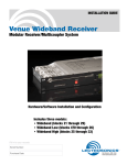
1
CRESCENT HEART SOFTWARE R4300 PROBING SUPPORT FOR USE WITH PA1-H16 PROBE ADAPTERS FOR PROBING MIPS R4300 PROCESSORS USING TEKTRONIX LOGIC ANALYZERS Produced by Crescent Heart Software, Portland Oregon, USA Telephone (503)232-2232; Facsimile (503)232-2255; E-mail [email protected]; Internet http://www.c-h-s.com Crescent Heart Software assumes no liability for errors, or for any incidental, consequential, indirect or special damages, including, without limitation, loss of use, loss or alteration of data, delays, or lost profits or savings, arising from the use of this document or any product which it accompanies. Copyright © Crescent Heart Software 1998. All rights reserved. Licensed software products are owned by Crescent Heart Software or its suppliers and are protected by United States copyright laws and international treaty provisions. This manual revision supersedes all previously published material. Specifications change privileges reserved. No part of this publication may be reproduced, stored in a retrieval system, or transmitted, in any form or by any means, mechanical, photocopying, recording or otherwise, without the prior written permission of Crescent Heart Software. TEKTRONIX is a registered trademark of Tektronix, Inc. All other company and product names are trademarks of their respective companies. Printed in the United States of America. Manual part number: MAN-R4300-PS Manual revision number 1.01 - October, 1998 Please register purchase of this software product upon receipt by requesting a registration form and returning the filled-out form back to us. Registration enables us to provide you with top flight technical support and to keep you informed of product updates and new products. Obtain a registration form by sending e-mail with "R4300-PS Registration" as the subject to [email protected]. Please communicate suggestions for product and documentation improvements to [email protected]. TABLE OF CONTENTS Section 1: Introduction 1.1 Connection To System Under Test . . . . . . . . . . . . . . . . . . . . . . . . . . . . . . . . . . . . . . . . . . . . . . . . . . . . . . . . 1.2 Software Versions . . . . . . . . . . . . . . . . . . . . . . . . . . . . . . . . . . . . . . . . . . . . . . . . . . . . . . . . . . . . . . . . . . . . . . 1.3 Installing Disassembler And Support Software . . . . . . . . . . . . . . . . . . . . . . . . . . . . . . . . . . . . . . . . . . . . . . 1.3.1 TLA7xx Installation . . . . . . . . . . . . . . . . . . . . . . . . . . . . . . . . . . . . . . . . . . . . . . . . . . . . . . . . . . . . . . 1.3.2 DAS9200/TLA5xx Installation . . . . . . . . . . . . . . . . . . . . . . . . . . . . . . . . . . . . . . . . . . . . . . . . . . . . . 1.4 Demonstration Acquisition Files . . . . . . . . . . . . . . . . . . . . . . . . . . . . . . . . . . . . . . . . . . . . . . . . . . . . . . . . . . 1.4.1 TLA7xx . . . . . . . . . . . . . . . . . . . . . . . . . . . . . . . . . . . . . . . . . . . . . . . . . . . . . . . . . . . . . . . . . . . . . . . . 1.4.2 DAS9200/TLA5xx . . . . . . . . . . . . . . . . . . . . . . . . . . . . . . . . . . . . . . . . . . . . . . . . . . . . . . . . . . . . . . . 1.5 LA-Offline And LA-Browser Tools . . . . . . . . . . . . . . . . . . . . . . . . . . . . . . . . . . . . . . . . . . . . . . . . . . . . . . . . 1.6 About This Manual . . . . . . . . . . . . . . . . . . . . . . . . . . . . . . . . . . . . . . . . . . . . . . . . . . . . . . . . . . . . . . . . . . . . . 1-1 1-1 1-1 1-1 1-2 1-2 1-2 1-2 1-3 1-3 Section 2: Setting Up The Hardware 2.1 Probing Connection Issues . . . . . . . . . . . . . . . . . . . . . . . . . . . . . . . . . . . . . . . . . . . . . . . . . . . . . . . . . . . . . . . 2.2 Configuring The Probe Adapter . . . . . . . . . . . . . . . . . . . . . . . . . . . . . . . . . . . . . . . . . . . . . . . . . . . . . . . . . . 2.2.1 J9 . . . . . . . . . . . . . . . . . . . . . . . . . . . . . . . . . . . . . . . . . . . . . . . . . . . . . . . . . . . . . . . . . . . . . . . . . . . . . 2.2.2 J10 . . . . . . . . . . . . . . . . . . . . . . . . . . . . . . . . . . . . . . . . . . . . . . . . . . . . . . . . . . . . . . . . . . . . . . . . . . . . 2.2.3 J11 . . . . . . . . . . . . . . . . . . . . . . . . . . . . . . . . . . . . . . . . . . . . . . . . . . . . . . . . . . . . . . . . . . . . . . . . . . . . 2.2.4 J12 . . . . . . . . . . . . . . . . . . . . . . . . . . . . . . . . . . . . . . . . . . . . . . . . . . . . . . . . . . . . . . . . . . . . . . . . . . . . 2.2.5 J13 . . . . . . . . . . . . . . . . . . . . . . . . . . . . . . . . . . . . . . . . . . . . . . . . . . . . . . . . . . . . . . . . . . . . . . . . . . . . 2.2.6 J14 . . . . . . . . . . . . . . . . . . . . . . . . . . . . . . . . . . . . . . . . . . . . . . . . . . . . . . . . . . . . . . . . . . . . . . . . . . . . 2-1 2-2 2-3 2-4 2-5 2-5 2-5 2-5 Section 3: Configuring The Acquisition Module 3.1 Loading Support Software . . . . . . . . . . . . . . . . . . . . . . . . . . . . . . . . . . . . . . . . . . . . . . . . . . . . . . . . . . . . . . . 3-1 3.1.1 TLA7xx . . . . . . . . . . . . . . . . . . . . . . . . . . . . . . . . . . . . . . . . . . . . . . . . . . . . . . . . . . . . . . . . . . . . . . . . 3-1 3.1.2 DAS9200/TLA5xx . . . . . . . . . . . . . . . . . . . . . . . . . . . . . . . . . . . . . . . . . . . . . . . . . . . . . . . . . . . . . . . 3-1 3.2 Channel Groupings . . . . . . . . . . . . . . . . . . . . . . . . . . . . . . . . . . . . . . . . . . . . . . . . . . . . . . . . . . . . . . . . . . . . . 3-3 3.3 Clocking Choices . . . . . . . . . . . . . . . . . . . . . . . . . . . . . . . . . . . . . . . . . . . . . . . . . . . . . . . . . . . . . . . . . . . . . . . 3-3 3.3.1 Clocking Delay . . . . . . . . . . . . . . . . . . . . . . . . . . . . . . . . . . . . . . . . . . . . . . . . . . . . . . . . . . . . . . . . . . 3-3 3.3.1.1 Setting The Clocking Delay . . . . . . . . . . . . . . . . . . . . . . . . . . . . . . . . . . . . . . . . . . . . . . . . 3-4 3.3.2 Canceled Transactions Field . . . . . . . . . . . . . . . . . . . . . . . . . . . . . . . . . . . . . . . . . . . . . . . . . . . . . . . 3-5 3.3.3 Nonissue Request Cycles Field . . . . . . . . . . . . . . . . . . . . . . . . . . . . . . . . . . . . . . . . . . . . . . . . . . . . . 3-5 3.3.4 Data Wait And Idle Cycles Field . . . . . . . . . . . . . . . . . . . . . . . . . . . . . . . . . . . . . . . . . . . . . . . . . . . . 3-6 3.3.5 Acquisition Field . . . . . . . . . . . . . . . . . . . . . . . . . . . . . . . . . . . . . . . . . . . . . . . . . . . . . . . . . . . . . . . . . 3-7 3.4 Symbols And Symbol Tables . . . . . . . . . . . . . . . . . . . . . . . . . . . . . . . . . . . . . . . . . . . . . . . . . . . . . . . . . . . . . 3-7 3.5 Triggering . . . . . . . . . . . . . . . . . . . . . . . . . . . . . . . . . . . . . . . . . . . . . . . . . . . . . . . . . . . . . . . . . . . . . . . . . . . . 3-12 Section 4: Disassembly Display Of Data 4.1 Acquiring Data . . . . . . . . . . . . . . . . . . . . . . . . . . . . . . . . . . . . . . . . . . . . . . . . . . . . . . . . . . . . . . . . . . . . . . . . 4.2 Fundamental Disassembly Issues . . . . . . . . . . . . . . . . . . . . . . . . . . . . . . . . . . . . . . . . . . . . . . . . . . . . . . . . . 4.2.1 Processor Bus Addresses . . . . . . . . . . . . . . . . . . . . . . . . . . . . . . . . . . . . . . . . . . . . . . . . . . . . . . . . . . 4.2.1.1 PC-With-Displacement Calculations . . . . . . . . . . . . . . . . . . . . . . . . . . . . . . . . . . . . . . . . . 4.2.1.2 SysAddr Group Symbol Table . . . . . . . . . . . . . . . . . . . . . . . . . . . . . . . . . . . . . . . . . . . . . . 4.2.2 Memory Access Caching . . . . . . . . . . . . . . . . . . . . . . . . . . . . . . . . . . . . . . . . . . . . . . . . . . . . . . . . . . 4.2.3 Subblock Data Transfer Order . . . . . . . . . . . . . . . . . . . . . . . . . . . . . . . . . . . . . . . . . . . . . . . . . . . . . . 4.2.4 Tracing Control Flow . . . . . . . . . . . . . . . . . . . . . . . . . . . . . . . . . . . . . . . . . . . . . . . . . . . . . . . . . . . . . 4.2.5 Reduced Power Mode Cycles . . . . . . . . . . . . . . . . . . . . . . . . . . . . . . . . . . . . . . . . . . . . . . . . . . . . . . 4.3 Understanding The Disassembly Display . . . . . . . . . . . . . . . . . . . . . . . . . . . . . . . . . . . . . . . . . . . . . . . . . . . R4300 Probing Support Manual 4-1 4-1 4-1 4-2 4-2 4-3 4-3 4-3 4-3 4-4 i Table Of Contents 4.4 Disassembly Format Definition Overlay . . . . . . . . . . . . . . . . . . . . . . . . . . . . . . . . . . . . . . . . . . . . . . . . . . . . 4-5 4.4.1 Display Mode Field . . . . . . . . . . . . . . . . . . . . . . . . . . . . . . . . . . . . . . . . . . . . . . . . . . . . . . . . . . . . . . 4-5 4.4.1.1 Hardware Display Format . . . . . . . . . . . . . . . . . . . . . . . . . . . . . . . . . . . . . . . . . . . . . . . . . 4-6 4.4.1.2 Software Display Format . . . . . . . . . . . . . . . . . . . . . . . . . . . . . . . . . . . . . . . . . . . . . . . . . . 4-7 4.4.1.3 Control Flow Display Format . . . . . . . . . . . . . . . . . . . . . . . . . . . . . . . . . . . . . . . . . . . . . . . 4-8 4.4.1.4 Subroutine Display Format . . . . . . . . . . . . . . . . . . . . . . . . . . . . . . . . . . . . . . . . . . . . . . . . 4-8 4.4.2 Disassemble Across Gaps Field . . . . . . . . . . . . . . . . . . . . . . . . . . . . . . . . . . . . . . . . . . . . . . . . . . . . . 4-9 4.4.3 H/W Cycles Displayed Field . . . . . . . . . . . . . . . . . . . . . . . . . . . . . . . . . . . . . . . . . . . . . . . . . . . . . . . 4-9 4.4.4 RegNames, ByteOrder Field . . . . . . . . . . . . . . . . . . . . . . . . . . . . . . . . . . . . . . . . . . . . . . . . . . . . . . 4-10 4.4.5 Exceptions Field . . . . . . . . . . . . . . . . . . . . . . . . . . . . . . . . . . . . . . . . . . . . . . . . . . . . . . . . . . . . . . . . 4-12 4.4.6 Uncached Area Begin Field . . . . . . . . . . . . . . . . . . . . . . . . . . . . . . . . . . . . . . . . . . . . . . . . . . . . . . . 4-12 4.4.7 Uncached Area Size Field . . . . . . . . . . . . . . . . . . . . . . . . . . . . . . . . . . . . . . . . . . . . . . . . . . . . . . . . 4-12 4.5 Marking Samples . . . . . . . . . . . . . . . . . . . . . . . . . . . . . . . . . . . . . . . . . . . . . . . . . . . . . . . . . . . . . . . . . . . . . . 4-12 4.6 Alternative Data Displays . . . . . . . . . . . . . . . . . . . . . . . . . . . . . . . . . . . . . . . . . . . . . . . . . . . . . . . . . . . . . . . 4-14 4.6.1 State Display . . . . . . . . . . . . . . . . . . . . . . . . . . . . . . . . . . . . . . . . . . . . . . . . . . . . . . . . . . . . . . . . . . . 4-14 4.6.2 Timing Display . . . . . . . . . . . . . . . . . . . . . . . . . . . . . . . . . . . . . . . . . . . . . . . . . . . . . . . . . . . . . . . . . 4-14 4.6.2.1 Delayed Signals . . . . . . . . . . . . . . . . . . . . . . . . . . . . . . . . . . . . . . . . . . . . . . . . . . . . . . . . . 4-14 Section 5: Acquisition Clocking Choices 5.1 Custom Clocking . . . . . . . . . . . . . . . . . . . . . . . . . . . . . . . . . . . . . . . . . . . . . . . . . . . . . . . . . . . . . . . . . . . . . . . 5-1 5.2 External Clocking . . . . . . . . . . . . . . . . . . . . . . . . . . . . . . . . . . . . . . . . . . . . . . . . . . . . . . . . . . . . . . . . . . . . . . 5-1 5.3 Internal Clocking . . . . . . . . . . . . . . . . . . . . . . . . . . . . . . . . . . . . . . . . . . . . . . . . . . . . . . . . . . . . . . . . . . . . . . . 5-2 ii R4300 Probing Support Manual Table Of Contents APPENDICES Appendix A: Processor Characteristics A.1 R4300 . . . . . . . . . . . . . . . . . . . . . . . . . . . . . . . . . . . . . . . . . . . . . . . . . . . . . . . . . . . . . . . . . . . . . . . . . . . . . . . A-1 Appendix B: SMT-To-PGA Adapter B.1 Notes . . . . . . . . . . . . . . . . . . . . . . . . . . . . . . . . . . . . . . . . . . . . . . . . . . . . . . . . . . . . . . . . . . . . . . . . . . . . . . . B-1 Appendix C: PGA-Socket Signal List Appendix D: Acquisition Modules’ Signal Lists Appendix E: Channel Assignments E.1 SysAddr Group . . . . . . . . . . . . . . . . . . . . . . . . . . . . . . . . . . . . . . . . . . . . . . . . . . . . . . . . . . . . . . . . . . . . . . . E.2 Control Group . . . . . . . . . . . . . . . . . . . . . . . . . . . . . . . . . . . . . . . . . . . . . . . . . . . . . . . . . . . . . . . . . . . . . . . . E.3 A Group . . . . . . . . . . . . . . . . . . . . . . . . . . . . . . . . . . . . . . . . . . . . . . . . . . . . . . . . . . . . . . . . . . . . . . . . . . . . . E.4 Intr Group . . . . . . . . . . . . . . . . . . . . . . . . . . . . . . . . . . . . . . . . . . . . . . . . . . . . . . . . . . . . . . . . . . . . . . . . . . . E.5 Misc Group . . . . . . . . . . . . . . . . . . . . . . . . . . . . . . . . . . . . . . . . . . . . . . . . . . . . . . . . . . . . . . . . . . . . . . . . . . E.6 DivMode Group . . . . . . . . . . . . . . . . . . . . . . . . . . . . . . . . . . . . . . . . . . . . . . . . . . . . . . . . . . . . . . . . . . . . . . E.7 Clks Group . . . . . . . . . . . . . . . . . . . . . . . . . . . . . . . . . . . . . . . . . . . . . . . . . . . . . . . . . . . . . . . . . . . . . . . . . . E.8 JTAG Group . . . . . . . . . . . . . . . . . . . . . . . . . . . . . . . . . . . . . . . . . . . . . . . . . . . . . . . . . . . . . . . . . . . . . . . . . E.9 Unused Group . . . . . . . . . . . . . . . . . . . . . . . . . . . . . . . . . . . . . . . . . . . . . . . . . . . . . . . . . . . . . . . . . . . . . . . E.10 UnusedC3 Group . . . . . . . . . . . . . . . . . . . . . . . . . . . . . . . . . . . . . . . . . . . . . . . . . . . . . . . . . . . . . . . . . . . . E.11 UnusedC2 Group . . . . . . . . . . . . . . . . . . . . . . . . . . . . . . . . . . . . . . . . . . . . . . . . . . . . . . . . . . . . . . . . . . . . E.12 UnusedC0 Group . . . . . . . . . . . . . . . . . . . . . . . . . . . . . . . . . . . . . . . . . . . . . . . . . . . . . . . . . . . . . . . . . . . . E.13 UnusedD3 Group . . . . . . . . . . . . . . . . . . . . . . . . . . . . . . . . . . . . . . . . . . . . . . . . . . . . . . . . . . . . . . . . . . . . E.14 UnusedD2 Group . . . . . . . . . . . . . . . . . . . . . . . . . . . . . . . . . . . . . . . . . . . . . . . . . . . . . . . . . . . . . . . . . . . . E.15 UnusedD1 Group . . . . . . . . . . . . . . . . . . . . . . . . . . . . . . . . . . . . . . . . . . . . . . . . . . . . . . . . . . . . . . . . . . . . E.16 UnusedD0 Group . . . . . . . . . . . . . . . . . . . . . . . . . . . . . . . . . . . . . . . . . . . . . . . . . . . . . . . . . . . . . . . . . . . . E.17 DAS9200/TLA5xx Clock Probe Connections . . . . . . . . . . . . . . . . . . . . . . . . . . . . . . . . . . . . . . . . . . . . . . E-1 E-3 E-3 E-4 E-4 E-4 E-5 E-5 E-5 E-6 E-6 E-6 E-7 E-7 E-8 E-8 E-8 Appendix F: Support For LA-Offline And LA-Browser Tools F.1 R4300A Support Application For LA-Offline For Windows . . . . . . . . . . . . . . . . . . . . . . . . . . . . . . . . . . . F.2 R4300A Support Application For LA-Offline For The Sun . . . . . . . . . . . . . . . . . . . . . . . . . . . . . . . . . . . . F.2.1 Installation When Using SunOS 4.1.X (Solaris 1.1) . . . . . . . . . . . . . . . . . . . . . . . . . . . . . . . . . . . . F.2.2 Installation When Using SunOS 5.3 (Solaris 2.3) . . . . . . . . . . . . . . . . . . . . . . . . . . . . . . . . . . . . . . F.2.3 Uninstallation . . . . . . . . . . . . . . . . . . . . . . . . . . . . . . . . . . . . . . . . . . . . . . . . . . . . . . . . . . . . . . . . . . F.3 Notes Regarding Use Of LA-Offline . . . . . . . . . . . . . . . . . . . . . . . . . . . . . . . . . . . . . . . . . . . . . . . . . . . . . . F.4 Notes Regarding Use Of LA-Browser . . . . . . . . . . . . . . . . . . . . . . . . . . . . . . . . . . . . . . . . . . . . . . . . . . . . . F-1 F-1 F-1 F-2 F-2 F-3 F-3 Appendix G: Warranty And Service Appendix H: History Of Revisions H.1 Manual Revision History . . . . . . . . . . . . . . . . . . . . . . . . . . . . . . . . . . . . . . . . . . . . . . . . . . . . . . . . . . . . . . . H-1 H.2 Software Revision History . . . . . . . . . . . . . . . . . . . . . . . . . . . . . . . . . . . . . . . . . . . . . . . . . . . . . . . . . . . . . . H-1 R4300 Probing Support Manual iii Table Of Contents LIST OF FIGURES Figure 2.1: Representative SMT-To-PGA Adapter Dimensions . . . . . . . . . . . . . . . . . . . . . . . . . . . . . . . . . . . 2-2 Figure 2.2: Probe Adapter Component Location . . . . . . . . . . . . . . . . . . . . . . . . . . . . . . . . . . . . . . . . . . . . . . . . 2-3 Figure 3.1: LA Module Setup Window . . . . . . . . . . . . . . . . . . . . . . . . . . . . . . . . . . . . . . . . . . . . . . . . . . . . . . . 3-2 Figure 3.2: LA Module Setup Window Custom Clocking options . . . . . . . . . . . . . . . . . . . . . . . . . . . . . . . . . 3-4 Figure 4.1: Figure 4.2: Figure 4.3: Figure 4.4: Figure 4.5: Example Disassembly Display . . . . . . . . . . . . . . . . . . . . . . . . . . . . . . . . . . . . . . . . . . . . . . . . . . . . . 4-2 Disassembly Properties Page . . . . . . . . . . . . . . . . . . . . . . . . . . . . . . . . . . . . . . . . . . . . . . . . . . . . . . 4-6 Example Of Hardware Display Format . . . . . . . . . . . . . . . . . . . . . . . . . . . . . . . . . . . . . . . . . . . . . 4-7 Example Of Special Cycles Hardware Display . . . . . . . . . . . . . . . . . . . . . . . . . . . . . . . . . . . . . . 4-10 Timing Display Of An Acquire-All-Cycles Custom Clocking Acquisition . . . . . . . . . . . . . . . . 4-15 Figure 5.1: Example Timing Display Of An Internal Clocking Acquisition . . . . . . . . . . . . . . . . . . . . . . . . . . 5-3 LIST OF TABLES Table 2.1: Probe Adapter Probe Connections . . . . . . . . . . . . . . . . . . . . . . . . . . . . . . . . . . . . . . . . . . . . . . . . . . 2-4 Table 3.1: Control Group Symbol Table (R4300A_Ctrl) . . . . . . . . . . . . . . . . . . . . . . . . . . . . . . . . . . . . . . . . . . 3-8 Table 3.2: Intr Group Symbol Table (R4300A_Intr) . . . . . . . . . . . . . . . . . . . . . . . . . . . . . . . . . . . . . . . . . . . . 3-10 Table 4.1: Processor General Purpose Register Names . . . . . . . . . . . . . . . . . . . . . . . . . . . . . . . . . . . . . . . . . . 4-11 Table 4.2: Exception Vector Labeling . . . . . . . . . . . . . . . . . . . . . . . . . . . . . . . . . . . . . . . . . . . . . . . . . . . . . . . . 4-13 Table B.1: R4300 Adapter SMT to PGA-Socket Signal Connection List . . . . . . . . . . . . . . . . . . . . . . . . . . . . B-2 Table B.2: R4300 Adapter PGA-Socket to SMT Signal Connection List . . . . . . . . . . . . . . . . . . . . . . . . . . . . B-3 Table D.1: DAS9200/TLA5xx Acquisition Module Signal List . . . . . . . . . . . . . . . . . . . . . . . . . . . . . . . . . . . D-2 Table D.2: TLA7xx Acquisition Module Signal List . . . . . . . . . . . . . . . . . . . . . . . . . . . . . . . . . . . . . . . . . . . . D-3 Table E.1: SysAddr Group Channel Assignments . . . . . . . . . . . . . . . . . . . . . . . . . . . . . . . . . . . . . . . . . . . . . Table E.2: Control Group Channel Assignments . . . . . . . . . . . . . . . . . . . . . . . . . . . . . . . . . . . . . . . . . . . . . . Table E.3: A Group Channel Assignments . . . . . . . . . . . . . . . . . . . . . . . . . . . . . . . . . . . . . . . . . . . . . . . . . . . Table E.4: Intr Group Channel Assignments . . . . . . . . . . . . . . . . . . . . . . . . . . . . . . . . . . . . . . . . . . . . . . . . . . Table E.5: Misc Group Channel Assignments . . . . . . . . . . . . . . . . . . . . . . . . . . . . . . . . . . . . . . . . . . . . . . . . . Table E.6: DivMode Group Channel Assignments . . . . . . . . . . . . . . . . . . . . . . . . . . . . . . . . . . . . . . . . . . . . Table E.7: Clks Group Channel Assignments . . . . . . . . . . . . . . . . . . . . . . . . . . . . . . . . . . . . . . . . . . . . . . . . . Table E.8: JTAG Group Channel Assignments . . . . . . . . . . . . . . . . . . . . . . . . . . . . . . . . . . . . . . . . . . . . . . . . Table E.9: Unused Group Channel Assignments . . . . . . . . . . . . . . . . . . . . . . . . . . . . . . . . . . . . . . . . . . . . . . Table E.10: UnusedC3 Group Channel Assignments . . . . . . . . . . . . . . . . . . . . . . . . . . . . . . . . . . . . . . . . . . . Table E.11: UnusedC2 Group Channel Assignments . . . . . . . . . . . . . . . . . . . . . . . . . . . . . . . . . . . . . . . . . . . Table E.12: UnusedC0 Group Channel Assignments . . . . . . . . . . . . . . . . . . . . . . . . . . . . . . . . . . . . . . . . . . . Table E.13: UnusedD3 Group Channel Assignments . . . . . . . . . . . . . . . . . . . . . . . . . . . . . . . . . . . . . . . . . . . Table E.14: UnusedD2 Group Channel Assignments . . . . . . . . . . . . . . . . . . . . . . . . . . . . . . . . . . . . . . . . . . . Table E.15: UnusedD1 Group Channel Assignments . . . . . . . . . . . . . . . . . . . . . . . . . . . . . . . . . . . . . . . . . . . Table E.16: UnusedD0 Group Channel Assignments . . . . . . . . . . . . . . . . . . . . . . . . . . . . . . . . . . . . . . . . . . . Table E.17: DAS9200/TLA5xx Clock Probe Connections . . . . . . . . . . . . . . . . . . . . . . . . . . . . . . . . . . . . . . . iv E-2 E-3 E-3 E-4 E-4 E-4 E-5 E-5 E-5 E-6 E-6 E-6 E-7 E-7 E-8 E-8 E-8 R4300 Probing Support Manual 1. INTRODUCTION This manual describes R4300 probing support for probing SMT-package MIPS R4300 processors using Tektronix logic analyzers. 1.1 CONNECTION TO SYSTEM UNDER TEST Connection to the R4300 system under test may be accomplished through the use of a PA1-H16 probe adapter and an R4300 SMT adapter. The probe adapter accepts connection of standard logic analyzer probes. Alternatively, direct connection to the system under test can be accomplished via through-hole headers or through-hole/SMT Mictor ( AMP) connectors designed into the system under test to which standard or high-density logic analyzer probes can mate. 1.2 SOFTWARE VERSIONS Two versions of R4300 software support are available: w the CHS204 R4300A disassembler provides support for use with DAS9200 or TLA5xx logic analyzers and requires a single 96-channel acquisition module; w the CHS304 R4300A disassembler provides support for use with TLA7xx logic analyzers and requires a single acquisition module of at least 102 channels. Note that probing an R4300 processor using the PA1-H16 probe adapter and a DAS9200 or TLA5xx analyzer may be problematic due to the complex clock timing utilized by the processor. Such probing may require use instead of an R4XXX-R type probe adapter and appropriate software support, which have been designed to provide the DAS9200 or TLA5xx with the means to deal with complex clock timing. This manual is oriented toward presenting the features and functions of the software and hardware in the context of use with a TLA7xx logic analyzer. Any significant differences which may be encountered when using a DAS9200 or TLA5xx logic analyzer are noted. Note that the screen shots presented herein are TLA7xx displays. 1.3 INSTALLING DISASSEMBLER AND SUPPORT SOFTWARE 1.3.1 TLA7xx Installation Install the new disassembly support software on the TLA7xx logic analyzer in the same manner that other software is installed on a Windows95 system: insert the disassembly support disk in the floppy disk drive (disk label facing to the front for a portable unit; disk label facing to the right for a rack-mount unit); click on the Windows95 Start button; choose Settings...; choose Control Panel; double-click on Add/Remove Programs; click on Install... under the Install/Uninstall tab; then follow the on-screen directions. Prior to installing the disassembly support software, remove any extant version of that same software (e.g., any earlier version). When in Add/Remove Programs, review the list of programs already present in the system. If a version of the support software already exists, select it and click on Remove. Once removal is complete, continue on to install the new software then as instructed in the preceding paragraph. R4300 Probing Support Manual 1-1 Introduction 1.3.2 DAS9200/TLA5xx Installation The software is compatible with any DAS9200/TLA5xx System Software Release 3, Version 1.3 or later and an X window display on either a workstation (X terminal) or an X11/R4-compatible display. Attempted installation on an incompatible system or terminal using System Software Release 3, V1.1 or later results in no installation and the display of an error message. Installation on an incompatible system or terminal using System Software Release 3, V1.0 or earlier results in an apparently successful installation, however the software will not operate properly. Install the new application software on the logic analyzer as follows: 1. Insert the disk with the software into the floppy disk drive of the logic analyzer. 2. Choose Disk Services under Utilities on the main menu if not previously selected. 3. Select Install Application in the Operation field of the Disk Services menu. 4. Press F8: EXECUTE OPERATION and follow the on-screen prompts. At the completion of the software installation, the display will indicate success or failure. If a problem occurs, applications or files may have to be removed from the hard drive of the analyzer and the software installation attempted again. 1.4 DEMONSTRATION ACQUISITION FILES 1.4.1 TLA7xx Demonstration acquisitions in the form of previously-saved module setup files are provided to show how the disassembler displays instruction mnemonics and processor bus cycle types. The acquisitions also afford a means of becoming familiar with the operation and control of the disassembler prior to probing the system under test. Three demonstration acquisition files are provided: w File demo.tla is a synchronous (Custom clocking) acquisition of an R4300 system starting up (from the deassertion of ResetB) with the usual cycles of interest (e.g., memory request and memory data cycles) captured; w File demoAllCycles.tla is similar to demo.tla except that all bus cycles have been captured; w File timing.tla is an asynchronous (Internal clocking) acquisition of the R4300 system starting up (from the deassertion of ResetB). View a demonstration acquisition by selecting Load System from the File menu, and then select the setup file (.tla file extension) to be loaded. The demonstration files should be found in the C:\Program Files\TLA 700\Supports\R4300A folder. Refer to Section 4.4, Disassembly Format Definition Overlay, and related sections for information on controlling the disassembler and its display 1.4.2 DAS9200/TLA 5xx A single reference memory, R4300A_Demo, is provided. 1-2 R4300 Probing Support Manual Introduction 1.5 LA-OFFLINE AND LA-BROWSER TOOLS R4300A support for the Tektronix LA-Offline data analysis software tool for the PC and for the Sun may also be provided along with the basic disassembly support. Refer to Appendix F, Support For LA-Offline and LA-Browser Tools, for information on installation of R4300A support for use with LA-Offline, as well as information concerning the use of R4300A support with LA-Offline and LA-Browser. 1.6 ABOUT THIS MANUAL This manual is organized as follows: Section 1: Introduction - Presents information on installing disassembler software; viewing the demonstration acquisition files; and manual organization. Section 2: Setting Up The Hardware - Discusses probe adapter and SMT adapter issues, including configuring the probe adapter. Section 3: Configuring The Acquisition Module - Information is provided on setting up the acquisition module in preparation for data acquisition and disassembly display. Section 4: Disassembly Display Of Data - Discusses how to acquire data and view it, principally using the disassembly display. Section 5: Acquisition Clocking Choices - A discussion of the acquisition clocking choices available and their uses. Appendix A: Processor Characteristics Appendix B: SMT-To-PGA Adapter Appendix C: PGA-Socket Signal List Appendix D: Acquisition Modules’ Signal Lists Appendix E: Channel Assignments Appendix F: Support For LA-Offline and LA-Browser Tools Appendix G: Warranty And Service Appendix H: History Of Revisions R4300 Probing Support Manual 1-3 Introduction This page has been left blank intentionally. 1-4 R4300 Probing Support Manual 2. SETTING UP THE HARDWARE Connection to the R4300 system under test (SUT) may be accomplished through the use of a PA1-H16 probe adapter and an R4300 SMT adapter. The probe adapter accepts connection of standard logic analyzer probes. Alternatively, direct connection to the system under test can be accomplished via through-hole headers or through-hole/SMT Mictor ( AMP) connectors designed into the system under test to which standard or high-density logic analyzer probes can mate. The presentation here is oriented toward use of the PA1-H16 probe adapter. Refer to Appendix E, Channel Assignments, for signal connection information required to implement direct connection of the logic analyzer to the system under test. 2.1 PROBING CONNECTION ISSUES An R4300 SMT-to-PGA adapter is used along with the PA1-H16 probe adapter to enable probing of the SMT-package R4300 processor. The R4300 SMT adapter is a clip-on adapter. The unit clips on top of the SMT-package processor present on the SUT motherboard. The SMT adapter provides a PGA socket into which the probe adapter plugs. Figure 2.1 shows drawings of a representative clip-on SMT adapter. The R4300 SMT adapter has similar dimensions, with only dimensions “B” and “C” being fundamentally different (although even so the C-B difference shown in the figure is approximately the same). It is recommended that the design of the SUT motherboard accommodate the use of the SMT adapter by providing a set of four mounting holes, corresponding to the four holes present as shown on the SMT adapter. This allows the SMT adapter to be mechanically secured to the SUT motherboard through the use of spacers, machine bolts or screws, washers and nuts. One of the corners of the SMT adapter's upper printed circuit board (PCB) is cut (chamfered); that corner of the SMT clip corresponds to SMT pin 1 of the processor. Usually, the same (corresponding) corners of both the upper and lower PCBs of the SMT adapter will be chamfered. On some units non-corresponding corners may be chamfered; for such units it is the chamfered corner of the lower PCB that corresponds to SMT pin 1. If using an SMT adapter which is not being secured to the SUT motherboard, do not attempt to clip the SMT adapter onto the processor until the probe adapter has been configured (as discussed later), the logic analyzer probes have been attached to the probe adapter, and the probe adapter and SMT adapter have been mated together. Clipping onto the processor chip should be the very last step. Special care should be exercised when clipping the SMT adapter onto (and off from) the processor chip. Care should be taken to insure that the clip is oriented properly (pin 1 orientation, as discussed above), and also that the clip is not being placed at an angle onto the processor. The processor leads at the extreme ends of each of the four sides of the chip are susceptible to being bent or moved sideways (thereby possibly contacting a neighboring lead) when the alignment of the SMT adapter is improper. Note that while use of a clip-on SMT adapter to probe more than one chip is possible, such multi-chip probing tends to shorten the adapter’s reliable probing lifetime; it is recommended that a given adapter be dedicated if possible for use in probing just one particular processor. Also, by reducing the number of times an adapter is clipped onto and removed from a chip, the longer its reliable probing lifetime can be expected to be. Verify that no power-to-ground short circuit exists on the SUT as the result of attaching the adapter to the motherboard before applying SUT power. R4300 Probing Support Manual 2-1 Setting Up The Hardware Figure 2.1 - Representative SMT-To-PGA Adapter Dimensions !WARNING! Vcc (a direct low-impedance connection to SUT power) exists on various pins of the PGA socket of the SMT adapter and the probe adapter. Power pins are exposed when a clip-on SMT-to-PGA adapter is used to probe an SMT-package processor. For further information concerning the SMT adapter, refer to Appendix B, SMT-To-PGA Adapter. 2.2 CONFIGURING THE PROBE ADAPTER Figure 2.2 shows a drawing of the PA1-H16 probe adapter as viewed from the top. The probe adapter has no active components, and the only passive components present are capacitors decoupling the SUT Vcc power (+5 Volts or +3.3 Volts) to ground (a total of approximately 68.12 uF). The dimensions of the probe adapter are 3.7” (9,4 cm) by 3.7” (9,4 cm). In the drawing PGA socket pin location A1 (shown as square-shaped in the drawing) is toward the lower left corner; pin location A1 is positioned 1.0” (2,5 cm) from both edges of the probe adapter PCB. The pin numbering for the pins of the PGA socket is as follows. Each pin is identified by a column identifier (A, B, C, D, E, F, G, H, J, K, L, M, N, P, R, T, U, V) followed by a row identifier (1 through 18). Pin location A1 is at the lower left corner of the PGA socket; pin A18 is in the upper left corner; pin V18 is in the upper right corner; pin V1 is in the lower right corner. 2-2 R4300 Probing Support Manual Setting Up The Hardware Figure 2.2 - Probe Adapter Component Location Each of the 2x19 headers shown in the drawing, labeled J1 through J8, allow for connection of three logic analyzer probes: two 8-channel probes and a single clock or qualifier probe. The probes plug onto the headers of the PCB such that the signal connection(s) of the probe are placed closer to the PGA socket and the ground connection(s) of the probe are placed away from the PGA socket. Insure that all probes are oriented properly on the headers to avoid shorting the signals of the processor and SUT to ground. Table 2.1 lists which probe adapter connectors receive which of the various logic analyzer probes, based on the type of logic analyzer being used. Note that for the 8-channel probes channel 7 is located on the probe adapter PCB as the left- (or bottom-) most probe of the probe group; channel 0 is the right- (or top-) most probe. Each of the 1x3 headers shown in the drawing, labeled J9 through J14, must be configured properly based on the type of logic analyzer being used, as discussed below. Note that it will usually be simpler to first configure the probe adapter jumpers, and then connect the logic analyzer probes. 2.2.1 J9 The jumper position on this header determines which signal is routed to the top J1 connector on the probe adapter PCB. With the jumper in its up position, the connector receives the signal from probe adapter PGA socket pin J17; with the jumper in its down position, the connector receives the signal from the probe adapter PGA socket pin U4. When using DAS9200 or TLA5xx logic analyzers no probe is connected to the connector; when using TLA7xx analyzers, the probe that is connected is unused (it is “parked” there). Therefore, the J9 jumper position doesn’t matter, and the jumper is usually simply removed. Summary: J9 is removed. R4300 Probing Support Manual 2-3 Setting Up The Hardware Connector - Position DAS9200 / TLA5xx TLA7xx J1 - Top no connection Clk:0 J1 - Middle A3 A3 J1 - Bottom A2 A2 J2 - Top Clk:1 Clk:1 J2 - Middle A1 A1 J2 - Bottom A0 A0 J3 - Left C2 C2 J3 - Middle D3 C3 J3 - Right no connection Clk:3 J4 - Left C1 C1 J4 - Middle C0 C0 J4 - Right Clk:0 Q1 J5 - Top Clk:2 Clk:2 J5 - Middle no connection no connection J5 - Bottom no connection no connection J6 - Top no connection no connection J6 - Middle no connection no connection J6 - Bottom no connection no connection J7 - Left D2 D2 J7 - Middle C3 D3 J7 - Right Clk:3 Q0 J8 - Left D0 D0 J8 - Middle D1 D1 J8 - Right no connection no connection Table 2.1 - Probe Adapter Probe Connections 2.2.2 J10 The jumper position on this header determines which signal is routed to the top J2 connector, where the Clk:1 logic analyzer probe connects. With the jumper in its up position, Clk:1 receives the signal from pin C17 of the probe adapter PGA socket, the TClock0 signal as provided by the R4300 SMT adapter; with the jumper in its down position, Clk:1 receives the signal from pin D16 of the probe adapter PGA socket (this signal is undefined by the R4300 SMT adapter). Summary: J10 is placed in its up position. 2-4 R4300 Probing Support Manual Setting Up The Hardware 2.2.3 J11 The jumper position on this header determines which signal is routed to the right J3 connector. With the jumper in its right position, the connector receives the EValidInB signal from the probe adapter PGA socket (PGA pin P2); with the jumper in its left position, the receives the signal from probe adapter PGA socket pin B4 (this signal is undefined by the R4300 SMT adapter). When using DAS9200 or TLA5xx logic analyzers no probe is connected to the connector; when using TLA7xx analyzers, the probe that is connected is unused (it is parked there). Therefore, the J11 jumper position doesn’t matter, and the jumper is usually simply removed. Summary: J11 is removed. 2.2.4 J12 The jumper position on this header determines which signal is routed to the D3:7 logic analyzer probe when using DAS9200 or TLA5xx logic analyzers, or to the C3:7 logic analyzer probe when using TLA7xx logic analyzers. With the jumper in its right position, the probe receives the PReqB signal from the probe adapter PGA socket (PGA pin T5); with the jumper in its left position, the probe receives the signal from probe adapter PGA socket pin M17 (this signal is undefined by the R4300 SMT adapter). When using DAS9200 or TLA5xx logic analyzers, D3:7 should have the PReqB signal, and therefore the jumper should be placed in its right position; when using TLA7xx logic analyzers, C3:7 is unused, and therefore the jumper should be removed. Summary: For DAS9200 or TLA5xx analyzers, J12 is usually placed in its right position; for TLA7xx analyzers, J12 is removed. 2.2.5 J13 The jumper position on this header determines which signal is routed to the C0:7 logic analyzer probe. With the jumper in its right position, the probe receives the EValidInB signal from the probe adapter PGA socket (PGA pin P2); with the jumper in its left position, the probe receives the ColdResetB signal from the probe adapter PGA socket (PGA pin T14). When using DAS9200 or TLA5xx logic analyzers, the jumper should be placed in its right position. When using a TLA7xx logic analyzer, the jumper should be placed in its left position. Summary: For DAS9200 or TLA5xx analyzers, J13 is usually placed in its right position; for TLA7xx analyzers, J13 is usually placed in its left position. 2.2.6 J14 The jumper position on this header determines which signal is routed to the top J6 connector. With the jumper in its up position, the connector receives the signal from pin T17 of the probe adapter PGA socket; with the jumper in its down position, the connector receives the signal from pin R16 of the probe adapter PGA socket. The R4300 SMT adapter defines neither of these signals. Summary: J14 is removed. R4300 Probing Support Manual 2-5 Setting Up The Hardware This page has been left blank intentionally. 2-6 R4300 Probing Support Manual 3. CONFIGURING THE ACQUISITION MODULE This section provides information on setting up the acquisition module in preparation for data acquisition and disassembly display. Information is provided on the following: w loading support software w channel groupings w clocking choices w symbols and symbol tables w triggering 3.1 LOADING SUPPORT SOFTWARE Assuming the software has already been installed on the analyzer (i.e., copied from floppy disk to the hard drive of the system; refer to Section 1.3, Installing Disassembler And Support Software), the software can then be loaded into the acquisition module. 3.1.1 TLA7xx In order to get ready to perform a disassembly acquisition the support software must be loaded into the acquisition module: select Load Support Package... from the File menu and select R4300A (found in the C:\Program Files\TLA700\Supports folder). Another way to get ready to perform a disassembly acquisition is to load a previously-saved system setup file: select Load System... from the File menu, and then select the setup file (.tla file extension) desired. For example, the demo.tla demonstration disassembly acquisition file supplied with the disassembly support can be loaded (found in the C:\Program Files\TLA700\Supports\R4300A folder). With the load performed, the LA module Setup window will show relevant acquisition-related information concerning: what channel groupings have been setup; the clocking mode; the memory depth; etc. Changes to these parameters can be made also via the LA module Setup window. Figure 3.1 shows the LA module Setup window. 3.1.2 DAS9200/TLA5xx If the logic analyzer has more than one 92A96 or 92C96 acquisition module in adjacent slots, the modules are automatically formed into a variable-width (multicard) module by system software at power on. In such a situation the modules must be reconfigured prior to loading the support software on the individual module of interest; this reconfiguration is done using the System Configuration menu. Refer to the discussion in the DAS System User Manual for details on reconfiguring variable-width (multicard) modules. R4300 Probing Support Manual 3-1 Configuring The Acquisition Module Figure 3.1 - LA Module Setup Window Do the following to load the software: 1. On the main menu select the 92A96 or 92C96 module of interest. 2. Choose Configuration under Setup on the main menu. 3. Select R4300A Support in the Software Support field. 4. Press F8: EXECUTE OPERATION. When the software is loaded, the Channel, Clock and Trigger setup menus are configured automatically to acquire data from the system under test. Changes made to the setup menus can be saved using Save/Restore under Utilities on the main menu and selecting Save Module Setup; use Restore Setup later to restore the saved acquisition module configuration. 3-2 R4300 Probing Support Manual Configuring The Acquisition Module 3.2 CHANNEL GROUPINGS The disassembler software automatically defines the channel groups for the signals of the processor. The channel groups defined include: SysAddr, Control, A, Intr, Misc, DivMode, Clks, JTAG, Unused, UnusedC3, UnusedC2, UnusedC0, UnusedD3, UnusedD2, UnusedD1 and UnusedD0. Refer to the LA module Setup window to view or change the channel assignments; also refer to the channel assignment tables in Appendix E, Channel Assignments. Proper operation of the disassembler generally requires that the definition of the SysAddr, Control and A groups not be changed and the channels of these groups not be transferred to other groups or swapped with channels of other groups. Additional groups can be defined and displayed and nonessential groups can be changed or removed as desired. Note that with the exception of the specific channels in the required groups, a channel need not belong to a group. Changes to the default values of threshold voltage (1.5 V: viewable under Set Thresholds... on the LA module Setup window) of any of the channels of the four required groups will likely adversely affect disassembly acquisition. 3.3 CLOCKING CHOICES The Clocking selection on the LA module Setup window can be used to set clocking choices to control data acquisition. The disassembler software provides a Custom clocking selection which is the default setup. In addition to Custom clocking, Internal, External and Advanced (not available on DAS9200/TLA5xx analyzers) clocking can be selected. These clocking choices are not used for disassembly acquisition; refer to Section 5, Acquisition Clocking Choices, for an explanation of their use. The Acquire selection on the LA module Setup window on TLA7xx analyzers allows the choice of Normal, Blocks and Glitches (for Internal clocking only) modes of acquisition. For disassembly acquisition Acquire is usually set to Normal. (Blocks mode, used in conjunction with a user-specified trigger program, may also be useful in certain situations.) The fields of the Custom Clocking Options selection of the LA module Setup window are described below. Refer to Figure 3.2. 3.3.1 Clocking Delay The clocking delay (the amount by which the occurrence of the rising edge of TClock (Clk:1) is effectively advanced or delayed internally by the analyzer before being used to sample the processor and SUT signals) can be specified in the Custom Clocking Options window. (Such a clocking delay adjustment is not available on DAS9200 or TLA5xx analyzers.) The clocking delay setting required is determined by how far in advance of, or how far behind, the end of the bus cycle the rising edge of TClock is occurring. The clock’s edge placement relative to the end of the bus cycle must either be known approximately (e.g., estimated), or it must be determined through measurement. Such a measurement can be carried out by performing an asynchronous acquisition and timing display on the TLA7xx; the analyzer’s Magni-Vu 0.5 ns resolution capability may be used to advantage for this. R4300 Probing Support Manual 3-3 Configuring The Acquisition Module Figure 3.2 - LA Module Setup Window Custom Clocking Options The occurrence of the rising edge of TClock (relative to the end of the bus cycle) is determined by the buffer delay from the processor’s SyncOut output to the processor’s SyncIn input. With no SyncOut-SyncIn delay (i.e., no buffer), the rising edge of TClock should occur close to the end of the bus cycle. However, because no well-defined data output hold time is specified for the R4300, a small clocking advance or delay may be needed to achieve reliable acquisition. In the case of a finite SyncOut-SyncIn delay (causing the rising edge of TClock to occur earlier in the bus cycle), the clocking delay must match the SyncOut-SyncIn buffer delay, so that the sample point occurs around the end of the bus cycle, when all signals are stable. As mentioned, an asynchronous (timing) acquisition can be performed, monitoring TClock and other representative signals, to determine precisely how much clocking delay is required for proper synchronous sampling of the processor and SUT signals. 3.3.1.1 Setting The Clocking Delay The effective clocking delay value for the TLA7xx analyzer’s acquisition may be set as now explained. Figure 3.2 shows that the Custom Clocking Options window provides means to set the setup time associated with each defined channel group of the disassembler support. Note that while a unique setup time relative to the rising edge of TClock can be defined for each separate group, implementing a shift in the apparent time of occurrence of the clock edge requires that the setup times for all groups be set uniformly to the same value. The setup time shown under the Setup Time column is initially the “Support Package Default”, which is a setup time of 2 ns. For such a setup time, the signals being acquired by the logic analyzer must be stable 2 ns before the rising edge of TClock (2 ns setup time) and must remain stable until the clock’s rising edge has occurred (0 ns hold time); the signals must exhibit a 2 ns window-of-stability which ends with the occurrence of the clock edge. This default setup time corresponds to a clocking delay (change in the acquisition sample point relative to the rising edge of TClock) of 0 ns. 3-4 R4300 Probing Support Manual Configuring The Acquisition Module If a non-zero clocking delay is required, the setup times of all groups are changed appropriately. For example, if a clocking delay of 1 ns is required, the acquisition window-of-stability must be delayed in time by 1 ns. This is accomplished by changing the setup time from 2 ns to 1 ns (with a corresponding change in the hold time from 0 ns to 1 ns). The setup time for a particular group can be accessed by clicking in the box corresponding to that group under the Setup Time column. Then, the two buttons under the timing waveforms graphic can be used to select the setup/hold time combination required. Setup time values ranging from 8.5 ns (an advance of 6.5 ns compared to the default setup time of 2 ns) to -7 ns (a delay of 9 ns compared to the default) in increments of 0.5 ns can be specified. Figure 3.2 shows the case where the setup time for the SysAddr group has been changed to 1 ns. Note that the extent of the window-of-stability remains 2 ns no matter what the setup time chosen is. Note also again that it should be verified that all groups are set to have the same setup time value. 3.3.2 Canceled Transactions Field With Do Not Acquire (the default selection), any memory access transactions partially issued by the processor which the memory system rejects (such transaction cancellations are signaled by the EokB bus signal) are ignored (not acquired). This applies to the canceled request bus cycle as well as to any immediately following write data cycle (in the case of a write request). (Note that the processor typically attempts a retry of the transaction following the cancellation.) With Acquire, any memory access transactions which are canceled, are acquired. The cycles acquired are the canceled request bus cycle as well as any immediately following write data cycle (in the case of write requests). This may help in gauging system memory bandwidth by revealing the relative frequency with which processor requests are retried. The disassembly display labels cycles which have been canceled as "CANCELED" cycles. Note that acquired canceled transactions are displayed by the disassembler only when using the Hardware display format (see Section 4.4.1.1, Hardware Display Format) and only if the H/W Cycles Displayed field is set to As Acquired (see Section 4.4.3, H/W Cycles Displayed Field). 3.3.3 Nonissue Request Cycles Field With Do Not Acquire (the default selection), superfluous processor request cycles are not acquired. A single sample is acquired of the processor's memory request seen on the bus, even if the request is present for more than one bus cycle (e.g., while waiting for the memory system to signal that it is ready to accept the request). The last request cycle on the bus (if it is accompanied then or later by one or more data cycles) is generally termed the "issue" cycle; any preceding request cycles are termed "nonissue" cycles. With Acquire, all cycles with request information (i.e., both nonissue and issue request cycles) are acquired. This may help in gauging system memory bandwidth by revealing the relative frequency with which processor requests are required to wait for access to memory. In more detail, the following considerations apply in the case of the Do Not Acquire selection: For a series of processor request cycles, the request bus cycle acquired and displayed is the actual request issue cycle as determined by the EokB bus signal. For normal processor transactions the issuing request cycle is acquired. Additionally, with the Canceled Transactions field set to Acquire (see Section 3.3.2, Canceled Transactions Field), the final ("issuing") request cycle of every canceled transaction, along with any accompanying write data cycle in the case of canceled write transactions, are acquired. R4300 Probing Support Manual 3-5 Configuring The Acquisition Module In the unusual case of a series of processor request nonissue cycles which are not followed by an issue request cycle (such as when a processor request is being held off by deassertion of EokB and then the processor's bus interface control logic grants bus access to an external write transaction), no request cycle is acquired. In more detail, the following considerations apply in the case of the Acquire selection: All processor request cycles are acquired, except for possibly the final ("issuing") request cycle of any canceled transactions (acquisition of such cycles is controlled by the setting of the Canceled Transactions field (see Section 3.3.2, Canceled Transactions Field)). Note that this means that it is possible to acquire nonissue request cycles associated with canceled transactions even if the canceled transactions (i.e., the final request cycle and an associated write data cycle (in the case of canceled write transactions)) are themselves not being acquired. For a series of processor request cycles, all cycles except the last request cycle (the issue cycle) are labeled by the disassembler as "NONISSUE" cycles. In the unusual case of a series of processor request nonissue cycles which are not followed by an issue request cycle (such as when the processor request is being held off by deassertion of EokB and then the processor's bus interface control logic grants bus access to an external write transaction), all of the acquired request cycles (including the last request cycle) are labeled by the disassembler as "NONISSUE" cycles. Note that if canceled transactions are not being acquired (i.e., the Canceled Transactions field is set to Do Not Acquire), any associated nonissue request cycles which are acquired and labeled by the disassembler with "NONISSUE") will appear to be associated with a subsequent (reissued) transaction. Note that acquired nonissue transactions are displayed by the disassembler only when using the Hardware display format (see Section 4.4.1.1, Hardware Display Format) and only if the H/W Cycles Displayed field is set to As Acquired (see Section 4.4.3, H/W Cycles Displayed Field). 3.3.4 Data Wait And Idle Cycles Field With Do Not Acquire (the default selection), bus cycles in which no information is transferred (e.g., while waiting for the processor to issue a new request, waiting for the memory system to return read data or in-between write data items issued by the processor) are ignored (no acquisition takes place). With Acquire, all such cycles are acquired. This may be useful in gauging processor bus utilization or system memory bandwidth. Both disassembly and state displays will label such cycles as BUS IDLE cycles. Note that acquired data wait and idle cycles are displayed by the disassembler only when using the Hardware display format (see Section 4.4.1.1, Hardware Display Format) and only if the H/W Cycles Displayed field is set to As Acquired (see Section 4.4.3, H/W Cycles Displayed Field). 3-6 R4300 Probing Support Manual Configuring The Acquisition Module 3.3.5 Acquisition Field With Normal (the default selection), acquisition is controlled by the Canceled Transactions, Nonissue Request Cycles and Data Wait and Idle Cycles clock options described above. With Acquire All Cycles, every bus cycle is unconditionally acquired. This may be useful in gauging processor bus utilization or system memory bandwidth. It is also useful in acquiring bus activity for view using the timing display to see a cycle-by-cycle (synchronous) display of the behavior of the bus (see Section 4.6.2, Timing Display). This selection overrides the settings of the Canceled Transactions, Nonissue Request Cycles and Data Wait and Idle Cycles clock options and is equivalent to setting these options to their Acquire settings. Note that acquired canceled transactions, nonissue request cycles and data wait and idle cycles are displayed by the disassembler only when using the Hardware display format (see Section 4.4.1.1, Hardware Display Format) and only if the H/W Cycles Displayed field is set to As Acquired (see Section 4.4.3, H/W Cycles Displayed Field). 3.4 SYMBOLS AND SYMBOL TABLES Symbols can be used to represent specific pattern values of a channel group as well as ranges of values. Symbol tables can be used for symbolic display of channel group information in state and disassembly displays and as a help in specifying trigger conditions. The disassembler software provides a pattern type symbol table named R4300A_Ctrl for use in displaying the Control channel group during state display; see Table 3-1. In the table the Control group's eight (8) channels are presented most significant (left) to least significant (right): ResetB, EValidB, PValidB, SysCmd4, SysCmd3, SysCmd2, SysCmd1 and SysCmd0 (refer to Section E.2, Control Group). The disassembler software provides a pattern type symbol table named R4300A_Intr for use in displaying the Intr channel group during disassembly display and for specifying trigger conditions; see Table 3-2. In the table the Intr group's six (6) channels are presented most significant (left) to least significant (right): NMIB, IntB4, IntB3, IntB2, IntB1 and IntB0 (refer to Section E.4, Intr Group). Note that the symbols are shown in the tables in this document in the order in which they exist in the symbol tables of the logic analyzer. Note also that when a symbol table is used for display purposes, it is searched beginning at the top of the table; the first match encountered determines which symbol is displayed. Symbols suffixed with "*" in the table are thus never expected to be matched during display and are available and used (only) for defining trigger conditions. R4300 Probing Support Manual 3-7 Configuring The Acquisition Module Symbol Control Group Value Meaning -Reset- 0XXX XXXX Reset -BusFault- 100X XXXX EValidB and PValidB asserted in the same bus cycle -BusIdle- 111X XXXX No bus activity ExtWriteReq 1010 10XX External write request ExtReqAny* 1010 XXXX External request of any kind ExtRespEod 1011 000X External response EOD ok ExtRespEodErr 1011 001X External response EOD w/ ERR ExtWriteEod 1011 010X External write EOD ok ExtWriteEodErr 1011 011X External write EOD w/ ERR ExtRespData 1011 100X External response data (not EOD) ok ExtWriteReq 1010 10XX External write request ExtReqAny* 1010 XXXX External request of any kind ExtRespEod 1011 000X External response EOD ok ExtRespDataErr 1011 101X External response data (not EOD) w/ ERR ExtWriteData 1011 110X External write data (not EOD) ok ExtWriteDataErr 1011 111X External write data (not EOD) w/ ERR ExtRespErrAny* 1011 X01X External response data or EOD, w/ ERR ExtRespDataAny* 1011 X0XX External response data (not EOD), ok or w/ ERR ExtWriteErrAny* 1011 X11X External write data or EOD, w/ ERR ExtWriteDataAny* 1011 X1XX External write data (not EOD), ok or w/ ERR ExtDataOkAny* 1011 XX0X External write or response data or EOD ok ExtDataErrAny* 1011 XX1X External write or response data or EOD w/ ERR ExtDataAny* 1011 XXXX External write or response data or EOD ok or w/ ERR ExtAny* 101X XXXX External request or data cycle ReadReq1Byte 1100 0000 Read single datum request, 1 byte ReadReq2Bytes 1100 0001 Read single datum request, 2 bytes ReadReq3Bytes 1100 0010 Read single datum request, 3 bytes ReadReq4Bytes 1100 0011 Read single datum request, 4 bytes ReadReqSingleAny* 1100 00XX Read single datum request of any size ReadBlkReq2w 1100 0100 Read block request for 2 words ReadBlkReq4w 1100 0101 Read block request for 4 words ReadBlkReq8w 1100 0110 Read block request for 8 words ReadBlkReqAny 1100 01XX Read block request of any size ReadReqAny* 1100 0XXX Read request of any kind WriteReq1Byte 1100 1000 Processor write single datum request, 1 byte WriteReq2Bytes 1100 1001 Processor write single datum request, 2 bytes WriteReq3Bytes 1100 1010 Processor write single datum request, 3 bytes WriteReq4Bytes 1100 1011 Processor write single datum request, 4 bytes WriteReqSingleAny* 1100 10XX Processor write single datum request of any size Table 3.1 - Control Group Symbol Table (R4300A_Ctrl) 3-8 R4300 Probing Support Manual Configuring The Acquisition Module Symbol Control Group Value Meaning WriteBlkReq2w 1100 1100 Write block request, 2 words WriteBlkReq4w 1100 1101 Write block request, 4 words WriteBlkReq8w 1100 1110 Write block request, 8 words WriteBlkReqAny 1100 11XX Write block request of any size WriteReqAny* 1100 1XXX Processor write request of any kind ProcessorReqAny* 1100 XXXX Processor read or write request WriteEod 1101 0XXX Processor write EOD ok WriteData 1101 1XXX Processor write data (not EOD) ok WriteDataAny* 1101 XXXX Processor write data cycle of any kind ProcessorAny* 110X XXXX Processor request or data cycle of any kind AnyNonReset* 1XXX XXXX Any bus cycle in which ResetB is not asserted Table 3.1 - Control Group Symbol Table (Continued) R4300 Probing Support Manual 3-9 Configuring The Acquisition Module Symbol Intr Group Value Meaning - 11 1111 No interrupt of any kind asserted Int0 11 1110 IntB0 alone asserted Int1 11 1101 IntB1 alone asserted Int2 11 1011 IntB2 alone asserted Int3 11 0111 IntB3 alone asserted Int4 10 1111 IntB4 alone asserted NMI 01 1111 NMIB alone asserted NMI+43210 00 0000 NMIB, IntB4, IntB3, IntB2, IntB1 and IntB0 asserted NMI+4321 00 0001 NMIB, IntB4, IntB3, IntB2 and IntB1 asserted NMI+4320 00 0010 NMIB, IntB4, IntB3, IntB2 and IntB0 asserted NMI+4,3,2 00 0011 NMIB, IntB4, IntB3 and IntB2 asserted NMI+4310 00 0100 NMIB, IntB4, IntB3, IntB1 and IntB0 asserted NMI+4,3,1 00 0101 NMIB, IntB4, IntB3 and IntB1 asserted NMI+4,3,0 00 0110 NMIB, IntB4, IntB3 and IntB0 asserted NMI+4,3 00 0111 NMIB, IntB4 and IntB3 asserted NMI+4210 00 1000 NMIB, IntB4, IntB2, IntB1 and IntB0 asserted NMI+4,2,1 00 1001 NMIB, IntB4, IntB2 and IntB1 asserted NMI+4,2,0 00 1010 NMIB, IntB4, IntB2 and IntB0 asserted NMI+4,2 00 1011 NMIB, IntB4 and IntB2 asserted NMI+4,1,0 00 1100 NMIB, IntB4, IntB1 and IntB0 asserted NMI+4,1 00 1101 NMIB, IntB4 and IntB1 asserted NMI+4,0 00 1110 NMIB, IntB4 and IntB0 asserted NMI+Int4 00 1111 NMIB and IntB4 asserted NMI+3210 01 0000 NMIB, IntB3, IntB2, IntB1 and IntB0 asserted NMI+3,2,1 01 0001 NMIB, IntB3, IntB2 and IntB1 asserted NMI+3,2,0 01 0010 NMIB, IntB3, IntB2 and IntB0 asserted NMI+3,2 01 0011 NMIB, IntB3 and IntB2 asserted NMI+3,1,0 01 0100 NMIB, IntB3, IntB1 and IntB0 asserted NMI+3,1 01 0101 NMIB, IntB3 and IntB1 asserted NMI+3,0 01 0110 NMIB, IntB3 and IntB0 asserted NMI+Int3 01 0111 NMIB and IntB3 asserted NMI+2,1,0 01 1000 NMIB, IntB2, IntB1 and IntB0 asserted NMI+2,1 01 1001 NMIB, IntB2 and IntB1 asserted NMI+2,0 01 1010 NMIB, IntB2 and IntB0 asserted NMI+Int2 01 1011 NMIB and IntB2 asserted NMI+1,0 01 1100 NMIB, IntB1 and IntB0 asserted NMI+Int1 01 1101 NMIB and IntB1 asserted NMI+Int0 01 1110 NMIB and IntB0 asserted Int43210 10 0000 IntB4, IntB3, IntB2, IntB1 and IntB0 asserted Table 3.2 - Intr Group Symbol Table (R4300A_Intr) 3-10 R4300 Probing Support Manual Configuring The Acquisition Module Symbol Intr Group Value Meaning Int4321 10 0001 IntB4, IntB3, IntB2 and IntB1 asserted Int4320 10 0010 IntB4, IntB3, IntB2 and IntB0 asserted Int4,3,2 10 0011 IntB4, IntB3 and IntB2 asserted Int4310 10 0100 IntB4, IntB3, IntB1 and IntB0 asserted Int4,3,1 10 0101 IntB4, IntB3 and IntB1 asserted Int4,3,0 10 0110 IntB4, IntB3 and IntB0 asserted Int4,3 10 0111 IntB4 and IntB3 asserted Int4210 10 1000 IntB4, IntB2, IntB1 and IntB0 asserted Int4,2,1 10 1001 IntB4, IntB2 and IntB1 asserted Int4,2,0 10 1010 IntB4, IntB2 and IntB0 asserted Int4,2 10 1011 IntB4 and IntB2 asserted Int4,1,0 10 1100 IntB4, IntB1 and IntB0 asserted Int4,1 10 1101 IntB4 and IntB1 asserted Int4,0 10 1110 IntB4 and IntB0 asserted Int3210 11 0000 IntB3, IntB2, IntB1 and IntB0 asserted Int3,2,1 11 0001 IntB3, IntB2 and IntB1 asserted Int3,2,0 11 0010 IntB3, IntB2 and IntB0 asserted Int3,2 11 0011 IntB3 and IntB2 asserted Int3,1,0 11 0100 IntB3, IntB1 and IntB0 asserted Int3,1 11 0101 IntB3 and IntB1 asserted Int3,0 11 0110 IntB3 and IntB0 asserted Int2,1,0 11 1000 IntB2, IntB1 and IntB0 asserted Int2,1 11 1001 IntB2 and IntB1 asserted Int2,0 11 1010 IntB2 and IntB0 asserted Int1,0 11 1100 IntB1 and IntB0 asserted AnyNMI* 0X XXXX NMIB asserted; other interrupt signals possibly asserted also AnyInt4* X0 XXXX IntB4 asserted; other interrupt signals possibly asserted also AnyInt3* XX 0XXX IntB3 asserted; other interrupt signals possibly asserted also AnyInt2* XX X0XX IntB2 asserted; other interrupt signals possibly asserted also AnyInt1* XX XX0X IntB1 asserted; other interrupt signals possibly asserted also AnyInt0* XX XXX0 IntB0 asserted; other interrupt signals possibly asserted also Table 3.2 - Intr Group Symbol Table (Continued) R4300 Probing Support Manual 3-11 Configuring The Acquisition Module 3.5 TRIGGERING Refer to the Setup subsection of the Reference section of the Analyzer Manual for general information concerning triggering and trigger programs. Trigger programs can check the values of the various defined groups (SysAddr, Control, A, Intr, Misc, DivMode, Clks, JTAG, Unused, UnusedC3, UnusedC2, UnusedC0, UnusedD3, UnusedD2, UnusedD1 and UnusedD0). Note that the groups’ values used are those which have been acquired from the processor (not to be confused with disassembler-synthesized values displayed for some of the groups, as explained in Section 4.3, Understanding The Disassembly Display). Beyond basic logical equality or non-equality checks, the trigger program can employ “range matching” to determine whether the value of a group is arithmetically greater than (or equal to) or less than (or equal to) a specified value. Range matching would usually be of interest for the SysAddr lines which specify the address of the memory access. Note that the ordering of the TLA7xx acquisition module probes for the purposes of arithmetic range matching is as follows: C3, C2, C1, C0, E3, E2, E1, E0, A3, A2, D3, D2, A1, A0, D1, D0, Q3, Q2, Q1, Q0, Clk:3, Clk:2, Clk:1 and Clk:0 (where, for example, C3 represents the eight channels of the C3 probe, #7..0; Q3 represents the Qualifier #3 channel, and Clk:3 represents the Clock #3 channel (note that all channels, including Clocks, acquire data)). For modules of other widths other than 136-channels ignore the channels in the list which are not present (for example, for a 102-channel module E3, E2, E1, E0, Q3 and Q2 are not present). Any number of channels (in the order given above) may be combined into a group for the purpose of performing trigger program range matching. For the DAS9200 and TLA5xx analyzers, range matching is limited to a group containing a maximum of 32 channels, with an ordering of either: D3, D2, D1 and D0; or A3, A2, A1 and A0. When performing a disassembly (or other) acquisition, be sure to set the Trigger Pos setting on the LA module Trigger window as desired. The most common use of triggering in conjunction with disassembly acquisition and display is to control when the start of data acquisition occurs (e.g., following the end of ResetB assertion, or after a processor request to read or write a particular memory location). When the triggering mechanism is used to store (or not store) specific bus cycles or types of bus cycles from acquisition memory, be careful that the proper bus cycles (and in sufficient number) are recorded to allow the disassembler to interpret the bus behavior properly. Non-storage by the trigger program of bus cycles which otherwise would have been stored results in "gaps" in the acquisition, which are normally recognized by the disassembler (and so define disassembly regions) and are indicated in the disassembly display. 3-12 R4300 Probing Support Manual 4. DISASSEMBLY DISPLAY OF DATA Information is provided here on how to acquire data and view it, principally using the disassembly display. The following are discussed: w acquiring data w fundamental disassembly issues w understanding the disassembly display w disassembly format definition overlay w marking samples w alternative data displays 4.1 ACQUIRING DATA After loading the disassembler support software, choosing Custom clocking and possibly setting various clocking options in the LA module Setup window, and possibly configuring a trigger program in the LA module Trigger window, data can be acquired. Click on the Run button in the main window toolbar to start acquisition. Click on the same button when labeled Stop to stop acquisition if necessary. If a previously-saved system setup file had been loaded which had a disassembly listing data window displayed (as discussed in Section 3.1, Loading Support Software), the data window will show the new bus activity when acquired as a disassembly display. (Alternatively, refer to the instructions in the Display subsection of the Reference section of the Analyzer Manual concerning how to create a New Data Window.) See for example Figure 4.1 which shows the demo.tla demonstration acquisition file disassembly display. 4.2 FUNDAMENTAL DISASSEMBLY ISSUES The behavior of the R4300 processor places constraints upon the functionality of the disassembler software, as now discussed. 4.2.1 Processor Bus Addresses The processor translates the virtual addresses of the executing software into physical addresses when placing memory access requests on the processor bus. Therefore, all addresses seen by the disassembler are physical addresses. This affects the reliability of the calculation of PC-relative addresses, as well as the way symbol tables may be defined for use with the SysAddr group. R4300 Probing Support Manual 4-1 Disassembly Display Of Data Figure 4.1 - Example Disassembly Display 4.2.1.1 PC-With-Displacement Calculations The disassembler displays PC-relative branch instructions with absolute addresses calculated from the current address of the program counter (PC). Since the disassembler sees the current address of the PC as a physical address, the calculated absolute branch address will also be a physical address. This means that the displayed branch address may not match the processor software virtual branch address. It is possible that incorrect physical branch addresses may be calculated and displayed when program execution crosses page boundaries and the virtual-to-physical address mapping changes. 4.2.1.2 SysAddr Group Symbol Table It is possible to build a range-type symbol table for use with the SysAddr group using virtual (rather than physical) addresses if all address symbols are defined with a virtual address that is relative to the origin of the code and if the code is present in memory as one contiguous block. 4-2 R4300 Probing Support Manual Disassembly Display Of Data Figure 4.1 shows the results of using a demonstration range-type symbol table to display the R4300A SysAddr group. Here, the DemoAddr.tsf symbol table has been used to enhance the display of the demo.tla demonstration acquisition file, by: selecting the R4300A SysAddr group (on the Column tab of the Properties page (visible at the top of Figure 4.2)); setting the Radix to Symbolic; clicking on the Symbol File button; choosing DemoAddr.tsf (found in the C:\Program Files\TLA700\Supports\R4300A folder). Note that when the R4300A SysAddr group is displayed symbolically, similar symbolic addresses are automatically utilized in the display of the Mnemonics information of the disassembly display. Refer to Section 4.3, Understanding The Disassembly Display, for additional information about displaying groups. Also refer to the Display subsection of the Reference section of the Analyzer manual for information concerning the use of symbols and symbol tables. 4.2.2 Memory Access Caching No bus traffic results from instruction and data accesses which are handled by the on-chip instruction and data caches of the processor; the disassembler sees no evidence of such accesses. Running from an uncached region of memory allows all information reads to be monitored and the instruction execution trace to be followed. 4.2.3 Subblock Data Transfer Order The R4300 expects information provided in response to block reads to be returned in "subblock order" (sequential ordering is used for block write data items). The order of the read items will not be the same as with conventional (sequential) ordering, except when the block read request is word aligned. With the display mode set to Hardware, block read information cycles are displayed in the same order as they were transferred across the bus. In the other display modes of Software, Control Flow and Subroutine, information from instruction block reads is rearranged by the disassembler to be in sequential address order. Refer to Section 4.4.1, Display Mode Field. 4.2. 4 Tracing Control Flow The processor usually gives no indication of when branches or jumps are taken. The disassembler disassembles all instructions from instruction cache line fill block reads without knowing whether all instructions of the block were actually executed. 4.2.5 Reduced Power Mode Cycles The R4300 can execute software which can cause the processor to enter reduced power mode, wherein the bus period is lengthened by a factor of four compared with normal operation. The disassembler cannot distinguish bus cycles acquired during reduced power mode operation from normal mode cycles. It may be possible to infer normal/reduced power mode operation from the timestamps of the acquired bus cycles. R4300 Probing Support Manual 4-3 Disassembly Display Of Data 4.3 UNDERSTANDING THE DISASSEMBLY DISPLAY Refer again to Figure 4.1 for an example disassembly display. The address of the memory location being fetched appears under the R4300A SysAddr column. The contents of the memory location and the disassembled instruction mnemonic display of the memory location contents appear under the R4300A Data-Mnemonics column. Note that on DAS9200 and TLA5xx analyzers, SysAddr, Data-Mnemonics and all other columns appear with no preceding "R4300A" in the title. It is important to understand that the disassembler controls not only what is displayed under the R4300A Data-Mnemonics column but also what is displayed under the R4300A SysAddr column. In fact, any column named "R4300A..." presents information synthesized by the disassembly software; this is as opposed to columns having names without "R4300A..." (such as SysAddr, Intr, etc.) which can also be displayed and which present the raw data as it was acquired. Display of both types of information (synthesized and raw) can be enabled in one display at the same time as desired (on TLA7xx analyzers). Note that there is no "raw" version of the information presented under the R4300A Data-Mnemonics column. Also note that for example no "R4300A..." version of Intr can be displayed because the disassembler does not synthesize a version of that and some of the other groups. A listing display consisting of just the raw groups' data is termed a State display; no disassembly interpretation or synthetic group values are involved. The disassembly display presents information best formatted to facilitate understanding of the processor's instruction execution trace, rather than to demonstrate the actual activity of the bus in each acquired bus cycle. (For the latter, use of a state or timing display may be more appropriate.) This should be apparent upon examining a disassembly display when it is remembered that at least two bus cycles are required for any memory transaction: a request cycle and at least one data cycle. When the processor fetches instructions, the acquisition module first captures the memory read request cycle (from which the disassembler displays the instruction location under the R4300A SysAddr column) and then the read information cycle (from which the disassembler displays the instruction location's contents and mnemonics under the R4300A Data-Mnemonics column). Each bus cycle does not transmit both address and data (instruction) information, as could be incorrectly inferred from casual examination of a disassembly display. Recall too from Section 4.2.3, Subblock Data Transfer Order, that instruction block fetches may be reordered before being displayed (except when in Hardware display mode); this is another manner in which the disassembly display may not reflect the actual behavior of the processor bus. Note again that while the disassembly display may present information under a column labeled SysAddr, the actual value of the SysAddr group may be completely different. 4-4 R4300 Probing Support Manual Disassembly Display Of Data 4.4 DISASSEMBLY FORMAT DEFINITION OVERLAY The Disassembly properties page, referred to also as the disassembly format definition overlay, provides a number of fields whose settings control the operation of the disassembler and the display of disassembled data. The fields of the overlay are described in the following; see Figure 4.2. 4.4.1 Display Mode Field Selections include Hardware (the default), Software, Control Flow and Subroutine: - Hardware display format displays acquired cycles and instruction mnemonics in the order of their occurrence. - Software display format does not display request cycles and data (non-instruction) read and write cycles; the result is similar to an assembly language listing. - Control Flow display format displays only instructions which are capable of changing the flow of execution of the processor. - Subroutine display format displays only subroutine calls, returns, system calls, breaks and trapon-condition instructions. Each selection in the list presents a subset of the types of displayed cycles of the preceding selection. R4300 Probing Support Manual 4-5 Disassembly Display Of Data Figure 4.2 - Disassembly Properties Page 4.4.1.1 Hardware Display Format With the Hardware display format the contents of all acquired bus cycles are displayed (see however Section 4.4.3, H/W Cycles Displayed Field). Instruction cache line block reads are decoded and displayed in mnemonic form in the order in which they occurred on the bus. Memory access requests are displayed and labeled with cycle-descriptive information. Data cycles are likewise labeled. Note that instruction fetch read cycles for which SysCmd1 is high (1; data error) are not disassembled as instructions. Note that as explained in Section 4.2.4, Tracing Control Flow, the disassembler has no way of determining whether all instructions decoded from instruction cache line block reads have actually been executed. Figure 4.3 (the same acquisition as in Figure 4.1) shows an example of Hardware display format. 4-6 R4300 Probing Support Manual Disassembly Display Of Data Figure 4.3 - Example Of Hardware Display Format 4.4.1.2 Software Display Format With the Software display format only instruction fetches are displayed; memory access request cycles and read data cycles and write data cycles are not displayed. Instruction cache line block reads are decoded and displayed in mnemonic form, and the instructions are reordered into sequential ascending address order within each block read. This reordered display will match the true-order display (e.g., as would be seen under the Hardware display format) if the low two (2) address bits of the read request address are zeros; that is, if the read request is word (32 bit) aligned. If reordering occurs, the software-generated values displayed under the SysAddr and DataMnemonics groups' columns are reordered. (Control and A group values, if enabled for display, are also reordered.) Note that the sequence numbers, the values of other groups (such as Intr) and the timestamp values are not reordered. Note that instruction fetch read cycles for which SysCmd1 is high (1; data error) are not disassembled. Note also that a single read cycle flagged with a data error in a block read results in non-display of the entire block. R4300 Probing Support Manual 4-7 Disassembly Display Of Data Note that as explained in Section 4.2.4, Tracing Control Flow, the disassembler has no way of determining whether all instructions decoded from instruction cache line block reads and displayed have actually been executed. Figure 4.1 shows an example of Software display format. 4.4.1.3 Control Flow Display Format The Control Flow display format is similar to the Software display format except that only instructions capable of changing the execution flow of the processor are displayed. Such instructions are: BCzF BGEZAL BLTZALL JALR TGEU BCzFL BGEZALL BLTZL JR TLT BCzT BGTZ BNE SYSCALL TLTI BCzTL BGTZL BNEL TEQ TLTIU BEQ BLEZ BREAK TEQI TLTU BEQL BLEZL ERET TGE TNE BEQZ BLTZ J TGEI TNEI BGEZL BLTZAL JAL TGEIU Note that as explained in Section 4.2.4, Tracing Control Flow, the disassembler has no way of determining whether all instructions decoded from instruction cache line block reads and displayed have actually been executed. 4.4.1.4 Subroutine Display Format The Subroutine display format is similar to the Control Flow display format except that only subroutine calls, returns, system calls, breaks and trap on condition instructions are displayed. Such instructions are: BGEZAL ERET TEQ TGEU TNE BGEZALL JAL TEQI TLT TNEI BLTZAL JALR TGE TLTI BLTZALL JR R31 TGEI TLTIU BREAK SYSCALL TGEIU TLTU Note that as explained in Section 4.2.4, Tracing Control Flow, the disassembler has no way of determining whether all instructions decoded from instruction cache line block reads and displayed have actually been executed. 4-8 R4300 Probing Support Manual Disassembly Display Of Data 4.4.2 Disassemble Across Gaps Field Selections include No (the default) and Yes. A gap occurs when the trigger program directs that a sample (bus cycle) not be stored in acquisition memory. When the default trigger program is used, all accepted samples (as determined by the current settings of the clock options fields in the Clock setup menu) are stored in acquisition memory, with no gaps resulting. Samples ignored due to the setting of the clock options fields do not result in gaps. Samples which otherwise would be stored in acquisition memory but which are not because of the trigger program, result in gaps. A gap indicates a break in the tracing of the bus activity. Generally, the disassembler should be aware of the existence of gaps (i.e., set Disassemble Across Gaps to No). 4.4.3 H/W Cycles Displayed Field Selections include: w As Acquired (the default) w No Specials The setting of this field affects the type of cycles displayed under the Hardware display format (see Section 4.4.1.1, Hardware Display Format). Under the As Acquired selection, all acquired cycles are displayed under the Hardware display format. Under the No Specials selection, the display of any acquired special cycles (write preissue transactions, nonissue request cycles and data wait and idle cycles; see Section 3.3, Clocking Choices) is suppressed under the Hardware display format. Figure 4.4 shows the demoAllCycles.tla demonstration acquisition file disassembly display under Hardware display format with As Acquired selected in the H/W Cycles Displayed field. R4300 Probing Support Manual 4-9 Disassembly Display Of Data Figure 4.4 - Example Of Special Cycles Hardware Display 4.4.4 RegNames, ByteOrder Field Selections include: w S/W, BigEndian (the default) w H/W, BigEndian w S/W, LilEndian w H/W, LilEndian The register names selection (S/W or H/W) affects the representation of the processor's general purpose registers in the instruction mnemonics. Table 4.1 shows the names of the registers as displayed for each of the two settings. Note that register names F0 through F31 are used for Floating Point coprocessor opcodes, regardless of the selection made here. The byte order selection (BigEndian or LilEndian) must be set to match the operation of the processor being probed (big endian or little endian). An incorrect byte order setting can result in incorrect disassembly display. 4-10 R4300 Probing Support Manual Disassembly Display Of Data Hardware Register Name Software Register Name Software Name Description R0 ZERO Zero Value R1 AT Assembler Temporary R2 V0 Variable 0 R3 V1 Variable 1 R4 A0 Argument 0 R5 A1 Argument 1 R6 A2 Argument 2 R7 A3 Argument 3 R8 T0 Temporary 0 R9 T1 Temporary 1 R10 T2 Temporary 2 R11 T3 Temporary 3 R12 T4 Temporary 4 R13 T5 Temporary 5 R14 T6 Temporary 6 R15 T7 Temporary 7 R16 S0 Saved 0 R17 S1 Saved 1 R18 S2 Saved 2 R19 S3 Saved 3 R20 S4 Saved 4 R21 S5 Saved 5 R22 S6 Saved 6 R23 S7 Saved 7 R24 T8 Temporary 8 R25 T9 Temporary 9 R26 K0 Kernel 0 R27 K1 Kernel 1 R28 GP Global Pointer R29 SP Stack Pointer R30 FP Frame Pointer R31 RA Return Address Table 4.1 - Processor General Purpose Register Names R4300 Probing Support Manual 4-11 Disassembly Display Of Data 4.4.5 Exceptions Field Selections include: w BEV=1 (the default) w BEV=0, w BEV=X w Not labeled. When an instruction fetch is done from an exception vector location, the disassembler labels the fetch as shown in Table 4.2. (Note that when the contents of exception vector locations have been cached, no indication is given on the bus that execution of the instruction at the exception vector location has occurred.) The processor BEV bit controls the base address of the exception vectors (except for the reset exception vector). Selection of BEV=0 enables display of exception labels per the first four entries in the table; selection of BEV=1 enables display of exception labels per the last four entries in the table; selection of BEV=X enables display of exception labels per all table entries. The Exceptions field setting of Not labeled causes no exception labeling at all to take place. Note that exception labeling is not affected by the setting of the Uncached Area Begin or Uncached Area Size fields (refer to Section 4.4.6, Uncached Area Begin Field, and to Section 4.4.7, Uncached Area Size Field). 4.4.6 Uncached Area Begin Field Refer to Section 4.4.7, Uncached Area Size Field, below. 4.4.7 Uncached Area Size Field The Uncached Area Begin (default value 1FC00000) and Uncached Area Size (default value 00100000) fields define a region within which all 32-bit reads that are word-aligned are assumed to be instructions and are decoded as such. The uncached area extends from Uncached Area Begin to (Uncached Area Begin + (Uncached Area Size - 1)). A value of 0 for the Uncached Area Size field results in the disassembler not recognizing any uncached area. 4.5 MARKING SAMPLES A means is provided to manually mark read information cycles to change the manner in which the disassembler interprets them, as now described. The disassembler usually disassembles information read during a block read which matches the instruction cache line size (for the R4300 the instruction cache line size is 8 words (32 bytes); the data cache line size is 4 words (16 bytes)). The disassembler by default disassembles information read during a word-aligned 4-byte read in the uncached address range (refer to Section 4.4.6, Uncached Area Begin Field, and Section 4.4.7, Uncached Area Size Field (above)). The disassembler considers all other reads as data reads. 4-12 R4300 Probing Support Manual Disassembly Display Of Data BEV Bit Physical Address Disassembly Display Label 0 00000000 TLB REFILL EXCEPTION 0 00000080 XTLB REFILL EXCEPTION 0 00000180 COMMON EXCEPTION Either 1FC00000 RESET EXCEPTION 1 1FC00200 TLB REFILL EXCEPTION 1 1FC00280 XTLB REFILL EXCEPTION 1 1FC00380 COMMON EXCEPTION Table 4.2 - Exception Vector Labeling The disassembly display can be incorrect when the disassembler does not have proper information to accurately disassemble bus cycles. This can occur at the start or end of an acquisition or when a trigger program is used which prevents certain bus cycles from being acquired. By marking bus cycles the disassembler can be instructed to treat an assumed-instruction as data, or an assumed-data item as an instruction. With the cursor selecting a read information (instruction or read data) bus cycle sample in the disassembly display, selecting Mark Opcode in the data window causes display of a marking list. If the sample was part of a block read, selections of Fetch Block, Read Block and Undo Mark are presented. If the sample was part of a single datum read, selections of Fetch, Read and Undo Mark are presented. Selecting Fetch Block or Fetch forces the disassembler to interpret the information read sample as an instruction(s). Selecting Read Block or Read forces the disassembler to interpret the information read sample as data. The display line shows ">>" when a Fetch (Block) or Read (Block) mark has been placed there. A sample marked with ">>" can have the mark removed by selecting Undo Mark. When a block read information sample is marked with Fetch Block or Read Block, the disassembler attempts to modify the disassembly of all information samples of that block read. If other information samples of the block read have been marked, the disassembler uses the mark on the earliest (lowest sequence number) sample for the block and ignores all other marks. R4300 Probing Support Manual 4-13 Disassembly Display Of Data 4.6 ALTERNATIVE DATA DISPLAYS Bus cycle information that has been acquired using the Custom clocking selection (refer to Section 3.3, Clocking Choices) can be viewed not only using a disassembly display but also a state or even a timing display. 4.6.1 State Display A state display is most helpful in presenting the actual cycle-by-cycle values which occurred on the bus, since no data translation is performed. Recall, as explained in Section 4.3, Understanding The Disassembly Display, that the values displayed under the SysAddr and Data-Mnemonics groups' columns are software-synthesized for the disassembly display, and that the disassembly software may change the display order of instruction block read information. 4.6.2 Timing Display The timing display, like the state display, presents the actual cycle-by-cycle values which occurred on the bus; no disassembly-like data translation is performed. Use of the timing display may be helpful when the cycle-by-cycle behavior of particular individual channels (for example, ResetB) needs to be observed. Generally, with information acquired using the Custom clocking selection, the timing display is only truly useful when the Acquire All Cycles selection of the Acquisition field has been chosen (refer to Section 3.3.5, Acquisition Field). Since such an acquisition is a record of all bus cycles (not just the principal cycles in which memory transaction request and data information are communicated, as would be the case with a Normal Acquisition field setting), the timing display can be used to see a graphical cycle-by-cycle presentation of the behavior of the bus. See for example Figure 4.5, which shows the demoAllCycles.tla demonstration acquisition file displayed as a timing display. It is important to remember that a display such as shown in Figure 4.5 is the result of synchronously sampling the bus signals; the display never shows signals changing except around the start of each bus cycle. In order to obtain a display which reveals the actual (intra-cycle) timing behavior of the signals, an asynchronous acquisition must be performed; refer to Section 5.3, Internal Clocking. 4.6.2.1 Delayed Signals When using the CHS204 R4300A support with a DAS9200 or TLA5xx analyzer and performing synchronous (Custom) acquisition, note that the EokB channel acquires a 1-cycle-delayed version of that bus signal (refer to Section E.3, A Group). Therefore in timing (or other) displays the EokB value shown for any particular sample will actually reflect the bus behavior of the preceding bus cycle. Note that the sample in acquisition memory immediately preceding the particular sample in question may well have not occurred in the bus cycle immediately preceding that particular sample, depending upon the Custom Clocking Options chosen (refer to Section 3.3, Clocking Choices). In the case of a disassembly display, likewise note that the sample shown immediately preceding the sample in question in the display may well not be the immediately preceding sample in acquisition memory (let alone from the immediately preceding bus cycle), depending upon the settings of the Disassembly Properties Page affecting the disassembly display (refer to Section 4.4, Disassembly Format Definition Overlay). (Displays other than disassembly displays, such as timing displays, always display all acquired samples.) 4-14 R4300 Probing Support Manual Disassembly Display Of Data Figure 4.5 - Timing Display Of An Acquire-All-Cycles Custom Clocking Acquisition The way to be certain that any immediately preceding bus cycle is always visible in the display is to set the Custom clocking option Acquisition field to Acquire All Cycles (see Section 3.3.5, Acquisition Field). In the case of a disassembly display, also set the Show field of the Disassembly Properties Page to Hardware (see Section 4.4.1.2, Software Display Format) and set the H/W Cycles Displayed field of the Disassembly Properties Page to As Acquired (see Section 4.4.3, H/W Cycles Displayed Field). Other signals in addition to EokB under the CHS204 R4300A support have an additional synchronous delay of 1 clock cycle: DivMode1, Unused_C26 and Unused_C32. The DivMode1 signal usually has a static value, so any synchronous delay is unusually unimportant. The Unused_C26 and Unused_C32 channels are normally not utilized. Under the CHS304 R4300A support EokB_X has an additional synchronous delay of 1 clock cycle. EokB_X, while used by the disassembler, is not usually displayed, since the CHS304 R4300A support makes available a separate EokB signal (without extra delay) for display use. Note that the asynchronous behavior of the various signals mentioned is not affected and has the same relative timing behavior as all other channels. Refer to Appendix E, Channel Assignments, for related information. R4300 Probing Support Manual 4-15 Disassembly Display Of Data This page has been left blank intentionally. 4-16 R4300 Probing Support Manual 5. ACQUISITION CLOCKING CHOICES Besides the Custom clocking selection in the LA module Setup window which is utilized when acquiring data for disassembly display, other clocking selections are possible. Presented here is a discussion of the choices available and their uses. 5.1 CUSTOM CLOCKING Acquisition of processor bus cycle information is usually done using the Custom clocking selection of the LA module Setup window. This is a form of synchronous acquisition in which a processor clock signal is used to clock the acquisition module of the analyzer. Custom clocking implements a clocking state machine (CSM) which tracks the behavior of important bus control signals (termed clock qualifiers) and controls which bus samples are acted upon by the acquisition module's trigger program and are possibly stored in acquisition memory. Custom clocking also provides a set of clocking options (accessed via “More”) in the LA module Setup window (refer to Figure 3.2, LA Module Setup Window Custom Clocking Options); these are inputs to the CSM which control its mode of operation. On the TLA7xx analyzer besides Normal Custom clocking acquisition, a Blocks Mode of acquisition is also available which may be used to advantage in some situations in conjunction with a user-specified trigger program in which selective storage of acquisition samples takes place. In Blocks Mode each sample which is chosen for storage by the trigger program has a set of 31 samples stored additionally preceding and following the sample (a block of a total of 63 samples is stored). All samples are samples which the CSM has qualified (or will qualify) to be passed on to the trigger program based on the settings of the Custom clocking options. Thus, except in the case of the Acquisition field having been set to Acquire All Cycles (see Section 3.3.5, Acquisition Field) (for which case use of Blocks Mode would have no benefit anyway), the additional samples are unlikely to show the contiguous cycle-by-cycle behavior of the bus around the time of occurrence of the sample stored by the trigger program. 5.2 EXTERNAL CLOCKING The LA module setup window provides an External clocking selection. This may be thought of as a simplified version of Custom clocking. Like Custom clocking, External clocking involves synchronous acquisition. However, rather than a software-configured CSM, a graphical user interface is provided which allows entry of a set of clocking equations involving the clock channels and clock qualifiers (no state machine capability is available). Under External clocking a further choice of Advanced is possible (for TLA7xx analyzers), in which the settings of additional hardware capabilities (multiple clocks, multiplexing, pipeline delay and setup times) can be specified. On TLA7xx analyzers External clocking also provides a Blocks Mode of acquisition. Generally, with the support software loaded there is little utility in employing External clocking. R4300 Probing Support Manual 5-1 Acquisition Clocking Choices 5.3 INTERNAL CLOCKING The LA module Setup window provides an Internal clocking selection. Internal clocking involves asynchronous acquisition; a free-running clock in the acquisition module times data acquisition. The LA module Setup window provides a field with which the internal clock rate can be set. Under Internal clocking, no set of clocking equations or CSM exists to control the acquisition process. The timing display is most usually used to view processor bus activity which has been acquired using Internal clocking. Probably the simplest way to get ready to perform an Internal clocking acquisition to be viewed as a timing display is to load an already-available system setup file: select Load System from the File menu, and then select the setup file (.tla file extension) desired. For example, the timing.tla demonstration acquisition file supplied with the disassembly support can be loaded (found in the C:\Program Files\TLA700\Supports\R4300A folder). The display will show signals listed in an appropriate ordering (which can be changed as desired). An acquisition then performed will display in the same data waveform window, retaining the already-defined signal ordering. On DAS9200 and TLA5xx analyzers, Define Format, Restore Format and then the R4300A_96 timing format file can be selected to cause the timing display to be formatted. Figure 5.1 shows the timing.tla demonstration acquisition file (Internal clocking acquisition) as a timing display (compare this to the timing display of the Custom clocking acquisition timing display shown in Figure 4.5). On TLA7xx analyzers Internal clocking also provides a Blocks Mode of acquisition. As described in Section 5.1, Custom Clocking, 62 additional samples are stored when the trigger program decides to store a sample in acquisition memory. Under Internal clocking note however that the samples stored are asynchronously acquired, and that (since there is no CSM involved for Internal clocking) the additional samples do provide a contiguous representation of bus behavior with regard to what transpired before and after the time of the sample stored by the trigger program. 5-2 R4300 Probing Support Manual Acquisition Clocking Choices Figure 5.1 - Example Timing Display Of An Internal Clocking Acquisition R4300 Probing Support Manual 5-3 Acquisition Clocking Choices This page has been left blank intentionally. 5-4 R4300 Probing Support Manual A. PROCESSOR CHARACTERISTICS A.1 R4300 w Pin-out: - SMT package: 120-pin PQFP w Bus: streamlined 32-bit bus interface specifying 32 bits of physical address w Clocking: - A single copy of TClock is provided (no RClock or MasterOut as found on some other R4000-family processors). The R4300 PGA-to-SMT adapter makes TClock available on the TClock0 probe adapter PGA socket pin. It also makes MasterClk available on the MasterOut probe adapter PGA socket pin (in addition to the MasterClk probe adapter PGA socket pin). - The frequency of the bus is usually the same as the frequency of the MasterClk input. - The processor can enable reduced power mode where the bus frequency drops to one-quarter the nominal frequency. w Configuration: - The processor sets big/little endian mode; the disassembly format definition overlay must be set appropriately. - Instruction cache line size is 8 words (32 bytes); data cache line size is 4 words (16 bytes). w Instruction Set: standard R4000 instruction set R4300 Probing Support Manual A-1 Processor Characteristics This page has been left blank intentionally. A-2 R4300 Probing Support Manual B. SMT-TO-PGA ADAPTER B.1 NOTES Refer to Section 2.1, Probing Connection Issues, for additional information concerning the R4300 SMT-to-PGA adapter. Also refer to Appendix C, PGA-Socket Signal List, for signal loading information. The R4300 clip-on SMT adapter has four (4) holes on the top (PGA socket) PCB for use in securing it to the SUT motherboard. The adapter is implemented with a wire or solder jumper (normally present) which makes the MasterClk signal (at J17) also available at the MasterOut PGA socket pin (P17). The signals flagged with "**" in the tables that follow are the signals affected by the solder jumper. The SMT adapter adds approximately 0.808 uF capacitance between Vcc and Vss connections. Note that this is in addition to the bypassing present on the probe adapter itself, as discussed in Section 2.2, Configuring The Probe Adapter. R4300 Probing Support Manual B-1 SMT-To-PGA Adapter SMT Pin PGA-Socket Pin SMT Pin PGA-Socket Pin SMT Pin PGA-Socket Pin SMT Pin PGA-Socket Pin 1 Vcc 31 Vss 61 Vss 91 Vcc 2 Vss 32 Vcc 62 Vcc 92 Vss 3 U5 33 K2 63 G16 93 U7 4 T4 34 E18 64 C2 94 T12 5 Vcc 35 Vss 65 F16 95 V5 6 Vss 36 Vcc 66 E3 96 Vcc 7 T2 37 D17 67 Vss 97 Vss 8 Vcc 38 C16 68 Vcc 98 U11 9 K17 39 Vss 69 E1 99 U2 10 K16 40 Vcc 70 G2 100 B7 11 N/C 41 B15 71 Vss 101 Vcc 12 N/C 42 B14 72 Vcc 102 Vss 13 K17 43 Vss 73 J2 103 C9 14 K16 44 Vcc 74 T5 104 U16 15 Vcc 45 C12 75 Vss 105 P2 16 J17, **P17 46 E2 76 Vcc 106 B12 17 Vss 47 B11 77 M16 107 Vcc 18 C17 48 Vss 78 R3 108 Vss 19 Vcc 49 Vcc 79 Vss 109 B10 20 Vss 50 B9 80 Vcc 110 T14 21 P16 51 B6 81 R17 111 C13 22 P3 52 E16 82 C5 112 G18 23 Vcc 53 Vss 83 T16 113 Vcc 24 J16 54 Vcc 84 Vss 114 Vss 25 Vss 55 B5 85 Vcc 115 U9 26 P1 56 C4 86 U15 116 B16 27 M2 57 H17 87 U14 117 U6 28 C14 58 D3 88 B2 118 A5 29 Vcc 59 Vss 89 Vss 119 Vcc 30 Vss 60 Vcc 90 Vcc 120 Vss Table B.1 - R4300 Adapter SMT to PGA-Socket Signal Connection List B-2 R4300 Probing Support Manual SMT-To-PGA Adapter PGASocket Pin SMT Pin PGASocket Pin SMT Pin PGASocket Pin SMT Pin PGA Socket Pin SMT Pin PGASocket Pin SMT Pin A1 - C1 Vcc G1 Vss N1 Vss U1 Vcc A2 Vcc C2 64 G2 70 N2 Vss U2 99 A3 Vss C3 N/C G3 N/C N3 N/C U3 N/C A4 Vcc C4 56 G16 63 N16 N/C U4 N/C A5 118 C5 82 G17 N/C N17 N/C U5 3 A6 Vss C6 N/C G18 112 N18 Vcc U6 117 A7 N/C C7 N/C H1 Vcc P1 26 U7 93 A8 Vss C8 N/C H2 N/C P2 105 U8 N/C A9 Vcc C9 103 H3 Vss P3 22 U9 115 A10 Vss C10 N/C H16 N/C P16 21 U10 N/C A11 Vcc C11 N/C H17 57 P17 **16 U11 98 A12 Vss C12 45 H18 Vss P18 Vss U12 N/C A13 Vcc C13 111 J1 Vss R1 Vcc U13 N/C A14 Vss C14 28 J2 73 R2 N/C U14 87 A15 N/C C15 N/C J3 Vss R3 78 U15 86 A16 Vcc C16 38 J16 24 R16 N/C U16 104 A17 Vss C17 18 J17 16 R17 81 U17 N/C A18 Vss C18 Vss J18 Vcc R18 Vss U18 Vss B1 Vss D1 Vss K1 Vcc T1 Vss V1 Vss B2 88 D2 N/C K2 33 T2 7 V2 Vss B3 N/C D3 58 K3 Vss T3 N/C V3 Vcc B4 N/C D16 N/C K16 10, 14 T4 4 V4 Vss B5 55 D17 37 K17 9, 13 T5 74 V5 95 B6 51 D18 Vcc K18 Vss T6 N/C V6 Vcc B7 100 E1 69 L1 Vss T7 N/C V7 Vss B8 N/C E2 46 L2 N/C T8 N/C V8 Vcc B9 50 E3 66 L3 Vss T9 N/C V9 Vss B10 109 E16 52 L16 N/C T10 N/C V10 Vcc B11 47 E17 N/C L17 N/C T11 N/C V11 Vss B12 106 E18 34 L18 Vcc T12 94 V12 Vcc B13 N/C F1 Vcc M1 Vcc T13 N/C V13 Vss B14 42 F2 Vss M2 27 T14 110 V14 N/C B15 41 F3 N/C M3 N/C T15 N/C V15 N/C B16 116 F16 65 M16 77 T16 83 V16 Vss B17 N/C F17 N/C M17 N/C T17 N/C V17 Vcc B18 Vcc F18 Vss M18 Vss T18 Vcc V18 Vss Table B.2 - R4300 Adapter PGA-Socket to SMT Signal Connection List R4300 Probing Support Manual B-3 SMT-To-PGA Adapter This page has been left blank intentionally. B-4 R4300 Probing Support Manual C. PGA-SOCKET SIGNAL LIST The table that follows lists the signals of the PA1-H16 probe adapter PGA socket alphabetically by PGA pin number. Standard PGA pin numbering is utilized. Each PGA pin is identified by a letter column and a number row (e.g., "B5"). Pin A1 is absent. With the A1 location at the lower left corner, and looking down from above on the PGA socket: pins A2..A18 (from bottom to top) are located along the left side; pins A18..V18 (from left to right) are located along the top side; pins V18..V1 (from top to bottom) are located along the right side; pins V1..B1 (from right to left) are located along the bottom side. The columns are lettered: A, B, C, D, E, F, G, H, J, K, L, M, N, P, R, T, U, V. The rows are numbered 1..18. In the table note the following: - For each signal-carrying pin of the PGA socket of the probe adapter, the Probe Adapter Loading (pF) column of the table provides the representative capacitive loading presented to that signal by the PA1-H16 probe adapter. The measurement of the loading capacitance is performed with the usual single protective PGA socket fitted on the underside of the probe adapter. The positioning of jumpers for headers J9 through J14 is as outlined in the corresponding Sections 2.2.1 through 2.2.6, per the type of analyzer being used. Where two values are listed, the first holds for the usual DAS9200/TLA5xx jumper configuration, and the second holds for the usual TLA7xx jumper configuration. Note that the capacitive loading figures do not include the effects of the acquisition module probes, as discussed below. - In the R4300 SMT Adapter column are indicated the signal connections implemented by the R4300 SMT-to-PGA adapter for each of the PGA-socket pins. Note the following regarding signals which have been flagged with “**” in this column: - Pins F2, H3, J3, K3, L3 and N2: The R4300 SMT-to-PGA adapter connects these pins to Vss, although the probe adapter does not connect these pins to ground. - Pin P17: The R4300 SMT-to-PGA adapter has a wire or solder jumper (normally present) which makes connection to pin J17. The capacitive load (see below) listed for pin J17 includes the additional load of pin P17. - In the SMT Adapter Loading (pF) column is the representative capacitive loading for each signal due to the R4300 SMT-to-PGA adapter. - Under the DAS9200 Acq. Module and TLA7xx Acq. Module columns are indicated the acquisition module input signal probe connection(s) made on the probe adapter PCB for the signal (if any). Signals with an entry under these columns see an additional 7 pF (typical) to 10 pF (max) in parallel with 100K Ohms to +4.75 Volts (92A96 acquisition module probe) or to +3.25 Volts (92C96 acquisition module probe) for DAS9200 or TLA5xx systems; the loading is 2 pF (typical) in parallel with 20K Ohms to +2.1 Volts for TLA7xx systems. Signals which connect to multiple acquisition module probes see correspondingly higher loading. The total load for each signal (i.e., due to the probe adapter, the SMT-to-PGA adapter and the logic analyzer probes) can be computed by summing the probe adapter capacitive loading value, the SMT-to-PGA adapter capacitive loading value and the acquisition module capacitive loading value. R4300 Probing Support Manual C-1 PGA-Socket Signal List - The connections listed under the DAS9200 Acq. Module and TLA7xx Acq. Module columns are in accord with those shown in Table 2.1, Probe Adapter Probe Connections. The positioning of jumpers for headers J9 through J14 is as outlined in the corresponding Sections 2.2.1 through 2.2.6, per the type of analyzer being used. - Refer also to Appendix D, Acquisition Modules’ Signal Lists. C-2 R4300 Probing Support Manual PGA-Socket Signal List PGA-Socket Pin Probe Adapter Loading (pF) R4300 SMT Adapter SMT Adapter Loading (pF) DAS9200/TLA5xx Acq. Module TLA7xx Acq. Module 11 C1:5 C1:5 11 C1:6 C1:6 SysAD6 8 A0:6 A0:6 A2 Vcc A3 Vss A4 A5 Vcc 23 IntB3 A6 Vss A7 N/C A8 Vss A9 Vcc A10 Vss A11 Vcc A12 Vss A13 Vcc A14 Vss A15 N/C A16 Vcc A17 Vss A18 Vss B1 B2 Vss 18 B3 IntB2 N/C B4 N/C B5 14 B6 14 SysAD7 8 A0:7 A0:7 B7 19 SysCmd0 9 C1:4 C1:4 B8 N/C B9 9 SysAD8 8 A1:0 A1:0 B10 18 SysCmd3 9 C2:1 C2:1 B11 15 SysAD9 9 A1:1 A1:1 B12 13 SysCmd2 9 C1:2 C1:2 B13 N/C B14 10 SysAD11 9 A1:3 A1:3 B15 11 SysAD12 9 A1:4 A1:4 B16 11 DivMode0 9 C3:7 D3:7 9 A0:4 A0:4 B17 N/C B18 Vcc C1 C2 Vcc 21 SysAD4 C4 9 SysAD5 8 A0:5 A0:5 C5 21 EOKB 10 C2:2 C2:2 C3 N/C R4300 Probing Support Manual C-3 PGA-Socket Signal List PGA-Socket Pin Probe Adapter Loading (pF) C6 N/C C7 N/C C8 C9 SMT Adapter Loading (pF) DAS9200/TLA5xx Acq. Module TLA7xx Acq. Module 9 C1:3 C1:3 N/C 13 C10 SysCmd1 N/C C11 N/C C12 9 SysAD10 8 A1:2 A1:2 C13 12 SysCmd4 8 C2:0 C2:0 C14 12 IntB4 8 C1:1 C1:1 C15 N/C C16 12 SysAD13 9 A1:5 A1:5 C17 19 TClock 9 D0:7, Clk:1 D0:7, Clk:1 8 C1:7 C1:7 9 A1:6 A1:6 SysAD2 8 A0:2 A0:2 C18 Vss D1 Vss D2 N/C D3 12 D16 D17 IntB1 N/C 16 D18 SysAD14 Vcc E1 11 E2 13 IntB0 9 C0:0 C0:0 E3 10 SysAD3 8 A0:3 A0:3 E16 17 JTMS 10 D0:4 D0:4 9 A1:7 A1:7 10 D0:3 D0:3 9 A0:1 A0:1 10 D0:2 D0:2 8 C3:6 D3:6 E17 E18 N/C 14 SysAD15 F1 Vcc F2 **Vss F3 F16 N/C 15 JTDO F17 N/C F18 Vss G1 Vss G2 16 G3 G16 G18 H1 SysAD1 N/C 15 JTDI 10 DivMode1 G17 C-4 R4300 SMT Adapter N/C Vcc H2 N/C H3 **Vss R4300 Probing Support Manual PGA-Socket Signal List PGA-Socket Pin Probe Adapter Loading (pF) R4300 SMT Adapter 13 JTCK H16 H17 DAS9200/TLA5xx Acq. Module TLA7xx Acq. Module 11 D0:1 D0:1 8 A0:0 A0:0 N/C H18 Vss J1 Vss J2 SMT Adapter Loading (pF) 16 SysAD0 J16 16 SyncIn 8 D0:0 D0:0 J17 17 MasterClk 10 D1:7 D1:7 7 A2:0 A2:0 9 A2:1 A2:1 8 A3:7 A3:7 J3 **Vss J18 Vcc K1 Vcc K2 15 K3 SysAD16 **Vss K16 VssP K17 VccP K18 Vss L1 Vss L2 N/C L3 **Vss L16 N/C L17 N/C L18 Vcc M1 Vcc M2 21 M3 M16 SysAD17 N/C 15 SysAD31 M17 N/C M18 Vss N1 Vss N2 **Vss N3 N/C N16 N/C N17 N/C N18 Vcc P1 13 SysAD18 9 A2:2 A2:2 P2 22 / 16 EValidB 11 C0:7, Clk:0 Q1 P3 14 SysAD19 10 A2:3 A2:3 P16 9 SyncOut 8 D1:1 D1:1 P17 15 **MasterClk (see J17) D1:2 D1:2 P18 Vss R1 Vcc R4300 Probing Support Manual C-5 PGA-Socket Signal List PGA-Socket Pin Probe Adapter Loading (pF) R4300 SMT Adapter 13 PValidB 14 SysAD30 R2 R3 7 C2:3 C2:3 8 A3:6 A3:6 9 A2:4 A2:4 Vss T1 Vss 18 SysAD20 T4 14 SysAD21 10 A2:5 A2:5 T5 23 / 18 PReqB 7 D3:7, Clk:2 Clk:2 8 A3:2 A3:2 8 C3:4 C0:7, D3:4 8 A3:5 A3:5 10 C0:6 C0:6 T3 N/C T6 N/C T7 N/C T8 N/C T9 N/C T10 N/C T11 T12 N/C 13 SysAD26 30 / 38 ColdResetB T13 T14 N/C T15 T16 N/C 14 SysAD29 T17 N/C T18 Vcc U1 Vcc U2 13 EReqB U3 N/C U4 N/C U5 21 SysAD22 11 A2:6 A2:6 U6 21 SysAD23 11 A2:7 A2:7 U7 27 NMIB 8 D3:3 C3:3 17 SysAD24 9 A3:0 A3:0 21 SysAD25 8 A3:1 A3:1 U8 U9 N/C U10 U11 N/C U12 N/C U13 N/C U14 14 SysAD27 7 A3:3 A3:3 U15 16 SysAD28 7 A3:4 A3:4 U16 60 ResetB 8 D3:6 C3:6 U17 C-6 TLA7xx Acq. Module N/C R18 T2 DAS9200/TLA5xx Acq. Module N/C R16 R17 SMT Adapter Loading (pF) N/C R4300 Probing Support Manual PGA-Socket Signal List PGA-Socket Pin Probe Adapter Loading (pF) R4300 SMT Adapter U18 Vss V1 Vss V2 Vss V3 Vcc V4 Vss V5 39 V6 PMasterB DAS9200/TLA5xx Acq. Module TLA7xx Acq. Module 8 D3:2 C3:2 Vcc V7 Vss V8 Vcc V9 Vss V10 Vcc V11 Vss V12 Vcc V13 Vss V14 N/C V15 N/C V16 Vss V17 Vcc V18 Vss R4300 Probing Support Manual SMT Adapter Loading (pF) C-7 PGA-Socket Signal List This page has been left blank intentionally. C-8 R4300 Probing Support Manual D. ACQUISITION MODULES’ SIGNAL LISTS The connections listed in the following tables are in accord with those shown in Table 2.1, Probe Adapter Probe Connections. The positioning of jumpers for headers J9 through J14 is as outlined in the corresponding Sections 2.2.1 through 2.2.6, per the logic analyzer being used. In Table D.2, TLA7xx Acquisition Module Signal List, note that although probe C0:2 does not connect to a signal source, the channel is internally configured to carry a version of probe C2:2; therefore channel C0:2 is not available for probing use when using a TLA7xx analyzer. R4300 Probing Support Manual D-1 Acquisition Modules’ Signal Lists Acquisition Module Probe PGA-Socket Pin Acquisition Module Probe PGA-Socket Pin Acquisition Module Probe PGA-Socket Pin A0:0 J2 C0:2 N/C D0:4 E16 A0:1 G2 C0:3 N/C D0:5 N/C A0:2 E1 C0:4 N/C D0:6 N/C A0:3 E3 C0:5 N/C D0:7 C17 A0:4 C2 C0:6 U2 D1:0 N/C A0:5 C4 C0:7 P2 D1:1 P16 A0:6 B5 C1:0 N/C D1:2 J17, P17 A0:7 B6 C1:1 C14 D1:3 N/C A1:0 B9 C1:2 B12 D1:4 N/C A1:1 B11 C1:3 C9 D1:5 N/C A1:2 C12 C1:4 B7 D1:6 N/C A1:3 B14 C1:5 A5 D1:7 J17, P17 A1:4 B15 C1:6 B2 D2:0 N/C A1:5 C16 C1:7 D3 D2:1 N/C A1:6 D17 C2:0 C13 D2:2 N/C A1:7 E18 C2:1 B10 D2:3 N/C A2:0 K2 C2:2 C5 D2:4 N/C A2:1 M2 C2:3 R3 D2:5 N/C A2:2 P1 C2:4 N/C D2:6 N/C A2:3 P3 C2:5 N/C D2:7 N/C A2:4 T2 C2:6 N/C D3:0 N/C A2:5 T4 C2:7 N/C D3:1 N/C A2:6 U5 C3:0 N/C D3:2 V5 A2:7 U6 C3:1 N/C D3:3 U7 A3:0 U9 C3:2 N/C D3:4 N/C A3:1 U11 C3:3 N/C D3:5 N/C A3:2 T12 C3:4 T14 D3:6 U16 A3:3 U14 C3:5 N/C D3:7 T5 A3:4 U15 C3:6 G18 Clk:0 P2 A3:5 T16 C3:7 B16 Clk:1 C17 A3:6 R17 D0:0 J16 Clk:2 T5 A3:7 M16 D0:1 H17 Clk:3 N/C C0:0 E2 D0:2 G16 - - C0:1 N/C D0:3 F16 - - Table D.1 - DAS9200/TLA5xx Acquisition Module Signal List D-2 R4300 Probing Support Manual Acquisition Modules’ Signal Lists Acquisition Module Probe PGA-Socket Pin Acquisition Module Probe PGA-Socket Pin Acquisition Module Probe PGA-Socket Pin A0:0 J2 C0:2 N/C D0:4 E16 A0:1 G2 C0:3 N/C D0:5 N/C A0:2 E1 C0:4 N/C D0:6 N/C A0:3 E3 C0:5 N/C D0:7 C17 A0:4 C2 C0:6 U2 D1:0 N/C A0:5 C4 C0:7 T14 D1:1 P16 A0:6 B5 C1:0 N/C D1:2 J17, P17 A0:7 B6 C1:1 C14 D1:3 N/C A1:0 B9 C1:2 B12 D1:4 N/C A1:1 B11 C1:3 C9 D1:5 N/C A1:2 C12 C1:4 B7 D1:6 N/C A1:3 B14 C1:5 A5 D1:7 J17, P17 A1:4 B15 C1:6 B2 D2:0 N/C A1:5 C16 C1:7 D3 D2:1 N/C A1:6 D17 C2:0 C13 D2:2 N/C A1:7 E18 C2:1 B10 D2:3 N/C A2:0 K2 C2:2 C5 D2:4 N/C A2:1 M2 C2:3 R3 D2:5 N/C A2:2 P1 C2:4 N/C D2:6 N/C A2:3 P3 C2:5 N/C D2:7 N/C A2:4 T2 C2:6 N/C D3:0 N/C A2:5 T4 C2:7 N/C D3:1 N/C A2:6 U5 C3:0 N/C D3:2 V5 A2:7 U6 C3:1 N/C D3:3 U7 A3:0 U9 C3:2 N/C D3:4 T14 A3:1 U11 C3:3 N/C D3:5 N/C A3:2 T12 C3:4 N/C D3:6 U16 A3:3 U14 C3:5 N/C D3:7 N/C A3:4 U15 C3:6 G18 Clk:0 N/C A3:5 T16 C3:7 B16 Clk:1 C17 A3:6 R17 D0:0 J16 Clk:2 T5 A3:7 M16 D0:1 H17 Clk:3 N/C C0:0 E2 D0:2 G16 Q0 N/C C0:1 N/C D0:3 F16 Q1 P2 Table D.2 - TLA7xx Acquisition Module Signal List R4300 Probing Support Manual D-3 Acquisition Modules’ Signal Lists This page has been left blank intentionally. D-4 R4300 Probing Support Manual E. CHANNEL ASSIGNMENTS The channel assignment information presented here in table form reflects the default state of the LA module Setup window once the support software is loaded. The channels of each group are listed in order from most-significant bit (MSB) to least-significant bit (LSB). Depending upon the version of support software being used (CHS204 R4300A support used with DAS9200 or TLA5xx logic analyzers, requiring a single 96-channel acquisition module; or CHS304 R4300A support used with TLA7xx logic analyzers, requiring a single acquisition module of at least 102 channels), the channels and their groupings will differ somewhat, as is described herein. Under the Channel column in the tables that follow (and in some cases under the Signal Name column also) where a “/” separates two sets of channels, the channels (and/or names) to the left of the “/” are relevant in the case of CHS204 R4300A (DAS9200/TLA5xx) support, and the channels (and/or names) to the right of the “/” are relevant in the case of CHS304 R4300A (TLA7xx) support. As indicated in the tables some channels are internally configured to have an additional synchronous delay of 1 clock cycle. Since most other channels have no additional synchronous delay, these channels record in acquisition memory “1-cycle-earlier” views of the signals they probe. Note that asynchronous acquisition is unaffected by the additional synchronous delay. All channels are defined by the support software to have 1.5 V thresholds. Channels marked in the tables with "*" are utilized as clock qualifiers by the acquisition module clocking state machine (CSM) and are required for proper Custom clocking acquisition. E.1 SY SADDR GROUP The default radix of the group is HEX. The default radix for disassembly display is HEX. The group and all channels as listed are required for use by the disassembler to produce a disassembly display. During disassembly display the disassembler synthesizes the values displayed under the SysAddr group column, independent of the channels' actual values. Refer to Table E.1. R4300 Probing Support Manual E-1 Channel Assignments Bit Position Channel Signal Name 31 A3:7 SysAD31 30 A3:6 SysAD30 29 A3:5 SysAD29 28 A3:4 SysAD28 27 A3:3 SysAD27 26 A3:2 SysAD26 25 A3:1 SysAD25 24 A3:0 SysAD24 23 A2:7 SysAD23 22 A2:6 SysAD22 21 A2:5 SysAD21 20 A2:4 SysAD20 19 A2:3 SysAD19 18 A2:2 SysAD18 17 A2:1 SysAD17 16 A2:0 SysAD16 15 A1:7 SysAD15 14 A1:6 SysAD14 13 A1:5 SysAD13 12 A1:4 SysAD12 11 A1:3 SysAD11 10 A1:2 SysAD10 9 A1:1 SysAD9 8 A1:0 SysAD8 7 A0:7 SysAD7 6 A0:6 SysAD6 5 A0:5 SysAD5 4 A0:4 SysAD4 3 A0:3 SysAD3 2 A0:2 SysAD2 1 A0:1 SysAD1 0 A0:0 SysAD0 Table E.1 - SysAddr Group Channel Assignments E-2 R4300 Probing Support Manual Channel Assignments E.2 CONTROL GROUP The default radix of the group is SYM (symbolic); the associated symbol table is R4300A_Ctrl (refer to Table 3.1). The default radix for disassembly display is OFF. The group and all channels as listed are required for use by the disassembler to produce a disassembly display. If enabled for disassembly display, the disassembler synthesizes the values displayed under the Control group column (independent of the channels' actual values) when subblock reordering is performed during display of instruction block read data cycles (refer to Section 4.2.3, Subblock Data Transfer Order). Refer to Table E.2. Bit Position Channel Signal Name 7 D3:6 / C3:6 ResetB 6 C0:7 / Q1* EValidB 5 C2:3* PValidB 4 C2:0* SysCmd4 3 C2:1* SysCmd3 2 C1:2 SysCmd2 1 C1:3 SysCmd1 0 C1:4 SysCmd0 Table E.2 - Control Group Channel Assignments E.3 A GROUP The default radix of the group is OFF. The default radix for disassembly display is OFF. The group and its channels as listed are required for use by the disassembler to produce a disassembly display. If enabled for disassembly display, the disassembler synthesizes the values displayed under the A group column (independent of the channels’ actual values) when subblock reordering is performed during display of instruction block read data cycles (refer to Section 4.2.3, Subblock Data Transfer Order). Refer to Table E.3. Note that the EokB channel (in the case of CHS204 R4300A support) and the EokB_X channel (in the case of CHS304 R4300A support) are internally configured to have an additional synchronous delay of 1 clock cycle. Bit Position Channel Signal Name 1 C2:2* / C0:2 EokB / EokB_X 0 D3:7 / Clk:2 PReqB Table E.3 - A Group Channel Assignments R4300 Probing Support Manual E-3 Channel Assignments E.4 INTR GROUP The default radix of the group is SYM (symbolic); the associated symbol table is R4300A_Intr (refer to Table 3.2). The same holds for the default radix for disassembly display. Neither the group itself nor the channels listed are required for use by the disassembler. Refer to Table E.4. Bit Position Channel Signal Name 5 D3:3 / C3:3 NMIB 4 C1:1 IntB4 3 C1:5 IntB3 2 C1:6 IntB2 1 C1:7 IntB1 0 C0:0 IntB0 Table E.4 - Intr Group Channel Assignments E.5 MISC GROUP The default radix of the group is OFF. The default radix for disassembly display is OFF. Neither the group itself nor the channels listed are required for use by the disassembler. Refer to Table E.5. Note that for the CHS204 R4300A support the group consists of three channels; for the CHS304 R4300A support, the group consists of four channels. Bit Position Channel Signal Name 3 C3:4 / C0:7 ColdResetB 2 D3:2 / C3:2 PMasterB 1 - / C2:2* - / EokB 0 C0:6 EReqB Table E.5 - Misc Group Channel Assignments E.6 DIVMODE GROUP The default radix of the group is OFF. The default radix for disassembly display is OFF. Neither the group itself nor the channels listed are required for use by the disassembler. Refer to Table E.6. Note that in the case of the CHS204 R4300A support the DivMode1 channel is internally configured to have an additional synchronous delay of 1 clock cycle. Bit Position Channel Signal Name 1 C3:6 / D3:6 DivMode1 0 C3:7 / D3:7 DivMode0 Table E.6 - DivMode Group Channel Assignments E-4 R4300 Probing Support Manual Channel Assignments E.7 CLKS GROUP The default radix of the group is OFF. The default radix for disassembly display is OFF. Neither the group itself nor the channels listed are required for use by the disassembler. Refer to Table E.7. Bit Position Channel Signal Name 3 D0:0 SyncIn 2 D1:1 SyncOut 1 D1:2 MasterClk 0 D0:7 / Clk:1 TClock Table E.7 - Clks Group Channel Assignments E.8 JTAG GROUP The default radix of the group is OFF. The default radix for disassembly display is OFF. Neither the group itself nor the channels listed are required for use by the disassembler. Refer to Table E.8. Bit Position Channel Signal Name 3 D0:4 JTMS 2 D0:3 JTDO 1 D0:2 JTDI 0 D0:1 JTCK Table E.8 - JTAG Group Channel Assignment E.9 UNUSED GROUP The default radix of the group is OFF. The default radix for disassembly display is OFF. Neither the group itself nor the channels listed are required for use by the disassembler. Refer to Table E.9. Note that for the CHS204 R4300A support the group consists of one channel; for the CHS304 R4300A support, the group consists of four channels. Bit Position Channel Signal Name 3 C1:0 Unused_C10 2 - / Q0 - / Unused_Q0 1 - / Clk:3 - / Unused_Clk3 0 - / Clk:0 - / Unused_Clk0 Table E.9 - Unused Group Channel Assignment R4300 Probing Support Manual E-5 Channel Assignments E.10 UNUSEDC3 GROUP The default radix of the group is OFF. The default radix for disassembly display is OFF. Neither the group itself nor the channels listed are required for use by the disassembler. Refer to Table E.10. Note that in the case of the CHS204 R4300A support the Unused_C32 channel is internally configured to have an additional synchronous delay of 1 clock cycle. Bit Position Channel Signal Name 4 C3:5 / C3:7 Unused_C35 / Unused_C37 3 C3:3 / C3:5 Unused_C33 / Unused_C35 2 C3:2 / C3:4 Unused_C32 / Unused_C34 1 C3:1 Unused_C31 0 C3:0 Unused_C30 Table E.10 - UnusedC3 Group Channel Assignments E.11 UNUSEDC2 GROUP The default radix of the group is OFF. The default radix for disassembly display is OFF. Neither the group itself nor the channels listed are required for use by the disassembler. Refer to Table E.11. Note that in the case of the CHS204 R4300A support the Unused_C26 channel is internally configured to have an additional synchronous delay of 1 clock cycle. Bit Position Channel Signal Name 3 C2:7 Unused_C27 2 C2:6 Unused_C26 1 C2:5 Unused_C25 0 C2:4 Unused_C24 Table E.11 - UnusedC2 Group Channel Assignments E.12 UNUSEDC0 GROUP The default radix of the group is OFF. The default radix for disassembly display is OFF. Neither the group itself nor the channels listed are required for use by the disassembler. Refer to Table E.12. Note that for the CHS204 R4300A support the group consists of five channels; for the CHS304 R4300A support, the group consists of four channels. Bit Position Channel Signal Name 4 C0:5 Unused_C05 3 C0:4 Unused_C04 2 C0:3 Unused_C03 1 C0:2 / - Unused_C02 / - 0 C0:1 Unused_C01 Table E.12 - UnusedC0 Group Channel Assignments E-6 R4300 Probing Support Manual Channel Assignments E.13 UNUSEDD3 GROUP The default radix of the group is OFF. The default radix for disassembly display is OFF. Neither the group itself nor the channels listed are required for use by the disassembler. Refer to Table E.13. Note that for the CHS204 R4300A support the group consists of four channels; for the CHS304 R4300A support, the group consists of six channels. Bit Position Channel Signal Name 5 - / D3:5 - / Unused_D35 4 - / D3:4 - / Unused_D34 3 D3:5 / D3:3 Unused_D35 / Unused_D33 2 D3:4 / D3:2 Unused_D34 / Unused_D32 1 D3:1 Unused_D31 0 D3:0 Unused_D30 Table E.13 - UnusedD3 Group Channel Assignments E.14 UNUSEDD2 GROUP The default radix of the group is OFF. The default radix for disassembly display is OFF. Neither the group itself nor the channels listed are required for use by the disassembler. Refer to Table E.14. Bit Position Channel Signal Name 7 D2:7 Unused_D27 6 D2:6 Unused_D26 5 D2:5 Unused_D25 4 D2:4 Unused_D24 3 D2:3 Unused_D23 2 D2:2 Unused_D22 1 D2:1 Unused_D21 0 D2:0 Unused_D20 Table E.14 - UnusedD2 Group Channel Assignments R4300 Probing Support Manual E-7 Channel Assignments E.15 UNUSEDD1 GROUP The default radix of the group is OFF. The default radix for disassembly display is OFF. Neither the group itself nor the channels listed are required for use by the disassembler. Refer to Table E.15. Bit Position Channel Signal Name 5 D1:7 Unused_D17 4 D1:6 Unused_D16 3 D1:5 Unused_D15 2 D1:4 Unused_D14 1 D1:3 Unused_D13 0 D1:0 Unused_D10 Table E.15 - UnusedD1 Group Channel Assignments E.16 UNUSEDD0 GROUP The default radix of the group is OFF. The default radix for disassembly display is OFF. Neither the group itself nor the channels listed are required for use by the disassembler. Refer to Table E.16. Note that for the CHS204 R4300A support the group consists of two channels; for the CHS304 R4300A support, the group consists of three channels. Bit Position Channel Signal Name 2 - / D0:7 - / Unused_D07 1 D0:6 Unused_D06 0 D0:5 Unused_D05 Table E.16 - UnusedD0 Group Channel Assignments E.17 DAS9200/TLA5XX CLOC K PROBE CONNECTIONS Table E.17 does not list a group of channels; rather, it lists the Clock probe connections used in the case of the CHS204 R4300A support. Although these Clock connections are required for clocking and signal qualification purposes, no data acquisition takes place via these probes when using the DAS9200 or TLA5xx analyzer. Hence, the clock probes and channels listed do not appear in any CHS204 R4300A support channel group. Bit Position Channel Signal Name - Clk:3 Unused_Clk3 - Clk:2 PReqB=* - Clk:1 TClock= - Clk:0 EValidB=* Table E.17 - DAS9200/TLA5xx Clock Probe Connections E-8 R4300 Probing Support Manual F. SUPPORT FOR LA-OFFLINE AND LA-BROWSER TOOLS In addition to the R4300A disassembler support for use with DAS9200 and TLA5xx logic analyzers, this product may contain additional software with support for the Tektronix LA-Offline data analysis software tool for the PC and for the Sun. Discussed herein are procedures for installing the R4300A support application for use with LA-Offline For Windows or with LA-Offline For The Sun, as well as information concerning the use of R4300A support with LA-Offline and LA-Browser. F.1 R4300A SUPPORT APPLICATION FOR LA-OFFLINE FOR WINDOWS In the following it is assumed that you have already installed the LA-Offline product. Procedures for installing the LA-Offline product are in the LA-Offline For Windows User Manual. Use the following example to install the R4300A support application. In this example, the floppy disk drive is drive a and LA-Offline is located in directory c:\laoffln. 1. Check that you have sufficient hard disk space available; the approximate amount of space required is indicated on the LA-Offline For Windows R4300A Support Software disk. 2. Insert the LA-Offline For Windows R4300A Support Software disk into the floppy disk drive. 3. Open the Program Manager; select Run from the File menu; type xcopy a:\*.* c:\laoffln /s, where a is the floppy disk drive used and c:\laoffln is the directory where LA-Offline is located. 4. No verification of the installation is required. F.2 R4300A SUPPORT APPLICATION FOR LA-OFFLINE FOR THE SUN In the following it is assumed that you have already installed the LA-Offline product and properly defined the necessary environment variables. Procedures for installing the LA-Offline product and defining environment variables are in the LA-Offline For The Sun User Manual. F.2.1 Installation When Using SunOS 4.1.X (Solaris 1.1) Before beginning the installation procedure be sure that the LAOFFLN_HOME_DIR is set to the directory where LA-Offline is installed. environment variable Use the following example to install the R4300A support application. In this example, the floppy disk drive is device /dev/rfd0c and LA-Offline is located in directory $LAOFFLN_HOME_DIR. 1. Check that you have sufficient hard disk space available; the approximate amount of space required is indicated on the LA-Offline For The Sun R4300A Support Software disk. 2. Change the current directory to be the directory where LA-Offline is located by typing cd $LAOFFLN_HOME_DIR. 3. Insert the LA-Offline For The Sun R4300A Support Software disk into the floppy disk drive and type bar xvfZs /dev/rfd0c; eject, where /dev/rfd0c is the device representing the floppy disk drive. 4. After the disk is read, type ./InstallVerify -s R4300A to verify the installation. R4300 Probing Support Manual F-1 Support For LA-Offline And LA-Browser Tools If an indication is given that the installation was not successful, do the following: Check that sufficient disk space exists; the approximate amount of space required is indicated on the LA-Offline For The Sun R4300A Support Software disk. Verify that the necessary environment variables are properly defined. F.2.2 Installation When Using SunOS 5.3 (Solaris 2.3) Before beginning the installation procedure be sure that the LAOFFLN_HOME_DIR is set to the directory where LA-Offline is installed. environment variable Use the following example to install the R4300A support application. In this example, the floppy disk drive is device /dev/rdiskette0 and LA-Offline is located in directory $LAOFFLN_HOME_DIR. 1. Check that you have sufficient hard disk space available; the approximate amount of space required is indicated on the LA-Offline For The Sun R4300A Support Software disk. 2. Change the current directory to be the directory where LA-Offline is located by typing cd $LAOFFLN_HOME_DIR. 3. Open a second window. This window will be used for running volcheck, which is a command that checks whether a floppy disk is present in the floppy disk drive. 4. Insert the LA-Offline For The Sun R4300A Support Software disk into the floppy disk drive. 5. In the second window type volcheck /dev/rdiskette. 6. In the first window type cpio -idvH bar -I /vol/dev/rdiskette0/unlabeled; eject. 7. After the disk is read, type ./InstallVerify -s R4300A to verify the installation. If an indication is given that the installation was not successful, do the following: Check that sufficient disk space exists; the approximate amount of space required is indicated on the LA-Offline For The Sun R4300A Support Software disk. Verify that the necessary environment variables are properly defined. F.2.3 Uninstallation The R4300A support application can be removed by typing ./UnInstall -s R4300A; an indication will be given if any problems are encountered in performing the uninstallation. F-2 R4300 Probing Support Manual Support For LA-Offline And LA-Browser Tools F.3 NOTES REGARDING USE OF LA-OFFLINE The LA-Offline R4300A support application makes available for view data as it was acquired from the SUT, as well as information synthesized from such raw data by the disassembler. Examples of groups representing the raw SUT data are the following: SysAddr, Control, A, Intr while groups which the disassembler has synthesized are prefixed with “R4300A”, such as: R4300A SysAddr, R4300A Control and R4300A Data Mnemonics. The last group listed displays the disassembled instruction information. This group actually has the Mnemonics (since both data and mnemonic information are displayed side by name R4300A Data side under that group heading). Note that the atypical name of this group causes the LA-Offline Group Format dialog box to display this group's name as "R4300A Data" (note that no such group actually exists) rather than as "R4300A Data Mnemonics". Note that the R4300A Control and R4300A A groups are synthesized by the disassembler only so that their values can be reordered for display when necessary (refer to Section 4.2.3, Subblock Data Transfer Order, and Section 4.4.1.2, Software Display Format). Note by way of contrast that the R4300A Disassembler support running instead on a DAS9200 or TLA5xx logic analyzer displays groups without indicating any “R4300A” prefix, whether the values for the groups have been synthesized or not. While LA-Offline can simultaneously display groups which have both raw and synthesized representations (e.g., the SysAddr group together with the R4300A SysAddr group), the disassembler display on the DAS9200 or TLA5xx logic analyzer is limited to displaying just the synthesized representation. In order to see both the raw and synthesized representations of any of the groups on the DAS9200 or TLA5xx logic analyzer, a split-screen (combination disassembly and state) display may be used. F.4 NOTES REGARDING USE OF LA-BROWSER The LA-Browser source code viewer tool can work in conjunction with LA-Offline using previously-acquired SUT data, as well as with the DAS9200 or TLA5xx logic analyzer. The LA-Offline R4300A support application allows LA-Offline to be used with LA-Browser to track execution of target software at the source code level; the R4300A Disassembler enables the DAS9200 or TLA5xx logic analyzer to work with LA-Browser to track execution of target software at the source code level. Note that for LA-Browser to work with the LA-Offline R4300A support application, version 1.10 or greater of LA-Offline must be used. R4300 Probing Support Manual F-3 Support For LA-Offline And LA-Browser Tools This page has been left blank intentionally. F-4 R4300 Probing Support Manual G. WARRANTY AND SERVICE Crescent Heart Software hardware products have a warranty against defects in material and workmanship for a period of one year. During this warranty period, products that are defective will either be repaired or replaced. Crescent Heart Software software products have a warranty against defects in the media for a period of one year. During this warranty period, Crescent Heart Software will replace products that are defective. Please refer to the software licensing agreement printed on the envelop in which the floppy disk(s) were packaged for further information. If a defect is suspected with a hardware or software product, contact Crescent Heart Software or the distributor from whom the product was purchased for information on obtaining service. For items returned for warranty service, the buyer shall be responsible for all shipping and handling charges. For more information on probe adapters, SMT-to-PGA adapters, disassembler software probing support and other available products, please contact Crescent Heart Software or visit our website. R4300 Probing Support Manual G-1 Warranty And Service This page has been left blank intentionally. G-2 R4300 Probing Support Manual H. HISTORY OF REVISIONS H.1 MANUAL REVIS ION HISTORY Rev 1.01 Documented TLA7xx analyzer system software V2.0 requirement (October, 1998) Ver 1.0 Initial release (January, 1998) H.2 SOFTWARE REVIS ION HISTORY Rev 2.0 TLA7xx version: logic analyzer system software V2.0 requirement (October, 1998) Ver 1.0 Initial release (January, 1998) R4300 Probing Support Manual H-1 History Of Revisions This page has been left blank intentionally. H-2 R4300 Probing Support Manual This page has been left blank intentionally. R4300 Probing Support Manual This page has been left blank intentionally. R4300 Probing Support Manual