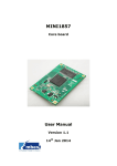
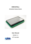
1
SBC1788 Industrial Single Board Computer User Manual Version 1.4 15th Jan 2014 Copyright Statement: SBC1788 and its related intellectual property are owned by Shenzhen Embest Technology Co., Ltd. Shenzhen Embest Technology has the copyright of this document and reserves all rights. Any part of the document should not be modified, distributed or duplicated in any approach and form without prior written permission issued by Embest Technology Co., Ltd. Revision History: Version Date Description 1.0 06/08/2012 Original Version 1.1 29/11/2012 First Revision 1.2 14/06/2013 Second Revision 1.3 11/10/2013 Third Revision 1.4 15/01/2014 Localisation Table of Contents 1 Product Overview .............................................................. 1 1.1 Introduction ....................................................................1 1.2 Kit Contents ....................................................................1 1.3 Board Interfaces ..............................................................2 1.4 System Diagram ..............................................................3 1.5 Physical Dimensions .........................................................4 2 Hardware Features ............................................................ 5 2.1 Processor .......................................................................5 2.2 Interfaces .......................................................................5 2.3 Operational Parameters ....................................................6 3 Hardware Details ............................................................... 7 3.1 CPU Introduction .............................................................7 3.2 Interface Introduction ......................................................7 3.2.1 Power Jack ................................................................................ 7 3.2.2 RS232 Interface ........................................................................ 7 3.2.3 Ethernet Interface...................................................................... 8 3.2.4 USB Host Interface .................................................................... 9 3.2.5 USB Device Interface ................................................................. 9 3.2.6 TF Card Slot .............................................................................. 9 3.2.7 LCD Interface .......................................................................... 10 3.2.8 JTAG Interface ........................................................................ 12 3.2.9 PWM Interfaces ....................................................................... 13 3.2.10 SPI Interfaces ........................................................................ 14 3.2.11 UART & ADC/DAC Interfaces.................................................... 14 3.2.12 GPIO & I2C Interfaces ............................................................ 15 3.2.13 CAN & RS485 Interfaces ......................................................... 16 3.2.14 Buttons ................................................................................. 17 3.2.15 LED Indicators ....................................................................... 17 4 Preparations .................................................................... 18 4.1 Configuring HyperTerminal ............................................. 18 4.2 Configuring the Network ................................................. 20 4.3 Installing Keil MDK......................................................... 24 4.4 Installing IAR EWARM .................................................... 29 4.5 Installing Flash Magic (Optional) ...................................... 33 5 Software Development Process ....................................... 38 5.1 Development Based on the Keil MDK ................................ 38 5.1.1 Creating and Compiling a New Project ........................................ 38 5.1.2 Programming and Debugging .................................................... 43 5.2 Development Based on IAR EWARM ................................. 47 5.2.1 Creating New Project Compiling ................................................. 47 5.2.2 Programming and Debugging .................................................... 53 5.3 In System Programming ................................................. 55 5.3.2 Create a HEX file with MDK-ARM. ............................................... 55 5.3.3 Create HEX file with IAR EWARM................................................ 56 5.3.4 Flash Magic ............................................................................. 56 6 Software Examples .......................................................... 59 6.1 Basic Example Programs for Peripherals ........................... 59 6.1.2 LCD_Display Program ............................................................... 63 6.1.3 LCD_Touch Program................................................................. 65 6.1.4 USB_MassStorage Program ....................................................... 66 6.1.5 USB_VirtualCom Program ......................................................... 67 6.1.6 USB-HostLite Program .............................................................. 68 6.1.7 Emac_EasyWeb Program .......................................................... 69 6.1.8 UART_Autobaud Program .......................................................... 70 6.1.9 Uart_Rs485Master & Uart_Rs485Slave Programs ......................... 71 6.1.10 Emc_NandFlashDemo Program ................................................ 72 6.1.11 Emc_SdramDemo Program ..................................................... 74 6.1.12 RTC_Calendar Program ........................................................... 75 6.1.13 Can_Aflut Program ................................................................. 76 6.1.14 DMA_Flash2Ram Program ....................................................... 78 6.1.15 Wdt_Reset Program ............................................................... 79 6.1.16 Timer_MatchInterrupt Program ................................................ 80 6.1.17 Systick_10msBase Program .................................................... 81 6.1.18 NVIC Program ....................................................................... 82 6.1.19 PWR_DeepSleep Program........................................................ 83 6.1.20 GPIO_LedBlinky Program ........................................................ 83 6.1.21 Pwm_SingleEdge Program ....................................................... 84 6.1.22 Mci_Fatfs_v008a Program ....................................................... 84 6.1.23 SSP_LCD_Touch Program........................................................ 86 6.1.24 ADC_Polling Program .............................................................. 87 6.1.25 Dac_SineWave Program .......................................................... 88 6.1.26 BOD Program ........................................................................ 89 6.1.27 Crc_Demo Program ................................................................ 89 6.1.28 IAP Program .......................................................................... 91 6.2 Application Programs ..................................................... 92 1.1.1 SBC1788-emWin512 Program ................................................... 92 6.2.2 httpraw_sa Program ................................................................. 93 6.2.3 tcpecho_sa Program ................................................................. 94 6.2.4 SBC1788-uCOSII-uCGUI Program .............................................. 96 6.2.5 SBC1788-uCOS-II-v2.86 Program .............................................. 97 7 Function Test ..................................................................... 1 Appendix 1: ESD Precautions & Handling Procedures ........... 2 Appendix 2: Technical support & Warranty .......................... 3 2.1 Technical support service ..................................................3 2.2 Maintenance service clause ...............................................4 2.3 Basic guidelines for protection and maintenance of LCDs ......5 2.4 Value Added Services .......................................................6 1 Product Overview 1.1 Introduction The SBC1788 is an industrial single board computer designed by Embest Technology based on the LPC1788FBD208 - a 32-bit ARM Cortex-M3 processor from NXP. It is built to industrial standards with features including: support for real-time operating systems, good EMC performance, and abundant interfaces such as UART, I2C, SPI, PWM, AD, and DA. In addition, the CD-ROM provided along with the SBC1788 contains drivers and example programs for all the on-board devices, helping users start their evaluation and development quickly and easily. The SBC1788 is suited for a wide scope of applications and can meet the requirements in many different fields including: Instrumentation, Home automation, Medical diagnosis, Motor control. 1.2 Kit Contents SBC1788 Cross-Over Serial Cable (DB9, 150CM) Cross-Over Network Cable (150CM) USB A Male to MINI USB B Male Cable 12V/1.25A Power Adaptor Four Hex Head Cap Screws with four Brass Tube Plugs CD-ROM Optional LCD Touch-Screen (4.3” with 480x272 resolution or 7” with 800x480 resolution) Page | 1 1.3 Board Interfaces Figure 1: SBC1788 Board Interfaces Page | 2 1.4 System Diagram Figure 2: SBC1788 System Block Diagram Block Description Interface modules of CPU Chips or spare solder pads on the board Interfaces on the board Page | 3 1.5 Physical Dimensions Figure 3: SBC1788 Hardware Dimensions Top Layer Component HeightMAX = 13 mm Bottom Layer Component HeightMAX = 3 mm Board Thickness =1.6mm, 6 layer PCB Page | 4 2 Hardware Features 2.1 Processor NXP 32-bit ARM Cortex-M3 LPC1788FBD208 On-Board Memory: o 128MB NAND Flash o 32MB SDRAM o 4MB SPI Flash (spare solder pads) o 2Kb EEPROM (spare solder pads) 2.2 Interfaces LCD Touch-Screen Interface: o Supports 4.3” (480×272) and 7” (800×480) TFT LCDs o Supports 4-wire resistive touch-screen o 16bit RGB565 mode 4 serial interfaces: UART0: 3-wire serial interface from DB9 male connector with RS232 level UART1: 5-wire serial interface from DIP connector with default TTL level which can be customized as RS232 level UART3: 3-wire serial interface from DIP interface with default RS232 level which can be customized as TTL level UART4: 3-wire serial interface from DIP interface with default TTL level which can be customized as RS232 level 1-channel RS485 Serial port (brought out by Phoenix Connector) USB 2.0 host interface at 2Mbps USB 2.0 host/device interface at 12Mbps 10/100 Mbps Ethernet interface Page | 5 TF card interface CAN2.0B interface 2 user custom buttons, 1 reset button, 1 ISP button 20-pin standard JTAG debugging interface buzzer 6-channel PWM interface 3-channel ADC interface DAC interface SPI interface I2C interface 18 separated GPIO interfaces 5×5 matrix keypad interface External 12V power jack high-precision RTC interface 2 WDT in chip and an on-board spare interface for external hardware WDT Power indicator USB Device FS indictor USB Host FS indicator 4 user customisable indicators 2.3 Operational Parameters Dimensions: 120x87mm (6-layer PCB) Operating Temperature: -40 ~ +85°C Storage Temperature: -40 ~ +85°C Operating Humidity: 0% ~ 90% (Non-Condensing) Power Supply: 12V/1.25A Electric Standards: CE, FCC and CCC Page | 6 3 Hardware Details This chapter will give you an overview of the product hardware system by introducing the CPU and interfaces used on the SBC1788. 3.1 CPU Introduction The SBC1788 uses an LPC1788FBD208 from NXP – a low-power ARM Cortex-M3 MCU with high performance-price ratio. This MCU works at a frequency of up to 120MHz and integrates an LCD image controller, 512 KB of flash memory, 96KB of SRAM, 4KB of EEPROM and abundant peripherals including Ethernet, USB device/host/OTG, 5 UARTs, 3 SPI/SSPs, 3 I2Cs and 165 GPIOs. 3.2 Interface Introduction The SBC1788 provides many different on-board interfaces such as RS232, Ethernet, USB host/OTC, TF card and LCD interfaces. This section will give you brief introductions for each of these interfaces. 3.2.1 Power Jack J1 Pins Definitions Descriptions 1 +12V Power supply +12V/1.25A 2 GND Grounded 3 GND Grounded 3.2.2 RS232 Interface COM1 Pins Definitions Descriptions 1 NC NC 2 RXD Receive data 3 TXD Transit data Page | 7 COM1 Pins Definitions Descriptions 4 NC NC 5 GND GND 6 NC NC 7 NC NC 8 NC NC 9 NC NC 3.2.3 Ethernet Interface CON10 Pins Definitions Descriptions 1 TX+ TX+ output 2 TX- TX- output 3 RX+ RX+ input 4 CT CT 5 CT CT 6 RX- RX- input 7 NC NC 8 SHIELD Shield 9 LED1 LINK LED 10 VDD3V3 3.3V Power for LED 11 LED2 SPEED LED 12 VDD3V3 3.3V Power for LED 13 4&5 Connect to shield 14 7&8 Connect to shield Page | 8 CON10 Pins Definitions Descriptions 15 NC NC 16 NC NC 3.2.4 USB Host Interface CON2 Pins Definitions Descriptions 1 VBUS +5V 2 D- USB Data- 3 D+ USB Data+ 4 GND GND 3.2.5 USB Device Interface CON1 Pins Definitions Descriptions 1 VBUS +5V 2 D- USB Data- 3 D+ USB Data+ 4 ID USB ID 5 GND GND 3.2.6 TF Card Slot CON3 Pins Definitions Descriptions 1 DAT2 Card data 2 2 DAT3 Card data 3 Page | 9 CON3 Pins Definitions Descriptions 3 CMD Command Signal 4 VDD VDD 5 CLK Clock 6 VSS VSS 7 DAT0 Card data 0 8 DAT1 Card data 1 9 CD Card detect 3.2.7 LCD Interface CON9 Pins Definitions Descriptions 1 GND GND 2 DCLK DCLK 3 HSYNC HSYNC 4 VSYNC VSYNC 5 GND GND 6 RST RST(Reserved) 7 R3 Red data input 8 R4 Red data input 9 R5 Red data input 10 R6 Red data input 11 R7 Red data input 12 GND GND 13 G2 Green data input Page | 10 CON9 Pins Definitions Descriptions 14 G3 Green data input 15 G4 Green data input 16 G5 Green data input 17 G6 Green data input 18 G7 Green data input 19 GND GND 20 GPIO_0 GPIO(Reserved) 21 B3 Blue data input 22 B4 Blue data input 23 B5 Blue data input 24 B6 Blue data input 25 B7 Blue data input 26 GND GND 27 DEN Display enable 28 VDD3V3 +3.3V power supply 29 VDD3V3 +3.3V power supply 30 GPIO_1 I2C_SCL(Reserved) 31 GPIO_2 I2C_SDA(Reserved) 32 Y+ Terminal of touch panel 33 X- Terminal of touch panel 34 Y- Terminal of touch panel 35 X+ Terminal of touch panel 36 PWREN LCD power enable Page | 11 CON9 Pins Definitions Descriptions 37 VDD5V +5V power supply 38 PWM 39 VDD5V +5V power supply 40 VDD12V +12V power supply LED Dimming Control by PWM Signal 3.2.8 JTAG Interface CON5 Pins Definitions Descriptions 1 VTREF +3.3V power supply 2 VSUPPLY +3.3V power supply 3 NTRST Test system reset 4 GND GND 5 TDI Test data input 6 GND GND 7 TMS Test mode select 8 GND GND 9 TCK Test clock 10 GND GND 11 RTCK GND 12 GND GND 13 TDO Test data output 14 GND GND 15 NSRST Test system reset Page | 12 CON5 Pins Definitions Descriptions 16 GND GND 17 DBGRQ Connect to GND 18 GND GND 19 DBGACK Connect to GND 20 GND GND 3.2.9 PWM Interfaces CON11 Pins Definitions Descriptions 1 P3_22 P3[22] 2 VDD3V3 +3.3V power supply 3 PWM1_1 PWM1[1] 4 PWM1_2 PWM1[2] 5 PWM1_3 PWM1[3] 6 PWM1_4 PWM1[4] 7 PWM1_5 PWM1[5] 8 PWM1_6 PWM1[6] 9 P3_23 P3[23] 10 GND GND Page | 13 3.2.10 SPI Interfaces CON12 Pins Pins Pins 1 SPI0_MOSI SPI0_MOSI 2 VDD3V3 +3.3V power supply 3 P3_20 P3[20] 4 P3_19 P3[19] 5 SPI0_SSEL SPI0_SSEL 6 P3_14 P3[14] 7 SPI0_SCK SPI0_SCK 8 P2_25 P2[25] 9 SPI0_MISO SPI0_MISO 10 GND GND 3.2.11 UART & ADC/DAC Interfaces CON7 Pins Definitions Descriptions 1 VDD5V +5V power supply 2 VDD3V3 +3.3V power supply 3 ADC0_IN0 ADC0_IN0 4 ADC0_IN2 ADC0_IN2 5 ADC0_IN1 ADC0_IN0 6 DAC_OUT DAC_OUT 7 P1_05 P1[5] 8 GND GND 9 TXD3 UART3_ TXD Page | 14 CON7 Pins Definitions Descriptions 10 TXD1 UART1_ TXD 11 RXD3 UART3_ RXD 12 RXD1 UART1_ RXD 13 P1_13 P1[13] 14 P5_02 P5[02] 15 TXD4 UART4_ TXD 16 CTS1 UART1_CTS1 17 RXD4 UART4_ RXD 18 RTS1 UART1_RTS1 19 GND GND 20 GND GND 3.2.12 GPIO & I2C Interfaces CON8 Pins Definitions Descriptions 1 VDD5V 5V power supply 2 VDD3V3 +3.3V power supply 3 I2C0_SCL I2C0_SCL 4 I2C2_SCL I2C2_SCL 5 I2C0_SDA I2C0_SDA 6 I2C2_SDA I2C2_SDA 7 P4_21 P4[21] 8 GND GND 9 P4_22 P4[22] Page | 15 CON8 Pins Definitions Descriptions 10 P0_04 P0[04] 11 P4_23 P4[23] 12 P0_05 P0[05] 13 P4_26 P4[26] 14 P0_18 P0[18] 15 P4_27 P4[27] 16 P3_21 P3[21] 17 P4_28 P4[28] 18 GND GND 19 GND GND 20 GND GND 3.2.13 CAN & RS485 Interfaces CON4 Pins Definitions Descriptions 1 +12V Power 2 GND_IN GND 3 CAN1H CAN1_H 4 CAN1L CAN1_L 5 485A RS485 6 485B RS485 Page | 16 3.2.14 Buttons S1 SW1~SW3 Pins Definitions Descriptions S1 RESET System SW1 USER1 User-defined SW2 USER2 User-defined SW3 ISP ISP 3.2.15 LED Indicators LED1~4 LEDs Definitions Descriptions LED1 P4[15] User LED2 P4[16] User LED3 P4[17] User LED4 P4[18] User Page | 17 4 Preparations Before you get started with software development, you need to make a series of preparations including configuring HyperTerminal, setting up a network, and installing a Keil MDK or IAR EWARM integrated development environment. The following contents will show you how to complete the installation and configuration processes on a PC running Windows XP. 4.1 Configuring HyperTerminal 1. Select: Start All Programs Accessories Communications HyperTerminal On your PC’s desktop to open a HyperTerminal window as shown below; Figure 4: New HyperTerminal Window Page | 18 Enter a name for the new HyperTerminal in the Name textbox, and then click OK; 2. Select the serial interface used to connect to the SBC1788 from the Connect using dropdown menu as shown in the window to the right, OK; and then click Figure 5: Select Serial Interface 3. Configure the serial interface according to the configurations in the window shown to the right, and then click OK; Figure 6: Configure Serial Interface Page | 19 4. The window below indicates that the configuration has been set up successfully; HyperTerminal Figure 7HyperTerminal Is Connected 4.2 Configuring the Network 1. Click Start Control Panel Network and Internet Network Connections On your PC’s desktop, and then double-click Local Area Connection to open the window as shown right; Then click Properties to open the Local Area Connection Properties window; Figure 8: Local Area Connection Status Page | 20 2. Double-click Internet Protocol (TCP/IP) as in the window shown to the right; Figure 9: Internet Protocol TCP/IP 3. Click Advanced in the window shown to the right; Figure 10: Select Advanced Note: Please ensure the option Use the following IP address is checked, and then click Advanced to specify additional IP addresses for PC. Page | 21 4. Click Add in the address block in window shown below; IP the Figure 11: Click Add 5. Enter an IP address that is in the same network segment as the SBC1788 (the SBC1788s default IP address is 192.168.0.232), e.g. 192.168.0.40 in the pop-up window, and then enter a subnet mask and click Add; Figure 12: Enter an IP Address Note: You can use any IP address from 192.168.0.1 to 192.168.0.254 except 192.168.0.100, because this address will cause IP conflict when the Ethernet example program is running. Page | 22 6. The window shown below indicates that a new IP address has been added to the PC; Now click OK to finish the configuration; Figure 13: Click OK Page | 23 4.3 Installing Keil MDK Development on the LPC1788 requires version 4.20 or higher of the Keil MDK. All the MDK projects contained in the CD-ROM provided along with the board are created in MDK 4.22a. You can download the latest version from Keil’s official website: www.keil.com. The following content will show you how to install the Keil MDK integrated development environment using MDK 4.22a as an example. 1. Launch the installation package to open the window shown below; Figure 14: Installation Program 2. Click Next to continue; 3. Check I agree to all the terms of the preceding License Agreement and click Next in the window shown below; Page | 24 Figure 15: License Agreement 4. Click Browse in the window shown below to specify an installation path, and then click Next; Figure 16: Specify the installation path 5. Enter user information such as name, company name and email, and then click Next to start file installation process; Page | 25 Figure 17: Enter User Information 6. After file installation is completed, keep the default settings unchanged in the window shown below and click Next; Figure 18: Installing Example Projects 7. Keep the default settings unchanged in the window shown below and click Finish; Page | 26 Figure 19: Installing ULINK Pro Driver 8. Click Continue Anyway in the pop-up window as shown below; Figure 20: Click Continue Anyway 9. The installation window as shown below will automatically after ULINK Pro driver is installed; be closed Page | 27 Figure 21: Installing ULINK Pro Driver 10. Now the installation of the Keil MDK integrated development environment has been completed successfully. Page | 28 4.4 Installing IAR EWARM Development on the LPC1788 requires version 6.20 or higher of IAR EWARM. All the EWARM projects contained in the CD-ROM provided with the board are created by using IAR EWARM 6.40.2. You can download the latest version from IAR’s official website: www.iar.com. The following content will show you how to install an IAR EWARM integrated development environment, using IAR EWARM 6.40.2 as an example. 1. Double-click the installation file of IAR EWARM to open the installation interface as shown below; Figure 22: IAR EWARM Installation Interface 2. Click Install IAR Embedded Workbench; 3. Click Next in the following window to continue installation; Page | 29 Figure 23: Click Next 4. Select the radio button I accept the terms of the license agreement, and the click Next in the following window; Figure 24: License Agreement 5. Enter your name and your company’s name, as well as the license number in the following window, and then click Next; Page | 30 Figure 25: Enter User Information 6. Copy your license key into the License Key textbox, or click Browse to specify the path where the license key is saved, and then click Next; Figure 26: Enter License Key 7. Click Change in the following window to specify installation path, and then click Next; Page | 31 Figure 27: Select Installation Path 8. The following window allows you select a folder in which the software icon is contained; You may keep the default settings unchanged and click Next; Figure 28: Select Software Icon Location 9. Click Install in the following window to start the installation process; Page | 32 Figure 29: Select Install 10. Click Finish in the following window to finish the installation process; Figure 30: Installation is Complete 4.5 Installing Flash Magic (Optional) Flash Magic is a free downloadable tool designed to run on a Windows based PC. It is used for downloading programs to NXP’s Flash MCU by Page | 33 using serial or Ethernet protocols. The supported chips include the ARM, C51 and LPC families. Please visit: http://www.flashmagictool.com/supporteddevices.html To view all the supported target devices. Note: If you don’t want to use this tool to download programs, please ignore this section. 1. Download Flash Magic from: http://www.flashmagictool.com 2. Double-click the installation file to open the window as shown below; Figure 31: Flash Magic Installation Window 3. Click Next to continue; 4. Select I accept the agreement in the window shown below and click Next; Page | 34 Figure 32: License Agreement 5. Click Browse in the window shown below to specify an installation path, and then click Next; Figure 33: Installation Path 6. Click Browse in the window shown below to specify the position of the Flash Magic shortcut icon in the Start Menu, and then click Next; Page | 35 Figure 34: Position of Short Cut Icon 7. Select the options Create a desktop icon and Create a Quick Launch icon according your requirements, and then click Next: Figure 35: Create Icons 8. Click Install in the window shown below to start installation; Page | 36 Figure 36: Start Installation 9. The window shown below indicates that installation has been completed; If Launch Flash Magic is checked, Flash Magic will be launched immediately after you click Finish; If View the Release Notes is checked, the software release notes will be opened immediately after clicking Finish; Figure 37: Installation Finished Page | 37 5 Software Development Process After all the preparations are completed, the development process can be started. This chapter will introduce how to conduct software development under two different environments, Keil MDK and IAR EWARM by using the development of NXP’s LPC1788 processor as an example. Note: Development on LPC1788 requires version 4.20 or higher of Keil MDK or, version 6.20 or higher of IAR EWARM; this document uses Keil MDK 4.60 and IAR EWARM 6.40.2. 5.1 Development Based on the Keil MDK The following content is composed of two parts which introduce how to create and compile MDK projects, as well as program and debug the compiled files. 5.1.1 Creating and Compiling a New Project 1. Click Start All Programs Keil uVision4 on the PC’s desktop to open a uVision4 window as shown right; Figure 38: uVision 4 Window Page | 38 2. Click Project > New uVision Project on the menu bar of the uVision4 window to open the following window; Figure 39: Create a New Project 3. Specify the storage path and name for the new project (e.g. Target1), and then click Save; 4. Select NXP (founded by Philips) > LPC4357 in the tree view of the window shown below, and then click OK; Figure 40: CPU Selection Page | 39 5. The following pop-up window prompts you to determine if NXP LPC177x_8x Start Code should be copied to the project folder; “Yes” is recommended; Figure 41: Adding Start Code 6. Right-click the project Target1 in the tree view on the left part of the following window and select Add Group to create different groups to which the corresponding code will be added, for example a group named “Drivers” to which the EDM1070xx’s driver source files will be added later; Figure 42: Add New Groups Page | 40 7. After all the groups are created, right-click each group and select Add Files to Group… to add relevant source code; Figure 43: Adding Source Code to Groups 8. Right-click Target1 in the tree view of the uVision4 window and select Options for Target ‘Target1’, and then select C/C++ tab in the pop-up window as shown below; Figure 44: C/C++ Tab Specify the paths where the head files are saved in the Include Paths textbox, and then click OK; Page | 41 9. Click the Rebuild button: on the tool bar as shown in the following window to start compiling all the files; Figure 45: Click Rebuild The information box at the bottom of the window shows that compilation has completed successfully. Now the process of creating and compiling a project is finished. Page | 42 5.1.2 Programming and Debugging You can now proceed with flash programming and debugging by following the steps listed below; 1. Right-click Target1 in the tree view of uVision4 window and select Options for Target ‘Target1’, and then select the Utilities tab in the pop-up window as shown below; Figure 46: Utilities Tab 2. Check the radio button Use Target Device for Flash Programming and the checkbox Update Target before Debugging, select ULINK Cortex Debugger in the corresponding drop-down menu, and then click Settings; 3. Select the Flash Download tab in the pop-up window as shown right; Figure 47: Flash Download Settings Page | 43 Click Add at the bottom of the window; Note: The purpose of this step is to add necessary flash programming algorithms. If LPC17xx IAP 512kB Flash is already in the list of Programming Algorithms, there is no need to add it again and you can jump to step 4. 4. Select LPC17xx IAP 512Kb Flash in the pop-up window as shown below and click Add; Figure 48: Add a Flash Programming Algorithm 5. Click OK twice to go back to the uVision4 window; Page | 44 6. Click the Download button: on the tool bar of the uVision4 window to start flash programming; Figure 49: Start Flash Programming 7. After programming is done, right-click Target1 in the tree view of the uVision4 window and select Options for Target ‘Target1’, and then select the Debug tab in the pop-up window as shown below; Figure 50: Debug Settings Page | 45 8. Check the radio button Use at the top right of the Debug tab and select ULINK Cortex Debugger in the corresponding drop-down menu, and then click OK; 9. Click the Debug button: on the tool bar of the uVision4 window as shown below to start online debugging; Figure 51: Start Debugging Page | 46 5.2 Development Based on IAR EWARM The following content is composed of two parts which introduce how to create and compile IAR projects, as well as program and debug the compiled files. 5.2.1 Creating New Project Compiling 1. Launch the software to open the IAR Embedded Workbench IDE window as shown below; Figure 52: IAR Embedded Workbench Window 2. Select Project > Create new project on the menu bar of the above window to create a new project; Page | 47 3. Select Empty project in the following pop-up window, and then click OK; Figure 53: Select an Empty Project 4. Select a path to save the new project in the following pop-up window, and then click Save; Figure 54: Set New Project Save Path Page | 48 5. Right-click the project name on the left side of the IAR Embedded Workbench IDE window and select Add > Add Group to create different groups to which the corresponding code will be added, for example a group named “Drivers” to which driver source files will be added later; Figure 55: Create New Groups 6. After all the necessary groups are added, right-click each group and select Add > Add Files to add relevant source code; Figure 56: Add Source Code to Groups Page | 49 7. After all the files are added, right-click the project name and select Options to open the window below; Figure 57: Project Options Window 8. Under the Target tab, check the radio button Device and click the button on the right, and then select NXP > LPC1700 > NXP LPC1788 in the pop-up menu; Page | 50 9. Click C/C++ Compiler on the left side of the window and select the Preprocessor tab in the right part of the window, and then add the paths of the head files to the Additional include directories textbox; Figure 58: Head File Paths 10. Click Linker on the left side of the window and select the Config tab in the right part of the window, and then check the Override default checkbox and click the button as shown below to specify the paths of the linker configuration files; 11. Click OK to save settings; Page Figure 59:Linker Configuration File Locations | 51 12. Right-click the project name on the left side of the IAR Embedded Workbench IDE window and select Rebuild All to recompile the project; Figure 60: Recompile the Project 13. Now the creation and compilation of a new project has been completed successfully. Page | 52 5.2.2 Programming and Debugging 1. You can now proceed with flash programming and debugging by following the steps listed below; 2. Right-click the project name on the left side of the IAR Embedded Workbench IDE window and select Options to open the following window; Figure 61: Project Options Window 3. Click Debugger on the left side of the window and select the Setup tab in the right part, and then select J-Link/JTrace in the Driver dropdown menu; Figure 62: Downloading & Debugging Tool Page | 53 4. Click the Download tab and check the Verify download checkbox, and then click OK; Figure 63: Check the Verify Download Checkbox 5. Select Project > Download and Debug on the menu bar of the IAR Embedded Workbench IDE window to start downloading and debugging; Figure 64: Select Download and Debug Page | 54 5.3 In System Programming The LPC1788 contains a bootloader in ROM that can be enabled by pulling pin P2.10 low during reset. The application can then be downloaded over UART#0 (serial channel). In order to run ISP, please follow the steps below: 1. Connect a null-modem female/female RS232 cable between the DB9 connector COM1 (USART0) and the PC serial port. 2. Plug in the 12V power adapter. 5.3.2 Create a HEX file with MDK-ARM. 1. Open an MDK project, configure Target Option and select Create HEX file. 2. Rebuild the Project, generate the HEX file. 3. The HEX file is located in the \Keil\Flash subfolder of the project directory. Figure 65: Configure MDK output option Page | 55 5.3.3 Create HEX file with IAR EWARM. 1. Open an EWARM project, configure the options and select the output format. 2. Select Intel extended for output. Rebuild the Project, generate the HEX file. 3. The HEX file is located in the \EWARM\Flash\Exe subfolder of the project directory. Figure 66: Configure EWARM output option 5.3.4 Flash Magic 1. Open the Flash magic software, select Options->Advanced Options. Page | 56 Figure 67: Flash Magic Advanced Options 2. Then select the Hardware Config tab and set the T1/T2 numbers according to figure below. Figure 68: Flash Magic T1 & T2 Settings Page | 57 3. Ensure the Flash magic settings are set as below. Figure 69: Flash Magic Configuration Settings Select Device: LPC1788 COM Port: Set this according to your PC serial port Baud Rate: Set to 57600 or lower Interface: None (ISP) Oscillator: (MHz): 12.000 Hex File: Select the hex/binary file to be downloaded 4. Download the hex file Note: The ISP (SW3) button should be constantly pressed. Press the RESET button and then release the ISP (SW3) button, LPC1788 will then enter ISP mode. Click the Start icon to start downloading the hex file. After the download finishes, press the RESET button, and the MCU will start to run. Page | 58 6 Software Examples The CD-ROM provided along with the SBC1788 contains abundant example programs. All the programs are created based on the standard peripheral libraries from NXP. This chapter will introduce how to learn about the features of the LPC1788 through a variety of example programs which consist of basic and additional examples. 6.1 Basic Example Programs for Peripherals The basic example programs are saved under X:\code\LPC177x_8x_StdPeriph_Demo\Examples of the CD-ROM (where X:\ is the label of CD-ROM drive) as shown below; The folders that are saved under the same directory as Examples include BoardSupport, Core, Drive and makesection; The following numbered entries give a brief introduction of the files contained in these folders; 1. BoardSupport: The drivers for the on-board peripherals of the SBC1788 including SDRAM, NAND Flash, PhyLAN and LCD interfaces. 2. Core: CMSIS files and the startup code from NXP for MDK and IAR environments. 3. Drivers: Driver codes for peripherals of the LPC177x_8x including two folders –include and source. 4. Examples: Basic example programs for peripherals of the LPC1788 under Keil and EWARM environments. 5. Makesection: environments. Configuration files for development Page | 59 The table shown below lists all the basic example programs for peripherals and their relevant descriptions. This section will use a selection of the example programs to introduce the detailed operations. Name of Example Programs LCD_Display Descriptions Using the LCD controller of the LPC1788 to drive an LCD module LCD LCD_Touch USB_MassStorage USB USB_VirtualCom UsbHost_MassStorage Emac_EasyWeb Ethernet Emac_Raw Emac_uIP Configuring an LCD and calibrating a touchscreen A simple application of USB mass storage devices Configuring the USB device on the SBC1788 to work as a virtual serial interface Configuring the LPC1788 to work as a USB host A simple web application Testing the EMAC driver without involving a protocol layer A simple web application that involves IP, ICMP, UDP and TCP protocols UART_Autobaud UART communication under auto baud mode UART_Dma Using UART under DMA mode UART_Interrupt Using UART under interrupt mode UART_Polling Using UART under polling mode Uart_Rs485Master Host application for RS485 communication Uart_Rs485Slave Slave application for RS485 communication Emc_NandFlashDemo Writing and calibrating on-board NAND Flash UART EMC Page | 60 Name of Example Programs Emc_SdramDemo Descriptions Writing and calibrating on-board SDRAM Generating interrupts in the second counter Rtc_Alarm increment interrupts, and an alert interrupt every 10 seconds as well RTC Rtc_Calendar Configuring RTC calendar Rtc_Calibration Calibrating RTC clock Can_Aflut CAN Can_Selftest Using the function of CAN driver to configure and alter the receiving filter loot-up table Self test mode of CAN Testing GPDMA (General Purpose Direct DMA_Flash2Ram Memory Access) by data transfer from flash to RAM Wdt_Interrupt WDT Wdt_Reset Wdt_WindowMode Timer_Capture Timer_FreqMeasure Timer Using WDT to generate interrupts after a certain period of time Using WDT to generate reset signal after a certain period of time to reset MCU Generating interrupt or reset signal under WDT window mode Using the input capture function of the timer Using the timer to measure the frequency of an input signal Using timer matching to generate a certain Timer_MatchInterrupt time interval (e.g. 1 second) under interrupt mode. Systick_10msBase SYSTICK NVIC System timer generates an interrupt every 10ms Systick_Stclk System timer uses an external clock signal Nvic_Priorities Testing Tail-chaining or Late-arriving interrupt mode through NVIC priority Page | 61 Name of Example Programs Descriptions grouping Nvic_VectorTableRelocation PWR_DeepPowerDown PWR_DeepSleep Relocating vector table System enters deep power down mode and is woken up by an RTC interrupt System enters deep sleep mode and is woken up by an external interrupt PWR PWR_PowerDown PWR_Sleep GPIO_Interrupt GPIO GPIO_LedBlinky Pwm_DualEdge PWM Pwm_MatchInterrupt Pwm_SingleEdge Mci_CidCard MCI woken up by an NMI interrupt System enters sleep mode and is woken up by a WWD interrupt Using the interrupt function of the GPIO Using GPIO to receive button interrupts, drive the LED and the buzzer Generating a PWM signal under single/dual edge mode Using the PWM matching function under interrupt mode Generating a PWM signal under single edge mode Using the MCI (Multimedia Card Interface) of the LCP1788 Mci_Fatfs_v008a Using a MicroSD in the file system Mci_ReadWrite Writing and reading the MCI of the LPC1788 SSP_Dma Testing SSP under DMA mode SSP SSP_LCD_Touch ADC System enters power down mode and is ADC_Burst Configuring the touch function chip of an LCD through the SPI bus Using AD conversion under burst mode Page | 62 Name of Example Programs Descriptions Using the AD conversion function and ADC_Dma transferring AD conversion results under DMA mode ADC_Interrupt Using AD conversion under interrupt mode ADC_Polling Using AD conversion under polling mode Dac_Dma Using the DAC to generate an analog output under DMA mode DAC Dac_SineWave BOD Generating a sine wave output by using the DAC Using BOC (Brown-Out Detector) function Implementing a CRC-CCITT, CRC-16 and Crc_Demo CRC-32 calibration based on given data by using the LPC1788’s CRC function CRC Implementing CRC-32 calibration based on Crc_Dma given data under DMA mode by using the LPC1788’s CRC function Using IAP to update the space after the user IAP code in flash, and read chip information including ID, boot code version and serial number 6.1.2 LCD_Display Program 1. Connect an LCD screen to the CON9 interface (marked as “LCD & Touch” in Figure 1 on page 2) of the SBC1788 with an LCD flat cable; 2. Expand the Main branch in the tree view on the left side of the uVision4 window and double-click lcd_driver.h, and then select a definition of initialization macro on the right side according to the LCD screen size as shown below; Page | 63 Figure 70: Macro Definition for 4.3" Figure 71: Macro Definition for 7" Note: The SBC1788 supports two LCD modules, LCD6000-43T and LCD6000-70T which have a 480×272, 4.3” and an 800×480 7” screen respectively. The red line of the LCD flat cable should be on the same side as the 1st pin (marked with a triangle) of the CON9 interface. The capacitors C3, C5, C6 and C7 should be removed from the board if a 4.3” touch-screen LCD is used. 3. Power on the SBC1788 and recompile the project, and then download it to flash; 4. Reboot the SBC1788; The LCD will display 4 colour stripes – red, green, blue and yellow, as well as a light-blue round spot moving along the red stripe; Page | 64 6.1.3 LCD_Touch Program 1. Connect the LCD screen to the CON9 interface (marked as “LCD & Touch” in Figure 1 on page 2) of the SBC1788 with an LCD flat cable; 2. Expand the Main branch in the tree view on the left side of the uVision4 window and double-click lcd_driver.h, and then select a definition of initialization macro on the right side according to LCD screen size as shown below; Figure 72: Macro Definition for 4.3" Figure 73: Macro Definition for 7" Note: The SBC1788 supports two LCD modules, LCD6000-43T and LCD6000-70T which have a 480×272, 4.3” and an 800×480, 7” screen respectively. The red line of the LCD flat cable should be on the same side as the 1st pin (marked with a triangle) of the CON9 interface. The capacitors C3, C5, C6 and C7 should be removed from the board if a 4.3” touch-screen LCD is used. Page | 65 3. Power on the SBC1788 and recompile the project, and then download it to flash; 4. Reboot the SBC1788 and use a stylus to touch the points which are marked with “+” symbols on the screen to implement calibration. When please touch the screen appears on the screen, please use a stylus to touch a random point on the screen. The voltage value generated by the touching will be converted by the ADC and displayed on the screen, along with the corresponding coordinates. 6.1.4 USB_MassStorage Program 1. Connect the SBC1788 to your PC with a USB-A (M) to USB-B (M) cable and a cross-over serial cable. 2. Open a HyperTerminal window on your PC; (please refer to 4.1 Configuring HyperTerminal on page 18) 3. Power on the SBC1788 and recompile the project, and then download it to flash; 4. Reboot the SBC1788; The board will be recognized as a USB mass storage device by the PC and the LED6 indicator will light up; You can find a file named README.TXT by opening the drive LPC178x in the My Computer window on your PC as shown below; Figure 74: LPC178x Working as a USB Mass Storage Device Page | 66 6.1.5 USB_VirtualCom Program 1. Connect the SBC1788 to your PC with a USB-A (M) to USB-B (M) cable and a cross-over serial cable; 2. Open a HyperTerminal window on your PC; (refer to 4.1 Configuring HyperTerminal on page 18) 3. Power on the SBC1788 and recompile the project, and then download it to flash; 4. Reboot the SBC1788; The board will be recognized as a virtual serial device and the LED6 indicator will light up; You can find a serial device named LPC178x USB VCOM Port (COMx) under the Ports (COM & LPT) branch in the Device Manager window of your PC as shown below; Figure 75: LPC177x Working as a Serial Device Note: If the PC prompts you to install a driver, you can find the driver under X:\ code\LPC177x_8x_StdPeriph_Demo\Examples\02-USBDevice\USB_VirtualCom. (where X:\ is the label of CD-ROM drive) 5. Open a HyperTerminal window for the virtual serial device; Any characters entered in a window will be received and displayed in the other as shown below; Page | 67 Figure 76: Communication Between Serial Devices 6.1.6 USB-HostLite Program 1. Connect the SBC1788 to your PC with a cross-over serial cable and open a HyperTerminal window; 2. Copy the folder Folder and the file FILENAME_R.txt from 3. X:\code\LPC177x_8x_StdPeriph_Demo\Examples\03USBHostLite\UsbHost_MassStorage to a USB flash drive (where X:\ is the label of CD-ROM drive), and then insert the drive into the USB interface of the SBC1788; Note: Due to the uncertainty of compatibility, some USB flash drives may not work properly with this program. Please try another drive if you encounter this issue. 4. Power on the SBC1788 and recompile the project, then download it to flash; 5. Reboot the SBC1788; the HyperTerminal window will display information as shown below; *********************************************************** ********************* Hello NXP Semiconductors UART Host Lite example - MCU: LPC177x_8x - Core: ARM CORTEX-M3 - UART Communication: 115200 bps Page | 68 This example used to test USB Host function. *********************************************************** ********************* Host Initialized Connect a Mass Storage device Mass Storage device connected Copying file... Copy completed 6. Connect the USB flash drive to your PC and check the contents of the drive to see if FILENAME_R.txt has been copied to the folder Folder; 6.1.7 Emac_EasyWeb Program 1. Connect the input lead of a 10K potentiometer to a 3.3V input, and the output lead to the ADC0_IN2 pin on the SBC1788 (the 4th pin of the connector marked as UART1/3/4&DA&AD*3CH in Figure 1 on page 2), and the last one to ground; 2. Connect the SBC1788 to your PC with a cross-over network cable and a cross-over serial cable, and then open a HyperTerminal window; 3. Power on the SBC1788 and recompile the project, and then download it to flash; 4. Reboot the SBC1788; The HyperTerminal window displays the IP address 192.168.0.100 of the SBC1788; 5. Click Start > Run on your PC’s desktop, type cmd in the pop-up window, and then press Enter on your keyboard to open a command line window; Type ping 192.168.0.100 –t in the window and press Enter again to receive the information as shown below; Figure 77: Network Testing Page | 69 6. Type http://192.168.0.100 in the address bar of your Internet browser and press Enter on your keyboard to open the page as shown below; Figure 78: Potentiometer Level Display When the potentiometer is being turned, the voltage value converted by the ADC will change accordingly; 6.1.8 UART_Autobaud Program 1. Connect the SBC1788 to your PC with a cross-over serial cable and open a HyperTerminal window; 2. Power on the SBC1788 and recompile the project, and then download it to flash; 3. Reboot the SBC1788 and type a in HyperTerminal window as shown below to enter auto baud mode; AutoBaudrate Status: Synchronous! *********************************************************** ********************* Hello NXP Semiconductors UART Auto-Baudrate example - MCU: LPC177x_8x - Core: ARM CORTEX-M3 - UART Communication: 115200 bps This example used to test UART component with autobaudrate function. It will adjust its rate to synchronize with the sending data Page | 70 + Please press any key to be echoed + Press 'r' to re-show the welcome string + Press ESC to terminate *********************************************************** ********************* a Type any character and the HyperTerminal window will respond with the same character; Note: Type r to show the welcome string again; Press ESC on your keyboard to terminate the program. 6.1.9 Uart_Rs485Master & Uart_Rs485Slave Programs 1. Connect the fifth and sixth pins of the RS485 interface (marked as “RS485” in Figure 1 on page 2) on an SBC1788 to the same pins on another SBC1788 as shown below; Figure 79: Connection Between Two SBC1788 2. Connect one of the boards to a PC with a cross-over serial cable and open a HyperTerminal window; 3. Power on both boards and recompile the Uart_Rs485Master and Uart_Rs485Slave projects, and then download them to the flash memories of host (the board with cross-over serial cable) and slave respectively; 4. Reboot both SBC1788s; The HyperTerminal will display information as shown below; Hello NXP Semiconductors Page | 71 RS485 demo in Master mode Sending to A... Receive: ACK Sending to B... Receive: No Dev Reply …… Sending to A... Receive: ACK Sending to B... Receive: No Dev Reply 6.1.10 Emc_NandFlashDemo Program 1. Connect the SBC1788 to your PC with a cross-over serial cable and open a HyperTerminal window; 2. Power on the SBC1788 and recompile the project, and then download it to flash; 3. Reboot the SBC1788; the HyperTerminal window will display information as shown below; *********************************************************** ********************* Hello NXP Semiconductors # NANDFLASH K9F1G08U0B testing - MCU: LPC177x_8x - Core: Cortex-M3 - UART Communication: 115200 bps Write and verify data with on-board NAND FLASH *********************************************************** ********************* Init NAND Flash... Read NAND Flash ID: ECF19500 Checking valid block... Erase entire NAND Flash... Write a block of 2K data to NAND Flash... Read back a block of 2K data from NAND Flash... Verify data... Verifying complete! Testing terminated! Page | 72 Page | 73 6.1.11 Emc_SdramDemo Program 1. Connect the SBC1788 to your PC with a cross-over serial cable and open a HyperTerminal window; 2. Power on the SBC1788 and recompile the project, and then download it to flash; 3. Reboot the SBC1788; the HyperTerminal window will display information as shown below; *********************************************************** ********************* Hello NXP Semiconductors Test SDRAM mt48lc16m16A2P with LPC1788 EMC - MCU: LPC177x_8x - Core: Cortex-M3 - UART Communication: 115200 bps Write and verify data with on-board SDRAM *********************************************************** ********************* Init SDRM... Clear content of SDRAM… Writing in 8 bits format... Verifying data... Continue writing in 16 bits format... Clear content of SRAM... Writing in 16 bits format... Verifying complete! Testing terminated! Page | 74 6.1.12 RTC_Calendar Program 1. Install a CR1220 battery in the RTC battery holder (marked as RTC in Figure 1 on page 2) on the SBC1788; 2. Connect the SBC1788 to your PC with a cross-over serial cable and open a HyperTerminal window; 3. Power on the SBC1788 and recompile the project, and then download it to flash; 4. Reboot the SBC1788; the HyperTerminal window will display information as shown below; *********************************************************** ********************* Hello NXP Semiconductors RTC Set Example: - MCU: LPC177x_8x - Core: ARM CORTEX-M3 - UART Communication: 115200 bps A simple RTC Calendar example. To generate interrupt in Second Counter Increment Interrupt (1s) *********************************************************** ********************* Current time set to: 02012/003/013 016:015:030 02012/003/013 016:015:031 02012/003/013 016:015:032 02012/003/013 016:015:033 02012/003/013 016:015:034 02012/003/013 016:015:035 02012/003/013 016:015:036 02012/003/013 016:015:037 02012/003/013 016:015:038 02012/003/013 016:015:039 02012/003/013 016:015:040 Page | 75 6.1.13 Can_Aflut Program 1. Connect the third and fourth pins of the CAN interface (marked as CAN2.0B in Figure 1 on page 2) on a SBC1788 to the same pins on another SBC1788 as shown below; Figure 80: CAN Connection Diagram 2. Connect one SBC1788 to your PC with a cross-over serial cable and open a HyperTerminal window; 3. Power on both boards and recompile the project, and then download it to their flash memories; 4. Reboot both SBC1788s; The information as shown below; HyperTerminal displays *********************************************************** ********************* Hello NXP Semiconductors CAN AFLUT example: - MCU: LPC17xx - Core: ARM CORTEX-M3 - UART Communication: 115200 bps Use 2 CAN peripherals: CAN1&CAN2 to transfer data This example tests full Acceptance Filter operation and load/remove AFLUT entry dynamically functions *********************************************************** ********************* Test Acceptance Filter function... Init message finished!!! Setup AF: SUCCESSFUL!!! Message ID: 0x00000001 Message length: 0x00000008 BYTES Page | 76 Message type: DATA FRAME Message format: STANDARD ID FRAME FORMAT Message dataA: 0x78787878 Message dataB: 0x21212121 Message ID: 0x00000008 Message length: 0x00000008 BYTES Message type: DATA FRAME Message format: STANDARD ID FRAME FORMAT Message dataA: 0x15151515 Message dataB: 0x36363636 …… Sending finished !!! display received messages... Message ID: 0x00000001 Message length: 0x00000008 BYTES Message type: DATA FRAME Message format: STANDARD ID FRAME FORMAT Message dataA: 0x78787878 Message dataB: 0x21212121 …… messages Check OK... Page | 77 6.1.14 DMA_Flash2Ram Program 1. Connect the SBC1788 to your PC with a cross-over serial cable and open a HyperTerminal window; 2. Power on the SBC1788 and recompile the project, and then download it to flash; 3. Reboot the SBC1788; the HyperTerminal window will display information as shown below; *********************************************************** ********************* Hello NXP Semiconductors GPDMA FLASH to RAM example - MCU: LPC177x_8x - Core: ARM CORTEX-M3 - UART Communication: 115200 bps This example used to test GPDMA function by transfer data from Flash to RAM memory *********************************************************** ********************* Start transfer on channel 000 Buffer Check success! Demo terminated! Page | 78 6.1.15 Wdt_Reset Program 1. Connect the SBC1788 to your PC with a cross-over serial cable and open a HyperTerminal window; 2. Power on the SBC1788 and recompile the project, and then download it to flash; 3. Reboot the SBC1788; the HyperTerminal window will display information as shown below; *************************************************************** ***************** This Welcome Screen below will executive after reset event Hello NXP Semiconductors Watch dog timer reset when timeout demo - MCU: LPC177x_8x - Core: ARM CORTEX-M3 - UART Communication: 115200 bps Use WDT with Internal RC OSC, reset mode, timeout = 5 seconds To reset MCU when time out. After reset, program will determine what cause of last reset time (external reset or WDT time-out) The program is currently working in FLASH mode *************************************************************** ***************** Last MCU reset caused by External! *************************************************************** ***************** This Welcome Screen below will executive after reset event Hello NXP Semiconductors Watch dog timer reset when timeout demo - MCU: LPC177x_8x - Core: ARM CORTEX-M3 - UART Communication: 115200 bps Use WDT with Internal RC OSC, reset mode, timeout = 5 seconds To reset MCU when time out. After reset, program will determine what cause of last reset time (external reset or WDT time-out) The program is currently working in FLASH mode *************************************************************** ***************** Last MCU reset caused by WDT TimeOut! Page | 79 6.1.16 Timer_MatchInterrupt Program 1. Connect the SBC1788 to your PC with a cross-over serial cable and open a HyperTerminal window; 2. Power on the SBC1788 and recompile the project, and then download it to flash; 3. Reboot the SBC1788; the HyperTerminal window will display information as shown below; *********************************************************** ********************* Hello NXP Semiconductors Timer Match Interrupt demo - MCU: LPC177x_8x - Core: ARM CORTEX-M3 - UART Communication: 115200 bps Use timer x toggle MATx.0 at frequency 1Hz *********************************************************** ********************* Match interrupt occur... Match interrupt occur... Match interrupt occur... Match interrupt occur... Match interrupt occur... A 0.5Hz spare wave can be viewed using an oscilloscope detecting the output signal from CON11.4 (the 4th pin of the interface marked as PWM*6CH &GPIO in Figure 1 on page 2) on the SBC1788. Page | 80 6.1.17 Systick_10msBase Program 1. Connect the SBC1788 to your PC with a cross-over serial cable and open a HyperTerminal window; 2. Power on the SBC1788 and recompile the project, and then download it to flash; 3. Reboot the SBC1788; A 100Hz spare wave can be viewed using an oscilloscope as shown below, detecting the output signal from CON12.4(the 4th pin of the interface marked as SPI & GPIO in in Figure 1 on page 2) on the SBC1788; Figure 81: Oscilloscope Showing Square Waves Page | 81 6.1.18 NVIC Program 1. Modify the macro definition of INT_MODE as shown in the following uVision4 window to test Tail-Chaining or Latearriving interrupt mode; Figure 82: Modify INT_MODE Macro Definition 2. Recompile the project after modification, and then download it to flash; 3. Reboot the SBC1788 to run the program; The testing processes under two modes are listed below; Tail-Chaining interrupt mode: When the LED2 indicator is blinking (triggered by ADC interrupt), press the SW3 button to generate an INT0 interrupt, and LED1 will blink 10 times after the ADC interrupt expires; Late-arriving interrupt mode: When the LED2 indicator is blinking (triggered by ADC interrupt), press the SW3 button to generate an INT0 interrupt, which will take over control from the ADC interrupt and trigger LED1 to blink 10 times; After the INT0 interrupt expires, the ADC interrupt will take back control and LED2 will resume blinking; Page | 82 6.1.19 PWR_DeepSleep Program 1. Connect the SBC1788 to your PC with a cross-over serial cable and open a HyperTerminal window; 2. Power on the SBC1788 and recompile the project, and then download it to flash; 3. Reboot the SBC1788; Type 1 in the HyperTerminal window to instruct the system enter deep sleep mode, and then press the ISP button (marked as ISP Key in in Figure 1 on page 2) to wake up the system as shown below; *********************************************************** ********************* Hello NXP Semiconductors Power - Deep Sleep example - MCU: LPC177x_8x - Core: ARM CORTEX-M3 - UART Communication115200 bps This example used to enter system in deep sleep mode and wake up it by using external interrupt *********************************************************** ********************* Press '1' to enter system in deep sleep mode. If you want to wake-up the system, press ISP button. -------- I'm wake up! -------- 6.1.20 GPIO_LedBlinky Program 1. Connect the SBC1788 to your PC with a cross-over serial cable and open a HyperTerminal window; 2. Power on the SBC1788 and recompile the project, and then download it to flash; 3. Reboot the SBC1788; The buzzer will beep 3 times and all the LEDs will blink in sequence repeatedly; Press and hold the SW1 button, the LEDs will blink at a higher frequency; Press and hold the SW2 button, the LEDs will blink at a lower frequency; Page | 83 Note: For the location of the SW1 and SW2 buttons, please refer to the components marked as User1&2 Key in Figure 1 on page 2. 6.1.21 Pwm_SingleEdge Program 1. Connect the SBC1788 to your PC with a cross-over serial cable and open a HyperTerminal window; 2. Power on the SBC1788 and recompile the project, and then download it to flash; 3. Reboot the SBC1788; the PWM1 pin will provide a 234.4KHz output signal; Please view the output signal from the channels in the following table by using a oscilloscope; PWM Channel 1 Channel 2 Channel 3 Channel 4 Channel 5 Channel 6 Pins CON11.3 (the 4th pin of the interface marked as PWM*6CH& GPIO in Figure 1 on page 2) CON11.4 (the 6th pin of the interface marked as PWM*6CH& GPIO in Figure 1 on page 2) CON11.5 (the 8th pin of the interface marked as PWM*6CH& GPIO in Figure 1 on page 2) CON11.6 (the 10th of the interface marked as PWM*6CH& GPIO in Figure 1 on page 2) CON11.7 (the 12th pin of the interface marked as PWM*6CH &GPIO in Figure 1 on page 2) CON11.8 (the 14th pin of the interface marked as PWM*6CH &GPIO in Figure 1 on page 2) 6.1.22 Mci_Fatfs_v008a Program 1. Connect the SBC1788 to your PC with a cross-over serial cable and open a HyperTerminal window; 2. Insert a TF card in the TF card slot (marked as Micro SD in Figure 1 on page 2) on SBC1788; Page | 84 3. Power on the SBC1788 and recompile the project, and then download it to flash; 4. Reboot the SBC1788; the HyperTerminal window will display information as shown below; >********************************************************** ********************** Hello NXP Semiconductors MCI File System Example - MCU: LPC177x_8x - Core: ARM CORTEX-M3 - UART Communication: 115200 bps This example is used to demonstrate how to implement a filesystem using MCI. FatFs,a generic FAT file system module for small embedded systems, is used in ver = R0.08a *********************************************************** ********************* Type the message.txt content Hello NXP Semiconductors MCI File System Example Close the file Create a new file (hello.txt) Write a text data. (hello.txt) 14 bytes written Close the file read the file (hello.txt) Type the file content(hello.txt) Hello world! Close the file (hello.txt) Open root directory Directory listing... 65 message.txt 14 hello.txt Test completed > Page | 85 6.1.23 SSP_LCD_Touch Program 1. Connect an LCD to the CON9 interface (marked as LCD & Touch in Figure 1 on page 2) on the SBC1788 using an LCD flat cable; 2. Expand the Main branch in the tree view on the left side of the uVision4 window and double-click lcd_driver.h, and then select a definition of initialization macro on the right side according to LCD screen size as shown below; Figure 83: 4.3" Macro Definition Figure 84: 7" Macro Definition Note: The SBC1788 supports two LCD modules, LCD6000-43T and LCD6000-70T which have a 480×272, 4.3” and a 800×480, 7” screen respectively. The red line of the LCD flat cable should be on the same side as the 1st pin (marked with a triangle) of the CON9 interface The capacitors C3, C5, C6 and C7 should be removed from the board if a 4.3” touch-screen LCD is used. Page | 86 3. Power on the SBC1788 and recompile the project, and then download it to flash; 4. Reboot the SBC1788; the HyperTerminal window will display information as shown below; *********************************************************** ********************* Hello NXP Semiconductors SSP DMA example - MCU: LPC177x_8x - Core: ARM CORTEX-M3 - UART Communication: 115200 bps This example uses SSP function in MASTER mode Read the LCD Touch Sensor Value *********************************************************** ********************* Detect the LCD Touch Event Channel X data is:00000 Channel Y data is:00000 Channel X data is:00000 Channel Y data is:00000 …… 5. The values of X and Y change in the HyperTerminal window when using a stylus to slide across the surface of the touchscreen; 6.1.24 ADC_Polling Program 1. Connect the input lead of a 10K potentiometer to a 3.3V input, and the output lead to the ADC0_IN2 pin on the SBC1788 (the 4th pin of the connector marked as UART1/3/4&DA&AD*3CH in Figure 1 on page 2), and the last one to ground; 2. Connect the SBC1788 to your PC with a cross-over serial cable and open a HyperTerminal window; 3. Power on the SBC1788 and recompile the project, and then download it to flash; Page | 87 4. Reboot the SBC1788; When the potentiometer is being turned, the voltage value converted by the ADC changes accordingly and is displayed in the HyperTerminal window as shown below; *********************************************************** ************ Hello NXP Semiconductors ADC POLLING example: - MCU: LPC177x_8x - Core: ARM CORTEX-M3 - Communicate via: UART0 - 115200 bps Use ADC with 12-bit resolution rate of 400KHz, read in POLLING mode To get ADC value and display via UART interface Turn the potentiometer to see ADC value changes Press q to stop the demo *********************************************************** ************ ADC value on channel 002 is: 0000003889 ADC value on channel 002 is: 0000003853 ADC value on channel 002 is: 0000003640 ADC value on channel 002 is: 0000003459 ADC value on channel 002 is: 0000003270 ADC value on channel 002 is: 0000003146 ADC value on channel 002 is: 0000003002 ADC value on channel 002 is: 0000002847 ADC value on channel 002 is: 0000002730 ADC value on channel 002 is: 0000002604 ADC value on channel 002 is: 0000002594 ADC value on channel 002 is: 0000002596 ADC value on channel 002 is: 0000002611 6.1.25 Dac_SineWave Program 1. Connect the SBC1788 to your PC with a cross-over serial cable and open a HyperTerminal window; 2. Power on the SBC1788 and recompile the project, and then download it to flash; 3. Reboot the SBC1788, and then use an oscilloscope to detect the signal on the DAC_OUT pin (the 6th pin of the interface Page | 88 marked as UART1/3/4&DA&AD*3CH in Figure 1 on page 2); A sine wave with Vpp=3.3V and frequency at 300Hz can be detected by oscilloscope as shown below; Figure 85: Oscilloscope Showing Sine Wave 6.1.26 BOD Program 1. Use a regulated DC power supply to provide +12V voltage for the SBC1788; 2. Recompile the project and download it to flash; 3. Reboot the SBC1788 and use a multimeter or oscilloscope to monitor VDD3V3, and then adjust the input voltage of the regulated DC power supply; When 1.85V < VDD3V3 <2.2V, the BOD program generates a NVIC interrupt which triggers LED1 to blink for 5 times; When VDD3V3 < 1.85V, the BOD generates a reset signal which will trigger LED1 to blink constantly; 6.1.27 Crc_Demo Program 1. Connect the SBC1788 to your PC with a cross-over serial cable and open a HyperTerminal window; 2. Power on the SBC1788 and recompile the project, and then download it to flash; 3. Reboot the SBC1788; the HyperTerminal window will display information as shown below; Page | 89 *********************************************************** ********************* Hello NXP Semiconductors CRC Demo example: - MCU: LPC177x_8x - Core: ARM CORTEX-M3 - UART Communication: 115200 bps Use CRC engine on LPC177x_8x to calculate CRC for a 8-bit block data You can choose one of three polynomial type: - CRC-CCITT - CRC-16 - CRC-32 *********************************************************** ********************* Block data: 0x00000000 0x00000001 0x00000002 0x00000003 0x00000004 0x00000005 0x00000006 0x00000007 0x00000008 0x00000009 0x0000000A 0x0000000B 0x0000000C 0x0000000D 0x00000010 0x00000011 0x00000012 0x00000013 0x00000014 0x00000015 0x00000016 0x00000017 0x00000018 0x00000019 0x0000001A 0x0000001B 0x0000001C 0x0000001D 0x00000020 0x00000021 0x00000022 0x00000023 0x00000024 0x00000025 0x00000026 0x00000027 0x00000028 0x00000029 0x0000002C 0x0000002D 0x00000030 0x00000031 0x00000032 0x00000033 0x00000034 0x00000035 0x00000036 0x00000037 0x00000038 0x00000039 0x0000003A 0x0000003B 0x0000003C 0x0000003D 0x0000000E 0x0000001E 0x0000002A 0x0000002E 0x0000003E 0x0000000F 0x0000001F 0x0000002B 0x0000002F 0x0000003F Choose what polynomial that you want to use, type: - '1': CRC-CCITT - '2': CRC-16 - '3': CRC-32 - 'Q': Quit CRC-CCITT Result: 0x0000FD2F Choose what polynomial that you want to use, type: - '1': CRC-CCITT - '2': CRC-16 - '3': CRC-32 - 'Q': Quit Page | 90 CRC-16 Result: 0x00002799 Choose what polynomial that you want to use, type: - '1': CRC-CCITT - '2': CRC-16 - '3': CRC-32 - 'Q': Quit CRC-32 Result: 0x100ECE8C 6.1.28 IAP Program 1. Connect the SBC1788 to your PC with a cross-over serial cable and open a HyperTerminal window; 2. Power on the SBC1788 and recompile the project, and then download it to flash; 3. Reboot the information information well as the successful; SBC1788; the HyperTerminal window displays as shown below, which includes chip related such as: PartID, Boot code version and UID, as feedback of whether the flash programming was *********************************************************** ********************* Hello NXP Semiconductors IAP Demonstration - MCU: LPC177x_8x - Core: ARM CORTEX-M3 - UART Communication: 115200 bps *********************************************************** ********************* PartID: 0x281D3F47 Boot Code Version: 008.001 UID: 0185272594-1397563950-1319636093-4110417927 Erase chip: Success Program chip: Success Demo termination Page | 91 6.2 Application Programs Application programs are the developed based on the basic ones in order to provide system-level demonstration programs with extended features. These programs include uC/OS-II, GUI and LWIP examples. The table shown below lists all the application programs and their corresponding descriptions. This section will introduce the detailed operations to run the application programs. Name Description SBC1788-emWin512 SBC1788-Lwipv1.4.0 Demonstrating the GUI of emWin httpraw_sa Implementing a HTTP server on SBC1788 tcpecho_sa Implementing a TCP echo server on SBC1788 SBC1788-uCOSII-uCGUI Demonstration programs of uC/OS-II & uC/GUI SBC1788-uCOS-II-v2.86 Demonstration programs ouC/OS-II v2.86 1.1.1 SBC1788-emWin512 Program 1. Connect an LCD to the CON9 interface (marked as LCD & Touch in Figure 1 on page 2) on the SBC1788 with a LCD flat cable; 2. Expand the Main branch in the tree view on the left side of the uVision4 window and double-click lcd_driver.h, and then select a definition of initialization macro on the right side according to LCD screen size as shown below; Figure 86: 4.3" Macro Definition Page | 92 Figure 87: 7" Macro Definition Note: The SBC1788 supports two LCD modules, LCD6000-43T and LCD6000-70T which have a 480×272, 4.3” and a 800×480, 7” screen respectively. The red line of the LCD flat cable should be on the same side as the 1st pin (marked with a triangle) of the CON9 interface The capacitors C3, C5, C6 and C7 should be removed from the board if a 4.3” touch-screen LCD is used. The Keil project of SBC1788-emWin512 is saved under X:\code\SBC1788-emWin512\MDK-ARM\Start (where X:\ is the label of the CD-ROM drive); Power on the SBC1788 and recompile the project, and then download it to flash; 3. Reboot the SBC1788; the LCD will display the demonstration images of emWin; Two groups of LEDs – LED1 & LED3 and LED2 & LED4 will light up alternately; 6.2.2 httpraw_sa Program 1. Connect the SBC1788 to PC with a cross-over network cable and power on the board; the LED1 indicator will light up, which indicates the network is connected properly; 2. The Keil project: httpraw_sa X:\code\SBC1788-Lwip- is saved under v1.4.0\lwip_lpc\nxpcommon\examples\SBC1788\http Page | 93 raw_sa (where X:\ is the label of the CD-ROM drive); Turn on the SBC1788 and recompile the project, and then download it to flash; 3. Reboot the SBC1788; Select Start > Run on your PC’s desktop and type cmd in the pop-up window, and then press Enter on your keyboard; Type ping 192.168.0.232 –t in following command line window and press Enter again to receive replies from the board; Figure 88: Network Test 4. Open an Internet browser and type http://192.168.0.232 in the address bar to open the following page; Figure 89: 1wIP Landing Page 6.2.3 tcpecho_sa Program 1. Connect the SBC1788 to a PC with a cross-over network cable and power on the board; the LED1 indicator will light up, which indicates the network is connected properly; Page | 94 2. The Keil project: tcpecho_sa is saved under: X:\code\SBC1788-Lwipv1.4.0\lwip_lpc\nxpcommon\examples\SBC1788\tcp echo_sa (where X:\ is the label of the CD-ROM drive); Power on the SBC1788 and recompile the project, and then download it to flash; 3. Reboot the SBC1788; Select Start > Run on your PC’s desktop and type cmd in the pop-up window, and then press Enter on your keyboard; Type ping 192.168.0.232 –t in following command line window and press Enter again to receive replies from the board; 4. Figure 90: Network Test 5. Copy the file echotool.exe from X:\code\SBC1788-Lwipv1.4.0\Utilities\PC_Software (where X:\ is the label of the CD-ROM drive) to the drive C root directory; Select Start > Run on your PC’s desktop and type the command line as shown blow in the pop-up window and press Enter on your keyboard; C:\>echotool.exe IP_address /p tcp /r 7 /n 10 /t 2 /d Testing LwIP TCP echo server 6. Running information of the program is shown in the following window; Page | 95 Figure 91: Echotool Running Information 6.2.4 SBC1788-uCOSII-uCGUI Program 1. Connect an LCD to the CON9 interface (marked as LCD & Touch in Figure 1 on page 2) on the SBC1788 with an LCD flat cable; 2. Expand the Main branch in the tree view on the left side of the uVision4 window and double-click the lcd_driver.h, and then select a definition of initialization macro on the right side according to the LCD screen size as shown below; Figure 92: 4.3” Macro Definition Page | 96 Figure 93: 7” Macro Definition Note: The SBC1788 supports two LCD modules, LCD6000-43T and LCD6000-70T which have a 480×272, 4.3” and a 800×480, 7” screen respectively. The red line of the LCD flat cable should be on the same side as the 1st pin (marked with a triangle) of the CON9 interface The capacitors C3, C5, C6 and C7 should be removed from the board if a 4.3” touch-screen LCD is used. 3. The keil project: uC/OSII–uC/GUI is saved under X: \code\SBC1788-uCOSII-uCGUI\MDK-ARM (where X:\ is the label of the CD-ROM drive); Power on the SBC1788 and recompile the project, and then download it to flash; 4. Reboot the SBC1788; The LCD will display demonstration images of uC/OSII-uC/GU, Two groups of LEDs – LED1 & LED3 and LED2 & LED4 will light up alternately; 6.2.5 SBC1788-uCOS-II-v2.86 Program 1. Power on the SBC1788 and recompile the project, and then download it to flash; 2. Reboot the SBC1788; Two groups of LEDs – LED1 & LED3 and LED2 & LED4 will light up alternately; Press and hold the SW1 Page | 97 button, LEDs will blink at a higher frequency; Press and hold the SW2 button, LEDs will blink at a lower frequency; Page | 98 7 Function Test The testing entries listed in the following table can help users verify the function of the peripherals on the SBC1788; Entries LCD & Touch Screen USB Device Descriptions Please refer to 6.1.2 LCD_Display Program and 6.1.3 LCD_Touch Program Please refer to 6.1.4 USB_MassStorage Program and 6.1.5 USB_VirtualCom Program USB Host Please refer to 6.1.6 USB-HostLite Program Ethernet Please refer to 6.1.7 Emac_EasyWeb Program UART Please refer to 6.1.8 UART_Autobaud Program RS485 Please refer to 6.1.9 Uart_Rs485Master & Uart_Rs485Slave Programs NAND Flash Please refer to 6.1.10 Emc_NandFlashDemo Program SDRAM Please refer to 6.1.11 Emc_SdramDemo Program RTC Please refer to 6.1.12 RTC_Calendar Program CAN Please refer to 6.1.13 Can_Aflut Program LED & Buzzer Please refer to 6.1.20 GPIO_LedBlinky Program MicroSD Please refer to 6.1.22 Mci_Fatfs_v008a Program ADC Please refer to 6.1.24 ADC_Polling Program DAC Please refer to 6.1.25 Dac_SineWave Program Page | 1 Appendix 1: ESD Precautions & Handling Procedures Please note that the board comes without any case/box and all components are exposed. Therefore, extra attention must be paid to ESD (electrostatic discharge) precautions. To effectively prevent electrostatic damage, please follow the steps below: Avoid carpets in cool, dry areas. Leave development kits in their anti-static packaging until ready to be installed. Dissipate static electricity before handling any system components (development kits) by touching a grounded metal object, such as the system unit unpainted metal chassis. If possible, use antistatic devices, such as wrist straps and floor mats. Always hold an evaluation board by its edges. Avoid touching the contacts and components on the board. Take care when connecting or disconnecting cables. A damaged cable can cause a short in the electrical circuit. Prevent damage to the connectors by aligning connector pins before you connect the cable. Misaligned connector pins can cause damage to system components at power-on. When disconnecting a cable, always pull on the cable connector or strain-relief loop, not on the cable itself. Warning: This is a class A product. In a domestic environment this product may cause radio interference in which case the user may be required to take adequate measures. Page | 2 Appendix 2: Technical support & Warranty Embest Technology Co., Ltd. established in March of 2000, is a global provider of embedded hardware and software. Embest aims to help customers reduce time to market with improved quality by providing the most effective total solutions for the embedded industry. In the rapidly growing market of high end embedded systems, Embest provides comprehensive services to specify, develop and produce products and help customers to implement innovative technology and product features. Progressing from prototyping to the final product within a short time frame and thus shortening the time to market, and to achieve the lowest production costs possible. Embest insists on a simple business model: to offer customers high-performance, low-cost products with the best quality and service. 2.1 Technical support service Embest provides one year of free technical support for all products. The technical support service covers: Embest embedded platform products software/hardware materials Assistance to customers with regards to compiling and running the source code we offer. Troubleshooting problems software/hardware platforms occurring if users on have embedded followed the instructions provided. Judge whether a product failure exists. The situations listed below are not covered by our free technical support service, and Embest will handle the situation at our discretion: Customers encounter issues related to software or hardware during their development process Page | 3 Issues occur when users compile/run the embedded OS which has been modified by themselves. Customers encounter issues related to their own applications. Customers experience problems caused by unauthorised alteration of our software source code 2.2 Maintenance service clause 1. Product warranty will commence on the day of sale and last 12 months provided the product is used under normal conditions 2. The following situations are not covered by the warranty, Embest will charge service fees as appropriate: Customers fail to provide valid proof of purchase or the product identification tag is damaged, unreadable, altered or inconsistent with the product. Products are subject to damage caused by operations inconsistent with their specification; Products are subject to damage in either appearance or function due to natural disasters (flood, fire, earthquake, lightning strike or typhoon) or natural aging of components or other force majeure; Products are subject to damage in appearance or function due to power failure, external forces, water, animals or foreign materials; Products malfunction due to disassembly or alteration of components by customers, or repair by persons or organizations unauthorized by Embest Technology, or alteration from factory specifications, or configured or expanded with components that are not provided or recognized by Embest Technology; Product failures due to the software or systems installed by customers, inappropriate software settings or computer viruses; Page | 4 Products purchased from unauthorized merchants; Embest Technology takes no responsibility for fulfilling any warranty (verbal or written) that is not made by Embest Technology and not included in the scope of our warranty. 3. Within the period of warranty, the cost for sending products to Embest should be paid by the customer. The cost for returning the product to the customer will be paid by Embest. Any returns in either direction occurring after the warranty period has expired should be paid for by the customer. 4. Please contact technical support with any repair requests. Note: Embest Technology will not take any responsibility for products returned without the prior permission of the company. 2.3 Basic guidelines for protection and maintenance of LCDs 1. Do not use finger nails or other hard sharp objects to touch the surface of the LCD 2. Embest recommends purchasing specialist wipes to clean the LCD after long time use, avoid cleaning the surface with fingers or hands as this may leave fingerprints or smudges. 3. Do not clean the surface of the screen with unsuitable chemicals Page | 5 Note: Embest do not supply a maintenance service for LCDs. We suggest the customer immediately checks the LCD once in receipt of the goods. In the event that the LCD does not run or shows no display, the customer should inform Embest within 7 business days of delivery. 2.4 Value Added Services We will provide following value added services: Driver development based on Embest embedded platforms for devices such as: serial ports, USB interface devices, and LCD screens. Control system transplantation, BSP driver development, API software development. Other value added services including supply of power adapters and LCD parts. Other OEM/ODM services. Technical training. Please contact Embest with any technical support queries: http://www.embest-tech.com/contact-us.html Page | 6