1
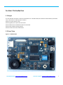
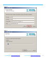
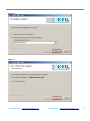
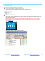
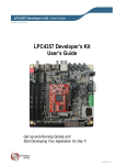
LPC4357-EVB User Manual Release:V1.1 Date 2013.01.06 Embest Info&Tech Co.,LTD. 2000-2012@ Sales &Marketing: [email protected] Technical support: [email protected] Revision History Rev Date Description 1.0 2012-11-05 Initial version 1.1 2013-01-06 Adding SDRAM, Dore Core, SD_WAV, HOST_WAV,HOST_FAT examples Modify some schematic modules Modify Quick Start part. Sales &Marketing: [email protected] Technical support: [email protected] Catalog Catalog ................................................................................................................................................................. 3 Section 1 Introduction ......................................................................................................................................... 1 1.1 Scope .................................................................................................................................................... 1 1.2 Over View ............................................................................................................................................. 1 Section 2 Quick Start ........................................................................................................................................... 2 Section 3 Evaluation Kit Hardware ...................................................................................................................... 3 3.1 Block Diagram ............................................................................................................................................ 3 3.2 Physical Size ............................................................................................................................................... 4 3.3 Electrical Parameter .................................................................................................................................. 4 3.4 ESD Precautions ......................................................................................................................................... 5 3.5 Major Functional Modules ........................................................................................................................ 5 3.5.1 Processor ............................................................................................................................................ 5 3.5.2 Memory .............................................................................................................................................. 6 3.5.3 Audio................................................................................................................................................... 8 3.5.4 USBHOST and USB Device .................................................................................................................. 9 3.5.5 SD card ................................................................................................................................................ 9 3.5.6 User keys .......................................................................................................................................... 10 3.5.7 Joystick.............................................................................................................................................. 10 3.5.8 LCD .................................................................................................................................................... 11 3.5.9 Touch Screen .................................................................................................................................... 12 3.5.10 Jumper ............................................................................................................................................ 13 Section 4 Peripherals Testing ............................................................................................................................ 14 4.1 Quick Start ............................................................................................................................................... 14 4.1.1 Preparation ....................................................................................................................................... 14 4.1.2 Running Sample ................................................................................................................................ 18 4.2 GPIO ......................................................................................................................................................... 20 4.2.1 GPIO Key ........................................................................................................................................... 20 Sales &Marketing: [email protected] Technical support: [email protected] 4.2.2 GPIO Led Blinky................................................................................................................................. 21 4.3 DUAL_CORE ............................................................................................................................................. 21 4.3.1 Int Demo ........................................................................................................................................... 21 4.3.2 Mbx Demo ........................................................................................................................................ 21 4.3.3 Queue Demo..................................................................................................................................... 22 4.4 SD card ..................................................................................................................................................... 22 4.4.1 SD_WR_RD ....................................................................................................................................... 22 4.4.2 SD_WAV............................................................................................................................................ 23 4.5 I2C-ADXL345 ............................................................................................................................................ 23 4.6 I2S ............................................................................................................................................................ 24 4.6.1 I2S warning ....................................................................................................................................... 24 4.6.2 I2S MIC .............................................................................................................................................. 25 4.6.3 I2S wav .............................................................................................................................................. 25 4.7 LCD ........................................................................................................................................................... 25 4.7.1 lcd ..................................................................................................................................................... 25 4.7.2 lcd multi ............................................................................................................................................ 26 4.8 Touchscreen ............................................................................................................................................ 26 4.9 USB .......................................................................................................................................................... 27 4.9.1 USB CDC ............................................................................................................................................ 27 4.9.2 USB HOST.......................................................................................................................................... 28 4.9.3 USB HOST FAT ................................................................................................................................... 28 4.10 SDRAM ................................................................................................................................................... 29 4.11 Mp3 Playing Demo ................................................................................................................................ 30 4.12 UcosIII demo .......................................................................................................................................... 31 4.13 emWIN display....................................................................................................................................... 31 Section 5 Purchase and service ......................................................................................................................... 32 Sales &Marketing: [email protected] Technical support: [email protected] Section 1 Introduction 1.1 Scope The User Manual introduces a functional Evaluation Kit---LPC4357-EVB, which based on NXP LPC4357 (Cortex-M4 core). The manual is made up by five sections: Section1 is scope and over view. Section2 guides you to quick start the board. Section3 describes the hardware features of the board. Section4 lists software testing projects. Section5 shows some other information. 1.2 Over View Figure 1-1 LPC4357-EVB Sales &Marketing: [email protected] Technical support: [email protected] 1 Section 2 Quick Start You can refer to the----- Quick Start Guide for LPC4357-EVB. Sales &Marketing: [email protected] Technical support: [email protected] 2 Section 3 Evaluation Kit Hardware 3.1 Block Diagram Figure 3-1 LPC4357-EVB Block Diagram Sales &Marketing: [email protected] Technical support: [email protected] 3 3.2 Physical Size Figure 3-2 front size 3.3 Electrical Parameter Supply Voltage: 5 Volts DC (Provided by power adapter) Supply Current: 0.5A Temperature: 0~70℃ Micro Controller: LPC4357, 256 pin BGA Board Size: 105cm*75cm Weight: 50g Peripherals: (1) LCD interface for a QVGA LCD module (sold as an optional accessory) (2) Audio codec and audio jacks (3) Two USB ports, one HS (High speed USB host) port and one FS (Full Speed device) port (4) 3 axis accelerometer from Analog Devices (5) Five user input switches (6) Joystick (Five way switch) Sales &Marketing: [email protected] Technical support: [email protected] 4 (7) One user LED (8) One ISP switch and one reset switch (9) Boot select switch (10) Crystals for controller, RTC and audio codec (11) On board USB host power switch (12) 20-pin Cortex debug header 3.4 ESD Precautions Please note that the LPC4357-EVB board and K430WQA-V5-F LCD come without any casing/box. All components are exposed. Therefore, extra attention must be paid to ESD (electrostatic discharge) Precautions. To make sure that there is no static interference when using this board. Appropriate ESD protections must be taken and wearing electrostatic equipment is recommended, such as wearing an anti-static wristband. ESD damage can range from subtle performance degradation to complete device failure. Precision integrated circuits may be more susceptible to damage because of very small parametric changes could cause the device not meet its published specifications. Warning: This is a class A product, in a domestic this product may cause radio interference in which case users may be required to take adequate measures. 3.5 Major Functional Modules 3.5.1 Processor The LPC43xx are ARM Cortex-M4 based microcontrollers for embedded applications which include an ARM Cortex-M0 coprocessor, up to 1 MB of flash, up to 264 KB of SRAM, advanced configurable peripherals such as the State Configurable Timer (SCT)and the Serial General Purpose I/O (SGPIO) interface, two High-speed USB controllers, Ethernet, LCD, an external memory controller, and multiple digital and analog peripherals. The LPC43xx operate at CPU frequencies of up to 204 MHZ. The ARM Cortex-M4 is a next generation 32-bit core that offers system enhancements such as low power consumption, enhanced debug features, and a high level of support block integration. The ARM Cortex-M4 CPU incorporates a 3-stage pipeline, uses a Harvard architecture with separate local instruction and data buses as well as a third bus for peripherals, and includes an internal pre fetch unit that supports speculative branching. The ARM Cortex-M4 supports single-cycle digital signal processing and SIMD instructions. A hardware floating-point processor is integrated in the core. The ARM Cortex-M0 coprocessor is an energy-efficient and easy-to-use 32-bit core which is code- and tool-compatible with the Cortex-M4 core. The Cortex-M0 coprocessor, designed as a replacement for existing 8/16-bit microcontrollers, offers up to 204 MHz performance with a simple instruction set and reduced code size. More feature detail you can refer to NXP official site: http://www.nxp.com/documents/user_manual/UM10503.pdf Sales &Marketing: [email protected] Technical support: [email protected] 5 3.5.2 Memory The LPC4357 processor features an external memory controller and SPI Flash Interface (SPIFI). Two kinds of memory devices are connected: One 256Mbits SDRAM, using EMC. One 256Mbits SPI Flash performs through SPIFI. Sales &Marketing: [email protected] Technical support: [email protected] 6 Figure3-3 SDRAM module Figure3-4 SPIflash module Sales &Marketing: [email protected] Technical support: [email protected] 7 3.5.3 Audio The processor is configured in IIS mode to interface with the stereo audio coder-decode ---UDA1380. Sound can be input through audio in (J5),output by headphone out (J6) or Speaker(SP1). Figure3-5 Sales &Marketing: [email protected] Technical support: [email protected] 8 3.5.4 USBHOST and USB Device USB0 can be configured as USB0 Host/Device/OTG mode, and the USB1 can be Host/Device. Figure3-6 3.5.5 SD card Figure3-7 Sales &Marketing: [email protected] Technical support: [email protected] 9 3.5.6 User keys The board offers five user keys, controlled by GPIOs. Figure3-8 3.5.7 Joystick The kit equips a Joystick, controlled by GPIOs. Figure3-9 Sales &Marketing: [email protected] Technical support: [email protected] 10 3.5.8 LCD A 4’ 480*272 LCD is optional module. Here we offer its hardware interface. Figure3-10 Sales &Marketing: [email protected] Technical support: [email protected] 11 3.5.9 Touch Screen Touch Screen control module. Figure3-11 Sales &Marketing: [email protected] Technical support: [email protected] 12 3.5.10 Jumper Figure 3-12 Jumpers (USB0 Boot Mode Shown) Table 3-1 Boot mode jumper settings Boot mode 1 2 3 4 Description USART0 UP UP UP UP Boot from device connected to USART0 using pins P2_0 and P2_1. For flash parts, enter UART ISP mode. SPIFI DN UP UP UP Boot from Quad SPI flash connected to the SPIFI interface on P3_3 to P3_8 EMC 8-bit UP DN UP UP Boot from external static memory (such as NOR flash) using CS0 and an 8-bit data bus. EMC 16-bit DN DN UP UP Boot from external static memory (such as NOR flash) using CS0 and a 16-bit data bus. EMC 32-bit UP UP DN UP Boot from external static memory (such as NOR flash) using CS0 and a 32-bit data bus. USB0 USB1 SPI(SSP) DN UP DN UP DN DN DN DN DN UP UP UP Boot from USB0. Boot from USB1. Boot from SPI flash connected to the SSP0 interface on P3_3 (function SSP0_SCK), P3_6 (function SSP0_MISO), P3_7 (function SSP0_MOSI), and P3_8 (function SSP0_SSEL). USART3 DP DP DP DN Boot from device connected to USART3 using pins P2_3 and P2_4. For flash parts, enter UART ISP mode. Sales &Marketing: [email protected] Technical support: [email protected] 13 Section 4 Peripherals Testing We offer relevant software to realize its hardware function. All the projects are running in keil-MDK4.60. 4.1 Quick Start 4.1.1 Preparation Need a debugger. Here we use ULink2. Recommended PC system configuration as below: 2.0GHz (or higher) of the CPU 512M RAM USB interfaces A serial interface Windows XP operating system KEIL4.60 Integrated Development Environment installed. The following steps teach you how to install it. Figure 2-1 Sales &Marketing: [email protected] Technical support: [email protected] 14 Figure 2-2 Figure 2-3 Sales &Marketing: [email protected] Technical support: [email protected] 15 Figure 2-4 Figure 2-5 Sales &Marketing: [email protected] Technical support: [email protected] 16 Figure 2-6 Figure 2-7 Sales &Marketing: [email protected] Technical support: [email protected] 17 4.1.2 Running Sample Here we choose a simple LED_Blinky as the running demo. First we need to double click to open the project. (route: LPC4357-EVB\Examples\01-GPIO\Gpio_LedBlinky\Keil\Gpio_LedBlinky.uvproj) Secondly we build the project. Here we offer 3 kinds of configuration for download or debug: Inflash, SPIflash and InterSRAM. And we use Inflash to show the example. Note: INflash boot is prior to any other outside booting (including SPIFLASH boot). So you must erase the INflash memory if you want to use SPI flash boot, and set the jumpers as below. Other boot settings please refer to chapter3.5.10. Choose Inflash module, and click the “bulid (F7)” button. Successfully build. Sales &Marketing: [email protected] Technical support: [email protected] 18 Download. After building, we download image to the board. Click the download button, and waiting. Successfully download as below: Running Reset the board. You can see the LED D6 is blinking. Debug You can also choose to debug the example. You just need to click the debug button after building the example. As below: Sales &Marketing: [email protected] Technical support: [email protected] 19 Quick start module is over, and you can try the below examples. Note: the SD card and U Stick storage, they’re both no more than 2GB. 4.2 GPIO Location: LPC4357-EVB\Examples\01-GPIO 4.2.1 GPIO Key The project describes how to use keys through GPIO controller. Preparation: (1) Power support: power line (J8) connection. (2) JTAG Debugger Connection:One end is connected to JTAG interface on the board (J9), the other to PC. (3) Turn on the switch (SW2). (4) Build the project, and download the image to the board, as chapter 4.1.2. Phenomenon: Reset the board. Press any key(K1~K5 or joystick), the LED D6 is on, and out if you release. Sales &Marketing: [email protected] Technical support: [email protected] 20 4.2.2 GPIO Led Blinky The project describes how to use LEDs through GPIO controller. Preparation: (1) Power support: power line (J8) connection. (2) JTAG Debugger Connection:One end is connected to JTAG interface on the board (J9), the other to PC. (3) Turn on the switch (SW2). (4) Build the project, and download the image to the board, as chapter 4.1.2. Phenomenon: Reset the board. The LED D6 is blinking. 4.3 DUAL_CORE Location: LPC4357-EVB\Examples\03-DUAL_CORE 4.3.1 Int Demo The project describes how the dual cores communicate through interruption. Preparation: (1) Power support: power line (J8) connection. (2) JTAG Debugger Connection:One end is connected to JTAG interface on the board (J9), the other to PC. (3) Turn on the switch (SW2). (4) Build the project, and download the image to the board, as chapter 4.1.2. Note: first build M0 image, and then M4. After building, download M4 image into the board. Phenomenon: Reset the board. The LED D6 is blinking. 4.3.2 Mbx Demo The project describes how the dual cores communicate through mailbox function. Preparation: (1) Power support: power line (J8) connection. (2) Headphone connection: use a earphone to connect the board (J6). (3) U Stick: prepare a U stick (4) WAV File: copy the psy.wav to your U Stick root directory. (You can also use your own .wav file, but you should rename it as psy.wav) (5) JTAG Debugger Connection:One end is connected to JTAG interface on the board (J9), the other to PC. (6) Turn on the switch (SW2). (7) Build the project, and download the image to the board, as chapter 4.1.2. Note: first build M0 image, and then M4. After building, download M4 image into the board. Phenomenon: Reset the board. Then insert the U Stick, and you can hear the music from either the speaker or the headphone. Sales &Marketing: [email protected] Technical support: [email protected] 21 4.3.3 Queue Demo The project describes how the dual cores communicate through mailbox function. Preparation: (1) Power support: power line (J8) connection. (2) Headphone connection: use a earphone to connect the board (J6). (3) U Stick: prepare a U stick. (4) WAV File: copy the psy.wav to your U Stick root directory. (You can also use your own .wav file, but you should rename it as psy.wav) (5) JTAG Debugger Connection:One end is connected to JTAG interface on the board (J9), the other to PC. (6) Turn on the switch (SW2). (7) Build the project, and download the image to the board, as chapter 4.1.2. Note: First build M0 image, and then M4. After building, download both M0 and M4 image into the board. Phenomenon: Reset the board. Then insert the U Stick, and you can hear the music from either the speaker or the headphone. 4.4 SD card Location: LPC4357-EVB\Examples\04-SDcard 4.4.1 SD_WR_RD The project describes how to read and write the SD card. Preparation: (1) Power support: power line (J8) connection. (2) USB device connection: connect the board to the computer through the USB device interface (J7). (3) SD card connection: put a SD card in the SD card interface (J10). (4) JTAG Debugger Connection: One end is connected to JTAG interface on the board (J9), the other to PC . (5) Turn on the switch (SW2). (6) Build the project, and download the image to the board, as chapter 4.1.2. Phenomenon: Reset the board. After the PC realize the virtual COM, open your terminal, configured as below: Baud rate: 9600 Data bit: 8bits Stop bit: 1bit Check bit: none Data flow control: none Press K1, terminal will show the information as below: SD card demo is runing. the number we write in is : a the number we read from is: a the number we write in is : a Sales &Marketing: [email protected] Technical support: [email protected] 22 the number we read from is: a …… ….. … the number we write in is : a the number we read from is: a the number we write in is : a the number we read from is: a Verify success! 4.4.2 SD_WAV The project describes how to play WAV file in the SDcard. Preparation: (1) Power support: power line (J8) connection. (2) USB device connection: connect the board to the computer through the USB device interface (J7). (3) WAV file: copy the aaa.wav to your SD card root directory. (You can also use your own .wav file, but you should rename it as aaa.wav) (4) SD card connection: put the SD card in the SD card interface (J10). (5) Earphone connection: connect your earphone to the board through the headphone interface (J6). (6) JTAG Debugger Connection: One end is connected to JTAG interface on the board (J9), the other to PC . (7) Turn on the switch (SW2). (8) Build the project, and download the image to the board, as chapter 4.1.2. Phenomenon: Reset the board and you can hear the aaa.wav playing from your earphone. 4.5 I2C-ADXL345 Location: LPC4357-EVB\Examples\05-I2C_ADXL345 The project describes how to read coordinate on the ADXL345 registers. Preparation: (1) Power support: power line (J8) connection. (2) USB device connection: connect the board to the computer through the USB device interface (J7). (3) JTAG Debugger Connection: One end is connected to JTAG interface on the board (J9), the other to PC . (4) Turn on the switch (SW2). (5) Build the project, and download the image to the board, as chapter 4.1.2. Phenomenon: Reset the board. After the PC realize the virtual COM, open your terminal, configured as below: Baud rate: 9600 Data bit: 8bits Sales &Marketing: [email protected] Technical support: [email protected] 23 Stop bit: 1bit Check bit: none Data flow control: none Shake the board, terminal will show the coordinate information as below: 4.6 I2S Location: LPC4357-EVB\Examples\06-I2S 4.6.1 I2S warning The project describes how to use I2S controller to play audio files. Preparation: (1) Power support: power line (J8) connection. (2) Headphone connection: use a earphone to connect the board (J6). (3) JTAG Debugger Connection:One end is connected to JTAG interface on the board (J9), the other to PC. (4) Turn on the switch (SW2). (5) Build the project, and download the image to the board, as chapter 4.1.2. Phenomenon: Reset the board. You can hear the warning sound from either the speaker or the headphone. Sales &Marketing: [email protected] Technical support: [email protected] 24 4.6.2 I2S MIC The project describes how to use I2S controller to play audio files. Preparation: (1) Power support: power line (J8) connection. (2) Headphone connection: use a earphone to connect the board (J6), and connect its microphone with the board through J5. (3) JTAG Debugger Connection:One end is connected to JTAG interface on the board (J9), the other to PC. (4) Turn on the switch (SW2). (5) Build the project, and download the image to the board, as chapter 4.1.2. Phenomenon: Reset the board. First you can hear a piece of soft music from the headphone and after that you can speak loudly to the microphone, then you’ll hear what you say from the earphone. 4.6.3 I2S wav The project describes how to use I2S controller to play audio files. Preparation: (8) Power support: power line (J8) connection. (9) Headphone connection: use a earphone to connect the board (J6). (10) U Stick: prepare a U stick (11) WAV File: copy the psy.wav to your U Stick root directory. (You can also use your own .wav file, but you should rename it as psy.wav) (12) JTAG Debugger Connection:One end is connected to JTAG interface on the board (J9), the other to PC. (13) Turn on the switch (SW2). (14) Build the project, and download the image to the board, as chapter 4.1.2. Phenomenon: Reset the board. Then insert the U Stick, and you can hear the music from either the speaker or the headphone. 4.7 LCD Location: LPC4357-EVB\Examples\07-LCD 4.7.1 lcd The project describes the LCD display. Preparation: (1) Power support: power line (J8) connection. (2) LCD connection: connect the optional LCD to the board. (3) JTAG Debugger Connection:One end is connected to JTAG interface on the board (J9), the other to PC. (4) Turn on the switch (SW2). (5) Build the project, and download the image to the board, as chapter 4.1.2. Phenomenon: Reset the board. You can see a picture displayed. Sales &Marketing: [email protected] Technical support: [email protected] 25 4.7.2 lcd multi The project describes the LCD play two pictures. Preparation: (1) Power support: power line (J8) connection. (2) LCD connection: connect the optional LCD to the board. (3) JTAG Debugger Connection:One end is connected to JTAG interface on the board (J9), the other to PC. (4) Turn on the switch (SW2). (5) Build the project, and download the image to the board, as chapter 4.1.2. Phenomenon: Reset the board. You can see two beautiful pictures displaying. 4.8 Touch screen Location: LPC4357-EVB\Examples\08-Touch_Screen The project test the touchscreen Preparation: (1) Power support: USB device (J7) or power line (J8) connection. (2) LCD connection: connect the optional LCD to the board. (3) JTAG Debugger Connection: One end is connected to JTAG interface on the board (J9), the other to PC. (4) Turn on the switch (SW2) if you choose the power line support. (5) Build the project, and download the image to the board, as chapter 4.1.2. Phenomenon: Reset the board. PC will inform you to install a driver. Do as it request. The .inf file (lpc18xx-vcom) lies here: When you’ve installed it, the virtual COM will show in your device manager. Then open your terminal, configured as below: Baud rate: 115200 Data bit: 8bits Stop bit: 1bit Check bit: none Data flow control: none Press K1, and insert the U stick again. The terminal will show the touch coordinate information as below: The x value 3749 The y value 3480 The z value 201 The x value 3789 The y value 335 The z value 217 The x value 355 The y value 3349 The z value 58 The x value 213 The y value 356 The z value 212 Sales &Marketing: [email protected] Technical support: [email protected] 26 4.9 USB Location: LPC4357-EVB\Examples\09-USB 4.9.1 USB CDC The project describes how to make USB device as a virtual COM, working as a serial port. Preparation: (1) Power support: power line (J8) connection. (2) USB device connection: connect the board to the computer through the USB device interface (J7). (3) JTAG Debugger Connection:One end is connected to JTAG interface on the board (J9), the other to PC. (4) Turn on the switch (SW2). (5) Build the project, and download the image to the board, as chapter 4.1.2. Phenomenon: Reset the board. After the PC realize the virtual COM, open your terminal, configured as below: Baud rate: 9600 Data bit: 8bits Stop bit: 1bit Check bit: none Data flow control: none Press key K1~K5, terminal will show the information as below: Sales &Marketing: [email protected] Technical support: [email protected] 27 4.9.2 USB HOST The project describes how to read and write the U stick Preparation: (1) Power support: power line (J8) connection. (2) USB device connection: connect the board to the computer through the USB device interface (J7). (3) JTAG Debugger Connection: One end is connected to JTAG interface on the board (J9), the other to PC . (4) Turn on the switch (SW2). (5) U Stick: prepare a U stick. (6) Turn on the switch. (7) Build the project, and download the image to the board, as chapter 4.1.2. Phenomenon: Reset the board. After the PC realize the virtual COM, open your terminal, configured as below: Baud rate: 9600 Data bit: 8bits Stop bit: 1bit Check bit: none Data flow control: none Insert the U stick to the USB Host interface (J4). The terminal will show the information as below: 4.9.3 USB HOST FAT The project describes how to read and write the U stick Preparation: (1) Power support: power line (J8) connection. (2) USB device connection: connect the board to the computer through the USB device interface (J7). Sales &Marketing: [email protected] Technical support: [email protected] 28 (3) JTAG Debugger Connection: One end is connected to JTAG interface on the board (J9), the other to PC . (4) Turn on the switch (SW2). (5) U Stick: prepare a U stick. (6) Turn on the switch. (7) Build the project, and download the image to the board, as chapter 4.1.2. Phenomenon: (1) Create a .txt file, named 1. You can write anything in this file, save it and put it in the U Stick. Here I write as below: (2) Reset the board. After the PC realize the virtual COM, open your terminal, configured as below: Baud rate: 9600 Data bit: 8bits Stop bit: 1bit Check bit: none Data flow control: none Insert the U stick to the USB Host interface (J4). The terminal will show what you’ve written in the 1.txt file, as below: 4.10 SDRAM Location: LPC4357-EVB\Examples\02-SDRAM The project describes how to read and write the SD card. Preparation: (1) Power support: power line (J8) connection. (2) USB device connection: connect the board to the computer through the USB device interface (J7). (3) JTAG Debugger Connection: One end is connected to JTAG interface on the board (J9), the other to PC . (4) Turn on the switch (SW2). Sales &Marketing: [email protected] Technical support: [email protected] 29 (5) Build the project, and download the image to the board, as chapter 4.1.2. Phenomenon: Reset the board. After the PC realize the virtual COM, open your terminal, configured as below: Baud rate: 9600 Data bit: 8bits Stop bit: 1bit Check bit: none Data flow control: none The terminal will show the check information as below: 4.11 Mp3 Playing Demo Location: LPC4357-EVB\Examples\MP3Demo_dualcore The demo is a comprehensive application of the board. It features as: emWin graphics library Cortex-M4 for audio decoding and playing Cortex-M0 for HS USB and data transfer from USB stic Touchscreen controls playing list. Preparation: (1) Power support: power line (J8) connection. (2) LCD connection: connect the optional LCD to the board. (3) U Stick: download mp3 songs into the U stick, and insert it to the board (J4). (4) Headphone connection: use a earphone to connect the board (J6). (5) JTAG Debugger Connection:One end is connected to JTAG interface on the board (J9), the other to PC. (6) Turn on the switch (SW2). Sales &Marketing: [email protected] Technical support: [email protected] 30 (7) Build the project, and download the image to the board, as chapter 4.1.2. Phenomenon: Reset the board. Press playing button in the LCD, and you can hear the music playing. You can see the playing list and choose playing pre or next, start or pause. 4.12 UcosIII demo Location: LPC4357-EVB\ucos-III The project shows a basic function of ucosIII, version3.02. Preparation: (1) Power support: power line (J8) connection. (2) JTAG Debugger Connection: One end is connected to JTAG interface on the board (J9), the other to PC . (3) Turn on the switch (SW2). (4) Build the project, and download the image to the board, as chapter 4.1.2. Phenomenon: Reset the board. You can see the D6 is shining. One task makes it on, and another makes it down. 4.13 emWIN display Location: LPC4357-EVB\Examples\emWin_GUIDemo The project describes the emWIN function. Preparation: (1) Power support: power line (J8) connection. (2) LCD connection: connect the optional LCD to the board. (3) JTAG Debugger Connection:One end is connected to JTAG interface on the board (J9), the other to PC. (4) Turn on the switch (SW2). (5) Build the project, and download the image to the board, as chapter 4.1.2. Phenomenon: Reset the board. You can see dynamic pictures displayed. Sales &Marketing: [email protected] Technical support: [email protected] 31 Section 5 Purchase and service If you are interested in the board, you may connect: Sales and marketing: [email protected] For Technical Support: [email protected] URL: http://www.embedinfo.com/en/ HU U HU HU U U Sales &Marketing: [email protected] Technical support: [email protected] 32