1
CX29704
OptiPHY-F155 STS-3/STM-1 SONET/SDH ATM/POS Framer
EVM User Manual
29704-EVMD-001-C
June 2005
CX29704 EVM User Manual
OptiPHY-F155 STS-3/STM-1 SONET/SDH ATM/POS Framer
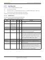
Revision History
Revision
Level
Date
C
Released
June 2005
B
Advance
November 2004
Description
Updated document number.
First revision for external use.
© 2005, Mindspeed TechnologiesTM, Inc. All rights reserved.
Information in this document is provided in connection with Mindspeed TechnologiesTM ("MindspeedTM") products.
These materials are provided by Mindspeed as a service to its customers and may be used for informational
purposes only. Except as provided in Mindspeed’s Terms and Conditions of Sale for such products or in any
separate agreement related to this document, Mindspeed assumes no liability whatsoever. Mindspeed assumes no
responsibility for errors or omissions in these materials. Mindspeed may make changes to specifications and
product descriptions at any time, without notice. Mindspeed makes no commitment to update the information and
shall have no responsibility whatsoever for conflicts or incompatibilities arising from future changes to its
specifications and product descriptions. No license, express or implied, by estoppel or otherwise, to any intellectual
property rights is granted by this document.
THESE MATERIALS ARE PROVIDED "AS IS" WITHOUT WARRANTY OF ANY KIND, EITHER EXPRESS OR
IMPLIED, RELATING TO SALE AND/OR USE OF MINDSPEED PRODUCTS INCLUDING LIABILITY OR
WARRANTIES RELATING TO FITNESS FOR A PARTICULAR PURPOSE, CONSEQUENTIAL OR INCIDENTAL
DAMAGES, MERCHANTABILITY, OR INFRINGEMENT OF ANY PATENT, COPYRIGHT OR OTHER
INTELLECTUAL PROPERTY RIGHT. MINDSPEED FURTHER DOES NOT WARRANT THE ACCURACY OR
COMPLETENESS OF THE INFORMATION, TEXT, GRAPHICS OR OTHER ITEMS CONTAINED WITHIN THESE
MATERIALS. MINDSPEED SHALL NOT BE LIABLE FOR ANY SPECIAL, INDIRECT, INCIDENTAL, OR
CONSEQUENTIAL DAMAGES, INCLUDING WITHOUT LIMITATION, LOST REVENUES OR LOST PROFITS,
WHICH MAY RESULT FROM THE USE OF THESE MATERIALS.
Mindspeed products are not intended for use in medical, lifesaving or life sustaining applications. Mindspeed
customers using or selling Mindspeed products for use in such applications do so at their own risk and agree to
fully indemnify Mindspeed for any damages resulting from such improper use or sale.
www.mindspeed.com
General Information:
(949) 579-3000
Headquarters - Newport Beach
4000 MacArthur Blvd., East Tower
Newport Beach, CA. 92660
29704-EVMD-001-C
Mindspeed Technologies™
Mindspeed Proprietary and Confidential
Table of Contents
Revision History . . . . . . . . . . . . . . . . . . . . . . . . . . . . . . . . . . . . . . . . . . . . . . . . . . . . . ii
1.0 Getting Started . . . . . . . . . . . . . . . . . . . . . . . . . . . . . . . . . . . . . . . . . . . . . . . . . . . . . . 1
1.1
Introduction . . . . . . . . . . . . . . . . . . . . . . . . . . . . . . . . . . . . . . . . . . . . . . . . . . . . . . . . . . . . . . 1
1.1.1
1.1.2
System Overview . . . . . . . . . . . . . . . . . . . . . . . . . . . . . . . . . . . . . . . . . . . . . . . . . . . . . . . . . . . . . . 1
Hardware Overview . . . . . . . . . . . . . . . . . . . . . . . . . . . . . . . . . . . . . . . . . . . . . . . . . . . . . . . . . . . . 2
1.1.2.1 EVM Top View . . . . . . . . . . . . . . . . . . . . . . . . . . . . . . . . . . . . . . . . . . . . . . . . . . . . . . . . . . . . . .3
1.1.3
Software Architecture . . . . . . . . . . . . . . . . . . . . . . . . . . . . . . . . . . . . . . . . . . . . . . . . . . . . . . . . . . . 4
1.1.3.1 EVM Software Graphical User Interface (GUI) . . . . . . . . . . . . . . . . . . . . . . . . . . . . . . . . . . . . . .4
1.1.4
Reference Documents . . . . . . . . . . . . . . . . . . . . . . . . . . . . . . . . . . . . . . . . . . . . . . . . . . . . . . . . . . 4
1.1.4.1 Mindspeed Technologies Documents . . . . . . . . . . . . . . . . . . . . . . . . . . . . . . . . . . . . . . . . . . . .4
1.2
1.3
1.4
Unpacking . . . . . . . . . . . . . . . . . . . . . . . . . . . . . . . . . . . . . . . . . . . . . . . . . . . . . . . . . . . . . . . 5
Requirements . . . . . . . . . . . . . . . . . . . . . . . . . . . . . . . . . . . . . . . . . . . . . . . . . . . . . . . . . . . . 5
Installation Procedures . . . . . . . . . . . . . . . . . . . . . . . . . . . . . . . . . . . . . . . . . . . . . . . . . . . . . 5
1.4.1
Hardware Assembly . . . . . . . . . . . . . . . . . . . . . . . . . . . . . . . . . . . . . . . . . . . . . . . . . . . . . . . . . . . . 5
1.4.1.1 Handling . . . . . . . . . . . . . . . . . . . . . . . . . . . . . . . . . . . . . . . . . . . . . . . . . . . . . . . . . . . . . . . . . .5
1.4.1.2 Board Assembly . . . . . . . . . . . . . . . . . . . . . . . . . . . . . . . . . . . . . . . . . . . . . . . . . . . . . . . . . . . .5
1.4.1.3 Flash Memory . . . . . . . . . . . . . . . . . . . . . . . . . . . . . . . . . . . . . . . . . . . . . . . . . . . . . . . . . . . . . .5
1.4.2
1.4.3
1.5
Setting the IP Address . . . . . . . . . . . . . . . . . . . . . . . . . . . . . . . . . . . . . . . . . . . . . . . . . . . . . . . . . . 6
Installing the EVM GUI software . . . . . . . . . . . . . . . . . . . . . . . . . . . . . . . . . . . . . . . . . . . . . . . . . . 7
Quick Start Procedure . . . . . . . . . . . . . . . . . . . . . . . . . . . . . . . . . . . . . . . . . . . . . . . . . . . . . . 8
1.5.1
1.5.2
Running the software . . . . . . . . . . . . . . . . . . . . . . . . . . . . . . . . . . . . . . . . . . . . . . . . . . . . . . . . . . . 8
Startup Screen and loading a data file . . . . . . . . . . . . . . . . . . . . . . . . . . . . . . . . . . . . . . . . . . . . . . 8
1.5.2.1 New EVM file . . . . . . . . . . . . . . . . . . . . . . . . . . . . . . . . . . . . . . . . . . . . . . . . . . . . . . . . . . . . . . .9
1.5.2.2 Existing EVM File . . . . . . . . . . . . . . . . . . . . . . . . . . . . . . . . . . . . . . . . . . . . . . . . . . . . . . . . . . .10
2.0 GUI Operation . . . . . . . . . . . . . . . . . . . . . . . . . . . . . . . . . . . . . . . . . . . . . . . . . . . . . . 11
2.1
Jump Start Screen . . . . . . . . . . . . . . . . . . . . . . . . . . . . . . . . . . . . . . . . . . . . . . . . . . . . . . . . 11
2.1.1
2.1.2
2.1.3
2.1.4
2.1.5
2.1.6
2.2
13
13
13
14
14
14
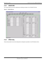
CX29704 Registers Screen . . . . . . . . . . . . . . . . . . . . . . . . . . . . . . . . . . . . . . . . . . . . . . . . . 15
2.2.1
2.2.2
2.2.3
2.3
2.4
Payload Contents . . . . . . . . . . . . . . . . . . . . . . . . . . . . . . . . . . . . . . . . . . . . . . . . . . . . . . . . . . . . .
Framing Format . . . . . . . . . . . . . . . . . . . . . . . . . . . . . . . . . . . . . . . . . . . . . . . . . . . . . . . . . . . . . .
Timing Source . . . . . . . . . . . . . . . . . . . . . . . . . . . . . . . . . . . . . . . . . . . . . . . . . . . . . . . . . . . . . . .
Loopback . . . . . . . . . . . . . . . . . . . . . . . . . . . . . . . . . . . . . . . . . . . . . . . . . . . . . . . . . . . . . . . . . . .
Packet/ATM FPGA Mode . . . . . . . . . . . . . . . . . . . . . . . . . . . . . . . . . . . . . . . . . . . . . . . . . . . . . . .
Log Pane . . . . . . . . . . . . . . . . . . . . . . . . . . . . . . . . . . . . . . . . . . . . . . . . . . . . . . . . . . . . . . . . . . .
Reading a register . . . . . . . . . . . . . . . . . . . . . . . . . . . . . . . . . . . . . . . . . . . . . . . . . . . . . . . . . . . . 15
Writing a register . . . . . . . . . . . . . . . . . . . . . . . . . . . . . . . . . . . . . . . . . . . . . . . . . . . . . . . . . . . . . 16
Update command . . . . . . . . . . . . . . . . . . . . . . . . . . . . . . . . . . . . . . . . . . . . . . . . . . . . . . . . . . . . . 16
Packet/ATM FPGA Registers Screen . . . . . . . . . . . . . . . . . . . . . . . . . . . . . . . . . . . . . . . . . . 16
OH FPGA Registers Screen . . . . . . . . . . . . . . . . . . . . . . . . . . . . . . . . . . . . . . . . . . . . . . . . . 16
29704-EVMD-001-C
Mindspeed Technologies™
Mindspeed Proprietary and Confidential
iii
CX29704 EVM User Manual
2.5
OptiPHY-F155 STS-3/STM-1 SONET/SDH ATM/POS Framer
TAP Driver Parameter Screens . . . . . . . . . . . . . . . . . . . . . . . . . . . . . . . . . . . . . . . . . . . . . . . 16
2.5.1
2.5.2
2.5.3
2.5.4
CX29704 Config . . . . . . . . . . . . . . . . . . . . . . . . . . . . . . . . . . . . . . . . . . . . . . . . . . . . . . . . . . . . . .
CX29704 FM . . . . . . . . . . . . . . . . . . . . . . . . . . . . . . . . . . . . . . . . . . . . . . . . . . . . . . . . . . . . . . . .
CX29704 PM . . . . . . . . . . . . . . . . . . . . . . . . . . . . . . . . . . . . . . . . . . . . . . . . . . . . . . . . . . . . . . . .
FPGA Config . . . . . . . . . . . . . . . . . . . . . . . . . . . . . . . . . . . . . . . . . . . . . . . . . . . . . . . . . . . . . . . . .
17
18
19
19
3.0 Software Description . . . . . . . . . . . . . . . . . . . . . . . . . . . . . . . . . . . . . . . . . . . . . . . . 20
3.1
3.2
Software Architecture . . . . . . . . . . . . . . . . . . . . . . . . . . . . . . . . . . . . . . . . . . . . . . . . . . . . . 20
EVM Software . . . . . . . . . . . . . . . . . . . . . . . . . . . . . . . . . . . . . . . . . . . . . . . . . . . . . . . . . . . 21
3.2.1
3.2.2
3.2.3
3.2.4
3.2.5
3.3
RTOS . . . . . . . . . . . . . . . . . . . . . . . . . . . . . . . . . . . . . . . . . . . . . . . . . . . . . . . . . . . . . . . . . . . . . .
Communications . . . . . . . . . . . . . . . . . . . . . . . . . . . . . . . . . . . . . . . . . . . . . . . . . . . . . . . . . . . . .
CX29704 TAP . . . . . . . . . . . . . . . . . . . . . . . . . . . . . . . . . . . . . . . . . . . . . . . . . . . . . . . . . . . . . . . .
FPGA Device Driver . . . . . . . . . . . . . . . . . . . . . . . . . . . . . . . . . . . . . . . . . . . . . . . . . . . . . . . . . . .
EVM Application Code . . . . . . . . . . . . . . . . . . . . . . . . . . . . . . . . . . . . . . . . . . . . . . . . . . . . . . . . .
21
21
21
21
21
Host Software . . . . . . . . . . . . . . . . . . . . . . . . . . . . . . . . . . . . . . . . . . . . . . . . . . . . . . . . . . . 22
3.3.1
3.3.2
Communications Protocol . . . . . . . . . . . . . . . . . . . . . . . . . . . . . . . . . . . . . . . . . . . . . . . . . . . . . . 22
Graphical User Interface (GUI) . . . . . . . . . . . . . . . . . . . . . . . . . . . . . . . . . . . . . . . . . . . . . . . . . . . 22
4.0 Hardware Description . . . . . . . . . . . . . . . . . . . . . . . . . . . . . . . . . . . . . . . . . . . . . . . . 23
4.1
Hardware Architecture . . . . . . . . . . . . . . . . . . . . . . . . . . . . . . . . . . . . . . . . . . . . . . . . . . . . . 23
4.1.1
4.1.2
4.1.3
4.1.4
CX29704 . . . . . . . . . . . . . . . . . . . . . . . . . . . . . . . . . . . . . . . . . . . . . . . . . . . . . . . . . . . . . . . . . . .
Packet/ATM FPGA . . . . . . . . . . . . . . . . . . . . . . . . . . . . . . . . . . . . . . . . . . . . . . . . . . . . . . . . . . . .
Overhead FPGA . . . . . . . . . . . . . . . . . . . . . . . . . . . . . . . . . . . . . . . . . . . . . . . . . . . . . . . . . . . . . .
Control Subsystem . . . . . . . . . . . . . . . . . . . . . . . . . . . . . . . . . . . . . . . . . . . . . . . . . . . . . . . . . . . .
25
25
25
25
4.1.4.1 Internal Memory Map . . . . . . . . . . . . . . . . . . . . . . . . . . . . . . . . . . . . . . . . . . . . . . . . . . . . . . .26
4.1.5
4.1.6
Oscillators . . . . . . . . . . . . . . . . . . . . . . . . . . . . . . . . . . . . . . . . . . . . . . . . . . . . . . . . . . . . . . . . . . 26
Power . . . . . . . . . . . . . . . . . . . . . . . . . . . . . . . . . . . . . . . . . . . . . . . . . . . . . . . . . . . . . . . . . . . . . . 26
4.1.6.1 External Power . . . . . . . . . . . . . . . . . . . . . . . . . . . . . . . . . . . . . . . . . . . . . . . . . . . . . . . . . . . .26
4.1.6.2 EVM Regulators . . . . . . . . . . . . . . . . . . . . . . . . . . . . . . . . . . . . . . . . . . . . . . . . . . . . . . . . . . . .26
4.2
Line-Side Interface . . . . . . . . . . . . . . . . . . . . . . . . . . . . . . . . . . . . . . . . . . . . . . . . . . . . . . . . 27
4.2.1
4.3
Electrical Interfaces . . . . . . . . . . . . . . . . . . . . . . . . . . . . . . . . . . . . . . . . . . . . . . . . . . . . . . . 27
4.3.1
4.3.2
4.3.3
4.3.4
4.3.5
4.4
Optical Front-End . . . . . . . . . . . . . . . . . . . . . . . . . . . . . . . . . . . . . . . . . . . . . . . . . . . . . . . . . . . . . 27
Signal Description . . . . . . . . . . . . . . . . . . . . . . . . . . . . . . . . . . . . . . . . . . . . . . . . . . . . . . . . . . . .
JTAG . . . . . . . . . . . . . . . . . . . . . . . . . . . . . . . . . . . . . . . . . . . . . . . . . . . . . . . . . . . . . . . . . . . . . .
Test Points . . . . . . . . . . . . . . . . . . . . . . . . . . . . . . . . . . . . . . . . . . . . . . . . . . . . . . . . . . . . . . . . . .
UL2 Connectors . . . . . . . . . . . . . . . . . . . . . . . . . . . . . . . . . . . . . . . . . . . . . . . . . . . . . . . . . . . . . .
Power Interface . . . . . . . . . . . . . . . . . . . . . . . . . . . . . . . . . . . . . . . . . . . . . . . . . . . . . . . . . . . . . .
27
27
28
28
28
Other Interfaces . . . . . . . . . . . . . . . . . . . . . . . . . . . . . . . . . . . . . . . . . . . . . . . . . . . . . . . . . . 28
4.4.1
4.4.2
29704-EVMD-001-C
LEDs . . . . . . . . . . . . . . . . . . . . . . . . . . . . . . . . . . . . . . . . . . . . . . . . . . . . . . . . . . . . . . . . . . . . . . 28
Jumpers . . . . . . . . . . . . . . . . . . . . . . . . . . . . . . . . . . . . . . . . . . . . . . . . . . . . . . . . . . . . . . . . . . . . 28
Mindspeed Technologies™
Mindspeed Proprietary and Confidential
iv
CX29704 EVM User Manual
OptiPHY-F155 STS-3/STM-1 SONET/SDH ATM/POS Framer
5.0 FPGA Description . . . . . . . . . . . . . . . . . . . . . . . . . . . . . . . . . . . . . . . . . . . . . . . . . . . 29
5.1
Packet/ATM FPGA . . . . . . . . . . . . . . . . . . . . . . . . . . . . . . . . . . . . . . . . . . . . . . . . . . . . . . . . 29
5.1.1
Interfaces . . . . . . . . . . . . . . . . . . . . . . . . . . . . . . . . . . . . . . . . . . . . . . . . . . . . . . . . . . . . . . . . . . . 29
5.1.1.1 Functional Grouping . . . . . . . . . . . . . . . . . . . . . . . . . . . . . . . . . . . . . . . . . . . . . . . . . . . . . . . .29
5.1.1.2 Signal Description . . . . . . . . . . . . . . . . . . . . . . . . . . . . . . . . . . . . . . . . . . . . . . . . . . . . . . . . . .30
5.1.2
Packet/ATM FPGA Functional Description . . . . . . . . . . . . . . . . . . . . . . . . . . . . . . . . . . . . . . . . . . 35
5.1.2.1 Block Diagram . . . . . . . . . . . . . . . . . . . . . . . . . . . . . . . . . . . . . . . . . . . . . . . . . . . . . . . . . . . . .35
5.1.3
Functional Blocks . . . . . . . . . . . . . . . . . . . . . . . . . . . . . . . . . . . . . . . . . . . . . . . . . . . . . . . . . . . . . 38
5.1.3.1 CX29704 Interface . . . . . . . . . . . . . . . . . . . . . . . . . . . . . . . . . . . . . . . . . . . . . . . . . . . . . . . . . .38
5.1.3.2 CX29704 Side Loopback Muxes . . . . . . . . . . . . . . . . . . . . . . . . . . . . . . . . . . . . . . . . . . . . . . .38
5.1.3.3 HDLC SERDES . . . . . . . . . . . . . . . . . . . . . . . . . . . . . . . . . . . . . . . . . . . . . . . . . . . . . . . . . . . . .39
5.1.4
5.2
Packet/ATM FPGA Register Description . . . . . . . . . . . . . . . . . . . . . . . . . . . . . . . . . . . . . . . . . . . . 40
OH FPGA Description . . . . . . . . . . . . . . . . . . . . . . . . . . . . . . . . . . . . . . . . . . . . . . . . . . . . . . 42
5.2.1
5.2.2
Clock Selection Diagram . . . . . . . . . . . . . . . . . . . . . . . . . . . . . . . . . . . . . . . . . . . . . . . . . . . . . . . 43
OH FPGA Registers . . . . . . . . . . . . . . . . . . . . . . . . . . . . . . . . . . . . . . . . . . . . . . . . . . . . . . . . . . . 44
6.0 Specifications . . . . . . . . . . . . . . . . . . . . . . . . . . . . . . . . . . . . . . . . . . . . . . . . . . . . . . 46
6.1
6.2
EVM Environmental Conditions . . . . . . . . . . . . . . . . . . . . . . . . . . . . . . . . . . . . . . . . . . . . . . 46
EVM Power Requirements . . . . . . . . . . . . . . . . . . . . . . . . . . . . . . . . . . . . . . . . . . . . . . . . . . 46
7.0 Physical Design Description . . . . . . . . . . . . . . . . . . . . . . . . . . . . . . . . . . . . . . . . . . . 47
7.1
7.2
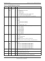
Schematics . . . . . . . . . . . . . . . . . . . . . . . . . . . . . . . . . . . . . . . . . . . . . . . . . . . . . . . . . . . . . 47
Bill of Materials . . . . . . . . . . . . . . . . . . . . . . . . . . . . . . . . . . . . . . . . . . . . . . . . . . . . . . . . . . 47
29704-EVMD-001-C
Mindspeed Technologies™
Mindspeed Proprietary and Confidential
v
List of Figures
Figure 1-1.
Figure 1-2.
Figure 1-3.
Figure 1-4.
Figure 1-5.
Figure 1-6.
Figure 1-7.
Figure 2-1.
Figure 2-2.
Figure 2-3.
Figure 2-4.
Figure 2-5.
Figure 2-6.
Figure 2-7.
Figure 3-1.
Figure 4-1.
Figure 4-2.
Figure 4-3.
Figure 5-1.
Figure 5-2.
Figure 5-3.
Figure 5-4.
Figure 5-5.
Figure 5-6.
CX29704 EVM System . . . . . . . . . . . . . . . . . . . . . . . . . . . . . . . . . . . . . . . . . . . . . . . . . . . . . . 1
CX29704 EVM Hardware Block Diagram . . . . . . . . . . . . . . . . . . . . . . . . . . . . . . . . . . . . . . . . . 2
CX29704 EVM Top View . . . . . . . . . . . . . . . . . . . . . . . . . . . . . . . . . . . . . . . . . . . . . . . . . . . . . 3
CX29704 EVM Software Block Diagram . . . . . . . . . . . . . . . . . . . . . . . . . . . . . . . . . . . . . . . . . 4
Startup Screen . . . . . . . . . . . . . . . . . . . . . . . . . . . . . . . . . . . . . . . . . . . . . . . . . . . . . . . . . . . . 8
New EVM Data File Screen . . . . . . . . . . . . . . . . . . . . . . . . . . . . . . . . . . . . . . . . . . . . . . . . . . . 9
Open EVM Data File Screen . . . . . . . . . . . . . . . . . . . . . . . . . . . . . . . . . . . . . . . . . . . . . . . . . . 10
CX29704 EVM Jump Start . . . . . . . . . . . . . . . . . . . . . . . . . . . . . . . . . . . . . . . . . . . . . . . . . . 11
Mode Switching Dialog . . . . . . . . . . . . . . . . . . . . . . . . . . . . . . . . . . . . . . . . . . . . . . . . . . . . . 12
EVM GUI Application CX29704.xml . . . . . . . . . . . . . . . . . . . . . . . . . . . . . . . . . . . . . . . . . . . 13
CX29704 Registers Screen . . . . . . . . . . . . . . . . . . . . . . . . . . . . . . . . . . . . . . . . . . . . . . . . . . 15
CX29704 Config Screen . . . . . . . . . . . . . . . . . . . . . . . . . . . . . . . . . . . . . . . . . . . . . . . . . . . . 17
CX29704 FM Screen . . . . . . . . . . . . . . . . . . . . . . . . . . . . . . . . . . . . . . . . . . . . . . . . . . . . . . . 18
CX29704 PM Screen . . . . . . . . . . . . . . . . . . . . . . . . . . . . . . . . . . . . . . . . . . . . . . . . . . . . . . . 19
CX29704 EVM Software Block Diagram . . . . . . . . . . . . . . . . . . . . . . . . . . . . . . . . . . . . . . . . 20
CX29704 EVM Component Placement . . . . . . . . . . . . . . . . . . . . . . . . . . . . . . . . . . . . . . . . . 23
CX29704 EVM Hardware Block Diagram . . . . . . . . . . . . . . . . . . . . . . . . . . . . . . . . . . . . . . . . 24
JTAG Test Chain . . . . . . . . . . . . . . . . . . . . . . . . . . . . . . . . . . . . . . . . . . . . . . . . . . . . . . . . . . 27
Packet/ATM FPGA . . . . . . . . . . . . . . . . . . . . . . . . . . . . . . . . . . . . . . . . . . . . . . . . . . . . . . . . . 29
FPGA Context Diagram . . . . . . . . . . . . . . . . . . . . . . . . . . . . . . . . . . . . . . . . . . . . . . . . . . . . . 35
CX29704 EVM Packet/ATM FPGA Block Diagram . . . . . . . . . . . . . . . . . . . . . . . . . . . . . . . . . 36
CX29704 PACKET/ATM FPGA: INTERFACES, DATAFLOW, and CLOCKING . . . . . . . . . . . . . 37
OH FPGA I/O Signals . . . . . . . . . . . . . . . . . . . . . . . . . . . . . . . . . . . . . . . . . . . . . . . . . . . . . . . 42
Clock Selection Subsystem Block Diagram . . . . . . . . . . . . . . . . . . . . . . . . . . . . . . . . . . . . . . 43
29704-EVMD-001-C
Mindspeed Technologies™
Mindspeed Proprietary and Confidential
vi
List of Tables
Table 1-1.
Table 4-1.
Table 4-2.
Table 5-1.
Table 5-2.
Table 5-3.
Table 5-4.
Table 5-5.
Table 5-6.
Table 5-7.
Contents . . . . . . . . . . . . . . . . . . . . . . . . . . . . . . . . . . . . . . . . . . . . . . . . . . . . . . . . . . . . . . . . . 5
CX29704 EVM Memory Map . . . . . . . . . . . . . . . . . . . . . . . . . . . . . . . . . . . . . . . . . . . . . . . . 26
JTAG Signal Description . . . . . . . . . . . . . . . . . . . . . . . . . . . . . . . . . . . . . . . . . . . . . . . . . . . . 27
POS PHY/UTOPIA 2 Transmit CX29704 Side Interface . . . . . . . . . . . . . . . . . . . . . . . . . . . . . 30
POS PHY/UTOPIA 2 Receive CX29704 Side Interface . . . . . . . . . . . . . . . . . . . . . . . . . . . . . 31
System Side POS PHY 2 /UTOPIA Transmit interface . . . . . . . . . . . . . . . . . . . . . . . . . . . . . 32
System Side POS PHY2/UTOPIA Receive interface . . . . . . . . . . . . . . . . . . . . . . . . . . . . . . . 33
HDLC Interface Signal Description . . . . . . . . . . . . . . . . . . . . . . . . . . . . . . . . . . . . . . . . . . . . 34
Packet/ATM FPGA Registers . . . . . . . . . . . . . . . . . . . . . . . . . . . . . . . . . . . . . . . . . . . . . . . . . 40
OH FPGA Registers . . . . . . . . . . . . . . . . . . . . . . . . . . . . . . . . . . . . . . . . . . . . . . . . . . . . . . . . 44
29704-EVMD-001-C
Mindspeed Technologies™
Mindspeed Proprietary and Confidential
vii
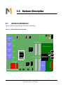
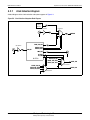
1.0 Getting Started
1.1
Introduction
The CX29704 EVM is a fully integrated platform for evaluating the Mindspeed Technologies CX29704 device -- an
OptiPHY-F155 STS-3/STM-1 SONET/SDH ATM/POS Framer. The CX29704 EVM includes the CX29704TAP
software program, a full featured driver available in C source code form under license from Mindspeed
Technologies.
1.1.1
System Overview
The development system consists of the CX29704 EVM connected to a power supply and a desktop PC or laptop,
which runs the EVM GUI. This is shown in Figure 1-1.
Figure 1-1. CX29704 EVM System
Power Supply
5V
(Optional Test Equipment)
OptiPHYOC-3
CX29704
OC-3
FPGAs
Utopia/POS L2
4
Utopia L2 Tester
POS L2 Tester
Communications /
CPU Subsystem
USB or 10/100 T
EVM GUI
29704-EVMD-001-C
Mindspeed Technologies™
Mindspeed Proprietary and Confidential
1
CX29704 EVM User Manual
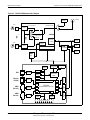
1.1.2
OptiPHY-F155 STS-3/STM-1 SONET/SDH ATM/POS Framer
Hardware Overview
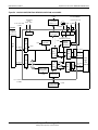
Figure 1-2 depicts the EVM hardware architecture.
Figure 1-2. CX29704 EVM Hardware Block Diagram
19.44 MHz
Oscillator
OC-3
XCVR
4
Reference Clock
Recovered CLK 0
SONET/SDH
Framer
CX29704
4
Tx Clock Select
(Per-Port)
Utopia L2 /
Utop/POS
L2 Tester
POS-L2
DCC / ASSI
Interface
OC-3
XCVR
SONET/SDH
Framer
19.44MHz
Recovered CLK 3
FPGA
Microprocessor I/F
POS L2
Tester
Packet/ATM
ATM L2
Tester
FPGA
(OH)
SDRAM
(SODIMM)
EVM µP Interface
EVM SCC
EEPROM
USB
XCVR
EVM Control
FLASH
Memory
EPLD
XCVR
PowerPC Bus
SCC2
FCC2
I/O
MPC8260
XCVR
Communications Processor
SMC1
SMC2
FCC1
PCI / Local Bus
JTAG
XCVR
SDRAM
Emulator
Utopia L2
COM2
(RS-232)
FCC3
HDLC
COM1
(RS-232)
User I/O
Ethernet
(10/100)
FPGA
PCI Connector (optional)
29704-EVMD-001-C
Mindspeed Technologies™
Mindspeed Proprietary and Confidential
2
CX29704 EVM User Manual
1.1.2.1
OptiPHY-F155 STS-3/STM-1 SONET/SDH ATM/POS Framer
EVM Top View
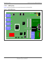
Figure 1-3 illustrates the component and connector placement for the CX29704 EVM.
Port 0 Optical
Module
OP1
1.5V
Reg.
3.3V
Reg.
5.0V
3.3V
3.3VDUT
1.8V
1.5V
DUT
3.3V
Reg.
DUT
RESET
RESET
Figure 1-3. CX29704 EVM Top View
On/OFF
S1
+5Vdc
Fuse
F1
SD0
D10
FPGA POS-PHY L2
Port 1 Optical
Module
OP2
Port 2 Optical
Module
OP3
Port 3 Optical
Module
OP4
SD1
D11
Elgin CPU Subsystem
Packet/ATM
FPGA
J6
J7
USB
SD2
D13
Reset
RX
CX29704
RS-232
TX
CPU
CX29704 UTOPIA/POS-PHY L2
SD3
D21
Status LEDs
RX
TX
J9
J10
MPC8260
J31
OH
FPGA
SODIMM
EXT CLK FPGA CLK
In
In
FPGA CLK
Out
1.8V
Reg.
E-Net
100Mbit
Active
Debug
LED0
LED1
LED2
LED3
LED4
LED5
LED6
LED7
MINDSPEED CX29704 EVM
29704-EVMD-001-C
Mindspeed Technologies™
Mindspeed Proprietary and Confidential
3
CX29704 EVM User Manual
1.1.3
OptiPHY-F155 STS-3/STM-1 SONET/SDH ATM/POS Framer
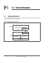
Software Architecture
The CX29704 EVM software consists of code running on the EVM and code running on the Host PC. Figure 1-4
illustrates the software components.
Figure 1-4. CX29704 EVM Software Block Diagram
Host PC
EVM Graphical User Interface (GUI)
Communications
Communications
EVM Application Software
EVM
CX29704TAP Driver
FPGA Drivers
VxWorks RTOS
1.1.3.1
EVM Software Graphical User Interface (GUI)
The EVM software package provides a Graphical User Interface (GUI) application to communicate with the EVM
hardware module. The GUI provides a means to configure the CX29704 and FPGA devices, acquire status
information, collect performance monitoring data, and directly read/write device registers. The GUI uses a TCP/IP
sockets based connection to exchange messages with the embedded TAP drivers that reside on the EVM.
1.1.4
Reference Documents
1.1.4.1
Mindspeed Technologies Documents
1. 29704-DSH-001-X, CX29704 Data Sheet
2. 29704-SWG-002-X, CX29704TAP Software Programming Guide
29704-EVMD-001-C
Mindspeed Technologies™
Mindspeed Proprietary and Confidential
4
CX29704 EVM User Manual
1.2
OptiPHY-F155 STS-3/STM-1 SONET/SDH ATM/POS Framer
Unpacking
The contents of the EVM shipping box should contain, at a minimum, the following items:
Table 1-1. Contents
Qty
Description
1
CX29704 EVM
1
120 VAC / 5VDC Power Converter
1
CX29704 EVM User Manual
2
SC-SC Fiber Optic Patch Cable
1
10/100T Ethernet Cable (straight-through for connection to switch or hub)
1
10/100T Ethernet Cross-Over Cable (cross-over for direct connection to a PC)
1
RS-232 Cable (straight-through for connection to PC serial port)
1
DB9/RJ12 Adaptor
1
CD-ROM containing device and software documentation, hardware schematics and BOM
1.3
Requirements
The following external peripherals are required to support the CX29704 system:
•
•
•
PC System Requirements:
• Any of the following operating systems: Windows 98, NT, 2000 or XP
• 40 MB available Hard drive space
• VT100-compatible monitor (eg., Windows Terminal, HyperTerminal, XTERM)
• 10/100T Ethernet card
OC-3 Test Equipment
ESD-safe workstation
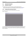
1.4
Installation Procedures
The CX29704 EVM is shipped in nearly “plug-and-play” condition.
The following setup procedures should take no longer than a few minutes.
1.4.1
Hardware Assembly
1.4.1.1
Handling
Normal ESD precautions should be practiced when handling and operating the CX29704 EVM.
1.4.1.2
Board Assembly
The CX29704 EVM is a pre-assembled two module set and no additional assembly is required.
1.4.1.3
Flash Memory
With the exception of occasional FlashROM upgrades to the EVM, there should never be a need to remove or
replace socketed components from the module.
29704-EVMD-001-C
Mindspeed Technologies™
Mindspeed Proprietary and Confidential
5
CX29704 EVM User Manual
1.4.2
OptiPHY-F155 STS-3/STM-1 SONET/SDH ATM/POS Framer
Setting the IP Address
Before using the GUI software, the IP address of the EVM should be changed to one that is appropriate for the
Ethernet LAN to which it will be attached. This is accomplished through the serial port of the EVM. The serial port
settings are 9600 baud, 8 data bits, no-parity and 1 stop bit.
Follow these steps to change the default IP address to a local IP address:
1. Connect to the EVM serial port, connect and apply power. Press and hold the CPU reset switch to reset the
board. Access the debug menu by pressing the <return> key when prompted and before the time-out period
expires. The following text is displayed:
VxWorks System Boot
Copyright 1984-1998
Wind River Systems, Inc.
CPU: MPC8260
CPLD: N-04 - Mindspeed Elgin Version: 5.4.2
BSP version: 2.0/00
Creation date: Jan 29 2003, 14:07:02
Press any key to stop auto-boot...
1
29704-EVMD-001-C
Mindspeed Technologies™
Mindspeed Proprietary and Confidential
6
CX29704 EVM User Manual
OptiPHY-F155 STS-3/STM-1 SONET/SDH ATM/POS Framer
2. Enter ‘c’ and continue hitting <return> until the “inet on ethernet” field is displayed. Enter the new IP address as
show below. Then continue to hit <return> until the boot prompt is redisplayed.
[VxWorks Boot]: c
'.' = clear field;
'-' = go to previous field;
^D = quit
boot device
: flash0
processor number
: 0
host name
: host
file name
: aurora.bin
inet on ethernet (e) : 10.1.158.112 10.1.158.123
inet on backplane (b):
host inet (h)
: 10.1.158.127
gateway inet (g)
: 10.1.158.1
user (u)
:
ftp password (pw) (blank = use rsh):
flags (f)
: 0x88
target name (tn)
:
startup script (s)
:
other (o)
: motfcc
[VxWorks Boot]:
3. Reboot the EVM by entering a ‘@’. When the board comes out of reset, do not enter the debug menu. After the
debug menu prompt times out, the board will load its application software and begin waiting for messages from
the EVM GUI software.
[VxWorks Boot]: @
1.4.3
Installing the EVM GUI software
Follow these steps to install the EVM GUI software:
1. Place the EVM GUI software distribution CD into the CD drive.
2. Run the program “installer.exe” on the CD. A MS-DOS window appears and installs the program files to the
c:\cx29704evm directory. This directory is fixed and can’t be changed. A list of the subdirectories and files
installed is printed to the screen, and then the following prompt:
To launch the application, please do one of the following:
a. Double click desktop icon labeled "CX29704 EVM GUI"
b. At the command prompt, change to C:\cx29704evm directory and type "go"
c. Under window explorer, go to C:\cx29704evm\ directory and double click "go" or
"go.bat"
Do you want to launch the application now (Y/N)?
3. If the necessary Java Virtual Machine is not already loaded on the PC, the installer will issue a prompt to load
the JVM.
4. After pressing any key to continue, a console window appears and the GUI application automatically launches,
displaying the Startup Screen illustrated in Figure 1-5.
29704-EVMD-001-C
Mindspeed Technologies™
Mindspeed Proprietary and Confidential
7
CX29704 EVM User Manual
OptiPHY-F155 STS-3/STM-1 SONET/SDH ATM/POS Framer
1.5
Quick Start Procedure
1.5.1
Running the software
If the EVM GUI software has already been installed, run the software by following these steps:
•
Execute the “go.bat” batch file in the c:\cx29704evm directory. The EVM GUI software run screen will be
displayed and the GUI application will launch, displaying the Startup Screen illustrated in Figure 1-5.
1.5.2
Startup Screen and loading a data file
After the EVM GUI application is launched, the following Startup Screen is displayed:
Figure 1-5. Startup Screen
The EVM GUI application uses a data file containing all of the information necessary to restore parameter settings.
Users can either create a new data file using the EVM template file CX29704EVM.xml or alternatively, open a
previously saved data file. The first time the GUI is started, the “New” option must be selected. All EVM data files
will have a .ser extension.
29704-EVMD-001-C
Mindspeed Technologies™
Mindspeed Proprietary and Confidential
8
CX29704 EVM User Manual
1.5.2.1
OptiPHY-F155 STS-3/STM-1 SONET/SDH ATM/POS Framer
New EVM file
Create a new EVM data file by following these steps:
1. Select the “New” item under the “File” menu. The following screen is displayed:
Figure 1-6. New EVM Data File Screen
2. Select the CX29704ATMEVM.xml file in the browser pane. The file will be highlighted in the “File Name” text
box.
3. Click the “Open” command button.
4. The Jump Start Screen is displayed. See Section 2.1.
29704-EVMD-001-C
Mindspeed Technologies™
Mindspeed Proprietary and Confidential
9
CX29704 EVM User Manual
1.5.2.2
OptiPHY-F155 STS-3/STM-1 SONET/SDH ATM/POS Framer
Existing EVM File
Load an existing data file by following these steps:
1. Select the “Open” item under the “File” menu. The following screen is displayed:
Figure 1-7. Open EVM Data File Screen
2. Select an EVM Serialization file in the browse pane. The file will be highlighted in the “File Name” text box.
3. Click the “Open” command button.
4. The Jump Start Screen in displayed. See Section 2.1.
29704-EVMD-001-C
Mindspeed Technologies™
Mindspeed Proprietary and Confidential
10
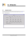
2.0 GUI Operation
2.1
Jump Start Screen
The Jump Start Screen allows easy access to commonly used functions to provision all or any one of the four
tributary channels on the CX29704. The default values for all of the parameters are shown in Figure 2-1.
Figure 2-1. CX29704 EVM Jump Start
29704-EVMD-001-C
Mindspeed Technologies™
Mindspeed Proprietary and Confidential
11
CX29704 EVM User Manual
OptiPHY-F155 STS-3/STM-1 SONET/SDH ATM/POS Framer
At this point, the GUI is in offline mode. Switch to online mode by following these steps:
1. Select the “Online” item under the “Edit” menu. The following screen is displayed:
Figure 2-2. Mode Switching Dialog
2. Enter the IP address of the EVM.
3. Select the desired UTOPIA bus clock source. To use the timing source present on the EVM, select “On Board.”
To use a clock supplied via the UTOPIA connector, select “Connector.”
4. Select the desired software settings synchronization option. The recommended option resets the EVM and GUI
to default settings.
5. Click the “OK” command button.
6. Four screens (as illustrated below in Figure 2-3) are displayed: the Jump Start, CX29704 Registers, OH FPGA
Registers and ATM FPGA Registers.
29704-EVMD-001-C
Mindspeed Technologies™
Mindspeed Proprietary and Confidential
12
CX29704 EVM User Manual
OptiPHY-F155 STS-3/STM-1 SONET/SDH ATM/POS Framer
Figure 2-3. EVM GUI Application CX29704.xml
The “All Tribs” column in the Jump Start Screen can be used to set a parameter to the same value on all the
channels of CX29704. The remaining columns configure an individual channel.
2.1.1
Payload Contents
The payload contents determine whether ATM cells or Packet over SONET is transported over the channels. This
setting affects all channels in the device; therefore, it can only be selected under the All Tribs column
2.1.2
Framing Format
The framing format for the optical signal can either be SONET (STS-3c) or SDH (STM-1).
2.1.3
Timing Source
A channel’s transmit data timing source can be set to either:
•
•
Ref Clock - Timing based on an onboard clock source.
Loop Timing - Timing based on the clock recovered from the receive signal.
29704-EVMD-001-C
Mindspeed Technologies™
Mindspeed Proprietary and Confidential
13
CX29704 EVM User Manual
2.1.4
OptiPHY-F155 STS-3/STM-1 SONET/SDH ATM/POS Framer
Loopback
There are five loopback options on the Jump Start Screen:
•
•
•
•
•
Off - Disables loopback on the channel.
Line - Enables a remote line loopback within the CX29704.
Payload - Enables a remote payload loopback within the CX29704. The CX29704 datasheet refers to this
loopback as a SONET loopback.
Terminal - Enables a local ATM/POS loopback within the CX29704.
FPGA - Enables a remote loopback within the Packet/ATM FPGA of data received over the UTOPIA/POS-PHY
interface.
2.1.5
Packet/ATM FPGA Mode
There are three modes of operation for the Packet/ATM FPGA:
•
•
•
Disabled - Disables the Packet/ATM FPGA, allowing test equipment to be attached to the UTOPIA/POS-PHY
Level 2 connectors (J9/J10).
Utopia - Enables the Utopia interface on the Packet/ATM FPGA.
POS2 - Enables the POS_PHY interface on the Packet/ATM FPGA.
2.1.6
Log Pane
When parameters are changed in the Jump Start Screen, a series of commands are sent to the EVM to configure
the devices. These commands will appear in the Log Pane at the bottom of the Jump Start screen.
29704-EVMD-001-C
Mindspeed Technologies™
Mindspeed Proprietary and Confidential
14
CX29704 EVM User Manual
2.2
OptiPHY-F155 STS-3/STM-1 SONET/SDH ATM/POS Framer
CX29704 Registers Screen
The CX29704 Registers Screen allows the user to read and write any register in the CX29704. All register
addresses and values are in hexadecimal format.
Figure 2-4. CX29704 Registers Screen
2.2.1
Reading a register
Reading a register is a non-invasive operation and will not influence the operation of the embedded driver.
To read a register, follow these steps:
1. Enter the register address to be read in the “Register” dialogue box.
2. Click the “Read” command button.
3. The register value will appear in the “Value” dialogue box.
A register can also be viewed via the Update command.
29704-EVMD-001-C
Mindspeed Technologies™
Mindspeed Proprietary and Confidential
15
CX29704 EVM User Manual
2.2.2
OptiPHY-F155 STS-3/STM-1 SONET/SDH ATM/POS Framer
Writing a register
Writing a register is an invasive operation and could influence the operation of the embedded driver. It bypasses
the normal driver execution. This may lead to nondeterministic results in the execution of the driver.
To write a register, follow these steps:
1.
2.
3.
4.
Enter the register address to be written in the “Register” dialogue box.
Enter the value to write to the specified register in the “Value” dialogue box.
Click the “Write” command button.
The new value will be written to the register. This action can be confirmed by reading back the value via the
read register process or clicking the “Update” command button and viewing the new value in the register
display window.
2.2.3
Update command
All of the register values since the last update are listed in the register display window. To force a refresh of these
values manually, follow these steps:
1. Click the “Update” command button. The register display values will be refreshed.
Any register values that have changed since the last update will be highlighted in red.
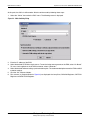
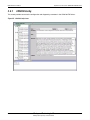
2.3
Packet/ATM FPGA Registers Screen
The Packet/ATM FPGA Registers screen allows the user to read and write the various registers in the Packet/ATM
FPGA. Reading and writing a register is done in the same manner as described in Section 2.2.
2.4
OH FPGA Registers Screen
The OH FPGA Registers screen allows the user to read and write the various registers in the OH FPGA. Reading
and writing a register is done in the same manner as described in Section 2.2.
2.5
TAP Driver Parameter Screens
Additional screens can be enabled via the “Windows” menu that provide more detailed access to the configuration
and status of the CX29704 and FPGA devices. These screens provide access to the TAP driver (see section
Section 3.2.3 and Section 3.2.4) parameters. Refer to the CX29704 TAP Software Programming Guide (see
Section 1.1.4) for a description of the CX29704 parameters.
29704-EVMD-001-C
Mindspeed Technologies™
Mindspeed Proprietary and Confidential
16
CX29704 EVM User Manual
2.5.1
OptiPHY-F155 STS-3/STM-1 SONET/SDH ATM/POS Framer
CX29704 Config
This screen provides access to the configuration and diagnostic parameters in the CX29704 TAP driver.
Figure 2-5. CX29704 Config Screen
29704-EVMD-001-C
Mindspeed Technologies™
Mindspeed Proprietary and Confidential
17
CX29704 EVM User Manual
2.5.2
OptiPHY-F155 STS-3/STM-1 SONET/SDH ATM/POS Framer
CX29704 FM
This screen provides access to the failure monitoring parameters in the CX29704 TAP driver.
Figure 2-6. CX29704 FM Screen
29704-EVMD-001-C
Mindspeed Technologies™
Mindspeed Proprietary and Confidential
18
CX29704 EVM User Manual
2.5.3
OptiPHY-F155 STS-3/STM-1 SONET/SDH ATM/POS Framer
CX29704 PM
This screen provides access to the performance monitoring parameters in the CX29704 TAP driver.
Figure 2-7. CX29704 PM Screen
2.5.4
FPGA Config
These screens provide access to the configuration and diagnostic parameters in the FPGA device drivers.
29704-EVMD-001-C
Mindspeed Technologies™
Mindspeed Proprietary and Confidential
19
3.0 Software Description
3.1
Software Architecture
The software developed for the CX29704 EVM consists of code running on the EVM and code running on the Host
PC. Figure 3-1 illustrates the software components.
Figure 3-1. CX29704 EVM Software Block Diagram
Host PC
EVM Graphical User Interface (GUI)
Communications
Communications
EVM Application Software
EVM
CX29704TAP Driver
FPGA Drivers
VxWorks RTOS
29704-EVMD-001-C
Mindspeed Technologies™
Mindspeed Proprietary and Confidential
20
CX29704 EVM User Manual
3.2
OptiPHY-F155 STS-3/STM-1 SONET/SDH ATM/POS Framer
EVM Software
The software running on the EVM is composed of generic software (RTOS, Communications Protocol) and EVM
specific software (EVM Application Software, Device Drivers). The following sections describe the software in more
detail.
3.2.1
RTOS
At the lowest level, the software consists of a VxWorks Real-Time Operating System (RTOS) with a Board Support
Package (BSP) specific to the MPC8260 based CPU subsystem. The RTOS and basic BSP are available from
WindRiver as a licensed source code product. The BSP is customized in small ways to account for the limited
differences between the hardware components on the CPU subsystem and WindRiver’s SBC8260 standard
platform (a Motorola reference design).
3.2.2
Communications
A communications driver / protocol software layer is provided on the EVM to facilitate communications between the
EVM and the host PC. The communications function is provided in part by the RTOS in that it provides TCP/IP and
COM port support. USB extensions are written to enhance the available BSP software. Higher level protocol
software is required for implementing a message set that relies on these lower layers.
3.2.3
CX29704 TAP
The TAP (Telecom Application Program) is a full-featured device driver for the CX29704 family that builds on an
existing line of software products and collateral for Mindspeed WAN Access devices. The TAP software includes a
comprehensive set of software parameters and functions that translate the device control registers and features
into the software realm, plus such value added features as standards compliant Failure Monitoring and
Performance Monitoring.
3.2.4
FPGA Device Driver
For each FPGA device on the EVM, a separate device driver will be included in the EVM software. These drivers
will control and monitor the loopback and other diagnostic features of those devices.
3.2.5
EVM Application Code
In the category of miscellaneous, additional application code and utilities will be provided on the EVM to integrate
the various drivers and software layers. Given the independence of the some of the functions on the module, some
of the high level features of the EVM will be implemented partly on the EVM and partly by software on the host PC.
29704-EVMD-001-C
Mindspeed Technologies™
Mindspeed Proprietary and Confidential
21
CX29704 EVM User Manual
3.3
OptiPHY-F155 STS-3/STM-1 SONET/SDH ATM/POS Framer
Host Software
In addition to the standard Windows operating system running on the host PC, a software program will be executed
that is specific to the Mindspeed EVM product. Similar to the EVM resident software, the Host software will include
EVM generic software and CX29704 EVM specific software.
3.3.1
Communications Protocol
A portion of the EVM Host Software is software for communicating with the EVM. This software relies on Windows
lower layer communications protocols and drivers for transport through the hardware connections to the EVM.
3.3.2
Graphical User Interface (GUI)
The user interface for the EVM is a Java based GUI running on a PC and has the following functionality:
•
•
•
•
•
Device configuration and diagnostics
Failure monitoring
Performance monitoring
Low level register read/write
EVM Test Setup
The GUI provides the user with a view into the CX29704TAP software parameters and the CX29704 device itself
plus adds “macro” functions to ease device setup and configuring of the test capabilities of the EVM. Section 2.0
describes the GUI in more detail.
29704-EVMD-001-C
Mindspeed Technologies™
Mindspeed Proprietary and Confidential
22
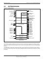
4.0 Hardware Description
4.1
Hardware Architecture
Figure 4-1 shows the component placement on the CX29704 EVM.
Port 0 Optical
Module
OP1
1.5V
Reg.
3.3V
Reg.
5V
3.3V
3.3VDUT
1.8V
1.5V
DUT
3.3V
Reg.
DUT
RESET
RESET
Figure 4-1. CX29704 EVM Component Placement
On/OFF
S1
+5Vdc
Fuse
F1
SD0
D10
FPGA POS-PHY L2
Port 1 Optical
Module
OP2
Port 2 Optical
Module
OP3
Port 3 Optical
Module
OP4
SD1
D11
Elgin CPU Subsystem
Packet/ATM
FPGA
J6
J7
USB
SD2
D13
Reset
RX
CX29704
RS-232
TX
CPU
CX29704 UTOPIA/POS-PHY L2
SD3
D21
Status LEDs
RX
TX
J9
J10
MPC8260
J31
OH
FPGA
SODIMM
EXT CLK FPGA CLK
In
In
FPGA CLK
Out
1.8V
Reg.
E-Net
100Mbit
Active
Debug
LED0
LED1
LED2
LED3
LED4
LED5
LED6
LED7
MINDSPEED CX29704 EVM
29704-EVMD-001-C
Mindspeed Technologies™
Mindspeed Proprietary and Confidential
23
CX29704 EVM User Manual
OptiPHY-F155 STS-3/STM-1 SONET/SDH ATM/POS Framer
Figure 4-2. CX29704 EVM Hardware Block Diagram
19.44 MHz
Oscillator
OC-3
XCVR
4
Reference Clock
Recovered CLK 0
SONET/SDH
Framer
CX29704
4
Tx Clock Select
(Per-Port)
Utopia L2 /
Utop/POS
L2 Tester
POS-L2
DCC / ASSI
Interface
OC-3
XCVR
SONET/SDH
Framer
19.44MHz
Recovered CLK 3
FPGA
Microprocessor I/F
POS L2
Tester
Packet/ATM
ATM L2
Tester
FPGA
(OH)
SDRAM
(SODIMM)
EVM µP Interface
EVM SCC
EEPROM
USB
XCVR
EVM Control
FLASH
Memory
EPLD
XCVR
PowerPC Bus
SCC2
FCC2
I/O
MPC8260
XCVR
Communications Processor
SMC1
SMC2
FCC1
PCI / Local Bus
JTAG
XCVR
SDRAM
Emulator
Utopia L2
COM2
(RS-232)
FCC3
HDLC
COM1
(RS-232)
User I/O
Ethernet
(10/100)
FPGA
PCI Connector (optional)
29704-EVMD-001-C
Mindspeed Technologies™
Mindspeed Proprietary and Confidential
24
CX29704 EVM User Manual
4.1.1
OptiPHY-F155 STS-3/STM-1 SONET/SDH ATM/POS Framer
CX29704
The CX29704 is an integrated circuit that implements four-channel mapping functions for SONET/SDH processing
and ATM/HDLC at 155.52 Mbps. The component contains both the PMD and the TC sublayers and provides an
UTOPIA Level 2 interface for the ATM layer or a POS-PHY Level 2 interface for the link layer. Each port may be
selected on a per port basis for either High Level Data Link Controller (HDLC) or ATM Cell Delineator protocol
options.
The CX29704 line side interfaces support optical OC3/STS-3c.
The system side interface may be chosen from the combination of UTOPIA Level 2 for ATM or POS-PHY Level 2
for HDLC packets. The dual mode Utopia Level 2 / POS Level 2 interface is brought out to a Utopia 2 test
connector and routed to the Packet/ATM FPGA. This FPGA provides POS Level 2 transparency to external POS
Level 2 test equipment. The feature set of this FPGA is described in Section 5.1.
The SONET/SDH Framer block provides access to the STS-3c transport DCC overhead, both insertion and
extraction. The Overhead interfaces of the CX29704 are routed to the OH FPGA which allows access to overhead
information on the STS-3c lines. The feature set of this FPGA is described in Section 5.2.
A full set of loopbacks is provided.
4.1.2
Packet/ATM FPGA
The Packet/ATM FPGA provides a number of functions:
•
•
•
•
•
•
•
•
External UTOPIA L2 Tester access to CX29704 UTOPIA Level 2 Interface
Per-port active transmit UTOPIA interface selection (System L2 interface, Rx port loopback, optional cell
generator)
Per-port Tx and Rx ATM cell counters.
External SPI-2 Tester access to CX29704 POS Level 2 Interface
Full packetization of HDLC traffic
Packet level loopback functionality
CPU subsystem access (serial HDLC stream) to CX29704 POS Level 2 interface
Packet and ATM cell generation and monitoring features (tbd)
4.1.3
Overhead FPGA
The OH FPGA supports the ASSI alarm interface and contains miscellaneous glue logic for the EVM. It also
provides access to the SONET/SDH Transport DCC Overhead for STS-3c interface.
4.1.4
Control Subsystem
The communications and control subsystem is implemented on a daughter board known as the Elgin Processor
Board. Elgin is comprised of an MPC8260 Microprocessor with SDRAM, Flash, EEPROM, Ethernet, USB, and
RS232 serial ports. In customer applications of the EVM, the Ethernet and USB interfaces will be used.
Refer to the Elgin Processor Hardware Description Document for more information.
29704-EVMD-001-C
Mindspeed Technologies™
Mindspeed Proprietary and Confidential
25
CX29704 EVM User Manual
4.1.4.1
OptiPHY-F155 STS-3/STM-1 SONET/SDH ATM/POS Framer
Internal Memory Map
Table 4-1 summarizes the memory map for the CX29704 EVM. The use of the other Chip Select lines are described
in the Elgin Processor documentation.
Table 4-1. CX29704 EVM Memory Map
Chip Select
EVM Base Address
Address Space Required
Function
CS8#
CS9#
CS11#
0xB0000000
0xD0010000
0xD0020000
128 KByte
64 KByte
64 KByte
CX29704 Device
Packet/ATM FPGA
Overhead FPGA
4.1.5
Oscillators
The CX29704 EVM employs the following oscillators:
•
•
The CX29704 device uses a 19.44 MHz ±20 ppm oscillator for its CLAD circuit.
The Packet/ATM FPGA uses a 100 MHz ±50 ppm oscillator to generate and receive POS/ATM data.
4.1.6
Power
4.1.6.1
External Power
Power is provided from a +5V/5A regulated tabletop power supply. Typical current draw for the board is 3.8A with
all channels operational.
4.1.6.2
EVM Regulators
Four voltage regulators (from +5V input supply) are implemented on the EVM.
•
•
•
•
+3.3V Board supply
+3.3V CX29704 supply
+1.8V Overhead FPGA core voltage
+1.5V Packet/ATM FPGA core voltage
Status LEDs for all supply voltages are provided. If the voltages are below nominal, the board will be held in reset.
The 3.3V regulators turn on first, followed by the FPGA core voltage regulators. Enable timing is adjustable by
changing a voltage divider and capacitive loading on the regulator enable pin.
As a build option, the board 3.3V and CX29704 3.3V supplies can be tied together by removing the CX29704
regulator and connecting the planes via a ferrite bead. These options allow the verification of various power
schemes that customers may wish to implement.
Dual regulators for the board 3.3V and CX29704 3.3V are provided to allow individual control of the supply
voltages. The regulators used are all the same adjustable regulator to minimize the number of different
components used. They are placed on generic dual TO-263-5/TO-220-5 footprints.
Removal of R250 allows for placing an ammeter across J1 and J2 to measure the current to the CX29704 device.
As an additional build option, the CX29704 3.3V may be sourced from an external supply.
29704-EVMD-001-C
Mindspeed Technologies™
Mindspeed Proprietary and Confidential
26
CX29704 EVM User Manual
OptiPHY-F155 STS-3/STM-1 SONET/SDH ATM/POS Framer
4.2
Line-Side Interface
4.2.1
Optical Front-End
The EVM line-side interface consists of four Luminent 1310 nm single-mode optical transceivers, in an SC1x9
package. Signal Detect signals from each of the four transceiver modules are indicated by individual LEDs. All
signals between the transceiver modules and the CX29704 device are LVPECL levels.
4.3
Electrical Interfaces
4.3.1
Signal Description
In Table 4-2, the following definitions are used:
Loc
Type
Physical Location of the I/O signal
Classification of signal (C -- 3.3V CMOS compatible input or output, CT -- 3.3V CMOS Tristateable output, F - DS3/E3/
STS-1E facility, R -- RS232 compatible input or output, E -- 10/100 BaseT input or output, U -- USB, P -- VDD or VSS)
Signal Flow direction (I=Input, O=Output, IO=Bidirectional)
Dir
4.3.2
JTAG
Connector P1 is the JTAG connector on the EVM. It is used to perform boundary scan test on the board using the
standard Corelis pin-out. This JTAG connector connects to a single chain of all of the JTAG compliant devices on
the board.
Any of these parts can be removed from the chain by removing the 33 ohm resistor at the device’s output and
installing the zero ohm resistor to bypass the part.
Figure 4-3. JTAG Test Chain
not installed
0
BDM
TDI
TMS
TRST
not installed
not installed
0
33
TCK
0
33
Packet
TMS FPGA
CX29704
0
TCK
33
TX
TMS
TRST
TCK
not installed
RAM
TMS
TRST
TCK
0
33
33
RX
RAM
OH FPGA
TMS
TRST
TCK
TDO
P1 provides a 10 pin connector for use with standard JTAG controllers.
Table 4-2. JTAG Signal Description
Name
TRST
TDI
TDO
TMS
TCK
29704-EVMD-001-C
Loc.
Type
Dir
P4-1
P4-3
P4-5
P4-7
P4-9
C
C
C
C
C
I
I
O
I
I
Description
JTAG Reset
JTAG Serial Data Input
JTAG Serial Data Output
JTAG Mode Select
JTAG Clock
Mindspeed Technologies™
Mindspeed Proprietary and Confidential
27
CX29704 EVM User Manual
4.3.3
OptiPHY-F155 STS-3/STM-1 SONET/SDH ATM/POS Framer
Test Points
Connectors P2 and J8 are test points for FPGA development.
4.3.4
UL2 Connectors
Connectors J6 and J7 are connectors for interfacing standard UTOPIA test equipment (Adtech AX4000, Innocor
Phymaster) to the FPGA. Connectors J9 and J10 are connectors for interfacing standard UTOPIA test equipment
directly to the CX29704 UTOPIA bus.
4.3.5
Power Interface
The CX29704 EVM accepts +5V through J3/J4.
4.4
Other Interfaces
4.4.1
LEDs
The following LEDs are provided.
•
•
•
•
•
•
•
•
•
RESET: A Green LED indicates hardware reset when illuminated.
DUT_RESET: A Green LED indicates CX29704-only reset when illuminated.
5V, 3.3V DUT, 1.5V, 1.8V: A Green LED indicates that the indicated power supply voltage is above the
minimum acceptable value.
LED0 - LED3: Packet/ATM FPGA LEDs for development
PHYMASTER: Indicates J9 and J10 are configured for use with Innocor Phymaster test pods.
ADTECH: Indicates J9 and J10 are configured for use with Adtech AX4000 Utopia test pods.
UTOPIA: Indicates J9 and J10 are configured for operation with ATM test pods.
POS: Indicates J9 and J10 are configured for operation with POS test pods.
SD0 - SD3: A Yellow LED indicates receive signal detected at the optical interface.
The following LEDs are controlled by the CX29704 ASSI interface:
•
•
•
•
•
•
•
•
•
•
•
•
TXC-P0 - TXC-P3: Indicates transmitted cells or packets when illuminated.
RXC-P0 - RXC-P3: Indicates received cells or packets when illuminated.
LCD0 - LCD3: Indicates LOCD when illuminated.
P-SD0 - P-SD3: Indicates P-SD when illuminated
P-SF0 - P-SF3: Indicates P-SF when illuminated.
LOP0 - LOP3: Indicates LOP when illuminated.
AIS-P0 - AIS-P3: Indicates AIS-P when illuminated.
L-SD0 - L-SD3: Indicates L-SD when illuminated.
L-SF0 - L-SF3: Indicates L-SF when illuminated.
AIS-L0 - AIS-L3: Indicates AIS-L when illuminated.
LOF0 - LOF3: Indicates LOF when illuminated.
LOS0 - LOS3: Indicates LOS when illuminated.
4.4.2
Jumpers
There are no jumpers to set on the board.
29704-EVMD-001-C
Mindspeed Technologies™
Mindspeed Proprietary and Confidential
28
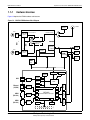
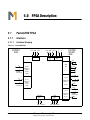
5.0 FPGA Description
5.1
Packet/ATM FPGA
5.1.1
Interfaces
5.1.1.1
Functional Grouping
Figure 5-1. Packet/ATM FPGA
CX29704
SIDE
CNTL ADDR
DATA
CNTL ADDR
8
100M 50M 25M
clk
DATA clk clk
SYSTEM
TESTER
SIDE
18
SRAM
INTF
Tx
µP
DLL
INTF
CD#
RxD
4
HDLC
16
Transmit
INTF
DATA
CONTROL
SOP,EOP, ETC
POS-PHY 2/
UTOPIA 2
Interface
4
TxD
RTS#
CTS#
50MHz
8 or16
16
Transmit
Receive
POS-PHY 2/
DATA
CONTROL
SOP,EOP, ETC
POS-PHY 2/
UTOPIA 2
Interface
UTOPIA 1, 2
Interface
DATA
CONTROL
SOP,EOP, ETC
CLOCK
50MHz
8 or16
DATA
Receive
POS-PHY 2/
UTOPIA 1,2
TESTPOINTS
&
LEDs
SRAM
INTF
Rx
Interface
CONTROL
SOP,EOP, ETC
CLOCK
18
LEDs
29704-EVMD-001-C
TSTPNTS
CNTL ADDR
Mindspeed Technologies™
Mindspeed Proprietary and Confidential
DATA
29
CX29704 EVM User Manual
5.1.1.2
OptiPHY-F155 STS-3/STM-1 SONET/SDH ATM/POS Framer
Signal Description
In Table 5-1 - Table 5-5, the following definitions are used:
Loc
Physical Location of the I/O signal
Type
Classification of signal (C -- 3.3V CMOS compatible input or output, CT -- 3.3V CMOS Tristateable output, P -- VDD or VSS)
Dir
Signal Flow direction (I=Input, O=Output, IO=Bidirectional, Z=high impedance)
All signals are active high except for signal names ending in the symbol “#”.
5.1.1.2.1
CX29704 Interface
The signals in Table 5-1 connect directly to the CX29704 device.
Table 5-1. POS PHY/UTOPIA 2 Transmit CX29704 Side Interface
Name
Loc.
Type
Dir
Description
P18
CT
O or Z
The TENB signal (active low) is used to initiate writes to selected ports.
POS & UTOPIA.
R18,R19,R20,R21
R22,T18,T19,T20
T21,T22,U18,U19
U20,U21,U22,V22
CT
O orZ
Transmit packet-cell data bus[15:0] POS & UTOPIA.
TPRTY_U2_LE
AA202
CT
O or Z
Calculated parity for the TDAT_U2_LE bus. POS & UTOPIA.
TSOP_U2_LE
W22
CT
O or Z
TSOP/SOC indicates the first word of a packet. POS & UTOPIA
AA18,V19,V20,V21,
W21
CT
O or Z
The TADR[4:0] bus is used to select the port that is written to using the
TENB signal, and the ports' whose packet available signal is visible on
the TPA output when polling. POS & UTOPIA
PTPA_U2_LE
AB18
C
I
PTPA/TCLAV transitions high when a predefined minimum number of
bytes is available in the polled transmit port's FIFO. Once high, PTPA
indicates that the transmit port's FIFO is not full. When PTPA transitions
low, it optionally indicates that the transmit FIFO is full or near full
(normally user programmable). PTPA allows to poll the port address
selected by TADR[4:0] when TENB is asserted. PTPA is driven by a port
when its address is polled on TADR[4:0]. POS & UTOPIA.
TMOD_U2_LE
W20
CT
O or Z
TMOD indicates the size of the current word. POS only.
TEOP_U2_LE
Y21
CT
O or Z
TEOP marks the end of a packet on the TDAT[15:0] bus. POS only.
TERR_U2_LE
Y22
CT
O or Z
TERR is used to indicate that the current packet is aborted and should
be discarded. POS only.
STPA_U2_LE
P17
C
I
STPA transitions high when a predefined minimum number of bytes is
available in the selected transmit port's FIFO . Once high, STPA
indicates that the transmit FIFO is not full. When STPA transitions low, it
optionally indicates that the transmit FIFO is full or near full. STPA
always provide status indication for the selected port in order to avoid
FIFO overflows while polling is performed. POS only.
TXENB_U2_LE#
TDAT_U2_LE[15:0]
TADR_U2_LE[4:0]
29704-EVMD-001-C
Mindspeed Technologies™
Mindspeed Proprietary and Confidential
30
CX29704 EVM User Manual
OptiPHY-F155 STS-3/STM-1 SONET/SDH ATM/POS Framer
The signals in Table 5-2 directly connect to the CX29704 device.
Table 5-2. POS PHY/UTOPIA 2 Receive CX29704 Side Interface
Name
Loc.
Type
Dir
A7
CT
O or Z
The RENB signal is used to initiate reads from the receive FIFO's (in
CX29704). When RENB is asserted data is transferred from the selected
PHY and RADR[4:0] is used to select the PHY. POS & UTOPIA.
RADR_U2_LE[4:0]
K1,K2,K3,K4
K6
CT
O or Z
The RADDR is used to select the PHY device (or port number) in which
the system (FPGA) wants to read data from, this done by placing the
appropriate address on RADDR one cycle before asserting RENB. POS &
UTOPIA.
RDAT_U2_LE[15:0]
F1,F2,F3,F4
G1,G2,G3,G4
H1,H2,H3,H4
J1,J2,J3,J4
C
I
The RDATA[15:0] bus carries the packet-cell words that are read from the
selected port. POS & UTOPIA.
RPRTY_U2_LE
A6
C
I
The receive parity (RPRTY) signal indicates the parity of the RDAT bus.
POS & UTOPIA
RSOP_U2_LE
B7
C
I
RSOP marks the first word of a packet-cell transfer. POS & UTOPIA
PRPA_U2_LE
C7
C
I
PRPA (AKA RCALV) indicates when data is available in the polled port.
When PRPA is high, the port has at least one end of packet-cell or a
predefined number of bytes to be read. POS & UTOPIA
RMOD_U2_LE
B6
C
I
RMOD indicates the number of bytes carried by the RDATA[15:0] bus
during the last word of a packet transfer. POS only
RVAL_U2_LE
D7
C
I
RVAL indicates the validity of the receive data signals. When RVAL is high,
the receive signals RDAT, RSOP, REOP, RMOD, RPRTY and RERR are
valid. POS only.
RERR_U2_LE
C6
C
I
RERR is used to indicate that the current packet is aborted and should be
discarded. POS only.
REOP_U2_LE
E7
C
I
REOP marks the end of packet on the RDATA[15:0] bus. POS & UTOPIA.
RENB_U2_LE#
29704-EVMD-001-C
Description
Mindspeed Technologies™
Mindspeed Proprietary and Confidential
31
CX29704 EVM User Manual
5.1.1.2.2
OptiPHY-F155 STS-3/STM-1 SONET/SDH ATM/POS Framer
SYSTEM SIDE POS PHY 2 INTERFACE
Table 5-3. System Side POS PHY 2 /UTOPIA Transmit interface
Name
Loc.
Type
Dir
Description
TXENB_U2_SY#
L20
C
I
The TENB signal (active low) is used to initiate writes to selected ports.
POS & UTOPIA.
G19,G20,G21,G22
H19,H20,H21,H22
J19,J20,J21,J22
K19,K20,K21,K22
C
I
Transmit packet/cell data bus[15:0] POS & UTOPIA.
TPRTY_U2_SY
F18
C
I
Calculated parity for the TDAT_U2_LE bus. POS & UTOPIA.
TSOP_U2_SY
F19
C
I
TSOP (a.k.a. SOC) indicates the first word of a packet. POS & UTOPIA.
TEOP_U2_SY
F20
C
I
TEOP marks the end of a packet on the TDAT[15:0] bus. POS only
TERR_U2_SY
F21
C
I
TERR is used to indicate that the current packet is aborted and should
be discarded. POS only.
E18,E19,E20,E21,E
22
C
I
TADR is the mphy address of the channel.POS & UTOPIA.
TMOD_U2_SY
F22
C
I
TMOD indicates the size of the current word. POS only.
TPA_U2_SY
G18
C
O
PTPA (a.k.a. TCLAV) transitions high when a predefined minimum
number of bytes is available in the polled transmit port's FIFO. Once
high, PTPA indicates that the transmit port's FIFO is not full. When
PTPA transitions low, it optionally indicates that the transmit FIFO is
full or near full (normally user programmable). PTPA allows to poll the
port address selected by TADR[4:0] when TENB is asserted (POS only
feature). POS & UTOPIA
STPA_U2_SY
A19
C
O
STPA contains information about the availability of packets in the
selected channel. POS only.
TDAT_U2_SY[15:0]
TADR_U2_SY[4:0]
29704-EVMD-001-C
Mindspeed Technologies™
Mindspeed Proprietary and Confidential
32
CX29704 EVM User Manual
OptiPHY-F155 STS-3/STM-1 SONET/SDH ATM/POS Framer
Table 5-4. System Side POS PHY2/UTOPIA Receive interface
Name
Loc.
Type
Dir
A5
C
I
RENB is used to control the flow of data from the receive FIFOs. POS &
UTOPIA
T1,T2,T3,T4,
T5,U1,U2,U3,
U4,U5,V1,V2,
V3,V4,V5,W1
C
O
Packet/cell data. POS & UTOPIA
RPRTY_U2_SY
B5
C
O
RPRTY indicates the calculated Parity for the current octet. POS &
UTOPIA
RSOP_U2_SY
V6
C
O
RSOP indicates the first word of a packet/cell. POS & UTOPIA
REOP_U2_SY
W6
C
O
REOP indicates the first word of a packet. POS only
RERR_U2_SY
C5
C
O
RERR is used to indicate that the current packet is aborted and should be
discarded. POS only
Y7,R1,R2,R3,
R4
C
I
RADR is the mphy address of the channel. POS & UTOPIA.
RPA_U2_SY
AA5
C
O
RPA (a.k.a. RCLAV) indicates that the polled PHY has a packet or cell to
transfer. POS & UTOPIA.
RMOD_U2_SY
A4
C
O
RMOD indicates the number of valid bytes on the last word. POS only.
RVAL_U2_SY
AB5
C
O
Indicates the validity of the POS-PHY receive data signals. POS only.
RENB_U2_SY#
RDAT_U2_SY[15:0]
RADR_U2_SY[4:0]
29704-EVMD-001-C
Description
Mindspeed Technologies™
Mindspeed Proprietary and Confidential
33
CX29704 EVM User Manual
5.1.1.2.3
OptiPHY-F155 STS-3/STM-1 SONET/SDH ATM/POS Framer
HDLC Interface
Table 5-5. HDLC Interface Signal Description
Name
Loc.
Type
Dir
Description
Note the clock for this interface is provided to the 8260 via the PCB; the 25MHz clock driven by the Packet/ATM FPGA.
TXD[3:0]
H18,C22,K18,C21
C
O
Serial data from the Packet/ATM FPGA to the 8260 FCC
RXD[3:0]
F5,G5,H5,J5
C
I
Serial data from the 8260 FCC to the Packet/ATM FPGA
RTS#
K17
C
O
RTS# indicates the beginning of a frame, and can be used at the receiver for
synchronization.
Note that RTS# and CTS# are used by a peripheral on the serial link by the
corresponding peripherals transmitter. CD# is used by the receiver on the
other end of the link. A typical application would connect the RTS# on
peripheral A to CD# on peripheral B via the serial bus.
Reference the Motorola MPC 8260 users manual chapters 28, and 32 for
details of the timing. There are several combinations of timing, that depend
on the nature of the data being moved. These combinations must be set up in
the 8260 register structure.
CTS#
E5
C
I
CTS# indicates that the receiving end is able to accept data.
Note that RTS# and CTS# are used by a peripheral on the serial link by that
peripherals transmitter. CD# is used by the receiver on the other end of the
link.
CD#
E6
C
I
CD# is used by a peripherals receiver to know when a start of frame is
occurring.
Note that RTS# and CTS# are used by a peripheral on the serial link by that
peripherals transmitter. CD# is used by the receiver on the other end of the
link. A typical application would connect the RTS# on peripheral A to the CD#
on peripheral B.
29704-EVMD-001-C
Mindspeed Technologies™
Mindspeed Proprietary and Confidential
34
CX29704 EVM User Manual
OptiPHY-F155 STS-3/STM-1 SONET/SDH ATM/POS Framer
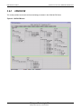
5.1.2
Packet/ATM FPGA Functional Description
5.1.2.1
Block Diagram
Figure 5-2. FPGA Context Diagram
Utopia L2 /
Utopia
Tester
POS-L2
CX29704
FPGA
(Pkt/ATM)
µP Interface
29704-EVMD-001-C
Utopia
Tester
MPC8260
Mindspeed Technologies™
Mindspeed Proprietary and Confidential
35
CX29704 EVM User Manual
OptiPHY-F155 STS-3/STM-1 SONET/SDH ATM/POS Framer
Figure 5-3. CX29704 EVM Packet/ATM FPGA Block Diagram
U2 Tx and Rx CLK
(50MHz)
TO 8260 HDLC
TO/FROM
CPU
Addr Data
Optional ZBT
SRAM (receive)
CX29704
Utopia 2
POS 2
(system side)
µC Intf
Optional ZBT
SRAM Controller
DLL
INTERNAL CLOCKS
POS/
UTP
2
RX_DATA
16
POS
PHY
2
INTF
HDLC
SERDES
and CNTL
CELL-PACKET
MONITOR
RX
RX
FIFOs
TX_DATA
POS
PHY2
UTP
INTF
RX
POS
PHY
2
INTF
16
TX
TX
FIFOs
CELL-PACKET
GENERATOR
POS
PHY2
UTP
INTF
TX
RX_DATA
8 /16
RX_CLK
(25-50)MHz
TX_DATA
POS
PHY2/
UTP
TESTER
8/16
TX_CLK
(25-50)MHz
Optional ZBT
SRAM Controller
Optional ZBT
SRAM (transmit)
29704-EVMD-001-C
Mindspeed Technologies™
Mindspeed Proprietary and Confidential
36
CX29704 EVM User Manual
OptiPHY-F155 STS-3/STM-1 SONET/SDH ATM/POS Framer
Figure 5-4. CX29704 PACKET/ATM FPGA: INTERFACES, DATAFLOW, and CLOCKING
100MHz
U2 Tx and Rx CLK
(50MHz)
TO/FROM
CPU
Addr Data
8
25MHz clk,TXD, RXD,
Optional ZBT
SRAM (receive)
Data
8
µC Intf
50 MHz 25 MHz
Optional ZBT
SRAM Controller
4
4
100 MHz
18
CX29704
Utopia 2
Packet Intf
(system side)
TO 8260 HDLC
DLL1 DLL2 DLL3
100M 50M
INTERNAL CLOCKS
POS
PHY
2
POS
PHY
2
INTF
50MHz
50MHz
CELL-PACKET
MONITOR
HDLC
SERDES
and CNTL
50MHz
RX_DATA
16
RX
18 x 32K
Sync
18 x 16
Async
FIFO
Dual Port
POS
PHY
2
POS2/ RX_DATA
UTP
8/16
INTF
RX
RX_CLK
(25-50)MHz
50 MHz
INTF
TX_DATA
16
18 x 32K
TX
100MHz
50 MHz
(25-50)MHz
Optional ZBT
SRAM Controller
18
Data
Optional ZBT
SRAM (transmit)
29704-EVMD-001-C
POS2/
UTP
INTF
TX
TX_CLK
CELL-PACKET
GENERATOR
100MHz
U3 Tx and Rx CLK
(100MHz)
18 x 16
Async
FIFO
Sync
Dual Port
POS
PHY
2/
UTP
TX_DATA
TESTER
8/16
Mindspeed Technologies™
Mindspeed Proprietary and Confidential
100MHz
37
CX29704 EVM User Manual
5.1.3
Functional Blocks
5.1.3.1
CX29704 Interface
OptiPHY-F155 STS-3/STM-1 SONET/SDH ATM/POS Framer
The Packet/ATM FPGA connects to CX29704 via standard POS-PHY 2 and UTOPIA 2 interfaces. The Packet/
ATM FPGA allows only one CX29704 interface active at a time (SW control). There are 31 (POS-UTOPIA 2)
possible logical channels in which packet data may be transmitted or received; the Packet/ATM FPGA supports
any six physical channels active at a time (SW control). Both packet interfaces are under the control of a single
memory mapped bit that performs a “run-stop” function (default is run), and individual channel enables. Note that
the POS-PHY 2 interface outputs are tristatable to allow other masters on the PCB to communicate with the
CX29704.
Data is continuously accepted by the Packet/ATM FPGA POS2/UTOPIA 2 interface in the Rx direction (subject to
the run-stop bit), even if the FPGA’s buffers are full. No “back pressure” is applied to the POS2/UTOPIA 2 Rx
interface.
One-word packets are discarded in the Rx direction. Two-word or greater length packets are buffered and
forwarded normally. A limitation is imposed by the minimun packet size of the Innocor PHY Master (5 bytes).
Packets received with the err signal asserted are buffered and forwarded with the err signal asserted. This is true in
both Tx and Rx directions.
Parity is calculated at all the interfaces but NOT buffered. Therefore parity errors do not loopback or pass thru the
Packet/ATM FPGA.
5.1.3.2
CX29704 Side Loopback Muxes
The Packet/ATM FPGA provides POS-PHY/UTOPIA 2 channelized loopback under SW control. Note that the
loopbacks pass thru the packet buffers, therefore the full packetization function is active while in loopback. The
loopback muxes also serves as the insertion point for the packet generator to drive packets toward the CX29704.
5.1.3.2.1
Internal Block RAM Used as Packet Buffers
The Packet/ATM FPGA collects packet fragments from the packet interfaces and accumulates them in a buffer
until an entire packet is present. After a full packet is buffered the packet available signal on the system tester side
is asserted. The tester can now remove the packet in its entirety without any pauses on the packet bus. The Xilinx
Virtex II 1000 has enough block RAM to implement six buffers each holding about 1.9K bytes.
If the incoming packet size is larger than the buffer, then the packet will be accepted and truncated to fit in the
buffer, and that packet will be marked by the assertion of the err signal. If a missing end condition is created by
faulty transmission or a switch to loopback mid-packet, the current packet is also marked with an err.
UTOPIA cells are always internally stored 54 bytes in length. This means that false data is inserted into the
incoming stream when accepting 52 or 53 byte cells. Also note that the extra bytes are removed from the outgoing
stream when an outgoing interface is configured as 52 or 53 byte. This is true in both the Tx and Rx directions.
Note that UTOPIA cells are marked with EOP internally using counters. Therefore much of the control logic to
operates as if HDLC packet are being processed. This avoided a complete re-design of the packet based design
when UTOPIA features were added.
5.1.3.2.2
Small Asynchronous FIFOs
Small asynchronous FIFOs are used to decouple the internal and external clocks associated with the packet tester
and the rest of the Packet/ATM FPGA. Data width conversion is done for the UTOPIA interface using control logic
near these fifos and their flags.
29704-EVMD-001-C
Mindspeed Technologies™
Mindspeed Proprietary and Confidential
38
CX29704 EVM User Manual
5.1.3.2.3
OptiPHY-F155 STS-3/STM-1 SONET/SDH ATM/POS Framer
Master Design
The POS/UTOPIA 2 masters poll until a packet available is detected. Next, the transfer of a packet begins. The
master continues to poll while the packet is being transferred. If another channel indicates packet available true,
then that channel number is stored so that the channel will be accessed when the current channel completes its
transfer. The number of channels to poll is programmable using the memory mapped interface.
5.1.3.2.4
FPGA System Side Interface
The system side interface to the external test set is configured as a POS-PHY2 or UTOPIA 1/2 slave. The POS 2
interface will delay assertion of the packet available signal until there is at least one EOP in the buffer.
5.1.3.2.5
Packet Monitor
Packet data is generated going toward the CX29704 system side datacom interfaces in the Tx direction on a per
port basis. The target interface is POS2. Packet length (1 -255 byte) and inter packet delay (16- 8192 clocks) is
controllable in software. The packet genrator operates in either a one-shot mode (sends 5 packets 1 time) or a
continuous run mode (packets are streamed). Packet data consists of fixed byte patterns with each PHY having a
differnt pattern. The pattern for a PHY is the PHY number (PHY1 has pattern value ==1)
The Rx packet monitor detects errors (based on packets generated by the FPGA) and counts packets.
5.1.3.2.6
SRAM Controller/External SRAM
The SRAM controller provides an interface to an optional external SRAM to allow the Packet/ATM FPGA to
accommodate more and larger packet buffers. The SRAM technology used is ZBT to allow full bandwidth access
to the device at 100Mhz. The ZBT SRAM uses a single physical data bus so the bus traffic will be approximately
50MHz reads and 50 MHz writes. Use of the external SRAM allows 12 32K byte storage buffers in each direction.
5.1.3.2.7
Clock and DLL
The Packet/ATM FPGA uses a free running 100MHz clock (provided from an external oscillator) and derives a
50MHz clock from that using the Xilinx Virtex II DLLs. The derived 50MHz clock is approximately skew free from
the 100MHz reference. The derived 50MHz clock is driven off the FPGA (using a separate DLL). The driving DLL
assures a the clk-data relationship on the PCB falls well within the POS2 spec.
5.1.3.3
HDLC SERDES
The main purpose of this block is serial to parallel and parallel to serial conversion of full duplex HDLC traffic. The
traffic path is to/from the packet buffers in the Packet/ATM FPGA to/from the 8260 fast communications controller
(FCC3) located on the microprocessor plug in card.
29704-EVMD-001-C
Mindspeed Technologies™
Mindspeed Proprietary and Confidential
39
CX29704 EVM User Manual
5.1.4
OptiPHY-F155 STS-3/STM-1 SONET/SDH ATM/POS Framer
Packet/ATM FPGA Register Description
The FPGA registers are accessible using CS11# on the EVM.
Table 5-6 describes the general control registers for the CX29704 Packet/ATM FPGA load.
Table 5-6. Packet/ATM FPGA Registers
Address
R/W
Initial
Bit(s)
0x0
RW
0
7:0
Diagnostic Scratch Register (scratch_reg)
General purpose register for debug purposes
0x1
RO
5
7:0
FPGA Version (ver)
Current FPGA version
0x2
RO
0xC2
7:0
FPGA ID (id)
FPGA device ID
3,4,
7,8,
0x18,0x19
RW
0 thru 5
4:0
Receive Buffer Ingress Channel Assignments
Address of Channel to assign to Rx buffers 0 thru 5
5,6,
0x16,0x17,0x
1A,0x1B
RW
0 thru 5
4:0
Transmit Buffer Egress Channel Assignments
Address of Channel to assign to Tx buffers 0 thru 5
0X9
RO
0x09
0XA
BUILD NUMBER
0x06
7:6
5
4:0
0xB
RW
-----COR
COR
COR
29704-EVMD-001-C
0X0E
TRANSMISSION_CNTL_REG 2
reserved
reserved
Number of addresses to poll
7
6
5
4
3
2
1
0
TRANSMISSION_CNTL_REG (xmit_cntl_reg)
Test mode 1=single phy only (no poling, applies to Pele side only)
Float POS-PHY2 Pele side bus drivers. 0=float
FPGA system side UTOPIA bus size, 1=8-bit 0 = 16-bit
FPGA system side clock source 1=Adtech, 0=PhyMaster
Run (enable) receive side POS-PHY interface. 1= run
Run (enable) transmit side POS-PHY interface. 1= run
reserved; write to 0
FPGA interface mode. 1= UTOPIA-cells, 0= POS-packets
7
6
5
4
3
2
1
0
Packet_FPGA_Performance_Stat (pm_stat_1)
reserved
reserved
reserved
reserved
reserved
reserved
POS_PHY parity error (System Test Tx side POS2)
POS_PHY parity error (Pele Rcv side POS2)
0
0xC
Contents
Mindspeed Technologies™
Mindspeed Proprietary and Confidential
40
CX29704 EVM User Manual
OptiPHY-F155 STS-3/STM-1 SONET/SDH ATM/POS Framer
Table 5-6. Packet/ATM FPGA Registers (Continued)
Address
R/W
Initial
Bit(s)
COR
COR
RO
RO
RO
RO
RW
RO
0X02
7
6
5
4
3
2
1
0
Packet_FPGA_Performance_Stat (pm_stat_2)
reserved
Pele side POS2 aborted packet detected
DLL Locked (up_clk)
DLL Locked (tx_sy_clk)
DLL Locked (rx_sy_clk)
DLL Locked (50MHz for driving onto PCB using DDR registers)
DCM reset. Reset far sytem side, and clk_100 DCMs.
DLL locked (Driven by External 100MHz, produces internal 50 MHz clk)
RW
0
7
6
5
4
3
2
1
0
CX29704 Rx FIFO Flush (Flush)
reserved
reserved
reserved
reserved
Insert POS2 Tx eop errors (continuous)
Insert POS2 Tx sop errors (continuous)
reserved
Flush Pele POS2 Rx FIFO. 1 = flush
7
6
5
4
3
2
1
0
Packet_FPGA_Performance_Stat (pm_stat_3)
Rx_buffer_1 empty flag
Rx_buffer_0 empty flag
Rx_buffer_1 par full flag
Rx_buffer_0 par full flag
Tx_buffer_1 par full flag
Tx_buffer_0 par full flag
Tx_buffer_1 empty flag
Tx_buffer_0 empty flag
0xD
0xE
0xF
0x10-0x15
COR
RW
0xC3
0x80
7
6
5
4
3-1
0
Per port enables
Port enable
Port packet generator enable
Port loopback enable
Port packet generator mode. 1=continous, 0=5 packet burst
reserved
Port packet generator, one shot burst mode trigger. Rising edge sends burst
7,6
5
4
3
2
1
0
PM_stat_3_det_rx_pattern_err
reserved
PHY 5. Rx err. 1 means Rx data does not compare equal to 5
PHY 4. Rx err. 1 means Rx data does not compare equal to 4
PHY 3. Rx err. 1 means Rx data does not compare equal to 3
PHY 2. Rx err. 1 means Rx data does not compare equal to 2
PHY 1. Rx err. 1 means Rx data does not compare equal to 1
PHY 0. Rx err. 1 means Rx data does not compare equal to 0
7-0
Rx_data_packet_count
Total number of packets received by device.
7-0
Xmt_packet_length
Packet Length bytes. Valid values are 1-0xFF
7-0
Xmt_packet_delay
Delay between generated packtes. Use this as a bandwidth control.
0x1C
1D
1E
1F
29704-EVMD-001-C
COR
COR
COR
COR
COR
COR
0
0
0
0
0
0
0
COR
0
RW
RW
Contents
6
4
Mindspeed Technologies™
Mindspeed Proprietary and Confidential
41
CX29704 EVM User Manual
5.2
OptiPHY-F155 STS-3/STM-1 SONET/SDH ATM/POS Framer
OH FPGA Description
Figure 5-5. OH FPGA I/O Signals
UP_D[31:24]
INT7#
SW_RESET#
uP Interface
UP_A[15:0]
CS9#
UP_RW#
Test
UP_CLK2
UP_RESET#
RECCLK[3:0]
ASCLK
ASDO
ASSTB#
Recovered Clks
Clock Selects
REFCLK_SEL[1:0]
Enable Signals
CK_SEL[1:0]
PHYMASTER_EN#
ADTECH_EN#
POS_EN#
UTOPIA_EN#
ASSI Interface/LEDs
RSDCD[4:1]
RSDCC[4:1]
RLDCD[4:1]
RLDCC[4:1]
TSDCC[4:1]
TLDCC[4:1]
DCC Interface
SMA_IN
CLK_EXTRA
MICTOR_CLK
TP[15:0]
SMA Interface
Undefined
EN_100
EN_REF
PSD[3:0]
PSF[3:0]
LSD[3:0]
LSF[3:0]
LCD[3:0]
LOP[3:0]
AISP[3:0]
AISL[3:0]
LOF[3:0]
TXCP[3:0]
RXCP[3:0]
RLOS[3:0]
ASENB
TSDCD[4:1]
TLDCD[4:1]
SMA_OUT
FPGA_CLK_OUT
CX29704EVM OH FPGA
XC2S50E-FT256
The OH FPGA supports the ASSI alarm interface and contains miscellaneous glue logic for the EVM. It provides
software reset control of the CX29704 device as well as clock source control for REFCLK and the CX29704 Utopia
interface.
The SONET/SDH Transport DCC Overhead for STS-3c interface signals from the CX29704 have been routed to
this FPGA to allow for future access to this interface. Subsequent versions of this document will detail the available
functionality.
29704-EVMD-001-C
Mindspeed Technologies™
Mindspeed Proprietary and Confidential
42
CX29704 EVM User Manual
5.2.1
OptiPHY-F155 STS-3/STM-1 SONET/SDH ATM/POS Framer
Clock Selection Diagram
A block diagram of the clock selection subsystem appears in Figure 5-1.
Figure 5-6. Clock Selection Subsystem Block Diagram
19.44MHz
±20ppm
Oscillator
1/2 74AC153
MC100EPT21
REFCLK
FPGA_CLK_OUT
MC100EPT21
SMA_IN
REFCLK_SEL0
REFCLK_SEL1
SMA_OUT
CK_SEL1
CK_SEL0
OH FPGA
RXUTP_CLK_UP
RXUTP_CLK_FPGA
RXUTP_CLK_TEST
TXUTP_CLK
1/2 PI383253Q
TXUTP_CLK_UP
TXUTP_CLK_FPGA
TXUTP_CLK_TEST
RXUTP_CLK
1/2 PI383253Q
29704-EVMD-001-C
Mindspeed Technologies™
Mindspeed Proprietary and Confidential
43
CX29704 EVM User Manual
5.2.2
OptiPHY-F155 STS-3/STM-1 SONET/SDH ATM/POS Framer
OH FPGA Registers
The OH FPGA has 8 registers accessible using CS9# on the EVM.
Table 5-7. OH FPGA Registers
Address
R/W
Initial
Bit
0x0
Board ID Register
R
0x2
7-5
Board ID code - 0x3 = CX29704 EVM
4-0
Reserved
0x1
Version Code Register
R
0x1
7-0
0x2
Version Code 0x01 = 0.1
UTOPIA Control Register
RW
RW
0x0
0x0
7
DISABLE_100 - This bit will disable the 100 MHz UTOPIA oscillator when set to 1. Set this
bit to 0 to enable the oscillator.
6
Reserved
5-4
CK_SEL[1:0] - These bits select the source of the UTOPIA clock:
0x0 = Utopia clock from microprocessor daughterboard
0x1 = Utopia clock from FPGA
0x2 = Utopia clock from external UTOPIA tester
0x3 = Reserved
3
PHYMASTER_EN - Set this bit to 1 to enable the external Phymaster interface
2
ADTECH_EN - Set this bit to 1 to enable the external Adtech interface
1
POS_EN - Set this bit to 1 to use an external POS interface
0
UTOPIA_EN - Set this bit to 1 to use an external UTOPIA interface
0x3
REFCLK Control Register
7-3
RW
0x0
2
RW
0x0
1-0
0x4
Reserved
DISABLE_REF - This bit will disable the 19.44MHz oscillator when set to 1. Set this bit to 0
to enable the oscillator.
REFCLK_SEL[1:0] - These bits select the source of the REFCLK signal:
0x0 = 19.44MHz oscillator
0x1 = REFCLK_IN SMA connector
0x2 = Reserved
0x3 = Reserved
SMA OUT Control Register
RW
29704-EVMD-001-C
Contents
0x0
7-4
Reserved
3-0
SMA_OUT_SEL[3:0] - These bits select the source of the SMA_OUT signal:
0x0 = Recovered line clock from channel #0 (RECCLK0)
0x1 = Recovered line clock from channel #1 (RECCLK1)
0x2 = Recovered line clock from channel #2 (RECCLK2)
0x3 = Recovered line clock from channel #3 (RECCLK3)
0x4 = microprocessor bus clock
0x5 = ASSI interface clock
0x6 = Reserved
0x7 = Reserved
Mindspeed Technologies™
Mindspeed Proprietary and Confidential
44
CX29704 EVM User Manual
OptiPHY-F155 STS-3/STM-1 SONET/SDH ATM/POS Framer
Table 5-7. OH FPGA Registers
Address
R/W
Initial
Bit
0x5
CX29704 Reset Register
7-1
RW
0x0
0
0x6
Reserved
SW_DUT_RESET - set to 1 to reset the CX29704. Set to 0 to remove the reset condition.
ASSI Control Register
RW
0x0
7
6-1
RW
0x0
0
0x7
LED_TEST - set to 1 to activate all 48 ASSI LEDs. Set to 0 for normal operation.
Reserved
ASSI_DISABLE- set to 1 to disable CX29704 ASSI interface, set to 0 to enable the ASSI
interface.
Diagnostic Data Register
RW
29704-EVMD-001-C
Contents
0x0
7-0
Generic readable/writeable register for diagnostic purposes.
Mindspeed Technologies™
Mindspeed Proprietary and Confidential
45
6.0 Specifications
6.1
EVM Environmental Conditions
Operating Temperature
•
0 to +70°C
Storage Temperature
•
-40 to +125°C
Relative Humidity
•
0 to 95%, non-condensing
6.2
EVM Power Requirements
Voltage
•
•
+5V DC ±5%
Note: Additional voltages on EVM are supplied by the on-board voltage regulators
Current
•
4.5 Amps maximum, 3.8 Amps typical.
29704-EVMD-001-C
Mindspeed Technologies™
Mindspeed Proprietary and Confidential
46
7.0 Physical Design Description
7.1
Schematics
A PDF version of the schematics for the CX29704 EVM are included on the CD-ROM. They were created using the
Innoveda toolset. An electronic version of the design is available upon request.
7.2
Bill of Materials
The components used on the CX29704 EVM are also included in the Bill of Materials spreadsheet on the CDROM. An electronic version of this spreadsheet is available upon request.
29704-EVMD-001-C
Mindspeed Technologies™
Mindspeed Proprietary and Confidential
47
CX29704 EVM User Manual
OptiPHY-F155 STS-3/STM-1 SONET/SDH ATM/POS Framer
www.mindspeed.com
General Information:
(949) 579-3000
Headquarters - Newport Beach
4000 MacArthur Blvd., East Tower
Newport Beach, CA. 92660
29704-EVMD-001-C
Mindspeed Technologies™
Mindspeed Proprietary and Confidential
48