1
eCOG1X User Manual
Version 2.7
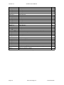
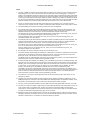
List of Figures
1:
2:
3:
4:
5:
6:
7:
8:
9:
10:
11:
12:
13:
14:
15:
16:
17:
18:
19:
20:
21:
22:
23:
24:
25:
26:
27:
28:
29:
30:
31:
32:
33:
34:
35:
36:
37:
38:
39:
40:
41:
42:
43:
44:
45:
21 October 2009
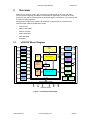
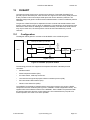
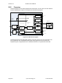
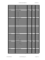
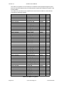
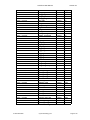
eCOG1X block diagram. . . . . . . . . . . . . . . . . . . . . . . . . . . . . . . . . . . . 2-1
Programmer’s model . . . . . . . . . . . . . . . . . . . . . . . . . . . . . . . . . . . . . . 3-2
Memory organisation . . . . . . . . . . . . . . . . . . . . . . . . . . . . . . . . . . . . . . 3-3
Example instruction sequences. . . . . . . . . . . . . . . . . . . . . . . . . . . . . 3-14
Abstract view of MMU operation.. . . . . . . . . . . . . . . . . . . . . . . . . . . . . 4-1
MMU translator blocks. . . . . . . . . . . . . . . . . . . . . . . . . . . . . . . . . . . . . 4-3
MMU reset configuration. . . . . . . . . . . . . . . . . . . . . . . . . . . . . . . . . . . 4-5
MMU example configuration.. . . . . . . . . . . . . . . . . . . . . . . . . . . . . . . . 4-6
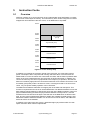
Cache memory map . . . . . . . . . . . . . . . . . . . . . . . . . . . . . . . . . . . . . . 5-1
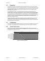
Cache tag format . . . . . . . . . . . . . . . . . . . . . . . . . . . . . . . . . . . . . . . . . 5-2
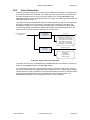
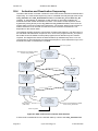
Interrupt flow diagram . . . . . . . . . . . . . . . . . . . . . . . . . . . . . . . . . . . . . 6-2
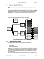
Principal modules in the eCOG1X SSM. . . . . . . . . . . . . . . . . . . . . . . . 7-1
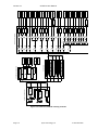
Detailed eCOG1X clocking scheme. . . . . . . . . . . . . . . . . . . . . . . . . . . 7-2
Port configuration overview . . . . . . . . . . . . . . . . . . . . . . . . . . . . . . . . . 8-1
GPIO peripheral module . . . . . . . . . . . . . . . . . . . . . . . . . . . . . . . . . . . 9-1
Connecting a 5V input signal. . . . . . . . . . . . . . . . . . . . . . . . . . . . . . . . 9-4
Connecting a 5V I/O signal . . . . . . . . . . . . . . . . . . . . . . . . . . . . . . . . . 9-4
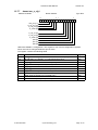
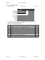
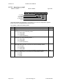
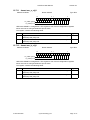
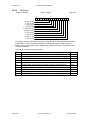
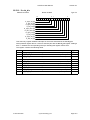
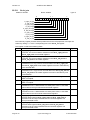
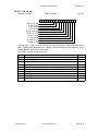
GPIO register bit fields . . . . . . . . . . . . . . . . . . . . . . . . . . . . . . . . . . . . 9-5
Parallel I/O peripheral module . . . . . . . . . . . . . . . . . . . . . . . . . . . . . . 10-1
Timer peripheral module . . . . . . . . . . . . . . . . . . . . . . . . . . . . . . . . . . 11-1
Detailed view of timers . . . . . . . . . . . . . . . . . . . . . . . . . . . . . . . . . . . 11-2
DUART peripheral module . . . . . . . . . . . . . . . . . . . . . . . . . . . . . . . . 12-1
DUART transmitter structure . . . . . . . . . . . . . . . . . . . . . . . . . . . . . . . 12-4
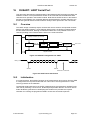
UART serial data format . . . . . . . . . . . . . . . . . . . . . . . . . . . . . . . . . . 12-4
DUART receiver structure . . . . . . . . . . . . . . . . . . . . . . . . . . . . . . . . . 12-5
DUSART peripheral module . . . . . . . . . . . . . . . . . . . . . . . . . . . . . . . 13-1
DUSART overall configuration. . . . . . . . . . . . . . . . . . . . . . . . . . . . . . 13-2
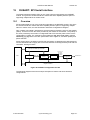
DUSART configuration for I2C . . . . . . . . . . . . . . . . . . . . . . . . . . . . . 14-1
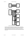
DUSART configuration for SPI . . . . . . . . . . . . . . . . . . . . . . . . . . . . . 15-1
SPI master and slave configurations . . . . . . . . . . . . . . . . . . . . . . . . . 15-2
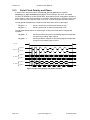
SPI clock polarity and phase selection . . . . . . . . . . . . . . . . . . . . . . . 15-4
DUSART configuration for UART . . . . . . . . . . . . . . . . . . . . . . . . . . . 16-1
UART serial data format . . . . . . . . . . . . . . . . . . . . . . . . . . . . . . . . . . 16-1
DUSART configuration for Smart Card Interface. . . . . . . . . . . . . . . . 17-1
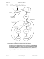
SCI control finite state machine. . . . . . . . . . . . . . . . . . . . . . . . . . . . . 17-2
DUSART configuration for Infra-Red Interface . . . . . . . . . . . . . . . . . 18-1
Generic IFR frame format . . . . . . . . . . . . . . . . . . . . . . . . . . . . . . . . . 18-2
DUSART configuration for User Serial Port. . . . . . . . . . . . . . . . . . . . 19-1
External Memory Interface peripheral module. . . . . . . . . . . . . . . . . . 20-1
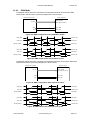
Using 8 bit memory with /RS and /WS . . . . . . . . . . . . . . . . . . . . . . . 20-5
Using 8 bit memory with R/W and /DS . . . . . . . . . . . . . . . . . . . . . . . 20-6
Using 16-bit memory with /RS and /WS . . . . . . . . . . . . . . . . . . . . . . 20-7
Using 16-bit memory with R/W and /DS . . . . . . . . . . . . . . . . . . . . . . 20-8
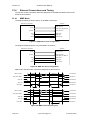
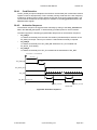
Read cycle timing diagram: 8 bit data with /RS and /WS . . . . . . . . 20-10
Write cycle timing diagram: 8 bit data with /RS and /WS . . . . . . . . 20-10
Cyan Technology Ltd
Page xiii