1
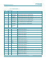
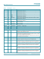
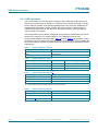
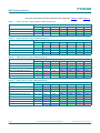
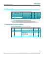
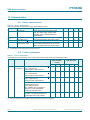
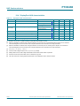
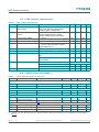
PTN3460 NXP Semiconductors eDP to LVDS bridge IC 10. Limiting values Table 14. Limiting values In accordance with the Absolute Maximum Rating System (IEC 60134). Symbol Parameter VDD supply voltage VI input voltage Tstg storage temperature VESD Conditions electrostatic discharge voltage Min Max Unit [1] 0.3 +4.6 V 3.3 V CMOS inputs [1] 0.3 VDD + 0.5 V 65 +150 C HBM [2] - 8000 V CDM [3] - 1000 V [1] All voltage values, except differential voltages, are with respect to network ground terminal. [2] Human Body Model: ANSI/EOS/ESD-S5.1-1994, standard for ESD sensitivity testing, Human Body Model – Component level; Electrostatic Discharge Association, Rome, NY, USA. [3] Charged-Device Model: ANSI/EOS/ESD-S5.3-1-1999, standard for ESD sensitivity testing, Charged-Device Model – Component level; Electrostatic Discharge Association, Rome, NY, USA. 11. Recommended operating conditions Table 15. Operating conditions Over operating free-air temperature range, unless otherwise noted. Symbol Parameter Min Typ Max Unit VDD(3V3) supply voltage (3.3 V) 3.0 3.3 3.6 V VDD(1V8) supply voltage (1.8 V) 1.7 1.8 1.9 V VI input voltage 3.3 V CMOS inputs 0 3.3 3.6 V open-drain I/O with respect to ground (e.g., DDC_SCL, DDC_SDA, MS_SDA, MS_SCL) 0 5 5.5 V operating in free air 0 - 70 C Tamb PTN3460 Product data sheet Conditions ambient temperature All information provided in this document is subject to legal disclaimers. Rev. 4 — 12 March 2014 © NXP Semiconductors N.V. 2014. All rights reserved. 19 of 32