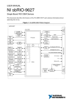
1
BT700 Qseven Board User’s Manual A31430532 1 Chapter 1 Introduction www.dfi.com Copyright FCC and DOC Statement on Class B This publication contains information that is protected by copyright. No part of it may be reproduced in any form or by any means or used to make any transformation/adaptation without the prior written permission from the copyright holders. This equipment has been tested and found to comply with the limits for a Class B digital device, pursuant to Part 15 of the FCC rules. These limits are designed to provide reasonable protection against harmful interference when the equipment is operated in a residential installation. This equipment generates, uses and can radiate radio frequency energy and, if not installed and used in accordance with the instruction manual, may cause harmful interference to radio communications. However, there is no guarantee that interference will not occur in a particular installation. If this equipment does cause harmful interference to radio or television reception, which can be determined by turning the equipment off and on, the user is encouraged to try to correct the interference by one or more of the following measures: This publication is provided for informational purposes only. The manufacturer makes no representations or warranties with respect to the contents or use of this manual and specifically disclaims any express or implied warranties of merchantability or fitness for any particular purpose. The user will assume the entire risk of the use or the results of the use of this document. Further, the manufacturer reserves the right to revise this publication and make changes to its contents at any time, without obligation to notify any person or entity of such revisions or changes. • • • Changes after the publication’s first release will be based on the product’s revision. The website will always provide the most updated information. • Reorient or relocate the receiving antenna. Increase the separation between the equipment and the receiver. Connect the equipment into an outlet on a circuit different from that to which the receiver is connected. Consult the dealer or an experienced radio TV technician for help. © 2015. All Rights Reserved. Notice: Trademarks 1. The changes or modifications not expressly approved by the party responsible for compliance could void the user’s authority to operate the equipment. 2. Shielded interface cables must be used in order to comply with the emission limits. Product names or trademarks appearing in this manual are for identification purpose only and are the properties of the respective owners. Qseven Specification Reference http://www.qseven-standard.org/ 2 Chapter 1 Introduction www.dfi.com Table of Contents Boot........................................................................................................... 32 Save & Exit ................................................................................................ 33 Updating the BIOS .................................................................................... 33 Notice: BIOS SPI ROM ............................................................................. 34 Copyright........................................................................................................... ..2 Chapter 4 - Supported Software Trademarks ........................................................................................................ 2 .......................................................... 35 Appendix A - System Error Message ................................................... 50 FCC and DOC Statement on Class B ..................................................... 2 Appendix B - Troubleshooting ................................................................ 51 About this Manual .......................................................................................... 4 Warranty ............................................................................................................ 4 Static Electricity Precautions...................................................................... 4 Safety Measures .............................................................................................. 4 About the Package ......................................................................................... 5 Chapter 1 - Introduction ............................................................................. 6 Specifications ................................................................................................ 6 Features .......................................................................................................... 7 Chapter 2 - Hardware Installation................................................ 8 Board Layout ................................................................................................. 8 Block Diagram ............................................................................................... 8 Mechanical Diagram .................................................................................... 9 System Memory .......................................................................................... 10 Cooling Option ............................................................................................ 10 MXM Connector .......................................................................................... 11 MXM Connector Signal Description ....................................................... 13 Installing BT700 onto a Carrier Board ................................................. 18 Chapter 3 - BIOS Setup ............................................................... 19 Overview ..................................................................................................... 19 AMI BIOS Setup Utility ............................................................................. 20 Main .......................................................................................................... 20 Advanced ................................................................................................... 20 Chipset ...................................................................................................... 27 Security...................................................................................................... 32 3 Chapter 1 Introduction www.dfi.com About this Manual Static Electricity Precautions An electronic file of this manual is included in the CD. To view the user’s manual in the CD, insert the CD into a CD-ROM drive. The autorun screen (Main Board Utility CD) will appear. Click “User’s Manual” on the main menu. It is quite easy to inadvertently damage your PC, system board, components or devices even before installing them in your system unit. Static electrical discharge can damage computer components without causing any signs of physical damage. You must take extra care in handling them to ensure against electrostatic build-up. 1. To prevent electrostatic build-up, leave the system board in its anti-static bag until you are ready to install it. Warranty 2. Wear an antistatic wrist strap. 1. Warranty does not cover damages or failures that arised from misuse of the product, inability to use the product, unauthorized replacement or alteration of components and product specifications. 3. Do all preparation work on a static-free surface. 4. Hold the device only by its edges. Be careful not to touch any of the components, contacts or connections. 2. The warranty is void if the product has been subjected to physical abuse, improper installation, modification, accidents or unauthorized repair of the product. 5. Avoid touching the pins or contacts on all modules and connectors. Hold modules or connectors by their ends. 3. Unless otherwise instructed in this user’s manual, the user may not, under any circumstances, attempt to perform service, adjustments or repairs on the product, whether in or out of warranty. It must be returned to the purchase point, factory or authorized service agency for all such work. Important: Electrostatic discharge (ESD) can damage your processor, disk drive and other components. Perform the upgrade instruction procedures described at an ESD workstation only. If such a station is not available, you can provide some ESD protection by wearing an antistatic wrist strap and attaching it to a metal part of the system chassis. If a wrist strap is unavailable, establish and maintain contact with the system chassis throughout any procedures requiring ESD protection. 4. We will not be liable for any indirect, special, incidental or consequencial damages to the product that has been modified or altered. Safety Measures To avoid damage to the system: • Use the correct AC input voltage range. To reduce the risk of electric shock: • Unplug the power cord before removing the system chassis cover for installation or servicing. After installation or servicing, cover the system chassis before plugging the power cord. 4 Chapter 1 Introduction www.dfi.com About the Package The package contains the following items. If any of these items are missing or damaged, please contact your dealer or sales representative for assistance. • • • • One One One One BT700 board DVD QR (Quick Reference) Heat sink Optional Items • • • • Q7X-151 carrier board kit Heat spreader Heat spreader with heat sink bracket The board and accessories in the package may not come similar to the information listed above. This may differ in accordance with the sales region or models in which it was sold. For more information about the standard package in your region, please contact your dealer or sales representative. 5 Chapter 1 Introduction www.dfi.com Chapter 1 Chapter 1 - Introduction Specifications Processor • Intel® AtomTM processors - E45: Intel® AtomTM E3845, Quad Core, 2M Cache, 1.91GHz, 10W - E26: Intel® AtomTM E3826, Dual Core, 1M Cache, 1.46GHz, 7W - E15: Intel® AtomTM E3815, Single Core, 0.5M Cache, 1.46GHz, 5W • BGA 1170 packaging technology • 22nm process technology Expansion Interfaces • Supports 1 USB 3.0 port and 1 USB HSIC for 2 USB 2.0 (default); or 4 USB 2.0 ports* (BOM option) • Supports 4 USB 2.0 ports • Supports 3 PCIe x1 (default); or 1 PCIe x4 (PCIe port 3, by default, is shared with the onboard LAN)* • Supports LPC interface • Supports I2C interface • Supports SMBus interface • Suppotrs 1 UART interface (TX/RX/CTS/RTS) Damage Free Intelligence • • • • BIOS • AMI BIOS - 64Mbit SPI BIOS Power • Input: VCC_RTC, 5V standby, 5V Power Consumption • BT700-T44-E45: 12.72W with E3845 at 1.91GHz and 4GB DDR3L memory down OS Support • • • • • • Temperature • Operating : 0oC to 60oC - Atom (Fanless) : -20oC to 70oC - Atom (Fanless with air flow) : -40oC to 85oC - Atom (Fanless with air flow) • Storage: -40oC to 85oC Humidity • 5% to 90% PCB • Dimensions - Qseven form factor - 70mm (2.76") x 70mm (2.76") • Compliance - Qseven specification revision 2.0 System Memory • 2GB/4GB DDR3L memory down • Supports DDR3L 1333MHz (-E45) Supports DDR3L 1066MHz (-E26/-E15) • Supports single channel memory interface Graphics • • • • • • • Intel® HD Graphics Supports LVDS and DDI interfaces LVDS: NXP PTN3460, 24-bit, dual channel, resolution up to 1920x1200 @60Hz Digital Display Interfaces: HDMI, DVI and DP HDMI, DVI: resolution up to 1920x1080 @60Hz DP: resolution up to 2560x1600 @60Hz Supports hardware acceleration for DirectX 11, OCL 1.2, OGL 4.0, H.264, MPEG2, MVC, VC-1, WMV9 and VP8 (supported version dependent on OS) Audio • Supports High Definition Audio interface LAN • Intel® I210AT/IT Gigabit Ethernet Controller - Intel® I210IT supports wide temperature (-40oC to 85oC) • Integrated 10/100/1000 transceiver • Fully compliant with IEEE 802.3, IEEE 802.3u, IEEE 802.3ab Serial ATA • Supports 2 Serial ATA interfaces • SATA 2.0 with data transfer rate up to 3Gb/s • Integrated Advanced Host Controller Interface (AHCI) controller eMMC* (optional) • Supports 4GB, 8GB, 16GB and 32GB eMMC onboard SD Interface • Supports 1 SD interface • Supports SDIO specification Ver. 3.0, HC Standard specification Ver. 3.0, physical layer specification Ver. 3.0, security specification Ver. 1.01 • Supports Windows 8.1 only Trusted Platform Module - TPM* (optional) • Provides a Trusted PC for secure transactions • Provides software license protection, enforcement and password protection Watchdog Timer • Watchdog timeout programmable via software from 1 to 255 seconds Monitors CPU temperature Monitors system fan speed Monitors Vcore/VGFX/VSM voltages Watchdog timer function Windows Windows Windows Windows Windows Windows 7 Ultimate x86 & SP1 (32-bit) 7 Ultimate x64 & SP1 (64-bit) 8 Enterprise x86 (32-bit) 8 Enterprise x64 (64-bit) 8.1 Enterprise x86 (32-bit) 8.1 Enterprise x64 (64-bit) Note: *Optional and is not supported in standard model. Please contact your sales representative for more information. 6 Chapter 1 Introduction www.dfi.com Chapter 1 Specification Comparison Table Features The table below shows the Qseven standard specifications and the corresponding specifications supported on the BT700 module. • DDR3L System I/O Interface DDR3L is a higher performance DDR3 SDRAM interface providing less voltage and higher speed successor. DDR3L supporting 1066MHz (-E26/-E15) or 1333MHz (-E45) delivers increased system bandwidth and improved performance to provide its higher bandwidth and its increase in performance at a lower power than DDR3 and DDR2. • Graphics The integrated Intel® HD graphics engine delivers an excellent blend of graphics performance and features to meet business needs. It provides excellent video and 3D graphics with outstanding graphics responsiveness. These enhancements deliver the performance and compatibility needed for today’s and tomorrow’s business applications. Supports HDMI, DVI and DP interfaces for display outputs. • Serial ATA Serial ATA is a storage interface that is compliant with SATA 2.0a specification. With speed of up to 3Gb/s (SATA 2.0), it improves hard drive performance faster than the standard parallel ATA whose data transfer rate is 100MB/s. • Gigabit LAN The Intel® I210AT/IT Gigabit Ethernet Controller supports up to 1Gbps data transmission. • Watchdog Timer The Watchdog Timer function allows your application to regularly “clear” the system at the set time interval. If the system hangs or fails to function, it will reset at the set time interval so that your system will continue to operate. ARM/RISC Based Minimum Configuration X86 Based Minimum Configuration Maximum Configuration DFI BT700 Configuration 3+1(shared with Ethernet) 2 6+2(shared with 1 USB 3.0 port) - BOM option 1 PCI Express Lanes 0 1 (x1 link) 4 Serial ATA channels 0 0 2 USB 2.0 ports 3 4 8 USB 3.0 ports LVDS channels embedded Display Port DisplayPort, TMDS High Definition Audio/AC'97/I2S Ethernet 10/100 Mbit/Gigabit UART Low Pin Count bus Secure Digital I/O 8-bit for SD/MMC cards System Management I2C Bus SPI Bus CAN Bus Watchdog Trigger Power Button Power Good Reset Button LID Button Sleep Button Suspend To RAM (S3 mode) Wake Battery low alarm Thermal control FAN control 0 0 2 0 0 Dual Channel 24bits Dual Channel 24bits 0 0 1 1 0 0 1 1 0 0 1 (Gigabit Ethernet) 1 0 0 0 0 1 1 1 1 0 0 1 1 0 1 0 0 1 1 1 1 0 0 1 1 0 0 1 1 1 1 0 0 1 1 1 1 1 1 1 1 1 1 1 1 1 0 1 1 1 1 1 1 0 0 1 1 0 0 0 0 0 0 0 0 1 1 1 1 1 1 1 1 7 Chapter 1 Introduction www.dfi.com Chapter 2 Chapter 2 - Hardware Installation Block Diagram Board Layout LVDS Intel Atom NXP PTN3460 HDA 2GB/4GB DDR3L memory down LPC DDR3 1333MHz Single Channel SM Bus Top View DDR3L PCIe x1 3x Switch E3800 Series AMXM Golden Finger DDR3L SPI Flash BIOS DDR3L eDP DDI IDT P9145 DDR3L PTN3460 DDR3L DDR3L SPI Flash 64Mbit Atom E3800 Series SD 2 I C Bus UART eMMC eMMC (optional) SATA 2.0 2x USB 2.0 4x DDR3L USB 3.0 1x USB 2.0 2x (Opt. share with USB 3.0) DDR3L SMSC USB4604 USB 2.0 2x USB HSIC GbE GLAN I210 Bottom View USB HSIC PCIe x1 PCIe x1 (Opt.) Intel WGI210AT 8 Chapter 2 Hardware Installation www.dfi.com Chapter 2 Mechanical Diagram BT700 Module BT700 Module with thermal solution 70.00 66.99 66.05 11.52 2.99 64.90 3.95 20.00 70.00 64.90 56.50 70.00 56.50 Top View 0.00 0.00 Module PCB 1.20 6.00 14.00 11.53 20.00 Heatsink Bottom View Side View of the Module with thermal solution and Carrier Board 00.0 00.0 9 Chapter 2 Hardware Installation www.dfi.com Chapter 2 Cooling Option Important: Electrostatic discharge (ESD) can damage your processor, disk drive and other components. Perform the upgrade instruction procedures described at an ESD workstation only. If such a station is not available, you can provide some ESD protection by wearing an antistatic wrist strap and attaching it to a metal part of the system chassis. If a wrist strap is unavailable, establish and maintain contact with the system chassis throughout any procedures requiring ESD protection. Heat Spreader with Heat Sink System Memory The system board is equipped with eight 2GB/4GB DDR3L onboard memory inerfaces. • Supports DDR3L 1333MHz (-E45/-E27/-J00/-N30/-N07) Supports DDR3L 1066MHz (-E26/-E25/-E15) • Supports single channel memory interface Top View of the Heat Sink DDR3L Top View 1 2 DDR3L Bottom View of the Heat Sink Bottom View • “1” and “2“ denote the locations of the thermal pads designed to contact the corresponding components that are on BT700. • Remove the plastic covering from the thermal pads prior to mounting the heat sink onto BT700. 10 Chapter 2 Hardware Installation www.dfi.com Chapter 2 MXM Connector MXM Connector The MXM connector is used to interface with the carrier board. Insert BT700 to the MXM connector on the carrier board. Refer to the following pages for the pin functions of this connector. Refer to “Installing BT700 onto a Carrier Board” section for more information. 11 Chapter 2 Hardware Installation www.dfi.com Chapter 2 Pin 1 3 5 7 9 11 13 15 17 19 21 23 25 27 29 31 33 35 37 39 41 43 45 47 49 51 53 55 57 59 61 63 65 67 69 71 73 75 77 79 81 83 85 87 89 91 93 95 97 99 101 103 105 107 109 111 113 115 Q7 R2.0 Signal GND GBE_MDI3GBE_MDI3+ GBE_LINK100# GBE_MDI1GBE_MDI1+ GBE_LINK# GBE_CTREF WAKE# SUS_STAT# SLP_BTN# GND KEY GND BATLOW# SATA0_TX+ SATA0_TXSATA_ACT# SATA0_RX+ SATA0_RXGND BIOS_DISABLE# / BOOT_ALT# SDIO_CD# SDIO_CMD SDIO_PWR# SDIO_DAT0 SDIO_DAT2 SDIO_DAT4 SDIO_DAT6 GND HDA_SYNC / I2S_WS HDA_RST# / I2S_RST# HDA_BITCLK / I2S_CLK HDA_SDI / I2S_SDI HDA_SDO / I2S_SDO THRM# THRMTRIP# GND USB_P7- / USB_SSTX0USB_P7+ / USB_SSTX0+ USB_6_7_OC# USB_P5- / USB_SSTX1USB_P5+ / USB_SSTX1+ USB_2_3_OC# USB_P3USB_P3+ USB_CC USB_P1USB_P1+ GND eDP0_TX0+ / LVDS_A0+ eDP0_TX0- / LVDS_A0eDP0_TX1+ / LVDS_A1+ eDP0_TX1- / LVDS_A1eDP0_TX2+ / LVDS_A2+ eDP0_TX2- / LVDS_A2LVDS_PPEN eDP0_TX3+ / LVDS_A3+ eDP0_TX3- / LVDS_A3- BT700 Signal GND GBE_MDI3GBE_MDI3+ GBE_LINK100# GBE_MDI1GBE_MDI1+ NC NC WAKE# SUS_STAT# SLP_BTN# GND KEY GND BATLOW# SATA0_TX+ SATA0_TXSATA_ACT# SATA0_RX+ SATA0_RXGND BIOS_DISABLE# SDIO_CD# SDIO_CMD SDIO_PWR# SDIO_DAT0 SDIO_DAT2 NC NC GND HDA_SYNC HDA_RST# HDA_BITCLK HDA_SDI HDA_SDO THRM# THRMTRIP# GND USB_SSTX0USB_SSTX0+ USB_6_7_OC# USB_P5USB_P5+ USB_2_3_OC# USB_P3USB_P3+ NC USB_P1USB_P1+ GND LVDS_A0+ LVDS_A0LVDS_A1+ LVDS_A1LVDS_A2+ LVDS_A2LVDS_PPEN LVDS_A3+ LVDS_A3- Pin 2 4 6 8 10 12 14 16 18 20 22 24 26 28 30 32 34 36 38 40 42 44 46 48 50 52 54 56 58 60 62 64 66 68 70 72 74 76 78 80 82 84 86 88 90 92 94 96 98 100 102 104 106 108 110 112 114 116 Q7 R2.0 Signal GND GBE_MDI2GBE_MDI2+ GBE_LINK1000# GBE_MDI0GBE_MDI0+ GBE_ACT# SUS_S5# SUS_S3# PWRBTN# LID_BTN# GND KEY PWGIN RSTBTN# SATA1_TX+ SATA1_TXGND SATA1_RX+ SATA1_RXGND SDIO_CLK# SDIO_LED SDIO_WP SDIO_DAT1 SDIO_DAT3 SDIO_DAT5 SDIO_DAT7 RSVD GND SMB_CLK / GP1_I2C_CLK SMB_DAT / GP1_I2C_DAT SMB_ALERT# GP0_I2C_CLK GP0_I2C_DAT WDTRIG# WDOUT GND USB_P6- / USB_SSRX0USB_P6+ / USB_SSRX0+ USB_4_5_OC# USB_P4- / USB_SSRX1USB_P4+ / USB_SSRX1+ USB_0_1_OC# USB_P2USB_P2+ USB_ID USB_P0USB_P0+ GND eDP1_TX0+ / LVDS_B0+ eDP1_TX0- / LVDS_B0eDP1_TX1+ / LVDS_B1+ eDP1_TX1- / LVDS_B1eDP1_TX2+ / LVDS_B2+ eDP1_TX2- / LVDS_B2LVDS_BLEN eDP1_TX3+ / LVDS_B3+ eDP1_TX3- / LVDS_B3- BT700 Signal GND GBE_MDI2GBE_MDI2+ GBE_LINK1000# GBE_MDI0GBE_MDI0+ GBE_ACT# SUS_S4# SUS_S3# PWRBTN# LID_BTN# GND KEY PWGIN RSTBTN# SATA1_TX+ SATA1_TXGND SATA1_RX+ SATA1_RXGND SDIO_CLK# NC SDIO_WP SDIO_DAT1 SDIO_DAT3 NC NC NC GND SMB_CLK SMB_DAT SMB_ALERT# GP0_I2C_CLK GP0_I2C_DAT WDTRIG# WDOUT GND USB_SSRX0USB_SSRX0+ USB_4_5_OC# USB_P4USB_P4+ USB_0_1_OC# USB_P2USB_P2+ NC USB_P0USB_P0+ GND LVDS_B0+ LVDS_B0LVDS_B1+ LVDS_B1LVDS_B2+ LVDS_B2LVDS_BLEN LVDS_B3+ LVDS_B3- Pin 117 119 121 123 125 127 129 131 133 135 137 139 141 143 145 147 149 151 153 155 157 159 161 163 165 167 169 171 173 175 177 179 181 183 185 187 189 191 193 195 197 199 201 203 205 207 209 211 213 215 217 219 221 223 225 227 229 Q7 R2.0 Signal GND eDP0_AUX+ / LVDS_A_CLK+ eDP0_AUX- / LVDS_A_CLKLVDS_BLT_CTRL /GP_PWM_OUT0 GP2_I2C_DAT / LVDS_DID_DAT GP2_I2C_CLK / LVDS_DID_CLK CAN0_TX DP_LANE3+ / TMDS_CLK+ DP_LANE3- / TMDS_CLKGND DP_LANE1+ / TMDS_LANE1+ DP_LANE1- / TMDS_LANE1GND DP_LANE2+ / TMDS_LANE0+ DP_LANE2- / TMDS_LANE0GND DP_LANE0+ / TMDS_LANE2+ DP_LANE0- / TMDS_LANE2DP_HDMI_HPD# PCIE_CLK_REF+ PCIE_CLK_REFGND PCIE3_TX+ PCIE3_TXGND PCIE2_TX+ PCIE2_TXUART0_TX PCIE1_TX+ PCIE1_TXUART0_RX PCIE0_TX+ PCIE0_TXGND LPC_AD0 / GPIO0 LPC_AD2 / GPIO2 LPC_CLK / GPIO4 SERIRQ / GPIO6 VCC_RTC FAN_TACHOIN / GP_TIMER_IN GND SPI_MOSI SPI_MISO SPI_SCK VCC_5V_SB MFG_NC0 MFG_NC1 VCC VCC VCC VCC VCC VCC VCC VCC VCC VCC BT700 Signal GND LVDS_A_CLK+ LVDS_A_CLKLVDS_BLT_CTRL LVDS_DID_DAT LVDS_DID_CLK NC DP_LANE3+ DP_LANE3GND DP_LANE1+ DP_LANE1GND DP_LANE2+ DP_LANE2GND DP_LANE0+ DP_LANE0DP_HDMI_HPD# PCIE_CLK_REF+ PCIE_CLK_REFGND NC NC GND PCIE2_TX+ PCIE2_TXUART0_TX PCIE1_TX+ PCIE1_TXUART0_RX PCIE0_TX+ PCIE0_TXGND LPC_AD0 LPC_AD2 LPC_CLK SERIRQ VCC_RTC FAN_TACHOIN GND SPI_MOSI SPI_MISO SPI_SCK VCC_5V_SB NC UART1_TX VCC VCC VCC VCC VCC VCC VCC VCC VCC VCC Pin 118 120 122 124 126 128 130 132 134 136 138 140 142 144 146 148 150 152 154 156 158 160 162 164 166 168 170 172 174 176 178 180 182 184 186 188 190 192 194 196 198 200 202 204 206 208 210 212 214 216 218 220 222 224 226 228 230 Q7 R2.0 Signal GND eDP1_AUX+ / LVDS_B_CLK+ eDP1_AUX- / LVDS_B_CLKGP_1-Wire_Bus eDP0_HPD# / LVDS_BLC_DAT eDP1_HPD# / LVDS_BLC_CLK CAN0_RX RSVD (Differential Pair) RSVD (Differential Pair) GND DP_AUX+ DP_AUXGND RSVD (Differential Pair) RSVD (Differential Pair) GND HDMI_CTRL_DAT HDMI_CTRL_CLK RSVD PCIE_WAKE# PCIE_RST# GND PCIE3_RX+ PCIE3_RXGND PCIE2_RX+ PCIE2_RXUART0_RTS# PCIE1_RX+ PCIE1_RXUART0_CTS# PCIE0_RX+ PCIE0_RXGND LPC_AD1 / GPIO1 LPC_AD3 / GPIO3 LPC_FRAME# / GPIO5 LPC_LDRQ# / GPIO7 SPKR / GP_PWM_OUT2 FAN_PWMOUT / GP_PWM_OUT1 GND SPI_CS0# SPI_CS1# MFG_NC4 VCC_5V_SB MFG_NC2 MFG_NC3 VCC VCC VCC VCC VCC VCC VCC VCC VCC VCC BT700 Signal GND LVDS_B_CLK+ LVDS_B_CLKGP_1-Wire_Bus NC NC NC NC NC GND DP_AUX+ DP_AUXGND NC NC GND HDMI_CTRL_DAT HDMI_CTRL_CLK NC PCIE_WAKE# PCIE_RST# GND NC NC GND PCIE2_RX+ PCIE2_RXUART0_RTS# PCIE1_RX+ PCIE1_RXUART0_CTS# PCIE0_RX+ PCIE0_RXGND LPC_AD1 LPC_AD3 LPC_FRAME# NC SPKR FAN_PWMOUT GND SPI_CS0# NC NC VCC_5V_SB UART1_RX NC VCC VCC VCC VCC VCC VCC VCC VCC VCC VCC 12 Chapter 2 Hardware Installation www.dfi.com Chapter 2 MXM Connector Signal Description Pin Types I Input Pin O Output Pin I/O Bi-directional input / output Pin OD Open drain OC Open Collector PP Push Pull NC Not Connected PCI Express Interface Signals Descriptions Signal Pin# PCIE0_RX+ 180 PCIE0_RX182 PCIE0_TX+ 179 PCIE0_TXPCIE1_RX+ PCIE1_RX- 181 PCIE1_TX+ 173 PCIE1_TXPCIE2_RX+ PCIE2_RX- 175 PCIE2_TX+ 174 176 168 170 167 169 Pin Type Pwr Rail /Tolerance I PCIE PCIE O PCIE PCIE I PCIE PCIE O PCIE PCIE I PCIE PCIE O PCIE PCIE I PCIE PCIE O PCIE PCIE O PCIE PCIE BT700 AC Coupling capacitor AC Coupling capacitor AC Coupling capacitor AC Coupling capacitor AC Coupling capacitor AC Coupling capacitor Carrier Board Description Device - Connect AC Coupling cap 0.1uF Slot - Connect to PCIE Conn pin PCI Express channel 0, Receive Input differential pair. Connect to PCIE device or slot PCI Express channel 0, Transmit Output differential pair. Device - Connect AC Coupling cap 0.1uF Slot - Connect to PCIE Conn pin PCI Express channel 1, Receive Input differential pair. Connect to PCIE device or slot PCI Express channel 1, Transmit Output differential pair. Device - Connect AC Coupling cap 0.1uF Slot - Connect to PCIE Conn pin PCI Express channel 2, Receive Input differential pair. Connect to PCIE device or slot PCI Express channel 2, Transmit Output differential pair. Device - Connect AC Coupling cap 0.1uF (This Port is BOM Option with On board LAN) Slot - Connect to PCIE Conn pin PCI Express channel 3, Receive Input differential pair.(This Port is BOM Option with On board LAN) PCIE2_TXPCIE3_RX+ PCIE3_RXPCIE3_TX+ PCIE3_TXPCIE_CLK_REF+ PCIE_CLK_REF- 162 164 161 163 155 157 PCIE_WAKE# 156 I CMOS 3.3V Suspend/3.3V PCIE_RST# 158 O CMOS 3.3V/3.3V UART Interface Signals Signal Pin# Pin Type Pwr Rail /Tolerance UART0_TX 171 O CMOS 3.3V/3.3V Connect to UART device Serial Data Transmitter UART0_RX 177 I CMOS 3.3V/3.3V Connect to UART device Serial Data Reciever AC Coupling capacitor AC Coupling capacitor Connect to PCIE device or slot (This Port is BOM Option with On board LAN) PCI Express channel 3, Transmit Output differential pair.(This Port is BOM Option with On board LAN) Connect to PCIE device, PCIe CLK Buffer or slot PCI Express Reference Clock for Lanes 0 to 3. PU 10K to 3.3V Suspend PCI Express Wake Event: Sideband wake signal asserted by components requesting wakeup. Reset Signal for external devices. BT700 Carrier Board Description UART0_CTS# 178 I CMOS 3.3V/3.3V Connect to UART device Handshake signal, ready to send data UART0_RTS# 172 O CMOS 3.3V/3.3V Connect to UART device Handshake signal, ready to receive data Signal GBE_MDI0+ GBE_MDI0- Pin# 12 10 Pin Type Pwr Rail /Tolerance I/O GB_LAN GB_LAN GBE_MDI1+ GBE_MDI1GBE_MDI2+ GBE_MDI2GBE_MDI3+ 11 9 6 4 5 GBE_MDI3- 3 Gigabit Ethernet Signals BT700 Carrier Board Description Connect to Magnetics Module MDI0+/- Media Dependent Interface (MDI) differential pair 0. The MDI can operate in 1000, 100, and 10Mbit/sec modes.This signal pair is used for all modes. I/O GB_LAN GB_LAN Connect to Magnetics Module MDI1+/- Media Dependent Interface (MDI) differential pair 1. The MDI can operate in 1000, 100, and 10Mbit/sec modes.This signal pair is used for all modes. I/O GB_LAN GB_LAN Connect to Magnetics Module MDI2+/- Media Dependent Interface (MDI) differential pair 2. The MDI can operate in 1000, 100, and 10Mbit/sec modes.This signal pair is used for all modes. I/O GB_LAN GB_LAN Connect to Magnetics Module MDI3+/- Media Dependent Interface (MDI) differential pair 3. The MDI can operate in 1000, 100, and 10Mbit/sec modes.This signal pair is used for all modes. NC Reference voltage for carrier board Ethernet channel 0 magnetics center tap. The reference voltage is determined by the requirements of the module's PHY and may be as low as 0V and as high as 3.3V. The reference voltage output should be current limited on the module. In a case in which the reference is shorted to ground, the current must be limited to 250mA or less. NC Ethernet controller 0 link indicator, active low. GBE_CTREF 15 REF GBE_LINK# 13 O CMOS 3.3V PP 3.3V/3.3V GBE_LINK100# 7 O CMOS 3.3V PP 3.3V/3.3V Ethernet controller 0 100Mbit/sec link indicator, active low. GBE_LINK1000# 8 O CMOS 3.3V PP 3.3V/3.3V Ethernet controller 0 1000Mbit/sec link indicator, active low. GBE_ACT# 14 O CMOS 3.3V PP 3.3V/3.3V Ethernet controller 0 activity indicator, active low. 13 Chapter 2 Hardware Installation www.dfi.com Chapter 2 Serial ATA Interface Signals Signal SATA0_RX+ SATA0_RXSATA0_TX+ SATA0_TXSATA1_RX+ SATA1_RXSATA1_TX+ SATA1_TX- Pin# 35 37 29 31 36 38 30 32 SATA_ACT# USB Interface Signals Signal USB_P0+ USB_P0USB_P1+ USB_P1USB_P2+ USB_P2USB_P3+ USB_P3USB_P4+ USB_SSRX1+ USB_P4USB_SSRX1USB_P5+ USB_SSTX1+ USB_P5USB_SSTX1USB_P6+ USB_SSRX0+ USB_P6USB_SSRX0USB_P7+ USB_SSTX0+ USB_P7USB_SSTX0USB_0_1_OC# Pin Type Pwr Rail /Tolerance I SATA SATA O SATA SATA I SATA SATA O SATA SATA 33 O OC 3.3V 3.3V/3.3V Pin# 96 94 95 93 90 88 89 87 Pin Type Pwr Rail /Tolerance I/O USB USB I/O USB USB I/O USB USB I/O USB USB I/O USB I USB USB Connect 90 ಳ @100MHz Common Choke in series and ESD suppressors to GND to USB connector Universal Serial Bus Port 4 differential pair. Multiplexed with receive signal differential pairs for the Superspeed USB data path. I/O USB O USB USB Connect 90 ಳ @100MHz Common Choke in series and ESD suppressors to GND to USB connector Universal Serial Bus Port 5 differential pair. Multiplexed with transmit signal differential pairs for the Superspeed USB data path. I/O USB I USB USB 84 82 83 81 78 76 77 75 AC AC AC AC AC AC AC AC BT700 Coupling capacitor Coupling capacitor Coupling capacitor Coupling capacitor Coupling capacitor Coupling capacitor Coupling capacitor Coupling capacitor USB Description Serial ATA channel 0, Receive Input differential pair. Connect to SATA0 Conn TX pin Serial ATA channel 0, Transmit Output differential pair. Connect to SATA1 Conn RX pin Serial ATA channel 1, Receive Input differential pair. Connect to SATA1 Conn TX pin Serial ATA channel 1, Transmit Output differential pair. Serial ATA Led. Open collector output pin driven during SATA command activity. BT700 Carrier Board Connect 90 ಳ @100MHz Common Choke in series and ESD suppressors to GND to connector Connect 90 ಳ @100MHz Common Choke in series and ESD suppressors to GND to connector Connect 90 ಳ @100MHz Common Choke in series and ESD suppressors to GND to connector Connect 90 ಳ @100MHz Common Choke in series and ESD suppressors to GND to connector Description USB USB USB USB Universal Serial Bus Port 0 differential pair. Universal Serial Bus Port 1 differential pair.This port may be optionally used as USB client port. Universal Serial Bus Port 2 differential pair. Universal Serial Bus Port 3 differential pair. Universal Serial Bus Port 6 differential pair. Multiplexed with receive signal differential pairs for the Superspeed USB data path. AC Coupling capacitor I/O USB O USB Carrier Board Connect to SATA0 Conn RX pin Connect Common Choke in series and ESD suppressors to GND to USB connector(This Port is BOM Option with USB_P6 / USB_P7) Universal Serial Bus Port 7 differential pair. Multiplexed with transmit signal differential pairs for the Superspeed USB data path. AC Coupling capacitor 86 I CMOS 3.3V Suspend/3.3V PU 10K to 3.3V Suspend Connect to Overcurrent of USB Power Switch Over current detect input 1. This pin is used to monitor the USB power over current of the USB Ports 0 and 1. USB_2_3_OC# 85 I CMOS 3.3V Suspend/3.3V PU 10K to 3.3V Suspend Connect to Overcurrent of USB Power Switch Over current detect input 2. This pin is used to monitor the USB power over current of the USB Ports 2 and 3. USB_4_5_OC# USB_6_7_OC# 80 79 I CMOS I CMOS 3.3V Suspend/3.3V 3.3V Suspend/3.3V PU 10K to 3.3V Suspend PU 10K to 3.3V Suspend Connect to Overcurrent of USB Power Switch Connect to Overcurrent of USB Power Switch USB_ID 92 I CMOS 3.3V Suspend/3.3V NC Over current detect input 3. This pin is used to monitor the USB power over current of the USB Ports 4 and 5. Over current detect input 4. This pin is used to monitor the USB power over current of the USB Ports 6 and 7. USB ID pin.Configures the mode of the USB Port 1. If the signal is detected as being 'high active' the BIOS will automatically configure USB Port 1 as USB Client and enable USB Client support. This signal should be driven as OC signal by external circuitry. USB_CC 91 I CMOS 3.3V Suspend/3.3V NC Signal Pin# Pin Type Pwr Rail /Tolerance SDIO_CD# 43 I/O CMOS 3.3V/3.3V Connect to SD Card SDIO Card Detect. This signal indicates when a SDIO/MMC card is present. SDIO_CLK 42 O CMOS 3.3V/3.3V Connect to SD Card SDIO_CMD 45 I/O OD/PP CMOS 3.3V/3.3V SDIO Clock. With each cycle of this signal a one-bit transfer on the command and each data line occurs. This signal has maximum frequency of 48 MHz. SDIO Command/Response. This signal is used for card initialization and for command transfers. During initialization mode this signal is open drain. During command transfer this signal is in push-pull mode. SDIO_LED SDIO_WP SDIO_PWR# SDIO_DAT0-7 44 46 47 48-55 O CMOS I/O CMOS O CMOS I/O PP CMOS 3.3V/3.3V 3.3V/3.3V 3.3V/3.3V 3.3V/3.3V USB Client Connect pin.If USB Port 1 is configured for client mode then an externally connected USB host should set this signal to high-active in order to properly make the connection with the module's internal USB client controller. If the external USB host is disconnected, this signal should be set to low-active in order to inform the USB client controller that the external host has been disconnected. A level shifter/protection circuitry should be implemented on the carrier board for this signal. SDIO Interface Signals BT700 Carrier Board Description Connect to SD Card NC SDIO SDIO SDIO SDIO Connect to SD Card SDIO_DAT4-7 NC Connect to SD Card LED. Used to drive an external LED to indicate when transfers occur on the bus. Write Protect. This signal denotes the state of the write-protect tab on SD cards. Power Enable. This signal is used to enable the power being supplied to a SD/MMC card device. Data lines. These signals operate in push-pull mode High Definition Audio Signals/AC'97 Signal HDA_RST# I2S_RST# HDA_SYNC I2S_WS HDA_BCLK I2S_CLK HDA_SDO I2S_SDO HDA_SDIN I2S_SDI Pin# Pin Type Pwr Rail /Tolerance 61 O CMOS 3.3V/3.3V BT700 Connect to CODEC Carrier Board 59 O CMOS 3.3V/3.3V Connect to CODEC 63 O CMOS 3.3V/3.3V Connect to CODEC 67 O CMOS 3.3V/3.3V Connect to CODEC 65 I CMOS 3.3V/3.3V Connect to CODEC Description HD Audio/AC'97 Codec Reset. Multiplexed with I2S Codec Reset. Serial Bus Synchronization. Multiplexed with I2S Word Select from Codec. HD Audio/AC'97 24 MHz Serial Bit Clock from Codec. Multiplexed with I2S Serial Data Clock from Codec. HD Audio/AC'97 Serial Data Output to Codec. Multiplexed with I2S Serial Data Output from Codec. HD Audio/AC'97 Serial Data input to Codec. Multiplexed with I2S Serial Data Input from Codec. 14 Chapter 2 Hardware Installation www.dfi.com Chapter 2 LVDS Flat Panel Signals Signal Pin# Pin Type Pwr Rail /Tolerance LVDS_PPEN 111 O CMOS 3.3V/3.3V Carrier Board Connect to enable control of LVDS panel power circuit LVDS_BLEN 112 O CMOS 3.3V/3.3V Connect to enable control of LVDS panel backlight power circuit. LVDS_BLT_CTRL/GP_PWM_OUT0 123 O CMOS 3.3V/3.3V LVDS_A0+ eDP0_TX0+ LVDS_A0eDP0_TX0LVDS_A1+ eDP0_TX1+ LVDS_A1eDP0_TX1LVDS_A2+ eDP0_TX2+ LVDS_A2eDP0_TX2LVDS_A3+ eDP0_TX3+ LVDS_A3eDP0_TX3LVDS_A_CLK+ eDP0_AUX+ LVDS_A_CLKeDP0_AUXLVDS_B0+ eDP1_TX0+ LVDS_B0eDP1_TX0LVDS_B1+ eDP1_TX1+ LVDS_B1eDP1_TX1LVDS_B2+ eDP1_TX2+ LVDS_B2eDP1_TX2LVDS_B3+ eDP1_TX3+ LVDS_B3eDP1_TX3LVDS_B_CLK+ eDP1_AUX+ LVDS_B_CLKeDP1_AUXLVDS_DID_CLK/GP_I2C_CLK LVDS_DID_DAT/GP_I2C_DAT LVDS_BLC_CLK/eDP1_HPD# LVDS_BLC_DAT/eDP0_HPD# BT700 Description Controls panel power enable. Connect to brightness control of LVDS panel backlight power circuit. Connect to LVDS connector 99 O LVDS LVDS O LVDS LVDS O LVDS LVDS LVDS primary channel differential pair 0. Display Port primary channel differential pair 0. 101 Connect to LVDS connector 103 LVDS primary channel differential pair 1. Display Port primary channel differential pair 1. 105 Connect to LVDS connector 107 LVDS primary channel differential pair 2. Display Port primary channel differential pair 2. 109 Connect to LVDS connector 113 O LVDS LVDS O LVDS LVDS O LVDS LVDS O LVDS LVDS O LVDS LVDS O LVDS LVDS LVDS primary channel differential pair 3. Display Port primary channel differential pair 3. 115 Connect to LVDS connector 119 LVDS primary channel differential pair clock lines. Display Port primary auxiliary channel. 121 Connect to LVDS connector 100 LVDS secondary channel differential pair 0. Display Port secondary channel differential pair 0. 102 Connect to LVDS connector 104 LVDS secondary channel differential pair 1. Display Port secondary channel differential pair 1. 106 Connect to LVDS connector 108 LVDS secondary channel differential pair 2. Display Port secondary channel differential pair 2. 110 Connect to LVDS connector 114 LVDS secondary channel differential pair 3. Display Port secondary channel differential pair 3. 112 Connect to LVDS connector 120 LVDS secondary channel differential pair clock lines. Display Port secondary auxiliary channel. LVDS O LVDS 122 127 125 128 126 DisplayPort Interface Signals Signal Pin# DP_LANE3DP_LANE3+ DP_LANE2DP_LANE2+ DP_LANE1DP_LANE1+ 133 131 145 143 139 137 DP_LANE0- 151 DP_LANE0+ 149 DP_AUXDP_AUX+ DP_HDMI_HPD# 140 138 153 Controls panel Backlight enable. Primary functionality is to control the panel backlight brightness via pulse width modulation (PWM). When not in use for this primary purpose it can be used as General Purpose PWM Output. I/O I/O I/O I/O OD OD OD OD CMOS CMOS CMOS CMOS 3.3V/3.3V 3.3V/3.3V 3.3V/3.3V 3.3V/3.3V PU 2.2K to 3.3V PU 2.2K to 3.3V NC NC Pin Type Pwr Rail /Tolerance O PCIE DP AC coupled off Module O PCIE DP AC coupled off Module O PCIE DP AC coupled off Module O PCIE DP AC coupled off Module I/O PCIE DP AC coupled off Module I CMOS 3.3V/3.3V Connect to DDC clock of LVDS panel Connect to DDC clock of LVDS panel BT700 Primary functionality is DisplayID DDC clock line used for LVDS flat panel detection. If primary functionality is not used it can be as General Purpose I²C bus clock line. Primary functionality DisplayID DDC data line used for LVDS flat panel detection. If primary functionality is not used it can be as General Purpose I²C bus data line. Control clock signal for external SSC clock chip. If the primary functionality is not used, it can be used as an embedded DisplayPort secondary Hotplug detection. Control data signal for external SSC clock chip. If the primary functionality is not used, it can be used as an embedded DisplayPort primary Hotplug detection. Carrier Board Connect Connect Connect Connect Connect Connect AC AC AC AC AC AC Coupling Coupling Coupling Coupling Coupling Coupling Capacitors Capacitors Capacitors Capacitors Capacitors Capacitors 0.1uF 0.1uF 0.1uF 0.1uF 0.1uF 0.1uF to to to to to to Description Device Device Device Device Device Device DisplayPort differential pair lines lane 3. DisplayPort differential pair lines lane 2. DisplayPort differential pair lines lane 1. Connect AC Coupling Capacitors 0.1uF to Device DisplayPort differential pair lines lane 0. Connect AC Coupling Capacitors 0.1uF to Device Connect AC Coupling Capacitors 0.1uF to Device, PU 100K to 3.3V Connect AC Coupling Capacitors 0.1uF to Device, PD 100K to GND PU 10K to 3.3V Auxiliary channel used for link management and device control. Differential pair lines. Hot plug detection signal that serves as an interrupt request. HDMI Interface Signals Signal Pin# TMDS_CLK- 133 TMDS_CLK+ 131 TMDS_LANE0- 145 Pin Type Pwr Rail /Tolerance O TMDS TMDS AC coupled off Module BT700 O TMDS TMDS AC coupled off Module O TMDS TMDS AC coupled off Module O TMDS TMDS AC coupled off Module Carrier Board Description Connect AC Coupling Capacitors 0.1uF to Device TMDS differential pair clock lines. Connect AC Coupling Capacitors 0.1uF to Device Connect AC Coupling Capacitors 0.1uF to Device TMDS differential pair lines lane 0. TMDS_LANE0+ 143 TMDS_LANE1TMDS_LANE1+ TMDS_LANE2- 139 137 151 Connect AC Coupling Capacitors 0.1uF to Device TMDS_LANE2+ 149 HDMI_CTRL_CLK 152 I/O OD CMOS 3.3V/3.3V PU 2.2K to 3.3V DDC based control signal (clock) for HDMI device. Note: Level shifters must be implemented on the carrier board for this signal in order to be compliant with the HDMI Specification. HDMI_CTRL_DAT 150 I/O OD CMOS 3.3V/3.3V PU 2.2K to 3.3V DDC based control signal (data) for HDMI device. Note: Level shifters must be implemented on the carrier board for this signal in order to be compliant with the HDMI Specification DP_HDMI_HPD# 153 I CMOS 3.3V/3.3V PU 10K to 3.3V Hot plug detection signal that serves as an interrupt request. Connect AC Coupling Capacitors 0.1uF to Device Connect AC Coupling Capacitors 0.1uF to Device Connect AC Coupling Capacitors 0.1uF to Device TMDS differential pair lines lane 1. TMDS differential pair lines lane 2. Connect AC Coupling Capacitors 0.1uF to Device 15 Chapter 2 Hardware Installation www.dfi.com Chapter 2 LPC Interface Signals Signal LPC_AD[0..3] GPIO[0..3] LPC_FRAME# GPIO5 LPC_LDRQ# GPIO7 LPC_CLK GPIO4 SERIRQ GPIO6 Pin# Pin Type Pwr Rail /Tolerance 185-188 I/O CMOS 3.3V/3.3V BT700 Carrier Board Description Multiplexed Command, Address and Data. General purpose input/output [0..3] LPC frame indicates the start of a new cycle or the termination of a broken cycle. General purpose input/output 5. LPC DMA request. General purpose input/output 7. LPC clock. General purpose input/output 4. Serialized Interrupt. General purpose input/output 6. 190 I/O CMOS 3.3V/3.3V 192 I/O CMOS 3.3V/3.3V 189 I/O CMOS 3.3V/3.3V Connect to LPC device 191 I/O CMOS 3.3V/3.3V Connect to LPC device Signal Pin# Pin Type Pwr Rail /Tolerance SPI_MOSI SPI_MISO SPI_SCK SPI_CS0# SPI_CS1# 199 201 203 200 202 O CMOS I CMOS O CMOS O CMOS O CMOS 3.3V/3.3V 3.3V/3.3V 3.3V/3.3V 3.3V/3.3V 3.3V/3.3V Carrier Board Description SPI SPI SPI SPI Master serial output/Slave serial input signal. SPI serial output data from Qseven module to the SPI device. Master serial input/Slave serial output signal. SPI serial input data from the SPI device to Qseven module. SPI clock output. SPI chip select 0 output. SPI Chip Select 1 signal is used as the second chip select when two devices are used. Do not use when only one SPI device is used. Signal Pin# Pin Type Pwr Rail /Tolerance CAN0_TX 129 O CMOS 3.3V/3.3V NC CAN (Controller Area Network) TX output for CAN Bus channel 0. In order to connect a CAN controller device to the Qseven module's CAN bus it is necessary to add transceiver hardware to the carrier board. CAN0_RX 130 I CMOS 3.3V/3.3V NC RX input for CAN Bus channel 0. In order to connect a CAN controller device to the Qseven module's CAN bus it is necessary to add transceiver hardware to the carrier board. Connect to LPC device Connect to LPC device NC SPI Interface Signals BT700 Connect Connect Connect Connect a a a a series series series series resistor resistor resistor resistor to to to to Carrier Carrier Carrier Carrier Board Board Board Board Device Device Device Device SI pin SO pin SCK pin CS# pin NC CAN Bus Interface Signals BT700 Carrier Board Description Power Control Signals Signal Pin# Pin Type Pwr Rail /Tolerance PWGIN 26 I CMOS 5V/5V PWRBTN# 20 I CMOS 3.3V Standby Power Management Signals Signal Pin# Pin Type Pwr Rail /Tolerance RSTBTN# 28 I CMOS 3.3V/3.3V BT700 Carrier Board Description PU 10K to 5V High active input for the Qseven® module indicates that all power rails located on the carrier board are ready for use. PU 10K to 3.3V Suspend BT700 Power Button: Low active power button input. This signal is triggered on the falling edge. Carrier Board Description PU 10K to 3.3V Reset button input. This input may be driven active low by an external circuitry to reset the Qseven module. BATLOW# 27 I CMOS 3.3V Suspend/3.3V PU 10K to 3.3V Suspend Battery low input. This signal may be driven active low by external circuitry to signal that the system battery is low or may be used to signal some other external battery management event. WAKE# 17 I CMOS 3.3V Suspend/3.3V PU 10K to 3.3V Suspend External system wake event. This may be driven active low by external circuitry to signal an external wake-up event. SUS_STAT# 19 O CMOS 3.3V Suspend/3.3V PU 10K to 3.3V Suspend Suspend Status: indicates that the system will be entering a low power state soon. SUS_S3# 18 O CMOS 3.3V Suspend/3.3V SUS_S5# 16 O CMOS 3.3V Suspend/3.3V SLP_BTN# 21 I CMOS 3.3V Suspend/3.3V PU 10K to 3.3V Suspend Sleep button. Low active signal used by the ACPI operating system to transition the system into sleep state or to wake it up again. This signal is triggered on falling edge. LID_BTN# 22 I CMOS 3.3V Suspend/3.3V PU 10K to 3.3V Suspend LID button. Low active signal used by the ACPI operating system to detect a LID switch and to bring system into sleep state or to wake it up again. Open/Close state may be software configurable. Pin# 70 72 66 68 Pin Type I CMOS O CMOS I/O OD CMOS I/O OD CMOS Pwr Rail /Tolerance 3.3V/3.3V 3.3V/3.3V 3.3V/3.3V 3.3V/3.3V 60 I/O OD CMOS 3.3V Suspend/3.3V PU 2.2K to 3.3V Suspend 62 I/O OD CMOS 3.3V Suspend/3.3V PU 2.2K to 3.3V Suspend 64 I/O OD CMOS 3.3V Suspend/3.3V PU 10K to 3.3V Suspend SPKR/GP_PWM_OUT2 194 O CMOS 3.3V/3.3V BIOS_DISABLE#/BOOT_ALT# 41 I CMOS 3.3V/3.3V S3 State: This signal shuts off power to all runtime system components that are not maintained during S3 (Suspend to Ram), S4 or S5 states. The signal SUS_S3# is necessary in order to support the optional S3 cold power state. S5 State: This signal indicates S4 or S5 (Soft Off) state. Miscellaneous Signals Signal WDTRIG# WDOUT GP0_I2C_CLK GP0_I2C_DAT SMB_CLK GP1_I2C_CLK SMB_DAT GP1_I2C_DAT SMB_ALERT# RSVD 56,154,132,134,144,146 NC GP_1-Wire_Bus 124 I/O CMOS BT700 PU 10K to 3.3V PU 10K to 3.3V PU 2.2K to 3.3V PU 2.2K to 3.3V Carrier Board Description Watchdog trigger signal. This signal restarts the watchdog timer of the Qseven module on the falling edge of a low active pulse. Watchdog event indicator. High active output used for signaling a missing watchdog trigger. Will be deasserted by software, system reset or a system power down. General Purpose I²C bus #0 clock line. General Purpose I²C bus #0 data line. Clock line of System Management Bus. Multiplexed with General Purpose I²C bus #1 clock line. Data line of System Management Bus. Multiplexed with General Purpose I²C bus #1 data line. System Management Bus Alert input. This signal may be driven low by SMB devices to signal an event on the SM Bus. Primary functionality is output for audio enunciator, the“speaker” in PC AT systems. When not in use for this primary purpose it can be used as General Purpose PWM Output. Module BIOS disable input signal. Pull low to disable module's on-board BIOS. Allows off-module BIOS implementations. This signal can also be used to disable standard boot firmware flash device and enable an alternative boot firmware source, for example a boot loader. PU 10K to 3.3V NC Do not connect 3.3V/3.3V General Purpose 1-Wire bus interface. Can be used for consumer electronics control bus (CEC) of HDMI 16 Chapter 2 Hardware Installation www.dfi.com Chapter 2 Manufacturing Signals Signal Pin# Pin Type Pwr Rail /Tolerance MFG_NC0 207 N.A N.A BT700 Carrier Board Description MFG_NC1 209 N.A N.A This pin is reserved for manufacturing and debugging purposes. May be used as JTAG_TDO signal for boundary scan purposes during production. May also be used, via a multiplexer, as a UART_TX signal to connect a simple UART for firmware and boot loader implementations. In this case the multiplexer must be controlled by the MFG_NC4 signal. MFG_NC2 208 N.A N.A This pin is reserved for manufacturing and debugging purposes. May be used as JTAG_TDI signal for boundary scan purposes during production. May also be used, via a multiplexer, as a UART_RX signal to connect a simple UART for firmware and boot loader implementations. In this case the multiplexer must be controlled by the MFG_NC4 signal. MFG_NC3 210 N.A N.A NC This pin is reserved for manufacturing and debugging purposes. May be used as JTAG_TMS signal for boundary scan purposes during production. May also be used, via a multiplexer, as vendor specific BOOT signal for firmware and boot loader implementations. In this case the multiplexer must be controlled by the MFG_NC4 signal. MFG_NC4 204 N.A N.A NC This pin is reserved for manufacturing and debugging purposes. May be used as JTAG_TRST# signal for boundary scan purposes during production. May also be used as control signal for a multiplexer circuit on the module enabling secondary function for MFG_NC0..3 ( JTAG / UART ). When MFG_NC4 is high active it is being used for JTAG purposes. When MFG_NC4 is low active it is being used for UART purposes. Signal Pin# Pin Type Pwr Rail /Tolerance THRM# 69 I CMOS 3.3V/3.3V PU 10K to 3.3V Thermal Alarm active low signal generated by the external hardware to indicate an over temperature situation. This signal can be used to initiate thermal throttling. THRMTRIP# 71 O CMOS 3.3V/3.3V PU 10K to 3.3V Thermal Trip indicates an overheating condition of the processor. If 'THRMTRIP#' goes active the system immediately transitions to the S5 State (Soft Off). Signal Pin# Pin Type Pwr Rail /Tolerance FAN_PWMOUT/GP_PWM_OUT1 196 O OC CMOS 3.3V/3.3V FAN_TACHOIN/GP_TIMER_IN 195 I CMOS 3.3V/3.3V Signal Pin# Pin Type Pwr Rail /Tolerance VCC 211-230 Power Power Supply +5VDC ±5% VCC_5V_SB 205-206 Power Standby Power Supply +5VDC ±5% VCC_RTC 193 Power 3 V backup cell input. VCC_RTC should be connected to a 3V backup cell for RTC operation and storage register non-volatility in the absence of system power. (VCC_RTC = 2.4 - 3.3 V). GND 1-2, 23-25, 34, 39-40, 57-58, 73-74, 97-98, 117-118, 135-136, 141-142, 147-148, 159-160, 165-166, 183-184, 197-198 Power Ground Power Ground. This pin is reserved for manufacturing and debugging purposes. May be used as JTAG_TCK signal for boundary scan purposes during production or as a vendor specific control signal. When used as a vendor specific control signal the multiplexer must be controlled by the MFG_NC4 signal. NC Thermal Management Signals BT700 Carrier Board Description Fan Control Implementation BT700 Carrier Board Description Primary functionality is fan speed control. Uses the Pulse Width Modulation (PWM) technique to control the Fan's RPM based on the CPU's die temperature. When not in use for this primary purpose it can be used as General Purpose PWM Output. PU 10K to 3.3V Primary functionality is fan tachometer input. When not in use for this primary purpose it can be used as General Purpose Timer Input. Input Power Pins BT700 Carrier Board Description 17 Chapter 2 Hardware Installation www.dfi.com Chapter 2 Installing BT700 onto a Carrier Board 3. Press down BT700 and put on the heat sink on top of BT700 with its mounting holes and bolts aligned on the carrier board. Use the mounting screws to fix BT700 and heat sink in place. Important: The carrier board used in this section is for reference purpose only and may not resemble your carrier board. These illustrations are mainly to guide you on how to install BT700 onto the carrier board of your choice. Short screws 1. The photo below shows the locations of the mounting holes and the bolts already fixed in place. Standoff Bolts Mounting hole 2. Grasping BT700 by its edges, insert it into the carrier board, and you will hear a distinctive ”click” indicating BT700 is correctly locked into position. Carrier board BT700 18 Chapter 2 Hardware Installation www.dfi.com Chapter 3 Chapter 3 - BIOS Setup Legends Overview The BIOS is a program that takes care of the basic level of communication between the CPU and peripherals. It contains codes for various advanced features found in this system board. The BIOS allows you to configure the system and save the configuration in a battery-backed CMOS so that the data retains even when the power is off. In general, the information stored in the CMOS RAM of the EEPROM will stay unchanged unless a configuration change has been made such as a hard drive replaced or a device added. It is possible that the CMOS battery will fail causing CMOS data loss. If this happens, you need to install a new CMOS battery and reconfigure the BIOS settings. Note: The BIOS is constantly updated to improve the performance of the system board; therefore the BIOS screens in this chapter may not appear the same as the actual one. These screens are for reference purpose only. Default Configuration Most of the configuration settings are either predefined according to the Load Optimal Defaults settings which are stored in the BIOS or are automatically detected and configured without requiring any actions. There are a few settings that you may need to change depending on your system configuration. KEYs Function Right and Left Arrows Moves the highlight left or right to select a menu. Up and Down Arrows Moves the highlight up or down between submenus or fields. <Esc> Exits to the BIOS setup utility + (plus key) Scrolls forward through the values or options of the hightlighted field. - (minus key) Scolls backward through the values or options of the hightlighted field. <F1> Displays general help <F2> Displays previous values <F3> Optimized defaults <F4> Saves and reset the setup program. <Enter> Press <Enter> to enter the highlighted submenu Scroll Bar Entering the BIOS Setup Utility When a scroll bar appears to the right of the setup screen, it indicates that there are more available fields not shown on the screen. Use the up and down arrow keys to scroll through all the available fields. The BIOS Setup Utility can only be operated from the keyboard and all commands are keyboard commands. The commands are available at the right side of each setup screen. Submenu The BIOS Setup Utility does not require an operating system to run. After you power up the system, the BIOS message appears on the screen and the memory count begins. After the memory test, the message “Press DEL to run setup” will appear on the screen. If the message disappears before you respond, restart the system or press the “Reset” button. You may also restart the system by pressing the <Ctrl> <Alt> and <Del> keys simultaneously. When ““ appears on the left of a particular field, it indicates that a submenu which contains additional options are available for that field. To display the submenu, move the highlight to that field and press <Enter>. 19 Chapter 3 BIOS Setup www.dfi.com Chapter 3 AMI BIOS Setup Utility Main Advanced The Advanced menu allows you to configure your system for basic operation. Some entries are defaults required by the system board, while others, if enabled, will improve the performance of your system or let you set some features according to your preference. The Main menu is the first screen that you will see when you enter the BIOS Setup Utility. Main Important: Setting incorrect field values may cause the system to malfunction. Aptio Setup Utility - Copyright (C) 2013 American Megatrends, Inc. Advanced Chipset Security Boot Save & Exit BIOS Information BIOS Vendor Project Version Build Date and Time American Megatrends OACCT 0.11 x64 10/02/2014 15:04:50 System Date System Time [Wed 15/10/2014] [00:27:35] Access Level Administraor Set the Date. Use Tab to switch between Date elements. Aptio Setup Utility - Copyright (C) 2013 American Megatrends, Inc. Main Advanced Chipset OS Selection PC Security Boot Save & Exit [Windows 7] OS Selection Health Status CPU Configuration SATA Configuration Select Screen Select Item Enter: Select +/-: Change Opt. F1: General Help F2: Previous Values F3: Optimized Defaults F4: Save & Reset ESC: Exit LPSS & SCC Configuration Network Stack Configuration CSM Configuration Trusted Computing USB Configuration Configuration Security Intel(R) I210 Gigabit Network Connection - 00:A0:C9:00:...... Version 2.16.1242. Copyright (C) 2013 American Megatrends, Inc. System Date Select Screen Select Item Enter: Select +/-: Change Opt. F1: General Help F2: Previous Values F3: Optimized Defaults F4: Save & Reset ESC: Exit Version 2.16.1242. Copyright (C) 2013 American Megatrends, Inc. The date format is <day>, <month>, <date>, <year>. Day displays a day, from Sunday to Saturday. Month displays the month, from January to December. Date displays the date, from 1 to 31. Year displays the year, from 1980 to 2099. OS Selection System Time Select the OS support: Windows 7 or Windows 8.X. The time format is <hour>, <minute>, <second>. The time is based on the 24-hour military-time clock. For example, 1 p.m. is 13:00:00. Hour displays hours from 00 to 23. Minute displays minutes from 00 to 59. Second displays seconds from 00 to 59. 20 Chapter 3 BIOS Setup www.dfi.com Chapter 3 PC Health Status CPU Configuration This section only displays the hardware health monitor. This section is used to configure the CPU. It will also display the detection of CPU information. Aptio Setup Utility - Copyright (C) 2013 American Megatrends, Inc. Advanced Aptio Setup Utility - Copyright (C) 2013 American Megatrends, Inc. Advanced Number of cores to enable in each processor package. CPU Configuration System Hardware Monitor CPU Temperature FAN1 Speed 3.3V V_SM VCORE VGFX : +39C : 6585 RPM : +3.324 V : +1.364 V : +0.926 V : +1.006 V Select Screen Select Item Enter: Select +/-: Change Opt. F1: General Help F2: Previous Values F3: Optimized Defaults F4: Save & Reset ESC: Exit Intel(R) Atom(TM) CPU E3845 @ 1.91GHz CPU Signature Microcode Patch CPU Speed 64-bit Processor Cores Intel VT-x Technology 30679 901 1918 MHz Supported 4 Supported L1 Data Cache L1 Code Cache L2 Cache 24 KB x4 32 KB x4 1024 KB x2 Active Processor Cores Intel Virtualization Technology EIST [All] [Enabled] [Enabled] Select Screen Select Item Enter: Select +/-: Change Opt. F1: General Help F2: Previous Values F3: Optimized Defaults F4: Save & Reset ESC: Exit Version 2.16.1242. Copyright (C) 2013 American Megatrends, Inc. Version 2.16.1242. Copyright (C) 2013 American Megatrends, Inc. Active Processor Cores Number of cores to enable in each processor package. Intel Virtualization Technology When this field is set to enabled, the VMM can utilize the additional hardware capabilities provided by Vanderpool Technology. EIST This field is used to enable or disable the Intel Enhanced SpeedStep Technology. 21 Chapter 3 BIOS Setup www.dfi.com Chapter 3 SATA Configuration LPSS & SCC Configuration This section is used to configure the settings of SATA device. This section is used to configure the LPSS & SCC settings. Aptio Setup Utility - Copyright (C) 2013 American Megatrends, Inc. Advanced Aptio Setup Utility - Copyright (C) 2013 American Megatrends, Inc. Advanced Enable/Disable Serial ATA SATA Configuration Serial-ATA (SATA) [Enabled] Serial-ATA Port 0 Serial-ATA Port 1 [Enabled] [Enabled] LPSS LPSS LPSS LPSS LPSS Configuration I2C #1 Support HSUART #1 Support HSUART #2 Support SPI Support [Enabled] [Enabled] [Enabled] [Enabled] LPSS I2C #1 Support Enable/Disable SATA Port0 Not Present SATA Port1 Not Present Select Screen Select Item Enter: Select +/-: Change Opt. F1: General Help F2: Previous Values F3: Optimized Defaults F4: Save & Reset ESC: Exit Select Screen Select Item Enter: Select +/-: Change Opt. F1: General Help F2: Previous Values F3: Optimized Defaults F4: Save & Reset ESC: Exit Version 2.16.1242. Copyright (C) 2013 American Megatrends, Inc. Version 2.16.1242. Copyright (C) 2013 American Megatrends, Inc. Serial ATA Port 0 and 1 LPSS I2C #1 Support This field is used to enable or disable the Serial ATA port 0 and 1. Enable or disable the support of the LPSS I2C device. LPSS HSUART #1/#2 Support Enable or disable the support of the LPSS HSUART device. LPSS SPI Support Enable or disable the support of the LPSS SPI device. 22 Chapter 3 BIOS Setup www.dfi.com Chapter 3 Network Stack Configuration Ipv4 PXE Support This section is used to enable or disable UEFI network stack. When enabled, Ipv4 PXE boot supports. When disabled, Ipv4 PXE boot option will not be created. Aptio Setup Utility - Copyright (C) 2013 American Megatrends, Inc. Advanced Network Stack [Disabled] Ipv6 PXE Support Enable/Disable UEFI network stack. When enabled, Ipv6 PXE boot supports. When disabled, Ipv6 PXE boot option will not be created. PXE boot wait time Enter the value of wait time to press <Esc> key to abort the PXE boot. Select Screen Select Item Enter: Select +/-: Change Opt. F1: General Help F2: Previous Values F3: Optimized Defaults F4: Save & Reset ESC: Exit Version 2.16.1242. Copyright (C) 2013 American Megatrends, Inc. When Network Stack is set to enabled, it will display the following information: Aptio Setup Utility - Copyright (C) 2013 American Megatrends, Inc. Advanced Network Stack Ipv4 PXE Support Ipv6 PXE Support PXE boot wait time [Enabled] [Enabled] [Enabled] 0 Enable/Disable UEFI network stack. Enter: +/-: F1: F2: F3: F4: ESC: Select Screen Select Item Select Change Opt. General Help Previous Values Optimized Defaults Save & Reset Exit Version 2.16.1242. Copyright (C) 2013 American Megatrends, Inc. 23 Chapter 3 BIOS Setup www.dfi.com Chapter 3 CSM Configuration Trusted Computing This section configures the CSM settings. This section configures settings relevant to Trusted Computing innovations. Aptio Setup Utility - Copyright (C) 2013 American Megatrends, Inc. Advanced Aptio Setup Utility - Copyright (C) 2013 American Megatrends, Inc. Advanced Configuration Security Device Support Enable/Disable CSM support Compatibility Support Module Configuration CSM Support [Enabled] CSM16 Module Version 07.71 Boot option filter [UEFI and Legacy] Current Status Information No Security Device Found [Disable] Enables or Disables BIOS support for security device. O.S. will not show Security Device. TCG EFI protocol and INT1A interface will not be available. Option ROM execution order [Do not launch] [Legacy only] [Legacy only] [UEFI only] Network Storage Video Other PCI devices Select Screen Select Item Enter: Select +/-: Change Opt. F1: General Help F2: Previous Values F3: Optimized Defaults F4: Save & Reset ESC: Exit Select Screen Select Item Enter: Select +/-: Change Opt. F1: General Help F2: Previous Values F3: Optimized Defaults F4: Save & Reset ESC: Exit Version 2.16.1242. Copyright (C) 2013 American Megatrends, Inc. Version 2.16.1242. Copyright (C) 2013 American Megatrends, Inc. CSM Support Security Device Support This field is used to enable or disable the CSM support. This field is used to enable or disable BIOS supporting for the security device. O.S will not show the security device. TCG EFI protocol and INT1A interface will not be available. Boot option filter This option controls Legacy/UEFI ROMs priority. Network This field controls the execution of UEFI and Legacy PXE OpROM. Storage This field controls the execution of UEFI and Legacy Storage OpROM. Video This field controls the execution of UEFI and Legacy Video OpROM. Other PCI devices This field determines OpROM execution policy for devices other than network, storage or video. 24 Chapter 3 BIOS Setup www.dfi.com Chapter 3 USB Configuration Important: When installing Windows 7, only native USB 2.0 devices (USB port 0 to USB port 3) can operate under DOS mode. Please refer to the following tables for more infomation on the type of USB ports. This section is used to configure parameters of the USB device. Aptio Setup Utility - Copyright (C) 2013 American Megatrends, Inc. Advanced USB Configuration USB Module Version 8.11.01 USB Devices: 1 Keyboard, 1 Mouse, 1 Hub Legacy USB Support USB Mass Storage Driver Support [Enabled] [Enabled] Enables Legacy USB support. AUTO option disables legacy support if no USB devices are connected. DISABLE option will keep USB devices available only for EFI applications. Table 1. OS Selection Operation Environment for Customers OS Selection in the BIOS Advanced Menu Select Screen Select Item Enter: Select +/-: Change Opt. F1: General Help F2: Previous Values F3: Optimized Defaults F4: Save & Reset ESC: Exit Available USB ports DOS Windows 7 Windows 8.x Linux Windows 8.x Windows 7 Windows 8.x Windows 8.x All All All When installing Windows 7 first time, only native USB 2.0 ports can work. Please refer to the USB type in table 2 below. Version 2.16.1242 Copyright (C) 2013 American Megatrends, Inc. Table 2. The Type of USB Ports Legacy USB Support Enabled Enable legacy USB. Auto Disable support for legacy when no USB devices are connected. Disabled Keep USB devices available only for EFI applications. Model Name USB 3.0 USB Mass Storage Driver Support Enable or disable the support of the USB Mass Storage Driver. BT700 Native (share with USB 2.0 port 6 and 7)* USB 0 Native USB 1 Native USB 2 Native USB 3 Native USB 4 HSIC port 0 USB 5 HSIC port 1 USB 6 HSIC port 2 (share with USB 3.0)* USB 7 HSIC port 3 (share with USB 3.0)* Note: *Optional and is not supported in standard model. Please contact your sales representative for more information. 25 Chapter 3 BIOS Setup www.dfi.com Chapter 3 Security Configuration Intel(R) I210 Gigabit Network Connection - 00:A0:C9:00:... This section only displays the setting relevant to the Intel(R) Anti-Theft Technology. This section is used to configure the parameters of Gigabit Ethernet device. Aptio Setup Utility - Copyright (C) 2013 American Megatrends, Inc. Advanced Aptio Setup Utility - Copyright (C) 2013 American Megatrends, Inc. Advanced Intel(R) TXE Configuration TXE FW Version Configure Boot Protocol, Wake on LAN, Link Speed, and VLAN. PORT CONFIGURATION MENU Configuration 01.01.00.1089 NIC 0 Blink LEDs PORT CONFIGURATION INFORMATION Intel(R) PRO/1000 5.5.19 UEFI Driver: 000300-000 Adapter PBA: Intel i210 Chip Type: 1533 PCI Device ID 04:00:00 Bus: Device: Function: [Disconnected] Link Status 00:A0:C9:00:00:00 MAC Address 00:A0:C9:00:00:00 Virtual MAC Address Select Screen Select Item Enter: Select +/-: Change Opt. F1: General Help F2: Previous Values F3: Optimized Defaults F4: Save & Reset ESC: Exit Select Screen Select Item Enter: Select +/-: Change Opt. F1: General Help F2: Previous Values F3: Optimized Defaults F4: Save & Reset ESC: Exit Version 2.16.1242. Copyright (C) 2013 American Megatrends, Inc. Version 2.16.1242. Copyright (C) 2013 American Megatrends, Inc. Blink LEDs Identify the physical network port by blinking the associated LED. Link Status This field indicates the link status of the network device. Virtual MAC Address This field indicates programmatically assignable MAC address for the network port. 26 Chapter 3 BIOS Setup www.dfi.com Chapter 3 Chipset NIC Configuration This field is used to configure the network device. The section configures the relevant functions of chipset. Aptio Setup Utility - Copyright (C) 2013 American Megatrends, Inc. Advanced [Auto Negotiated] [Enabled] Link Speed Wake on LAN Main Specifies the port speed used for the selected boot protocol. North South Aptio Setup Utility - Copyright (C) 2013 American Megatrends, Inc. Advanced Chipset Security Boot Save & Exit Bridge Bridge North Bridge Parameters Select Screen Select Item Enter: Select +/-: Change Opt. F1: General Help F2: Previous Values F3: Optimized Defaults F4: Save & Reset ESC: Exit Select Screen Select Item Enter: Select +/-: Change Opt. F1: General Help F2: Previous Values F3: Optimized Defaults F4: Save & Reset ESC: Exit Version 2.16.1242. Copyright (C) 2013 American Megatrends, Inc. Version 2.16.1242. Copyright (C) 2013 American Megatrends, Inc. Link Speed Specify the port speed which is used for the selected boot protocol. Wake on LAN Enables the server to be powered on using an in-band magic packet. 27 Chapter 3 BIOS Setup www.dfi.com Chapter 3 North Bridge Intel IGD Configuration This section configures the North bridge parameters. Aptio Setup Utility - Copyright (C) 2013 American Megatrends, Inc. Chipset Aptio Setup Utility - Copyright (C) 2013 American Megatrends, Inc. Chipset Intel IGD Configuration LCD Control Memory GOP Information Intel(R) GOP Driver [N/A] Config Intel IGD Settings. Configuration Select Screen Select Item Enter: Select +/-: Change Opt. F1: General Help F2: Previous Values F3: Optimized Defaults F4: Save & Reset ESC: Exit Select Screen Select Item Enter: Select +/-: Change Opt. F1: General Help F2: Previous Values F3: Optimized Defaults F4: Save & Reset ESC: Exit Version 2.16.1242. Copyright (C) 2013 American Megatrends, Inc. Version 2.16.1242. Copyright (C) 2013 American Megatrends, Inc. 28 Chapter 3 BIOS Setup www.dfi.com Chapter 3 LCD Control LCD Panel Type Select the LCD panel used by Internal Graphics Device by selecting the appropriate setup item. Please refer to the screen shown below. Aptio Setup Utility - Copyright (C) 2013 American Megatrends, Inc. Chipset LCD Control Primary IGFX Boot Display Secondary IGFX Boot Display LCD Panel Type LVDS Support [DDI] [LVDS] [Type 3 1024x768...] [Enabled] Select the Video Device which will be activated during POST. This has no effect if external graphics present. Secondary boot display selection will appear based on your selection. VGA modes will be supported only on primary display. Aptio Setup Utility - Copyright (C) 2013 American Megatrends, Inc. Chipset Select LCD panel used by Internal Graphics Device by selecting the appropriate setup item. LCD Control Primary IGFX Boot Display Secondary IGFX Boot Display LCD Panel Type LVDS Support Select Screen Select Item Enter: Select +/-: Change Opt. F1: General Help F2: Previous Values F3: Optimized Defaults F4: Save & Reset ESC: Exit Version 2.16.1242. Copyright (C) 2013 American Megatrends, Inc. Primary IGFX Boot Display Select the Video Device which will be activated during POST. This has no effect if the external graphics presents. The selection of secondary boot display will appear based on your selection. VGA modes will be supported only on primary display. [DDI] LCD Panel Type VBIOS Default Type 1 640x480 18 Type 2 800x600 18 Type 3 1024x768 18 Type 4 1280x1024 36 Type 5 1400x1050 (108MHz) 36 Type 6 1400x1050 (122MHz) 36 Type 7 1600x1200 36 Type 8 1366x768 18 Type 9 1680x1050 36 Type 10 1920x1200 36 Type 11 1440x900 36 Type 12 1024x768 24 Type 13 1280x1024 48 Type 14 1280x800 36 Type 15 1920x1080 48 Type 16 2048x1536 48 Bit Bit Bit Bit Bit Bit Bit Bit Bit Bit Bit Bit Bit Bit Bit Bit Enter: +/-: F1: F2: F3: F4: ESC: Select Screen Select Item Select Change Opt. General Help Previous Values Optimized Defaults Save & Reset Exit Version 2.16.1242. Copyright (C) 2013 American Megatrends, Inc. Secondary IGFX Boot Display LVDS Support Select the secondary display device: DDI-0 or DDI-1. DDI-0 is the default setting. Enable or disable the onboard LVDS function. 29 Chapter 3 BIOS Setup www.dfi.com Chapter 3 South Bridge Memory Configuration This field is used to configure the parameters of the South Bridge. Aptio Setup Utility - Copyright (C) 2013 American Megatrends, Inc. Chipset Memory Information Total Memory 2048 MB (LPDDR3) Memory 2048 MB (LPDDR3) Aptio Setup Utility - Copyright (C) 2013 American Megatrends, Inc. Chipset Azalia HD Audio Options Azalia HD Audio Express Configuration Restore AC Power Loss Intel(R) I210 Controller SPI Interface Selection PCI Enter: +/-: F1: F2: F3: F4: ESC: [Power On] [Enabled] [PCU_SPI] Select Screen Select Item Select Change Opt. General Help Previous Values Optimized Defaults Save & Reset Exit Select Screen Select Item Enter: Select +/-: Change Opt. F1: General Help F2: Previous Values F3: Optimized Defaults F4: Save & Reset ESC: Exit Version 2.16.1242. Copyright (C) 2013 American Megatrends, Inc. Version 2.16.1242. Copyright (C) 2013 American Megatrends, Inc. Restore AC Power Loss Power Off When power returns after an AC power failure, the system’s power is off. You must press the Power button to power-on the system. Power On When power returns after an AC power failure, the system will automatically poweron. Last State When power returns after an AC power failure, the system will return to the state where you left off before power failure occurs. If the system’s power is off when AC power failure occurs, it will remain off when power returns. If the system’s power is on when AC power failure occurs, the system will power-on when power returns. Intel(R) I210 Controller Enable the Intel(R) I210 ethernet controller. SPI Interface Selection The option is PCU_SPI or SIO_SPI. 30 Chapter 3 BIOS Setup www.dfi.com Chapter 3 Azalia HD Audio PCI Express Configuration This section configues Azalia HD Audio options. This section configues settings relevant to PCI Express devices. Aptio Setup Utility - Copyright (C) 2013 American Megatrends, Inc. Chipset Audio Configuration Audio Controller Azalia HDMI Codec DP/HDMI Port B [Enabled] [Enabled] [Enabled] Aptio Setup Utility - Copyright (C) 2013 American Megatrends, Inc. Chipset Control Detection of the Azalia device. Disabled = Azalia will be unconditionally disabled. Enabled = Azalia will be unconditionally enabled. Auto = Azalia will be enabled if present disabled otherwise. PCI Express Configuration PCI Express Port 0 Speed [Enabled] [Auto] PCI Express Port 1 Speed [Enabled] [Auto] PCI Express Port 2 Speed [Enabled] [Auto] PCI Express Port 3 Speed Select Screen Select Item Enter: Select +/-: Change Opt. F1: General Help F2: Previous Values F3: Optimized Defaults F4: Save & Reset ESC: Exit Version 2.16.1242. Copyright (C) 2013 American Megatrends, Inc. [Enabled] [Auto] Enable or Disable the PCI Express Port 0 in the Chipset Select Screen Select Item Enter: Select +/-: Change Opt. F1: General Help F2: Previous Values F3: Optimized Defaults F4: Save & Reset ESC: Exit Version 2.16.1242. Copyright (C) 2013 American Megatrends, Inc. Audio Controller PCI Express Port 0-3 This item controls the detection of the Azalia device. Enable or disable the PCI Express port in the chipset. Disabled Azalia will be unconditionally disabled. Enabled Azalia will be unconditionally enabled. Auto Azalia will be enabled automatically. Speed Select the speed for the PCI Express devices. The options are Auto, Gen1 or Gen2. Azalia HDMI Codec Enable or disable the internal HDMI codec for Azalia. DP/HDMI Port B Enable or disable the DP/HDMI Port B. 31 Chapter 3 BIOS Setup www.dfi.com Chapter 3 Security Boot Aptio Setup Utility - Copyright (C) 2013 American Megatrends, Inc. Aptio Setup Utility - Copyright (C) 2013 American Megatrends, Inc. Main Advanced Chipset Security Password Description If ONLY the Administrator’s password is set, then this only limits access to Setup and is only asked for when entering Setup. If ONLY the User’s password is set, then this is a power on password and must be entered to boot or enter Setup. In Setup the User will have Administrator rights. The password length must be in the following range: Minimum length 3 Maximum length 20 Administrator Password User Password Boot Main Save & Exit Advanced Chipset Boot Configuration Setup Prompt Timeout Bootup NumLock State Set Administrator Password. Security 1 [On] Boot Save & Exit Number of seconds to wait for setup activation key. 65535(0xFFFF) means indefinite waiting. Boot Option Priorities Select Screen Select Item Enter: Select +/-: Change Opt. F1: General Help F2: Previous Values F3: Optimized Defaults F4: Save & Reset ESC: Exit Select Screen Select Item Enter: Select +/-: Change Opt. F1: General Help F2: Previous Values F3: Optimized Defaults F4: Save & Reset ESC: Exit Version 2.16.1242. Copyright (C) 2013 American Megatrends, Inc. Version 2.16.1242. Copyright (C) 2013 American Megatrends, Inc. Setup Prompt Timeout Administrator Password Select the number of seconds to wait for the setup activation key. 65535(0xFFFF) denotes indefinite waiting. Set the administrator password. Bootup NumLock State User Password This allows you to determine the default state of the numeric keypad. By default, the system boots up with NumLock on wherein the function of the numeric keypad is the number keys. When set to Off, the function of the numeric keypad is the arrow keys. Set the user password. 32 Chapter 3 BIOS Setup www.dfi.com Chapter 3 Save & Exit Updating the BIOS To update the BIOS, you will need the new BIOS file and a flash utility, AFUDOS.EXE. Please contact technical support or your sales representative for the files. Aptio Setup Utility - Copyright (C) 2013 American Megatrends, Inc. Main Advanced Chipset Security Save Changes and Reset Discard Changes and Reset Boot Save & Exit To execute the utility, type: A:> AFUDOS BIOS_File_Name /b /p /n then press <Enter>. Reset the system after saving the changes. Restore Defaults Boot Override C:\AFU\AFUDOS>afudos filename /B /P /N +--------------------------------------------------------------------------------------------------------+ | | AMI Firmware Update Utility(APTIO) v2.25 | Copyright (C)2008 American Megatrends Inc. All Rights Reserved. | +--------------------------------------------------------------------------------------------------------+ Select Screen Select Item Enter: Select +/-: Change Opt. F1: General Help F2: Previous Values F3: Optimized Defaults F4: Save & Reset ESC: Exit Reading file .............................. Erasing flash ............................. Writing flash ............................. Verifying flash .......................... Erasing BootBlock .................... Writing BootBlock .................... Verifying BootBlock ................. done done done done done done done C:\AFU\AFUDOS> Version 2.16.1242. Copyright (C) 2013 American Megatrends, Inc. Save Changes and Reset To save the changes, select this field and then press <Enter>. A dialog box will appear. Select Yes to reset the system after saving all changes made. After finishing BIOS update, please turn off the AC power. Wait about 10 seconds and then turn on the AC power again. Discard Changes and Reset To discard the changes, select this field and then press <Enter>. A dialog box will appear. Select Yes to reset the system setup without saving any changes. Restore Defaults To restore and load the optimized default values, select this field and then press <Enter>. A dialog box will appear. Select Yes to restore the default values of all the setup options. 33 Chapter 3 BIOS Setup www.dfi.com Chapter 3 Notice: BIOS SPI ROM 1. The Intel® Management Engine has already been integrated into this system board. Due to the safety concerns, the BIOS (SPI ROM) chip cannot be removed from this system board and used on another system board of the same model. 2. The BIOS (SPI ROM) on this system board must be the original equipment from the factory and cannot be used to replace one which has been utilized on other system boards. 3. If you do not follow the methods above, the Intel® Management Engine will not be updated and will cease to be effective. Note: a. You can take advantage of flash tools to update the default configuration of the BIOS (SPI ROM) to the latest version anytime. b. When the BIOS IC needs to be replaced, you have to populate it properly onto the system board after the EEPROM programmer has been burned and follow the technical person's instructions to confirm that the MAC address should be burned or not. 34 Chapter 3 BIOS Setup www.dfi.com Chapter 4 Chapter 4 - Supported Software For Windows 7 The CD that came with the system board contains drivers, utilities and software applications required to enhance the performance of the system board. Insert the CD into a CD-ROM drive. The autorun screen (Mainboard Utility CD) will appear. If after inserting the CD, “Autorun” did not automatically start (which is, the Mainboard Utility CD screen did not appear), please go directly to the root directory of the CD and double-click “Setup”. For Windows 8.x 35 Chapter 4 Supported Software www.dfi.com Chapter 4 Intel Chipset Software Installation Utility 3. Go through the readme document for more installation tips then click Next. The Intel Chipset Device Software is used for updating Windows® INF files so that the Intel chipset can be recognized and configured properly in the system. To install the utility, click “Intel Chipset Software Installation Utility” on the main menu. 1. Setup is ready to install the utility. Click Next. 4. After all setup operations are done, click Next. 2. Read the license agreement then click Yes. 5. Click “Yes, I want to restart this computer now” then click Finish. Restarting the system will allow the new software installation to take effect. 36 Chapter 4 Supported Software www.dfi.com Chapter 4 Intel HD Graphics Drivers 3. Go through the readme document for system requirements and installation tips then click Next. To install the driver, click “Intel HD Graphics Drivers” on the main menu. 1. Setup is now ready to install the graphics driver. Click Next. 4. Setup is now installing the driver. Click Next to continue. By default, the “Automatically run WinSAT and enable the Windows Aero desktop theme” is enabled. With this enabled, after installing the graphics driver and the system rebooted, the screen will turn blank for 1 to 2 minutes (while WinSAT is running) before the Windows 7/ Windows 8 desktop appears. The “blank screen” period is the time Windows is testing the graphics performance. We recommend that you skip this process by disabling this function then click Next. 2. Read the license agreement then click Yes. 5. Click “Yes, I want to restart this computer now” then click Finish. Restarting the system will allow the new software installation to take effect. 37 Chapter 4 Supported Software www.dfi.com Chapter 4 Intel LAN Drivers 4. Click Install to begin the installation. To install the driver, click “Intel LAN Drivers” on the main menu. 1. Setup is ready to install the driver. Click Next. 5. After completing installation, click Finish. 2. Click “I accept the terms in the license agreement” then click “Next”. 3. Select the program featuers you want installed then click Next. 38 Chapter 4 Supported Software www.dfi.com Chapter 4 Kernel Mode Driver Framework (For Windows 7 only) Intel Trusted Execution Engine Driver To install the driver, click “Kernel Mode Driver Framework” on the main menu. To install the driver, click “Intel Trusted Execution Engine Driver” on the main menu. 1. Click “Yes“ to install the update. 1. Tick “I accept the terms in the License Agreement“ and then click “Next.” 2. The update is installed now. 2. The step shows the components which will be installed. Then, Click Next. 3. Click “Restart Now“ to restart your computer when the installation is complete. 39 Chapter 4 Supported Software www.dfi.com Chapter 4 Realtek Audio Drivers 3. The step displays the installing status in the progress. To install the driver, click “Realtek Audio Drivers” on the main menu. 1. Setup is now ready to install the audio driver. Click Next. 2. Follow the remainder of the steps on the screen; clicking “Next” each time you finish a step. 4. Click “Finish“ when the installation is complete. 3. Click “Yes, I want to restart my computer now” then click Finish. Restarting the system will allow the new software installation to take effect. 40 Chapter 4 Supported Software www.dfi.com Chapter 4 Intel Sideband Fabric Device (MBI) Driver (For Windows 8 only) 3. The step performs setup operations. Click “Next“ to continue. To install the driver, click “Intel Sideband Fabric Device (MBI) Driver” on the main menu. 1. The setup program will be installed. Click “Next“ to continue. 4. Click “Finish“ to restart the computer when the setup is completely installed. 2. Click “Yes“ to accept the License Agreement. 41 Chapter 4 Supported Software www.dfi.com Chapter 4 DFI Utility 3. Click Install to begin the installation. DFI Utility provides information about the board, HW Health, Watchdog, DIO, and Backlight. To access the utility, click “DFI Utility” on the main menu. Note: If you are using Windows 7, you need to access the operating system as an administrator to be able to install the utility. 1. Setup is ready to install the DFI Utility drifer. Click Next. 4. After completing installation, click Finish. 2. Click “I accept the terms in the license agreement” and then click Next. 42 Chapter 4 Supported Software www.dfi.com Chapter 4 The DFI Utility icon will appear on the desktop. Double-click the icon to open the utility. Information HW Health Set HW Health Backlight 43 Chapter 4 Supported Software www.dfi.com Chapter 4 Infineon TPM Driver and Tool (option) To install the driver, click “Infineon TPM driver and tool (option)” on the main menu. 1. The setup program is preparing to install the driver. WatchDog 2. The setup program is now ready to install the utility. Click Next. 3. Click “I accept the terms in the license agreement” and then click “Next”. 44 Chapter 4 Supported Software www.dfi.com Chapter 4 4. Enter the necessary information and then click Next. 7. TPM requires installing the Microsoft Visual C++ package prior to installing the utility. Click Install. 5. Select a setup type and then click Next. 8. The setup program is currently installing the Microsoft Visual C++ package. 9. Click Finish. 6. Click Install. 45 Chapter 4 Supported Software www.dfi.com Chapter 4 Intel USB 3.0 Drivers (For Windows 7 Only) 10. Click “Yes“ to restart your system. To install the driver, click “Intel USB 3.0 Driver” on the main menu. 1. Setup is ready to install the driver. Click Next. 2. Read the license agreement then click Yes. 46 Chapter 4 Supported Software www.dfi.com Chapter 4 IO Driver Patch (For Windows 7 - 64bit Only) 3. Go through the readme document for more installation tips then click Next. To install the driver, click “IO Driver Patch” on the main menu. Note: When you have problems in using the IO Driver on Windows 7 - 64bit, you need to follow the setps to install the IO Driver Patch. 1. Click “Yes” to install the driver update. 4. Setup is currently installing the driver. After installation has completed, click Next. 2. After the installation is complete, click “Close“. 5. After completing installation, click Finish. 47 Chapter 4 Supported Software www.dfi.com Chapter 4 IO Driver 3. Choose the setup type and then click “Next”. To install the driver, click “IO Driver” on the main menu. Before you install the IO Driver, read the install message and then click “OK”. 1. The setup program is preparing to install the driver. Click “Next.” 4. Click “Install“ to start the installation. 2. Read the license agreement. Click “I accept the terms in the license agreement” and then click “Next”. 5. A notice for this installation. 48 Chapter 4 Supported Software www.dfi.com Chapter 4 Adobe Acrobat Reader 9.3 5. The installation has been completed successfully. Click “Finish“ to exit the wizard. To install the reader, click “Adobe Acrobat Reader 9.3” on the main menu. 1. Click Next to install or click Change Destination Folder to select another folder. 2. Click Install to begin installation. 3. Click Finish to exit installation. 49 Chapter 4 Supported Software www.dfi.com Appendix A Appendix A - System Error Message When the BIOS encounters an error that requires the user to correct something, either a beep code will sound or a message will be displayed in a box in the middle of the screen and the message, PRESS F1 TO CONTINUE, CTRL-ALT-ESC or DEL TO ENTER SETUP, will be shown in the information box at the bottom. Enter Setup to correct the error. Error Messages One or more of the following messages may be displayed if the BIOS detects an error during the POST. This list indicates the error messages for all Awards BIOSes: CMOS BATTERY HAS FAILED The CMOS battery is no longer functional. It should be replaced. Important: Danger of explosion if battery incorrectly replaced. Replace only with the same or equivalent type recommended by the manufacturer. Dispose of used batteries according to the battery manufacturer’s instructions. CMOS CHECKSUM ERROR Checksum of CMOS is incorrect. This can indicate that CMOS has become corrupt. This error may have been caused by a weak battery. Check the battery and replace if necessary. DISPLAY SWITCH IS SET INCORRECTLY The display switch on the motherboard can be set to either monochrome or color. This indicates the switch is set to a different setting than indicated in Setup. Determine which setting is correct, either turn off the system and change the jumper or enter Setup and change the VIDEO selection. 50 Appendix A System Error Message www.dfi.com Appendix B Appendix B - Troubleshooting The picture seems to be constantly moving. 1. The monitor has lost its vertical sync. Adjust the monitor’s vertical sync. Troubleshooting Checklist 2. Move away any objects, such as another monitor or fan, that may be creating a magnetic field around the display. This chapter of the manual is designed to help you with problems that you may encounter with your personal computer. To efficiently troubleshoot your system, treat each problem individually. This is to ensure an accurate diagnosis of the problem in case a problem has multiple causes. 3. Make sure your video card’s output frequencies are supported by this monitor. The screen seems to be constantly wavering. Some of the most common things to check when you encounter problems while using your system are listed below. 1. The power switch of each peripheral device is turned on. 1. If the monitor is close to another monitor, the adjacent monitor may need to be turned off. Fluorescent lights adjacent to the monitor may also cause screen wavering. 2. All cables and power cords are tightly connected. Power Supply 3. The electrical outlet to which your peripheral devices are connected is working. Test the outlet by plugging in a lamp or other electrical device. When the computer is turned on, nothing happens. 4. The monitor is turned on. 1. Check that one end of the AC power cord is plugged into a live outlet and the other end properly plugged into the back of the system. 5. The display’s brightness and contrast controls are adjusted properly. 2. Make sure that the voltage selection switch on the back panel is set for the correct type of voltage you are using. 6. All add-in boards in the expansion slots are seated securely. 3. The power cord may have a “short” or “open”. Inspect the cord and install a new one if necessary. 7. Any add-in board you have installed is designed for your system and is set up correctly. Monitor/Display If the display screen remains dark after the system is turned on: 1. Make sure that the monitor’s power switch is on. 2. Check that one end of the monitor’s power cord is properly attached to the monitor and the other end is plugged into a working AC outlet. If necessary, try another outlet. 3. Check that the video input cable is properly attached to the monitor and the system’s display adapter. 4. Adjust the brightness of the display by turning the monitor’s brightness control knob. 51 Appendix B Troubleshooting www.dfi.com Appendix B Hard Drive System Board Hard disk failure. 1. Make sure the add-in card is seated securely in the expansion slot. If the add-in card is loose, power off the system, re-install the card and power up the system. 1. Make sure the correct drive type for the hard disk drive has been entered in the BIOS. 2. Check the jumper settings to ensure that the jumpers are properly set. 2. If the system is configured with two hard drives, make sure the bootable (first) hard drive is configured as Master and the second hard drive is configured as Slave. The master hard drive must have an active/bootable partition. 3. Verify that all memory modules are seated securely into the memory sockets. 4. Make sure the memory modules are in the correct locations. Excessively long formatting period. 5. If the board fails to function, place the board on a flat surface and seat all socketed components. Gently press each component into the socket. If your hard drive takes an excessively long period of time to format, it is likely a cable connection problem. However, if your hard drive has a large capacity, it will take a longer time to format. 6. If you made changes to the BIOS settings, re-enter setup and load the BIOS defaults. Serial Port The serial device (modem, printer) doesn’t output anything or is outputting garbled characters. 1. Make sure that the serial device’s power is turned on and that the device is on-line. 2. Verify that the device is plugged into the correct serial port on the rear of the computer. 3. Verify that the attached serial device works by attaching it to a serial port that is working and configured correctly. If the serial device does not work, either the cable or the serial device has a problem. If the serial device works, the problem may be due to the onboard I/O or the address setting. 4. Make sure the COM settings and I/O address are configured correctly. Keyboard Nothing happens when a key on the keyboard was pressed. 1. Make sure the keyboard is properly connected. 2. Make sure there are no objects resting on the keyboard and that no keys are pressed during the booting process. 52 Appendix B Troubleshooting www.dfi.com