1
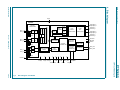
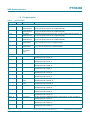
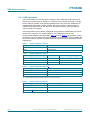
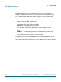
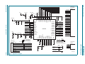
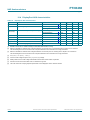
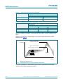
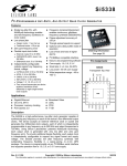
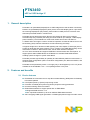
PTN3460
NXP Semiconductors
eDP to LVDS bridge IC
7. Pinning information
43 LVSDO_P
44 LVSDO_N
45 VDD(1V8)
46 LVSCKO_P
47 LVSCKO_N
48 LVSCO_P
49 LVSCO_N
50 VDD(3V3)
51 LVSBO_P
52 LVSBO_N
53 LVSAO_P
54 LVSAO_N
terminal 1
index area
55 n.c.
56 EPS_N
7.1 Pinning
AUX_N
1
42 LVSAE_N
AUX_P
2
41 LVSAE_P
GND
3
40 LVSBE_N
DP0_P
4
39 LVSBE_P
DP0_N
5
38 VDD(3V3)
VDD(1V8)
6
37 LVSCE_N
DP1_P
7
DP1_N
8
35 LVSCKE_N
RST_N
9
34 LVSCKE_P
36 LVSCE_P
PTN3460BS
PD_N 10
33 PVCCEN
HPDRX 11
32 LVSDE_N
DEV_CFG 12
31 LVSDE_P
(1)
PWMO 28
CFG4 27
BKLTEN 26
MS_SCL 25
MS_SDA 24
CFG3 23
CFG2 22
CFG1 21
TESTMODE 20
VDD(1V8) 19
GNDREG 18
GNDREG 17
29 DDC_SCL
n.c. 16
30 DDC_SDA
VDD(3V3) 14
n.c. 15
VDD(3V3) 13
002aaf833
Transparent top view
(1) Center pad is connected to PCB ground plane for electrical grounding and thermal relief.
Fig 3.
Pin configuration for HVQFN56
Refer to Section 13 “Package outline” for package and pin dimensions.
PTN3460
Product data sheet
All information provided in this document is subject to legal disclaimers.
Rev. 4 — 12 March 2014
© NXP Semiconductors N.V. 2014. All rights reserved.
5 of 32