1
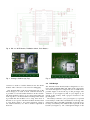
Fig. 5. GL865 GSM Module, SIM-Card Holder and SiP32411 Load Switch
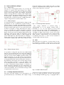
header (JP3 , see Figure 4) which makes it possible to
measure the current used by the GPS-receiver. For normal use this header should be shorted electrically. The
receiver is connected to a backup-voltage which keeps
the internal RTC running this decreases the Time To First
Fix (TTFF) after a power-on event. A diode is used to
power the backup-circuit of the GPS-receiver because it
is also possible to use an ultracap in combination with
the A1035-H in applications where no battery is used.
This diode protects the charge-circuit inside the GPSModule. For communication with the Wi-Fi-module, two
UART lines are used (Tx and Rx ). The header JP4 (see
Figure 4) can be used to connect a logic analyzer during
debugging. The GPS-module is switched off when it is
not used. This is done by the Wi-Fi module, it emits
a short positive pulse on the line connected to pin 17
from the GPS module. Sending another pulse switches
the module to the on state.
2.4
GSM/GPRS
In Figure 5 the circuit of the GL865 GSM-Module is
shown. It also contains a SIM-Card Holder and a Load
Switch (SiP32411).
There are two types of the GL865 module available
on the market, the GL865-DUAL and GL865-QUAD. The
GL865-DUAL can be used in countries where operators
use the 900 MHz and 1800 MHz frequency bands. These
are the frequencies used in Europe. The GL865-QUAD
can also be used with the 850 MHz and 1900 MHz
frequencies but uses a little more power.
If the GL865 is in idle-mode it is possible to disconnect
it’s power-supply on pin 38. This is not necessary but
it will lower the battery-consumption with a current of
approx. 630µA [3]. The load switch makes it possible
to disconnect and re-connect the power to the GSMmodule by switching a simple enable-signal [4]. This
enable-signal is controlled by the Wi-Fi-module.
Like the GPS-receiver, the GSM-module also needs
a backup voltage. This voltage makes it possible to
get a faster connection with the GSM network after a
power-on event. JP6 (see Figure 5) is a test-header to
measure the current used by the GSM-module. A logic
analyser can be placed on header JP5 (see Figure 5) for
easy debugging. JP5 is placed on the two UART lines
which are used to create a connection between the GSMmodule and Wi-Fi-module. The GSM-module accepts
voltages as high as 2.8 Volt on the receiving UART pin.
A voltage divider (R6 and R7 in Figure 5) is used to
reduce the higher voltage (3.3 Volt) that is placed by the
Wi-Fi-module on the Tx line.
2.5
Wi-Fi
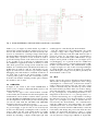
Figure 6 shows the circuit of the RN-171 Wi-Fi-module.
This module is designed for applications where energy
consumption is a critical issue. A tilt/motion switch is
used to detect movement of the tag. The state of this
switch is checked using the current loop sensor inside
the Wi-Fi-module [5]. Three LEDs are used for debugging and signalizing, a logic analyzer can be connected
to JP8 (see Figure 6). A standard push-button is also
integrated on the board. R13 is a pull-up resistor, C17
is used for de-bouncing, R14 is responsible for recharge
the debounce-capacitor once the push-button is opened
again. JP7 (see Figure 6) is used to measure the current used by the Wi-Fi-module. For communication
with the GSM-receiver and GPS-module, two UART
communication lines are used. Other lines are used to
check the power-state from the GSM-module, control the
load switch, and change the power-state from the GPSmodule. For measuring the battery voltage, a voltage
divider (R8 and R9 ) is used because the sensor-inputs
can only measure voltages up to 400 mV. A 16-pins ISP-