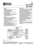
1
ADSP-218x DSP Instruction Set Reference First Edition, February 2001 Part Number 82-002000-01 Analog Devices, Inc. Digital Signal Processor Division One Technology Way Norwood, Mass. 02062-9106 a Copyright Information ©1996–2001 Analog Devices, Inc., ALL RIGHTS RESERVED. This document may not be reproduced in any form without prior, express written consent from Analog Devices, Inc. Printed in the USA. Disclaimer Analog Devices, Inc. reserves the right to change this product without prior notice. Information furnished by Analog Devices is believed to be accurate and reliable. However, no responsibility is assumed by Analog Devices for its use; nor for any infringement of patents or other rights of third parties which may result from its use. No license is granted by implication or otherwise under the patent rights of Analog Devices, Inc. Trademark and Service Mark Notice The Analog Devices logo, VisualDSP, the VisualDSP logo, EZ-ICE, and EZ-LAB are registered trademarks; and, the White Mountain logo, Apex-ICE, Mountain-ICE, Mountain-ICE/WS, Summit-ICE, Trek-ICE, Vista-ICE, and The DSP Collaborative are trademarks of Analog Devices, Inc. Microsoft and Windows are registered trademarks and Windows NT is a trademark of Microsoft Corporation. Adobe and Acrobat are registered trademarks of Adobe Corporation. All other brand and product names are trademarks or service marks of their respective owners. CONTENTS CONTENTS INTRODUCTION Purpose ......................................................................................... 1-1 Audience ...................................................................................... 1-1 Contents Overview ....................................................................... 1-2 Development Tools ....................................................................... 1-3 For More Information About Analog Products ............................... 1-6 For Technical or Customer Support ............................................. 1-7 What’s New in This Manual .......................................................... 1-7 Related Documents ....................................................................... 1-8 Conventions ................................................................................. 1-9 PROGRAMMING MODEL Overview ...................................................................................... 2-1 Data Address Generators .......................................................... 2-4 Program Sequencer .................................................................. 2-5 Computational Units ............................................................... 2-7 Bus Exchange .......................................................................... 2-8 ADSP-218x Instruction Set Reference i CONTENTS Timer ..................................................................................... 2-8 Serial Ports .............................................................................. 2-8 Memory Interface & SPORT Enables .................................... 2-10 Program Example ....................................................................... 2-12 Example Program: Setup Routine Discussion ......................... 2-14 Example Program: Interrupt Routine Discussion .................... 2-15 Hardware Overlays and Software Issues ....................................... 2-17 Libraries and Overlays ........................................................... 2-18 Interrupts and Overlays ......................................................... 2-18 Loop Hardware and Overlays ................................................ 2-20 SOFTWARE EXAMPLES Overview ...................................................................................... 3-1 System Development Process ....................................................... 3-3 Single-Precision Fir Transversal Filter ............................................ 3-6 Cascaded Biquad IIR Filter ........................................................... 3-8 Sine Approximation .................................................................... 3-10 Single-Precision Matrix Multiply ................................................. 3-12 Radix-2 Decimation-in-Time FFT .............................................. 3-14 Main Module ........................................................................ 3-14 DIT FFT Subroutine ............................................................ 3-16 Bit-Reverse Subroutine .......................................................... 3-21 Block Floating-Point Scaling Subroutine ................................ 3-22 ii ADSP-218x Instruction Set Reference CONTENTS INSTRUCTION SET Quick List Of Instructions ............................................................ 4-1 ALU Instructions ..................................................................... 4-1 MAC Instructions ................................................................... 4-2 Shifter Instructions .................................................................. 4-2 Move Instructions ................................................................... 4-3 Program Flow Instructions ....................................................... 4-3 MISC Instructions .................................................................. 4-4 Multifunction Instructions ...................................................... 4-4 Overview ...................................................................................... 4-5 Multifunction Instructions ............................................................ 4-7 ALU/MAC with Data and Program Memory Read ................... 4-7 Data and Program Memory Read ............................................. 4-8 Computation with Memory Read ............................................ 4-9 Computation With Memory Write .......................................... 4-9 Computation with Data Register Move .................................. 4-10 ALU, MAC & Shifter Instructions ............................................... 4-14 ALU Group ........................................................................... 4-14 MAC Group .......................................................................... 4-17 Shifter Group ........................................................................ 4-19 MOVE: Read and Write Instructions ........................................... 4-21 Program Flow Control ................................................................ 4-23 Miscellaneous Instructions .......................................................... 4-26 Extra Cycle Conditions ............................................................... 4-28 ADSP-218x Instruction Set Reference iii CONTENTS Multiple Off-Chip Memory Accesses ..................................... 4-28 Wait States ............................................................................ 4-28 SPORT Autobuffering and DMA .......................................... 4-29 Instruction Set Syntax ................................................................. 4-29 Punctuation and Multifunction Instructions .......................... 4-29 Syntax Notation Example ...................................................... 4-30 Status Register Notation ........................................................ 4-31 ALU Instructions ........................................................................ 4-32 Add/Add with Carry ............................................................. 4-32 Subtract X-Y/Subtract X-Y with Borrow ................................ 4-35 Subtract Y-X/Subtract Y-X with Borrow ................................. 4-39 Bitwise Logic: AND, OR, XOR ............................................. 4-42 Bit Manipulation: TSTBIT, SETBIT, CLRBIT, TGLBIT ....... 4-45 Clear: PASS .......................................................................... 4-48 Negate .................................................................................. 4-53 NOT .................................................................................... 4-55 Absolute Value: ABS ............................................................. 4-57 Increment ............................................................................. 4-60 Decrement ............................................................................ 4-62 Divide Primitives: DIVS and DIVQ ...................................... 4-64 Generate ALU Status Only: NONE ....................................... 4-72 MAC Instructions ...................................................................... 4-74 Multiply ............................................................................... 4-74 Multiply with Cumulative Add .............................................. 4-78 iv ADSP-218x Instruction Set Reference CONTENTS Multiply with Cumulative Subtract ........................................ 4-82 Squaring ............................................................................... 4-86 MAC Clear ........................................................................... 4-90 MAC Transfer MR ................................................................ 4-92 Conditional MR Saturation ................................................... 4-95 Shifter Instructions ..................................................................... 4-97 Arithmetic Shift .................................................................... 4-97 Logical Shift ........................................................................ 4-100 Normalize ........................................................................... 4-103 Derive Exponent ................................................................. 4-106 Block Exponent Adjust ........................................................ 4-110 Arithmetic Shift Immediate ................................................. 4-112 Logical Shift Immediate ....................................................... 4-114 Move Instructions ..................................................................... 4-116 Register Move ..................................................................... 4-116 Load Register Immediate ..................................................... 4-118 Data Memory Read (Direct Address) .................................... 4-121 Data Memory Read (Indirect Address) ................................. 4-123 Program Memory Read (Indirect Address) ............................ 4-125 Data Memory Write (Direct Address) ................................... 4-127 Data Memory Write (Indirect Address) ................................ 4-129 Program Memory Write (Indirect Address) ........................... 4-132 IO Space Read/Write ........................................................... 4-134 Program Flow Instructions ........................................................ 4-136 ADSP-218x Instruction Set Reference v CONTENTS JUMP ................................................................................. 4-136 CALL ................................................................................. 4-139 JUMP or CALL on Flag In Pin ............................................ 4-141 Modify Flag Out Pin ........................................................... 4-143 RTS (Return from Subroutine) ............................................ 4-145 RTI (Return from Interrupt) ............................................... 4-147 Do Until ............................................................................. 4-149 Idle ..................................................................................... 4-153 MISC Instructions .................................................................... 4-155 Stack Control ...................................................................... 4-155 TOPPCSTACK .................................................................. 4-158 Mode Control ..................................................................... 4-161 Interrupt Enable and Disable ............................................... 4-164 Program Memory Overlay Register Update .......................... 4-165 Data Memory Overlay Register Update ................................ 4-168 Modify Address Register ...................................................... 4-171 No Operation ..................................................................... 4-173 Multifunction Instructions ........................................................ 4-174 Computation with Memory Read ........................................ 4-174 Computation with Register to Register Move ....................... 4-180 Computation with Memory Write ....................................... 4-185 Data and Program Memory Read ......................................... 4-190 ALU/MAC with Data and Program Memory Read ............... 4-192 vi ADSP-218x Instruction Set Reference CONTENTS INSTRUCTION CODING Overview ..................................................................................... A-1 Opcode Definitions ..................................................................... A-2 Opcode Mnemonics ................................................................... A-10 INDEX ADSP-218x Instruction Set Reference vii CONTENTS viii ADSP-218x Instruction Set Reference 1 INTRODUCTION Figure 1-0. Table 1-0. Listing 1-0. Purpose The ADSP-218x DSP Instruction Set Reference provides assembly syntax information for the ADSP-218x Digital Signal Processor (DSP). The syntax descriptions for instructions that execute within the DSP’s processor core include processing elements, program sequencer, and data address generators. For architecture and design information on the DSP, see the ADSP-218x DSP Hardware Reference. Audience DSP system designers and programmers who are familiar with signal processing concepts are the primary audience for this manual. This manual assumes that the audience has a working knowledge of microcomputer technology and DSP-related mathematics. DSP system designers and programmers who are unfamiliar with signal processing can use this manual, but should supplement this manual with other texts, describing DSP techniques. All readers, particularly programmers, should refer to the DSP’s development tools documentation for software development information. For additional suggested reading, see the section “For More Information About Analog Products” on page 1-6. ADSP-218x DSP Instruction Set Reference 1-1 Contents Overview Contents Overview The Instruction Set Reference is a four chapter book that describes the instructions syntax for the ADSP-218x DSP. Chapter one provides introductory information including contacts at Analog Devices, an overview of the development tools, related documentation and conventions. Chapter two describes the computational units of the ADSP-218x DSP and provides a programming example with discussion. Chapter three describes the process to create executable programs for the ADSP-218x DSP. It provides several software examples that can be used to create programs. Chapter four presents information organized by the type of instruction. Instruction types relate to the machine language opcode for the instruction. On this DSP, the opcodes categorize the instructions by the portions of the DSP architecture that execute the instructions. Each reference page for an instruction shows the syntax of the instruction, describes its function, gives one or two assembly-language examples, and identifies fields of its opcode. The instructions are also referred to by type, ranging from 1 to 31. These types correspond to the opcodes that ADSP-218x DSPs recognize, but are for reference only and have no bearing on programming. Some instructions have more than one syntactical form; for example, instruction “Multiply” on page 4-75 has many distinct forms. Many instructions can be conditional. These instructions are prefaced by for example: IF cond; IF EQ MR = MX0 * MY0 (SS); In a conditional instruction, the execution of the entire instruction is based on the condition. 1-2 ADSP-218x DSP Instruction Set Reference Introduction The following instructions groups are available for ADSP-218x DSP: • “Quick List Of Instructions” on page 4-1—This section provides a a quick reference to all instructions. • “ALU Instructions” on page 4-32—These instruction specify operations that occur in the DSP’s ALU. • “MAC Instructions” on page 4-75—These instructions specify operations that occur in the DSP’s Multiply–Accumulator. • “Shifter Instructions” on page 4-97—These instructions specify operations that occur in the DSP’s Shifter. • “Multifunction Instructions” on page 4-174—These instructions specify parallel, single-cycle operations. • “Move Instructions” on page 4-116—These instructions specify memory and register access operations. • “Program Flow Instructions” on page 4-136—These instructions specify program sequencer operations. Appendix A lists the instruction encoding fields by type number and defines opcode mnemonics as listed alphabetically. Development Tools The ADSP-218x is supported by VisualDSP++®, an easy-to-use programming environment, comprised of an Integrated Development Environment (IDE) and Debugger. VisualDSP lets you manage projects from start to finish from within a single, integrated interface. Because the project development and debug environments are integrated, you can move easily between editing, building, and debugging activities. ADSP-218x DSP Instruction Set Reference 1-3 Development Tools Flexible Project Management. The IDE provides flexible project management for the development of DSP applications. The IDE includes access to all the activities necessary to create and debug DSP projects. You can create or modify source files or view listing or map files with the IDE Editor. This powerful Editor is part of the IDE and includes multiple language syntax highlighting, OLE drag and drop, bookmarks, and standard editing operations such as undo/redo, find/replace, copy/paste/cut, and goto. Also, the IDE includes access to the C Compiler, C Runtime Library, Assembler, Linker, Loader, Simulator, and Splitter. You specify options for these tools through Property Page dialogs. Property Page dialogs are easy to use, and make configuring, changing, and managing your projects simple. These options control how the tools process inputs and generate outputs, and have a one-to-one correspondence to the tools’ command line switches. You can define these options once, or modify them to meet changing development needs. You can also access the tools from the operating system command line if you choose. Greatly Reduced Debugging Time. The Debugger has an easy-to-use, common interface for all processor simulators and emulators available through Analog Devices and third parties or custom developments. The Debugger has many features that greatly reduce debugging time. You can view C source interspersed with the resulting Assembly code. You can profile execution of a range of instructions in a program; set simulated watch points on hardware and software registers, program and data memory; and trace instruction execution and memory accesses. These features enable you to correct coding errors, identify bottlenecks, and examine DSP performance. You can use the custom register option to select any combination of registers to view in a single window. The Debugger can also generate inputs, outputs, and interrupts so you can simulate real world application conditions. Software Development Tools. The Software Development Tools, which support the ADSP-218x Family, allow you to develop applications that 1-4 ADSP-218x DSP Instruction Set Reference Introduction take full advantage of the DSP architecture, including shared memory and memory overlays. Software Development tools include C Compiler, C Runtime Library, DSP and Math Libraries, Assembler, Linker, Loader, Simulator, and Splitter. C Compiler & Assembler. The C Compiler generates efficient code that is optimized for both code density and execution time. The C Compiler allows you to include Assembly language statements inline. Because of this, you can program in C and still use Assembly for time-critical loops. You can also use pretested Math, DSP, and C Runtime Library routines to help shorten your time to market. The ADSP-218x Family Assembly language is based on an algebraic syntax that is easy to learn, program, and debug. The add instruction, for example, is written in the same manner as the actual equation using registers for variables (for example, AR = AX0 + AY0;). Linker & Loader. The Linker provides flexible system definition through Linker Description Files (.LDF). In a single LDF, you can define different types of executables for a single or multiprocessor system. The Linker resolves symbols over multiple executables, maximizes memory use, and easily shares common code among multiple processors. The Loader supports creation of a 16-bit host port and 8-bit PROM boot images. Along with the Linker, the Loader allows a variety of system configurations with smaller code and faster boot time. Simulator. The Simulator is a cycle-accurate, instruction-level simulator that allows you to simulate your application in real time. Emulator. The EZ-ICE serial emulator system provides state-of-the-art emulation for the ADSP-218x family of DSPs using a controlled environment for observing, debugging, and testing activities in a target system. The key features of the ADSP-218x EZ-ICE include a shielded enclosure with the reset switch, a high speed RS-232 serial port interface, and support for 2.5, 3.3 and 5.0V DSPs. The EZ-ICE connects directly to the target processor via the emulation interface port. It’s ease of use, full ADSP-218x DSP Instruction Set Reference 1-5 For More Information About Analog Products speed emulation, and shield board will ensure that your design process runs smoothly. 3rd-Party Extensible. The VisualDSP environment enables third-party companies to add value using Analog Devices’ published set of Application Programming Interfaces (API). Third party products including runtime operating systems, emulators, high-level language compilers, multiprocessor hardware can interface seamlessly with VisualDSP thereby simplifying the tools integration task. VisualDSP follows the COM API format. Two API tools, Target Wizard and API Tester, are also available for use with the API set. These tools help speed the time-to-market for vendor products. Target Wizard builds the programming shell based on API features the vendor requires. The API tester exercises the individual features independently of VisualDSP. Third parties can use a subset of these APIs that meets their application needs. The interfaces are fully supported and backward compatible. Further details and ordering information are available in the VisualDSP Development Tools data sheet. This data sheet can be requested from any Analog Devices sales office or distributor. For More Information About Analog Products Analog Devices can be found on the internet at http://www.analog.com. Our Web pages provide information about the company and products, including access to technical information and documentation, product overviews, and product announcements. You may obtain additional information about Analog Devices and its products in any of the following ways: • Visit our World Wide Web site at www.analog.com • FAX questions or requests for information to 1(781)461-3010. 1-6 ADSP-218x DSP Instruction Set Reference Introduction • Access the Computer Products Division File Transfer Protocol (FTP) site at ftp ftp.analog.com or ftp 137.71.23.21 or ftp://ftp.analog.com. For Technical or Customer Support You can reach our Customer Support group in the following ways: • E-mail questions to [email protected], [email protected] or [email protected] (European customer support) • Telex questions to 924491, TWX:710/394-6577 • Cable questions to ANALOG NORWOODMASS • Contact your local ADI sales office or an authorized ADI distributor • Send questions by mail to: Analog Devices, Inc. DSP Division One Technology Way P.O. Box 9106 Norwood, MA 02062-9106 USA What’s New in This Manual This is the preliminary edition of the ADSP-218x DSP Instruction Set Reference. Summaries of changes between editions will start with the next edition. ADSP-218x DSP Instruction Set Reference 1-7 Related Documents Related Documents For more information about Analog Devices DSPs and development products, see the following documents: • ADSP-218x DSP Hardware Reference • Getting Started Guide for VisualDSP & ADSP-218x Family DSPs • VisualDSP User's Guide for ADSP-218x Family DSPs • C Compiler & Library Manual for ADSP-218x Family DSPs • Assembler Manual for ADSP-218x Family DSPs • Linker & Utilities Manual for ADSP-218x Family DSPs All the manuals are included in the software distribution CD-ROM. To access these manuals, use the Help Topics command in the VisualDSP environment’s Help menu and select the Online Manuals book. From this Help topic, you can open any of the manuals, which are in Adobe Acrobat PDF format. 1-8 ADSP-218x DSP Instruction Set Reference Introduction Conventions Throughout this manual you will find tables summarizing the syntax of the instruction groups. Table 1-1 identifies the notation conventions that apply to all chapters. Note that additional conventions, which apply only to specific chapters, may appear throughout this manual. Table 1-1. Instruction set notation Notation Meaning UPPERCASE Explicit syntax—assembler keyword. The assembler is caseinsensitive. ; A semicolon terminates an instruction line. , A comma separates multiple, parallel instructions in the same instruction line. // single line comment /* multi line comment */ // or /* */ indicate comments or remarks that explain program code, but that the assembler ignores. For more details, see the Assembler Manual for ADSP-218x Family DSPs. operands Some instruction operands are shown in lowercase letters. These operands may take different values in assembly code. For example, the operand yop may be one of several registers: AY0, AY1, or AF. <exp> Denotes exponent (shift value) in Shift Immediate instructions; must be an 8-bit signed integer constant. <data> Denotes an immediate data value. <addr> Denotes an immediate address value to be encoded in the instruction. The <addr> may be either an immediate value (a constant) or a program label. <reg> Refers to any accessible register; see the table “Processor Registers: reg and dreg” on page 4-22. ADSP-218x DSP Instruction Set Reference 1-9 Conventions Table 1-1. Instruction set notation (Cont’d) Notation Meaning [brackets] Refers to optional instruction extensions <dreg> Refers to any data register; see the table “Processor Registers: reg and dreg” on page 4-22. 0x Denotes number in hexadecimal format (0xFFFF). h# Denotes number in hexadecimal format (h#FFFF). b# Denotes number in binary format (b#0001000100010001). Immediate values such as <exp>, <data>, or <addr> may be a constant in decimal, hexadecimal, octal or binary format. The default format is decimal. 1-10 ADSP-218x DSP Instruction Set Reference 2 PROGRAMMING MODEL Figure 2-0. Table 2-0. Listing 2-0. Overview From a programming standpoint, the ADSP-218x processors consist of three computational units (ALU, MAC and Shifter), two data address generators, and a program sequencer, plus on-chip peripherals and memory that vary with each processor. Almost all operations using these architectural components require one or more registers to store data, to keep track of values such as pointers, or to specify operating modes. Internal registers hold data, addresses, control information or status information. For example, AX0 stores an ALU operand (data); I4 stores a DAG2 pointer (address); ASTAT contains status flags from arithmetic operations; fields in the wait state register control the number of wait states for different zones of external memory. There are two types of accesses for registers. The first type of access is made to dedicated registers such as MX0 and IMASK. These registers can be read and written explicitly in assembly language. For example: MX0=1234; IMASK=0xF; The second type of access is made to memory-mapped registers such as the system control register, wait state control register, timer registers and SPORT registers. These registers are accessed by reading and writing the corresponding data memory locations. For example, the following code ADSP-218x Instruction Set Reference 2-1 Overview clears the Wait State Control Register, which is mapped to data memory location 0x3FFE: AX0=0; DM(0x3FFE)=AX0; In this example, AX0 is used to hold the constant 0 because there is no instruction to write an immediate data value to memory using an immediate address. 2-2 ADSP-218x Instruction Set Reference Programming Model The ADSP-218x registers are shown in Figure 2-1. The registers are grouped by function: data address generators (DAGs), program sequencer, computational units (ALU, MAC, and shifter), bus exchange (PX), memory interface, timer, SPORTs, host interface, and DMA interface. Processor Core DATA ADDRESS GENERATORS DAG1 (DM addressing only) DAG2 (DM and PM addressing) Bit-reverse capability Indirect branch capability TIMER MEMORY INTERFACE 0x3FFD TPERIOD I0 L0 M0 I4 L4 M4 I1 L1 M1 I5 L5 M5 I2 L2 M2 I6 L6 M6 I3 L3 14 M3 I7 14 L7 M7 14 14 14 14 0x3FFC TCOUNT 0x3FFB TSCALE System Control Register Wait States 4 4 DMOVLAY PMOVLAY 0x3FFF 0x3FFE SPORT 0 PROGRAM SEQUENCER 18 5 LOOP STACK 4 X 18 RX0 14 ICNTL 16 IFC* 14 CNT R COUNT STACK 4 X 14 0x3FFA SSTAT OWRCNTR 10 7 IMASK* 8 MSTAT* ASTAT RX 31-16 0x3FF9 RX 15-0 0x3FF8 TX 31-16 0x3FF7 TX 15-0 SPORT0 Control STATUS STACK* * Status Stack Depth = 12 memory locations, Width = 25 bits ALU TX0 Multichannel enables PC STACK 16 X 14 8 0x3FF6 Control 0x3FF5 SCLKDIV 0x3FF4 0x3FF3 Autobuffer IDMA PORT BDMA PORT PROGRAMMABLE FLAGS RFSDIV MAC IDMA Registers 0x3FE0 IDMA Control Register BDMA Registers 0x3FE4 BWCOUNT 0x3FE3 BDMA Control AX0 AX1 AY0 AY1 MX0 MX1 8 AR AF 16 MY0 MY1 MR2 MR1 MR0 MF RX1 TX1 SPORT1 Control SHIFTER 16 8 SI BUS EXCHANGE 5 SE 8 SB Programmable Flag Registers 0x3FE2 BEAD 0x3FE6 PFTYPE 0x3FE1 BIAD 0x3FE5 PFDATA SPORT 1 16 PX 0x3FF2 Control 0x3FF1 SCLKDIV RFSDIV 0x3FF0 0x3FEF Autobuffer SR1 SR0 Figure 2-1. ADSP-218x DSP Registers ADSP-218x Instruction Set Reference 2-3 Overview Data Address Generators DAG1 and DAG2 each have twelve 14-bit registers: four index (I) registers for storing pointers, four modify (M) registers for updating pointers and four length (L) registers for implementing circular buffers. DAG1 addresses data memory only and has the capability of bit-reversing its outputs. DAG2 addresses both program and data memory and can provide addresses for indirect branching (jumps and calls) as well as for accessing data. The following example is an indirect data memory read from the location pointed to by I0. Once the read is complete, I0 is updated by M0. AX0=DM(I0,M0); The following example is an indirect program memory data write to the address pointed to by I4 with a post modify by M5: PM(I4,M5)=MR1; The following example is an example of an indirect jump: JUMP (I4); Always Initialize L Registers The ADSP-218x processors allow two addressing modes for data memory accesses: direct and register indirect. Indirect addressing is accomplished by loading an address into an I (index) register and specifying one of the available M (modify) registers. The L registers are provided to facilitate wraparound addressing of circular data buffers. A circular buffer is only implemented when an L register is set to a non-zero value. ! For linear (i.e. non-circular) indirect addressing, the register corresponding to the I register used must be set to zero. Do not assume that the L registers are automatically initialized or may be ignored; the 2-4 ADSP-218x Instruction Set Reference L Programming Model I, M, and L registers contain random values following processor reset. Your program must initialize the L registers corresponding to any I registers it uses. Program Sequencer Registers associated with the program sequencer control subroutines, loops, and interrupts. They also indicate status and select modes of operation. Interrupts The ICNTL register controls interrupt nesting and external interrupt sensitivity. The IFC register which is 16 bits wide lets you force and clear interrupts in software. The IMASK register which is 10 bits wide masks (disables) individual interrupts. ADSP-218x processors support 12 interrupts, two of which (reset, powerdown) are non-maskable. The ADSP-2181 supports a global interrupt enable instruction (ENA INTS) and interrupt disable instruction (DIS INTS). Executing the disable interrupt instruction causes all interrupts to be masked without changing the contents of the IMASK register. Disabling interrupts does not affect serial port autobuffering, which will operate normally whether or not interrupts are enabled. The disable interrupt instruction masks all user interrupts including the powerdown interrupt. The interrupt enable instruction allows all unmasked interrupts to be serviced again. Loop Counts The CNTR register stores the count value for the currently executing loop. The count stack allows the nesting of count-based loops to four levels. A write to CNTR pushes the current value onto the count stack before writing ADSP-218x Instruction Set Reference 2-5 Overview the new value. The following example pushes the current value of CNTR on the count stack and then loads CNTR with 10. CNTR=10; is a special syntax with which you can overwrite the count value for the current loop without pushing CNTR on the count stack. OWRCNTR " cannot be read (i.e. used as a source register), and must not be written in the last instruction of a DO UNTIL loop. OWRCNTR Status And Mode Bits The stack status (SSTAT) register contains full and empty flags for stacks. The arithmetic status (ASTAT) register contains status flags for the computational units. The mode status (MSTAT) register contains control bits for various options. MSTAT contains 4 bits that control alternate register selection for the computational units, bit-reverse mode for DAG1, and overflow latch and saturation modes for the ALU. MSTAT also has 3 bits to control the MAC result placement, timer enable, and Go mode enable. Use the Mode Control instruction (ENA or disable processor modes. DIS) to conveniently enable or Stacks The program sequencer contains four stacks that allow loop, subroutine and interrupt nesting. The PC stack is 14 bits wide and 16 locations deep. It stores return addresses for subroutines and interrupt service routines, and top-of-loop addresses for loops. PC stack handling is automatic for subroutine calls and interrupt handling. In addition, the PC stack can be manually pushed or popped using the PC Stack Control instructions TOPPCSTACK=reg and reg=TOPPCSTACK. 2-6 ADSP-218x Instruction Set Reference Programming Model The loop stack is 18 bits wide, 14 bits for the end-of-loop address and 4 bits for the termination condition code. The loop stack is four locations deep. It is automatically pushed during the execution of a DO UNTIL instruction. It is popped automatically during a loop exit if the loop was nested. The loop stack may be manually popped with the POP LOOP instruction. The status stack, which is automatically pushed when the processor services an interrupt, accommodates the interrupt mask (IMASK), mode status (MSTAT) and arithmetic status (ASTAT) registers. The depth and width of the status stack varies with each processor, since each of the processors has a different numbers of interrupts. The status stack is automatically popped when the return from interrupt (RTI) instruction is executed. The status stack can be pushed and popped manually with the PUSH STS and POP STS instructions. The count stack is 14 bits wide and holds counter (CNTR) values for nested counter-based loops. This stack is pushed automatically with the current CNTR value when there is a write to CNTR. The counter stack may be manually popped with the POP CNTR instruction. Computational Units The registers in the computational units store data. The ALU and MAC require two inputs for most operations. The AX0, AX1, MX0, and MX1 registers store X inputs, and the AY0, AY1, MY0, and MY1 registers store Y inputs. The AR and AF registers store ALU results; AF can be fed back to the ALU Y input, whereas AR can provide the X input of any computational unit. Likewise, the MR0, MR1, MR2, and MF register store MAC results and can be fed back for other computations. The 16-bit MR0 and MR1 registers together with the 8-bit MR2 register can store a 40-bit multiply/accumulate result. The shifter can receive input from the ALU or MAC, from its own result registers, or from a dedicated shifter input (SI) register. It can store a 32-bit result in the SR0 and SR1 registers. The SB register stores the block ADSP-218x Instruction Set Reference 2-7 Overview exponent for block floating-point operations. The SE register holds the shift value for normalize and denormalize operations. Registers in the computational units have secondary registers, shown in Figure 2-1 as second set of registers behind the first set. Secondary registers are useful for single-cycle context switches. The selection of these secondary registers is controlled by a bit in the MSTAT register; the bit is set and cleared by these instructions: ENA SEC_REG; /*select secondary registers*/ DIS SEC_REG; /*select primary registers*/ Bus Exchange The PX register is an 8-bit register that allows data transfers between the 16-bit DMD bus and the 24-bit PMD bus. In a transfer between program memory and a 16-bit register, PX provides or receives the lower eight bits implicitly. Timer The TPERIOD, TCOUNT, and TSCALE hold the timer period, count, and scale factor values, respectively. These registers are memory-mapped at locations 0x3FFD, 0x3FFC, and 0x3FFB respectively. Serial Ports SPORT0 and SPORT1 each have receive ( RX), transmit (TX) and control registers. The control registers are memory-mapped registers at locations 0x3FEF through 0x3FFA in data memory. SPORT0 also has registers for controlling its multichannel functions. Each SPORT control register contains bits that control frame synchronization, companding, word length and, in SPORT0, multichannel options. The SCLKDIV register for each SPORT determines the frequency of the internally generated serial clock, 2-8 ADSP-218x Instruction Set Reference Programming Model and the RFSDIV register determines the frequency of the internally generated receive frame sync signal for each SPORT. The autobuffer registers control autobuffering in each SPORT. Programming a SPORT consists of writing to its control register and, depending on the modes selected, writing to its SCLKDIV and/or RFSDIV registers as well. The following example code programs SPORT0 for 8-bit µ-law companding with normal framing and an internally generated serial clock. RFSDIV is set to 255 for 256 SCLK cycles between RFS assertions. SCLKDIV is set to 2, resulting in an SCLK frequency that is 1/6 of the CLKIN frequency. SI=0xB27; DM(0X3FF6)=SI; /*SPORT0 control register*/ SI=2; DM(0x3FF5)=SI; /*SCLKDIV = 2*/ SI=255; DM(0x3FF4)=SI; /*RFSDIV = 255*/ ADSP-218x Instruction Set Reference 2-9 Overview Memory Interface & SPORT Enables The system control register, memory-mapped at DM(0x3fff), contains SPORT0 and SPORT1 enable bits (bits 12 and 11 respectively) as well as the SPORT1 configuration selection bit (bit 10). On all ADSP-218x processors, the system control register also contains fields for external program memory wait states. For the following processors, the system control register contains the disable BMS bit, which allows the external signal BMS to be disabled during byte memory accesses. This feature can be used, for example, to allow the DSP to boot from an EPROM and then access a flash, or other byte-wide device, at runtime via the CMS signal. ADSP-2184 ADSP-2184L ADSP-2185M ADSP-2184N ADSP-2186 ADSP-2185L ADSP-2186M ADSP-2185N ADSP-2186L ADSP-2188M ADSP-2186N ADSP-2187L ADSP-2189 M ADSP-2187N ADSP-2188N ADSP-2189 N The wait state control register, memory-mapped at DM(0x3ffe), contains fields that specify the number of wait states for external data memory, and four banks of external I/O memory space. On the following processors, bit 15 of the register, the wait state mode select bit, determines whether the assigned wait state value operates in a “1x” or “2x+1” mode: 2-10 ADSP-2185M ADSP-2185N ADSP-2186M ADSP-2186N ADSP-2188M ADSP-2187N ADSP-218x Instruction Set Reference Programming Model ADSP-2189M ADSP-2188N ADSP-2189N Other memory-mapped registers control the IDMA port and byte memory DMA (BDMA) port for booting and runtime operations. These registers can be used in many ways that includes selecting the byte memory page, operating in data packing mode, or forcing the boot from software. ADSP-218x Instruction Set Reference 2-11 Program Example Program Example Listing 2-1 presents an example of an FIR filter program written for the ADSP-2181 followed by a discussion of each part of the program. The program can also be executed on any other ADSP-218x processor, with minor modifications. This FIR filter program demonstrates much of the conceptual power of the ADSP-218x family architecture and instruction set. Listing 2-1. Include File, Constants Initialization /*ADSP-2181 FIR Filter Routine -serial port 0 used for I/O -internally generated serial clock -40.000 MHz processor clock rate is divided to generate a 1.5385 MHz serial clock -serial clock divided to 8 kHz frame sampling rate*/ A #include <def2181.h> #define taps 15 #define taps_less_one 14 B .section/dm .var/circ dm_data; data_buffer[taps]; .section/pm .var/circ/init24 pm_data; coefficient[taps] = "coeff.dat"; C 2-12 /* dm data buffer */ .section/pm Interrupts; start: jump main; rti; rti; rti; /* 0x0000: ~Reset vector rti; rti; rti; rti; /* 0x0004: ~IRQ2 rti; rti; rti; rti; ‘ /* 0x0008: ~IRQL1 rti; rti; rti; rti; /* 0x000c: ~IRQL0 rti; rti; rti; rti; /* 0x0010: SPORT0 Transmit jump fir_start; rti; rti; rti; /* 0x0014: SPORT0 Receive rti; rti; rti; rti; /* 0x0018: ~IRQE rti; rti; rti; rti; /* 0x001c: BDMA rti; rti; rti; rti; /* 0x0020: SPORT1 Transmit or ~IRQ1 rti; rti; rti; rti; /* 0x0024: SPORT1 Receive or ~IRQ0 ADSP-218x Instruction Set Reference */ */ */ */ */ */ */ */ */ */ Programming Model D rti; rti; rti; rti; /* 0x0028: Timer rti; rti; rti; rti; /* 0x002c: Power Down (non-maskable) .section/pm pm_code; main: l0 = length (data_buffer); /* setup circular buffer length l4 = length (coefficient); /*setup circular buffer m0 = 1; m4 = 1; */ */ */ */ /* modify =1 for increment */ /* through buffers */ i0 = data_buffer; i4 = coefficient; /* point to start of buffer */ /* point to start of buffer */ ax0 = 0; E cntr = length(data_buffer); /* initialize loop counter */ do clear until ce; clear: dm(i0,m0) = ax0; /* clear data buffer */ /* setup divide value for 8KHz RFS*/ ax0 = 0x00c0; dm(Sport0_Rfsdiv) = ax0; /* 1.5385 MHz internal serial clock */ ax0 = 0x000c; dm(Sport0_Sclkdiv) = ax0; /* multichannel disabled, internally generated sclk, receive frame sync required, receive width = 0, transmit frame sync required, transmit width = 0, external transmit frame sync, internal receive frame sync,u-law companding, 8-bit words */ ax0 = 0x69b7; dm(Sport0_Ctrl_Reg) = ax0; ax0 = 0x1000; dm(Sys_Ctrl_Reg) = ax0; /* enable sport0 */ icntl = 0x00; /* disable interrupt nesting */ imask = 0x0060; /* enable sport0 rx and tx interrupts only */ mainloop: ADSP-218x Instruction Set Reference 2-13 Program Example idle; jump mainloop; /* wait here for interrupt */ /* jump back to idle after rti */ Example Program: Setup Routine Discussion The setup and main loop routine performs initialization and then loops on the IDLE instruction to wait until the receive interrupt from SPORT0 occurs. The filter is interrupt-driven. When the interrupt occurs, control shifts to the interrupt service routine shown in Listing 2-2. Section A of the program declares two constants and includes a header file of definitions named def2181.h. Section B of the program includes the assembler directives defining two circular buffers in on-chip memory: one in data memory RAM that is used to hold a delay line of samples and one in program memory RAM that is used to store coefficients for the filter. The coefficients are actually loaded from an external file by the linker. These values can be changed without reassembling; only another linking is required. Section C shows the setup of interrupts. The first instruction is placed at the reset vector: address PM (0x0000). The first location is the reset vector instruction, which jumps to main. Interrupt vectors that are not used are filled with a return from interrupt instruction. This is a preferred programming practice rather than a necessity. The SPORT0 receive interrupt vector jumps to the interrupt service routine. Section D, main, sets up the index (I), length (L), and modify (M) registers used to address the two circular buffers. A non-zero value for length activates the processor’s modulus logic. Each time the interrupt occurs, the I register pointers advance one position through the buffers. The clear loop sets all values in the data memory buffer to zero. Section E sets up the processor’s memory-mapped control registers used in this system. See Appendix B in the ADSP-218x Hardware Reference Manual for control register initialization information. 2-14 ADSP-218x Instruction Set Reference Programming Model SPORT0 is set up to generate the serial clock internally at 1.5385 MHz, based on a processor clock rate of 40 MHz. The receive and transmit signals are both required. The receive signal is generated internally at 8 kHz, while the transmit signal comes from the external device communicating with the processor. Finally, SPORT0 is enabled and the interrupts are enabled. Now the IDLE instruction causes the processor to wait for interrupts. After the return from interrupt instruction, execution resumes at the instruction following the IDLE instruction. Once these setup instructions have been executed, all further activity takes place in the interrupt service routine shown in Listing 2-2. Listing 2-2. Interrupt Routine fir_start: si = rx0; /* read from sport0 */ dm(i0,m0) = si; /* transfer data to buffer */ mr = 0, my0 = pm(i4,m4), mx0 = dm(i0,m0); /* setup multiplier for loop */ cntr = taps_less_one; /* perform loop taps-1 times */ do convolution until ce; convolution: mr = mr + mx0 * my0 (ss), my0 = pm(i4,m4), mx0 = dm(i0,m0); /* perform MAC and fetch next values */ mr = mr + mx0 * my0 (rnd); /* Nth pass of loop with rounding of result */ if mv sat mr; tx0 = mr1; /* write result to sport0 tx */ rti; /* return from interrupt */ Example Program: Interrupt Routine Discussion This subroutine transfers the received data to the next location in the circular buffer overwriting the oldest sample. All samples and coefficients are then multiplied and the products are accumulated to produce the next ADSP-218x Instruction Set Reference 2-15 Program Example output value. The subroutine checks for overflow and saturates the output value to the appropriate full scale. It then writes the result to the transmit section of SPORT0 and returns. The subroutine begins by reading a new sample from SPORT0’s receive data register, RX0, into the SI register. The choice of SI is of no particular significance. Then, the data is written into the data buffer. Because of the automatic circular buffer addressing, the new data overwrites the oldest sample. The N-most recent samples are always in the buffer. The third instruction of the routine, MR=0, MY0=PM(I4,M4), MX0=DM(I0,M0), clears the multiplier result register (MR) and fetches the first two operands. This instruction accesses both program and data memory but still executes in a single cycle because of the processor’s architecture. The counter register (CNTR) directs the loop to be performed taps-1 times. The convolution label identifies the loop itself, consisting of only two instructions, one instruction setting up the loop (DO UNTIL) and one instruction nested in the loop. The MAC instruction multiplies and accumulates the previous set of operands while fetching the next ones from each memory. This instruction also accesses both memories. The final result is written back to the SPORT0 transmit data register TX0 to be sent to the communicating device. 2-16 ADSP-218x Instruction Set Reference Programming Model Hardware Overlays and Software Issues Hardware overlay pages can be used for both program execution and data storage. Switching between hardware overlay memory pages can be done in a single processor cycle with no effect latencies. The following examples show the assembly instructions for managing different program memory hardware overlay regions: pmovlay = ax0; pmovlay = 5; Since the program memory hardware overlay regions reside in address locations PM 0x2000 through 0x3fff, programs are restricted to execute the pmovlay= instruction from within the fixed program memory region, located at addresses PM 0x0000 through 0x1FFF. If a pmovlay = instruction were to be executed from a program memory hardware overlay page, the next instruction would be fetched and executed from the subsequent address of the new hardware overlay page. In this scenario, there is no possibility to specify a well-defined address of the target program memory overlay region. Therefore, the portion of your program that controls the management of the program memory overlay pages must reside within the fixed/non-overlay program memory region. If the program flow requires execution from a module that resides in an overlay region, it is good programming practice to have the calling function access the overlay module using a CALL instruction versus a JUMP instruction. Executing a call instruction pushes the address of the subsequent address after the call instruction onto the program counter stack, which will be the return address after the overlay module is completed. Upon return from the overlay subroutine via the rts instruction, program execution will resume with the instruction following the subroutine call. The example below shows one application of switching between program memory overlay regions at runtime: ADSP-218x Instruction Set Reference 2-17 Hardware Overlays and Software Issues main: . . . pmovlay = 4; /* switch call Ovl4Function; /* call pmovlay = 5; /* return from overlay #4 call Ovl5Function; /* call . . . to PM overlay #4 overlay function & goto overlay #5 overlay function */ */ */ */ Libraries and Overlays Because the program sequencer works independently from the program memory overlay register (PMOVLAY), program modules that run within an overlay page have no direct access to any program modules resident in other overlay pages. This means that all the required libraries and sub-functions must be placed either in the same page as the calling function or in the fixed memory/non-overlay area. Place libraries that are used by multiple modules located in different pages in the fixed program memory region as well. Unfortunately, for some applications there is a limited amount of fixed program memory. In this case, the linker places parts of the library in different overlay pages to help balance the memory usage in the system. Interrupts and Overlays The interrupt vector table occupies program memory addresses 0x0000 through 0x002f. When an unmasked interrupt is raised, ASTAT, MSTAT and IMASK are pushed onto the status stack in this specific order. The current value of the program counter which contains the address of the next instruction is placed onto the PC stack. This allows the program execution to continue with the next instruction of the main program after the interrupt is serviced. The ADSP-218x family’s interrupt controller has no knowledge of the PMOVLAY and DMOVLAY registers. Therefore, the values of these registers must be saved or restored by the programmer in the interrupt service routine. 2-18 ADSP-218x Instruction Set Reference Programming Model Whenever the interrupt service routine is located within the fixed program memory region, no special context saving of the overlay registers is required. However, if you would like to place the ISR within an overlay page, some additional instructions are needed to facilitate the saving or restoring of the PMOVLAY and DMOVLAY registers. The interrupt vector table features only four instruction locations per interrupt. Listing 2-2 is an example of a four instruction implementation that restores the PMOVLAY register after an interrupt. Listing 2-3. PMOVLAY Register Restoration Interrupt Vector: ax0 = PMOVLAY; /* save PMOVLAY value into ax0 Toppcstack = ax0; /* push PMOVLAY value onto PC stack Jump My_ISR; /* jump to interrupt subroutine Rti; /* placeholder in vector table (4 locations total) */ */ */ */ My_ISR: ... /* ISR code goes here */ jump I_Handler;/* use instead of rti to restore PMOVLAY reg */ I_Handler: /* this subroutine should reside in fixed PM ax0 = Toppcstack; /* pop PMOVLAY value into ax0 nop; /* one cycle effect latency rti; /* return from interrupt ADSP-218x Instruction Set Reference */ */ */ */ 2-19 Hardware Overlays and Software Issues If the interrupt service routine also accesses alternate data memory overlay pages, the DMOVLAY register must be saved and restored like the PMOVLAY register. Listing 2-4 is an example of a DMOVLAY register restoration. Listing 2-4. DMOVLAY Register Restoration Interrupt Vector: jump I_Handler; handler */ rti; rti; rti; /* jump to interrupt /* unreachable instructions */ /* used as placeholders to */ /* occupy all 4 locations of the vector */ I_Handler: /* this subroutine should reside in fixed PM ax0 = PMOVLAY; /* save PMOVLAY value into ax0 dm(save_PMOVLY)= ax0;/* save PMOVLAY value to DM variable ax0 = DMOVLAY; /* save DMOVLAY value into ax0 dm(save_DMOVLY)= ax0; /* save DMOVLAY value to DM variable PMOVLAY = 5; /* isr is in PM page 5 DMOVLAY = 4; /* isr accesses DM page 4 call My_ISR; ax0 = dm(save_DMOVLY); /* return from isr and restore DMOVLAY DMOVLAY = ax0; /* restore DMOVLAY value ax0 = dm(save_PMOVLY); /* restore “saved” PMOVLAY from memory PMOVLAY = ax0; /* restore PMOVLAY value rti; /* return from interrupt My_ISR: . . . rts; */ */ */ */ */ */ */ */ */ */ */ */ /* isr code goes here */ /* return to I_Handler instead of rti */ Loop Hardware and Overlays The loop hardware of the ADSP-218x family operates independent of the PMOVLAY register. Once a DO UNTIL instruction has been executed, the loop comparator compares the next address generated by the program sequencer to the address of the last instruction of the loop. The loop compares the address value only. This comparison is performed 2-20 ADSP-218x Instruction Set Reference Programming Model independently from the value of the PMOVLAY register. Whenever the PMOVLAY register is updated to point to another overlay page while a loop in another overlay page is still active, the loop comparator may detect an end-of-loop address and force the PC to branch to an undesired memory location. In a real system design, this scenario may happen when a loop within an overlay page is exited temporarily by an interrupt service routine that runs in a different overlay page. " Note: The fixed memory region for program memory occupies addresses 0x0000 through 0x1fff; the program memory overlay region occupies addresses 0x2000 through 0x3fff. To avoid the improper execution of a loop: • Place hardware loops either in the fixed program memory or in overlay pages. Do not place loops whose loop bodies cross the boundary between program memory and an overlay page. • Always place interrupt service routines in fixed program memory or in non-overlay program memory. • Avoid end-of-loop addresses in ISRs . ADSP-218x Instruction Set Reference 2-21 Hardware Overlays and Software Issues 2-22 ADSP-218x Instruction Set Reference 3 SOFTWARE EXAMPLES Figure 3-0. Table 3-0. Listing 3-0. Overview This chapter provides a brief summary of the development process that you use to create executable programs for the ADSP-218x family processors. The overview is followed by software examples that you can use as a guide when writing your own applications. The software examples presented in this chapter are used for a variety of DSP operations. The FIR filter and cascaded biquad IIR filter are general filter algorithms that can be tailored to many applications. Matrix multiplication is used in image processing and other areas requiring vector operations. The sine function is required for many scientific calculations. The FFT (fast Fourier transform) has wide application in signal analysis. Each of these examples is described in greater detail in Digital Signal Processing Applications Using The ADSP-2100 Family, Volume1, available from our website at www.analog.com. They are presented here to show some aspects of typical programs. The FFT example is a complete program, including a subroutine that performs the FFT, a main calling program that initializes registers and calls the FFT subroutine, and an auxiliary routine. Each of the other examples is shown as a subroutine in its own module. The module starts with a .SECTION assignment for data or code, using the section name defined in the LDF file. The subroutine can be called from a program in another module that declares the starting label of the subroutine as an external symbol .EXTERN. This is the same label that is declared with the .GLOBAL directive in the subroutine module. This makes the sub- ADSP-218x Instruction Set Reference 3-1 Overview routine callable from routines defined in other .ASM files. The last instruction in each subroutine is the RTS instruction, which returns control to the calling program. Each module is prefaced by a comment block that provides the information shown in Table 3-1. Table 3-1. Subroutine Modules and Comment Information Module Comment Information Calling Parameters Register values that the calling program must set before calling the subroutine Return Values Registers that hold the results of the subroutine Altered Registers Register used by the subroutine. The calling program must save them before calling the subroutine and restore them afterward in order to preserve their values Computation Time The number of instruction cycles needed to perform the subroutine 3-2 ADSP-218x Instruction Set Reference Software Examples System Development Process The ADSP-218x family of processors is supported by a complete set of development tools. Programming aids and processor simulators facilitate software design and debug. In-circuit emulators and demonstration boards help in hardware prototyping. Software development tools include a C Compiler, C Runtime Library, DSP and Math Libraries, Assembler, Linker, Loader, Simulator, and Splitter. These tools are described in detail in the following documents: • Assembler Manual for ADSP-218x Family DSPs • C Compiler & Library Manual for ADSP-218x Family DSPs • Product Bulletin for VisualDSP and the ADSP-218x Family DSPs • VisualDSP User’s Manual for ADSP-218x Family DSPs • Linker & Utilities Manual for ADSP-218x Family DSPs These documents are included in the software distribution CD-ROM and can be downloaded from our website at www.analog.com. ADSP-218x Instruction Set Reference 3-3 System Development Process Figure 3-1 shows a flow chart of the system development process. Linker Description File (.LDF) Step 1: Architecture Description Step 2: Code Generation Generate Assembly Source (.DSP, .ASM) Assembler EASM218x (.DOJ) Linker linker.exe and/or Generate C Source (.C) C Compiler cc218x (.DXE) VisualDSP Debugger debugapp Step 3: System Verification Hardware Evaluation EZ-Kit Lite Target Verification EZ-ICE Step 4: Software Verification Working Code? NO YES ROM Production ELFSPL21 Figure 3-1. ADSP-218x DSP System Development Process The development process begins with the task of describing the system and generating source code. You describe the system in the Linker Description File (.LDF) and you generate source code in C and/or assembly language. Describing the system in the .LDF file includes providing information about the hardware environment and memory layout. See the Linker & Utilities Manual for ADSP-218x Family DSPs manual for details. Generating source code requires creating code modules, which can be written in either assembly language or C language. These modules include 3-4 ADSP-218x Instruction Set Reference Software Examples a main program, subroutines, or data variable declarations. The C modules are compiled by the C compiler cc218x.exe. Each code module is assembled separately by the assembler, which produces an object file (.DOJ). The .DOJ file is input to the Linker linker.exe, along with the .LDF file. The linker links several object modules together to form an executable program .DXE. The linker reads the target hardware information from the .LDF file to determine appropriate addresses for code and data. You specify the segment your code or data belongs to in the assembly file. You specify the location of the segment in the .LDF file. The linker places non-relocatable code or data modules at the specified memory addresses, provided the memory area has the correct attributes. The linker selects addresses for relocatable object . The linker generates a memory image file .DXE containing a single executable program, which may be loaded into a VisualDSP debugger session (simulator or emulator) for testing. The simulator provides windows that display different portions of the hardware environment. To replicate the target hardware, the simulator configures memory according to the memory specification in the .LDF file. The resulting simulation allows you to debug the system and analyze performance before committing to a hardware prototype. After fully simulating your system and software, you can use an EZ-ICE in-circuit emulator in the prototype hardware to test circuitry, timing, and real-time software execution. The PROM splitter software tool elfpsl21.exe translates the .DXE file into an industry-standard file format for a PROM programmer. Once you program the code in PROM devices and install an ADSP-218x processor into your prototype, it is ready to run. ADSP-218x Instruction Set Reference 3-5 Single-Precision Fir Transversal Filter Single-Precision Fir Transversal Filter An FIR transversal filter structure can be obtained directly from the equation for discrete-time convolution: N–1 y(n) ≡ ∑ h k ( n )x ( n – k ) k=0 In this equation, x(n) and y(n) represent the input to and output from the filter at time n. The output y(n) is formed as a weighted linear combination of the current and past input values of x, x(n–k). The weights, hk(n), are the transversal filter coefficients at time n. In the equation, x(n–k) represents the past value of the input signal “contained” in the (k+1)th tap of the transversal filter. For example, x(n), the present value of the input signal, would correspond to the first tap, while x(n–42) would correspond to the forty-third filter tap. The subroutine that realizes the sum-of-products operation used in computing the transversal filter is shown in Listing 3-1. Listing 3-1. Single-Precision FIR Transversal Filter .SECTION/CODE program; /* * * * * * * * * * * * * 3-6 FIR Transversal Filter Subroutine Calling Parameters I0 -> Oldest input data value in delay line L0 = Filter length (N) I4 -> Beginning of filter coefficient table L4 = Filter length (N) M1,M5 = 1 CNTR = Filter length - 1 (N-1) Return Values MR1 = Sum of products (rounded and saturated) I0 -> Oldest input data value in delay line I4 -> Beginning of filter coefficient table ADSP-218x Instruction Set Reference Software Examples * * * * * * * * * * */ Altered Registers MX0,MY0,MR Computation Time N - 1 + 5 + 2 cycles All coefficients and data values are assumed to be in 1.15 format. .GLOBAL fir; fir: sop: MR=0, MX0=DM(I0,M1), MY0=PM(I4,M5); DO sop UNTIL CE; MR=MR+MX0*MY0(SS), MX0=DM(I0,M1), MY0=PM(I4,M5); MR=MR+MX0*MY0(RND); IF MV SAT MR; RTS; ADSP-218x Instruction Set Reference 3-7 Cascaded Biquad IIR Filter Cascaded Biquad IIR Filter A second-order biquad IIR filter section is represented by the transfer function (in the z-domain): H(z) = Y(z)/X(z) = ( B0 + B 1 z –1 + B2 z –2 )/( 1 + A1 z –1 + A2 z –2 ) where A1 , A2 , B0 , B1 and B2 are coefficients that determine the desired impulse response of the system H(z). The corresponding difference equation for a biquad section is: Y(n) = B0 X(n) + B1 X(n–1) + B2 X(n–2) – A1 Y(n–1) – A2 Y(n–2) Higher-order filters can be obtained by cascading several biquad sections with appropriate coefficients. The biquad sections can be scaled separately and then cascaded in order to minimize the coefficient quantization and the recursive accumulation errors. A subroutine that implements a high-order filter is shown in Listing 3-2. A circular buffer in program memory contains the scaled biquad coefficients. These coefficients are stored in the order: B2 , B1 , B0 , A2 and A1 for each biquad. The individual biquad coefficient groups must be stored in the order that the biquads are cascaded. Listing 3-2. Cascaded Biquad IIR Filter .SECTION/DATA data1; .var number_of_biquads; .SECTION/CODE program; /* * * * * * 3-8 Nth order cascaded biquad filter subroutine Calling Parameters: SR1=input X(n) I0 -> delay line buffer for X(n-2), X(n-1), ADSP-218x Instruction Set Reference Software Examples * Y(n-2), Y(n-1) * L0 = 0 * I1 -> scaling factors for each biquad section * L1 = 0 (in the case of a single biquad) * L1 = number of biquad sections * for multiple biquads) * I4 -> scaled biquad coefficients * L4 = 5 x [number of biquads] * M0, M4 = 1 * M1 = -3 * M2 = 1 (in the case of multiple biquads) * M2 = 0 (in the case of a single biquad) * M3 = (1 - length of delay line buffer) * * Return Value: * SR1 = output sample Y(n) * * Altered Registers: * SE, MX0, MX1, MY0, MR, SR * * Computation Time (with N even): * ADSP-218X: (8 x N/2) + 5 cycles * ADSP-218X: (8 x N/2) + 5 + 5 cycles * * All coefficients and data values are assumed to * be in 1.15 format * */ .GLOBAL biquad; biquad: CNTR = number_of_biquads; DO sections UNTIL CE; /* Loop once for each biquad */ SE=DM(I1,M2); /* Scale factor for biquad */ MX0=DM(I0,M0), MY0=PM(I4,M4); MR=MX0*MY0(SS), MX1=DM(I0,M0), MY0=PM(I4,M4); MR=MR+MX1*MY0(SS), MY0=PM(I4,M4); MR=MR+SR1*MY0(SS), MX0=DM(I0,M0), MY0=PM(I4,M4); MR=MR+MX0*MY0(SS), MX0=DM(I0,M1), MY0=PM(I4,M4); DM(I0,M0)=MX1, MR=MR+MX0*MY0(RND); sections: DM(I0,M0)=SR1, SR=ASHIFT MR1 (HI); DM(I0,M0)=MX0; DM(I0,M3)=SR1; RTS; ADSP-218x Instruction Set Reference 3-9 Sine Approximation Sine Approximation The following formula approximates the sine of the input variable x (in radians): x x x y(x) = sin(x) = 3.140625 --- + 0.02026367 --- 2 – 5.325196 --- 3 + π π π x x 0.5446778 --- 4 + 1.800293 --- 5 π π where: π 0 ≤ x ≤ --- 2 The approximation is a 5th order polynomial fit, accurate for any value of x from 0° to 90° (the first quadrant). However, because sin(–x) = –sin(x) and sin(x) = sin(180° – x), you can infer the sine of any angle from the sine of an angle in the first quadrant. The routine that implements this sine approximation, accurate to within two LSBs, is shown in Listing 3-3. This routine accepts input values in 1.15 format. The coefficients, which are initialized in data memory in 4.12 format, have been adjusted to reflect an input value scaled to the maximum range allowed by this format. On this scale, 180° ( π radians) equals the maximum positive value, 0x7FFF, while –180° ( π radians) equals the maximum negative value, 0x8000. The routine shown in Listing 3-3 first adjusts the input angle to its equivalent in the first quadrant. The sine of the modified angle is calculated by multiplying increasing powers of the angle by the appropriate coefficients. The result is adjusted if necessary to compensate for the modifications made to the original input value. 3-10 ADSP-218x Instruction Set Reference Software Examples Listing 3-3. Sine Approximation /* * * * * * * * * * * * * * * * * * */ Sine Approximation Y = Sin(x) Calling Parameters AX0 = x in scaled 1.15 format M3 = 1 L3 = 0 Return Values AR = y in 1.15 format Altered Registers AY0,AF,AR,MY1,MX1,MF,MR,SR,I3 Computation Time 25 cycles .SECTION/DATA data1; .VAR sin_coeff[5] = 0x3240, 0x0053, 0xAACC, 0x08B7, 0x1CCE; .SECTION/CODE program; .GLOBAL sin; sin: I3=sin_coeff; /* Pointer to coeff. buffer AY0=0x4000; AR=AX0; /* Copy x AF=AX0 AND AY0; /* Check 2nd or 4th Quad IF NE AR = -AX0; /* If yes, negate AY0=0x7FFF; AR=AR AND AY0; /* Remove sign bit MY1=AR; /* Copy x MF=AR*MY1 (RND); MX1=DM(I3,M3); /* MF = x 2, Get 1st coeff MR=MX1*MY1 (SS); MX1=DM(I3,M3); /* MR = x * 1st coeff, Get 2nd coeff CNTR=3; DO approx UNTIL CE; ADSP-218x Instruction Set Reference */ */ */ */ */ */ */ */ 3-11 Single-Precision Matrix Multiply approx: MR=MR+MX1*MF (SS); MF=AR*MF (RND); MX1=DM(I3,M3); MR=MR+MX1*MF (SS); /* MF = x3, x4, x5 */ /* Get coeff. C,D,E */ SR=ASHIFT MR1 BY 3 (HI);/* Convert to 1.15 fmt */ SR=SR OR LSHIFT MR0 BY 3 (LO); AR=PASS SR1; IF LT AR=PASS AY0; /* Saturate if needed */ AF=PASS AX0; IF LT AR=-AR; /* Negate output if needed */ RTS; Single-Precision Matrix Multiply The routine presented in this section multiplies two input matrices: X and Y. X is an RxS (R rows, S columns) matrix stored in data memory. Y is an SxT (S rows, T columns) matrix stored in program memory. The output, Z, is an RxT (R rows, T columns) matrix written to data memory. The matrix multiply routine is shown in Listing 3-4. It requires that you initialize a number of registers as listed in the Calling Parameters section of the initial comment. SE must contain the value necessary to shift the result of each multiplication into the desired format. For example, SE would be set to zero to obtain a matrix of 1.31 values from the multiplication of two matrices of 1.15 values. Listing 3-4. Single-Precision Matrix Multiply /* * * * * * * 3-12 Single-Precision Matrix Multiplication S Z(i,j)= ∑[X(i,k) × Y(k,j)] i=0 to R; j=0 to T k=0 X is an RxS matrix, Y is an SxT matrix, Z is an RxT matrix ADSP-218x Instruction Set Reference Software Examples * * * * * * * * * * * * * * * * * * * */ Calling Parameters I1 -> Z buffer in data memory I2 -> X, stored by rows in data memory I6 -> Y, stored by rows in program memory M0 = 1 M1 = S M4 = 1 M5 = T L0,L4,L5 = 0 SE = Appropriate scale value CNTR = R L1 = 0 L2 = 0 L6 = 0 Return Values Z Buffer filled by rows Altered Registers I0,I1,I2,I4,I5,MR,MX0,MY0,SR Computation Time ((S + 8) × T + 4) × R + 2 + 2 cycles .SECTION/CODE program; .GLOBAL spmm; spmm: DO row_loop UNTIL CE; I5=I6; /* I5 = start of Y CNTR=M5; DO column_loop UNTIL CE; I0=I2; /* Set I0 to current X row I4=I5; /* Set I4 to current Y col CNTR=M1; MR=0, MX0=DM(I0,M0), MY0=PM(I4,M5) /* Get 1st data DO element_loop UNTIL CE; element_loop: MR=MR+MX0*MY0 (SS), MX0=DM(I0,M0), MY0=PM(I4,M5); SR=ASHIFT MR1 (HI), MY0=DM(I5,M4);/* Update I5 SR=SR OR LSHIFT MR0 (LO); /* Finish Shift column_loop: DM(I1,M0)=SR1; /* Save Output row_loop:MODIFY(I2,M1); /* Update I2 to next X row RTS; ADSP-218x Instruction Set Reference */ */ */ */ */ */ */ */ 3-13 Radix-2 Decimation-in-Time FFT Radix-2 Decimation-in-Time FFT The FFT program includes three subroutines. The first subroutine scrambles the input data placing the data in bit-reversed address order, so that the FFT output will be in the normal, sequential order. The next subroutine computes the FFT. The third subroutine scales the output data to maintain the block floating-point data format. The program is contained in four modules. The main module declares and initializes data buffers and calls subroutines. The other three modules contain the FFT, bit reversal, and block floating-point scaling subroutines. The main module calls the FFT and bit reversal subroutines. The FFT module calls the data scaling subroutine. The FFT is performed in place; that is, the outputs are written to the same buffer that the inputs are read from. Main Module The dit_fft_main module is shown in Listing 3-5. N is the number of points in the FFT (in this example, N=1024) and N_div_2 is used for specifying the lengths of buffers. To change the number of points in the FFT, you change the value of these constants and the twiddle factors. The data buffers twid_real and twid_imag in program memory hold the twiddle factor cosine and sine values. The inplacereal, inplaceimag, inputreal and inputimag buffers in data memory store real and imaginary data values. Sequentially ordered input data is stored in inputreal and inputimag. This data is scrambled and written to inplacereal and inplaceimag. A four-location buffer called padding is placed at the end of inplaceimag to allow data accesses to exceed the buffer length. This buffer assists in debugging but is not necessary in a real system. Variables (one-location buffers) named groups, bflys_per_group, node_space and blk_exponent are declared last. 3-14 ADSP-218x Instruction Set Reference Software Examples The real parts (cosine values) of the twiddle factors are stored in the buffer twid_real. This buffer is initialized from the file twid_real.dat. Likewise, twid_imag.dat values initialize the twid_imag buffer that stores the sine values of the twiddle factors. In an actual system, the hardware would be set up to initialize these memory locations. The variable called groups is initialized to N_div_2. The variables bflys_per_group and node_space are each initialized to 2 because there are two butterflies per group in the second stage of the FFT. The blk_exponent variable is initialized to zero. This exponent value is updated when the output data is scaled. After the initializations are complete, two subroutines are called. The first subroutine places the input sequence in bit-reversed order. The second performs the FFT and calls the block floating-point scaling routine. Listing 3-5. Main Module, Radix-2 DIT FFT .SECTION/CODE #define N #define N_div_2 program; 1024 512 .SECTION/DATA data1; .VAR padding [4]=0,0,0,0; .VAR .VAR .GLOBAL inputreal [N] = "inputreal.dat"; inputimag [N] = "inputimag.dat"; inputreal, inputimag; .VAR .VAR .GLOBAL inplacereal[N]; inplaceimag[N] = "inputimag.dat"; inplacereal, inplaceimag; .VAR .VAR .VAR .VAR .GLOBAL blk_exponent; groups = N_div_2; bflys_per_group = 2; node_space = 2; blk_exponent = 0; groups, bflys_per_group, node_space, /* For 2048 points */ ADSP-218x Instruction Set Reference 3-15 Radix-2 Decimation-in-Time FFT .SECTION/DATA data2; .VAR .VAR .GLOBAL twid_real [N_div_2] = "twid_real.dat"; twid_imag [N_div_2] = "twid_imag.dat"; twid_real, twid_imag; .SECTION/CODE program; .EXTERN scramble, fft_strt; CALL scramble; CALL fft_strt; IDLE; /* subroutine calls */ /* halt program */ DIT FFT Subroutine The radix-2 DIT FFT routine is shown in Listing 3-6. The constants N and log2N are the number of points and the number of stages in the FFT, respectively. To change the number of points in the FFT, you modify these constants. The first and last stages of the FFT are performed outside of the loop that executes all the other stages. Treating the first and last stages individually allows them to execute faster. In the first stage, there is only one butterfly per group, so the butterfly loop is unnecessary. The twiddle factors are all either 1 or 0 making multiplications unnecessary. In the last stage, there is only one group. Therefore, the group loop is unnecessary and the setup operations for the next stage. Listing 3-6. Radix-2 DIT FFT Routine, Conditional Block Floating-Point /* 1024 point DIT radix 2 FFT * Block Floating Point Scaling */ .SECTION/CODE 3-16 program; ADSP-218x Instruction Set Reference Software Examples /* * * * * * * * * * * * * * * * * * * * * * */ Calling Parameters inplacereal=real input data in scrambled order inplaceimag=all zeroes (real input assumed) twid_real=twiddle factor cosine values twid_imag=twiddle factor sine values groups=N/2 bflys_per_group=1 node_space=1 Return Values inplacereal=real FFT results, sequential order inplaceimag=imag. FFT results, sequential order Altered Registers I0,I1,I2,I3,I4,I5,L0,L1,L2,L3,L4,L5 M0,M1,M2,M3,M4,M5 AX0,AX1,AY0,AY1,AR,AF MX0,MX1,MY0,MY1,MR,SB,SE,SR,SI Altered Memory inplacereal, inplaceimag, groups, node_space, bflys_per_group, blk_exponent #define #define #define #define log2N N nover2 nover4 10 1024 512 256 .EXTERN .EXTERN .EXTERN .EXTERN .GLOBAL twid_real, twid_imag; inplacereal, inplaceimag; groups, bflys_per_group, node_space; bfp_adj; fft_strt; fft_strt: CNTR=log2N - 2; /* Initialize stage counter */ M0=0; M1=1; L1=0; L2=0; L3=0; L4=LENGTH(twid_real); L5=LENGTH(twid_imag); ADSP-218x Instruction Set Reference 3-17 Radix-2 Decimation-in-Time FFT L6=0; SB=-2; /* ---- STAGE 1 ---- */ I0=inplacereal; I1=inplacereal + 1; I2=inplaceimag; I3=inplaceimag + 1; M2=2; CNTR=nover2; AX0=DM(I0,M0); AY0=DM(I1,M0); AY1=DM(I3,M0); group_lp: DO group_lp UNTIL CE; AR=AX0+AY0, AX1=DM(I2,M0); SB=EXPADJ AR, DM(I0,M2)=AR; AR=AX0-AY0; SB=EXPADJ AR; DM(I1,M2)=AR, AR=AX1+AY1; SB=EXPADJ AR, DM(I2,M2)=AR; AR=AX1-AY1, AX0=DM(I0,M0); SB=EXPADJ AR, DM(I3,M2)=AR; AY0=DM(I1,M0); AY1=DM(I3,M0); CALL bfp_adj; /* ----- STAGES 2 TO N-1----- */ DO stage_loop UNTIL CE; /* Compute all stages in FFT */ I0=inplacereal; /* I0 ->x0 in 1st grp of stage */ I2=inplaceimag; /* I2 ->y0 in 1st grp of stage */ SI=DM(groups); SR=ASHIFT SI BY -1(LO); /* groups / 2 */ DM(groups)=SR0; /* groups=groups / 2 */ CNTR=SR0; /* CNTR=group counter */ M4=SR0; /* M4=twiddle factor modifier */ M2=DM(node_space); /* M2=node space modifier*/ I1=I0; MODIFY(I1,M2); /* I1 ->y0 of 1st grp in stage */ MODIFY(I3,M2); /* I3 ->y1 of 1st grp in stage */ 3-18 ADSP-218x Instruction Set Reference Software Examples DO group_loop UNTIL CE; I4=twid_real; /* I4 -> C of W0 */ I5=twid_imag; /* I5 -> (-S) of W0 */ CNTR=DM(bflys_per_group); /* CNTR=bfly count */ MY0=PM(I4,M4),MX0=DM(I1,M0); /* MY0=C,MX0=x1 */ MY1=PM(I5,M4),MX1=DM(I3,M0); /* MY1=-S,MX1=y1 */ DO bfly_loop UNTIL CE; MR=MX0*MY1(SS),AX0=DM(I0,M0); /* MR=x1(-S),AX0=x0 */ MR=MR+MX1*MY0(RND),AX1=DM(I2,M0); /* MR=(y1(C)+x1(-S)),AX1=y0 */ AY1=MR1,MR=MX0*MY0(SS); /* AY1=y1(C)+x1(-S),MR=x1(C) */ MR=MR-MX1*MY1(RND); /* MR=x1(C)-y1(-S) */ AY0=MR1,AR=AX1-AY1; /* AY0=x1(C)-y1(-S), */ /* AR=y0-[y1(C)+x1(-S)] */ SB=EXPADJ AR,DM(I3,M1)=AR; /* Check for bit growth, */ /* y1=y0-[y1(C)+x1(-S)] */ AR=AX0-AY0,MX1=DM(I3,M0),MY1=PM(I5,M4); /* AR=x0-[x1(C)-y1(-S)], */ /* MX1=next y1,MY1=next (-S) */ SB=EXPADJ AR,DM(I1,M1)=AR; /* Check for bit growth, */ /* x1=x0-[x1(C)-y1(-S)] */ AR=AX0+AY0,MX0=DM(I1,M0),MY0=PM(I4,M4); /* AR=x0+[x1(C)-y1(-S)], */ /* MX0=next x1,MY0=next C */ SB=EXPADJ AR,DM(I0,M1)=AR; /* Check for bit growth, */ /* x0=x0+[x1(C)-y1(-S)] */ AR=AX1+AY1; /* AR=y0+[y1(C)+x1(-S)] */ bfly_loop: SB=EXPADJ AR,DM(I2,M1)=AR; /* Check for bit growth, */ /* y0=y0+[y1(C)+x1(-S)] */ MODIFY(I0,M2); /* I0 ->1st x0 in next group */ MODIFY(I1,M2); /* I1 ->1st x1 in next group */ MODIFY(I2,M2); /* I2 ->1st y0 in next group */ group_loop: MODIFY(I3,M2); /* I3 ->1st y1 in next group */ CALL bfp_adj; /* Compensate for bit growth */ SI=DM(bflys_per_group); SR=ASHIFT SI BY 1(LO); DM(node_space)=SR0;/* node_space=node_space / 2 */ ADSP-218x Instruction Set Reference 3-19 Radix-2 Decimation-in-Time FFT stage_loop: DM(bflys_per_group)=SR0; /* bflys_per_group=bflys_per_group / 2 */ /* ---- LAST STAGE ---- */ I0=inplacereal; I1=inplacereal+nover2; I2=inplaceimag; I3=inplaceimag+nover2; CNTR=nover2; M2=DM(node_space); M4=1; I4=twid_real; I5=twid_imag; MY0=PM(I4,M4),MX0=DM(I1,M0); /* MY0=C,MX0=x1 */ MY1=PM(I5,M4),MX1=DM(I3,M0); /* MY1=-S,MX1=y1 */ DO bfly_lp UNTIL CE; MR=MX0*MY1(SS),AX0=DM(I0,M0); /* MR=x1(-S),AX0=x0 */ MR=MR+MX1*MY0(RND),AX1=DM(I2,M0); /* MR=(y1(C)+x1(-S)),AX1=y0 */ AY1=MR1,MR=MX0*MY0(SS); /* AY1=y1(C)+x1(-S),MR=x1(C) */ MR=MR-MX1*MY1(RND); /* MR=x1(C)-y1(-S) */ AY0=MR1,AR=AX1-AY1; /* AY0=x1(C)-y1(-S), */ /* AR=y0-[y1(C)+x1(-S)] */ SB=EXPADJ AR,DM(I3,M1)=AR; /* Check for bit growth, */ /* y1=y0-[y1(C)+x1(-S)] */ AR=AX0-AY0,MX1=DM(I3,M0),MY1=PM(I5,M4); /* AR=x0-[x1(C)-y1(-S)], */ /* MX1=next y1,MY1=next (-S) */ SB=EXPADJ AR,DM(I1,M1)=AR; /* Check for bit growth, */ /* x1=x0-[x1(C)-y1(-S)] */ AR=AX0+AY0,MX0=DM(I1,M0),MY0=PM(I4,M4); /* AR=x0+[x1(C)-y1(-S)], */ /* MX0=next x1,MY0=next C */ SB=EXPADJ AR,DM(I0,M1)=AR; /* Check for bit growth, */ /* x0=x0+[x1(C)-y1(-S)] */ 3-20 ADSP-218x Instruction Set Reference Software Examples bfly_lp: AR=AX1+AY1; /* AR=y0+[y1(C)+x1(-S)] */ SB=EXPADJ AR,DM(I2,M1)=AR; /* Check for bit growth */ CALL bfp_adj; RTS; Bit-Reverse Subroutine The bit-reversal routine, called scramble, puts the input data in bit-reversed order so that the results will be in sequential order. This routine uses the bit-reverse capability of the ADSP-218x processors. Listing 3-7. Bit-Reverse Routine (Scramble) .SECTION/CODE program; /* Calling Parameters * Sequentially ordered input data in inputreal * * Return Values * Scrambled input data in inplacereal * * Altered Registers * I0,I4,M0,M4,AY1 * * Altered Memory * inplacereal */ #define #define N 1024 mod_value 0x0010; .EXTERN inputreal, inplacereal; .GLOBAL scramble; /* Initialize constants */ scramble: I4=inputreal; /* I4->sequentially ordered data */ I0=inplacereal; /* I0->scrambled data */ M4=1; M0=mod_value; /* M0=modifier for reversing N Bits */ ADSP-218x Instruction Set Reference 3-21 Radix-2 Decimation-in-Time FFT brev: L4=0; L0=0; CNTR = N; ENA BIT_REV;/* Enable bit-reversed outputs on DAG1 DO brev UNTIL CE; AY1=DM(I4,M4);/* Read sequentially ordered data DM(I0,M0)=AY1; /* Write data in bit-reversed location DIS BIT_REV; /* Disable bit-reverse RTS; /* Return to calling program */ */ */ */ */ Block Floating-Point Scaling Subroutine The bfp_adj routine checks the FFT output data for bit growth and scales the entire set of data if necessary. This check prevents data overflow for each stage in the FFT. The routine, shown in Listing 3-8, uses the exponent detection capability of the shifter. Listing 3-8. Radix-2 Block Floating-Point Scaling Routine .SECTION/CODE program; /* Calling Parameters *Radix-2 DIT FFT stage results in inplacereal and inplaceimag * * Return Parameters *inplacereal and inplaceimag adjusted for bit growth * * Altered Registers *I0,I1,AX0,AY0,AR,MX0,MY0,MR,CNTR * * Altered Memory * inplacereal, inplaceimag, blk_exponent */ #define Ntimes 2048 .EXTERN inplacereal, blk_exponent; /* Begin declaration*/ .GLOBAL 3-22 bfp_adj; ADSP-218x Instruction Set Reference Software Examples bfp_adj: AY0=CNTR; AR=AY0-1; IF EQ RTS; AY0=-2; AX0=SB; AR=AX0-AY0; IF EQ RTS; /* Check for last stage */ /* If last stage, return */ I0=inplacereal; I1=inplacereal; AY0=-1; MY0=0x4000; strt_shift: shift_loop: /* Check for SB=-2 */ /* IF SB=-2, no bit*/ /* growth, return */ /* I0=read pointer */ /* I1=write pointer */ /* Set MY0 to shift 1 */ /* bit right */ AR=AX0-AY0,MX0=DM(I0,M1); /* Check if SB=-1 */ /* Get 1st sample */ IF EQ JUMP strt_shift; /* If SB=-1, shift block */ /* data 1 bit */ AX0=-2; /* Set AX0 for block */ /* exponent update */ MY0=0x2000; /* Set MY0 to shift 2 */ /*bits right*/ CNTR=Ntimes2 - 1; /* initialize loop */ /* counter */ DO shift_loop UNTIL CE; /* Shift block of data*/ MR=MX0*MY0(RND),MX0=DM(I0,M1); /* MR=shifted data */ /* MX0=next value */ DM(I1,M1)=MR1; /* Unshifted data */ /* shifted data */ MR=MX0*MY0(RND); /* Shift last data word */ AY0=DM(blk_exponent);/* Update block exponent*/ /*and store last shifted sample */ DM(I1,M1)=MR1,AR=AY0-AX0; DM(blk_exponent)=AR; RTS; ADSP-218x Instruction Set Reference 3-23 Radix-2 Decimation-in-Time FFT 3-24 ADSP-218x Instruction Set Reference 4 INSTRUCTION SET Figure 4-0. Table 4-0. Listing 4-0. Quick List Of Instructions This chapter is a complete reference for the instruction set of the ADSP-218x family. The instruction set is organized by instruction group and, within each group, by individual instruction. The list below shows all of the instructions and the reference page for each. ALU Instructions • “Add/Add with Carry” on page 4-32 • “Subtract X-Y/Subtract X-Y with Borrow” on page 4-36 • “Subtract Y-X/Subtract Y-X with Borrow” on page 4-40 • “Bitwise Logic: AND, OR, XOR” on page 4-43 • “Bit Manipulation: TSTBIT, SETBIT, CLRBIT, TGLBIT” on page 4-46 • “Clear: PASS” on page 4-49 • “Negate” on page 4-54 • “NOT” on page 4-56 • “Absolute Value: ABS” on page 4-58 • “Increment” on page 4-61 ADSP-218x Instruction Set Reference 4-1 Quick List Of Instructions • “Decrement” on page 4-63 • “Divide Primitives: DIVS and DIVQ” on page 4-65 • “Generate ALU Status Only: NONE” on page 4-73 MAC Instructions • “Multiply” on page 4-75 • “Multiply with Cumulative Add” on page 4-79 • “Multiply with Cumulative Subtract” on page 4-83 • “Squaring” on page 4-87 • “MAC Clear” on page 4-91 • “MAC Transfer MR” on page 4-93 • “Conditional MR Saturation” on page 4-96 Shifter Instructions • “Arithmetic Shift” on page 4-97 • “Logical Shift” on page 4-100 • “Normalize” on page 4-103 • “Derive Exponent” on page 4-106 • “Block Exponent Adjust” on page 4-110 • “Arithmetic Shift Immediate” on page 4-112 • “Logical Shift Immediate” on page 4-114 4-2 ADSP-218x Instruction Set Reference Instruction Set Move Instructions • “Register Move” on page 4-116 • “Load Register Immediate” on page 4-118 • “Data Memory Read (Direct Address)” on page 4-121 • “Data Memory Read (Indirect Address)” on page 4-123 • “Program Memory Read (Indirect Address)” on page 4-125 • “Data Memory Write (Direct Address)” on page 4-127 • “Data Memory Write (Indirect Address)” on page 4-129 • “Program Memory Write (Indirect Address)” on page 4-132 • “IO Space Read/Write” on page 4-134 Program Flow Instructions • “JUMP” on page 4-136 • “CALL” on page 4-139 • “JUMP or CALL on Flag In Pin” on page 4-141 • “Modify Flag Out Pin” on page 4-143 • “RTS (Return from Subroutine)” on page 4-145 • “RTI (Return from Interrupt)” on page 4-147 • “Do Until” on page 4-149 • “Idle” on page 4-153 ADSP-218x Instruction Set Reference 4-3 Quick List Of Instructions MISC Instructions • “Stack Control” on page 4-155 • “Program Memory Overlay Register Update” on page 4-165 • “Data Memory Overlay Register Update” on page 4-168 • “Mode Control” on page 4-161 • “Modify Address Register” on page 4-171 • “No Operation” on page 4-173 • “Interrupt Enable and Disable” on page 4-164 Multifunction Instructions • “Computation with Memory Read” on page 4-174 • “Computation with Register to Register Move” on page 4-180 • “Computation with Memory Write” on page 4-185 • “Data and Program Memory Read” on page 4-190 • “ALU/MAC with Data and Program Memory Read” on page 4-192 4-4 ADSP-218x Instruction Set Reference Instruction Set Overview This chapter provides an overview and detailed reference for the instruction set of the ADSP-218x family of DSP microprocessors. The instruction set is grouped into the following categories: • Computational: ALU, MAC, Shifter • Move • Program Flow • Multifunction • Miscellaneous The instruction set is tailored to the computation-intensive algorithms common in DSP applications. For example, sustained single-cycle multiplication/accumulation operations are possible. The instruction set provides full control of the processors’ three computational units: the ALU, MAC and Shifter. Arithmetic instructions can process single-precision 16-bit operands directly; provisions for multiprecision operations are available. The high-level syntax of ADSP-218x family source code is both readable and efficient. Unlike many assembly languages, the ADSP-218x family instruction set uses an algebraic notation for arithmetic operations and for data moves, resulting in highly readable source code. There is no performance penalty for this; each program statement assembles into one 24-bit instruction which executes in a single cycle. There are no multicycle instructions in the instruction set. (If memory access times require, or contention for off-chip memory occurs, overhead cycles will be required, but all instructions can otherwise execute in a single cycle.) In addition to JUMP and CALL, the instruction set’s control instructions support conditional execution of most calculations and a DO UNTIL loop- ADSP-218x Instruction Set Reference 4-5 Overview ing instruction. Return from interrupt (RTI) and return from subroutine (RTS) are also provided. The IDLE instruction is provided for idling the processor until an interrupt occurs. IDLE puts the processor into a low-power state while waiting for interrupts. Two addressing modes are supported for memory fetches. Direct addressing uses immediate address values; indirect addressing uses the I registers of the two data address generators (DAGs). The 24-bit instruction word allows a high degree of parallelism in performing operations. The instruction set allows for single-cycle execution of any of the following combinations: • Any ALU, MAC or Shifter operation (conditional or non-conditional) • Any register-to-register move • Any data memory read or write • A computation with any data register to data register move • A computation with any memory read or write • A computation with a read from two memories The instruction set allows maximum flexibility. It provides moves from any register to any other register, and from most registers to/from memory. In addition, almost any ALU, MAC or Shifter operation may be combined with any register-to-register move or with a register move to or from internal or external memory. Because the multifunction instructions best illustrate the power of the processors’ architecture, in the next section we begin with a discussion of this group of instructions. 4-6 ADSP-218x Instruction Set Reference Instruction Set Multifunction Instructions Multifunction operations take advantage of the inherent parallelism of the ADSP-218x family architecture by providing combinations of data moves, memory reads/memory writes, and computation, all in a single cycle. ALU/MAC with Data and Program Memory Read Perhaps the single most common operation in DSP algorithms is the sum of products, performed as follows: • Fetch two operands (such as a coefficient and data point) • Multiply the operands and sum the result with previous products The ADSP-218x family processors can execute both data fetches and the multiplication/accumulation in a single-cycle. Typically, a loop of multiply/accumulates can be expressed in ADSP-218x source code in just two program lines. Since the on-chip program memory of the ADSP-218x processors is fast enough to provide an operand and the next instruction in a single cycle, loops of this type can execute with sustained single-cycle throughput. An example of such an instruction is: MR=MR+MX0*MY0(SS), MX0=DM(I0,M0), MY0=PM(I4,M5); The first clause of this instruction (up to the first comma) says that MR, the MAC result register, gets the sum of its previous value plus the product of the (current) X and Y input registers of the MAC (MX0 and MY0) both treated as signed (SS). In the second and third clauses of this multifunction instruction, two new operands are fetched. One is fetched from the data memory (DM) pointed to by index register zero (I0, post modified by the value in M0) and the other is fetched from the program memory location (PM) pointed to by I4 (post-modified by M5 in this instance). Note that indirect memory addressing uses a syntax similar to array indexing, with DAG registers providing ADSP-218x Instruction Set Reference 4-7 Multifunction Instructions the index values. Any I register may be paired with any M register within the same DAG. As discussed in the ADSP-218x DSP Hardware Reference Manual, Chapter 2, “Computational Units,” registers are read at the beginning of the cycle and written at the end of the cycle. The operands present in the MX0 and MY0 registers at the beginning of the instruction cycle are multiplied and added to the MAC result register, MR. The new operands fetched at the end of this same instruction overwrite the old operands after the multiplication has taken place and are available for computation on the following cycle. You may, of course, load any data registers in conjunction with the computation, not just MAC registers with a MAC operation as in our example. The computational part of this multifunction instruction may be any unconditional ALU instruction except division or any MAC instruction except saturation. Certain other restrictions apply: the next X operand must be loaded into MX0 from data memory and the new Y operand must be loaded into MY0 from program memory (internal and external memory are identical at the level of the instruction set). The result of the computation must go to the result register ( MR or AR) not to the feedback register (MF or AF). Data and Program Memory Read This variation of a multifunction instruction is a special case of the multifunction instruction described above in which the computation is omitted. It executes only the dual operand fetch, as shown below: AX0=DM(I2,M0), AY0=PM(I4,M6); In this example we have used the ALU input registers as the destination. As with the previous multifunction instruction, X operands must come from data memory and Y operands from program memory (internal or external memory in either case, for the processors with on-chip memory). 4-8 ADSP-218x Instruction Set Reference Instruction Set Computation with Memory Read If a single memory read is performed instead of the dual memory read of the previous two multifunction instructions, a wider range of computations can be executed. The legal computations include all ALU operations except division, all MAC operations and all Shifter operations except SHIFT IMMEDIATE. Computation must be unconditional. An example of this kind of multifunction instruction is: AR=AX0+AY0, DM(I0,M0)=AX0; Here, an addition is performed in the ALU while a single operand is fetched from data memory. The restrictions are similar to those for previous multifunction instructions. The value of AX0, used as a source for the computation, is the value at the beginning of the cycle. The data read operation loads a new value into AX0 by the end of the cycle. For this same reason, the destination register (AR in the example above) cannot be the destination for the memory read. Computation With Memory Write The computation with memory write instruction is similar in structure to the computation with memory read: the order of the clauses in the instruction line, however, is reversed. First the memory write is performed, then the computation, as shown below: DM(I0,M0)=AR, AR=AX0+AY0; Again the value of the source register for the memory write (AR in this example) is the value at the beginning of the instruction. The computation loads a new value into the same register; this is the value in AR at the end of this instruction. Reversing the order of the clauses would imply that the result of the computation is written to memory when, in fact, the previous value of the register is what is written. There is no requirement that the same register be used in this way although this will usually be the case in order to pipeline operands to the computation. ADSP-218x Instruction Set Reference 4-9 Multifunction Instructions The restrictions on computation operations are identical to those given above. All ALU operations except division, all MAC operations, and all Shifter operations except SHIFT IMMEDIATE are legal. Computations must be unconditional. Computation with Data Register Move This final type of multifunction instruction performs a data register to data register move in parallel with a computation. Most of the restrictions applying to the previous two instructions also apply to this instruction. AR=AX0+AY0, AX0=MR2; Here, an ALU addition operation occurs while a new value is loaded into AX0 from MR2. As before, the value of AX0 at the beginning of the instruction is the value used in the computation. The move may be from or to all ALU, MAC and Shifter input and output registers except the feedback registers (AF and MF) and SB. In the example, the data register move loads the AX0 register with the new value at the end of the cycle. All ALU operations except division, all MAC operations and all Shifter operations except SHIFT IMMEDIATE are legal. Computation must be unconditional. A complete list of data registers is given in “Processor Registers: reg and dreg” on page 4-22. A complete list of the permissible xops and yops for computational operations is given in the reference page for each instruction. “Summary of Valid Combinations for Multifunction Instructions” 4-10 ADSP-218x Instruction Set Reference Instruction Set on page 4-11 shows the legal combinations for multifunction instructions. You may combine operations on the same row with each other. Table 4-1. Summary of Valid Combinations for Multifunction Instructions Unconditional Computations Data Move (DM=DAG1) None or any ALU (except Division) or MAC DM read Any MAC Any ALU except Division Any Shift except Immediate DM read — DM write — Data Move (PM=DAG2) PM read — PM read — PM write Register-to-Register ADSP-218x Instruction Set Reference 4-11 Multifunction Instructions Table 4-2. Multifunction Instructions <ALU>*† , <MAC>*† AX0 AX1 MX0 MX1 = <ALU>* <MAC>* AX0 AX1 MX0 MX1 = DM ( I0 I1 I2 I3 , dreg = DM ( , , , , I0 I1 I2 I3 M0 M1 M2 M3 DM ( , , , , M0 ), M1 M2 M3 ) , AY0 = AY1 MY0 MY1 I0 I1 , , M0 M1 I2 , M2 I3 , M3 I4 , M4 I5 , M5 I6 , M6 I7 , M7 PM ( I4 , M4 I5 , M5 I6 , M6 I7 , M7 <SHIFT>* AY0 AY1 MY0 MY1 PM ( I4 I5 I6 I7 ) ) * May not be conditional instruction 4-12 = ADSP-218x Instruction Set Reference ; PM ( I4 I5 I6 I7 , , , , M4 ); M5 M6 M7 , , , , M4 M5 M6 M7 ), Instruction Set DM ( PM ( I0 , I1 , M0 M1 I2 , M2 I3 , M3 I4 I5 I6 I7 , , , , M4 M5 M6 M7 I4 I5 I6 I7 , , , , M4 M5 M6 M7 <ALU>* <MAC>* <SHIFT>* <ALU> <MAC> <SHIFT> * May not be ) = dreg, <ALU>* <MAC>* ; <SHIFT>* ) , dreg = dreg; Any ALU instructions (except DIVS, DIVQ) Any multiply/accumulate instruction Any shifter instruction (except Shift Immediate) conditional instruction † AR, MR result registers must be used-- not AF, MF feedback registers or NONE. S EE A LSO • “ALU/MAC with Data and Program Memory Read” on page 4-7 ADSP-218x Instruction Set Reference 4-13 ALU, MAC & Shifter Instructions ALU, MAC & Shifter Instructions This group of instructions performs computations. All of these instructions can be executed conditionally except the ALU division instructions and the Shifter SHIFT IMMEDIATE instructions. ALU Group The following is an example of one ALU instruction, Add/Add with Carry: IF AC AR=AX0+AY0+C; The (optional) conditional expression, IF AC, tests the ALU Carry bit (AC); if there is a carry from the previous instruction, this instruction executes, otherwise a NOP occurs and execution continues with the next instruction. The algebraic expression AR=AX0+AY0+C means that the ALU result register (AR) gets the value of the ALU X input and Y input registers plus the value of the carry-in bit. Table 4-3 gives a summary list of all ALU instructions. In this list, condition stands for all the possible conditions that can be tested and xop and yop stand for the registers that can be specified as input for the ALU. The conditional clause is optional and is enclosed in square brackets to show this. A complete list of the permissible xops and yops is given in the reference page for each instruction. A complete list of conditions is given in Table 4-9. 4-14 ADSP-218x Instruction Set Reference Instruction Set Table 4-3. ALU Instructions [IF cond] AR AF = xop + + + + + yop C yop + C constant constant + C ; [IF cond] AR AF = xop – yop – yop + C – 1 + C – 1 – constant –1 constant + C ; [IF cond] AR = yop – 1 – xop AF ; – xop + C – 1 – xop + C – 1 – xop + constant – xop + constant + C –1 [IF cond] AR AF [IF cond] AR AF [IF cond] AR AF = xop = AND OR XOR TSTBIT SETBIT CLRBIT TGLBIT = PASS n n n n OF OF OF OF xop yop constant yop constant xop xop xop xop ; ; ; ADSP-218x Instruction Set Reference 4-15 ALU, MAC & Shifter Instructions [IF cond] AR AF = [IF cond] AR AF [IF cond] – xop yop ; = NOT xop yop ; AR AF = ABS xop; [IF cond] AR AF = yop + 1; [IF cond] AR AF = yop – 1; DIVS yop, xop ; DIVQ xop ; NONE = <ALU> ; 4-16 ADSP-218x Instruction Set Reference Instruction Set MAC Group Here is an example of one of the MAC instructions, Multiply/Accumulate: IF NOT MV MR=MR+MX0*MY0(UU); The conditional expression, IF NOT MV, tests the MAC overflow bit. If the condition is not true, a NOP is executed. The expression MR=MR+MX0*MY0 is the multiply/accumulate operation: the multiplier result register (MR) gets the value of itself plus the product of the X and Y input registers selected. The modifier in parentheses (UU) treats the operands as unsigned. There can be only one such modifier selected from the available set. The modifier (SS) means both are signed, while (US) and (SU) mean that either the first or second operand is signed; (RND) means to round the (implicitly signed) result. ADSP-218x Instruction Set Reference 4-17 ALU, MAC & Shifter Instructions Table 4-4 gives a summary list of all MAC instructions. In this list, condition stands for all the possible conditions that can be tested and xop and yop stand for the registers that can be specified as input for the MAC. A complete list of the permissible xops and yops is given in the reference page for each instructions. Table 4-4. MAC Instructions [IF cond] MR MF = xop yop xop ( SS SU US UU RND ); [IF cond] MR MF = MR + xop * yop xop ( SS SU US UU RND ); [IF cond] MR MF = MR – xop * yop xop ( SS SU US UU RND ); [IF cond] MR MF = 0; [IF cond] MR MF = MR [(RND)]; * IF MV SAT MR ; 4-18 ADSP-218x Instruction Set Reference Instruction Set Shifter Group Here is an example of one of the Shifter instruction, Normalize: IF NOT CE SR= SR OR NORM SI (HI); The conditional expression, IF NOT CE, tests the “not counter expired” condition. If the condition is false, a NOP is executed. The destination of all shifting operations is the Shifter Result register, SR. The destination of exponent detection instructions is SE or SB, as shown in Table 4-5. In this example, SI, the Shifter Input register, is the operand. The amount and direction of the shift is controlled by the signed value in the SE register in all shift operations except an immediate shift. Positive values cause left shifts; negative values cause right shifts. The optional SR OR modifier logically ORs the result with the current contents of the SR register; this allows you to construct a 32-bit value in SR from two 16-bit pieces. NORM is the operator and HI is the modifier that determines whether the shift is relative to the HI or LO (16-bit) half of SR. If SR OR is omitted, the result is passed directly into SR. ADSP-218x Instruction Set Reference 4-19 ALU, MAC & Shifter Instructions Table 4-5 gives a summary list of all Shifter instructions. In this list, condition stands for all the possible conditions that can be tested. Table 4-5. Shifter Instructions [IF cond] SR = [SR OR] ASHIFT xop ( HI ); LO [IF cond] SR = [SR OR] LSHIFT xop ( HI ); LO [IF cond] SR = [SR OR] NORM xop ( HI ); LO [IF cond] SE = EXP xop ( HI ); LO HIX [IF cond] SB = EXPADJ xop; SR = [SR OR] ASHIFT xop BY <exp> ( HI ); LO SR = [SR OR] LSHIFT xop BY <exp> ( HI LO 4-20 ADSP-218x Instruction Set Reference ); Instruction Set MOVE: Read and Write Instructions Move instructions, shown in Table 4-6, move data to and from data registers and external memory. Registers are divided into two groups, referred to as reg which includes almost all registers and dreg, or data registers, which is a subset. Only the program counter (PC) and the ALU and MAC feedback registers (AF and MF) are not accessible. Table 4-6. Move Instructions reg = reg ; reg = DM (<address>) ; dreg = DM DM ( ( I0 I1 I2 I3 , , , , M0 M1 M2 M3 I4 I5 I6 I7 , , , , M4 M5 M6 M7 I0 , M0 I1 , I2 , I3 , M1 M2 M3 I4 I5 I6 I7 , , , , M4 M5 M6 M7 ) = dreg ; <data> ); DM (<address>) = reg ; ADSP-218x Instruction Set Reference 4-21 MOVE: Read and Write Instructions Table 4-6. Move Instructions (Cont’d) reg = <data> ; dreg = PM PM ( ( I4 ’ M4 I5 ’ M5 I6 ’ I7 ’ M6 M7 I4 ’ M4 I5 ’ M5 I6 ’ M6 I7 ’ M7 ) dreg; = ); Table 4-7 shows how registers are grouped. These registers are read and written via their register names. Table 4-7. Processor Registers: reg and dreg reg (registers) dreg (Data Registers) SB PX I0 – 17, M0 – M7, L0 – L7 AX0, AX1, AY0, AY1, AR CNTR MX0, MX1, MY0, MY1, MR0, MR1, MR2 ASTAT, MSTAT, SSTAT SI, SE, SR0, SR1 IMASK, ICNTL, IFC TX0, TX1, RX0, RX1 4-22 ADSP-218x Instruction Set Reference Instruction Set Program Flow Control Program flow control on the ADSP-218x family processors is simple but powerful. Here is an example of one instruction: IF EQ JUMP my_label; JUMP, of course, is a familiar construct from many other languages. My_label is any identifier you wish to use as a label for the destination jumped to. Instead of the label, an index register in DAG2 may be explicitly used. The default scope for any label is the source code module in which it is declared. The assembler directive .ENTRY makes a label visible as an entry point for routines outside the module. Conversely, the .EXTERNAL directive makes it possible to use a label declared in another module. If the counter condition (DO UNTIL CE, IF NOT CE) is to be used, an assignment to CNTR must be executed to initialize the counter value. JUMP and CALL permit the additional conditionals FLAG_IN and NOT FLAG_IN to be used for branching on the state of the FI pin, but only with direct addressing, not with DAG2 as the address source. RTS and RTI provide for conditional return from CALL or interrupt vectors respectively. The IDLE instruction provides a way to wait for interrupts. IDLE causes the processor to wait in a low-power state until an interrupt occurs. When an interrupt is serviced, control returns to the instruction following the IDLE statement. IDLE uses less power than loops created with NOPs. ADSP-218x Instruction Set Reference 4-23 Program Flow Control Table 4-8 gives a summary of all program flow control instructions. The condition codes are described in Table 4-9. Table 4-8. Program Flow Control Instructions [IF cond] JUMP (I4) (I5) (I6) (I7) <address> IF FLAG_IN NOT FLAG_IN JUMP [IF cond] CALL (I4) (I5) (I6) (I7) <address> IF FLAG_IN NOT FLAG_IN CALL [IF cond] RTS; [IF cond] RTI; DO <address> [UNTIL termination]; IDLE [(n)]; 4-24 ADSP-218x Instruction Set Reference ; <address>; ; <address>; Instruction Set Table 4-9. IF Status Condition Codes Syntax Status Condition True If: EQ Equal Zero AZ = 1 NE Not Equal Zero AZ = 0 LT Less Than Zero AN .XOR. AV = 1 GE Greater Than or Equal Zero AN .XOR. AV = 0 LE Less Than or Equal Zero (AN .XOR. AV) .OR. AZ = 1 GT Greater Than Zero (AN .XOR. AV) .OR. AZ = 0 AC ALU Carry AC = 1 NOT AC Not ALU Carry AC = 0 AV ALU Overflow AV = 1 NOT AV Not ALU Overflow AV = 0 MV MAC Overflow MV = 1 NOT MV Not MAC Overflow MV = 0 NEG X Input Sign Negative AS = 1 POS X Input Sign Positive AS = 0 NOT CE Not Counter Expired FLAG_IN1 FI pin Last sample of FI pin = 1 NOT FLAG_IN1 Not FI pin Last sample of FI pin = 0 1 Only available on JUMP and CALL instructions ADSP-218x Instruction Set Reference 4-25 Miscellaneous Instructions Miscellaneous Instructions There are several miscellaneous instructions. NOP is a no operation instruction. The PUSH/POP instructions allow you to explicitly control the status, counter, PC and loop stacks; interrupt servicing automatically pushes and pops these stacks. The Mode Control instruction enables and disables processor modes of operation: bit-reversal on DAG1, latching ALU overflow, saturating the ALU result register, choosing the primary or secondary register set, GO mode for continued operation during bus grant, multiplier shift mode for fractional or integer arithmetic, and timer enabling. A single ENA or DIS can be followed by any number of mode identifiers, separated by commas; ENA and DIS can also be repeated. All seven modes can be enabled, disabled, or changed in a single instruction. The MODIFY instruction modifies the address pointer in the I register selected with the value in the selected M register, without performing any actual memory access. As always, the I and M registers must be from the same DAG; any of I0-I3 may be used only with one from M0-M3 and the same for I4-I7 and M4-M7. If circular buffering is in use, modulus logic applies. See the ADSP-218x DSP Hardware Reference Manual, Chapter 4, “Data Address Generators” for more information. The FO (Flag Out), FL0, FL1, and FL2 pins can each be set, cleared, or toggled. This instruction provides a control structure for multiprocessor communication. 4-26 ADSP-218x Instruction Set Reference Instruction Set Table 4-10. Miscellaneous Instructions NOP; [ PUSH POP STS] [, POP CNTR] ENA DIS BIT_REV AV_LATCH [, POP PC] [,] [,POP LOOP]; ; AR_SAT SEC_REG G_MODE M_MODE TIMER MODIFY ( [IF cond] I0 I1 I2 I3 , , , , M0 M1 M2 M3 I4 I5 I6 I7 , , , , M4 M5 M6 M7 ); SET RESET TOGGLE FLAG_OUT FL0 FL1 FL2 [,]; ENA INTS; DIS ADSP-218x Instruction Set Reference 4-27 Extra Cycle Conditions Extra Cycle Conditions All instructions execute in a single cycle except under certain conditions, as explained below. Multiple Off-Chip Memory Accesses The data and address busses of the ADSP-218x processors are multiplexed off-chip. Because of this occurance, the processors can perform only one off-chip access per instruction in a single cycle. If two off-chip accesses are required such as the instruction fetch and one data fetch, or data fetches from both program and data memory, then one overhead cycle occurs. In this case the program memory access occurs first, followed by the data memory access. If three off-chip accesses are required—the instruction fetch as well as data fetches from both program and data memory—then two overhead cycles occur. A multifunction instruction requires three items to be fetched from memory: the instruction itself and two data words. No extra cycle is needed to execute the instruction as long as only one of the fetches is from external memory. This excludes external wait states or bus request holdoffs. Two fetches must be from on-chip memory, either PM or DM. Wait States All family processors allow the programming of wait states for external memory chips. Up to 15 extra wait state cycles for the ADSP-2185M, ADSP-2186M, ADSP-2188M, ADSP-2189M, ADSP-2188N, ADSP-2185N, ADSP-2186N, ADSP-2187N and ADSP-2189N and up to seven extra wait state cycles for all other ADSP-218x models may be added to the processor’s access time for external memory. Extra cycles inserted due to wait states are in addition to any cycles caused by multiple off-chip accesses. Wait state programming is described in the ADSP-218x DSP Hardware Reference, Chapter 8, “Memory Interface.” 4-28 ADSP-218x Instruction Set Reference Instruction Set Wait states and multiple off-chip memory accesses are the two cases when an extra cycle is generated during instruction execution. The following case, SPORT autobuffering and DMA, causes the insertion of extra cycles between instructions. SPORT Autobuffering and DMA If serial port autobuffering or DMA is being used to transfer data words to or from internal memory, then one memory access is “stolen” for each transfer. The stolen memory access occurs only between complete instructions. If extra cycles are required to execute any instruction (for one of the two reasons above), the processor waits until it is completed before “stealing” the access cycle. Instruction Set Syntax The following sections describe instruction set syntax and other notation conventions used in the reference page of each instruction. Punctuation and Multifunction Instructions All instructions terminate with a semicolon. A comma separates the clauses of a multifunction instruction but does not terminate it. For example, the statements below in Example A comprise one multifunction instruction (which can execute in a single cycle). Example B shows two separate instructions, requiring two instruction cycles. ADSP-218x Instruction Set Reference 4-29 Instruction Set Syntax Example A: One multifunction instruction /* a comma is used in multifunction instructions */ AX0 = DM(I0, M0), or AX0 = DM(I0, M0),AY0 = PM(I4, M4); AY0 = PM(I4, M4); Example B: Two separate instructions /* a semicolon terminates an instruction */ AX0 = DM(I0, M0); AY0 = PM(I4, M4); Syntax Notation Example Here is an example of one instruction, the ALU Add/Add with Carry instruction: [ IF cond ] AR AF = xop + yop C yop + C ; The permissible conds, xops, and yops are given in a list. The conditional IF clause is enclosed in square brackets, indicating that it is optional. The destination register for the add operation must be either AR or AF. These are listed within parallel bars, indicating that one of the two must be chosen. Similarly, the yop term may consist of a Y operand, the carry bit, or the sum of both. One of these three terms must be used. 4-30 ADSP-218x Instruction Set Reference Instruction Set Status Register Notation The following notation is used in the discussion of the effect each instruction has on the processors’ status registers: Table 4-11. Status Register Notation Notation Meaning * An asterisk indicates a bit in the status word that is changed by the execution of the instruction. – A dash indicates that a bit is not affected by the instruction. 0 or 1 Indicates that a bit is unconditionally cleared or set. For example, the status word ASTAT is shown below: ASTAT: 7 6 5 4 3 2 1 0 SS MV AQ AS AC AV AN AZ – * – – – 0 – – Here the MV bit is updated and the AV bit is cleared. ADSP-218x Instruction Set Reference 4-31 ALU Instructions ALU Instructions Add/Add with Carry S YNTAX [ IF cond ] AR AF Permissible xops MR2 AX0 = xop + yop + C + yop + C + [constant] + [constant] + C Permissible yops Permissible conds LE EQ AY0 ; AC AX1 MR1 AY1 NE NEG NOT AC AR MR0 AF GT POS MV SR1 GE AV NOT MV SR0 LT NOT AV NOT CE Permissible constants 1, 2, 4, 8, 16, 32, 64, 128, 256, 512, 1024, 2048, 4096, 8192, 16384, 32767, -2, -3, -5, -9, -17, -33, -65, -129, -257, -513, -1025, -2049, -4097, -8193, -16385, -32768 E XAMPLE /* Conditional ADD with carry */ IF EQ AR = AX0 + AY0 + C; /* Unconditional ADD */ AR = AR + 512; 4-32 ADSP-218x Instruction Set Reference Instruction Set /* ADD a negative constant */ AR = AX0 − 129; /* AR = AX0 + (− 129) */ /* 32 Bit Addition: AX1:AX0 = AX1:AX0 + AY1:AY0 */ DIS AR_SAT; /* If not already disabled */ AR = AX0 + AY0; /* Add low words */ AR = AX1 + AY1 + C, AX0 = AR; AX1 = AR; /* Add high words + carry */ /* Copy result if required */ D ESCRIPTION Test the optional condition and, if true, perform the specified addition. If false then perform a no-operation. Omitting the condition performs the addition unconditionally. The addition operation adds the first source operand to the second source operand along with the ALU carry bit, AC, (if designated by the +C notation), using binary addition. The result is stored in the destination register. The operands are contained in the data registers or constant specified in the instruction. ADSP-218x Instruction Set Reference 4-33 ALU Instructions S TATUS G ENERATED (See T a b l e 4 - 1 1 o n p a ge 4 - 3 1 fo r re gi s t e r n ot a t i o n ) ASTAT: 7 6 MV – SS – AZ 5 AQ – 4 AS * 3 AC * 2 AV * 1 AN * 0 AZ * Set if the result equals zero. Cleared otherwise. Set if the result is negative. Cleared otherwise. Set if an arithmetic overflow occurs. Cleared otherwise. Set if a carry is generated. Cleared otherwise. AN AV AC I NSTRUCTION F ORMAT Conditional ALU/MAC operation, Instruction Type 9: 23 22 21 20 19 18 17 16 15 14 13 12 11 10 9 0 0 1 0 0 Z AMF Xop 7 6 5 4 3 0 0 0 0 COND specifies the ALU or MAC operation, in this case: AMF = 10010 for + yop AMF = 10011 for xop + AMF Note that xop Z: Xop: 4-34 Yop 8 + C + C yop is a special case of Destination register X operand xop + yop + C Yop: COND: ADSP-218x Instruction Set Reference with Y operand Condition yop=0. 2 1 0 Instruction Set (xop + constant) Conditional ALU/MAC operation, Instruction Type 9: 23 22 21 20 19 18 17 16 15 14 13 12 11 10 9 8 7 6 5 4 3 2 0 0 1 0 BO 0 Z AMF YY Xop CC 1 0 COND specifies the ALU or MAC operation, in this case: AMF AMF = 10010 for xop + constant + C AMF = 10011 for xop + constant Z: Xop: BO, CC, Destination register X operand COND: Condition and YY specify the constant. S EE A LSO • IF Condition Codes Table 4-9 on page 4-25 • “Status Condition Codes” on page A-12 • BO, CC, and YY “ALU/MAC Constant Codes” on page A-25 • “AMF Function Codes” on page A-10 • “ALU/MAC Result Register Codes” on page A-25 • “X Operand Codes” on page A-24 ADSP-218x Instruction Set Reference 4-35 ALU Instructions Subtract X-Y/Subtract X-Y with Borrow S YNTAX [ IF cond ] AR = xop AF – yop – yop + ; C–1 + C–1 – [constant] – [constant] + C–1 Permissible xops MR2 AX0 Permissible yops Permissible status conditions AC LE EQ AY0 AX1 MR1 AY1 NE NEG NOT AC AR MR0 AF GT POS MV SR1 GE AV NOT MV SR0 LT NOT AV NOT CE Permissible constants 0, 1, 2, 4, 8, 16, 32, 64, 128, 256, 512, 1024, 2048, 4096, 8192, 16384, 32767, -2, -3, -5, -9, -17, -33, -65, -129, -257, -513, -1025, -2049, -4097, -8193, -16385, -32768 E XAMPLE /* Conditional subtraction */ IF GE AR = AX0 − AY0; /* Subtraction of the negative value −17 */ /* AR = AX0 −(−17) */ AR = AX0 + 17; /* 32 Bit Substraction: AX1:AX0 = AX1:AX0 - AY1:AY0 */ DIS AR_SAT; 4-36 /* If not already disabled */ ADSP-218x Instruction Set Reference Instruction Set AR = AX0 - AY0; /* Subtract low words */ AR = AX1 - AY1 + C -1, AX0 = AR; /* Sub high words - borrow */ AX1 = AR; /* Copy result if required */ /* Negate MR Register MR = -MR */ DIS AR_SAT; AR = -MR0; /* If not already disabled */ /* Negate low word */ AR = -MR1 + C -1, MR0 = AR; /* Negate middle word - borrow */ AR = -MR2 + C -1, MR1 = AR;/* Negate high word minus borrow */ MR2 = AR; D ESCRIPTION Test the optional condition and, if true, then perform the specified subtraction. If the condition is not true then perform a no-operation. Omitting the condition performs the subtraction unconditionally. The subtraction operation subtracts the second source operand from the first source operand, and optionally adds the ALU Carry bit (AC) minus 1 (0x0001), and stores the result in the destination register. The (C–1) quantity effectively implements a borrow capability for multiprecision subtractions. The operands are contained in the data registers or constant specified in the instruction. ADSP-218x Instruction Set Reference 4-37 ALU Instructions S TATUS G ENERATED (See T a b l e 4 - 1 1 o n p a ge 4 - 3 1 fo r re gi s t e r n ot a t i o n ) ASTAT: 7 6 MV – SS – AZ 5 AQ – 4 AS * 3 AC * 2 AV * 1 AN * 0 AZ * Set if the result equals zero. Cleared otherwise. Set if the result is negative. Cleared otherwise. Set if an arithmetic overflow occurs. Cleared otherwise. Set if a carry is generated. Cleared otherwise. AN AV AC I NSTRUCTION F ORMAT Conditional ALU/MAC operation, Instruction Type 9: 23 22 21 20 19 18 17 16 15 14 13 12 11 10 9 0 0 1 0 0 Z AMF Yop 8 Xop 7 6 5 4 3 2 1 0 0 0 0 COND 0 specifies the ALU or MAC operation, in this case: AMF = 10110 for xop AMF = 10111 for xop AMF Note that xop Z: + C – 1 operation yop operation – yop + C – 1 – is a special case of xop Destination register X operand Xop: – yop + C – 1 Yop: with yop=0. Y operand Condition COND: (xop + constant) Conditional ALU/MAC operation, Instruction Type 9: 23 22 21 20 19 18 17 16 15 14 13 12 11 10 9 0 4-38 0 1 0 0 Z AMF YY Xop ADSP-218x Instruction Set Reference 8 7 CC 6 5 BO 4 3 2 1 COND 0 Instruction Set AMF specifies the ALU or MAC operation, in this case: = 10010 for xop AMF = 10011 for xop AMF Z: Xop: BO, CC, – constant + C–1 – constant Destination register X operand COND: Condition and YY specify the constant. S EE A LSO • IF Condition Codes Table 4-9 on page 4-25 • “Status Condition Codes” on page A-12 • BO, CC, and YY “ALU/MAC Constant Codes” on page A-25 • “ALU/MAC Result Register Codes” on page A-25 • “AMF Function Codes” on page A-10 • “X Operand Codes” on page A-24 • “Y Operand Codes” on page A-24 ADSP-218x Instruction Set Reference 4-39 ALU Instructions Subtract Y-X/Subtract Y-X with Borrow S YNTAX [ IF cond ] AR = AF yop – xop xop + ; C – 1 - xop + C–1 – xop + constant – xop + constant + C–1 Permissible xops MR2 AX0 Permissible yops Permissible status conditions AC LE EQ AY0 AX1 MR1 AY1 NE NEG NOT AC AR MR0 AF GT POS MV SR1 GE AV NOT MV SR0 LT NOT AV NOT CE Permissible constants 0, 1, 2, 4, 8, 16, 32, 64, 128, 256, 512, 1024, 2048, 4096, 8192, 16384, 32767, –2, –3, –5, –9, –17, –33, –65, –129, –257, –513, –1025, –2049, –4097, –8193, –16385, –32768 E XAMPLE IF GT AR = AY0 – AX0 + C + 1; D ESCRIPTION Test the optional condition and, if true, then perform the specified subtraction. If the condition is not true then perform a no-operation. Omitting the condition performs the subtraction unconditionally. The subtraction operation subtracts the second source operand from the first source operand, and optionally adds the ALU Carry bit (AC) minus 1 (0x0001), and stores the result in the destination register. The (C–1) quantity effectively implements a borrow capability for multiprecision 4-40 ADSP-218x Instruction Set Reference Instruction Set subtractions. The operands are contained in the data registers or constant specified in the instruction. S TATUS G ENERATED (See T a b l e 4 - 1 1 o n p a ge 4 - 3 1 fo r re gi s t e r n ot a t i o n ) ASTAT: 7 6 MV – SS – AZ 5 AQ – 4 AS - 3 AC * 2 AV * 1 AN * 0 AZ * Set if the result equals zero. Cleared otherwise. Set if the result is negative. Cleared otherwise. Set if an arithmetic overflow occurs. Cleared otherwise. Set if a carry is generated. Cleared otherwise. AN AV AC I NSTRUCTION F ORMAT Conditional ALU/MAC operation, Instruction Type 9: 23 22 21 20 19 18 17 16 15 14 13 12 11 10 9 0 0 1 0 0 Z AMF Yop 8 Xop 7 6 5 4 3 2 1 0 0 0 0 COND 0 specifies the ALU or MAC operation, in this case: AMF AMF AMF = 11010 for yop = 11001 for yop Note that –xop 0. Z: + C – 1 – xop + C – 1 – xop is a special case of yop Destination register X operand Xop: – xop + C – 1 Yop: with yop = Y operand Condition COND: (-xop + constant) Conditional ALU/MAC operation, Instruction Type 9: 23 22 21 20 19 18 17 16 15 14 13 12 11 10 9 0 0 1 0 0 Z AMF YY Xop 8 7 CC 6 5 BO 4 3 2 1 0 COND ADSP-218x Instruction Set Reference 4-41 ALU Instructions AMF specifies the ALU or MAC operation, in this case: = 11010 for constant – AMF = 11001 for constant – AMF Z: xop + C–1 xop Destination register X operand Xop: BO, CC, COND: Condition and YY specify the constant. S EE A LSO • IF Condition Codes Table 4-9 on page 4-25 • “Status Condition Codes” on page A-12 • BO, CC, and YY “ALU/MAC Constant Codes” on page A-25 • “ALU/MAC Result Register Codes” on page A-25 • “AMF Function Codes” on page A-10 • “X Operand Codes” on page A-24 • “Y Operand Codes” on page A-24 4-42 ADSP-218x Instruction Set Reference Instruction Set Bitwise Logic: AND, OR, XOR S YNTAX [ IF cond ] AR AF Permissible xops AX0 MR2 = xop AND OR XOR yop constant Permissible yops AY0 Permissible conds LE EQ ; AC AX1 MR1 AY1 NE NEG NOT AC AR MR0 AF GT POS MV SR1 GE AV NOT MV SR0 LT NOT AV NOT CE Permissible constants 0, 1, 2, 4, 8, 16, 32, 64, 128, 256, 512, 1024, 2048, 4096, 8192, 16384, 32767, –2, –3, –5, –9, –17, –33, –65, –129, –257, –513, –1025, –2049, –4097, –8193, –16385, –32768 E XAMPLES AR = AX0 XOR AY0; IF FLAG_IN AR = MR0 AND 8192; D ESCRIPTION Test the optional condition and if true, then perform the specified bitwise logical operation (logical AND, inclusive OR, or exclusive OR). If the condition is not true then perform a no-operation. Omitting the condition performs the logical operation unconditionally. The operands are contained in the data registers or constant specified in the instruction. ADSP-218x Instruction Set Reference 4-43 ALU Instructions S TATUS G ENERATED (See T a b l e 4 - 1 1 o n p a ge 4 - 3 1 fo r re gi s t e r n ot a t i o n ) ASTAT: 7 6 MV – SS – AZ 5 AQ – 4 AS - 3 AC 0 2 AV 0 1 AN * 0 AZ * Set if the result equals zero. Cleared otherwise. Set if the result is negative. Cleared otherwise. Always cleared. Always cleared. AN AV AC I NSTRUCTION F ORMAT Conditional ALU/MAC operation, Instruction Type 9: 23 22 21 20 19 18 17 16 15 14 13 12 11 10 9 0 0 1 0 0 Z AMF Yop 8 Xop 7 6 5 4 3 2 1 0 0 0 0 0 COND specifies the ALU or MAC operation, in this case: AMF = 11100 for AND operation = 11101 for OR operation AMF = 11110 for XOR operation AMF AMF Z: Destination register X operand Xop: Yop: Y operand Condition COND: (xop AND/OR/XOR constant) Conditional ALU/MAC operation, Instruction Type 9: 23 22 21 20 19 18 17 16 15 14 13 12 11 10 9 0 4-44 0 1 0 0 Z AMF YY Xop ADSP-218x Instruction Set Reference 8 7 CC 6 5 BO 4 3 2 1 COND 0 Instruction Set AMF specifies the ALU or MAC operation, in this case: = 11100 for AND operation = 11101 for OR operation AMF = 11110 for XOR operation AMF AMF Z: Xop: BO, CC, Destination register X operand COND: Condition and YY specify the constant. S EE A LSO • IF Condition Codes Table 4-9 on page 4-25 • “Status Condition Codes” on page A-12 • BO, CC, and YY “ALU/MAC Constant Codes” on page A-25 • “ALU/MAC Result Register Codes” on page A-25 • “AMF Function Codes” on page A-10 • “X Operand Codes” on page A-24 • “Y Operand Codes” on page A-24 ADSP-218x Instruction Set Reference 4-45 ALU Instructions Bit Manipulation: TSTBIT, SETBIT, CLRBIT, TGLBIT S YNTAX [ IF cond ] AR = TSTBIT n OF xop ; SETBIT n OF xop AF CLRBIT n OF xop TGLBIT n OF xop Permissible xops MR2 AX0 Permissible conds LE EQ AC AX1 MR1 NE NEG NOT AC AR MR0 GT POS MV SR1 GE AV NOT MV SR0 LT NOT AV NOT CE Permissible n values (0=LSB) 0, 1, 2, 3, 4, 5, 6, 7, 8, 9, 10, 11, 12, 13, 14, 15 E XAMPLES AF = TSTBIT 5 OF AR; AR = TGLBIT 13 OF AX0; /* The instruction will display in the debugger as AR = AX0 XOR 8192; which is the equivalent of the instruction AR = TGLBIT 13 OF AX0. */ D ESCRIPTION Test the optional condition and if true, then perform the specified bit operation. If the condition is not true then perform a no-operation. Omitting the condition performs the operation unconditionally. These operations cannot be used in multifunction instructions. These operations are defined as follows: 4-46 ADSP-218x Instruction Set Reference Instruction Set • TSTBIT is an AND operation with a 1 in the selected bit • SETBIT is an OR operation with a 1 in the selected bit • CLRBIT is an AND operation with a 0 in the selected bit • TGLBIT is an XOR operation with a 1 in the selected bit The ASTAT status bits are affected by these instructions. The following instructions could be used, for example, to test a bit and branch accordingly: AF=TSTBIT 5 OF AR; IF NE JUMP set; /*Jump to set if bit 5 of AR is set*/ S TATUS G ENERATED (See T a b l e 4 - 1 1 o n p a ge 4 - 3 1 fo r re gi s t e r n ot a t i o n ) ASTAT: 7 6 MV – SS – AZ 5 AQ – 4 AS - 3 AC 0 2 AV 0 1 AN * 0 AZ * 4 3 2 1 0 Set if the result equals zero. Cleared otherwise. Set if the result is negative. Cleared otherwise. Always cleared. Always cleared. AN AV AC I NSTRUCTION F ORMAT (xop AND/OR/XOR constant) Conditional ALU/MAC operation, Instruction Type 9: 23 22 21 20 19 18 17 16 15 14 13 12 11 10 9 0 AMF 0 1 0 0 Z AMF YY Xop 8 7 6 CC 5 BO COND specifies the ALU or MAC operation, in this case: ADSP-218x Instruction Set Reference 4-47 ALU Instructions = 10110 for AND operation = 11101 for OR operation AMF = 11110 for XOR operation AMF AMF Z: Destination register X operand Xop: BO, CC, COND: Condition and YY specify the constant. S EE A LSO • IF Condition Codes Table 4-9 on page 4-25 • “Status Condition Codes” on page A-12 • BO, CC, and YY “ALU/MAC Constant Codes” on page A-25 • “ALU/MAC Result Register Codes” on page A-25 • “X Operand Codes” on page A-24 4-48 ADSP-218x Instruction Set Reference Instruction Set Clear: PASS S YNTAX [ IF cond ] AR AF Permissible xops MR2 AX0 = PASS xop ; yop constant Permissible yops AY0 Permissible conds LE EQ AC AX1 MR1 AY1 NE NEG NOT AC AR MR0 AF GT POS MV SR1 GE AV NOT MV SR0 LT NOT AV NOT CE Permissible constants 0, 1, 2, 3, 4, 5, 7, 8, 9, 15, 16, 17, 31, 32, 33, 63, 64, 65, 127, 128, 129, 255, 256, 257, 511, 512, 513, 1023, 1024, 1025, 2047, 2048, 2049, 4095, 4096, 4097, 8191, 8192, 8193, 16383, 16384, 16385, 32766, 32767 –1, –2, –3, –4, –5, –6, –8, –9, –10, –16, –17, –18, –32, –33, –34, –64, –65, –66, –128, –129, –130, –256, –257, –258, –512, –513, –514, –1024, –1025, –1026, – 2048, –2049, –2050, –4096, –4097, –4098, –8192, –8193, –8194, –16384, – 16385, –16386, –32767, –32768 E XAMPLES /* Conditional pass*/ IF GE AR = PASS AY0; /* Unconditional pass*/ AR = PASS 0; AR = PASS 8191; /* Single-cycle register swap */ ADSP-218x Instruction Set Reference 4-49 ALU Instructions AR = PASS AX0, AX0 = AR; /* Clip AX0 by AY0 */ /* AR = SIGN(AX0) * MIN(AX0,AY0);*/ DIS AR_SAT; /* Disable */ AF = AY0 - AX0, AR = AX0; IF GT AR = PASS AY0; /* Check if X > Y */ /* If yes saturate X By Y */ IF LT AF = AX0 + AY0; IF LT AR = -AY0; /* Y - (-X) = X + Y */ /* If X < -Y saturate X By - Y */ D ESCRIPTION Test the optional condition and if true, pass the source operand unmodified through the ALU block and store in the destination register. If the condition is not true perform a no-operation. Omitting the condition performs the PASS unconditionally. The source operand is contained in the data register or constant specified in the instruction. is one method of clearing AR. PASS 0 can also be combined with memory reads and writes in a multifunction instruction to clear AR. PASS 0 The PASS instruction performs the transfer to the AR or AF register and affects the ASTAT status flags (for xop, yop, –1, 0, 1 only). This instruction is different from a register move operation which does not affect any status flags. The PASS constant operation (using any constant other than –1, 0, or 1) causes the ASTAT status flags to be undefined. The PASS constant operation (using any constant other than –1, 0, or 1) may not be used in multifunction instructions. 4-50 ADSP-218x Instruction Set Reference Instruction Set S TATUS G ENERATED (See T a b l e 4 - 1 1 o n p a ge 4 - 3 1 fo r re gi s t e r n ot a t i o n ) ASTAT: 7 6 MV – SS – AZ 5 AQ – 4 AS – 3 AC 0 2 AV 0 1 AN * 0 AZ * Set if the result equals zero. Cleared otherwise. Set if the result is negative. Cleared otherwise. Always cleared. Always cleared. AN AV AC I NSTRUCTION F ORMAT Conditional ALU/MAC operation, Instruction Type 9: 23 22 21 20 19 18 17 16 15 14 13 12 11 10 9 8 7 6 5 4 3 2 0 0 1 0 0 0 COND 0 Z AMF Yop Xop 0 0 AMF specifies the ALU or MAC operation, in this case: AMF = 10000 for PASS yop AMF = 10011 for PASS xop AMF = 10001 for AMF = 11000 for PASS 1 0 PASS 1 –1 Note the following: • PASS xop • PASS 1 • PASS yop – 1 Z: Xop: is a special case of xop is a special case of xop + 1, is a special case of Destination register X operand + yop with yop with yop yop - 1, Yop: COND: = 0 = 0 with yop = 0 Y operand Condition ADSP-218x Instruction Set Reference 4-51 ALU Instructions Conditional ALU/MAC operation, Instruction Type 9: (PASS constant; constant ⫽ 0,1, –1) 23 22 21 20 19 18 17 16 15 14 13 12 11 10 9 8 7 6 5 4 3 2 0 0 1 0 BO 0 Z AMF YY Xop CC AMF specifies the ALU or MAC operation, in this case: AMF = 10000 for PASS yop AMF = 10001 for PASS yop + 1 AMF = 11000 for PASS yop Z: Destination register X operand Xop: BO, CC, 4-52 – 1 COND: and YY specify the constant. ADSP-218x Instruction Set Reference Condition 1 0 COND Instruction Set S EE A LSO • IF Condition Codes Table 4-9 on page 4-25 • “Status Condition Codes” on page A-12 • BO, CC, and YY “ALU/MAC Constant Codes” on page A-25 • “ALU/MAC Result Register Codes” on page A-25 • “AMF Function Codes” on page A-10 • “X Operand Codes” on page A-24 • “Y Operand Codes” on page A-24 ADSP-218x Instruction Set Reference 4-53 ALU Instructions Negate S YNTAX [ IF cond ] AR AF Permissible xops AX0 MR2 Permissible yops AY0 Permissible conds LE EQ AX1 MR1 AY1 NE NEG NOT AC AF GT POS MV SR1 GE AV NOT MV SR0 LT NOT AV NOT CE AR MR0 = – xop yop ; AC E XAMPLES IF LT AR = – AY0; D ESCRIPTION Test the optional condition and if true, then NEGATE the source operand and store in the destination location. If the condition is not true then perform a no-operation. Omitting the condition performs the NEGATE operation unconditionally. The source operand is contained in the data register specified in the instruction. S TATUS G ENERATED (See T a b l e 4 - 1 1 o n p a ge 4 - 3 1 fo r re gi s t e r n ot a t i o n ) ASTAT: 7 SS – AZ AN AV AC 4-54 6 MV – 5 AQ – 4 AS – 3 AC * Set if the result equals zero. Cleared otherwise. Set if the result is negative. Cleared otherwise. Set if operand = 0x8000. Cleared otherwise. Set if operand equals zero. Cleared otherwise. ADSP-218x Instruction Set Reference 2 AV * 1 AN * 0 AZ * Instruction Set I NSTRUCTION F ORMAT Conditional ALU/MAC operation, Instruction Type 9: 23 22 21 20 19 18 17 16 15 14 13 12 11 10 9 0 0 1 0 0 Z AMF Yop 8 Xop 7 6 5 4 3 0 0 0 0 COND AMF specifies the ALU or MAC operation, in this case: AMF = 10101 for AMF = 11001 for – Note that – Z: Xop: xop – yop xop 2 1 0 operation operation is a special case of yop Destination register X operand – xop, with yop specified to be 0. Yop: COND: Y operand Condition S EE A LSO • IF Condition Codes Table 4-9 on page 4-25 • “Status Condition Codes” on page A-12 • “ALU/MAC Result Register Codes” on page A-25 • “AMF Function Codes” on page A-10 • “X Operand Codes” on page A-24 • “Y Operand Codes” on page A-24 ADSP-218x Instruction Set Reference 4-55 ALU Instructions NOT S YNTAX [ IF cond ] Permissible xops MR2 AX0 AR AF = NOT xop yop ; Permissible yops Permissible conds LE EQ AY0 AC AX1 MR1 AY1 NE NEG NOT AC AR MR0 AF GT POS MV SR1 0 GE AV NOT MV LT NOT AV NOT CE SR0 E XAMPLE IF NE AF = NOT AX0; D ESCRIPTION Test the optional condition and if true, then perform the logical complement (ones complement) of the source operand and store in the destination location. If the condition is not true then perform a no-operation. Omitting the condition performs the complement operation unconditionally. The source operand is contained in the data register specified in the instruction. S TATUS G ENERATED (See T a b l e 4 - 1 1 o n p a ge 4 - 3 1 fo r re gi s t e r n ot a t i o n ) ASTAT: 7 SS – AZ AN 4-56 6 MV – 5 AQ – 4 AS – 3 AC 0 Set if the result equals zero. Cleared otherwise. Set if the result is negative. Cleared otherwise. ADSP-218x Instruction Set Reference 2 AV 0 1 AN * 0 AZ * Instruction Set AV Always cleared. Always cleared. AC I NSTRUCTION F ORMAT Conditional ALU/MAC operation, Instruction Type 9: 23 22 21 20 19 18 17 16 15 14 13 12 11 10 9 8 7 6 5 4 3 2 0 0 1 0 0 0 COND 0 Z AMF Yop Xop 0 0 AMF specifies the ALU or MAC operation, in this case: AMF = 10100 for NOT yop operation AMF = 11011 for NOT xop operation Z: Xop: Destination register X operand Yop: COND: 1 0 Y operand Condition S EE A LSO • IF Condition Codes Table 4-9 on page 4-25 • “Status Condition Codes” on page A-12 • “ALU/MAC Result Register Codes” on page A-25 • “AMF Function Codes” on page A-10 • “X Operand Codes” on page A-24 • “Y Operand Codes” on page A-24 ADSP-218x Instruction Set Reference 4-57 ALU Instructions Absolute Value: ABS S YNTAX [ IF cond ] AR AF = ABS xop ; Permissible xops MR2 AX0 Permissible conds LE EQ AC AX1 MR1 NE NEG NOT AC AR MR0 GT POS MV SR1 GE AV NOT MV SR0 LT NOT AV NOT CE E XAMPLES /* Conditional instruction */ IF NEG AF = ABS AX0; /* Clip AX0 by AY0 */ /* AR = sign(AX0) * min(AX0,AY0); */ ENA AR_SAT; /* Enable */ AR = ABS AX0; /* Modify AS flag */ AF = AY0 - AR; IF LT AR = PASS AY0; /* Check if ABS(X) > Y */ /* If yes saturate X by Y */ IF NEG AR = -AR; 4-58 ADSP-218x Instruction Set Reference /* If X < 0 */ Instruction Set D ESCRIPTION Test the optional condition and, if true, then take the absolute value of the source operand and store in the destination location. If the condition is not true then perform a no-operation. Omitting the condition performs the absolute value operation unconditionally. The source operand is contained in the data register specified in the instruction. S TATUS G ENERATED (See T a b l e 4 - 1 1 o n p a ge 4 - 3 1 fo r re gi s t e r n ot a t i o n ) ASTAT: 7 SS – AZ AN AV AC AS 6 MV – 5 AQ – 4 AS * 3 AC 0 2 AV * 1 AN * 0 AZ * Set if the result equals zero. Cleared otherwise. Set if xop is 0x8000. Cleared otherwise. Set if xop is 0x8000. Cleared otherwise. Always cleared. Set if the source operand is negative. Cleared otherwise. I NSTRUCTION F ORMAT Conditional ALU/MAC operation, Instruction Type 9: 23 22 21 20 19 18 17 16 15 14 13 12 11 10 9 8 7 6 5 4 3 2 0 0 1 0 0 0 COND 0 Z AMF 0 0 Xop 0 0 AMF specifies the ALU or MAC operation. In this case: AMF = 11111 for ABS Z: Xop: xop 1 0 operation Destination register X operand COND: Condition ADSP-218x Instruction Set Reference 4-59 ALU Instructions S EE A LSO • IF Condition Codes Table 4-9 on page 4-25 • “Status Condition Codes” on page A-12 • “ALU/MAC Result Register Codes” on page A-25 • “AMF Function Codes” on page A-10 • “X Operand Codes” on page A-24 4-60 ADSP-218x Instruction Set Reference Instruction Set Increment S YNTAX [ IF cond ] Permissible yops AX0 AY0 AR AF = yop + 1 ; Permissible conds LE EQ AC AY1 AX1 NE NEG NOT AC AF MR0 GT POS MV AR MR1 GE AV NOT MV SR0 MR2 LT NOT AV NOT CE SR1 E XAMPLE IF GT AF = AF + 1; D ESCRIPTION Test the optional condition and if true, then increment the source operand by 0x0001 and store in the destination location. If the condition is not true then perform a no-operation. Omitting the condition performs the increment operation unconditionally. The source operand is contained in the data register specified in the instruction. S TATUS G ENERATED (See T a b l e 4 - 1 1 o n p a ge 4 - 3 1 fo r re gi s t e r n ot a t i o n ) ASTAT: 7 SS – AZ AN 6 MV – 5 AQ – 4 AS – 3 AC * 2 AV * 1 AN * 0 AZ * Set if the result equals zero. Cleared otherwise. Set if the result is negative. Cleared otherwise. ADSP-218x Instruction Set Reference 4-61 ALU Instructions AV Set if an overflow is generated. Cleared otherwise. Set if a carry is generated. Cleared otherwise. AC I NSTRUCTION F ORMAT Conditional ALU/MAC operation, Instruction Type 9: 23 22 21 20 19 18 17 16 15 14 13 12 11 10 9 8 7 6 5 4 3 2 0 0 1 0 0 0 COND 0 Z AMF Yop Xop 0 0 AMF specifies the ALU or MAC operation, in this case: AMF = 10001 for yop + 1 operation Note that the xop field is ignored for the increment operation. Z: Destination register X operand Xop: Yop: COND: Y operand Condition S EE A LSO • IF Condition Codes Table 4-9 on page 4-25 • “Status Condition Codes” on page A-12 • “ALU/MAC Result Register Codes” on page A-25 • “AMF Function Codes” on page A-10 • “X Operand Codes” on page A-24 • “Y Operand Codes” on page A-24 4-62 ADSP-218x Instruction Set Reference 1 0 Instruction Set Decrement S YNTAX [ IF cond ] AR AF Permissible yops AX0 AY0 = yop – 1 ; Permissible conds LE EQ AC AY1 AX1 NE NEG NOT AC AF MR0 GT POS MV AR MR1 GE AV NOT MV SR0 MR2 LT NOT AV NOT CE SR1 E XAMPLES IF EQ AR = AY1 – 1; D ESCRIPTION Test the optional condition and if true, then decrement the source operand by 0x0001 and store in the destination location. If the condition is not true then perform a no-operation. Omitting the condition performs the decrement operation unconditionally. The source operand is contained in the data register specified in the instruction. S TATUS G ENERATED (See T a b l e 4 - 1 1 o n p a ge 4 - 3 1 fo r re gi s t e r n ot a t i o n ) ASTAT: 7 SS – AZ AN 6 MV – 5 AQ – 4 AS – 3 AC * 2 AV * 1 AN * 0 AZ * Set if the result equals zero. Cleared otherwise. Set if the result is negative. Cleared otherwise. ADSP-218x Instruction Set Reference 4-63 ALU Instructions AV Set if an overflow is generated. Cleared otherwise. Set if a carry is generated. Cleared otherwise. AC I NSTRUCTION F ORMAT Conditional ALU/MAC operation, Instruction Type 9: 23 22 21 20 19 18 17 16 15 14 13 12 11 10 9 0 0 1 0 0 Z AMF Yop 8 Xop 7 6 5 4 3 0 0 0 0 COND specifies the ALU or MAC operation, in this case: AMF AMF = 11000 for yop – 1 operation Note that the xop field is ignored for the decrement operation. Z: Destination register X operand Xop: Yop: COND: Y operand Condition S EE A LSO • IF Condition Codes Table 4-9 on page 4-25 • “Status Condition Codes” on page A-12 • “ALU/MAC Result Register Codes” on page A-25 • “AMF Function Codes” on page A-10 • “X Operand Codes” on page A-24 • “Y Operand Codes” on page A-24 4-64 ADSP-218x Instruction Set Reference 2 1 0 Instruction Set Divide Primitives: DIVS and DIVQ S YNTAX DIVS DIVQ yop, xop xop Permissible xops MR2 AX0 AX1 MR1 AR MR0 ; ; Permissible yops AY1 AF SR1 SR0 D ESCRIPTION These instructions implement yop÷xop. There are two divide primitives, DIVS and DIVQ. A single precision divide, with a 32-bit numerator and a 16-bit denominator, yielding a 16-bit quotient, executes in 16 cycles. Higher precision divides are also possible. The division can be either signed or unsigned, but both the numerator and denominator must be the same; both signed or unsigned. The programmer sets up the divide by sorting the upper half of the numerator in any permissible yop (AY1 or AF), the lower half of the numerator in AY0, and the denominator in any permissible xop. The divide operation is then executed with the divide primitives, DIVS and DIVQ. Repeated execution of DIVQ implements a non-restoring conditional add-subtract division algorithm. At the conclusion of the divide operation the quotient will be in AY0. To implement a signed divide, first execute the DIVS instruction once, which computes the sign of the quotient. Then execute the DIVQ instruction for as many times as there are bits remaining in the quotient (e.g., for a signed, single-precision divide, execute DIVS once and DIVQ 15 times). ADSP-218x Instruction Set Reference 4-65 ALU Instructions To implement an unsigned divide, first place the upper half of the numerator in AF, then set the AQ bit to zero by manually clearing it in the Arithmetic Status Register, ASTAT. This indicates that the sign of the quotient is positive. Then execute the DIVQ instruction for as many times as there are bits in the quotient (e.g., for an unsigned single-precision divide, execute DIVQ 16 times). The quotient bit generated on each execution of DIVS and DIVQ is the AQ bit which is written to the ASTAT register at the end of each cycle. The final remainder produced by this algorithm (and left over in the AF register) is not valid and must be corrected if it is needed. For more information, consult the section “Division Exceptions” on page 4-70 of this manual. S TATUS G ENERATED (See T a b l e 4 - 1 1 o n p a ge 4 - 3 1 fo r re gi s t e r n ot a t i o n ) ASTAT: 7 6 MV – SS – AQ 5 AQ * 4 AS – 3 AC – 2 AV – 1 AN – 0 AZ – Loaded with the bit value equal to the AQ bit computed on each cycle from execution of the DIVS or DIVQ instruction. I NSTRUCTION F ORMAT DIVQ, Instruction Type 23: 23 22 21 20 19 18 17 16 15 14 13 12 11 10 9 0 0 0 0 0 1 1 1 0 0 0 1 0 8 Xop 7 6 5 4 3 2 1 0 0 0 0 0 0 0 0 0 7 6 5 4 3 2 1 0 0 0 0 0 0 0 0 0 DIVQ, Instruction Type 24: 23 22 21 20 19 18 17 16 15 14 13 12 11 10 9 0 0 Xop: 4-66 0 0 0 1 1 X operand 0 0 0 0 Yop Xop Yop: ADSP-218x Instruction Set Reference 8 Y operand Instruction Set D IVISION T HEORY The ADSP-218x family processors’ instruction set contains two instructions for implementing a non-restoring divide algorithm. These instructions take as their operands twos-complement or unsigned numbers, and in sixteen cycles produce a truncated quotient of sixteen bits. For most numbers and applications, these primitives produce the correct results. However, there are certain situations where results produced will be off by one LSB. This section documents these situations, and presents alternatives for producing the correct results. Computing a 16-bit fixed point quotient from two numbers is accomplished by 16 executions of the DIVQ instruction for unsigned numbers. Signed division uses the DIVS instruction first, followed by fifteen DIVQs. Regardless of which division you perform, both input operands must be of the same type (signed or unsigned) and produce a result of the same type. These two instructions are used to implement a conditional add/subtract, non-restoring division algorithm. As its name implies, the algorithm functions by adding or subtracting the divisor to/from the dividend. The decision as to which operation is performed is based on the previously generated quotient bit. Each add/subtract operation produces a new partial remainder, which will be used in the next step. The phrase non-restoring refers to the fact that the final remainder is not correct. With a restoring algorithm, it is possible, at any step, to take the partial quotient, multiply it by the divisor, and add the partial remainder to recreate the dividend. With this non-restoring algorithm, it is necessary to add two times the divisor to the partial remainder if the previously determined quotient bit is zero. It is easier to compute the remainder using the multiplier than in the ALU. Signed Division Signed division is accomplished by first storing the 16-bit divisor in an Xop register ( AX0, AX1, AR, MR2, MR1, MR0, SR1, or SR0). The 32-bit dividend ADSP-218x Instruction Set Reference 4-67 ALU Instructions must be stored in two separate 16-bit registers. The lower 16-bits must be stored in AY0, while the upper 16-bits can be in either AY1 or AF. The DIVS primitive is executed once, with the proper operands (ex. DIVS AY1, AX0) to compute the sign of the quotient. The sign bit of the quotient is determined by XORing (exclusive-or) the sign bits of each operand. The entire 32-bit dividend is shifted left one bit. The lower fifteen bits of the dividend with the recently determined sign bit appended are stored in AY0, while the lower fifteen bits of the upper word, with the MSB of the lower word appended is stored in AF. To complete the division, 15 DIVQ instructions are executed. Operation of the DIVQ primitive is described below. Unsigned Division Computing an unsigned division is done like signed division, except the first instruction is not a DIVS, but another DIVQ. The upper word of the dividend must be stored in AF, and the AQ bit of the ASTAT register must be set to zero before the divide begins. The DIVQ instruction uses the AQ bit of the ASTAT register to determine if the dividend should be added to, or subtracted from the partial remainder stored in AF and AY0. If AQ is zero, a subtract occurs. A new value for AQ is determined by XORing the MSB of the divisor with the MSB of the dividend. The 32-bit dividend is shifted left one bit, and the inverted value of AQ is moved into the LSB. Output Formats As in multiplication, the format of a division result is based on the format of the input operands. The division logic has been designed to work most efficiently with fully fractional numbers, those most commonly used in fixed-point DSP applications. A signed, fully fractional number uses one bit before the binary point as the sign, with fifteen (or thirty-one in double precision) bits to the right, for magnitude. 4-68 ADSP-218x Instruction Set Reference Instruction Set If the dividend is in M.N format (M bits before the binary point, N bits after), and the divisor is O.P format, the quotient’s format will be (M-O+1).(N-P-1). As you can see, dividing a 1.31 number by a 1.15 number will produce a quotient whose format is (1-1+1).(31-15-1) or 1.15. dividing two numbers, you must ensure that the format of ! Before the quotient will be valid. For example, if you attempted to divide a 32.0 number by a 1.15 number the result would attempt to be in (32-1+1).(0-15-1) or 32.-16 format. This cannot be represented in a 16-bit register! In addition to proper output format, you must ensure that a divide overflow does not occur. Even if a division of two numbers produces a legal output format, it is possible that the number will overflow, and be unable to fit within the constraints of the output. For example, if you wished to divide a 16.16 number by a 1.15 number, the output format would be (16-1+1).(16-15-1) or 16.0 which is legal. Now assume you happened to have 16384 (0x4000) as the dividend and .25 (0x2000) as the divisor, the quotient would be 65536, which does not fit in 16.0 format. This operation would overflow, producing an erroneous result. Input operands can be checked before division to ensure that an overflow will not result. If the magnitude of the upper 16 bits of the dividend is larger than the magnitude of the divisor, an overflow will result. Integer Division One special case of division that deserves special mention is integer division. There may be some cases where you wish to divide two integers, and produce an integer result. It can be seen that an integer-integer division will produce an invalid output format of (32-16+1).(0-0-1), or 17.-1. To generate an integer quotient, you must shift the dividend to the left one bit, placing it in 31.1 format. The output format for this division will ADSP-218x Instruction Set Reference 4-69 ALU Instructions be (31-16+1).(1-0-1), or 16.0. You must ensure that no significant bits are lost during the left shift, or an invalid result will be generated. Division Exceptions Although the divide primitives for the ADSP-218x family work correctly in most instances, there are two cases where an invalid or inaccurate result can be generated. The first case involves signed division by a negative number. If you attempt to use a negative number as the divisor, the quotient generated may be one LSB less than the correct result. The other case concerns unsigned division by a divisor greater than 0x7FFF. If the divisor in an unsigned division exceeds 0x7FFF, an invalid quotient will be generated. Negative Divisor Error The quotient produced by a divide with a negative divisor will generally be one LSB less than the correct result. The divide algorithm implemented on the ADSP-218x family does not correctly compensate for the twos-complement format of a negative number, causing this inaccuracy. There is one case where this discrepancy does not occur. If the result of the division operation should equal 0x8000, then it will be correctly represented, and not be one LSB off. There are several ways to correct for this error. Before changing any code, however, you should determine if a one-LSB error in your quotient is a significant problem. In some cases, the LSB is small enough to be insignificant. If you find it necessary to have exact results, two solutions are possible. One is to avoid division by negative numbers. If your divisor is negative, take its absolute value and invert the sign of the quotient after division. This will produce the correct result. 4-70 ADSP-218x Instruction Set Reference Instruction Set Another technique would be to check the result by multiplying the quotient by the divisor. Compare this value with the dividend, and if they are off by more than the value of the divisor, increase the quotient by one. Unsigned Division Error Unsigned divisions can produce erroneous results if the divisor is greater than 0x7FFF. You should not attempt to divide two unsigned numbers if the divisor has a one in the MSB. If it is necessary to perform a such a division, both operands should be shifted right one bit. This will maintain the correct orientation of operands. Shifting both operands may result in a one LSB error in the quotient. This can be solved by multiplying the quotient by the original (not shifted) divisor. Subtract this value from the original dividend to calculate the error. If the error is greater than the divisor, add one to the quotient, if it is negative, subtract one from the quotient. Division Applications Each of the problems mentioned in “Division Exceptions” on page 4-70 can be compensated for in software. Listing 4-1 shows the program section divides. This code can be used to divide two signed or unsigned numbers to produce the correct quotient, or an error condition. that the instruction must be placed 15 (or 16) times ! Note 15 (or 16) times will explicitly. A hardware loop that executes DIVQ DIVQ not work correctly. Listing 4-1. Division Routine Using DIVS & DIVQ /*signed division algorithm with fix for negative division error inputs: ay1 - 16 MSB of numerator ay0 - 16 LSB of numerator ar - denominator ADSP-218x Instruction Set Reference 4-71 ALU Instructions outputs: ar - corrected quotient intermediate (scratch) registers: mr0, af */ signed_div: mr0 = ar, ar = abs ar; /* save copy of denominator, make it positive */ divs ay1, ar; divq ar; divq ar; divq ar; divq ar; divq ar; divq ar; divq ar; divq ar; divq ar; divq ar; divq ar; divq ar; divq ar; divq ar; divq ar; ar = ay0, af = pass mr0; /* place output in ar, get sign of denominator*/ if LT ar = - ay0; /* if neg, place inverted output in ar */ rts; SEE ALSO • “X Operand Codes” on page A-24 • “Y Operand Codes” on page A-24 4-72 ADSP-218x Instruction Set Reference Instruction Set Generate ALU Status Only: NONE S YNTAX NONE = <ALU>; <ALU> may be any unconditional ALU operation except DIVS or DIVQ. E XAMPLES NONE = AX0 – AY0; NONE = PASS SR0; D ESCRIPTION Perform the designated ALU operation, generate the ASTAT status flags, then discard the result value. This instruction allows the testing of register values without disturbing the contents of the AR or AF registers. that the following ALU operations of the ADSP-218x proces! Note sors are exceptions: (xop +constant) SUBTRACT X-Y (xop + constant) SUBTRACT Y-X (-xop + constant) AND/OR/XOR (xop • constant) PASS (constant ⫽ 0,1, –1) ADD TSTBIT,SETBIT,CLRBIT,TGLBIT S TATUS G ENERATED (See T a b l e 4 - 1 1 o n p a ge 4 - 3 1 fo r re gi s t e r n ot a t i o n ) ASTAT: 7 SS – AZ Set if the result equals zero. Cleared otherwise. Set if the result is negative. Cleared otherwise. AN 6 MV – 5 AQ – 4 AS – 3 AC * 2 AV * 1 AN * ADSP-218x Instruction Set Reference 0 AZ * 4-73 ALU Instructions AV Set if an arithmetic overflow occurs. Cleared otherwise. Set if carry is generated. Cleared otherwise. AC I NSTRUCTION F ORMAT Conditional ALU/MAC operation, Instruction Type 9: 23 22 21 20 19 18 17 16 15 14 13 12 11 10 9 0 0 1 0 1 0 AMF* Yop Xop 8 7 6 5 4 3 2 1 0 1 0 1 0 1 0 1 0 * ALU codes only. specifies the ALU or MAC operation (only ALU operations allowed). AMF Xop: X operand Yop: S EE AL SO • “AMF Function Codes” on page A-10 • “X Operand Codes” on page A-24 • “Y Operand Codes” on page A-24 4-74 ADSP-218x Instruction Set Reference Y operand Instruction Set MAC Instructions Multiply S YNTAX [ IF cond ] MR = xop * MF yop (SS) xop (SU) ; (US) (UU) (RND) Permissible xops AR MX0 Permissible yops Permissible conds LE EQ MY0 AC MX1 SR1 MY1 NE NEG NOT AC MR2 SR0 MF GT POS MV 0 GE AV NOT MV LT NOT AV NOT CE MR1 MR0 E XAMPLES /* Conditional multiply xop ∗ yop*/ IF EQ MR = MX0 ∗ MF (UU); /* Unconditional multiply xop ∗ yop */ MF = SR0 ∗ SRO (SS); /* 32-bit multiply: MR2:MR1:MR0:SR1:SR0 = MX1:MX0 * MY1:MY0 */ DIS M_MODE; /* Use fractional mode */ MR = MX0 * MY0 (UU); /* Multiply low words */ ADSP-218x Instruction Set Reference 4-75 MAC Instructions AR = PASS MR0, MR0 = MR1; /* Right shift by 16 */ MR1 = MR2; MR = MR + MX1 * MY0 (SU), SR0 = AR; /* Multiply middle words */ MR = MR + MX0 * MY1 (US); AR = PASS MR0, MR0 = MR1; /* Right shift by 16 */ MR1 = MR2; MR = MR + MX1 * MY1 (SS), SR1 = AR; /* Multiply high word */ D ESCRIPTION Test the optional condition and, if true, then multiply the two source operands and store in the destination location. If the condition is not true perform a no-operation. Omitting the condition performs the multiplication unconditionally. The operands are contained in the data registers specified in the instruction. When MF is the destination operand, only bits 31-16 of the product are stored in MF. The data format selection field following the two operands specifies whether each respective operand is in Signed (S) or Unsigned (U) format. The xop is specified first and yop is second. If the xop * xop operation is used, the data format selection field must be (UU), (SS), or (RND) only. There is no default; one of the data formats must be specified. If RND (Round) is specified, the MAC multiplies the two source operands, rounds the result to the most significant 24 bits (or rounds bits 31-16 to 16 bits if there is no overflow from the multiply), and stores the result in the destination register. The two multiplication operands xop and yop (or xop and xop) are considered to be in twos complement format. Rounding can be either biased or unbiased. For a discussion of biased vs. unbiased rounding, see the section “Rounding Mode” in the ADSP-218x DSP Hardware Reference Manual, Chapter 2, “Computational Units.” 4-76 ADSP-218x Instruction Set Reference Instruction Set S TATUS G ENERATED (See T a b l e 4 - 1 1 o n p a ge 4 - 3 1 fo r re gi s t e r n ot a t i o n ) ASTAT: 7 SS – MV 6 MV * 5 AQ – 4 AS – 3 AC – 2 AV – 1 AN – 0 AZ – Set on MAC overflow (if any of the upper 9 bits of MR are not all one or zero). Cleared otherwise. I NSTRUCTION F ORMAT (xop * yop) Conditional ALU/MAC operation, Instruction Type 9: 23 22 21 20 19 18 17 16 15 14 13 12 11 10 9 8 7 6 5 4 3 2 0 0 1 0 0 0 COND AMF 0 Z AMF Yop Xop 0 0 1 0 specifies the ALU or MAC operation, in this case: AMF FUNCTION Data Format X-Operand Y-Operand 00100 xop * xop (SS) Signed Signed 00101 xop * yop (SU) Signed Unsigned 00110 xop * yop (US) Unsigned Signed 00111 xop * yop (UU) Unsigned Unsigned 00001 xop * yop (RND) Signed Signed Z: Xop: Destination register X operand Yop: COND: Y operand Condition ADSP-218x Instruction Set Reference 4-77 MAC Instructions (xop * xop) Conditional ALU/MAC operation, Instruction Type 9: 23 22 21 20 19 18 17 16 15 14 13 12 11 10 9 0 0 1 0 0 Z AMF 0 0 8 Xop 7 6 5 4 3 0 0 0 1 COND specifies the ALU or MAC operation, in this case: AMF AMF FUNCTION Data Format X-Operand 00100 xop * xop (SS) Signed 00111 xop * xop (UU) Unsigned 00001 xop * xop (RND) Signed Z: Destination register X operand register Xop: COND: Condition S EE A LSO • IF Condition Codes Table 4-9 on page 4-25 • “Status Condition Codes” on page A-12 • “ALU/MAC Result Register Codes” on page A-25 • “AMF Function Codes” on page A-10 • “X Operand Codes” on page A-24 • “Y Operand Codes” on page A-24 4-78 ADSP-218x Instruction Set Reference 2 1 0 Instruction Set Multiply with Cumulative Add S YNTAX [ IF cond ] MR = MR + xop * MF yop (SS) xop (SU) ; (US) (UU) (RND) Permissible xops AR MX0 Permissible yops MY0 Permissible conds LE EQ AC MX1 SR1 MY1 NE NEG NOT AC MR2 SR0 MF GT POS MV MR1 GE AV NOT MV MR0 LT NOT AV NOT CE E XAMPLES /* Conditional multiply with cumulative add, xop ∗ yop*/ IF GE MR = MR + MX0 ∗ MY1 (SS); /* Unconditional multiply with cumulative add, xop ∗ yop*/ MF = SR0 ∗ SRO (SS); /* 40-bit accumulation of 16-bit integer values */ ENA M_MODE; /* Use integer mode */ MR = 0, MX0 = DM(I0,M0); /* Load first X */ MY0 = 1 CNTR = N-1; ADSP-218x Instruction Set Reference 4-79 MAC Instructions DO ADDLOOP UNTIL CE; ADDLOOP: MR = MR + MX0 * MY0 (SS), MX0 = DM(I0,M0); MR = MR + MX0 * MY0 (SS); D ESCRIPTION Test the optional condition and, if true, then multiply the two source operands, add the product to the present contents of the MR register, and store the result in the destination location. If the condition is not true then perform a no-operation. Omitting the condition performs the multiply/accumulate unconditionally. The operands are contained in the data registers specified in the instruction. When MF is the destination operand, only bits 31-16 of the 40-bit result are stored in MF. The ADSP-218x processors support the xop* xop squaring operation. Both xops must be in the same register. This option allows single-cycle X2 and ∑X2 instructions. The data format selection field to the right of the two operands specifies whether each respective operand is in signed (S) or unsigned (U) format. The xop is specified first and yop is second. If the xop * xop operation is used, the data format selection field must be (UU), (SS), or (RND) only. There is no default; one of the data formats must be specified. If RND (Round) is specified, the MAC multiplies the two source operands, adds the product to the current contents of the MR register, rounds the result to the most significant 24 bits (or rounds bits 31-16 to the nearest 16 bits if there is no overflow from the multiply/accumulate), and stores the result in the destination register. The two multiplication operands xop and yop (or xop and xop) are considered to be in twos complement format. All rounding is unbiased, except on the ADSP-217x, ADSP-218x, and ADSP-21msp58/59 processors, which offer a biased rounding mode. For a discussion of biased vs. unbiased rounding, see the section “Rounding Mode” in the ADSP-218x DSP Hardware Reference Manual, Chapter 2, “Computational Units.” 4-80 ADSP-218x Instruction Set Reference Instruction Set S TATUS G ENERATED (See T a b l e 4 - 1 1 o n p a ge 4 - 3 1 fo r re gi s t e r n ot a t i o n ) ASTAT: 7 6 MV * SS – MV 5 AQ – 4 AS – 3 AC – 2 AV – 1 AN – 0 AZ – Set on MAC overflow (if any of the upper 9 bits of MR are not all one or zero). Cleared otherwise. I NSTRUCTION F ORMAT (xop * yop) Conditional ALU/MAC operation, Instruction Type 9: 23 22 21 20 19 18 17 16 15 14 13 12 11 10 9 0 0 AMF 1 0 0 Z AMF Yop Xop 8 7 6 5 4 3 2 1 0 0 0 0 COND specifies the ALU or MAC operation, in this case: AMF FUNCTION Data Format X-Operand Y-Operand 01000 MR + xop * xop (SS) Signed Signed 01001 MR + xop * yop (SU) Signed Unsigned 01010 MR + xop * yop (US) Unsigned Signed 01011 MR + xop * yop (UU) Unsigned Unsigned 00010 MR + xop * yop (RND) Signed Signed Z: Xop: 0 Destination register X operand register Yop: COND: Y operand register Condition ADSP-218x Instruction Set Reference 4-81 MAC Instructions (xop * xop) Conditional ALU/MAC operation, Instruction Type 9: 23 22 21 20 19 18 17 16 15 14 13 12 11 10 9 0 0 1 0 0 Z AMF 0 0 8 Xop 7 6 5 4 3 0 0 0 1 COND specifies the ALU or MAC operation, in this case: AMF AMF FUNCTION Data Format X-Operand 01000 MR + xop * xop (SS) Signed 01011 MR + xop * xop (UU) Unsigned 00010 MR + xop * xop (RND) Signed Z: Destination register X operand register Xop: COND: Condition S EE A LSO • IF Condition Codes Table 4-9 on page 4-25 • “Status Condition Codes” on page A-12 • “ALU/MAC Result Register Codes” on page A-25 • “AMF Function Codes” on page A-10 • “X Operand Codes” on page A-24 • “Y Operand Codes” on page A-24 4-82 ADSP-218x Instruction Set Reference 2 1 0 Instruction Set Multiply with Cumulative Subtract SYNTAX [ IF cond ] MR = MR – xop * MF yop xop (SS) ; (SU) (US) (UU) (RND) Permissible xops AR MX0 Permissible yops MY0 Permissible conds LE EQ AC MX1 SR1 MY1 NE NEG NOT AC MR2 SR0 MF GT POS MV MR1 GE AV NOT MV MR0 LT NOT AV NOT CE E XAMPLES IF LT MR = MR – MX1 ∗ MY0 (SU); /* xop ∗ yop */ MR = MR – MX0 ∗ MX0 (SS); /* xop ∗ yop */ D ESCRIPTION Test the optional condition and, if true, then multiply the two source operands, subtract the product from the present contents of the MR register, and store the result in the destination location. If the condition is not true perform a no-operation. Omitting the condition performs the multiply/subtract unconditionally. The operands are contained in the data registers specified in the instruction. When MF is the destination operand, only bits 16-31 of the 40-bit result are stored in MF. The ADSP-218x processors support the xop* xop squaring operation. Both xops must be in the same register. This option allows single-cycle X2 and ∑X2 instructions. ADSP-218x Instruction Set Reference 4-83 MAC Instructions The data format selection field to the right of the two operands specifies whether each respective operand is in signed (S) or unsigned (U) format. The xop is specified first and yop is second. If the xop * xop operation is used, the data format selection field must be (UU), (SS), or (RND) only. There is no default; one of the data formats must be specified. If RND (Round) is specified, the MAC multiplies the two source operands, subtracts the product from the current contents of the MR register, rounds the result to the most significant 24 bits (or rounds bits 31-16 to 16 bits if there is no overflow from the multiply/accumulate), and stores the result in the destination register. The two multiplication operands xop and yop (or xop and xop) are considered to be in twos complement format. The ADSP-218x processors support biased rounding mode, as well as, unbiased rounding. For a discussion of biased vs. unbiased rounding, see the section “Rounding Mode” in the ADSP-218x DSP Hardware Reference Manual, Chapter 2, “Computational Units.” S TATUS G ENERATED (See T a b l e 4 - 1 1 o n p a ge 4 - 3 1 fo r re gi s t e r n ot a t i o n ) ASTAT: 7 SS – MV 6 MV * 5 AQ – 4 AS – 3 AC – 2 AV – 1 AN – 0 AZ – Set on MAC overflow (if any of the upper 9 bits of MR are not all one or zero). Cleared otherwise. I NSTRUCTION F ORMAT (xop * yop) Conditional ALU/MAC operation, Instruction Type 9: 23 22 21 20 19 18 17 16 15 14 13 12 11 10 9 8 7 6 5 4 3 2 0 0 1 0 0 0 COND 4-84 0 Z AMF Yop Xop ADSP-218x Instruction Set Reference 0 0 1 0 Instruction Set specifies the ALU or MAC operation, in this case: AMF AMF FUNCTION Data Format X-Operand Y-Operand 01100 MR – xop * xop (SS) Signed Signed 01101 MR – xop * yop (SU) Signed Unsigned 01110 MR – xop * yop (US) Unsigned Signed 01111 MR – xop * yop (UU) Unsigned Unsigned 00011 MR – xop * yop (RND) Signed Signed Z: Destination register X operand register Xop: Yop: Y operand register Condition COND: (xop * xop) Conditional ALU/MAC operation, Instruction Type 9: 23 22 21 20 19 18 17 16 15 14 13 12 11 10 9 0 0 AMF 1 0 0 Z AMF 0 0 Xop 8 7 6 5 4 3 0 0 0 1 COND FUNCTION Data Format X-Operand 01100 MR – xop * xop (SS) Signed 01111 MR – xop * xop (UU) Unsigned 00011 MR – xop * xop (RND) Signed Xop: 1 0 specifies the ALU or MAC operation, in this case: AMF Z: 2 Destination register X operand register COND: Condition ADSP-218x Instruction Set Reference 4-85 MAC Instructions S EE A LSO • IF Condition Codes Table 4-9 on page 4-25 • “Status Condition Codes” on page A-12 • “ALU/MAC Result Register Codes” on page A-25 • “AMF Function Codes” on page A-10 • “X Operand Codes” on page A-24 • “Y Operand Codes” on page A-24 4-86 ADSP-218x Instruction Set Reference Instruction Set Squaring S YNTAX [IF cond] MR = MR + xop * xop (SS) MF ; (UU) (RND) [IF cond] MR = MR − xop * xop (SS) MF ; (UU) (RND) [IF cond] MR MF = xop * xop (SS) ; (UU) (RND) Permissible xops MX0 AR MX1 SR1 MR2 SR0 MR1 MR0 ADSP-218x Instruction Set Reference 4-87 MAC Instructions E XAMPLES IF NOT MV MR = MR + MX0 * MX0 (SS); /* ⌺X2 instruction */ IF NOT MV MR = MR − MX0 * MX0 (SS); /* ⌺X2 instruction */ MR = AR * AR (UU); /* X2 instruction */ D ESCRIPTION Test the optional condition and, if true, then square the xop, add the present contents of the MR register (or subtract the squared result from the MR register), and store the result in the destination location. If the condition is not true, then perform a no-operation. Omitting the condition performs the multiply/accumulate unconditionally. The xop is contained in the data register specified in the instruction. When MF is the destination operand, only bits 31-16 of the 40-bit result are stored in MF. R ESTRICTIONS The ADSP-218x processors support the xop* xop squaring operation. However, both xops must be in the same register. This option allows single-cycle X2 and 冱X2 instructions. The data format selection field must be (UU), (SS), or (RND) only. There is no default for the data format selection field; one of the data formats must be specified. The squaring instruction cannot be used in a multifunction instruction. 4-88 ADSP-218x Instruction Set Reference Instruction Set S TATUS G ENERATED ASTAT: 7 6 5 4 3 2 1 0 SS MV AQ AS AC AV AN AZ - * - - - - - - Set on MAC overflow (if any of upper 9 bits of MR are not all one or zero). Cleared otherwise. MV I NSTRUCTION F ORMAT (xop * xop) Conditional ALU/MAC operation, Instruction Type 9: 23 22 21 20 19 18 17 16 15 14 13 12 11 10 9 0 0 1 0 0 Z AMF 0 0 Xop 8 7 6 5 4 3 2 1 0 0 0 1 COND 0 AMF specifies the ALU or MAC operation. In this case, AMF Function Data Format X-Operand 01000 MR + xop * xop (SS) Signed 01011 MR + xop * xop (UU) Unsigned 00010 MR + xop * xop (RND) Signed Z: Xop: Destination register X operand COND: Condition ADSP-218x Instruction Set Reference 4-89 MAC Instructions S EE ALSO • IF Condition Codes Table 4-9 on page 4-25 • “ALU/MAC Result Register Codes” on page A-25 • “X Operand Codes” on page A-24 • “AMF Function Codes” on page A-10 4-90 ADSP-218x Instruction Set Reference Instruction Set MAC Clear S YNTAX [ IF cond ] MR MF Permissible conds NE EQ = 0; GT GE LT LE NEG POS AV NOT AV AC NOT AC MV NOT MV NOT CE E XAMPLE IF GT MR = 0; D ESCRIPTION Test the optional condition and, if true, then set the specified register to zero. If the condition is not true perform a no-operation. Omitting the condition performs the clear unconditionally. The entire 40-bit MR or 16-bit MF register is cleared to zero. ADSP-218x Instruction Set Reference 4-91 MAC Instructions S TATUS G ENERATED (See T a b l e 4 - 1 1 o n p a ge 4 - 3 1 fo r re gi s t e r n ot a t i o n ) ASTAT: 7 6 MV 0 SS – MV 5 AQ – 4 AS – 3 AC – 2 AV – 1 AN – 0 AZ – Always cleared. I NSTRUCTION F ORMAT Conditional ALU/MAC operation, Instruction Type 9: 23 22 21 20 19 18 17 16 15 14 13 12 11 10 9 8 7 6 5 4 3 0 0 0 0 0 0 COND AMF 0 1 0 0 Z AMF 1 1 0 0 1 specifies the ALU or MAC operation, in this case, AMF = 00100 for Clear operation. Note that this instruction is a special case of zero. Z: Destination register xop * yop, COND: with yop set to Condition S EE A LSO • IF Condition Codes Table 4-9 on page 4-25 • “Status Condition Codes” on page A-12 • “ALU/MAC Result Register Codes” on page A-25 • “AMF Function Codes” on page A-10 4-92 2 ADSP-218x Instruction Set Reference 0 Instruction Set MAC Transfer MR S YNTAX [ IF cond ] MR MF Permissible conds NE EQ = MR [(RND)] GT GE LT POS AV NOT AV NOT MV NOT CE LE NEG AC NOT AC MV ; E XAMPLES /* Conditional transfer MR */ IF EQ MF = MR (RND); /* Load MR register */ MR0 = DM(MR0_VAL); MR1 = DM(MR1_VAL); MR2 = DM(MR2_VAL); MR = MR; /* Update the MV flag */ IF MV SAT MR; D ESCRIPTION Test the optional condition and, if true, then perform the MR transfer according to the description below. If the condition is not true then perform a no-operation. Omitting the condition performs the transfer unconditionally. ADSP-218x Instruction Set Reference 4-93 MAC Instructions Since RND is optional, the MR = MR instruction can be used to update the MV flag when the MR register is loaded by register moves. This instruction actually performs a multiply/accumulate, specifying yop = 0 as a multiplicand and adding the zero product to the contents of MR. The MR register may be optionally rounded at the boundary between bits 15 and 16 of the result by specifying the RND option. If MF is specified as the destination, bits 31-16 of the result are stored in MF. If MR is the destination, the entire 40-bit result is stored in MR. S TATUS G ENERATED (See T a b l e 4 - 1 1 o n p a ge 4 - 3 1 fo r re gi s t e r n ot a t i o n ) ASTAT: 7 6 MV * SS – MV 5 AQ – 4 AS – 3 AC – 2 AV – 1 AN – 0 AZ – Set on MAC overflow (if any of upper 9 bits of MR are not one or zero. Cleared otherwise. I NSTRUCTION F ORMAT Conditional ALU/MAC operation, Instruction Type 9: 23 22 21 20 19 18 17 16 15 14 13 12 11 10 9 8 7 6 5 4 3 0 0 0 0 0 0 COND AMF 0 1 0 0 Z AMF 1 1 0 0 1 0 specifies the ALU or MAC operation, in this case, AMF = 01000 for Transfer MR operation. Note that this instruction is a special case of MR to zero. + xop * yop, Z: Condition 4-94 2 Destination register COND: ADSP-218x Instruction Set Reference with yop set Instruction Set S EE A LSO • IF Condition Codes Table 4-9 on page 4-25 • “Status Condition Codes” on page A-12 • “ALU/MAC Result Register Codes” on page A-25 • “AMF Function Codes” on page A-10 ADSP-218x Instruction Set Reference 4-95 MAC Instructions Conditional MR Saturation S YNTAX IF MV SAT MR; D ESCRIPTION Test the MV (MAC Overflow) bit in the Arithmetic Status Register (ASTAT), and if set, then saturate the lower-order 32 bits of the 40-bit MR register; if the MV is not set then perform a no-operation. Saturation of MR is executed with this instruction for one cycle only; MAC saturation is not a continuous mode that is enabled or disabled. The saturation instruction is intended to be used at the completion of a series of multiply/accumulate operations so that temporary overflows do not cause the accumulator to saturate. The saturation result depends on the state of MV and on the sign of MR (the MSB of MR2). The possible results after execution of the saturation instruction are shown in the table below. MV MSB of MR2 MR Contents after Saturation 0 0 No change 0 1 No change 1 0 00000000 0111111111111111 1111111111111111 1 1 11111111 1000000000000000 0000000000000000 S TATUS G ENERATED No status bits affected. 4-96 ADSP-218x Instruction Set Reference Instruction Set I NSTRUCTION F ORMAT Saturate MR operation, Instruction Type 25: 23 22 21 20 19 18 17 16 15 14 13 12 11 10 9 8 7 6 5 4 3 2 1 0 0 0 0 0 0 0 0 0 0 0 0 1 0 1 0 0 0 0 0 0 0 0 0 0 ADSP-218x Instruction Set Reference 4-97 MAC Instructions 4-98 ADSP-218x Instruction Set Reference Shifter Instructions Arithmetic Shift S YNTAX [ IF cond ] SR = [SR OR] ASHIFT xop (HI) ; (LO) Permissible xops AR SI Permissible conds LE EQ AC SR1 MR2 NE NEG NOT AC SR0 MR1 GT POS MV MR0 GE AV NOT MV LT NOT AV NOT CE E XAMPLES / * Conditional arithmetic shift */ IF LT SR = SR OR ASHIFT SI (LO); /* Shift the content of SR arithmetically right by SE */ SE = -2; SR = ASHIFT SR1 (HI), SI = SR0; SR = SR OR LSHIFT SI (LO); D ESCRIPTION Test the optional condition and, if true, then perform the designated arithmetic shift. If the condition is not true then perform a no-operation. Omitting the condition performs the shift unconditionally. The operation arithmetically shifts the bits of the operand by the amount and direction ADSP-218x Instruction Set Reference 4-97 Shifter Instructions specified in the shift code from the SE register. Positive shift codes cause a left shift (upshift) and negative codes cause a right shift (downshift). The shift may be referenced to the upper half of the output field (HI option) or to the lower half ( LO option). The shift output may be logically ORed with the present contents of the SR register by selecting the SR OR option. For ASHIFT with a positive shift code (i.e. positive value in SE), the operand is shifted left; with a negative shift code (i.e. negative value in SE), the operand is shifted right. The number of positions shifted is the count in the shift code. The 32-bit output field is sign-extended to the left (the MSB of the input is replicated to the left), and the output is zero-filled from the right. Bits shifted out of the high order bit in the 32-bit destination field (SR31) are dropped. Bits shifted out of the low order bit in the destination field (SR0) are dropped. To shift a double precision number, the same shift code is used for both halves of the number. On the first cycle, the upper half of the number is shifted using an ASHIFT with the HI option; on the following cycle, the lower half of the number is shifted using an LSHIFT with the LO and OR options. This prevents sign bit extension of the lower word’s MSB. S TATUS G ENERATED No status bits affected. I NSTRUCTION F ORMAT Conditional Shift Operation, Instruction Type 16: 23 22 21 20 19 18 17 16 15 14 13 12 11 10 9 0 4-98 0 0 0 1 1 1 0 0 SF Xop ADSP-218x Instruction Set Reference 8 7 6 5 4 3 2 1 0 0 0 0 COND 0 SF Shifter Function 0100 ASHIFT (HI) 0101 ASHIFT (HI, OR) 0110 ASHIFT (LO) 0111 ASHIFT (LO, OR) Xop: Shifter operand COND: Condition S EE A LSO • IF Condition Codes Table 4-9 on page 4-25 • “Status Condition Codes” on page A-12 • “Shifter Function Codes” on page A-21 • “X Operand Codes” on page A-24 ADSP-218x Instruction Set Reference 4-99 Shifter Instructions Logical Shift S YNTAX [ IF cond ] SR = [SR OR] LSHIFT xop (HI) ; (LO) Permissible xops AR SI Permissible conds LE EQ AC SR1 MR2 NE NEG NOT AC SR0 MR1 GT POS MV MR0 GE AV NOT MV LT NOT AV NOT CE E XAMPLES IF GE SR = SR LSHIFT SI (HI); D ESCRIPTION Test the optional condition and, if true, then perform the designated logical shift. If the condition is not true then perform a no-operation. Omitting the condition performs the shift unconditionally. The operation logically shifts the bits of the operand by the amount and direction specified in the shift code from the SE register. Positive shift codes cause a left shift (upshift) and negative codes cause a right shift (downshift). The shift may be referenced to the upper half of the output field (HI option) or to the lower half ( LO option). The shift output may be logically ORed with the present contents of the SR register by selecting the SR OR option. For LSHIFT with a positive shift code, the operand is shifted left; the numbers of positions shifted is the count in the shift code. The 32-bit output field is zero-filled from the right. Bits shifted out of the high order bit in the 32-bit destination field (SR31) are dropped. 4-100 ADSP-218x Instruction Set Reference For LSHIFT with a negative shift code, the operand is shifted right; the number of positions shifted is the count in the shift code. The 32-bit output field is zero-filled from the left. Bits shifted out of the low order bit in the destination field (SR0) are dropped. To shift a double precision number, the same shift code is used for both halves of the number. On the first cycle, the upper half of the number is shifted using the HI option; on the following cycle, the lower half of the number is shifted using the LO and OR options. S TATUS G ENERATED No status bits affected. I NSTRUCTION F ORMAT Conditional Shift operation, Instruction Type 16: 23 22 21 20 19 18 17 16 15 14 13 12 11 10 9 0 0 0 0 1 1 1 0 0 SF SF Shifter Function 0000 LSHIFT (HI) 0001 LSHIFT (HI, OR) 0010 LSHIFT (LO) 0011 LSHIFT (LO, OR) Xop: Shifter operand ADSP-218x Instruction Set Reference Xop COND: 8 7 6 5 4 3 2 1 0 0 0 0 COND 0 Condition 4-101 Shifter Instructions S EE A LSO • IF Condition Codes Table 4-9 on page 4-25 • “Status Condition Codes” on page A-12 • “Shifter Function Codes” on page A-21 • “X Operand Codes” on page A-24 4-102 ADSP-218x Instruction Set Reference Normalize S YNTAX [ IF cond ] SR = [SR OR] NORM xop (HI) ; (LO) Permissible xops AR SI Permissible conds LE EQ AC SR1 MR2 NE NEG NOT AC SR0 MR1 GT POS MV MR0 GE AV NOT MV LT NOT AV NOT CE E XAMPLES /* Normalize instruction without condition */ SR = NORM SI (HI); /* Clear the last bits of SR0 as specified by SE */ SE = DM(NUM_OF_BITS); /* even 0 is allowed */ SR = NORM SR0 (LO); /* shift to the right */ SR = LSHIFT SR0 (LO); /* shift back to left */ D ESCRIPTION Test the optional condition and, if true, then perform the designated normalization. If the condition is not true then perform a no-operation. Omitting the condition performs the normalize unconditionally. The operation arithmetically shifts the input operand to eliminate all but one of the sign bits. NORM shifts the in the opposite direction of ASHIFT. The amount of the shift comes from the SE register. The SE register may be ADSP-218x Instruction Set Reference 4-103 Shifter Instructions loaded with the proper shift code to eliminate the redundant sign bits by using the Derive Exponent instruction; the shift code loaded will be the negative of the quantity: (the number of sign bits minus one). The shift may be referenced to the upper half of the output field (HI option) or to the lower half ( LO option). The shift output may be logically ORed with the present contents of the SR register by selecting the SR OR option. When the LO reference is selected, the 32-bit output field is zero-filled to the left. Bits shifted out of the high order bit in the 32-bit destination field (SR31) are dropped. The 32-bit output field is zero-filled from the right. If the exponent of an overflowed ALU result was derived with the HIX modifier, the 32-bit output field is filled from left with the ALU Carry ( AC) bit in the Arithmetic Status Register (ASTAT) during a NORM (HI) operation. In this case (SE=1 from the exponent detection on the overflowed ALU value) a downshift occurs. To normalize a double precision number, the same shift code is used for both halves of the number. On the first cycle, the upper half of the number is shifted using the HI option; on the following cycle, the lower half of the number is shifted using the LO and OR options. S TATUS G ENERATED No status bits affected. I NSTRUCTION F ORMAT Conditional Shift operation, Instruction Type 16: 23 22 21 20 19 18 17 16 15 14 13 12 11 10 9 0 4-104 0 0 0 1 1 1 0 0 SF Xop ADSP-218x Instruction Set Reference 8 7 6 5 4 3 2 1 0 0 0 0 COND 0 SF Shifter Function 1000 NORM (HI) 1001 NORM (HI, OR) 1010 NORM (LO) 1011 NORM (LO, OR) Xop: Shifter operand COND: Condition S EE A LSO • IF Condition Codes Table 4-9 on page 4-25 • “Status Condition Codes” on page A-12 • “Shifter Function Codes” on page A-21 • “X Operand Codes” on page A-24 ADSP-218x Instruction Set Reference 4-105 Shifter Instructions Derive Exponent S YNTAX [ IF cond ] SE = EXP xop (HI) ; (LO) (HIX) Permissible xops AR SI Permissible conds LE EQ AC SR1 MR2 NE NEG NOT AC SR0 MR1 GT POS MV MR0 GE AV NOT MV LT NOT AV NOT CE E XAMPLES /* Conditional derive exponent */ IF GT SE = EXP MR1 (HI); /* Normalize 32-bit data to one sign bit to get the best precision during arithmetic calculations */ /* First determine the exponent of the 32-bit register SR */ SE = EXP SR1 (HI); SE = EXP SR0 (LO); /* Second, normalize to one sign bit */ SR = NORM SR1 (HI), SI = SR0; SR = SR OR NORM SI (LO); 4-106 ADSP-218x Instruction Set Reference /* Do your calculations */ /* Last, shift data back to original weight */ SR = ASHIFT SR1 (HI), SI = SR0; SR = SR OR LSHIFT SI (LO); D ESCRIPTION Test the optional condition and, if true, perform the designated exponent operation. If the condition is not true then perform a no-operation. Omitting the condition performs the exponent operation unconditionally. The EXP operation derives the effective exponent of the input operand to prepare for the normalization operation (NORM). EXP supplies the source operand to the exponent detector, which generates a shift code from the number of leading sign bits in the input operand. The shift code, stored in SE at the completion of the EXP instruction, is the effective exponent of the input value. The shift code depends on which exponent detector mode is used (HI, HIX, LO). In the HI mode, the input is interpreted as a single precision signed number, or as the upper half of a double precision signed number. The exponent detector counts the number of leading sign bits in the source operand and stores the resulting shift code in SE. The shift code will equal the negative of the number of redundant sign bits in the input. In the HIX mode, the input is interpreted as the result of an add or subtract which may have overflowed. HIX is intended to handle shifting and normalization of results from ALU operations. The HIX mode examines the ALU Overflow bit (AV) in the Arithmetic Status Register: if AV is set, then the effective exponent of the input is +1 (indicating that an ALU overflow occurred before the EXP operation), and +1 is stored in SE. If AV is not set, then HIX performs exactly the same operations as the HI mode. ADSP-218x Instruction Set Reference 4-107 Shifter Instructions In the LO mode, the input is interpreted as the lower half of a double precision number. In performing the EXP operation on a double precision number, the higher half of the number must first be processed with EXP in the HI or HIX mode, and then the lower half can be processed with EXP in the LO mode. If the upper half contained a non-sign bit, then the correct shift code was generated in the HI or HIX operation and that is the code that is stored in SE. If, however, the upper half was all sign bits, then EXP in the LO mode totals the number of leading sign bits in the double precision word and stores the resulting shift code in SE. S TATUS G ENERATED (See T a b l e 4 - 1 1 o n p a ge 4 - 3 1 fo r re gi s t e r n ot a t i o n ) ASTAT: 7 SS * SS 6 MV – 5 AQ – 4 AS – 3 AC – 2 AV – 1 AN – 0 AZ – Set by the MSB of the input for an EXP operation in the HI or HIX mode with AV = 0. Set by the MSB inverted in the HIX mode with AV = 1. Not affected by operations in the LO mode. I NSTRUCTION F ORMAT Conditional Shift operation, Instruction Type 16: 23 22 21 20 19 18 17 16 15 14 13 12 11 10 9 8 7 6 5 4 3 2 0 0 0 0 0 0 COND 1 1 1 0 0 SF SF Shifter Function 1100 EXP (HI) 1101 EXP (HIX) 1110 EXP (LO) 4-108 Xop ADSP-218x Instruction Set Reference 0 0 1 0 Xop: Shifter operand COND: Condition S EE A LSO • IF Condition Codes Table 4-9 on page 4-25 • “Status Condition Codes” on page A-12 • “Shifter Function Codes” on page A-21 • “X Operand Codes” on page A-24 ADSP-218x Instruction Set Reference 4-109 Shifter Instructions Block Exponent Adjust S YNTAX [ IF cond ] SB = EXPADJ xop; Permissible xops AR SI Permissible conds LE EQ AC SR1 MR2 NE NEG NOT AC SR0 MR1 GT POS MV MR0 GE AV NOT MV LT NOT AV NOT CE E XAMPLES IF GT SB = EXPADJ SI ; D ESCRIPTION Test the optional condition and, if true, perform the designated exponent operation. If the condition is not true then perform a no-operation. Omitting the condition performs the exponent operation unconditionally. The Block Exponent Adjust operation, when performed on a series of numbers, derives the effective exponent of the number largest in magnitude. This exponent can then be associated with all of the numbers in a block floating point representation. The Block Exponent Adjust circuitry applies the input operand to the exponent detector to derive its effective exponent. The input must be a signed twos complement number. The exponent detector operates in HI mode (see the EXP instruction, above). At the start of a block, the SB register should be initialized to –16 to set SB to its minimum value. On each execution of the EXPADJ instruction, the effective exponent of each operand is compared to the current contents of 4-110 ADSP-218x Instruction Set Reference the SB register. If the new exponent is greater than the current SB value, it is written to the SB register, updating it. Therefore, at the end of the block, the SB register will contain the largest exponent found. EXPADJ is only an inspection operation; no actual shifting takes place since the true exponent is not known until all the numbers in the block have been checked. However, the numbers can be shifted at a later time after the true exponent has been derived. Extended (overflowed) numbers and the lower halves of double precision numbers can not be processed with the Block Exponent Adjust instruction. S TATUS G ENERATED No status bits affected. I NSTRUCTION F ORMAT Conditional Shift operation, Instruction Type 16: 23 22 21 20 19 18 17 16 15 14 13 12 11 10 9 0 0 SF = 1111 Xop: 0 0 1 1 1 0 0 SF Shifter operand 8 Xop COND: 7 6 5 4 3 2 1 0 0 0 0 COND 0 Condition S EE A LSO • IF Condition Codes Table 4-9 on page 4-25 • “Status Condition Codes” on page A-12 • “Shifter Function Codes” on page A-21 • “X Operand Codes” on page A-24 ADSP-218x Instruction Set Reference 4-111 Shifter Instructions Arithmetic Shift Immediate S YNTAX SR = [SR OR] ASHIFT xop BY <exp> (HI) ; (LO) Permissible xops MR0 SI SR1 MR1 SR0 MR2 <exp> Any constant between –128 and 127* AR * See the ADSP-218x DSP Hardware Reference Manual, Chapter 2, “Computational Units.” E XAMPLES SR = SR OR ASHIFT SR0 BY 3 (LO); /* Do not use +3 */ D ESCRIPTION Arithmetically shift the bits of the operand by the amount and direction specified by the constant in the exponent field. Positive constants cause a left shift (upshift) and negative constants cause a right shift (downshift). A positive constant must be entered without a + sign. The shift may be referenced to the upper half of the output field (HI option) or to the lower half ( LO option). The shift output may be logically ORed with the present contents of the SR register by selecting the SR OR option. For ASHIFT with a positive shift constant the operand is shifted left; with a negative shift constant the operand is shifted right. The 32-bit output field is sign-extended to the left (the MSB of the input is replicated to the left), and the output is zero-filled from the right. Bits shifted out of the high order bit in the 32-bit destination field (SR31) are dropped. Bits shifted out of the low order bit in the destination field (SR0) are dropped. 4-112 ADSP-218x Instruction Set Reference To shift a double precision number, the same shift constant is used for both halves of the number. On the first cycle, the upper half of the number is shifted using an ASHIFT with the HI option; on the following cycle, the lower half is shifted using an LSHIFT with the LO and OR options. This prevents sign bit extension of the lower word’s MSB. S TATUS G ENERATED No status bits affected. I NSTRUCTION F ORMAT Shift Immediate operation, Instruction Type 15: 23 22 21 20 19 18 17 16 15 14 13 12 11 10 9 8 7 6 0 0 0 0 1 1 1 1 0 SF SF Shifter Function 0100 ASHIFT (HI) 0101 ASHIFT (HI, OR) 1110 ASHIFT (LO) 0111 ASHIFT (LO, OR) Xop: Shifter operand Xop <exp>: 5 4 3 2 1 0 <exp> 8-bit signed shift value S EE A LSO • “Shifter Function Codes” on page A-21 • “X Operand Codes” on page A-24 ADSP-218x Instruction Set Reference 4-113 Shifter Instructions Logical Shift Immediate SYNTAX SR = [SR OR] LSHIFT xop BY <exp> (HI) ; (LO) Permissible xops MR0 SI SR1 MR1 SR0 MR2 <exp> Any constant between –128 and 127* AR * See the ADSP-218x DSP Hardware Reference Manual, Chapter 2, “Computational Units.” E XAMPLES /* Shift the MR register into SR by -5 arithmetically */ SR = LSHIFT MR0 BY -5 (LO); /* Shift right */ SR = SR OR LSHIFT MR1 BY -5 (HI); /* Shift right */ SR = SR OR LSHIFT MR2 BY 16-5 (HI); /* Shift left */ D ESCRIPTION Logically shifts the bits of the operand by the amount and direction specified by the constant in the exponent field. Positive constants cause a left shift (upshift); negative constants cause a right shift (downshift). A positive constant must be entered without a + sign. The shift may be referenced to the upper half of the output field (HI option) or to the lower half ( LO option). The shift output may be logically ORed with the contents of the SR register by selecting the SR OR option. For LSHIFT with a positive shift constant, the operand is shifted left. The 32-bit output field is zero-filled to the left and from the right. Bits shifted out of the high order bit in the 32-bit destination field (SR31) are dropped. 4-114 ADSP-218x Instruction Set Reference For LSHIFT with a negative shift constant, the operand is shifted right. The 32-bit output field is zero-filled from the left and to the right. Bits shifted out of the low order bit are dropped. To shift a double precision number, the same shift constant is used for both parts of the number. On the first cycle, the upper half of the number is shifted using the HI option; on the following cycle, the lower half is shifted using the LO and OR options. S TATUS G ENERATED No status bits affected. I NSTRUCTION F ORMAT Shift Immediate Operation, Instruction Type 15: 23 22 21 20 19 18 17 16 15 14 13 12 11 10 9 8 7 6 5 4 3 2 1 0 0 0 0 0 1 1 1 1 0 SF SF Shifter Function 0000 LSHIFT (HI) 0001 LSHIFT (HI, OR) 0010 LSHIFT (LO) 0011 LSHIFT (LO, OR) Xop: Shifter operand Xop <exp>: <exp> 8-bit signed shift value S EE A LSO • “Shifter Function Codes” on page A-21 • “X Operand Codes” on page A-24 ADSP-218x Instruction Set Reference 4-115 Move Instructions Move Instructions Register Move S YNTAX reg = reg; Permissible registers SI MX0 AX0 SB CNTR AX1 MX1 SE PX OWRCNTR (write only) AY0 MY0 SR1 ASTAT RX0 AY1 MY1 SR0 MSTAT RX1 AR MR2 I0-I7 SSTAT (read only) TX0 MR1 M0-M7 IMASK TX1 MR0 L0-L7 ICNTL IFC (write only) E XAMPLES I7 = AR; D ESCRIPTION Move the contents of the source to the destination location. The contents of the source are always right-justified in the destination location after the move. When transferring a smaller register to a larger register (e.g., an 8-bit register to a 16-bit register), the value stored in the destination is either sign-extended to the left if the source is a signed value, or zero-filled to the left if the source is an unsigned value. The unsigned registers which (when used as the source) cause the value stored in the destination to be zero-filled to the left are: I0 through I7, L0 through L7, CNTR, PX, ASTAT, 4-116 ADSP-218x Instruction Set Reference MSTAT, SSTAT, IMASK, and ICNTL. All other registers cause sign-extension to the left. When transferring a larger register to a smaller register (e.g., a 16-bit register to a 14-bit register), the value stored in the destination is right-justified (bit 0 maps to bit 0) and the higher-order bits are dropped. Note that whenever MR1 is loaded with data, it is sign-extended into MR2. S TATUS G ENERATED No status bits affected. I NSTRUCTION F ORMAT Internal Data Move, Instruction Type 17: 23 22 21 20 19 18 17 16 15 14 13 12 11 10 9 0 0 0 0 1 1 0 1 0 0 0 0 DST RGP 8 SRC RGP 7 6 DEST REG 5 4 3 2 1 0 SOURCE REG To choose the source register group (SRC RGP) and the source register (SOURCE REG), refer to the table “Register Selection Codes” on page A-19. To choose the destination register group (DST RGP) and the destination register (DEST REG), refer to the table “Register Selection Codes” on page A-19. ADSP-218x Instruction Set Reference 4-117 Move Instructions Load Register Immediate S YNTAX reg = <data>; dreg = <data>; data: <constant> Permissible registers dregs (Instruction Type 6) (16-bit load) SI MX0 AX0 dregs (Instruction Type 7) (maximum 14-bit load) CNTR SB AX1 MX1 SE PX OWRCNTR (write only) AY0 MY0 SR1 ASTAT RX0 AY1 MY1 SR0 MSTAT RX1 AR MR2 IMASK TX0 MR1 ICNTL TX1 MR0 I0-I7 IFC (write only) M0-M7 L0-L7 E XAMPLES I0 = data_buffer; L0 = length(data_buffer); D ESCRIPTION Move the data value specified to the destination location. The data may be a constant, or any symbol referenced by name or with the length operator. The data value is contained in the instruction word, with 16 bits for data register loads and up to 14 bits for other register loads. The value is always 4-118 ADSP-218x Instruction Set Reference right-justified in the destination location after the load (bit 0 maps to bit 0). When a value of length less than the length of the destination is moved, it is sign-extended to the left to fill the destination width. Note that whenever MR1 is loaded with data, it is sign-extended into MR2. For this instruction only, the RX and TX registers may be loaded with a maximum of 14 bits of data (although the registers themselves are 16 bits wide). To load these registers with 16-bit data, use the register-to-register move instruction or the data memory-to-register move instruction with direct addressing. S TATUS G ENERATED No status bits affected. I NSTRUCTION F ORMAT Load Register Immediate, Instruction Type 6: 23 22 21 20 19 18 17 16 15 14 13 12 11 10 9 0 1 0 0 DATA 8 7 6 5 4 3 2 1 0 DREG contains the immediate value to be loaded into the Data Register destination location. The data is right-justified in the field, so the value loaded into an N-bit destination register is contained in the lower-order N bits of the DATA field. DATA To choose the data register (DREG), refer to the table“DREG Selection Codes” on page A-14. ADSP-218x Instruction Set Reference 4-119 Move Instructions Load Non-Data Register Immediate, Instruction Type 7: 23 22 21 20 19 18 17 16 15 14 13 12 11 10 9 8 7 6 0 0 1 1 RGP DATA 5 4 3 2 1 0 REG contains the immediate value to be loaded into the Non-Data Register destination location. The data is right-justified in the field, so the value loaded into an N-bit destination register is contained in the lower-order N bits of the DATA field. DATA To choose the source register group (SRC RGP) and the source register (SOURCE REG), refer to the table “Register Selection Codes” on page A-19. 4-120 ADSP-218x Instruction Set Reference Data Memory Read (Direct Address) S YNTAX reg = DM ( <addr> ) ; Permissible registers SI MX0 AX0 SB CNTR AX1 MX1 SE PX OWRCNTR (write only) AY0 MY0 SR1 ASTAT RX0 AY1 MY1 SR0 MSTAT RX1 AR MR2 I0-I7 IMASK TX0 MR1 M0-M7 ICNTL TX1 MR0 L0-L7 IFC (write only) E XAMPLE SI = DM(ad_port0); D ESCRIPTION The Read instruction moves the contents of the data memory location to the destination register. The addressing mode is direct addressing (designated by an immediate address value or by a label). The data memory address is stored directly in the instruction word as a full 14-bit field. The contents of the source are always right-justified in the destination register after the read (bit 0 maps to bit 0). Note that whenever MR1 is loaded with data, it is sign-extended into MR2. S TATUS G ENERATED No status bits affected. ADSP-218x Instruction Set Reference 4-121 Move Instructions I NSTRUCTION F ORMAT Data Memory Read (Direct Address), Instruction Type 3: 23 22 21 20 19 18 17 16 15 14 13 12 11 10 9 1 0 ADDR 0 0 RGP ADDR 8 7 6 5 4 3 2 1 0 REG contains the direct address to the source location in Data Memory. To choose the source register group ( RGP) and the source register ( REG), refer to the table “Register Selection Codes” on page A-19. 4-122 ADSP-218x Instruction Set Reference Data Memory Read (Indirect Address) S YNTAX dreg = DM ( I0 M0 I1 ’ M1 I2 M2 I3 M3 I4 M4 I5 M5 I6 M6 I7 M7 ) ; Permissible dregs SI MX0 AX0 AX1 MX1 SE AY0 MY0 SR1 AY1 MY1 SR0 AR MR2 MR1 MR0 E XAMPLE AY0 = DM (I3, M1); D ESCRIPTION The Data Memory Read Indirect instruction moves the contents of the data memory location to the destination register. The addressing mode is register indirect with post-modify. For linear (i.e. non-circular) indirect addressing, the L register corresponding to the I register used must be ADSP-218x Instruction Set Reference 4-123 Move Instructions set to zero. The contents of the source are always right-justified in the destination register after the read (bit 0 maps to bit 0). S TATUS G ENERATED No status bits affected. I NSTRUCTION F ORMAT ALU/MAC operation with Data Memory Read, Instruction Type 4: 23 22 21 20 19 18 17 16 15 14 13 12 11 10 9 8 7 0 0 DREG 1 1 G 0 0 AMF 0 0 0 0 6 5 4 3 I 2 1 0 M specifies the ALU or MAC operation to be performed in parallel with the Data Memory Read. In this case, AMF = 00000, indicating a no-operation for the ALU/MAC function. AMF To choose a data register, refer to the table “DREG Selection Codes” on page A-14. specifies which Data Address Generator the I and M registers are selected from. These registers must be from the same DAG as separated by the gray bar above. I specifies the indirect address pointer (I register). M specifies the modify register (M register). G S EE ALSO • “DAG Selection Codes” on page A-17 • “Index Register Selection Codes” on page A-17 • “Modify Register Selection Codes” on page A-18 4-124 ADSP-218x Instruction Set Reference Program Memory Read (Indirect Address) S YNTAX dreg = PM ( I4 M4 I5 ’ M5 I6 M6 I7 M7 ); Permissible dregs SI MX0 AX0 AX1 MX1 SE AY0 MY0 SR1 AY1 MY1 SR0 AR MR2 MR1 MR0 E XAMPLE MX1 = PM (I6, M5); D ESCRIPTION The Program Memory Read Indirect instruction moves the contents of the program memory location to the destination register. The addressing mode is register indirect with post-modify. For linear (i.e. non-circular) indirect addressing, the L register corresponding to theI register used must be set to zero. The 16 most significant bits of the Program Memory Data bus (PMD23-8) are loaded into the destination register, with bit PMD8 lining up with bit 0 of the destination register (right-justification). If the destination register is less than 16 bits wide, the most significant bits are dropped. Bits PMD7-0 are always loaded into the PX register. You may ignore these bits or read them out on a subsequent cycle. ADSP-218x Instruction Set Reference 4-125 Move Instructions S TATUS G ENERATED No status bits affected. I NSTRUCTION F ORMAT ALU/MAC operation with Data Memory Read, Instruction Type 4: 23 22 21 20 19 18 17 16 15 14 13 12 11 10 9 8 7 0 0 DREG 1 0 1 0 0 AMF 0 0 0 0 6 5 4 3 I 2 1 0 M specifies the ALU or MAC operation to be performed in parallel with the Data Memory Read. In this case, AMF = 00000, indicating a no-operation for the ALU/MAC function. AMF To choose a data register, refer to the table “DREG Selection Codes” on page A-14. specifies the indirect address pointer (I register). M specifies the modify register (M register). I S EE ALSO • “Index Register Selection Codes” on page A-17 • “Modify Register Selection Codes” on page A-18 4-126 ADSP-218x Instruction Set Reference Data Memory Write (Direct Address) S YNTAX DM ( <addr> ) = reg; Permissible registers SI MX0 AX0 SB CNTR AX1 MX1 SE PX RX0 AY0 MY0 SR1 ASTAT RX1 AY1 MY1 SR0 MSTAT TX0 AR MR2 I0-I7 SSTAT (read only) TX1 MR1 M0-M7 IMASK MR0 L0-L7 ICNTL E XAMPLE DM(cntl_port0) = AR; D ESCRIPTION Moves the contents of the source register to the data memory location specified in the instruction word. The addressing mode is direct addressing (designated by an immediate address value or by a label). The data memory address is stored directly in the instruction word as a full 14-bit field. Whenever a register that is less than 16 bits in length is written to memory, the value written is either sign-extended to the left if the source is a signed value, or zero-filled to the left if the source is an unsigned value. The unsigned registers which are zero-filled to the left are: I0 through I7, L0 through L7, CNTR, PX, ASTAT, MSTAT, SSTAT, IMASK, and ICNTL. All other registers are sign-extended to the left. The contents of the source are always right-justified in the destination location after the write (bit 0 maps to bit 0). ADSP-218x Instruction Set Reference 4-127 Move Instructions Note that whenever MR1 is loaded with data, it is sign-extended into MR2. S TATUS G ENERATED No status bits affected. I NSTRUCTION F ORMAT Data Memory Read (Direct Address), Instruction Type 3: 23 22 21 20 19 18 17 16 15 14 13 12 11 10 9 1 0 0 1 RGP ADDR 8 7 6 5 4 3 2 1 REG contains the direct address of the destination location in Data Memory. ADDR To choose the source register group (RGP) and the source register (REG), refer to the table “Register Selection Codes” on page A-19. 4-128 ADSP-218x Instruction Set Reference 0 Data Memory Write (Indirect Address) S YNTAX DM ( data: I0 M0 I1 ’ M1 I2 M2 I3 M3 I4 M4 I5 M5 I6 M6 I7 M7 ) = dreg ; <data> <constant> Permissible dregs MX0 SI AX0 AX1 MX1 SE AY0 MY0 SR1 AY1 MY1 SR0 AR MR2 MR1 MR0 E XAMPLE DM (I2, M0)= MR1; ADSP-218x Instruction Set Reference 4-129 Move Instructions D ESCRIPTION The Data Memory Write Indirect instruction moves the contents of the source to the data memory location specified in the instruction word. The immediate data may be a constant. The addressing mode is register indirect with post-modify. For linear (i.e. non-circular) indirect addressing, the L register corresponding to the I register used must be set to zero. When a register of less than 16 bits is written to memory, the value written is sign-extended to form a 16-bit value. The contents of the source are always right-justified in the destination location after the write (bit 0 maps to bit 0). S TATUS G ENERATED No status bits affected. I NSTRUCTION F ORMAT ALU/MAC operation with Data Memory Write, Instruction Type 4: 23 22 21 20 19 18 17 16 15 14 13 12 11 10 9 8 7 0 0 DREG 1 1 G 1 0 AMF 0 0 0 0 6 5 4 3 2 I 1 0 M Data Memory Write, Immediate Data, Instruction Type 2: 23 22 21 20 19 18 17 16 15 14 13 12 11 10 9 0 0 1 G Data 8 7 6 5 4 3 2 I 1 0 M specifies the ALU or MAC operation to be performed in parallel with the Data Memory Write. In this case, AMF = 00000, indicating a no-operation for the ALU/MAC function. AMF Data represents the actual 16-bit value. To choose a data register (DREG), refer to the table “DREG Selection Codes” on page A-14. 4-130 ADSP-218x Instruction Set Reference specifies which Data Address Generator (DAG) the I and M registers are selected from. These registers must be from the same DAG as separated by the gray bar above. I specifies the indirect address pointer (I register). M specifies the modify register (M register). G S EE ALSO • “DAG Selection Codes” on page A-17 • “Index Register Selection Codes” on page A-17 • “Modify Register Selection Codes” on page A-18 ADSP-218x Instruction Set Reference 4-131 Move Instructions Program Memory Write (Indirect Address) S YNTAX PM ( I4 , M4 I5 M5 I6 M6 I7 M7 ) = dreg; Permissible dregs AX0 MX0 SI AX1 MX1 SE AY0 MY0 SR1 AY1 MY1 SR0 AR MR2 MR1 MR0 E XAMPLE PM (I6, M5) = AR; D ESCRIPTION The Program Memory Write Indirect instruction moves the contents of the source to the program memory location specified in the instruction word. The addressing mode is register indirect with post-modify. For lin- 4-132 ADSP-218x Instruction Set Reference ear (i.e. non-circular) indirect addressing, the L register corresponding to the I register used must be set to zero. The 16 most significant bits of the Program Memory Data bus (PMD23-8) are loaded from the source register, with bit PMD8 aligned with bit 0 of the source register (right justification). The 8 least significant bits of the Program Memory Data bus (PMD7-0) are loaded from the PX register. Whenever a source register of length less than 16 bits is written to memory, the value written is sign-extended to form a 16-bit value. S TATUS G ENERATED No status bits affected. I NSTRUCTION F ORMAT ALU / MAC Operation with Program Memory Write, Instruction Type 5, as shown below: 23 22 21 20 19 18 17 16 15 14 13 12 11 10 9 8 7 0 0 DREG 1 0 1 1 0 AMF 0 0 0 0 6 5 4 3 2 1 I 0 M specifies the ALU or MAC operation to be performed in parallel with the Program Memory Write. In this case, AMF = 00000, indicating a no-operation for the ALU / MAC function. AMF To choose a data register (DREG), refer to the table “DREG Selection Codes” on page A-14. specifies the indirect address pointer (I register). M specifies the modify register (M register). I S EE ALSO • “Index Register Selection Codes” on page A-17 • “Modify Register Selection Codes” on page A-18 ADSP-218x Instruction Set Reference 4-133 Move Instructions IO Space Read/Write S YNTAX IO (<addr>) = dreg ; I/O write dreg = IO (<addr>) ; I/O read <addr> is an 11-bit direct address value between 0 and 2047 Permissible dregs AX0 MX0 SI AX1 MX1 SE AY0 MY0 SR1 AY1 MY1 SR0 AR MR2 MR1 MR0 E XAMPLES IO(23) = AX0; MY1 = IO(2047); D ESCRIPTION The I/O space read and write instructions are used to access the ADSP-218x’s I/O memory space. These instructions move data between the processor data registers and the I/O memory space. 4-134 ADSP-218x Instruction Set Reference S TATUS G ENERATED No status bits affected. I NSTRUCTION F ORMAT I/O Memory Space Read/Write, Instruction Type 29: 23 22 21 20 19 18 17 16 15 14 13 12 11 10 9 8 7 6 5 4 3 2 1 0 0 0 0 0 0 0 0 1 D ADDR DREG contains the 11-bit direct address of the source or destination location in I/O Memory Space. ADDR To choose a data register (DREG), refer to the table “DREG Selection Codes” on page A-14. D specifies the direction of the transfer (0=read, 1=write). ADSP-218x Instruction Set Reference 4-135 Program Flow Instructions Program Flow Instructions JUMP S YNTAX [IF cond ] JUMP (I4) ; (I5) (I6) (I7) <addr> Permissible conds EQ NE GT GE LT LE NEG POS AV NOT AV AC NOT AC MV NOT MV NOT CE E XAMPLE IF NOT CE JUMP top_loop; /* CNTR is decremented */ D ESCRIPTION Test the optional condition and, if true, perform the specified jump. If the condition is not true then perform a no-operation. Omitting the condition performs the jump unconditionally. The JUMP instruction causes program execution to continue at the effective address specified by the instruction. The addressing mode may be direct or register indirect. 4-136 ADSP-218x Instruction Set Reference For direct addressing (using an immediate address value or a label), the program address is stored directly in the instruction word as a full 14-bit field. For register indirect jumps, the selected I register provides the address; it is not post-modified in this case. If JUMP is the last instruction inside a DO UNTIL loop, you must ensure that the loop stacks are properly handled. If NOT CE is used as the condition, execution of the JUMP instruction decrements the processor’s counter (CNTR register). S TATUS G ENERATED No status bits affected. I NSTRUCTION F ORMAT Conditional JUMP Direct, Instruction Type 10: 23 22 21 20 19 18 17 16 15 14 13 12 11 10 9 0 0 0 1 1 0 8 7 6 5 4 ADDR 3 2 1 0 COND Conditional JUMP Indirect, Instruction Type 19: 23 22 21 20 19 18 17 16 15 14 13 12 11 10 9 8 7 0 0 I I 0 0 0 1 0 1 1 0 0 0 0 0 0 0 6 5 4 3 2 1 0 0 0 COND specifies the I register (Indirect Address Pointer). ADDR: Immediate jump address ADSP-218x Instruction Set Reference COND: Condition 4-137 Program Flow Instructions S EE A LSO • IF Condition Codes Table 4-9 on page 4-25 • “Status Condition Codes” on page A-12 • “Index Register Selection Codes” on page A-17 4-138 ADSP-218x Instruction Set Reference CALL S YNTAX [IF cond ] CALL (I4) ; (I5) (I6) (I7) <addr> Permissible conds EQ NE GT GE LT LE NEG POS AV NOT AV AC NOT AC MV NOT MV NOT CE E XAMPLE IF AV CALL scale_down; D ESCRIPTION Test the optional condition and, if true, then perform the specified call. If the condition is not true then perform a no-operation. Omitting the condition performs the call unconditionally. The CALL instruction is intended for calling subroutines. CALL pushes the PC stack with the return address and causes program execution to continue at the effective address specified by the instruction. The addressing modes available for the CALL instruction are direct or register indirect. ADSP-218x Instruction Set Reference 4-139 Program Flow Instructions For direct addressing (using an immediate address value or a label), the program address is stored directly in the instruction word as a full 14-bit field. For register indirect jumps, the selected I register provides the address; it is not post-modified in this case. If CALL is the last instruction inside a DO UNTIL loop, you must ensure that the loop stacks are properly handled. S TATUS G ENERATED No status bits affected. I NSTRUCTION F ORMAT Conditional JUMP Direct, Instruction Type 10: 23 22 21 20 19 18 17 16 15 14 13 12 11 10 9 8 7 6 0 0 0 1 1 1 ADDR 5 4 3 2 1 0 COND Conditional JUMP Indirect, Instruction Type 19: 23 22 21 20 19 18 17 16 15 14 13 12 11 10 9 8 7 6 5 4 3 2 0 0 0 0 0 1 COND I 1 0 1 1 0 0 0 0 0 0 0 0 0 I specifies the I register (Indirect Address Pointer). ADDR: Immediate jump address COND: Condition S EE A LSO • IF Condition Codes Table 4-9 on page 4-25 • “Status Condition Codes” on page A-12 • “Index Register Selection Codes” on page A-17 4-140 ADSP-218x Instruction Set Reference 1 0 JUMP or CALL on Flag In Pin S YNTAX IF FLAG_IN JUMP NOT FLAG_IN CALL <addr> ; E XAMPLE IF FLAG_IN JUMP service_proc_three; D ESCRIPTION Test the condition of the FI pin of the processor and, if set to one, perform the specified jump or call. If FI is zero then perform a no-operation. Omitting the flag in condition reduces the instruction to a standard JUMP or CALL. The JUMP instruction causes program execution to continue at the address specified by the instruction. The addressing mode for the JUMP on FI must be direct. The CALL instruction is intended for calling subroutines. CALL pushes the PC stack with the return address and causes program execution to continue at the address specified by the instruction. The addressing mode for the CALL on FI must be direct. If JUMP or CALL is the last instruction inside a DO UNTIL loop, you must ensure that the loop stacks are properly handled. For direct addressing (using an immediate address value or a label), the program address is stored directly in the instruction word as a full 14-bit field. ADSP-218x Instruction Set Reference 4-141 Program Flow Instructions S TATUS G ENERATED No status bits affected. I NSTRUCTION F ORMAT Conditional JUMP or CALL on Flag In Direct Instruction Type 27: 23 22 21 20 19 18 17 16 15 14 13 12 11 10 9 8 7 6 5 4 3 2 1 0 0 0 0 0 0 1 1 Address Addr FIC S 12 LSBs Specifies JUMP (0) or CALL (1) S: 2 MSB’s FIC: S EE A LSO • “Jump and Call Codes” on page A-20 • “FI Condition Codes” on page A-16 4-142 0 ADSP-218x Instruction Set Reference Latched state of FI pin Modify Flag Out Pin S YNTAX [ IF cond ] SET FLAG_OUT RESET FL0 TOGGLE FL1 [,...]; FL2 E XAMPLE IF MV SET FLAG_OUT, RESET FL1; D ESCRIPTION Evaluate the optional condition and if true, set to one, reset to zero, or toggle the state of the specified flag output pin(s). Otherwise perform a no-operation and continue with the next instruction. Omitting the condition performs the operation unconditionally. Multiple flags may be modified by including multiple clauses, separated by commas, in a single instruction. This instruction does not directly alter the flow of your program—it is provided to signal external devices. Note that the FO pin is specified by FLAG_OUT in the instruction syntax. The following flag outputs are present on the ADSP-218x processor: FO, FL0, FL1, FL2 S TATUS G ENERATED No status bits affected. ADSP-218x Instruction Set Reference 4-143 Program Flow Instructions I NSTRUCTION F ORMAT Flag Out Mode Control Instruction Type 28: 23 22 21 20 19 18 17 16 15 14 13 12 11 10 9 8 7 0 0 0 0 0 0 1 0 0 0 0 0 FO FL2 Operation to perform on flag output pin FO: FO FL1 COND: FO FL0 • IF Condition Codes Table 4-9 on page 4-25 • “FO Condition Codes” on page A-16 4-144 ADSP-218x Instruction Set Reference 5 FO 4 3 2 1 COND FLAG_OUT Condition code S EE A LSO • “Status Condition Codes” on page A-12 6 0 RTS (Return from Subroutine) S YNTAX [IF cond ] RTS ; Permissible conds EQ NE GT GE LT LE NEG POS AV NOT AV AC NOT AC MV NOT MV NOT CE E XAMPLE IF LE RTS ; D ESCRIPTION Test the optional condition and, if true, then perform the specified return. If the condition is not true then perform a no-operation. Omitting the condition performs the return unconditionally. RTS executes a program return from a subroutine. The address on top of the PC stack is popped and is used as the return address. The PC stack is the only stack popped. If RTS is the last instruction inside a DO UNTIL loop, you must ensure that the loop stacks are properly handled. S TATUS G ENERATED No status bits affected. ADSP-218x Instruction Set Reference 4-145 Program Flow Instructions I NSTRUCTION F ORMAT Conditional Return, Instruction Type 20: 23 22 21 20 19 18 17 16 15 14 13 12 11 10 9 8 7 6 5 4 3 0 0 0 0 0 0 COND 0 COND: 0 0 1 0 1 0 0 0 0 0 0 0 0 Condition S EE A LSO • IF Condition Codes Table 4-9 on page 4-25 • “Status Condition Codes” on page A-12 4-146 ADSP-218x Instruction Set Reference 2 1 0 RTI (Return from Interrupt) S YNTAX [IF cond ] RTI; Permissible conds EQ NE GT GE LT LE NEG POS AV NOT AV AC NOT AC MV NOT MV NOT CE E XAMPLE IF MV RTI ; D ESCRIPTION Test the optional condition and, if true, then perform the specified return. If the condition is not true then perform a no-operation. Omitting the condition performs the return unconditionally. RTI executes a program return from an interrupt service routine. The address on top of the PC stack is popped and is used as the return address. The value on top of the status stack is also popped, and is loaded into the arithmetic status (ASTAT), mode status (MSTAT) and the interrupt mask ( IMASK) registers. If RTI is the last instruction inside a DO UNTIL loop, you must ensure that the loop stacks are properly handled. S TATUS G ENERATED No status bits affected. ADSP-218x Instruction Set Reference 4-147 Program Flow Instructions I NSTRUCTION F ORMAT Conditional Return, Instruction Type 20: 23 22 21 20 19 18 17 16 15 14 13 12 11 10 9 8 7 6 5 4 3 2 0 0 0 0 0 1 COND COND: 1 0 1 0 0 0 0 0 0 0 0 0 0 0 Condition S EE A LSO • IF Condition Codes Table 4-9 on page 4-25 • “Status Condition Codes” on page A-12 4-148 ADSP-218x Instruction Set Reference 1 0 Do Until S YNTAX DO <addr> [UNTIL term] ; Permissible terms EQ NE GT GE LT LE NEG POS AV NOT AV AC NOT AC MV NOT MV CE FOREVER E XAMPLE DO loop_label UNTIL CE; /* CNTR is decremented each pass through loop */ D ESCRIPTION sets up looping circuitry for zero-overhead looping. The program loop begins at the program instruction immediately following the DO instruction, ends at the address designated in the instruction and repeats execution until the specified termination condition is met (if one is specified) or repeats in an infinite loop (if none is specified). The termination condition is tested during execution of the last instruction in the loop, the status having been generated upon completion of the previous instruction. The address (<addr>) of the last instruction in the loop is stored directly in the instruction word. DO UNTIL If CE is used for the termination condition, the processor’s counter (CNTR register) is decremented once for each pass through the loop. When the DO instruction is executed, the address of the last instruction is pushed onto the loop stack along with the termination condition and the current program counter value plus 1 is pushed onto the PC stack. ADSP-218x Instruction Set Reference 4-149 Program Flow Instructions Any nesting of DO loops continues the process of pushing the loop and PC stacks, up to the limit of the loop stack size (4 levels of loop nesting) or of the PC stack size (16 levels for subroutines plus interrupts plus loops). With either or both the loop or PC stacks full, a further attempt to perform the DO instruction will set the appropriate stack overflow bit and will perform a no-operation. S TATUS G ENERATED (See T a b l e 4 - 1 1 o n p a ge 4 - 3 1 fo r re gi s t e r n ot a t i o n ) ASTAT: Not affected. SSTAT: 7 6 5 4 3 2 1 0 LSO LSE SSO SSE CSO CSE PSO PSE * 0 – – – – * 0 LSO Loop Stack Overflow: set if the loop stack overflows; otherwise not affected. LSE Loop Stack Empty: always cleared (indicating loop stack not empty). PSO PC Stack Overflow: set if the PC stack overflows; otherwise not affected. PSE PC Stack Empty: always cleared (indicating PC stack not empty). 4-150 ADSP-218x Instruction Set Reference I NSTRUCTION F ORMAT Do Until, Instruction Type 11: 23 22 21 20 19 18 17 16 15 14 13 12 11 10 9 0 0 0 1 0 1 8 7 6 5 Addr 4 3 2 1 0 TERM specifies the address of the last instruction in the loop. In the Instruction Syntax, this field may be a program label or an immediate address value. ADDR TERM specifies the termination condition, as shown below: TERM Syntax Condition Tested 0000 NE Not Equal to Zero 0001 EQ Equal Zero 0010 LE Less Than or Equal to Zero 0011 GT Greater Than Zero 0100 GE Greater Than or Equal to Zero 0101 LT Less Than Zero 0110 NOT AV Not ALU Overflow 0111 AV ALU Overflow 1000 NOT AC Not ALU Carry 1001 AC ALU Carry 1010 POS X Input Sign Positive 1011 NEG X Input Sign Negative ADSP-218x Instruction Set Reference 4-151 Program Flow Instructions TERM Syntax Condition Tested 1100 NOT MV Not MAC Overflow 1101 MV MAC Overflow 1110 CE Counter Expired 1111 FOREVER Always 4-152 ADSP-218x Instruction Set Reference Idle S YNTAX IDLE ; IDLE (n); /* slow idle */ D ESCRIPTION causes the processor to wait indefinitely in a low-power state, waiting for interrupts. When an interrupt occurs it is serviced and execution continues with the instruction following IDLE. Typically this next instruction will be a JUMP back to IDLE, implementing a low-power standby loop. IDLE on or as the last instruction in a ! Note theloop,restrictions detailed in the ADSP-218x DSP Hardware Reference JUMP IDLE DO UNTIL Manual, Chapter 3, “Program Control.” is a special version of IDLE that slows the processor’s internal clock signal to further reduce power consumption. The reduced clock frequency, a programmable fraction of the normal clock rate, is specified by a selectable divisor n given in the instruction: n = 16, 32, 64, or 128. The instruction leaves the processor fully functional, but operating at the slower rate during execution of the IDLE (n) instruction. While it is in this state, the processor’s other internal clock signals (such as SCLK, CLKOUT, and the timer clock) are reduced by the same ratio. IDLE (n) When the IDLE (n) instruction is used, it slows the processor’s internal clock and thus its response time to incoming interrupts—the 1-cycle response time of the standard IDLE state is increased by n, the clock divisor. When an enabled interrupt is received, the ADSP-218x will remain in the IDLE state for up to a maximum of n CLKIN cycles (where n =16, 32, 64, or 128) before resuming normal operation. When the IDLE (n) instruction is used in systems that have an externally generated serial clock, the serial clock rate may be faster than the processor’s reduced internal clock rate. Under these conditions, interrupts must ADSP-218x Instruction Set Reference 4-153 Program Flow Instructions not be generated at a faster rate than can be serviced, due to the additional time the processor takes to come out of the IDLE state (a maximum of n CLKIN cycles). Serial port autobuffering continues during IDLE without affecting the idle state. S TATUS G ENERATED No status bits affected. I NSTRUCTION F ORMAT Idle, Instruction Type 31: 23 22 21 20 19 18 17 16 15 14 13 12 11 10 9 8 7 6 5 4 3 2 1 0 0 0 0 0 0 0 0 0 0 0 1 0 0 1 0 1 0 0 0 0 0 0 0 0 0 Slow Idle, Instruction Type 31: 23 22 21 20 19 18 17 16 15 14 13 12 11 10 9 8 7 6 5 4 3 0 0 0 0 0 0 DV DV: 0 0 0 0 0 1 0 1 0 0 0 0 0 0 Clock divisor S EE A LSO • “Slow Idle Divisor Codes” on page A-16 4-154 ADSP-218x Instruction Set Reference 2 0 MISC Instructions Stack Control S YNTAX [ PUSH STS ] [,POP CNTR] [, POP PC] [, POP LOOP] ; POP E XAMPLE POP CNTR, POP PC, POP LOOP; /* C-style break instruction */ DO MYLOOP UNTIL FOREVER; .... IF FLAG_IN JUMP MYLOOP+1; /* Leave the loop*/ .... MYLOOP: <ANY INSTRUCTION> POP PC, POP LOOP; /* Pop PC and loop stack */ /* The loop counter stack must be popped whenever a counter based loop is aborted in this way */ D ESCRIPTION Stack Control pushes or pops the designated stack(s). The entire instruction executes in one cycle regardless of how many stacks are specified. The PUSH STS (Push Status Stack) instruction increments the status stack pointer by one to point to the next available status stack location; and ADSP-218x Instruction Set Reference 4-155 MISC Instructions pushes the arithmetic status ( ASTAT), mode status (MSTAT), and interrupt mask register (IMASK) onto the processor’s status stack. Note that the PUSH STS operation is executed automatically whenever an interrupt service routine is entered. Any POP pops the value on the top of the designated stack and decrements the same stack pointer to point to the next lowest location in the stack. POP STS causes the arithmetic status (ASTAT), mode status (MSTAT), and interrupt mask (IMASK) to be popped into these same registers. This also happens automatically whenever a return from interrupt (RTI) is executed. POP CNTR causes the counter stack to be popped into the down counter. When the loop stack or PC stack is popped (with POP LOOP or POP PC, respectively), the information is lost. Returning from an interrupt (RTI) or subroutine (RTS) also pops the PC stack automatically. 4-156 ADSP-218x Instruction Set Reference S TATUS G ENERATED (See T a b l e 4 - 1 1 o n p a ge 4 - 3 1 fo r re gi s t e r n ot a t i o n ) . SSTAT 7 6 5 4 3 2 1 0 LSO LSE SSO SSE CSO CSE PSO PSE – * * * – * – * PSE PC Stack Empty: set if a pop results in an empty program counter stack; cleared otherwise. CSE Counter Stack Empty: set if a pop results in an empty counter stack; cleared otherwise. SSE Status Stack Empty: for PUSH STS, this bit is always cleared (indicating status stack not empty). For POP STS, SSE is set if the pop results in an empty status stack; cleared otherwise. SSO Status Stack Overflow: for PUSH STS set if the status stack overflows; otherwise not affected. LSE Loop Stack Empty: set if a pop results in an empty loop stack; cleared otherwise. Note that once any Stack Overflow occurs, the corresponding stack overflow bit is set in SSTAT, and this bit stays set indicating there has been loss of information. Once set, the stack overflow bit can only be cleared by resetting the processor. I NSTRUCTION F ORMAT Stack Control, Instruction Type 26: 23 22 21 20 19 18 17 16 15 14 13 12 11 10 9 8 7 6 5 4 3 0 0 0 0 0 1 0 0 0 0 0 ADSP-218x Instruction Set Reference 0 0 0 2 1 0 0 0 0 0 0 0 Pp Lp Cp Spp 4-157 MISC Instructions Pp: PC Stack Control Lp: Loop Stack Control Cp: Counter Stack Control Spp: Status Stack Control S EE A LSO • “Mode Control Codes” on page A-6 TOPPCSTACK A special version of the register-to-register Move instruction, Type 17, is provided for reading and popping or writing and pushing the top value of the PC stack. the normal POP PC instruction does not save the value popped from the stack. To save this value into a register, you must use the following special instruction: reg = TOPPCSTACK; /* pop PC stack into reg */ /* toppcstack may also be lowercase */ The PC stack is also popped by this instruction, after a one-cycle delay. An NOP should usually be placed after the special instruction, to allow the pop to occur properly: reg = TOPPCSTACK; NOP; /* allow pop to occur correctly */ There us no standard PUSH PC stack instruction. To push a specific value onto the PC stack, therefore, use the following special instruction: TOPPCSTACK = reg; /* push reg contents onto PC stack */ The stack is pushed immediately in the same cycle. Note that ! instruction type. TOPPCSTACK 4-158 may not be used as a register in any other ADSP-218x Instruction Set Reference the PC stack width is 14 bits, be sure that registers that are ! Because pushed onto the PC stack via the instruction are TOPPCSTACK = reg 14 bits or less to order to avoid loss of data. The 14 MSBs from a 16 bit register are written to the PC stack. The upper 2 bits of the 16 bit value are discarded. E XAMPLE AX0 = TOPPCSTACK; /* pop PC stack into AX0 */ NOP; TOPPCSTACK = I7; /* push contents of I7 onto PC stack */ Use only the following registers in the TOPPCSTACK instruction: ALU, MAC and Shifter Registers DAG Registers AX0 MX0 SI I0 I4 M0 M4 L0 L4 AX1 MX1 SE I1 I5 M1 M5 L1 L5 AY0 MY0 SR1 I2 I6 M2 M6 L2 L6 AY1 MY1 SR0 I3 I7 M3 M7 L3 L7 AR MR2 MR1 MR0 MX0 There are several restrictions on the use of the special TOPPCSTACK instructions which are described in the ADSP-218x DSP Hardware Reference Manual, Chapter 3, “Program Control.” ADSP-218x Instruction Set Reference 4-159 MISC Instructions I NSTRUCTION F ORMAT TOPPCSTACK = reg Internal Data Move, Instruction Type 17: 23 22 21 20 19 18 17 16 15 14 13 12 11 10 9 0 0 0 0 1 1 0 1 0 0 0 0 1 1 8 7 6 5 4 3 2 1 SRC RGP 1 1 1 1 SOURCE REG 0 To choose the source register group (SRC RGP) and the source register (SOURCE REG), refer to the table “Register Selection Codes” on page A-19. reg = TOPPCSTACK Internal Data Move, Instruction Type 17: 23 22 21 20 19 18 17 16 15 14 13 12 11 10 9 8 7 0 1 DEST REG 0 0 0 1 1 0 1 0 0 0 0 DST RGP 1 6 5 4 3 2 1 0 1 1 1 1 To choose the destination register group (DST RGP) and the destination register (DEST REG), refer to the table “Register Selection Codes” on page A-19. 4-160 ADSP-218x Instruction Set Reference Mode Control S YNTAX ENA BIT_REV DIS AV_LATCH [, ...] ; AR_SAT SEC_REG G_MODE M_MODE TIMER E XAMPLE DIS AR_SAT, ENA M_MODE; D ESCRIPTION Enables (ENA) or disables (DIS) the designated processor mode. The corresponding mode status bit in the mode status register (MSTAT) is set for ENA mode and cleared for DIS mode. At reset, MSTAT is set to zero, meaning that all modes are disabled. Any number of modes can be changed in one cycle with this instruction. Multiple ENA or DIS clauses must be separated by commas. ADSP-218x Instruction Set Reference 4-161 MISC Instructions MSTAT Bits: Description 0 SEC_REG Alternate Register Data Bank 1 BIT_REV Bit-Reverse Mode on Address Generator #1 2 AV_LATCH ALU Overflow Status Latch Mode 3 AR_SAT ALU AR Register Saturation Mode 4 M_MODE MAC Result Placement Mode 5 TIMER Timer Enable 6 G_MODE Enables GO Mode The data register bank select bit (SEC_REG) determines which set of data registers is currently active (0=primary, 1=secondary). The bit-reverse mode bit (BIT_REV), when set to 1, causes addresses generated by Data Address Generator #1 to be output in bit reversed order. The ALU overflow latch mode bit (AV_LATCH), when set to 1, causes the AV bit in the arithmetic status register to stay set once an ALU overflow occurs. In this mode, if an ALU overflow occurs, the AV bit will be set and will remain set even if subsequent ALU operations do not generate overflows. The AV bit can only be cleared by writing a zero into it directly over the DMD bus. The AR saturation mode bit, (AR_SAT), when set to 1, causes the AR register to saturate if an ALU operation causes an overflow, as described in the ADSP-218x DSP Hardware Reference Manual, Chapter 2, “Computational Units.” The MAC result placement mode (M_MODE) determines whether or not the left shift is made between the multiplier product and the MR register. 4-162 ADSP-218x Instruction Set Reference Setting the Timer Enable bit (TIMER) starts the timer decrementing logic. Clearing it halts the timer. The GO mode (G_MODE) allows an ADSP-218x processor to continue executing instructions from internal memory (if possible) during a bus grant. The GO mode allows the processor to run; only if an external memory access is required does the processor halt, waiting for the bus to be released. I NSTRUCTION F ORMAT Mode Control, Instruction Type 18: 23 22 21 20 19 18 17 16 15 14 13 0 0 0 0 1 1 0 0 TI 12 11 10 9 8 7 6 5 4 3 2 1 0 MM AS OL BR SR GM 0 0 TI: Timer Enable MM: Multiplier Placement AS: AR Saturation Mode Control OL: ALU Overflow Latch Mode Control BR: Bit Reverse Mode Control SR: Secondary Register Bank Mode GM: GO Mode S EE A LSO • “Mode Control Codes” on page A-6 ADSP-218x Instruction Set Reference 4-163 MISC Instructions Interrupt Enable and Disable S YNTAX ENA INTS ; DIS INTS ; D ESCRIPTION Interrupts are enabled by default at reset. Executing the DIS INTS instruction causes all interrupts (including the power down interrupt) to be masked, without changing the contents of the IMASK register. Executing the ENA INTS instruction allows all unmasked interrupts to be serviced again. that disabling interrupts does not affect serial port autobuffer! Note ing or ADSP-218x DMA transfers (IDMA or BDMA). These operations will continue normally whether or not interrupts are enabled. S TATUS G ENERATED No status bits affected. I NSTRUCTION F ORMAT DIS INTS, Instruction Type 26: 23 22 21 20 19 18 17 16 15 14 13 12 11 10 9 8 7 6 5 4 3 2 1 0 0 0 0 0 0 1 0 0 0 0 0 0 0 0 0 0 0 1 0 0 0 0 0 0 ENA INTS, Instruction Type 26: 23 22 21 20 19 18 17 16 15 14 13 12 11 10 9 8 7 6 5 4 3 2 1 0 0 4-164 0 0 0 0 1 0 0 0 0 0 0 0 0 ADSP-218x Instruction Set Reference 0 0 0 1 1 0 0 0 0 0 Program Memory Overlay Register Update S YNTAX PMOVLAY = <data>; reg = PMOVLAY; data:<constant> Permissible dregs Permissible regs AX0 MX0 SI SB CNTR AX1 MX1 SE PX OWRCNTR (write only) AY0 MY0 SR1 ASTAT RX0 AY1 MY1 SR0 MSTAT RX1 AR MR2 IMASK TX0 MR1 ICNTL TX1 MR0 I0-I7 IFC (write only) M0-M7 DMOVLAY L0-L7 ADSP-218x Instruction Set Reference 4-165 MISC Instructions Permissible constants: 1,2 ADSP-2184 and ADSP-2186 processors only 0,1,2 ADSP-2181, ADSP-2183, and ADSP-2185 processors only 0,1,2,4,5 ADSP-2187 and ADSP-2189 processors only 0,1,2,4,5,6,7 ADSP-2188 processor only E XAMPLE PMOVLAY = 5; /* Write to pmovlay register */ /* Read from pmovlay register into ax0 register */ AX0 = PMOVLAY; PMOVLAY = DMOVLAY; /* Write to PMOVLAY from DMOVLAY */ PMOVLAY = DM(0x1234); /* Write to PMOVLAY from data memory */ D ESCRIPTION The PMOVLAY write instruction switches the context of the hardware program memory overlay region to the specific region specified by the permissible data value written to the PMOVLAY register. The PMOVLAY read instruction moves the value from the PMOVLAY register into one of the permissible registers listed above. S TATUS G ENERATED No status bits affected. 4-166 ADSP-218x Instruction Set Reference I NSTRUCTION F ORMAT Read/Write Data Memory (Immediate Address), Instruction Type 3: 23 22 21 20 19 18 17 16 15 14 13 12 11 10 9 1 0 0 D RGP 8 7 6 5 4 ADDR 3 2 1 0 1 0 1 0 REG Load Non-data Register Immediate, Instruction Type 7: 23 22 21 20 19 18 17 16 15 14 13 12 11 10 9 0 0 1 1 RGP 8 7 6 5 4 DATA 3 2 REG Load Non-data Register Immediate, Instruction Type 17: 23 22 21 20 19 18 17 16 15 14 13 12 11 10 9 0 0 0 0 1 1 0 1 0 0 0 0 DST RGP 8 SRC RGP 7 6 DEST REG 5 4 3 2 SOURCE REG To choose the source register group (SRC RGP) and the source register (SOURCE REG), refer to the table “Register Selection Codes” on page A-19. To choose the destination register group (DST RGP) and the destination register (DEST REG), refer to the table “Register Selection Codes” on page A-19. ADSP-218x Instruction Set Reference 4-167 MISC Instructions Data Memory Overlay Register Update S YNTAX DMOVLAY = <data>; reg = DMOVLAY; data:<constant> Permissible dregs Permissible regs AX0 MX0 SI SB CNTR AX1 MX1 SE PX OWRCNTR (write only) AY0 MY0 SR1 ASTAT RX0 AY1 MY1 SR0 MSTAT RX1 AR MR2 IMASK TX0 MR1 ICNTL TX1 MR0 I0-I7 IFC (write only) M0-M7 PMOVLAY L0-L7 4-168 ADSP-218x Instruction Set Reference Permissible constants: 1,2 ADSP-2184 and ADSP-2186 processors only 0,1,2 ADSP-2181, ADSP-2183, and ADSP-2185 processors only 0,1,2,4,5 ADSP-2187 processors only 0,1,2,4,5,6,7 ADSP-2189 processors only 0,1,2,4,5,6,7,8 ADSP-2188 processor only E XAMPLE DMOVLAY = 1; /* Write to dmovlay register */ /* Read from dmovlay register into ax0 register */ AX0 = DMOVLAY; DMOVLAY = PMOVLAY; /* Write to DMOVLAY from PMOVLAY */ DM(0x0000) = DMOVLAY; /* Write DMOVLAY to data memory */ D ESCRIPTION The DMOVLAY write instruction switches the context of the hardware data memory overlay region to the specific region specified by the permissible data value written to the DMOVLAY register. The DMOVLAY read instruction moves the value from the DMOVLAY register into one of the permissible registers listed above. ADSP-218x Instruction Set Reference 4-169 MISC Instructions S TATUS G ENERATED No status bits affected. I NSTRUCTION F ORMAT Read/Write Data Memory (Immediate Address), Instruction Type 3: 23 22 21 20 19 18 17 16 15 14 13 12 11 10 9 1 0 0 D RGP 8 7 6 5 4 ADDR 3 2 1 0 1 0 1 0 REG Load Non-data Register Immediate, Instruction Type 7: 23 22 21 20 19 18 17 16 15 14 13 12 11 10 9 0 0 1 1 RGP 8 7 6 5 4 DATA 3 2 REG Load Non-data Register Immediate, Instruction Type 17: 23 22 21 20 19 18 17 16 15 14 13 12 11 10 9 0 0 0 0 1 1 0 1 0 0 0 0 DST RGP 8 SRC RGP 7 6 DEST REG 5 4 3 2 SOURCE REG To choose the source register group (SRC RGP) and the source register (SOURCE REG), refer to the table “Register Selection Codes” on page A-19. To choose the destination register group (DST RGP) and the destination register (DEST REG), refer to the table “Register Selection Codes” on page A-19. 4-170 ADSP-218x Instruction Set Reference Modify Address Register S YNTAX MODIFY ( I0 , M0 I1 M1 I2 M2 I3 M3 I4 M4 I5 M5 I6 M6 I7 M7 ); E XAMPLE MODIFY (I1, M1); D ESCRIPTION Add the selected M register (Mn) to the selected I register (Im), then process the modified address through the modulus logic with buffer length as determined by the L register corresponding to the selected I register (Lm), and store the resulting address pointer calculation in the selected I register. The I register is modified as if an indexed memory address were taking place, but no actual memory data transfer occurs. For linear (i.e. non-circular) indirect addressing, the L register corresponding to the I register used must be set to zero. The selection of the I and M registers is constrained to registers within the same Data Address Generator: selection of I0-I3 in Data Address Generator #1 constrains selection of the M registers to M0-M3. Similarly, selection of I4-I7 constrains the M registers to M4-M7. ADSP-218x Instruction Set Reference 4-171 MISC Instructions S TATUS G ENERATED No status bits affected. I NSTRUCTION F ORMAT Modify Address Register, Instruction Type 21: 23 22 21 20 19 18 17 16 15 14 13 12 11 10 9 8 7 6 5 4 3 2 1 0 0 0 0 1 0 0 1 0 0 0 0 0 0 0 0 0 0 0 G I 0 M specifies which Data Address Generator is selected. The I and M registers specified must be from the same DAG, separated by the gray bar above. I specifies the I register (depends on which DAG is selected by the G bit). M specifies the M register (depends on which DAG is selected by the G bit). G S EE ALSO • “DAG Selection Codes” on page A-17 • “Index Register Selection Codes” on page A-17 • “Modify Register Selection Codes” on page A-18 4-172 ADSP-218x Instruction Set Reference No Operation S YNTAX NOP; D ESCRIPTION No operation occurs for one cycle. Execution continues with the instruction following the NOP instruction. S TATUS G ENERATED No status bits affected. I NSTRUCTION F ORMAT No operation, Instruction Type 30, as shown below: 23 22 21 20 19 18 17 16 15 14 13 12 11 10 9 8 7 6 5 4 3 2 1 0 0 0 0 0 0 0 0 0 0 0 ADSP-218x Instruction Set Reference 0 0 0 0 0 0 0 0 0 0 0 0 0 0 4-173 Multifunction Instructions Multifunction Instructions Computation with Memory Read S YNTAX <ALU> , dreg = DM ( I0 , M0 <MAC> I1 M1 <SHIFT> I2 M2 I3 M3 I4 PM ( 4-174 , M4 I5 M5 I6 M6 I7 M7 I4 , M4 I5 M5 I6 M6 I7 M7 ADSP-218x Instruction Set Reference ) ) ; Permissible dregs AX0 MX0 SI AX1 MX1 SE AY0 MY0 SR0 AY1 MY1 SR1 AR MR0 MR1 MR2 D ESCRIPTION Perform the designated arithmetic operation and data transfer. The read operation moves the contents of the source to the destination register. The addressing mode when combining an arithmetic operation with a memory read is register indirect with post-modify. For linear (i.e. non-circular) indirect addressing, the L register corresponding to the I register used must be set to zero. The contents of the source are always right-justified in the destination register. The computation must be unconditional. All ALU, MAC and Shifter operations are permitted except Shift Immediate and ALU DIVS and DIVQ instructions. The fundamental principle governing multifunction instructions is that registers (and memory) are read at the beginning of the processor cycle and written at the end of the cycle. The normal left-to-right order of clauses (computation first, memory read second) is intended to imply this. In fact, you may code this instruction with the order of clauses reversed. The assembler produces a warning, but the results are identical at the ADSP-218x Instruction Set Reference 4-175 Multifunction Instructions opcode level. If you turn off semantics checking in the assembler (using the –s switch) the warning is not issued. Because of the read-first, write-second characteristic of the processor, using the same register as source in one clause and a destination in the other is legal. The register supplies the value present at the beginning of the cycle and is written with the new value at the end of the cycle. For example, (1) AR = AX0 + AY0, AX0 = DM (I0, M0); is a legal version of this multifunction instruction and is not flagged by the assembler. Reversing the order of clauses, as in (2) AX0 = DM (I0, M0) , AR = AX0 + AY0; results in an assembler warning, but assembles and executes exactly as thefirst form of the instruction. Note that reading example (2) from left to right may suggest that the data memory value is loaded into AX0 and then used in the computation, all in the same cycle. In fact, this is not possible. The left-to-right logic of example (1) suggests the operation of the instruction more closely. Regardless of the apparent logic of reading the instruction from left to right, the read-first, write-second operation of the processor determines what actually happens. Using the same register as a destination in both clauses, however, produces an indeterminate result and should not be done. The assembler issues a warning unless semantics checking is turned off. Regardless of whether or not the warning is produced, however, this practice is not supported. 4-176 ADSP-218x Instruction Set Reference The following, therefore, is illegal and not supported, even though assembler semantics checking produces only a warning: (3) AR = AX0 + AY0, AR = DM (I0, M0); Illegal! S TATUS G ENERATED (See T a b l e 4 - 1 1 o n p a ge 4 - 3 1 fo r re gi s t e r n ot a t i o n ) All status bits are affected in the same way as for the single function versions of the selected arithmetic operation. <ALU> operation ASTAT: AZ 7 6 5 4 3 2 1 0 SS MV AQ AS AC AV AN AZ - - - * * * * * Set if result equals zero. Cleared otherwise. AN Set if result is negative. Cleared otherwise. AV Set if an overflow is generated. Cleared otherwise. AC Set if a carry is generated. Cleared otherwise. AS Affected only when executing the Absolute Value operation (ABS). Set if the source operand is negative. <MAC> operation ASTAT 7 6 5 4 3 2 1 0 SS MV AQ AS AC AV AN AZ - * - - - - - - ADSP-218x Instruction Set Reference 4-177 Multifunction Instructions Set if the accumulated product overflows the lower-order 32 bits of the MR register. Cleared otherwise. MV <SHIFT> operation ASTAT 7 6 5 4 3 2 1 0 SS MV AQ AS AC AV AN AZ * - - - - - - - Affected only when executing the EXP operation; set if the source operand is negative. Cleared if the number is positive. SS I NSTRUCTION F ORMAT ALU/MAC operation with Data Memory Read, Instruction Type 4: 23 22 21 20 19 18 17 16 15 14 13 12 11 10 9 8 7 0 1 1 G 0 Z AMF Yop Xop 6 5 4 Dreg 3 2 1 0 I M ALU/MAC operation with Program Memory Read, Instruction Type 5: 23 22 21 20 19 18 17 16 15 14 13 12 11 10 9 0 1 0 1 0 Z AMF Yop Xop 8 7 6 5 4 3 Dreg 2 I 1 0 M Shift operation with Data Memory Read, Instruction Type 12: 23 22 21 20 19 18 17 16 15 14 13 12 11 10 9 8 7 6 0 0 0 1 4-178 0 0 1 G 0 SF Xop ADSP-218x Instruction Set Reference Dreg 5 4 3 2 I 1 0 M Shift operation with Program Memory Read, Instruction Type 13: 23 22 21 20 19 18 17 16 15 14 13 12 11 10 9 8 7 6 0 0 0 1 S EE 0 0 0 1 0 SF Xop 5 4 3 2 Dreg I Z: Result register Dreg: Destination register SF: Shifter operation AMF: ALU/MAC operation Yop: Y operand Xop: X operand G: Data Address Generator I: Indirect address register M: Modify register 1 0 M ALSO • “DREG Selection Codes” on page A-14 • “ALU/MAC Result Register Codes” on page A-25 • “Shifter Function Codes” on page A-21 • “DAG Selection Codes” on page A-17 • “Index Register Selection Codes” on page A-17 • “Modify Register Selection Codes” on page A-18 • “X Operand Codes” on page A-24 • “Y Operand Codes” on page A-24 • “AMF Function Codes” on page A-10 ADSP-218x Instruction Set Reference 4-179 Multifunction Instructions Computation with Register to Register Move S YNTAX <ALU> ,dreg =dreg; <MAC> <SHIFT> Permissible dregs AX0 MX0 SI AX1 MX1 SE AY0 MY0 SR0 AY1 MY1 SR1 AR MR0 MR1 MR2 D ESCRIPTION Perform the designated arithmetic operation and data transfer. The contents of the source are always right-justified in the destination register after the read. The computation must be unconditional. All ALU, MAC and Shifter operations are permitted except Shift Immediate and ALU DIVS and DIVQ instructions. 4-180 ADSP-218x Instruction Set Reference The fundamental principle governing multifunction instructions is that registers (and memory) are read at the beginning of the processor cycle and written at the end of the cycle. The normal left-to-right order of clauses (computation first, register transfer second) is intended to imply this. In fact, you may code this instruction with the order of clauses reversed. The assembler produces a warning, but the results are identical at the opcode level. If you turn off semantics checking in the assembler (–s switch) the warning is not issued. Because of the read-first, write-second characteristic of the processor, using the same register as source in one clause and a destination in the other is legal. The register supplies the value present at the beginning of the cycle and is written with the new value at the end of the cycle. For example, (1) AR = AX0 + AY0, AX0 = MR1; is a legal version of this multifunction instruction and is not flagged by the assembler. Reversing the order of clauses, as in (2) AX0 = MR1, AR = AX0 + AY0; results in an assembler warning, but assembles and executes exactly as the first form of the instruction. Note that reading example (2) from left to right may suggest that the MR1 register value is loaded into AX0 and then AX0 is used in the computation, all in the same cycle. In fact, this is notpossible. The left-to-right logic of example (1) suggests the operation of the instruction more closely. Regardless of the apparent logic of reading the instruction from left to right, the read-first, write-second operation of the processor determines what actually happens. Using the same register as a destination in both clauses, however, produces an indeterminate result and should not be done. The assembler issues a warning unless semantics checking is turned off. Regardless of whether or not the warning is produced, however, this practice is not supported. ADSP-218x Instruction Set Reference 4-181 Multifunction Instructions The following, therefore, is illegal and not supported, even though assembler semantics checking produces only a warning: (3) AR = AX0 + AY0, AR = MR1; Illegal! S TATUS G ENERATED (See T a b l e 4 - 1 1 o n p a ge 4 - 3 1 fo r re gi s t e r n ot a t i o n ) All status bits are affected in the same way as for the single function versions of the selected arithmetic operation. <ALU> operation ASTAT: 7 6 5 4 3 2 1 0 SS MV AQ AS AC AV AN AZ - - - * * * * * AZ Set if result equals zero. Cleared otherwise. AN Set if result is negative. Cleared otherwise. AV Set if an overflow is generated. Cleared otherwise. AC Set if a carry is generated. Cleared otherwise. AS Affected only when executing the Absolute Value operation ( ABS). Set if the source operand is negative. 4-182 ADSP-218x Instruction Set Reference <MAC> operation ASTAT: MV 7 6 5 4 3 2 1 0 SS MV AQ AS AC AV AN AZ - * - - - - - - Set if the accumulated product overflows the lower-order 32 bits of the MR register. Cleared otherwise. <SHIFT> operation ASTAT 7 6 5 4 3 2 1 0 SS MV AQ AS AC AV AN AZ * - - - - - - - Affected only when executing the EXP operation; set if the source operand is negative. Cleared if the number is positive. I NSTRUCTION F ORMAT ALU/MAC operation with Data Register Move, Instruction Type 8: 23 22 21 20 19 18 17 16 15 14 13 12 11 10 9 8 7 6 0 0 1 0 1 Z AMF Yop Xop 5 4 3 2 Dreg dest 1 0 Dreg source Shift operation with Data Register Move, Instruction Type 14: 23 22 21 20 19 18 17 16 15 14 13 12 11 10 9 8 7 6 5 4 3 2 1 0 0 0 0 1 0 0 0 0 0 SF ADSP-218x Instruction Set Reference Xop Dreg dest Dreg source 4-183 Multifunction Instructions S EE Z: Result register Dreg: Data register SF: Shifter operation AMF: ALU/MAC operation Yop: Y operand Xop: X operand ALSO • “DREG Selection Codes” on page A-14 • “ALU/MAC Result Register Codes” on page A-25 • “Shifter Function Codes” on page A-21 • “X Operand Codes” on page A-24 • “Y Operand Codes” on page A-24 • “AMF Function Codes” on page A-10 4-184 ADSP-218x Instruction Set Reference Computation with Memory Write S YNTAX DM ( PM ( I0 , M0 ) = dreg, <ALU> I1 M1 <MAC> I2 M2 <SHIFT> I3 M3 I4 M4 I5 M5 I6 M6 I7 M7 I4 , M4 I5 M5 I6 M6 I7 M7 ADSP-218x Instruction Set Reference ; ) 4-185 Multifunction Instructions Permissible dregs AX0 MX0 SI AX1 MX1 SE AY0 MY0 SR0 AY1 MY1 SR1 AR MR0 MR1 MR2 D ESCRIPTION Perform the designated arithmetic operation and data transfer. The write operation moves the contents of the source to the specified memory location. The addressing mode when combining an arithmetic operation with a memory write is register indirect with post-modify. For linear (i.e. non-circular) indirect addressing, the L register corresponding to the I register used must be set to zero. The contents of the source are always right-justified in the destination register. The computation must be unconditional. All ALU, MAC and Shifter operations are permitted except Shift Immediate and ALU DIVS and DIVQ instructions. The fundamental principle governing multifunction instructions is that registers (and memory) are read at the beginning of the processor cycle and written at the end of the cycle. 4-186 ADSP-218x Instruction Set Reference S TATUS G ENERATED (See T a b l e 4 - 1 1 o n p a ge 4 - 3 1 fo r re gi s t e r n ot a t i o n ) All status bits are affected in the same way as for the single function versions of the selected arithmetic operation. <ALU> operation ASTAT 7 6 5 4 3 2 1 0 SS MV AQ AS AC AV AN AZ - - - * * * * * AZ Set if result equals zero. Cleared otherwise. AN Set if result is negative. Cleared otherwise. AV Set if an overflow is generated. Cleared otherwise. AC Set if a carry is generated. Cleared otherwise. AS Affected only when executing the Absolute Value operation (ABS). Set if the source operand is negative. <MAC> operation ASTAT MV 7 6 5 4 3 2 1 0 SS MV AQ AS AC AV AN AZ - * - - - - - - Set if the accumulated product overflows the lower-order 32 bits of the MR register. Cleared otherwise. ADSP-218x Instruction Set Reference 4-187 Multifunction Instructions <SHIFT> operation ASTAT SS 7 6 5 4 3 2 1 0 SS MV AQ AS AC AV AN AZ * - - - - - - - Affected only when executing the EXP operation; set if the source operand is negative. Cleared if the number is positive. I NSTRUCTION F ORMAT ALU/MAC operation with Data Memory Write, Instruction Type 4: 23 22 21 20 19 18 17 16 15 14 13 12 11 10 9 0 1 1 G 1 Z AMF Yop 8 Xop 7 6 5 4 Dreg 3 2 I 1 0 M ALU/MAC operation with Program Memory Write, Instruction Type 5: 23 22 21 20 19 18 17 16 15 14 13 12 11 10 9 0 1 0 1 1 Z AMF Yop 8 Xop 7 6 5 4 Dreg 3 2 I 1 0 M Shift operation with Data Memory Write, Instruction Type 12: 23 22 21 20 19 18 17 16 15 14 13 12 11 10 9 0 0 0 1 0 0 1 G 1 SF 8 Xop 7 6 5 4 Dreg 3 2 I 1 0 M Shift operation with Program Memory Write, Instruction Type 13: 23 22 21 20 19 18 17 16 15 14 13 12 11 10 9 0 4-188 0 0 1 0 0 0 1 1 SF Xop ADSP-218x Instruction Set Reference 8 7 6 Dreg 5 4 3 I 2 1 M 0 S EE Z: Result register Dreg: Destination register SF: Shifter operation AMF: ALU/MAC operation Yop: Y operand Xop: X operand I: Indirect address register M Modify register G: Data Address Generator; I and M registers must be from the same DAG, as separated by the gray bar in the Syntax description. ALSO • “DREG Selection Codes” on page A-14 • “ALU/MAC Result Register Codes” on page A-25 • “Shifter Function Codes” on page A-21 • “DAG Selection Codes” on page A-17 • “Index Register Selection Codes” on page A-17 • “Modify Register Selection Codes” on page A-18 • “X Operand Codes” on page A-24 • “Y Operand Codes” on page A-24 • “AMF Function Codes” on page A-10 ADSP-218x Instruction Set Reference 4-189 Multifunction Instructions Data and Program Memory Read S YNTAX AX0 = DM( I0 AX1 I1 MX0 MX1 , M0 ) AY0 = PM( I4 , M4 M1 AY1 I5 M5 I2 M2 MY0 I6 M6 I3 M3 MY1 I7 M7 ); D ESCRIPTION Perform the designated memory reads, one from data memory and one from program memory. Each read operation moves the contents of the memory location to the destination register. For this double data fetch, the destinations for data memory reads are the X registers in the ALU and the MAC, and the destinations for program memory reads are the Y registers. The addressing mode for this memory read is register indirect with post-modify. For linear (i.e. non-circular) indirect addressing, the L register corresponding to the I register used must be set to zero. The contents of the source are always right-justified in the destination register. A multifunction instruction requires three items to be fetched from memory: the instruction itself and two data words. No extra cycle is needed to execute the instruction as long as only one of the fetches is from external memory. If two off-chip accesses are required, however—the instruction fetch and one data fetch, for example, or data fetches from both program and data memory—then one overhead cycle occurs. In this case the program memory access occurs first, then the data memory access. If three off-chip accesses are required—the instruction fetch as well as data fetches from both program and data memory—then two overhead cycles occur. 4-190 ADSP-218x Instruction Set Reference S TATUS G ENERATED No status bits are affected. I NSTRUCTION F ORMAT ALU/MAC with Data & Program Memory Read, Instruction Type 1: 23 22 21 20 19 18 17 16 15 14 13 12 11 10 9 8 7 6 5 4 3 2 1 0 1 1 PD DM DM DM M I M DD AMF 0 0 0 0 0 PM I AMF specifies the ALU or MAC function. In this case, AMF ignating a no-operation for the ALU or MAC function. PD: Program Destination register AMF: ALU/MAC operation M: S EE DD: I: = 00000, des- Data Destination register Indirect address register Modify register ALSO • “Program Memory Destination Codes” on page A-18 • “Data Memory Destination Codes” on page A-14 • “Index Register Selection Codes” on page A-17 • “Modify Register Selection Codes” on page A-18 ADSP-218x Instruction Set Reference 4-191 Multifunction Instructions ALU/MAC with Data and Program Memory Read S YNTAX <ALU> , <MAC> AX0 = DM( I0 , M0 ), AY0 =PM( I4 , M4 AX1 I1 M1 AY1 I5 M5 MX0 I2 M2 MY0 I6 M6 MX1 I3 M3 MY1 I7 M7 ); D ESCRIPTION This instruction combines an ALU or a MAC operation with a data memory read and a program memory read. The read operations move the contents of the memory location to the destination register. For this double data fetch, the destinations for data memory reads are the X registers in the ALU and the MAC, and the destinations for program memory reads are the Y registers. The addressing mode is register indirect with post-modify. For linear (i.e. non-circular) indirect addressing, the L register corresponding to the I register used must be set to zero. The contents of the source are always right-justified in the destination register after the read. A multifunction instruction requires three items to be fetched from memory: the instruction itself and two data words. No extra cycle is needed to execute the instruction as long as only one of the fetches is from external memory. If two off-chip accesses are required such as the instruction fetch and one data fetch or data fetches from both program and data memory, then one overhead cycle occurs. In this case, the program memory access occurs first, followed by the data memory access. If three off-chip accesses are required such as the instruction fetch and data fetches from both program and data memory, then two overhead cycles occur. 4-192 ADSP-218x Instruction Set Reference The computation must be unconditional. All ALU and MAC operations are permitted except the DIVS and DIVQ instructions. The results of the computation must be written into the R register of the computational unit; ALU results to AR, MAC results to MR. The fundamental principle governing multifunction instructions is that registers (and memory) are read at the beginning of the processor cycle and written at the end of the cycle. The normal left-to-right order of clauses (computation first, memory reads second) is intended to imply this. In fact, you may code this instruction with the order of clauses altered. The assembler produces a warning, but the results are identical at the opcode level. If you turn off semantics checking in the assembler (–s switch) the warning is not issued. The same data register may be used as a source for the arithmetic operation and as a destination for the memory read. The register supplies the value present at the beginning of the cycle and is written with the value from memory at the end of the cycle. For example, (1) MR=MR+MX0*MY0(UU), MX0=DM(I0, M0), MY0=PM(I4,M4); is a legal version of this multifunction instruction and is not flagged by the assembler. Changing the order of clauses, as in (2) MX0=DM(I0, M0), MY0=PM(I4,M4), MR=MR+MX0*MY0(UU); results in an assembler warning, but assembles and executes exactly as the first form of the instruction. Note that reading example (2) from left to right may suggest that the data memory value is loaded into MX0 and MY0 and subsequently used in the computation, all in the same cycle. In fact, this is not possible. The left-to-right logic of example (1) suggests the operation of the instruction more closely. Regardless of the apparent logic of reading the instruction from left to right, the read-first, write-second operation of the processor determines what actually happens. ADSP-218x Instruction Set Reference 4-193 Multifunction Instructions S TATUS G ENERATED (See T a b l e 4 - 1 1 o n p a ge 4 - 3 1 fo r re gi s t e r n ot a t i o n ) All status bits are affected in the same way as for the single operation version of the selected arithmetic operation. <ALU> operation ASTAT 7 6 5 4 3 2 1 0 SS MV AQ AS AC AV AN AZ - - - * * * * * AZ Set if result equals zero. Cleared otherwise. AN Set if result is negative. Cleared otherwise. AV Set if an overflow is generated. Cleared otherwise. AC Set if a carry is generated. Cleared otherwise. AS Affected only when executing the Absolute Value operation ( ABS). Set if the source operand is negative. <MAC> operation ASTAT MV 4-194 7 6 5 4 3 2 1 0 SS MV AQ AS AC AV AN AZ - * - - - - - - Set if the accumulated product overflows the lower-order 32 bits of the MR register. Cleared otherwise. ADSP-218x Instruction Set Reference I NSTRUCTION F ORMAT ALU/MAC with Data and Program Memory Read, Instruction Type 1: 23 22 21 20 19 18 17 16 15 14 13 12 11 10 9 1 S EE 1 PD DD AMF Yop Xop 8 7 6 5 4 3 2 1 0 PM PM DM DM I M I M PD: Program Destination register DD: Data Destination register AMF: ALU/MAC operation M: Modify register Yop: Y operand Xop: X operand I: Indirect address register ALSO • “Program Memory Destination Codes” on page A-18 • “Data Memory Destination Codes” on page A-14 • “Index Register Selection Codes” on page A-17 • “Modify Register Selection Codes” on page A-18 • “X Operand Codes” on page A-24 • “Y Operand Codes” on page A-24 • “AMF Function Codes” on page A-10 ADSP-218x Instruction Set Reference 4-195 Multifunction Instructions 4-196 ADSP-218x Instruction Set Reference A INSTRUCTION CODING Figure A-0. Table A-0. Listing A-0. Overview This appendix gives a summary of the complete instruction set of the ADSP-218x family processors. This section is divided into two sections: • “Opcode Definitions” on page A-2 —This section provides the opcode bits listed by type number. Any instruction codes not shown are reserved for future use. • “Opcode Mnemonics” on page A-10 — This section is an alphabetic listing that describes the values for each opcode mnemonic. ADSP-218x DSP Instruction Set Reference A-1 Opcode Definitions Opcode Definitions Type 1: ALU / MAC with Data and Program Memory Read 23 22 21 20 19 18 17 16 15 14 13 12 11 10 9 8 7 6 5 4 3 2 1 0 1 1 PD DM DM DM M I M DD AMF 0 0 0 0 0 PM I Type 2: Data Memory Write (Immediate Data) 23 22 21 20 19 18 17 16 15 14 13 12 11 10 9 0 0 1 8 7 6 5 4 G Data 3 2 I 1 0 M Type 3: Read /Write Data Memory (Immediate Address) 23 22 21 20 19 18 17 16 15 14 13 12 11 10 9 1 0 0 D RGP 8 7 6 5 4 ADDR 3 2 1 0 1 0 REG Type 4: ALU / MAC with Data Memory Read / Write 23 22 21 20 19 18 17 16 15 14 13 12 11 10 9 0 1 1 G D Z AMF Yop 8 Xop 7 6 5 4 Dreg 3 2 I M Type 5: ALU / MAC with Program Memory Read / Write 23 22 21 20 19 18 17 16 15 14 13 12 11 10 9 0 1 0 1 D Z AMF Yop 8 Xop 7 6 5 4 Dreg 3 2 I 1 0 M Type 6: Load Data Register Immediate 23 22 21 20 19 18 17 16 15 14 13 12 11 10 9 0 A-2 1 0 0 8 DATA ADSP-218x DSP Instruction Set Reference 7 6 5 4 3 2 DREG 1 0 Instruction Coding Type 7: Load Non-Data Register Immediate 23 22 21 20 19 18 17 16 15 14 13 12 11 10 9 8 7 6 0 0 1 1 RGP 5 4 3 2 DATA 1 0 REG Type 8: ALU / MAC with Internal Data Register Move 23 22 21 20 19 18 17 16 15 14 13 12 11 10 9 8 7 6 0 0 1 0 1 Z AMF Yop Xop 5 4 3 2 Dreg dest 1 0 Dreg source Generate ALU Status (NONE = <ALU>) 23 22 21 20 19 18 17 16 15 14 13 12 11 10 9 0 0 1 0 1 0 AMF* Yop 8 Xop 7 6 5 4 3 2 1 0 1 0 1 0 1 0 1 0 7 6 5 4 3 2 1 0 0 0 0 0 COND 7 6 5 4 3 0 0 0 1 COND * ALU codes only. Type 9: Conditional ALU / MAC xop * yop 23 22 21 20 19 18 17 16 15 14 13 12 11 10 9 0 0 1 0 0 Z AMF Yop 8 Xop xop * xop 23 22 21 20 19 18 17 16 15 14 13 12 11 10 9 0 0 1 0 0 Z AMF 0 0 Xop 8 2 1 0 xop AND/OR/XOR constant 23 22 21 20 19 18 17 16 15 14 13 12 11 10 9 8 7 6 5 4 3 2 0 0 1 0 BO 0 Z AMF YY Xop CC 1 0 COND ADSP-218x DSP Instruction Set Reference A-3 Opcode Definitions BO, CC, and YY specify the constant according the table shown at the end of this appendix. PASS constant (constant ⫽ 0,1, –1) 23 22 21 20 19 18 17 16 15 14 13 12 11 10 9 8 7 6 5 4 3 2 0 0 1 0 BO 0 Z AMF YY Xop CC 1 0 COND Type 10: Conditional Jump (Immediate Address) 23 22 21 20 19 18 17 16 15 14 13 12 11 10 9 0 0 0 1 1 S 8 7 6 5 4 ADDR 3 2 1 0 COND Type 11: Do Until 23 22 21 20 19 18 17 16 15 14 13 12 11 10 9 0 0 0 1 0 1 8 7 6 5 Addr 4 3 2 1 0 TERM Type 12: Shift with Data Memory Read / Write 23 22 21 20 19 18 17 16 15 14 13 12 11 10 9 8 7 6 0 0 0 1 0 0 1 G D SF Xop 5 4 3 2 Dreg I 1 0 M Type 13: Shift with Program Memory Read / Write 23 22 21 20 19 18 17 16 15 14 13 12 11 10 9 8 7 6 0 0 0 1 0 0 0 1 D SF Xop 5 4 3 2 Dreg I 1 0 M Type 14: Shift with Internal Data Register Move 23 22 21 20 19 18 17 16 15 14 13 12 11 10 9 8 7 6 0 0 0 1 A-4 0 0 0 0 0 SF Xop ADSP-218x DSP Instruction Set Reference 5 4 3 2 Dreg dest 1 0 Dreg source Instruction Coding Type 15: Shift Immediate 23 22 21 20 19 18 17 16 15 14 13 12 11 10 9 8 7 6 0 0 0 0 1 1 1 1 0 SF Xop 5 4 3 2 1 0 1 <exp> Type 16: Conditional Shift 23 22 21 20 19 18 17 16 15 14 13 12 11 10 9 0 0 0 0 1 1 1 0 0 SF 8 Xop 7 6 5 4 3 2 0 0 0 0 COND 7 6 5 4 3 0 Type 17: Internal Data Move 23 22 21 20 19 18 17 16 15 14 13 12 11 10 9 0 0 0 0 1 1 0 1 0 0 0 0 DST RGP 8 SRC RGP DEST REG 2 1 0 SOURCE REG ADSP-218x DSP Instruction Set Reference A-5 Opcode Definitions Type 18: Mode Control 23 22 21 20 19 18 17 16 15 14 13 0 0 0 0 1 1 0 0 TI 12 11 10 9 8 7 6 5 4 3 2 1 0 MM AS OL BR SR GM 0 0 Table A-1. Mode Control Codes Mode Meaning Code Meaning SR Secondary register bank 1 1 Enable mode BR Bit-reverse mode 1 0 Disable mode OL ALU overflow latch mode 0 1 No change AS AR register saturate mode 0 0 No change MM Alternate multiplier placement mode GM GO mode; enable means execute internal code, if possible. TI Timer enable Type 19: Conditional Jump (Indirect Address) 23 22 21 20 19 18 17 16 15 14 13 12 11 10 9 8 7 0 0 0 I 23 22 21 20 19 18 17 16 15 14 13 12 11 10 9 8 7 0 0 0 0 0 0 1 0 1 1 0 0 0 0 0 0 6 5 4 3 2 1 0 S COND 6 5 4 3 0 0 T COND 0 Type 20: Conditional Return A-6 0 0 0 1 0 1 0 0 0 0 0 0 0 0 ADSP-218x DSP Instruction Set Reference 2 1 0 Instruction Coding Type 21: Modify Address Register 23 22 21 20 19 18 17 16 15 14 13 12 11 10 9 8 7 6 5 4 3 2 1 0 0 0 0 1 0 0 1 0 0 0 0 0 0 0 0 0 0 0 G I 0 M Type 22: Reserved 23 22 21 20 19 18 17 16 15 14 13 12 11 10 9 8 7 6 5 4 3 0 0 0 0 0 0 0 COND 23 22 21 20 19 18 17 16 15 14 13 12 11 10 9 8 7 6 5 4 3 2 1 0 0 0 0 0 0 0 0 0 7 6 5 4 3 2 1 0 0 0 0 0 0 0 0 0 0 0 0 1 0 0 0 0 0 0 0 0 0 2 1 0 Type 23: DIVQ 0 0 0 0 0 1 1 1 0 0 0 1 0 Xop Type 24: DIVS 23 22 21 20 19 18 17 16 15 14 13 12 11 10 9 0 0 0 0 0 1 1 0 0 0 0 Yop Xop 8 Type 25: Saturate MR 23 22 21 20 19 18 17 16 15 14 13 12 11 10 9 8 7 6 5 4 3 2 1 0 0 0 0 0 0 0 0 0 0 0 0 1 0 1 0 0 0 0 0 0 0 0 0 0 Type 26: Stack Control 23 22 21 20 19 18 17 16 15 14 13 12 11 10 9 8 7 6 5 4 3 0 0 0 0 0 1 0 0 0 0 0 0 0 0 2 1 0 0 0 0 0 0 0 Pp Lp Cp Spp ADSP-218x DSP Instruction Set Reference A-7 Opcode Definitions Type 27: Call or Jump on Flag In 23 22 21 20 19 18 17 16 15 14 13 12 11 10 9 8 7 6 5 4 3 2 1 0 0 0 0 0 0 1 1 Address 0 Addr FIC S 12 LSBs 2 MSB’s Type 28: Modify Flag Out 23 22 21 20 19 18 17 16 15 14 13 12 11 10 9 8 7 0 0 0 0 0 0 1 0 0 0 0 0 FO FL2 FO FL1 6 FO FL0 5 FO 4 3 2 1 0 COND FLAG_OUT Type 29: I/O Memory Space Read/Write 23 22 21 20 19 18 17 16 15 14 13 12 11 10 9 8 7 6 0 0 0 0 0 0 0 1 D ADDR 5 4 3 2 1 0 DREG Type 30: No Operation (NOP) 23 22 21 20 19 18 17 16 15 14 13 12 11 10 9 8 7 6 5 4 3 2 1 0 0 0 0 0 0 0 0 0 0 0 0 0 0 0 0 0 0 0 0 0 0 0 0 0 Type 31: Idle A-8 23 22 21 20 19 18 17 16 15 14 13 12 11 10 9 8 7 6 5 4 3 2 1 0 0 0 0 0 0 0 0 0 0 0 0 0 1 0 1 0 0 0 0 0 0 0 0 0 ADSP-218x DSP Instruction Set Reference Instruction Coding Type 31: Idle (n) (Slow Idle) 23 22 21 20 19 18 17 16 15 14 13 12 11 10 9 8 7 6 5 4 3 0 0 0 0 0 0 DV 0 0 0 0 0 1 0 1 0 0 0 0 0 0 ADSP-218x DSP Instruction Set Reference 2 1 0 A-9 Opcode Mnemonics Opcode Mnemonics AMF ALU /MAC Function Codes 0 0 0 0 0 No Operation Table A-2. AMF Function Codes Code Function Mnemonic 0 0 0 0 1 X*Y (RND) 0 0 0 1 0 MR + X * Y (RND) 0 0 0 1 1 MR – X * Y (RND) 0 0 1 0 0 X*Y (SS) 0 0 1 0 1 X*Y (SU) 0 0 1 1 0 X*Y (US) 0 0 1 1 1 X*Y (UU) 0 1 0 0 0 MR + X * Y (SS) 0 1 0 0 1 MR + X * Y (SU) 0 1 0 1 0 MR + X * Y (US) 0 1 0 1 1 MR + X * Y (UU) 0 1 1 0 0 MR – X * Y (SS) 0 1 1 0 1 MR – X * Y (SU) A-10 ADSP-218x DSP Instruction Set Reference Clear when y = 0 Instruction Coding Table A-2. AMF Function Codes Code Function Mnemonic 0 1 1 1 0 MR – X * Y (US) 0 1 1 1 1 MR – X * Y (UU) Table A-3. ALU Function Codes Code Function 1 0 0 0 0 Y Clear when y = 0 1 0 0 0 1 Y+1 PASS 1 when y = 0 1 0 0 1 0 X+Y+C 1 0 0 1 1 X+Y 1 0 1 0 0 NOT Y 1 0 1 0 1 –Y 1 0 1 1 0 X–Y+C–1 1 0 1 1 1 X–Y 1 1 0 0 0 Y–1 PASS –1 when y = 0 1 1 0 0 1 Y–X – X when y = 0 1 1 0 1 0 Y–X+C–1 –X + C – 1 when y = 0 X when y = 0 X + C – 1 when y = 0 ADSP-218x DSP Instruction Set Reference A-11 Opcode Mnemonics Table A-3. ALU Function Codes Code Function 1 1 0 1 1 NOT X 1 1 1 0 0 X AND Y 1 1 1 0 1 X OR Y 1 1 1 1 0 X XOR Y 1 1 1 1 1 ABS X BO See “YY, CC, BO ALU / MAC Constant Codes (Type 9)” on page A-25. CC See “YY, CC, BO ALU / MAC Constant Codes (Type 9)” on page A-25. COND Status Condition Codes Table A-4. Status Condition Codes Code Description Condition 0 0 0 0 Equal EQ 0 0 0 1 Not equal NE 0 0 1 0 Greater than GT 0 0 1 1 Less than or equal LE A-12 ADSP-218x DSP Instruction Set Reference Instruction Coding Table A-4. Status Condition Codes Code Description Condition Less than LT 0 1 0 1 Greater than or equal GE 0 1 1 0 ALU Overflow AV 0 1 1 1 NOT ALU Overflow NOT AV 1 0 0 0 ALU Carry AC 1 0 0 1 Not ALU Carry NOT AC 1 0 1 0 X input sign negative NEG 1 0 1 1 X input sign positive POS 1 1 0 0 MAC Overflow MV 1 1 0 1 Not MAC Overflow NOT MV 1 1 1 0 Not counter expired NOT CE 1 1 1 1 Always true 0 1 0 0 CP Counter Stack Pop Codes Table A-5. Counter Stack Pop Codes Code 0 1 Description No change Pop ADSP-218x DSP Instruction Set Reference A-13 Opcode Mnemonics D Direction Codes Table A-6. Memory Access Direction Codes Code Description 0 Read 1 Write DD Double Data Fetch Data Memory Destination Codes Table A-7. Data Memory Destination Codes Code Register 0 0 AX0 0 1 AX1 1 0 MX0 1 1 MX1 DREG Data Register Codes Table A-8. DREG Selection Codes Code Register 0 0 0 0 AX0 0 0 0 1 AX1 0 0 1 0 MX0 A-14 ADSP-218x DSP Instruction Set Reference Instruction Coding Table A-8. DREG Selection Codes Code Register 0 0 1 1 MX1 0 1 0 0 AY0 0 1 0 1 AY1 0 1 1 0 MY0 0 1 1 1 MY1 1 0 0 0 SI 1 0 0 1 SE 1 0 1 0 AR 1 0 1 1 MR0 1 1 0 0 MR1 1 1 0 1 MR2 1 1 1 0 SR0 1 1 1 1 SR1 ADSP-218x DSP Instruction Set Reference A-15 Opcode Mnemonics DV Divisor Codes for Slow Idle Instruction ( IDLE (n) ) Table A-9. Slow Idle Divisor Codes Code Divisor 0 0 0 0 Normal Idle instruction (Divisor=0) 0 0 0 1 Divisor=16 0 0 1 0 Divisor=32 0 1 0 0 Divisor=64 1 0 0 0 Divisor=128 FIC FI Condition Codes Table A-10. FI Condition Codes Code Description Condition 1 latched FI is 1 FLAG_IN 0 latched FI is 0 NOT FLAG_IN FO Control Codes for Flag Output Pins (FO, FL0, FL1, FL2) Table A-11. FO Condition Codes Code Description 0 0 No change 0 1 Toggle A-16 ADSP-218x DSP Instruction Set Reference Instruction Coding Table A-11. FO Condition Codes Code Description 1 0 Reset 1 1 Set G Data Address Generator Codes Table A-12. DAG Selection Codes Code Address Generator 0 DAG1 1 DAG2 I Index Register Codes Table A-13. Index Register Selection Codes Code G=0 G=1 0 0 I0 I4 0 1 I1 I5 1 0 I2 I6 1 1 I3 I7 ADSP-218x DSP Instruction Set Reference A-17 Opcode Mnemonics LP Loop Stack Pop Codes Table A-14. Loop Stack Pop Codes Code 0 1 Description No change Pop M Modify Register Codes Table A-15. Modify Register Selection Codes Code G=0 G=1 0 0 M0 M4 0 1 M1 M5 1 0 M2 M6 1 1 M3 M7 PD Dual Data Fetch Program Memory Destination Codes Table A-16. Program Memory Destination Codes Code Register 0 0 AY0 0 1 AY1 A-18 ADSP-218x DSP Instruction Set Reference Instruction Coding Table A-16. Program Memory Destination Codes Code Register 1 0 MY0 1 1 MY1 PP PC Stack Pop Codes Table A-17. PC Stack Pop Codes Code Description 0 No change 1 Pop REG Register Codes The following table gives the register codes for register groups (RGP) 0, 1, 2 and 3. Codes that are not assigned (-) are reserved. Table A-18. Register Selection Codes Code RGP = 00 (REG0) RGP = 01 (REG1) RGP = 10 (REG2) RGP = 11 (REG3) 0000 AX0 I0 I4 ASTAT 0001 AX1 I1 I5 MSTAT 0010 MX0 I2 I6 SSTAT (read only) 0011 MX1 I3 I7 IMASK ADSP-218x DSP Instruction Set Reference A-19 Opcode Mnemonics Table A-18. Register Selection Codes Code RGP = 00 (REG0) RGP = 01 (REG1) RGP = 10 (REG2) RGP = 11 (REG3) 0100 AY0 M0 M4 ICNTL 0101 AY1 M1 M5 CNTR 0110 MY0 M2 M6 SB 0111 MY1 M3 M7 PX 1000 SI L0 L4 RX0 1001 SE L1 L5 TX0 1010 AR L2 L6 RX1 1011 MR0 L3 L7 TX1 1100 MR1 – - IFC (write only) 1101 MR2 – – OWRCNTR (write only) 1110 SR0 – – – 1111 SR1 – – – S Jump/Call Codes Table A-19. Jump and Call Codes Code Function 0 Jump 1 Call A-20 ADSP-218x DSP Instruction Set Reference Instruction Coding SF Shifter Function Codes Table A-20. Shifter Function Codes Code Function 0 0 0 0 LSHIFT (HI) 0 0 0 1 LSHIFT (HI, OR) 0 0 1 0 LSHIFT (LO) 0 0 1 1 LSHIFT (LO, OR) 0 1 0 0 ASHIFT (HI) 0 1 0 1 ASHIFT (HI, OR) 0 1 1 0 ASHIFT (LO) 0 1 1 1 ASHIFT (LO, OR) 1 0 0 0 NORM (HI) 1 0 0 1 NORM (HI, OR) 1 0 1 0 NORM (LO) 1 0 1 1 NORM (LO, OR) 1 1 0 0 EXP (HI) 1 1 0 1 EXP (HIX) 1 1 1 0 EXP (LO) 1 1 1 1 Derive Block Exponent ADSP-218x DSP Instruction Set Reference A-21 Opcode Mnemonics SPP Status Stack Push/Pop Codes Table A-21. Status Stack Push and Pop Codes Code Description 0 0 No change 0 1 No change 1 0 Push 1 1 Pop T Return Type Codes Table A-22. Return Type Codes Code Return Type 0 Return from subroutine 1 Return from interrupt TERM Termination Codes for DO UNTIL Table 1-23. DO UNTIL Termination Codes Code Description Condition 0 0 0 0 Not Equal NE 0 0 0 1 Equal EQ 0 0 1 0 Less than or equal LE A-22 ADSP-218x DSP Instruction Set Reference Instruction Coding Table 1-23. DO UNTIL Termination Codes Code Description Condition 0 0 1 1 Greater than GT 0 1 0 0 Greater than or equal GE 0 1 0 1 Less than LT 0 1 1 0 NOT ALU Overflow NOT AV 0 1 1 1 ALU Overflow AV 1 0 0 0 Not ALU Carry NOT AC 1 0 0 1 ALU Carry AC 1 0 1 0 X input sign positive POS 1 0 1 1 X input sign negative NEG 1 1 0 0 Not MAC Overflow NOT MV 1 1 0 1 MAC Overflow MV 1 1 1 0 Counter expired CE 1 1 1 1 Always FOREVER ADSP-218x DSP Instruction Set Reference A-23 Opcode Mnemonics X X Operand Codes Table A-24. X Operand Codes Code Register 0 0 0 X0 SI for shifter 0 0 1 X1 invalid for shifter 0 1 0 AR 0 1 1 MR0 1 0 0 MR1 1 0 1 MR2 1 1 0 SR0 1 1 1 SR1 YY Operand Codes Table A-25. Y Operand Codes Code Register 0 0 Y0 0 1 Y1 1 0 F 1 1 zero feedback register YY A-24 ADSP-218x DSP Instruction Set Reference Instruction Coding See “YY, CC, BO ALU / MAC Constant Codes (Type 9)” on page A-25 Z ALU/MAC Result Register Codes Table A-26. ALU/MAC Result Register Codes Code Return Type 0 Result register 1 Feedback register YY, CC, BO ALU / MAC Constant Codes (Type 9) Table A-27. ALU/MAC Constant Codes Constant (hex) YY CC BO Bit # 0001 00 00 01 bit 0 0002 00 01 01 bit 1 0004 00 10 01 bit 2 0008 00 11 01 bit 3 0010 01 00 01 bit 4 0020 01 01 01 bit 5 0040 01 10 01 bit 6 0080 01 11 01 bit 7 ADSP-218x DSP Instruction Set Reference A-25 Opcode Mnemonics Table A-27. ALU/MAC Constant Codes Constant (hex) YY CC BO Bit # 0100 10 00 01 bit 8 0200 10 01 01 bit 9 0400 10 10 01 bit 10 0800 10 11 01 bit 11 1000 11 00 01 bit 12 2000 11 01 01 bit 13 4000 11 10 01 bit 14 8000 11 11 01 bit 15 FFFE 00 00 11 ! bit 0 FFFD 00 01 11 ! bit 1 FFFB 00 10 11 ! bit 2 FFF7 00 11 11 ! bit 3 FFEF 01 00 11 ! bit 4 FFDF 01 01 11 ! bit 5 FFBF 01 10 11 ! bit 6 FF7F 01 11 11 ! bit 7 FEFF 10 00 11 ! bit 8 A-26 ADSP-218x DSP Instruction Set Reference Instruction Coding Table A-27. ALU/MAC Constant Codes Constant (hex) YY CC BO Bit # FDFF 10 01 11 ! bit 9 FBFF 10 10 11 ! bit 10 F7FF 10 11 11 ! bit 11 EFFF 11 00 11 ! bit 12 DFFF 11 01 11 ! bit 13 BFFF 11 10 11 ! bit 14 7FFF 11 11 11 ! ! bit 15 ADSP-218x DSP Instruction Set Reference A-27 Opcode Mnemonics A-28 ADSP-218x DSP Instruction Set Reference I INDEX A Absolute value (ABS) 4-16, 4-57, 4-177, 4-182, 4-187, 4-194 Add/Add with carry 4-32 ALU feedback (AF) register 2-7, 4-15– 4-16, 4-21, 4-45–4-72 ALU input (AX and AY) registers 1-9, 2-1, 2-7, 4-8–4-14, 4-30–4-72, 4-116–4-134, 4-159–4-192 ALU instructions 4-32 Instruction syntax table 4-15 Overview 4-14 Summary of ALU instructions 4-1 ALU result (AR) register 2-7, 4-8, 4-9, 4-10, 4-14–4-66, 4-72–4-78, 4-82, 4-97, 4-116–4-162, 4-176, 4-181 ALU/MAC with data and program memory read 4-192 AMF ALU /MAC function codes A-10 Arithmetic shift 4-97 Arithmetic shift immediate 4-112 Arithmetic status (ASTAT) register 2-1, 2-6, 2-7, 2-18, 4-46, 4-49, 4-65, 4-67, 4-72, 4-95, 4-104, 4-116, 4-127, 4-147, 4-156 B Bit manipulation TSTBIT, SETBIT, CLRBIT, TGLBIT 4-45 Bit-reverse subroutine 3-21 Bitwise logic AND, OR, XOR 4-42 Block exponent adjust 4-110 C CALL instruction 2-17, 4-5, 4-23, 4-139, 4-141 Cascaded biquad IIR filter example 3-8 Clear 4-90 CLKOUT 2-9, 4-153 Computation Units 2-7 With data register move 4-10 With memory read 4-9, 4-174 With memory write 4-9, 4-185 With register to register move 4-180 Condition codes A-12 Conditional instructions 1-2 Conditional MR saturation 4-95 Contact information 1-7 Conventions 1-9 ADSP-218x DSP Instruction Set Reference I-1 INDEX Counter (CNTR) register 2-5, 2-7, 2-16, 4-23, 4-116, 4-127, 4-136, 4-149 Counter stack pop codes A-13 Customer support 1-7 Cycle conditions 4-28 D DAG register DAG codes A-17 DAG1 2-3, 2-4, 4-11, 4-26 DAG2 2-3, 2-4, 4-11, 4-23 Use with Toppstack instruction 4-159 Data address generator 4-124, 4-131, 4-172 Data address generators 2-4 Data and program memory read 4-8, 4-190 Data memory Destination codes A-14 DMOVLAY register restoration example 2-20 Overlay (DMOVLAY) register 2-20 Read (direct address) 4-121 Read (indirect address) 4-123 Write (direct address) 4-127 Write (indirect address) 4-129 Data register codes A-14 Decrement 4-62 Derive exponent 4-106 Development process 3-3 Development process figure 3-4 I-2 Development tools 1-3 Direction codes A-14 Disable (DIS) instruction 2-5, 2-6, 4-26, 4-27, 4-161 Interrupt Disable 4-164 Division Applications 4-70 Code example 4-70 Divide primitives DIVS and DIVQ 4-64 Exceptions 4-69 Integer 4-68 Negative divisor error 4-69 Routine using DIVS & DIVQ 4-70 Signed 4-66 Theory 4-66 Unsigned 4-67 Unsigned division error 4-70 Divisor codes for slow idle instruction A-16 DMOVLAY Register Update Instruction 4-168 DO UNTIL instruction 2-6, 4-5, 4-149 DO UNTIL termination codes A-22 E Enable (ENA) instruction 2-5, 2-6, 4-26, 4-27, 4-161, 4-164 Interrupt Enable 4-164 Examples Bit-reverse subroutine 3-21 ADSP-218x DSP Instruction Set Reference INDEX DMOVLAY register restoration 2-20 IIR filter 3-8 PMOVLAY register restoration 2-19 Radix-2 decimation-in-time FFT 3-14 Sine approximation 3-10 Single-precision FIR transversal filter 3-6 Single-precision matrix multiply 3-12 F FI condition codes A-16 FI pin 4-23, 4-25, 4-141 FIR transversal filter example 3-6 FO control codes for flag output pins A-16 FO pin 4-26, 4-143 G Generate ALU status 4-72, A-3 H Hardware overlays 2-17 I IDLE instruction 2-14, 2-15, 4-6, 4-23, 4-153 IF Condition codes table 4-25 IIR filter 3-8 Increment 4-60 Index (I) register 2-1, 2-4, 2-14, 4-6, 4-8, 4-26, 4-123–4-127, 4-130, 4-171, 4-175, 4-186, 4-190 Index register codes A-17 Indirect addressing 2-4 Indirect jumps 2-4 Inplaceimag data buffer 3-14 Inplacereal data buffer 3-14 Inputimag data buffer 3-14 Inputreal data buffer 3-14 Instruction set List of instructions 4-1 Notation table 1-9 Overview 4-5 Syntax 4-29 Integer division 4-68 Interrupt control (ICNTL) register 2-5, 4-117, 4-127 Interrupt enable and disable 4-164 Interrupt mask (IMASK) register 2-1, 2-5, 2-7, 2-18, 4-117, 4-127, 4-147, 4-156, 4-164 Interrupts 2-5, 2-18 IO space read/write 4-134 J JUMP instruction 2-17, 4-136, 4-153 JUMP or CALL on flag in pin 4-141 Jump/Call codes A-20 ADSP-218x DSP Instruction Set Reference I-3 INDEX L Length (L) register 2-4, 2-14, 2-18, 4-123, 4-125, 4-130, 4-133, 4-171, 4-175, 4-186, 4-190, 4-192 Load register immediate 4-118 Logical shift 4-100 Logical shift immediate 4-114 Loop counts 2-5 Loop hardware 2-20 Loop stack pop codes A-18 M MAC clear 4-90 MAC instructions 4-74 Overview 4-17 Summary of conditions table 4-18 Summary of MAC instructions 4-2 MAC transfer MR 4-92 Memory accesses (off-chip) 4-28 Memory interface 2-10 Memory-mapped registers 2-1 MISC instructions 4-155 Miscellaneous instructions Overview 4-26 Summary of instructions 4-4 Summary of instructions table 4-27 Mode bits 2-6 Mode control 4-161 Mode status (MSTAT) register 2-6, 2-7, 2-8, 2-18, 4-117, 4-127, 4-147, 4-156, 4-161 I-4 Bit table 4-162 Modify (M) register 2-4, 2-14, 4-8, 4-26, 4-124, 4-126, 4-131, 4-171, 4-189 Modify address register 4-171 Modify flag out pin 4-143 Modify register codes A-18 Move instructions 4-116 Overview 4-21 Summary of move instructions 4-3 Summary of syntax table 4-21 Multifunction instructions 4-174 Overview 4-7 Summary of instructions 4-4 Summary of valid combinations table 4-11 Multiplier feedback (MF) register 2-7, 4-90 Multiplier input (MX and MY) registers 2-1, 2-7, 4-7–4-22, 4-74–4-82, 4-116–4-134, 4-159, 4-175–4-193 Multiplier result (MR) register 2-7, 2-16, 4-106, 4-117, 4-119, 4-128, 4-129, 4-159, 4-162, 4-178, 4-181, 4-183, 4-187, 4-193, 4-194 Multiply 4-74 with cumulative add 4-78 with cumulative subtract 4-82 ADSP-218x DSP Instruction Set Reference INDEX N Negate 4-53 No operation 4-173 NONE 4-72, A-3 Normalize 4-103 NOT 4-17, 4-19, 4-23, 4-55 Notation 1-9 O Opcode definitions A-2 Opcode mnemonics A-10 Output formats 4-67 Overlays 2-17 OWRCNTR 2-6 P PASS 4-15, 4-48, 4-72 PC stack 4-156 PMOVLAY Register Update Instruction 4-165 POP 4-155 POP CNTR instruction 2-7, 4-27, 4-155 POP LOOP instruction 2-7, 4-27, 4-155 POP STS instruction 2-7, 4-156, 4-157 Processor registers reg and dreg table 4-22 Program Example 2-12 Interrupt routine discussion 2-15 Overview 2-1 Setup routine discussion 2-14 Program flow instructions 4-136 Summary of instructions table 4-24 Summary of program flow instructions 4-3 Program memory Bus exchange (PX) register 2-8, 4-116, 4-125, 4-133 Destination codes A-18 Overlay (PMOVLAY) registers 2-18, 2-20 PMOVLAY register restoration example 2-19 Read (indirect address) 4-125 Write (indirect address) 4-132 Program sequencer 2-5 Programming model overview 3-1 PUSH STS instruction 2-7, 4-155, 4-157 Push/Pop codes A-22 R Radix-2 decimation-in-time FFT example 3-14 Receive (RX) register 2-8, 2-16, 4-119 Receive frame (RFSDIV) register 2-9 Register move 4-116 Registers Codes A-19 Table of Registers 2-3 ADSP-218x DSP Instruction Set Reference I-5 INDEX Return from interrupt (RTI) instruction 2-7, 4-6, 4-23, 4-24, 4-147, 4-156 Return from subroutine (RTS) instruction 2-17, 4-6, 4-23, 4-24, 4-145, 4-156 Return type codes A-22 S Serial clock (SCLKDIV) register 2-8 Serial port (SPORT) 2-8, 4-29 SPORT autobuffering and DMA 4-29 SPORT enables 2-10 Shifter bit (SB) register 2-7, 4-10, 4-19, 4-20, 4-110 Shifter exponent (SE) register 2-8, 4-19, 4-98, 4-100, 4-159 Shifter function codes A-21 Shifter input (SB) register 4-100, 4-103, 4-110, 4-121, 4-159 Shifter input (SI) register 2-7, 2-16, 4-19, 4-97 Shifter instructions 4-97 Summary of instructions 4-20 Summary of shifter instructions 4-2 Shifter result (SR) register 2-7, 4-100, 4-103, 4-112, 4-114, 4-159 Signed division 4-66 Sine approximation example 3-10 Single-precision matrix multiply 3-12 I-6 Squaring Instruction 4-86 Squaring operation 4-87 Stack control 4-155 Stack pop codes A-19 Stacks 2-6 Status bits 2-6 Status register notation 4-31 Subroutine modules and comment information table 3-2 Subtract X-Y/Subtract X-Y with borrow 4-35 Subtract Y-X/Subtract Y-X with borrow 4-39 System status (SSTAT) register 2-6, 4-117, 4-127, 4-157 T Termination Codes for DO UNTIL A-22 Timer Registers TCOUNT 2-8 TPERIOD 2-8 TSCALE 2-8 Tools 1-3 TOPPCSTACK instruction 2-6, 4-156, 4-158 Transmit (TX) register 2-8, 2-16, 4-119 Type 1 ALU / MAC with Data and Program Memory Read A-2 Type 10 Conditional Jump (Immediate Address) A-4 ADSP-218x DSP Instruction Set Reference INDEX Type 11 Do Until A-4 Type 12 Shift with Data Memory Read / Write A-4 Type 13 Shift with Program Memory Read / Write A-4 Type 14 Shift with Internal Data Register Move A-4 Type 15 Shift Immediate A-5 Type 16 Conditional Shift A-5 Type 17 Internal Data Move A-5 Type 18 Mode Control A-6 Type 19 Conditional Jump (Indirect Address) A-6 Type 2 Data Memory Write (Immediate Data) A-2 Type 20 Conditional Return A-6 Type 21 Modify Address Register A-7 Type 22 Reserved A-7 Type 23 DIVQ A-7 Type 24 DIVS A-7 Type 25 Saturate MR A-7 Type 26 Stack Control A-7 Type 27 Call or Jump on Flag In A-8 Type 28 Modify Flag Out A-8 Type 29 I/O Memory Space Read/Write A-8 Type 3 Read /Write Data Memory (Immediate Address) A-2 Type 30 No Operation (NOP) A-8 Type 31 Idle A-8 Idle (n) (Slow Idle) A-9 Type 4 ALU / MAC with Data Memory Read / Write A-2 Type 5 ALU / MAC with Program Memory Read / Write A-2 Type 6 Load Data Register Immediate A-2 Type 7 Load Non-Data Register Immediate A-3 Type 8 ALU / MAC with Internal Data ADSP-218x DSP Instruction Set Reference I-7 Register Move A-3 Type 9 Conditional ALU / MAC A-3 U Unsigned division 4-67 W Wait states 4-28 X X X Operand codes A-24 Y Y Y Operand codes A-24 YY, CC, BO ALU / MAC constant codes A-25 Z Z ALU/MAC Result register codes A-25 I-8 ADSP-218x DSP Instruction Set Reference