1
Program Control
3.1
3
OVERVIEW
This chapter describes the program sequencer of the ADSP-2100 family
processors. The program sequencer circuitry controls the flow of program
execution. It contains an interrupt controller and status and condition
logic.
3.2
PROGRAM SEQUENCER
The program sequencer generates a stream of instruction addresses and
provides flexible control of program flow. It allows sequential instruction
execution, zero-overhead looping, sophisticated interrupt servicing, and
single-cycle branching with jumps and calls (both conditional and
unconditional).
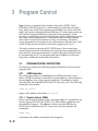
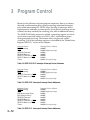
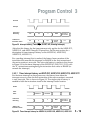
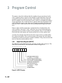
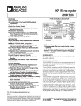
Figure 3.1, on the following page, shows a block diagram of the program
sequencer. Each functional block of the sequencer is discussed is detail in
this chapter.
This chapter discusses both program sequencer logic and the following
instructions used to control program flow:
DO UNTIL
JUMP
CALL
RTS (Return From Subroutine)
RTI (Return From Interrupt)
IDLE
For a complete description of each instruction, refer to Chapter 15,
Instruction Set Reference.
3–1
3 Program Control
DMD BUS
from INSTRUCTION REGISTER
COUNT
STACK
CONDITION CODE
ADDRESS OF JUMP/CALL
FUNCTION FIELD
MUX
ADDRESS OF LAST
INSTRUCTION IN LOOP
&
TERMINATION
CONDITION
CNTR
(Counter)
CE
OUT
LOOP
STACK
STATUS
STACK
MUX
CONDITION
LOGIC
ARITHMETIC
STATUS
(from ALU)
INTERRUPTS
LOOP
COMPARATOR
STATUS
REGISTERS
INTERRUPT
CONTROLLER
PC
STACK
PROGRAM
COUNTER
MUX
INCREMENT
NEXT ADDRESS MUX
PMA BUS
Figure 3.1 Program Sequencer Block Diagram
3–2
from
FI Pin
NEXT
ADDRESS
SOURCE
SELECT
Program Control 3
3.2.1
Next Address Select Logic
While the processor is executing an instruction, the program sequencer
pre-fetches the next instruction. The sequencer’s next address select logic
generates a program memory address (for the pre-fetch) from one of four
sources:
• PC incrementer
• PC stack
• instruction register
• interrupt controller
The next address circuit (shown in Figure 3.1) selects which of these
sources is used, based on inputs from the instruction register, condition
logic, loop comparator and interrupt controller. The next instruction
address is then output on the PMA bus for the pre-fetch.
The PC incrementer is selected as the source of the next address if
program flow is sequential. This is also the case when a conditional jump
or return is not taken and when a DO UNTIL loop terminates. The output
of the PC incrementer is driven onto the PMA bus and is loaded back into
the program counter to begin the next cycle.
The PC stack is used as the source for the next address when a return from
subroutine or return from interrupt is executed. The top stack value is also
used as the next address when returning to the top of a DO UNTIL loop.
The instruction register provides the next address when a direct jump is
taken. The 14-bit jump address is embedded in the instruction word.
The interrupt controller provides the next program memory address when
servicing an interrupt. Upon recognizing a valid interrupt, the processor
jumps to the interrupt vector location corresponding to the active
interrupt request.
Another possible source for the next address is one of the I4-I7 index
registers of DAG2 (Data Address Generator 2), used when a register
indirect jump is executed as in the following instruction:
JUMP (I4);
In this case the program counter (PC) is loaded from DAG2 via the PMA
bus. (Data address generators are described in Chapter 4.)
3–3
3 Program Control
3.2.2
Program Counter & PC Stack
The program counter (PC) is a 14-bit register which always contains the
address of the currently executing instruction. The output of the PC is fed
into a 14-bit incrementer which adds 1 to the current PC value. The output
of the incrementer can be selected by the next address multiplexer to fetch
the next sequential instruction.
Associated with the PC is a 14-bit by 16-word stack that is pushed with the
output of the incrementer when a CALL instruction is executed. The PC
stack is also pushed when a DO UNTIL is executed and when an interrupt
is processed. For interrupts, however, the incrementer is disabled so that
the current PC value (instead of PC+1) is pushed. This allows the current
instruction, which is aborted, to be refetched upon returning from the
interrupt service routine. The pushing and popping of the PC stack occurs
automatically in all of these cases. The stack can also be manually popped
with the POP instruction.
A special instruction is provided for reading (and popping) or writing
(and pushing) the top value of the PC stack. This instruction uses the
pseudo register TOPPCSTACK, described at the end of this chapter.
The output of the next address multiplexer is fed back to the PC, which
normally reloads it at the end of each processor cycle. In the case of a
register indirect jump, however, DAG2 drives the PMA bus with the next
instruction address and the PC is loaded directly from the PMA bus.
3.2.3
Loop Counter & Stack
The counter and count stack provide the program sequencer with a
powerful looping mechanism. The counter is a 14-bit register with
automatic post-decrement capability that controls the flow of program
loops which execute a predetermined number of times. Count values are
14-bit unsigned-magnitude values.
Before entering the loop, the counter (CNTR register) is loaded with the
desired loop count from the lower 14 bits of the DMD bus. The actual loop
count N is loaded, as opposed to N–1. This is due to the operation of the
counter expired (CE) status logic, which tests CE (and automatically postdecrements the counter) at the end of a DO UNTIL loop that uses CE as its
termination condition. CE is tested at the beginning of each processor
cycle and the counter is decremented at the end; therefore CE is asserted
when the counter reaches 1 so that the loop executes N times.
3–4
Program Control 3
The counter may also be tested and automatically decremented by a
conditional jump instruction that tests CE. The counter is not decremented
when CE is checked as part of a conditional return or conditional
arithmetic instruction.
The counter may be read directly over the DMD bus at any time without
affecting its contents. When reading the counter, the upper two bits of the
DMD bus are padded with zeroes.
The count stack is a 14-bit by 4-word stack which allows nesting of loops
by storing temporarily dormant loop counts. When a new value is loaded
into the counter from the DMD bus, the current counter value is
automatically pushed onto the count stack. The count stack is
automatically popped whenever the CE status is tested and is true,
thereby resuming execution of the outer loop (if any). The count stack may
also be popped manually if an early exit from a loop is taken.
There are two exceptions to the automatic pushing of the count stack. A
counter load from the DMD bus does not cause a count stack push if there
is no valid value in the counter, because a stack location would be wasted
on the invalid counter value. There is no valid value in the counter after a
system reset and also after the CE condition is tested when the count stack
is empty. The count stack empty status bit in the SSTAT register indicates
when the stack is empty.
The second exception is provided explicitly by the special purpose syntax
OWRCNTR (overwrite counter). Writing a value to OWRCNTR
overwrites the counter with the new value, and nothing is pushed onto
the count stack. OWRCNTR cannot be read (i.e. used as a source register),
and must not be written in the last instruction of a DO UNTIL loop.
3.2.4
Loop Comparator & Stack
The DO UNTIL instruction initiates a zero-overhead loop using the loop
comparator and loop stack of the program sequencer.
On every processor cycle, the loop comparator compares the next address
generated by the program sequencer to the address of the last instruction
of the loop (which is embedded in the DO UNTIL instruction). The
address of the first instruction in the loop is maintained on the top of the
PC stack. When the last instruction in the loop is executed the processor
conditionally jumps to the beginning of the loop, eliminating the
branching overhead otherwise incurred in loop execution.
3–5
3 Program Control
The loop stack stores the last instruction addresses and termination
conditions of temporarily dormant loops. Up to four levels can be stored.
The only extra cycle associated with the nesting of DO UNTIL loops is the
execution of the DO UNTIL instruction itself, since the pushing and
popping of all stacks associated with the looping hardware is automatic.
When using the counter expired (CE) status as the termination condition
for the loop, an additional cycle is required for the initial loading of the
counter. Table 3.1 shows the termination conditions that can be used with
DO UNTIL.
Syntax
Status Condition
True If:
EQ
NE
LT
GE
LE
GT
AC
NOT AC
AV
NOT AV
MV
NOT MV
NEG
POS
CE
FOREVER
Equal Zero
Not Equal Zero
Less Than Zero
Greater Than or Equal Zero
Less Than or Equal Zero
Greater Than Zero
ALU Carry
Not ALU Carry
ALU Overflow
Not ALU Overflow
MAC Overflow
Not MAC Overflow
X Input Sign Negative
X Input Sign Positive
Counter Expired
Always
AZ = 1
AZ = 0
AN .XOR. AV = 1
AN .XOR. AV = 0
(AN .XOR. AV) .OR. AZ = 1
(AN .XOR. AV) .OR. AZ = 0
AC = 1
AC = 0
AV = 1
AV = 0
MV = 1
MV = 0
AS = 1
AS = 0
Table 3.1 DO UNTIL Termination Condition Logic
When a DO UNTIL instruction is executed, the 14-bit address of the last
instruction and a 4-bit termination condition (both contained in the DO
UNTIL instruction) are pushed onto the 18-bit by 4-word loop stack.
Simultaneously, the PC incrementer output is pushed onto the PC stack.
Since the DO UNTIL instruction is located just before the first instruction
of the loop, the PC stack then contains the first loop instruction address,
and the loop stack contains the last loop instruction address and
termination condition. The non-empty state of the loop stack activates the
loop comparator which compares the address on top of the loop stack
with the address of the next instruction. When these two addresses are
equal, the loop comparator notifies the next address source selector that
the last instruction in the loop will be executed on the next cycle.
3–6
Program Control 3
At this point, there are three possible results depending on the type of
instruction at the end of the loop. Case 1 illustrates the most typical
situation. Cases 2 and 3 are also allowed but involve greater program
complexity for proper execution.
Case 1
If the last instruction in the loop is not a jump, call, return, or idle, the
next address circuit will select the next address based on the
termination condition stored on the top of the loop stack. If the
condition is false, the top address on the PC stack is selected, causing
a fetch of the first instruction of the loop. If the termination condition
is true, the PC incrementer is chosen, causing execution to fall out of
the loop. The loop stack, PC stack, and counter stack (if being used)
are then popped.
(Note that conditional arithmetic instructions execute based on the
condition explicitly stated in the instruction, whereas the loop
sequencing is controlled by the (implicit) termination condition
contained on top of the stack.)
Case 2
If the last instruction in the loop is a jump, call, or return, the
explicitly stated instruction takes precedence over the implicit
sequencing of the loop. If the condition in the instruction is false,
normal loop sequencing takes place as described for Case 1.
If the condition in the instruction is true, however, program control
transfers to the jump/call/return address. Any actions that would
normally occur upon an end-of-loop detection do not take place:
fetching the first instruction of the loop, falling out of the loop and
popping the loop stack, PC stack, and counter stack, or decrementing
the counter.
(Note that for a return instruction, control is passed back to the top of
the loop since the PC stack contains the beginning address of the
loop.)
Case 3
If the last instruction in the loop is an IDLE, program flow is
controlled by the IDLE instruction rather than the loop. When the
IDLE instruction is executed, the processor enters a low-power waitfor-interrupt state. When the processor is interrupted, loop execution
terminates and program execution continues with the first instruction
following the loop.
3–7
3 Program Control
Note: Caution is required when ending a loop with a JUMP, CALL,
RETURN, or IDLE instruction, or when making a premature exit from a
loop. Since none of the loop sequencing mechanisms are active while the
jump/call/return is being performed, the loop, PC, and counter stacks are
left with the looping information (since they are not popped). In this
situation, a manual pop of each of the relevant stacks is required to restore
the correct state of the processor. A subroutine call poses this problem
only when it is the last instruction in a loop; in such cases, the return
causes program flow to transfer to the instruction just after the loop. Calls
within a loop that are not the last instruction operate as in Case 1.
The only restriction concerning DO UNTIL loops is that nested loops
cannot terminate on the same instruction. Since the loop comparator can
only check for one loop termination at a time, falling out of an inner loop
by incrementing the PC would go beyond the end address of the outer
loop if they terminated on the same instruction.
3.3
PROGRAM CONTROL INSTRUCTIONS
The following sections describe the primary instructions used to control
program flow.
3.3.1
JUMP Instruction
The 14-bit jump address is embedded in the JUMP instruction word.
When a JUMP instruction is decoded, the jump address is input directly to
the next address mux of the program sequencer. The address is driven
onto the PMA bus and fed back to the PC for the next cycle. The following
instruction, for example,
JUMP fir_start;
jumps to the address of the label fir_start.
3.3.1.1 Register Indirect JUMPs
In this case of register indirect jumps, the jump address is supplied by one
of the I registers of DAG2 (I4, I5, I6, or I7). (Data address generators are
described in Chapter 4.) The address is driven onto the PMA bus by
DAG2, and is loaded into the PC on the next cycle. For example, the
instruction
JUMP (I4);
will jump to the address contained in the I4 register.
3–8
Program Control 3
3.3.2
CALL Instruction
The CALL instruction executes in a similar fashion as the JUMP
instruction. The address of the subroutine is embedded in the CALL
instruction word and, once extracted from the instruction register, is fed
back the PC for the next cycle. In addition, the current value of the
program counter is incremented and pushed onto the PC stack. Upon
return from the subroutine, the PC stack is popped into the program
counter and execution resumes with the instruction following the CALL.
3.3.3
DO UNTIL Loops
The most common form of a DO UNTIL loop uses the counter register
(CNTR) as a loop iteration counter. When the counter is used to control
loop iteration, CE (counter expired) must be used as the DO UNTIL
termination condition. A simple example of this type of loop is as follows:
L0=10;
I0=^data_buffer;
M0=1;
CNTR=10;
{setup circular buffer length register}
{load pointer with first address of}
{circular buffer}
{setup modify register for pointer increment}
{load counter with circular buffer length}
DO loop UNTIL CE; {repeat loop until counter expired}
DM(I0,M0)=0;
{initialize/clear circular buffer}
...any instruction...
loop: ...any instruction...
When the
CNTR=10;
instruction is executed, prior to entering the loop, the counter is loaded via
the DMD bus. Any previously existing count would be simultaneously
pushed onto the count stack; this push operation is omitted if the counter
is empty. The
DO loop UNTIL CE;
instruction itself only sets up the conditions for looping; no other
operation occurs while the instruction is executed. This occurs only once,
at the beginning of the first time through the loop.
3–9
3 Program Control
Execution of the DO UNTIL instruction pushes the address of the
instruction immediately following the DO UNTIL onto the PC stack (by
pushing the incremented PC). On the same cycle, the loop stack is pushed
with the address of the end-of-loop instruction and the termination
condition.
As execution continues within the loop, the loop comparator checks each
instruction’s address against the address of the loop’s last instruction.
Until that address is reached, normal execution continues.
Each time the end of the loop is reached, the loop comparator determines
that the currently executing instruction is the last in the loop. This affects
the next address select logic of the program sequencer: instead of using
the incremented PC for the next address, the loop termination condition is
evaluated. If the termination condition is false, execution continues with
the first instruction of the loop (the top of the PC stack is taken as the next
address). Note that the PC and loop stacks are not popped, only read.
On the final pass through the loop, the termination condition is true. The
PC stack is popped and execution continues with the instruction
immediately following the last instruction of the loop. The loop stack and
count stack are also popped on this cycle.
3.3.4
IDLE Instruction
The IDLE instruction causes the processor to wait indefinitely in a low
power state until an interrupt occurs. When an unmasked interrupt
occurs, it is serviced; execution then continues with the instruction
following the IDLE instruction.
3.3.4.1 Slow IDLE
An enhanced version of the IDLE intruction allows the processor’s
internal clock signal to be slowed, further reducing power consumption.
The reduced clock frequency, a programmable fraction of the normal clock
rate, is specified by a selectable divisor given in the IDLE instruction. The
format of the instruction is
IDLE (n);
where n = 16, 32, 64, or 128. This instruction keeps the processor fully
functional, but operating at the slower clock rate. While it is in this state,
the processor’s other internal clock signals, such as SCLK, CLKOUT, and
timer clock, are reduced by the same ratio. The default form of the
instruction, when no clock divisor is given, is the standard IDLE
instruction.
3 – 10
Program Control 3
When the IDLE (n) instruction is used, it effectively slows down the
processor’s internal clock and thus its response time to incoming
interrupts. The one-cycle interrupt response time of the standard idle state
is increased by n, the clock divisor. When an enabled interrupt is received,
the processor will remain in the idle state for up to a maximum of n
processor cycles before resuming normal operation (n = 16, 32, 64, or 128).
When the IDLE (n) instruction is used in systems that have an externally
generated serial clock (SCLK), the serial clock rate may be faster than the
processor’s reduced internal clock rate. Under these conditions, interrupts
must not be generated at a faster rate than can be serviced, due to the
additional time the processor takes to come out of the idle state (a
maximum of n processor cycles).
3.4
INTERRUPTS
The program sequencer’s interrupt controller responds to interrupts by
shifting control to the instruction located at the appropriate interrupt
vector address. Tables 3.2–3.7 show the interrupts and associated vector
addresses for each processor of the ADSP-2100 family. (Note that SPORT1
can be configured as either a serial port or as a collection of control pins
including two external interrupt inputs, IRQ0 and IRQ1. See Chapter 5,
“Serial Ports,” for more information about the configuration of SPORT1.)
The interrupt vector locations are spaced four program memory locations
apart—this allows short interrupt service routines to be coded in place,
with no jump to the service routine required. For interrupt service
routines with more than four instructions, however, program control must
be transferred to the service routine by means of a jump instruction placed
at the interrupt vector location.
After an interrupt has been serviced, an RTI (Return From Interrupt)
instruction returns control to the main program by popping the top value
on the PC stack into the PC; the status stack is also popped to restore the
previous processor state.
Interrupts can also be forced under software control; see the discussion of
the IFC register below.
3 – 11
3 Program Control
Because of the efficient stack and program sequencer, there is no latency
(beyond synchronization delay) when processing unmasked interrupts,
even when interrupting DO UNTIL loops. Nesting of interrupts allows
higher-priority interrupts to interrupt any lower-priority interrupt service
routines that may currently be executing, also with no additional latency.
The ADSP-2100 family processors include a secondary register set which
can be used to provide a fresh set of ALU, MAC, and Shifter registers
during interrupt servicing. This feature allows single-cycle context
switching. Use of the secondary registers is described in the “Mode Status
Register (MSTAT)” section of this chapter.
Interrupt Source
RESET startup
IRQ2
SPORT0 Transmit
SPORT0 Receive
SPORT1 Transmit or IRQ1
SPORT1 Receive or IRQ0
Timer
Interrupt Vector Address
0x0000
0x0004 (highest priority)
0x0008
0x000C
0x0010
0x0014
0x0018 (lowest priority)
Table 3.2 ADSP-2101/2115 Interrupts & Interrupt Vector Addresses
Interrupt Source
RESET startup
IRQ2
SPORT1 Transmit or IRQ1
SPORT1 Receive or IRQ0
Timer
Interrupt Vector Address
0x0000
0x0004 (highest priority)
0x0010
0x0014
0x0018 (lowest priority)
Table 3.3 ADSP-2105 Interrupts & Interrupt Vector Addresses
Interrupt Source
RESET startup
IRQ2
HIP Write (from Host)
HIP Read (to Host)
SPORT0 Transmit
SPORT0 Receive
SPORT1 Transmit or IRQ1
SPORT1 Receive or IRQ0
Timer
Interrupt Vector Address
0x0000
0x0004 (highest priority)
0x0008
0x000C
0x0010
0x0014
0x0018
0x001C
0x0020 (lowest priority)
Table 3.4 ADSP-2111 Interrupts & Interrupt Vector Addresses
3 – 12
Program Control 3
Interrupt Source
RESET startup (or powerup w/PUCR=1)
Powerdown (non-maskable)
IRQ2
HIP Write (from Host)
HIP Read (to Host)
SPORT0 Transmit
SPORT0 Receive
Software Interrupt 1
Software Interrupt 2
SPORT1 Transmit or IRQ1
SPORT1 Receive or IRQ0
Timer
Interrupt Vector Address
0x0000 (highest priority)
0x002C
0x0004
0x0008
0x000C
0x0010
0x0014
0x0018
0x001C
0x0020
0x0024
0x0028 (lowest priority)
Table 3.5 ADSP-2171 Interrupts & Interrupt Vector Addresses
Interrupt Source
RESET startup (or powerup w/PUCR=1)
Powerdown (non-maskable)
IRQ2
IRQL1 (level-sensitive)
IRQL0 (level-sensitive)
SPORT0 Transmit
SPORT0 Receive
IRQE (edge-sensitive)
Byte DMA Interrupt
SPORT1 Transmit or IRQ1
SPORT1 Receive or IRQ0
Timer
Interrupt Vector Address
0x0000 (highest priority)
0x002C
0x0004
0x0008
0x000C
0x0010
0x0014
0x0018
0x001C
0x0020
0x0024
0x0028 (lowest priority)
Table 3.6 ADSP-2181 Interrupts & Interrupt Vector Addresses
Interrupt Source
RESET startup (or powerup w/PUCR=1)
Powerdown (non-maskable)
IRQ2
HIP Write (from Host)
HIP Read (to Host)
SPORT0 Transmit
SPORT0 Receive
Analog (DAC) Transmit
Analog (ADC) Receive
SPORT1 Transmit or IRQ1
SPORT1 Receive or IRQ0
Timer
Interrupt Vector Address
0x0000 (highest priority)
0x002C
0x0004
0x0008
0x000C
0x0010
0x0014
0x0018
0x001C
0x0020
0x0024
0x0028 (lowest priority)
Table 3.7 ADSP-21msp58/59 Interrupts & Interrupt Vector Addresses
3 – 13
3 Program Control
3.4.1
Interrupt Servicing Sequence
When an interrupt request occurs, it is latched while the processor finishes
executing the current instruction. The interrupt request is then compared
with the interrupt mask register, IMASK, by the interrupt controller.
If the interrupt is not masked, the program sequencer pushes the current
value of the program counter (which contains the address of the next
instruction) onto the PC stack—this allows execution to continue, after the
interrupt is serviced, with the next instruction of the main program. The
program sequencer also pushes the current values of the ASTAT, MSTAT,
and IMASK registers onto the status stack. ASTAT, MSTAT and IMASK
are stored in this order, with the MSB of ASTAT first, and so on. When
IMASK is pushed, it is automatically reloaded with a new value that
determines whether or not interrupt nesting is allowed (based on the
value of the interrupt nesting enable bit in ICNTL).
The processor then executes a NOP while simultaneously fetching the
instruction located at the interrupt vector address. Upon return from the
interrupt service routine, the PC and status stacks are popped and
execution resumes with the next instruction of the main program.
3.4.2
Configuring Interrupts
The following registers are used to configure interrupts:
• ICNTL—Determines whether interrupts can be nested and configures
the external interrupts IRQ2, IRQ1, IRQ0 as edge-sensitive or levelsensitive
• IMASK—Enables or disables (i.e. masks) each individual interrupt (both
external and internal).
• IFC—Forces an interrupt or clears a pending edge-sensitive interrupt.
The IRQ2, IRQ1, IRQ0 interrupts may be either edge-sensitive or levelsensitive, as selected in the ICNTL register. The ADSP-2181 has three
additional interrupt pins: IRQE, IRQL1, and IRQL2. The IRQE input is
edge-sensitive, while the IRQL1 and IRQL2 inputs are level-sensitive.
For edge-sensitive IRQx interrupts, an interrupt request is latched
internally whenever a falling edge (high-to-low transition) occurs at the
input pin. The latch remains set until the interrupt is serviced; it is then
automatically cleared. A pending edge-sensitive interrupt can also be
cleared in software by setting the corresponding clear bit in the IFC
register.
3 – 14
Program Control 3
Edge-sensitive interrupt inputs generally require less external hardware
than level-sensitive inputs, and allow signals such as sampling-rate clocks
to be used as interrupts.
A level-sensitive interrupt must remain asserted until the interrupt is
serviced. The interrupting device must then deassert the interrupt request
so that the interrupt is not serviced again. Level-sensitive inputs, however,
allow many interrupt sources to use the same input by combining them
logically to produce a single interrupt request. Level-sensitive interrupts
are not latched.
Your program can also determine whether or not interrupts can be nested.
In non-nesting mode, all interrupt requests are automatically masked out
when an interrupt service routine is entered. In nesting mode, the
processor allows higher-priority interrupts to be recognized and serviced.
There are two levels of masking for the Host Interface Port (HIP)
interrupts of the ADSP-2111, ADSP-2171, and ADSP-21msp58/59. The
memory-mapped HMASK register configures masking out the generation
of individual read or write interrupts for each HIP data register. The
IMASK register can be set to mask or enable the servicing of all HIP read
interrupts or all HIP write interrupts. Both IMASK and HMASK must be
set for HDR interrupts. See Chapter 7, “Host Interface Port,” for details.
3.4.2.1 Interrupt Control Register (ICNTL)
ICNTL is a 5-bit register that configures the external interrupt requests
(IRQx ) of each processor. All bits in ICNTL are undefined after a
processor reset. The bit definitions for each processor’s ICNTL register are
given in Appendix E, “Control/Status Registers.”
ICNTL contains an IRQx sensitivity bit for each external interrupt. The
sensitivity bits determine whether a given interrupt input is edge- or levelsensitive (0 = level-sensitive, 1 = edge-sensitive). There are no sensitivity
bits for internally generated interrupts.
The interrupt nesting enable bit (bit 4) in ICNTL determines whether
nesting of interrupt service routines is allowed.
When the value of ICNTL is changed, there is a one cycle latency before
the change in interrupt configuration.
3 – 15
3 Program Control
3.4.2.2 Interrupt Mask Register (IMASK)
Each bit of the IMASK register enables or disables the servicing of an
individual interrupt. Specific bit definitions for each processor’s IMASK
register are given in Appendix E, “Control/Status Registers.” The mask
bits are positive sense: 0=masked, 1=enabled. IMASK is set to zero upon a
processor reset.
On the ADSP-2171, ADSP-2181, and ADSP-21msp58/59 processors, all
interrupts are automatically disabled for one instruction cycle following
the execution of an instruction that modifies IMASK. This does not affect
serial port autobuffering or DMA transfers.
If an edge-sensitive interrupt request signal occurs when the interrupt is
masked, the request is latched but not serviced; the interrupt can then be
recognized in software and serviced later.
The contents of IMASK are automatically pushed onto the status stack
when entering an interrupt service routine and popped back when
returning from the routine. The configuration of IMASK upon entering the
interrupt service routine is determined by the interrupt nesting enable bit
(bit 4) of ICNTL; it may be altered, though, as part of the interrupt service
routine itself.
When nesting is disabled, all interrupt levels are masked automatically
(IMASK set to zero) when an interrupt service routine is entered.
When nesting is enabled, IMASK is set so that only equal and lower
priority interrupts are masked; higher priority interrupts remain
configured as they were prior to the interrupt. This is shown graphically,
for the ADSP-2101, in Table 3.8.
The interrupt nesting enable bit (in ICNTL) determines the state of IMASK
upon entering the interrupt, as shown in Table 3.8.
3 – 16
Program Control 3
ICNTL Interrupt Nesting Enable bit = 0 (nesting disabled)
Interrupt
IMASK contents before IMASK contents entering
level serviced
(pushed on stack)
interrupt service routine
0 (low)
1
2
3
4
5 (high)
ijklmn
ijklmn
ijklmn
ijklmn
ijklmn
ijklmn
000000
000000
000000
000000
000000
000000
ICNTL Interrupt Nesting Enable bit = 1 (nesting enabled)
Interrupt
IMASK contents before IMASK contents entering
level serviced
(pushed on stack)
interrupt service routine
0 (low)
1
2
3
4
5 (high)
ijklmn
ijklmn
ijklmn
ijklmn
ijklmn
ijklmn
ijklm0
ijkl00
ijk000
ij0000
i00000
000000
(“ijklmn” represents any pattern of ones and zeroes)
Table 3.8 IMASK Entering Interrupt Service Routines (ADSP-2101 example)
3.4.2.3 Global Enable/Disable for Interrupts
Global interrupt enable and disable instructions are available on the
ADSP-2171, ADSP-2181, and ADSP-21msp58/59 processors:
ENA INTS;
DIS INTS;
Interrupts are enabled by default after reset. The DIS INTS instruction
causes all interrupts (including powerdown) to be masked out regardless
of the contents of IMASK. The ENA INTS instruction allows all
unmasked interrupts to be serviced again.
Disabling interrupts does not affect serial port autobuffering.
3 – 17
3 Program Control
3.4.2.4 Interrupt Force & Clear Register (IFC)
IFC is a write-only register that allows the forcing and clearing of edgesensitive interrupts in software. An interrupt is forced or cleared under
program control by setting the force or clear bit corresponding to the
desired interrupt. After the force or clear bit is set, there is one cycle of
latency before the interrupt is actually forced or cleared (except for the
timer interrupt on the ADSP-2101/2105/2111/2115 processors).
Edge-sensitive interrupts can be forced by setting the appropriate force bit
in IFC. This causes the interrupt to be serviced once, unless masked. An
external interrupt must be edge-sensitive (as determined by ICNTL) to be
forced. The timer, SPORT, and analog ADC/DAC interrupts also behave
like edge-sensitive interrupts and can be masked, cleared and forced.
Pending edge-sensitive interrupts can be cleared by setting the
appropriate clear bit in IFC. Edge-triggered interrupts are cleared
automatically when the corresponding interrupt service routine is called.
Specific bit definitions for each processor’s IFC register are given in
Appendix E, “Control/Status Registers.” The IFC registers of the ADSP2111, ADSP-2171, and ADSP-21msp58 processors do not include force/
clear bits for Host Interface Port interrupts; HIP interrupts cannot be
forced or cleared in software.
3.4.3
Interrupt Latency
For the timer, IRQx, SPORT, HIP, and analog interface interrupts, the
latency from when an interrupt occurs to when the first instruction of the
service routine is executed is at least three full cycles. This is shown in
Figure 3.2. Two cycles are required to synchronize the interrupt internally,
assuming that setup and hold times are met (for the IRQx input pins).
Since interrupts are only serviced on instruction boundaries, the
instruction(s) executed during these two cycles must be fully completed,
including any extra cycles inserted due to Bus Request/Bus Grant or
memory wait states, before execution continues.
The third cycle of latency is needed to fetch the first instruction stored at
the interrupt vector location. During this cycle, the processor executes a
NOP instead of the instruction that would normally have been executed.
On the next cycle, execution continues at the first instruction of the
interrupt service routine. The address of the aborted instruction is pushed
onto the PC stack; it will be fetched when the interrupt service routine is
completed.
3 – 18
Program Control 3
CLKOUT
Interrupt
Instruction
Executing
Address for
Instruction Fetch
n–2
n–1
n–1
n
n
n+1
NOP
interrupt
vector i
1st instr of
serv routine
i+1
x, SPORT, HIP, & Analog Interrupts)
Figure 3.2 Interrupt Latency (Timer, IRQ
IRQx
(Note that this latency for the timer interrupt only applies for the ADSP-2171,
ADSP-2181, and ADSP-21msp58/59 processors. See the next section for a
description of timer interrupt latency on the ADSP-2101, ADSP-2105,
ADSP-2115, ADSP-2111.)
For a pending interrupt that is masked, the latency from execution of the
instruction that unmasks the interrupt (in IMASK) to the first instruction of
the service routine is one cycle. This one-cycle latency is similar to that shown
in Figure 3.3 for the timer interrupt of the ADSP-2101/2105/2111/2115, with
the “n” instruction executing being the instruction that writes to IMASK (to
unmask the interrupt).
3.4.3.1 Timer Interrupt Latency on ADSP-2101, ADSP-2105, ADSP-2115, ADSP-2111
For the timer interrupt on these processors, the latency from when the
interrupt occurs to when the first instruction of the service routine is executed
is only one cycle. This is shown in Figure 3.3. The single cycle of latency is
needed to fetch the instruction stored at the interrupt vector location.
CLKIN
Timer
Value
Instruction
Executing
Address for
Instruction Fetch
tcount=1
tcount=0
n
n+1
NOP
interrupt
vector i
1st instr of
serv routine
i+1
Figure 3.3 Timer Interrupt Latency for ADSP-2101, ADSP-2105, ADSP-2115, ADSP-2111
3 – 19
3 Program Control
3.5
STATUS REGISTERS & STATUS STACK
Processor status and mode bits are maintained in internal registers which
can be independently read and written over the DMD bus. These registers
are:
ASTAT
SSTAT
MSTAT
ICNTL
IMASK
IFC
Arithmetic status register
Stack status register(read-only)
Mode status register
Interrupt control register
Interrupt mask register
Interrupt force/clear register(write-only)
The interrupt-configuring status registers are described in the previous
section. ASTAT, SSTAT, and MSTAT are discussed in the following
sections.
The current ASTAT, MSTAT, and IMASK values are pushed onto the
status stack when the processor responds to an interrupt; they are popped
upon return from the interrupt service routine (with the RTI instruction).
The depth of the stack varies from processor to processor. In each case,
sufficient stack depth is provided to accommodate nesting of all
interrupts.
3.5.1
Arithmetic Status Register (ASTAT)
ASTAT is eight bits wide and holds the status information generated by
the computational blocks of the processor. The individual bits of ASTAT
are defined as shown in Figure 3.4. The bits which express a particular
condition (AZ, AN, AV, AC, MV) are all positive sense (1=true, 0=false).
7
6
5
4
3
2
1
0
0
0
0
0
0
0
0
0
SS
MV AQ AS
AC AV AN AZ
ALU Result Zero
ALU Result Negative
ALU Overflow
ALU Carry
ALU X Input Sign
ALU Quotient
MAC Overflow
3 – 20
Shifter Input Sign
Figure 3.4 ASTAT Register
Program Control 3
Each of the bits is automatically updated when a new status is generated
by an arithmetic instruction. Each bit is affected only by a subset of
arithmetic operations, as defined by the following table:
Status Bit
AZ, AN, AV, AC
AS
AQ
MV
SS
Updated by
Any ALU operation except DIVS, DIVQ
ALU absolute value operation (ABS)
ALU divide operations (DIVS, DIVQ)
Any MAC operation except saturate MR (SAT MR)
Shifter EXP operation
Arithmetic status is latched into ASTAT at the end of the cycle in which it
was generated, and cannot be used until the next cycle.
Loading any ALU, MAC, or Shifter input or output registers directly from
the DMD bus does not affect any of the arithmetic status bits. Executing
the ALU instruction PASS sets the AZ and AN bits for a given X or Y
operand and clears AC.
3.5.2
Stack Status Register (SSTAT)
The SSTAT register is eight bits wide and holds information about the four
processor stacks. The individual bits of SSTAT are defined as shown in
Figure 3.5. All of the bits are positive sense (1=true, 0=false).
7
6
5
4
3
2
1
0
0
1
0
1
0
1
0
1
PC Stack Empty
PC Stack Overflow
Count Stack Empty
Count Stack Overflow
Status Stack Empty
Status Stack Overflow
Loop Stack Empty
Loop Stack Overflow
Figure 3.5 SSTAT Register (Read-Only)
3 – 21
3 Program Control
The empty status bits indicate that the number of pop operations for the
stack is greater than or equal to the number of push operations that have
occurred since the last processor reset. The overflow status bits indicate
that the number of push operations for the stack has exceeded the number
of pop operations, by an amount that is greater than the total depth of the
stack. When this occurs, the values most recently pushed will be missing
from the stack—older stack values are considered more important than
new.
Since a stack overflow represents a permanent loss of information, the
stack overflow status bits “stick” once they are set, and subsequent pop
operations have no effect on them. In this situation, then, it is possible to
have both the stack empty and stack overflow bits set for a given stack.
Assume, for example, that the four-location count stack is overflowed by
five successive pushes. Five successive pops will restore the stack empty
condition, but will not clear the overflow condition. The processor must be
reset to clear the stack overflow status.
3.5.3
Mode Status Register (MSTAT)
The MSTAT register determines the operating mode of the processor. The
individual bits of MSTAT are defined as shown in Figure 3.6.
6
5
4
3
2
1
0
0
0
0
0
0
0
0
Data Register Bank Select
0 = primary, 1 = secondary
Bit Reverse Mode Enable (DAG1)
ALU Overflow Latch Mode Enable
AR Saturation Mode Enable
MAC Result Placement
0 = fractional, 1 = integer
Timer Enable
Go Mode Enable
Figure 3.6 MSTAT Register
3 – 22
Program Control 3
MSTAT can be modified by writing a new value to it with a MOVE
instruction. Unlike the other status registers, MSTAT can also be altered
with the Mode Control instruction (ENA, DIS). The Mode Control
instruction provides a high-level, self-documenting method of configuring
the processors’ operating modes. Refer to the description of the Mode
Control instruction in Chapter 15, “Instruction Set Reference,” for further
details.
To enable the bit reverse mode, for example, the following instruction
could be used:
ENA BIT_REV;
The bit-reverse mode, when enabled, bitwise reverses all addresses
generated by data address generator 1 (DAG1). This is useful for
reordering the input or output data of an FFT algorithm.
The ADSP-2100 family processors include a secondary register set which
can be used to provide a fresh set of ALU, MAC, and Shifter registers at
any time, for example during execution of a subroutine. The data register
bank select bit of MSTAT determines which set of data registers is active
(0=primary, 1=secondary). The secondary register set duplicates all of the
input and result registers of the computation units, ALU, MAC, and
Shifter:
AX0
AX1
AY0
AY1
AF
AR
MX0
MX1
MY0
MY1
MF
MR0
MR1
MR2
SI
SE
SB
SR1
SR0
The following mode control instruction, for example, switches from the
processor’s primary register set to its secondary register set:
ENA SEC_REG;
while the following instruction switches back to the primary register set:
DIS SEC_REG;
3 – 23
3 Program Control
The ALU overflow latch mode causes the AV status bit to “stick” once it is
set. In this mode, AV will be set by an overflow and will remain set even if
subsequent ALU operations do not generate overflows. AV can then be
cleared only by writing a zero into it.
AR saturation mode, when enabled, causes AR to be saturated to the
maximum positive (0x7FFF) or negative (0x8000) values whenever an
ALU overflow occurs.
The MAC result placement mode determines whether the multiplier
operates in integer or fractional format. This mode is discussed in Chapter
2, “Computational Units.”
Setting the timer enable bit causes the timer to begin decrementing.
Clearing this bit halts the timer.
Enabling GO mode allows the processor to continue executing instructions
from internal program memory during a bus grant. The processor will
halt, waiting for the buses to be released, only when an access of external
memory is required. When GO mode is disabled, the processor always
halts during bus grant.
3.6
CONDITIONAL INSTRUCTIONS
The condition logic circuit of the program sequencer determines whether a
conditional instruction is executed, for example a jump, call, or arithmetic
operation. It also controls implicit loop sequencing operations based upon
the loop continuation condition on top of the loop stack. The condition
logic takes raw status information from ASTAT and the down counter and
derives a set of sixteen composite status conditions.
The status conditions and corresponding assembly language syntax are
listed in Table 3.9. These status conditions are used with the IF condition
clause available on some instructions. In addition, the status of the FI pin
(Flag In) can also be used as a condition for JUMP and CALL instructions.
3 – 24
Program Control 3
Syntax
EQ
NE
LT
GE
LE
GT
AC
NOT AC
AV
NOT AV
MV
NOT MV
NEG
POS
NOT CE
FLAG_IN*
NOT FLAG_IN*
Status Condition
Equal Zero
Not Equal Zero
Less Than Zero
Greater Than or Equal Zero
Less Than or Equal Zero
Greater Than Zero
ALU Carry
Not ALU Carry
ALU Overflow
Not ALU Overflow
MAC Overflow
Not MAC Overflow
X Input Sign Negative
X Input Sign Positive
Not Counter Expired
FI pin
Not FI pin
True If:
AZ = 1
AZ = 0
AN .XOR. AV = 1
AN .XOR. AV = 0
(AN .XOR. AV) .OR. AZ = 1
(AN .XOR. AV) .OR. AZ = 0
AC = 1
AC = 0
AV = 1
AV = 0
MV = 1
MV = 0
AS = 1
AS = 0
—
Last sample of FI pin = 1
Last sample of FI pin = 0
* Only available on JUMP and CALL instructions.
Table 3.9 IF Condition Logic
3.7
TOPPCSTACK
A special version of the Register-to-Register Move instruction, Type 17, is
provided for reading (and popping) or writing (and pushing) the top
value of the PC stack. The normal POP PC instruction does not save the
value popped from the stack, so to save this value into a register you must
use the following special instruction:
reg = TOPPCSTACK;
{pop PC stack into reg}
{“toppcstack” may also be
lowercase}
The PC stack is also popped by this instruction, after a one-cycle delay.
A NOP should usually be placed after the special instruction, to allow the
pop to occur properly:
reg = TOPPCSTACK;
NOP;
{allow pop to occur correctly}
3 – 25
3 Program Control
There is no standard PUSH PC stack instruction. To push a specific value
onto the PC stack, therefore, use the following special instruction:
TOPPCSTACK = reg;
{push reg contents onto PC stack}
The stack is pushed immediately, in the same cycle.
Examples:
AX0 = TOPPCSTACK;
NOP;
{pop PC stack into AX0}
TOPPCSTACK = I7;
{push contents of I7 onto PC stack}
Only the following registers may be used in the special TOPPCSTACK
instructions:
ALU, MAC,
& Shifter
Registers
AX0
AX1
MX0
MX1
AY0
AY1
MY0
MY1
AR
MR0
MR1
MR
SI
SE
SR0
SR1
DAG
Registers
I0
I4
I1
I5
I2
I6
I3
I7
M0
M4
M1
M5
M2
M6
M3
M7
L0
L4
L1
L5
L2
L6
L3
L7
The Type 17 Register Move instruction is described in Chapter 15,
Instruction Set Reference. Note that TOPPCSTACK may not be used as a
register in any other instruction type!
3 – 26
Program Control 3
3.7.1
TOPPCSTACK Restrictions
There are several restrictions on the use of the special TOPPCSTACK
instructions, as described below.
1.) The pop and read TOPPCSTACK instruction may not be placed
directly before an RTI instruction (return from interrupt). A NOP
must be inserted in between:
reg = TOPPCSTACK;
NOP;
{allow pop to occur correctly}
RTI;
{another pop happens automatically}
2.) The pop and read TOPPCSTACK instruction may not be the last or
next-to-last instruction in a Do Until loop. Neither instruction 1 nor
instruction 2 may be the pop/read TOPPCSTACK instruction in the
following code:
DO loop UNTIL CE;
loop:
AX0=DM(I5,M5);
...
instruction 2;
instruction 1;
3.) There must be an equal number of pushes and pops within any Do
Until loop, including any normal POP PC instructions as well as the
special TOPPCSTACK pop/read and push/write instructions.
4.) Several restrictions exist in relation to the RTS (return from
subroutine), RTI (return from interrupt routine), and POP PC
instructions. If instruction 3 in the following sequence is an RTS, RTI,
or POP PC,
instruction 1;
instruction 2;
3 – 27
Program Control 3
instruction 3; {if this is an RTS, RTI, or POP PC … }
then the following restrictions must be observed:
- instruction 2 may not be either the pop/read or push/write TOPPCSTACK instruction.
- If instruction 3 is also the last instruction of a Do Until loop, then instruction 1 may not be the
push/write TOPPCSTACK instruction.
3-28