1
Programming Model
12.1
12
OVERVIEW
From a programming standpoint, the ADSP-21xx processors consist of
three computational units, two data address generators, and a program
sequencer, plus on-chip peripherals and memory that vary with each
processor. Almost all operations using these architectural components
involve one or more registers—to store data, to keep track of values such
as pointers, or to specify operating modes, for example.
Internal registers hold data, addresses, control information or status
information. For example, AX0 stores an ALU operand (data); I4 stores a
DAG2 pointer (address); ASTAT contains status flags from arithmetic
operations; and fields in the Wait State register control the number of wait
states for different zones of external memory.
There are two types of accesses for registers. Dedicated registers such as
MX0 and IMASK can be read and written explicitly in assembly language.
For example:
MX0=1234;
IMASK=0xF;
Memory-mapped registers—the System Control Register, Wait State
Control Register, timer registers, SPORT registers, etc.—are accessed by
reading and writing the corresponding data memory locations. For
example, this code clears the Wait State Control Register, which is mapped
to data memory location 0x3FFE:
AX0=0;
DM(0x3FFE)=AX0;
(AX0 is used to hold the constant 0 because there is no instruction to write
an immediate data value to memory using an immediate address.)
12 – 1
12 Programming Model
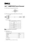
The ADSP-21xx registers are shown in Figure 12.1. Not all of these registers
are available on every processor. The registers are grouped by function: data
address generators (DAGs), program sequencer, computational units (ALU,
MAC and shifter), bus exchange (PX), memory interface, timer, SPORTs, host
interface and DMA interfaces.
12.1.1
Data Address Generators
DAG1 and DAG2 each have twelve 14-bit registers: four index (I) registers
for storing pointers, four modify (M) registers for updating pointers and four
length (L) registers for implementing circular buffers. DAG1 addresses data
memory only and has the capability of bit-reversing its outputs. DAG2
addresses both program and data memory and can provide addresses for
indirect branching (jumps and calls) as well as for accessing data.
For example:
AX0=DM(I0,M0);
is an indirect data memory read from the location pointed to by I0. Once the
read is complete, I0 is updated by M0.
PM(I4,M5)=MR1;
is an indirect program memory data write to the address pointed to by I4
with a post modify by M5. The instruction
JUMP (I4);
is an example of an indirect jump.
12.1.1.1 Always Initialize L Registers
The ADSP-21xx processors allow two addressing modes for data memory
accesses: direct and register indirect. Indirect addressing is accomplished by
loading an address into an I (index) register and specifying one of the
available M (modify) registers.
The L registers are provided to facilitate wraparound addressing of circular
data buffers. A circular buffer is only implemented when an L register is set
to a non-zero value. For linear (i.e. non-circular) indirect addressing, the L register
corresponding to the I register used must be set to zero. Do not assume that the L
registers are automatically initialized or may be ignored; the I, M, and L
registers contain random values following processor reset. Your program
must initialize the L registers corresponding to any I registers it uses.
12 – 2
Programming Model 12
Processor Core
DATA ADDRESS GENERATORS
DAG1
(DM addressing only)
DAG2
(DM and PM addressing)
Bit-reverse capability
Indirect branch capability
I0
L0
M0
L4
I4
L1
M1
I5
L5
M5
I2
L2
M2
I6
L6
M6
L3
I3
M3
14
I7
14
L7
14
14
MEMORY INTERFACE
0x3FFD
TPERIOD
0x3FFC
TCOUNT
0x3FFB
TSCALE
M4
I1
14
TIMER
0x3FFF
System Control
Register
0x3FFE
Wait States
M7
(ADSP-2181)
3
3
DMOVLAY PMOVLAY
14
SPORT 0
PROGRAM SEQUENCER
18
LOOP
STACK
4 X 18
RX0
14
5
ICNTL
Multichannel enables
PC
STACK
16 X 14
IFC*
0x3FFA
8
14
SSTAT
OWRCNTR
8
CNTR
IMASK*
COUNT
STACK
4 X 14
MSTAT*
STATUS STACK*
ALU
AX1
RX 31-16
0x3FF9
RX 15-0
0x3FF8
TX 31-16
0x3FF7
TX 15-0
SPORT0 Control
ASTAT
* Width and depth vary with processor
AX0
TX0
0x3FF6
Control
0x3FF5
SCLKDIV
0x3FF4
RFSDIV
0x3FF3
Autobuffer
ANALOG INTERFACE
(ADSP-21msp5x)
0x3FEF
Autobuffer
0x3FEE
Control
0x3FED
ADC Receive
0x3FEC
DAC Transmit
MAC
AY0
AY1
MX0 MX1
8
AR
AF
16
MR2
MY0 MY1
SPORT 1
16
MR1 MR0
MF
RX1
TX1
SPORT1 Control
SHIFTER
8
SI
BUS EXCHANGE
5
SE
SR1
8
SB
0x3FEF
RFSDIV
Autobuffer
IDMA PORT
BDMA PORT
PROGRAMMABLE FLAGS
(ADSP-2181)
Data Registers
HMASK
0x3FE4
HDR4
HSR7
0x3FE3
HDR3
HSR6
0x3FE2
BDMA Registers
IDMA Registers
HDR5
Status Registers
0x3FE6
SCLKDIV
SR0
0x3FE5
0x3FE7
Control
0x3FF1
0x3FF0
PX
HOST INTERFACE PORT
(ADSP-2171, ADSP-2111, ADSP-21msp5x)
0x3FE8
0x3FF2
0x3FE0
HDR2
IDMA Control
Register
0x3FE3
BDMA Control
0x3FE2
BEAD
0x3FE1
BIAD
HDR1
0x3FE6
PFTYPE
0x3FE0
HDR0
0x3FE5
PFDATA
Shading denotes secondary (alternate) registers.
Registers are 16 bits wide (unless otherwise marked).
BWCOUNT
Programmable
Flag Registers
0x3FE1
Figure 12.1 ADSP-21xx Registers
0x3FE4
12 – 3
12 Programming Model
12.1.2
Program Sequencer
Registers associated with the program sequencer control subroutines,
loops, and interrupts. They also indicate status and select modes of
operation.
12.1.2.1 Interrupts
The ICNTL register controls interrupt nesting and external interrupt
sensitivity; the IFC register lets you force and clear interrupts in software;
the IMASK register masks (disables) individual interrupts. The widths of
the IFC and IMASK registers depend on the processor, since different
ADSP-21xx processors support different numbers of interrupts.
The ADSP-2171, ADSP-2181, and ADSP-21msp58/59 support a global
interrupt enable instruction (ENA INTS) and interrupt disable instruction
(DIS INTS).
Interrupts are enabled by default at reset. Executing the disable interrupt
instruction causes all interrupts to be masked without changing the
contents of the IMASK register. Disabling interrupts does not affect serial
port autobuffering, which will operate normally whether or not interrupts
are enabled. The disable interrupt instruction masks all user interrupts
including the powerdown interrupt.
The interrupt enable instruction allows all unmasked interrupts to be
serviced again.
12.1.2.2 Loop Counts
The CNTR register stores the count value for the currently executing loop.
The count stack allows the nesting of count-based loops to four levels. A
write to CNTR pushes the current value onto the count stack before
writing the new value. For example:
CNTR=10;
pushes the current value of CNTR on the count stack and then loads
CNTR with 10.
OWRCNTR is a special syntax with which you can overwrite the count
value for the current loop without pushing CNTR on the count stack.
OWRCNTR cannot be read (i.e. used as a source register), and must not be
written in the last instruction of a DO UNTIL loop.
12 – 4
Programming Model 12
12.1.2.3 Status And Mode Bits
The stack status (SSTAT) register contains full and empty flags for stacks.
The arithmetic status (ASTAT) register contains status flags for the
computational units. The mode status (MSTAT) register contains control
bits for various options. MSTAT contains 4 bits that control alternate
register selection for the computational units, bit-reverse mode for DAG1,
and overflow latch and saturation modes for the ALU. MSTAT also has 3
bits to control the MAC result placement, timer enable, and Go mode
enable.
Use the Mode Control instruction (ENA, DIS) to conveniently enable or
disable processor modes.
12.1.2.4 Stacks
The program sequencer contains four stacks that allow loop, subroutine
and interrupt nesting.
The PC stack is 14 bits wide and 16 locations deep. It stores return
addresses for subroutines and interrupt service routines, and top-of-loop
addresses for loops. PC stack handling is automatic for subroutine calls
and interrupt handling. In addition, the PC stack can be manually pushed
or popped using the PC Stack Control instructions TOPPCSTACK=reg
and reg=TOPPCSTACK.
The loop stack is 18 bits wide, 14 bits for the end-of-loop address and 4
bits for the termination condition code. The loop stack is four locations
deep. It is automatically pushed during the execution of a DO UNTIL
instruction. It is popped automatically during a loop exit if the loop was
nested. The loop stack may be manually popped with the POP LOOP
instruction.
The status stack, which is automatically pushed when the processor
services an interrupt, accommodates the interrupt mask (IMASK), mode
status (MSTAT) and arithmetic status (ASTAT) registers. The depth and
width of the status stack varies with each processor, since different
processors have different numbers of interrupts. The status stack is
automatically popped when the return from interrupt (RTI instruction) is
executed. The status stack can be pushed and popped manually with the
PUSH STS and POP STS instructions.
The count stack is 14 bits wide and holds counter (CNTR) values for
nested counter-based loops. This stack is pushed automatically with the
current CNTR value when there is a write to CNTR. The counter stack
may be manually popped with the POP CNTR instruction.
12 – 5
12 Programming Model
12.1.3
Computational Units
The registers in the computational units store data.
The ALU and MAC require two inputs for most operations. The AX0,
AX1, MX0 and MX1 registers store X inputs, and the AY0, AY1, MY0 and
MY1 registers store Y inputs.
The AR and AF registers store ALU results; AF can be fed back to the ALU
Y input, whereas AR can provide the X input of any computational unit.
Likewise, the MR0, MR1, MR2 and MF register store MAC results and can
be fed back for other computations. The 16-bit MR0 and MR1 registers
together with the 8-bit MR2 register can store a 40-bit multipy/accumulate
result.
The shifter can receive input from the ALU or MAC, from its own result
registers, or from a dedicated shifter input (SI) register. It can store a 32-bit
result in the SR0 and SR1 registers. The SB register stores the block
exponent for block floating-point operations. The SE register holds the
shift value for normalize and denormalize operations.
Registers in the computational units have secondary registers, shown in
Figure 12.1 as second set of registers behind the first set. Secondary
registers are useful for single-cycle context switches. The selection of these
secondary registers is controlled by a bit in the MSTAT (mode status)
register; the bit is set and cleared by these instructions:
ENA SEC_REG;
DIS SEC_REG;
12.1.4
{select secondary registers}
{select primary registers}
Bus Exchange
The PX register is an 8-bit register that allows data transfers between the
16-bit DMD bus and the 24-bit PMD bus. In a transfer between program
memory and a 16-bit register, PX provides or receives the lower eight bits.
12.1.5
Timer
The TPERIOD, TCOUNT and TSCALE hold the timer period, count and
scale factor values, respectively. These registers are memory-mapped at
locations 0x3FFD, 0x3FFC, and 0x3FFB respectively.
12 – 6
Programming Model 12
12.1.6
Serial Ports
SPORT0 and SPORT1 each have receive (RX), transmit (TX) and control
registers. The control registers are memory-mapped registers at locations
0x3FEF–0x3FFA in data memory. SPORT0 also has registers for
controlling its multichannel functions. Each SPORT control register
contains bits that control frame synchronization, companding, word
length and, in SPORT0, multichannel options. The SCLKDIV register for
each SPORT determines the frequency of the internally generated serial
clock, and the RFSDIV register determines the frequency of the internally
generated receive frame sync signal for each SPORT. The autobuffer
registers control autobuffering in each SPORT.
Programming a SPORT consists of writing its control register and,
depending on the modes selected, its SCLKDIV and/or RFSDIV registers
as well. The following example code programs SPORT0 for 8-bit µ-law
companding, normal framing, and an internally generated serial clock.
RFSDIV is set to 255, for 256 SCLK cycles between RFS assertions.
SCLKDIV is set to 2, resulting in an SCLK frequency that is 1/6 of the
CLKOUT frequency.
SI=0xB27;
DM(0X3FF6)=SI;
{SPORT0 control register}
SI=2;
DM(0x3FF5)=SI;
{SCLKDIV = 2}
SI=255;
DM(0x3FF4)=SI;
{RFSDIV = 255}
12.1.7
Memory Interface & SPORT Enables
The System Control Register, memory-mapped at DM(0x3FFF), contains
SPORT enables as well as the SPORT1 configuration selection. On all
ADSP-21xx processors except the ADSP-2181, it also contains fields for
controlling the booting operation: selecting the page, specifying the
number of wait states and forcing the boot in software. The System
Control Register also contains the PWAIT field which specifies the
number of wait states for external program memory accesses.
The Wait State Control Register, memory-mapped at data memory
location 0x3FFE, contains fields that specify the number of wait states for
each bank of data memory. On the ADSP-2181, it also specifies the number
of wait states for I/O memory space. In processors with optional on-chip
ROM, it also contains a bit for enabling the ROM.
12 – 7
12 Programming Model
On the ADSP-2181, wait states are applied to external memory overlay
accesses. Other memory-mapped registers control the IDMA port and
byte memory DMA port for booting operations—selecting the byte
memory page, specifying the number of wait states, and forcing the boot
from software—and runtime access of byte memory.
12.1.8
Host Interface
The ADSP-2171, ADSP-2111, ADSP-21msp58/59 processors contain a host
interface port (HIP). The host interface has six data registers, two status
registers and an interrupt mask register. These registers are memorymapped at data memory locations 0x3FE7 – 0x3FE0. The status registers
contains status flags for each of the data registers. The HMASK register
lets you enable or disable the generation of HIP read or HIP write
interrupts independently for each HIP data register. HMASK is memorymapped at data memory location 0x3FE8.
12.1.9
Analog Interface
The analog interface of the ADSP-21msp58/59 has four memory-mapped
registers. These registers are memory-mapped in data memory locations
0x3FEC – 0x3FEF. The transmit register sends data to the DAC for
transmitting. The receive register receives data from the ADC. The analog
control register contains bits that select amplifier, gain, analog input and
filter options.
12.2
PROGRAM EXAMPLE
Listing 12.1 presents an example of an FIR filter program written for the
ADSP-2111 with discussion of each part of the program. The program can
also be executed on any other ADSP-21xx processor, with minor
modifications. This FIR filter program demonstrates much of the conceptual
power of the ADSP-2100 family architecture and instruction set.
{ADSP-2111 FIR Filter Routine
-serial port 0 used for I/O
-internally generated serial clock
-12.288 MHz processor clock rate is divided to 1.536 MHz serial clock
-serial clock divided to 8 kHz frame sampling rate}
A
B
12 – 8
.MODULE/RAM/ABS=0
main_routine;
{program loaded from }
{EPROM, with MMAP=0 }
.INCLUDE
.VAR/DM/RAM/ABS=0x3800/CIRC
.VAR/PM/RAM/CIRC
.GLOBAL
.EXTERNAL
.INIT
<const.h>;
data_buffer[taps]; {on-chip data buffer}
coefficient[taps];
data_buffer, coefficient;
fir_start;
coefficient:<coeff.dat>;
Programming Model 12
{code starts here}
{load interrupt vector addresses}
JUMP
RTI;
RTI;
RTI;
RTI;
JUMP
RTI;
RTI;
RTI;
C
D
{initializations}
restarter:
L0=%data_buffer;
L4=%coefficient;
clear:
E
restarter; NOP; NOP; NOP;
NOP; NOP; NOP;
NOP; NOP; NOP;
NOP; NOP; NOP;
NOP; NOP; NOP;
fir_start; NOP; NOP; NOP;
NOP; NOP; NOP;
NOP; NOP; NOP;
NOP; NOP; NOP;
{restart interrupt}
{IRQ2 interrupt}
{HIP write interrupt}
{HIP read interrupt}
{SPORT0 transmit int}
{SPORT0 receive int}
{SPORT1 transmit int}
{SPORT1 receive int}
{TIMER interrupt}
{setup circular buffer length}
{setup circular buffer length}
M0=1;
M4=1;
{modify=1 for increment through buffers}
I0=^data_buffer;
I4=^coefficient;
{point to data start}
{point to coeff start}
CNTR=%data_buffer;
DO clear UNTIL CE;
DM(I0,M0)=0;
{clear data buffer}
{set up memory-mapped control registers}
AX0=191;
DM(0x3FF4)=AX0;
{set up divide value for 8KHz RFS}
AX0=3;
DM(0x3FF5)=AX0;
{1.536MHz internal serial clock}
AX0=0x69B7;
DM(0x3FF6)=AX0;
{multichannel disabled}
{internally generated serial clock}
{receive frame sync required}
{receive width 0}
{transmit frame sync required}
{transmit width 0}
{int transmit frame sync disabled}
{int receive frame sync enabled}
{u-law companding}
{8 bit words}
AX0=0x7000;
DM(0x3FFE)=AX0;
{DM wait states: }
{ 0x3400-0x37FF 7 waits}
{ all else 0 waits}
AX0=0x1000;
DM(0x3FFF)=AX0;
{SPORT0 enabled}
{boot from boot page 0}
{0 PM waits}
{0 boot memory waits}
ICNTL = 0x00;
IMASK = 0x0018;
{enable SPORT0 interrupt only}
mainloop:
IDLE;
{wait for interrupt}
JUMP mainloop;
.ENDMOD;
Listing 12.1 Program Example Listing (Setup & Main Loop Routine)
12 – 9
12 Programming Model
.CONST
taps=15, taps_less_one=14;
Listing 12.1 (cont.) Include File, Constants Initialization
12.2.1
Example Program: Setup Routine Discussion
The setup and main loop routine performs initialization and then loops on
the IDLE instruction to wait until the receive interrupt from SPORT0
occurs. The filter is interrupt-driven. When the interrupt occurs control
shifts to the interrupt service routine (shown in Listing 12.2).
Line A of the program shows that the constant declarations are contained
in a separate file.
Section B of the program includes the assembler directives defining two
circular buffers in on-chip memory: one in data memory RAM (used to
hold a delay line of samples) and one in program memory RAM (used to
store coefficients for the filter). The coefficients are actually loaded from
an external file by the linker. These values can be changed without
reassembling; only another linking is required.
Section C shows the setup of interrupts. Since this code module is located
at absolute address zero (as indicated by the ABS qualifier in the
.MODULE directive), the first instruction is placed at the restart vector:
address 0x0000. The first location is the restart vector instruction, which
jumps to the routine restarter. Interrupt vectors that are not used are filled
with a return from interrupt instruction followed by NOPs. (Since only
one interrupt will be enabled, this is only a thorough programming
practice rather than a necessity.) The SPORT0 receive interrupt vector
jumps to the interrupt service routine.
Section D, restarter, sets up the index (I), length (L), and modify (M)
registers used to address the two circular buffers. A non-zero value for
length activates the processor’s modulus logic. Each time the interrupt
occurs, the I register pointers advance one position through the buffers.
The clear loop zeroes all values in the data memory buffer.
Section E, after clear, sets up the processor’s memory-mapped control
registers used in this system. See Appendix E for control register
initialization information.
12 – 10
Programming Model 12
SPORT0 is set up to generate the serial clock internally at 1.536 MHz,
based on a processor clock rate of 12.288 MHz. The RFS and TFS signals
are both required and the RFS signal is generated internally at 8 kHz,
while the TFS signal comes from the external device communicating with
the processor.
Finally, SPORT0 is enabled and the interrupts are enabled. Now the IDLE
instruction causes the processor to wait for interrupts. After the return
from interrupt instruction, execution resumes at the instruction following
the IDLE instruction. Once these setup instructions have been executed,
all further activity takes place in the interrupt service routine, shown in
Listing 12.2.
.MODULE/ROM fir_routine;
.INCLUDE <const.h>;
.ENTRY
fir_start;
.EXTERNAL data_buffer, coefficient;
{relocatable FIR interrupt module}
{include constant declarations}
{make label visible outside module}
{make globals accessible in module}
{interrupt service routine code}
FIR_START:
CNTR = taps_less_one;
SI = RX0;
DM(I0,M0) = SI;
MR=0, MY0=PM(I4,M4), MX0=DM(I0,M0);
DO convolution UNTIL CE;
{N-1 passes within DO UNTIL}
{read from SPORT0}
{transfer data to buffer}
{set up multiplier for loop}
{CE = counter expired}
convolution: MR=MR+MX0*MY0(SS), MY0=PM(I4,M4), MX0=DM(I0,M0);
{MAC these, fetch next}
MR=MR+MX0*MY0(RND);
{Nth pass with rounding}
TX0 = MR1;
{write to sport}
RTI;
{return from interrupt}
.ENDMOD;
Listing 12.2 Interrupt Routine
12.2.2
Example Program: Interrupt Routine Discussion
This subroutine transfers the received data to the next location in the
circular buffer (overwriting the oldest sample). All samples and
coefficients are then multiplied and the products are accumulated to
produce the next output value. The subroutine checks for overflow and
saturates the output value to the appropriate full scale, then writes the
result to the transmit section of SPORT0 and returns.
The first four lines of the listing declare the code module (which is
relocatable rather than placed at an absolute address), include the same
file of constants, and make the entry point visible to the main routine with
the .ENTRY directive. Likewise, the .EXTERNAL directive makes the
main routine labels visible in the interrupt routine.
12 – 11
12 Programming Model
The subroutine begins by loading the counter register (CNTR). The new
sample is read from SPORT0’s receive data register, RX0, into the SI
register; the choice of SI is of no particular significance. Then, the data is
written into the data buffer. Because of the automatic circular buffer
addressing, the new data overwrites the oldest sample. The N-most recent
samples are always in the buffer.
The fourth instruction of the routine, MR=0, MY0=PM(I4,M4),
MX0=DM(I0,M0), zeroes the multiplier result register (MR) and fetches
the first two operands. This instruction accesses both program and data
memory but still executes in a single cycle because of the processor’s
architecture.
The convolution label identifies the loop itself, consisting of only two
instructions, one setting up the loop (DO UNTIL) and one “inside” the
loop. The MAC instruction multiplies and accumulates the previous set of
operands while fetching the next ones from each memory. This instruction
also accesses both memories.
The final value is transferred back to SPORT0, to the transmit data register
TX0, to be sent to the communicating device.
12 – 12