1
User’s Manual
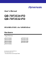
QB-70F3534-PD
QB-70F3532-PD
IECUBE2-POD’s for V850E2/Dx4
Hardware
Target Devices
µPD70F3522
µPD70F3523
µPD70F3524
µPD70F3525
µPD70F3526
Document No. R20UT0270ED0100
Date Published April 2010
Renesas Electronics Europe GmbH
µPD70F3532
µPD70F3535
µPD70F3536
µPD70F3537
To our customers,
Old Company Name in Catalogs and Other Documents
On April 1st, 2010, NEC Electronics Corporation merged with Renesas Technology
Corporation, and Renesas Electronics Corporation took over all the business of both
companies. Therefore, although the old company name remains in this document, it is a
valid Renesas Electronics document. We appreciate your understanding.
Renesas Electronics website: http://www.renesas.com
April 1st, 2010
Renesas Electronics Corporation
Issued by: Renesas Electronics Corporation (http://www.renesas.com)
Send any inquiries to http://www.renesas.com/inquiry.
User’s Manual R20UT0270ED0100
2
Notice
1.
All information included in this document is current as of the date this document is issued. Such information, however, is subject
to change without any prior notice. Before purchasing or using any Renesas Electronics products listed herein, please confirm the
latest product information with a Renesas Electronics sales office. Also, please pay regular and careful attention to additional and
different information to be disclosed by Renesas Electronics such as that disclosed through our website.
2.
Renesas Electronics does not assume any liability for infringement of patents, copyrights, or other intellectual property rights of
third parties by or arising from the use of Renesas Electronics products or technical information described in this document. No
license, express, implied or otherwise, is granted hereby under any patents, copyrights or other intellectual property rights of
Renesas Electronics or others.
3.
You should not alter, modify, copy, or otherwise misappropriate any Renesas Electronics product, whether in whole or in part.
4.
Descriptions of circuits, software and other related information in this document are provided only to illustrate the operation of
semiconductor products and application examples. You are fully responsible for the incorporation of these circuits, software, and
information in the design of your equipment. Renesas Electronics assumes no responsibility for any losses incurred by you or
third parties arising from the use of these circuits, software, or information.
5.
When exporting the products or technology described in this document, you should comply with the applicable export control laws
and regulations and follow the procedures required by such laws and regulations. You should not use Renesas Electronics
products or the technology described in this document for any purpose relating to military applications or use by the military,
including but not limited to the development of weapons of mass destruction. Renesas Electronics products and technology may
not be used for or incorporated into any products or systems whose manufacture, use, or sale is prohibited under any applicable
domestic or foreign laws or regulations.
6.
Renesas Electronics has used reasonable care in preparing the information included in this document, but Renesas Electronics
does not warrant that such information is error free. Renesas Electronics assumes no liability whatsoever for any damages
incurred by you resulting from errors in or omissions from the information included herein.
7.
Renesas Electronics products are classified according to the following three quality grades: “Standard”, “High Quality”, and
“Specific”. The recommended applications for each Renesas Electronics product depends on the product’s quality grade, as
indicated below. You must check the quality grade of each Renesas Electronics product before using it in a particular application.
You may not use any Renesas Electronics product for any application categorized as “Specific” without the prior written consent
of Renesas Electronics. Further, you may not use any Renesas Electronics product for any application for which it is not intended
without the prior written consent of Renesas Electronics. Renesas Electronics shall not be in any way liable for any damages or
losses incurred by you or third parties arising from the use of any Renesas Electronics product for an application categorized as
“Specific” or for which the product is not intended where you have failed to obtain the prior written consent of Renesas Electronics.
The quality grade of each Renesas Electronics product is “Standard” unless otherwise expressly specified in a Renesas
Electronics data sheets or data books, etc.
“Standard”:
Computers; office equipment; communications equipment; test and measurement equipment; audio and visual
equipment; home electronic appliances; machine tools; personal electronic equipment; and industrial robots.
“High Quality”:
Transportation equipment (automobiles, trains, ships, etc.); traffic control systems; anti-disaster systems; anticrime systems; safety equipment; and medical equipment not specifically designed for life support.
“Specific”:
Aircraft; aerospace equipment; submersible repeaters; nuclear reactor control systems; medical equipment or
systems for life support (e.g. artificial life support devices or systems), surgical implantations, or healthcare
intervention (e.g. excision, etc.), and any other applications or purposes that pose a direct threat to human life.
8.
You should use the Renesas Electronics products described in this document within the range specified by Renesas Electronics,
especially with respect to the maximum rating, operating supply voltage range, movement power voltage range, heat radiation
characteristics, installation and other product characteristics. Renesas Electronics shall have no liability for malfunctions or
damages arising out of the use of Renesas Electronics products beyond such specified ranges.
9.
Although Renesas Electronics endeavors to improve the quality and reliability of its products, semiconductor products have
specific characteristics such as the occurrence of failure at a certain rate and malfunctions under certain use conditions. Further,
Renesas Electronics products are not subject to radiation resistance design. Please be sure to implement safety measures to
guard them against the possibility of physical injury, and injury or damage caused by fire in the event of the failure of a Renesas
Electronics product, such as safety design for hardware and software including but not limited to redundancy, fire control and
malfunction prevention, appropriate treatment for aging degradation or any other appropriate measures. Because the evaluation
of microcomputer software alone is very difficult, please evaluate the safety of the final products or system manufactured by you.
10.
Please contact a Renesas Electronics sales office for details as to environmental matters such as the environmental compatibility
of each Renesas Electronics product. Please use Renesas Electronics products in compliance with all applicable laws and
regulations that regulate the inclusion or use of controlled substances, including without limitation, the EU RoHS Directive.
Renesas Electronics assumes no liability for damages or losses occurring as a result of your noncompliance with applicable laws
and regulations.
11.
This document may not be reproduced or duplicated, in any form, in whole or in part, without prior written consent of Renesas
Electronics.
12.
Please contact a Renesas Electronics sales office if you have any questions regarding the information contained in this document
or Renesas Electronics products, or if you have any other inquiries.
(Note 1)
“Renesas Electronics” as used in this document means Renesas Electronics Corporation and also includes its majorityowned subsidiaries.
(Note 2)
“Renesas Electronics product(s)” means any product developed or manufactured by or for Renesas Electronics.
User’s Manual R20UT0270ED0100
3
Regional Information
Some information contained in this document may vary from country to country. Before using any RENESAS product in your application,
please contact the RENESAS office in your country to obtain a list of authorized representatives and distributors. They will verify:
Device availability
Ordering information
Product release schedule
Availability of related technical literature
Development environment specifications (for example, specifications forthird-party tools and components, host computers,
power plugs, AC supply voltages, and so forth)
Network requirements
In addition, trademarks, registered trademarks, export restrictions, and other legal
issues may also vary from country to country.
Renesas Electronics website: http://www.renesas.com
User’s Manual R20UT0270ED0100
4
Warning & Caution
This equipment complies with the EMC protection requirements
WARNING
This is a ‘Class A’ (EN 55022: 2006 + A1:2007) equipment. This equipment can
cause radio frequency noise when used in the residential area. In such cases, the
user/operator of the equipment may be required to take appropriate
countermeasures under his responsibility.
EEDT-ST-001-20
CAUTION
This equipment should be handled like a CMOS semiconductor device. The user
must take all precautions to avoid build-up of static electricity while working with
this equipment. All test and measurement tool including the workbench must be
grounded. The user/operator must be grounded using the wrist strap. The
connectors and/or device pins should not be touched with bare hands.
EEDT-ST-004-10
For customers in the European Union only
Redemption of Waste Electrical and Electronic Equipment
(WEEE) in accordance with legal regulations applicable in the
European Union only: This equipment (including all accessories)
is not intended for household use. After use the equipment
cannot be disposed of as household waste. Renesas Electronics
Europe GmbH offers to take back the equipment. All you need to
do is register at
http://www.renesas.eu/weee.
User’s Manual R20UT0270ED0100
5
Notes for CMOS Devices
1. VOLTAGE APPLICATION WAVEFORM AT INPUT PIN
Waveform distortion due to input noise or a reflected wave may cause
malfunction. If the input of the CMOS device stays in the area between
VIL (MAX) and VIH (MIN) due to noise, etc., the device may
malfunction. Take care to prevent chattering noise from entering the
device when the input level is fixed, and also in the transition period
when the input level passes through the area between VIL (MAX) and
VIH (MIN).
2. HANDLING OF UNUSED INPUT PINS
Unconnected CMOS device inputs can be cause of malfunction. If an
input pin is unconnected, it is possible that an internal input level may
be generated due to noise, etc., causing malfunction. CMOS devices
behave differently than Bipolar or NMOS devices. Input levels of
CMOS devices must be fixed high or low by using pull-up or pull-down
circuitry. Each unused pin should be connected to VDD or GND via a
resistor if there is a possibility that it will be an output pin. All handling
related to unused pins must be judged separately for each device and
according to related specifications governing the device.
3. PRECAUTION AGAINST ESD
A strong electric field, when exposed to a MOS device, can cause
destruction of the gate oxide and ultimately degrade the device
operation. Steps must be taken to stop generation of static electricity
as much as possible, and quickly dissipate it when it has occurred.
Environmental control must be adequate. When it is dry, a humidifier
should be used. It is recommended to avoid using insulators that
easily build up static electricity. Semiconductor devices must be
stored and transported in an anti-static container, static shielding bag
or conductive material. All test and measurement tools including work
benches and floors should be grounded. The operator should be
grounded using a wrist strap. Semiconductor devices must not be
touched with bare hands. Similar precautions need to be taken for PW
boards with mounted semiconductor devices.
4. STATUS BEFORE INITIALIZATION
Power-on does not necessarily define the initial status of a MOS
device. Immediately after the power source is turned ON, devices with
reset functions have not yet been initialized. Hence, power-on does
not guarantee output pin levels, I/O settings or contents of registers.
A device is not initialized until the reset signal is received. A reset
operation must be executed immediately after power-on for devices
with reset functions.
5. POWER ON/OFF SEQUENCE
In the case of a device that uses different power supplies for the
internal operation and external interface, as a rule, switch on the
external power supply after switching on the internal power supply.
When switching the power supply off, as a rule, switch off the external
power supply and then the internal power supply. Use of the reverse
power on/off sequences may result in the application of an
overvoltage to the internal elements of the device, causing
malfunction and degradation of internal elements due to the passage
of an abnormal current. The correct power on/off sequence must be
judged separately for each device and according to related
specifications governing the device.
6. INPUT OF SIGNAL DURING POWER OFF STATE
Do not input signals or an I/O pull-up power supply while the device
is not powered. The current injection that results from input of such a
signal or I/O pull-up power supply may cause malfunction and the
abnormal current that passes in the device at this time may cause
degradation of internal elements. Input of signals during the power off
state must be judged separately for each device and according to
related specifications governing the device.
User’s Manual R20UT0270ED0100
6
Introduction
Readers
This manual is intended for users who wish to perform debugging using the
IECUBE2-POD’s.The readers of this manual are assumed to be familiar with the
device functions and usage, and to have knowledge of debuggers.
Purpose
This manual is intended to give users an understanding of the basic specifications
and correct usage of the IECUBE2-POD’s.
Organization
This manual is divided into the following sections.
How to Read This Manual
General
Setup procedure
Settings at product shipment
Notes
Optional functions
It is assumed that the readers of this manual have general knowledge in the fields
of electrical engineering, logic circuits, and microcontrollers.
This manual describes the basic setup procedures and how to set switches to
understand the overall functions and usages of the IECUBE2-POD’s.
Read this manual in the order of the CONTENTS.
To know the manipulations, command functions, and other software-related settings
of the IECUBE2-POD’s.
See the user’s manual of the debugger (supplied with the IECUBE2-POD’s) to be
used.
Conventions
Note:
Caution:
Remark:
Numeric representation:
Footnote for item marked with Note in the text
Information requiring particular attention
Supplementary information
Binary ... xxxx or xxxxB
Decimal ... xxxx
Hexadecimal ... xxxxH
Prefix indicating power of 2 (address space, memory capacity):
K (kilo): 210 = 1,024
M (mega): 220 = 1,0242
Terminology
The meanings of the terms used in this manual are described in the table below.
Term
Meaning
Target device
Target system
This is the device to be emulated.
This is the system to be debugged (system provided
by the user).
This includes the target program and the hardware
provided by the user.
Generic name for Renesas Electronics highperformance, compact in-circuit emulator.
This is IECUBE2 peripheral to interface with the
target system.
IECUBE2TM
POD
User’s Manual R20UT0270ED0100
7
Related Documents
Please use the following documents in combination with this manual.
The related documents listed below may include preliminary versions. However,
preliminary versions are not marked as such.
Documents Related to Development Tools (User’s Manuals)
Document Name
User’s Manual IECUBE2-POD for V850E2/Dx4
User’s Manual(Preliminary)IECUBE2 main (QB-V850E2) InCircuit Emulator
Caution
Trademarks
Document Number
This manual
ZUD-CD-10-0092
(actual)
The related documents listed above are subject to change
without notice. Be sure to use the latest version of each
document for designing, etc.
Green Hills, the Green Hills logo, CodeBalance, GMART, GSTART, INTEGRITY,
and MULTI are registered trademarks of Green Hills Software, Inc. AdaMULTI,
EventAnalyzer, G-Cover, GHnet, GHnetLite, Green Hills Probe, Integrate, ISIM,
PathAnalyzer, Quick Start, ResourceAnalyzer, Safety Critical Products, Slingshot,
SuperTrace Probe, TimeMachine, and TotalDeveloper are trademarks of Green Hills
Software, Inc.
Windows and Windows Vista are either registered trademarks or trademarks of
Microsoft Corporation in the United States and/or other countries.
PC/AT is a trademark of International Business Machines Corporation.
All other company, product, or service names mentioned in this documentation may
be trademarks or service marks of their respective owners.
User’s Manual R20UT0270ED0100
8
Guarantee & Safety precautions
1. Circumstances not covered by product guarantee
If the product was disassembled, altered, or repaired by the customer.
If it was dropped, broken, or given another strong shock.
Use at overvoltage, use outside guaranteed temperature range, storing outside guaranteed
temperature range.
If power was turned on while the AC adapter, interface cable, or connection to the target system was
in an unsatisfactory state.
If the cable of the AC adapter, the interface cable, the target cable, or the like was bent or pulled
excessively.
If an AC adapter other than the supplied product was used.
If the product got wet.
If the product and target system were connected while a potential difference existed between the
GND of the product and the GND of the target system.
If a connector or cable was connected or disconnected while power was being supplied to the
product.
If an excessive load was applied to a connector or cable.
If the product is used or stored in an environment where an electrostatic or electrical noise is likely to
occur.
2. Safety precautions
If used for a long time, the product may become hot (50 to 60°C). Be careful of high temperature
burns and other dangers due to the product becoming hot.
Be careful of electrical shock. There is a danger of electrical shock if the product is used as
described above in 1.1 Circumstances not covered by product guarantee.
The AC adapter supplied with the product is exclusively for this product, so do not use it with other
products.
User’s Manual R20UT0270ED0100
9
Table of Contents
Introduction ..................................................................................................................................... 7
List of Figures ............................................................................................................................... 11
List of Tables ................................................................................................................................. 11
1.
General.................................................................................................................................... 12
1.1
1.2
1.3
1.4
Hardware Specifications ..................................................................................................................... 12
System Specification ........................................................................................................................... 13
Adapters, Connectors.......................................................................................................................... 14
Package Contents ................................................................................................................................ 15
2.
Setup Procedure .................................................................................................................... 16
2.1
2.2
2.3
2.4
2.5
Installation of Software tools .............................................................................................................. 16
Clock Settings ...................................................................................................................................... 16
Connection of System ......................................................................................................................... 17
Start the Software Tool ........................................................................................................................ 18
Shut down procedure .......................................................................................................................... 19
3.
Differences between Target Device and POD ..................................................................... 20
3.1 Electrical differences ........................................................................................................................... 20
3.1.1 Electrical differences on power pins ................................................................................................... 20
3.1.2 Target power on .................................................................................................................................. 20
3.1.3 Electrical differences on port pins ....................................................................................................... 21
3.2 Functions not emulated by real-chip on the POD............................................................................. 21
3.2.1 RAM contents during deep-stop ......................................................................................................... 21
3.2.2 RESET function ................................................................................................................................... 21
3.2.3 POC function ....................................................................................................................................... 21
3.2.4 WAKE, PWGD function ....................................................................................................................... 22
3.2.5 Target Memory emulation concept (QB-70F3532-PD only) ............................................................... 23
3.3 Cautions ................................................................................................................................................ 25
3.3.1 Data flash read access........................................................................................................................ 25
3.3.2 Data flash read access........................................................................................................................ 25
3.3.3 Reset issued by the debugger ............................................................................................................ 25
3.3.4 Reset during break mode .................................................................................................................... 25
3.3.5 Flash .................................................................................................................................................... 25
3.3.6 FLMD0 during TRESETZ active.......................................................................................................... 25
3.3.7 AHB time out during memview ............................................................................................................ 25
3.3.8 Single stepping entry of standby modes ............................................................................................. 26
3.3.9 Not supported functions ...................................................................................................................... 27
User’s Manual R20UT0270ED0100
10
List of Figures
Figure 1-1: Description of IECUBE2 POD ...................................................................................................12
Figure 1-2 Description of Target Connection Details ..................................................................................14
Figure 1-3 Target Connection Details (Height) ...........................................................................................14
Figure 2-1 Clock setup ................................................................................................................................16
Figure 2-2 System setup .............................................................................................................................17
Figure 2-3 Turn on system ..........................................................................................................................18
List of Tables
Table 1-1 Target devices subject of emulation ...........................................................................................12
Table 1-2 Target specifications ...................................................................................................................12
Table 3-1 Memory interface pins (on POD) ................................................................................................23
User’s Manual R20UT0270ED0100
11
1. General
Each POD is part of an in-circuit emulator system for emulating the target devices shown below.
Hardware and software can be debugged efficiently in the development of systems in which the target device is
used. This manual describes basic setup procedures, hardware specifications, system specifications, and how to set
switches. For the whole system, both User’s Manual’s, this and the IECUBE2 User’s manual are mandatory.
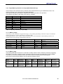
Table 1-1 Target devices subject of emulation
Device
Nick
name
Package
Frequency
µPD70F3522
µPD70F3523
µPD70F3524
µPD70F3525
µPD70F3526
µPD70F3532
µPD70F3535
µPD70F3536
µPD70F3537
DJ4
DJ4
DJ4
DJ4
DJ4
DN4-H
DP4-H
DP4-H
DP4-H
QFP144
QFP144
QFP144
QFP144
QFP144
BGA352
BGA408
BGA408
BGA408
[MHz]
80
80
120
120
120
160
160
160
160
Internal flash
memory
[kB]
256
512
1024
2048
3072
3072
3072
3072
3072
Internal
RAM
[kB]
24
48
96
192
256
128
256
256
256
vRAM
POD
[kB]
vRAM i/f
3072
5120
8192
QB-70F3534-PD
QB-70F3534-PD
QB-70F3534-PD
QB-70F3534-PD
QB-70F3534-PD
QB-70F3532-PD
QB-70F3534-PD
QB-70F3534-PD
QB-70F3534-PD
The QB-70F3532-PD emulates the µPD70F3532 device. For using profiling function on other devices, this
POD could be used (refer to chapter 3 too).
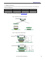
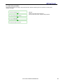
1.1 Hardware Specifications
Table 1-2 Target specifications
Parameter
CVDD,MCVDD
ExVDD,AVDD,OSCVDD,SMVDD,REGxVDD
RVDD,BxVDD,FVDD,DVDD
Maximum operating frequency
Capability of main clock oscillator
2x Ring internal oscillator
Sub external oscillator
Main external oscillator
Operating temperature range
Storage temperature range
External dimensions
Power Consumption
Supplied by IECUBE2
Supply from target system
Weight
Host Interface
Target system
Interface Voltage
Specifications
1.1 to 1.3V
2.7 to 5.5V
3.0 or 3.6V
160 MHz
4 to 20MHz
8MHz & 240kHz (typ.)
32kHz (typ.)
4MHz (typ.)
-0 to 40°C (No condensation)
-15 to 60°C (No condensation)
55 mm x 55 mm
(part of the IECUBE2 power consumption)
(approx. device power consumption or less)
Approx. 40g
Control i/f to IECUBE2
Figure 1-1: Description of IECUBE2 POD
User’s Manual R20UT0270ED0100
12
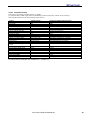
1.2 System Specification
This section shows the QB-70F3534-PD / QB-70F3532-PD system specifications. For the usage of the debugging
function, refer to the documentation of the debugger.
Emulation memory
capacity
Program execution
functions
Event functions
Parameter
Internal FLASH
Internal RAM
Internal Video RAM
External memory
Real-time execution function
Non-real-time execution function
Detection of execution
Trace functions
Detection of access
Pass counter
Sequential
Modification when running
Hardware break
Software break
Other
Trace data types
Time measurement
functions
Trace events
Memory capacity
Other
Measurement clock
Measurement objects
Break functions
Maximum measurement time
Minimum resolution
Measurement results
Other
Other functions
Specification
3 MB
256KB
8 MB / None *
None / vRAM i/f *
Available
Available
(Step execution in source level depends on debugger)
Pre-execution: 4 points (only for break function)
Post-execution: 8 points
6 points
12 bits
4 steps
Available
4 Available
96 Available
Trace full break, forced break, timer overflow break
Branch-source PC, branch-destination PC, access data,
access
address, R/W status, time stamp, DMA access data,
DMA access
address, DMA R/W status, DMA transfer count, DMA
channel number
Delay trigger, section, qualify
512K frames
Trace full stop
200 MHz
Beginning through end of program execution
Start event through end event (6 sections)
Approximately 195 hours (When using measurementdedicated clock
divided by 32)
5 ns
Execution time (Start through end of execution)
Maximum, minimum, average, pass count (between
events)
Timer overflow break function (1 point)
Open break function, peripheral break function, mask
function(_RESET, internal reset)
Note: *(QB-70F3534-PD / QB-70F3532-PD)
User’s Manual R20UT0270ED0100
13
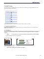
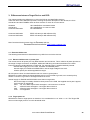
1.3 Adapters, Connectors
The following adapters and connectors are necessary to connect the POD to the target system. These adapters and
sockets are sold separately.
Type
Exchange adapter
Emulator connector
Target connector
QFP package
QB-144GJ-EA-60T
QB-144GJ-YQ-01T
QB-144GJ-NQ-01T
BGA package
QB-408F1-EA-61T
BSSOCKET408
BGA package
QB-352F1-EA-60T
QB-352F1-NQ-01T
Note: Products of Tokyo Eletech Corporation (http://www.tetc.co.jp)
Figure 1-2 Description of Target Connection Details
Figure 1-3 Target Connection Details (Height)
User’s Manual R20UT0270ED0100
14
1.4 Package Contents
The packaged items might vary depending on the region in which the product is purchased. Therefore, confirm that the
items in the attached packing list are included.
Refer to the actual Package Contents List (PCL) for the Products supplied with the IECUBE2 POD’s.
User’s Manual R20UT0270ED0100
15
2. Setup Procedure
This chapter explains the IECUBE2 setup procedure. Setup can be completed by performing installation/setup in the
order in which it appears in this chapter.
Remark: Observe the power up sequence. Do not power on target, if POD is not powered.
2.1 Installation of Software tools
Before setting up hardware, install the necessary software tools. For details about how to do so, see the documents
supplied with the software tools.
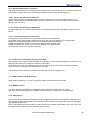
2.2 Clock Settings
The main clock is generated by the oscillator in the emulation POD. In case using the default frequency of the crystal, the
setting is not required to be changed. In case of customer specific frequency modification is necessary, see following
procedures.
Caution
This product does not support clock input from target. Sublock is fixed to 32.768kHz.
(1) Open the emulation POD cover as shown below.
Figure 2-1 Clock setup
(2) Mount the resonator and capacitors onto the parts board in the emulation POD.
(3) Close the emulation POD cover.
Factory setting: 4MHz crystal is mounted upon shipment
User’s Manual R20UT0270ED0100
16
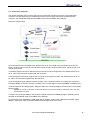
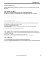
2.3 Connection of System
This section describes how to mount and connect components including connectors. Mount the target
connector onto the target board. For details about how to do so, see the document supplied with the
connector. For details and setup about IECUBE2 refer to the IECUBE2 User’s Manual.
Figure 2-2 System setup
0) Connecting POD and IECUBE2 main. Remove top cover of the POD using a screw driver for the four
screws. Plug the cable connector onto the POD connector CN1. Observe the direction. Mount the top cover
with the four screws.
1) Soldering Target Connector: Mount the target connector onto the target board. For details about how to
do so, refer to the document supplied with the connector.
2) Connecting ICE Connector: Plug the ICE connector to the target connector. For details about how to do
so, refer to the document supplied with the connector.
3) Connecting Exchange Adapter: Note the position of pin 1 (positioned at the cut corner) and connect the
exchange adapter to the ICE connector (144QFP only) or to the target connector (408BGA or 352BGA only).
4) Connecting POD and target system: Plug the POD to the exchange adapter. Be careful not to excessively
bend the cable.
Caution: Do not put any pressure on the small devices on the POD (on PCB top and bottom side). They may
be damaged in that case.
To remove the exchange adapter, use the stick included within the IECUBE2 package to gradually pull up
the sides of the adapter (refer to IECUBE2 User’s Manual).
5) Connecting to the IECUBE2 the USB cable and AC adapter: Connect the USB cable and power supply
adapter. At this time, make sure that IECUBE2 and the target system are not on.
User’s Manual R20UT0270ED0100
17
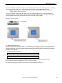
6) Turn on IECUBE2: At this time, make sure that the target system is not on. When the power is turned on,
the System and POD LED turn on. If these LEDs blink or remain off, IECUBE2 might be faulty.
Remark: When the power is turned on for the first time, Plug and Play starts and sets up the USB driver.
Continue setup according to the wizard.
7) Turn on the target system: After the power is on, the TARGET LED turns on. If the LED remains off,
connectors might be connected poorly, the emulation POD cable might be broken, or voltage might not be
correctly applied to the power supply pins of the micro-controller (such as VDD).
Figure 2-3 Turn on system
2.4 Start the Software Tool
After the above procedure, the system starts up. For downloading and debugging a program by using the GHS MULTI
generic debugger, please make sure that you have establish a USB connection between the host and the IECUBE2
emulation environment. For doing so, please specify the following command string within the first line of your debugger
script file (*.rc file). Example:
Stand-alone mode (without connected target):
connect 850eserv2 -iecube -e2 -ip=C:\GHS\v850e -df=dfxxxx.800 -id ffffffffffffffffffffffff
Target mode (with connected target):
connect 850eserv2 -iecube -e2 -ip=C:\GHS\v850e -df=dfxxxx.800 -tc -id ffffffffffffffffffffffff
Please note, when -df, -ip and environment variable DEVICE_FILE, IEPATH are specified simultaneously,
the device file and the directory specified by -df and -ip are given to priority.
For details about debugging procedures, see the document supplied with the software tool.
User’s Manual R20UT0270ED0100
18
2.5 Shut down procedure
Shut down the system according to the procedure below. Note that shutting down the system incorrectly might
damage IECUBE2.
Remark:
Observe the power down sequence.
Do not power down POD, if target is still powered.
User’s Manual R20UT0270ED0100
19
3. Differences between Target Device and POD
This chapter explains the differences on using the POD to the V850E2/Dx4 devices.
There are other User’s Manuals important, covering the specific description of the devices, the Core
Architecture and the IECUBE2. Refer to these versions or check for current version:
Hardware
Architecture
Customer Notification
UM -V850E2/Dx4 U20018EE0V3UM00
UM -V850E2/Dx4 U17135EJ1V1UM00
CN -V850E2/Dx4
Customer Notification
Customer Notification
EEDT-OP-0044 (for QB-70F3534-PD)
EEDT-OP-0046 (for QB-70F3532-PD)
Note: Download the documents from the Renesas web site.
Renesas Electronics website: http://www.renesas.com
3.1 Electrical differences
The following listed electrical characteristics may differ from tool to the devices.
3.1.1 Electrical differences on power pins
The current load on all power pins may differ between tool and device. This is valid for all power pins due to
the usage of target connectors, ea-adapter, additional PCB wiring and internal switches on the POD.
Power groups are handled different on POD side. For example power is supplied statically internal.
Internal static supply for Core, Flash, Oscillator and eDRAM power.
Internal supply for E0VDD and REGCVDD in case of target voltage is less 3.0V.
All other power pins will be supplied from target.
All VSS-pins are short circuited inside the tool to a common ground plane.
REG0VSS is used to detect the target-hardware and is not connected to ground, but to a weak pull-up
resistor. Connect it to ground on the target hardware as usual.
Internal supply for E0VDD and REGCVDD is less than on target side.
Due to the usage of schottky diodes for these power on the POD, the supplied device part is approx.
0.2V less than on target side.
Ports - P0, JP0, Wake output levels are approx. 0.2V lower than on device
LVI
- effective levels are approx. 0.2V higher than on device
POC - effective levels are approx. 0.2V higher than on device
VLVF - not supported
3.1.2 Target power on
REG0VDD is used for target power on detection. It is considered to be “on” when > 2.7V. The Target LED
turns on when target power is over this threshold value.
User’s Manual R20UT0270ED0100
20
3.1.3 Electrical differences on port pins
The electrical characteristics of the port pins may differ between tool and device. This is valid for all pins due
to the usage of target connectors, ea-adapter and additional PCB wiring for each signal pin.
3.1.3.1 Electrical differences on ADC pins
As any of the analogue input signals and the reference voltage is connected via target connectors, eaadapter, additional PCB wiring and internal switches on the POD for Vref, the converted values may differ
between tool and device.
3.1.3.2 Electrical differences on RSDS pins
As these signals are not routed as different pairs on the POD-PCB, the signal may differ between tool and
device.
3.1.3.3 Electrical differences on other pins
IC/FLMD0 has a 12k1 pull-down and may have different input characteristics.
P0.1/FLMD1 has a 100k pull-down (QB-70F3532 only) and may have different input characteristics.
RESETZ is emulated with similar circuit may have different input characteristics.
PWGD is emulated with similar circuit may have different input characteristics.
WAKE is emulated with similar circuit may have different input characteristics.
X1,X2 and XT1,XT2 are not connected to target.
3.2 Functions not emulated by real-chip on the POD
The emulation tool is based on real-chip base. All notifications of the real device applies for the POD too. For
this information refer to the customer notification of the device.
For functions which are not emulated by the real-chip on the POD, discrete circuits are used to emulate
these functions. For these functions the behavior may differ.
The following listed functions are emulated may differ from tool to the target devices.
3.2.1 RAM contents during deep-stop
When entering deep-stop, 1.2V are not removed. RAM content will remain unchanged.
3.2.2 RESET function
The Reset signal is emulated with an additional circuit. The input is sampled in every 200ns.
After that, true RUN will happen but IECUBE2 needs hundreds of ms delay than on target device.
3.2.3 POC function
POC function is emulated with an additional circuit. The period of POC (Power On Clear) is longer than on a
target device, because the emulation chip is also reset. The emulator reconfigures the setting for debugging
(e.g. breakpoint) after POC.
Parts of trace data before POC (Power On Clear) may be lost, because the emulation chip is also reset. The
trace data FIFO in emulation chip is cleared in case of a POC.
User’s Manual R20UT0270ED0100
21
3.2.4 WAKE, PWGD function
Wake and PWGD function is emulated with an additional circuit. The generation time may differ than on the
target device.
3.2.4.1 Watchdog timer (WDTA)
During break mode the WDTA is always stopped, even if peripheral break is disabled.
The WDT macro clears WDTA-counter to 0x0000 when you write RUN (WDTE = 0xAC) during break.
3.2.4.2 Reset Controller (RESF)
The RESF SFR is cleared by software reset and on initial startup, as well as by a target reset.
3.2.4.3 Clock Monitor (CLMA)
The CLMA can be triggered in two different ways:
a) The CLMA can be triggered by removing the target clock X1. This can be done by removing the clock
board under the plastic lid of the emulator. However it is strongly suggest not to remove the clock board for
this feature. We recommend using solution b) instead.
b) The CLMA can be triggered by SFR write.
If the CLMA is triggered (i.e. the main clock fails) during break, the reset will be generated just after
restarting from break.
The CLM will continue to operate in peripheral break mode.
3.2.4.4 Peripheral macros will operate during peripheral break when retry registers are accessed
The peripheral clock will run for a few cycles when peripheral break is enabled and an SFR requiring RETRY
is accessed in break mode.
Because of this, all peripheral macros will operate for these few cycles.
An access to a SFR can occur by the SFR window, a watch window or the TCL console.
3.2.4.5 iRAM content
The content of the iRAM will be unchanged after a RESET/Target Power off/on.
This behavior may differ than on the target device. In the target device the contents of the iRAM may change
to that contents before a RESET/Power off/on.
User’s Manual R20UT0270ED0100
22
3.2.5 Target Memory emulation concept (QB-70F3532-PD only)
The emulation of the external memory interface (device uPD70F3532 only) is substituted on POD. This
memory interface is not connected to the target application.
The memory interface to the target is clamped at an inactive level with a 10k pull down.
The software may differ for the setup of the memory controller.
Port
P21[6]
P21[13]
P21[8]
P21[14]
P21[15]
P22[0]
P22[6:3]
P22[2:1]
P26[12:0]
P23[15:0]
P24[15:0]
SDRAM signal
CK
CKE
CSZ
RASZ
CASZ
WEZ
DQM[3:0]
BA[1:0]
A[12:0]
DQ[31:16]
DQ[15:0]
Termination
33 Ohm series damping
10k pull-down
10k pull-up
10k pull-up
10k pull-up
10k pull-up
10k pull-down
10k pull-down
10k pull-down
10k pull-down
10k pull-down
Table 3-1 Memory interface pins (on POD)
3.2.5.1 Memory usage
The memory can be used either for application usage, or for profiling, depending on the device subject of emulation
and the requirements. It can be used both for code and for data.
The profiling memory can be used by software profiling tools to store information collected during run-time. No
hardware support for profiling is implemented in this tool.
Device(s)
Family
Package
uPD70F3522/23
uPD70F3524/25/26
uPD70F3535
uPD70F3536
uPD70F3537
uPD70F3532
DJ4
DJ4
DP4-H
DP4-H
DP4-H
DN4-H
LQFP/HQFP144
LQFP/HQFP144
BGA408
BGA408
BGA408
BGA352
(e)DRAM
(substitute)
None
None
3MB
5MB
8MB
0..64MB
Max. available profiling memory
(optional)
64MB/32MB
64MB/32MB
61MB/23MB
59MB/32MB
56MB/32MB
64MB reduced by the amount of target
memory
3.2.5.2 Memory map
The profiling RAM will be located in an area that is usually used for HSFI1 interface (for devices supporting
this feature). The HSFI1 interface usually is located in the area from 0xF400 0000-0xF77F FFFF (56MB).
To be able to access the profiling memory this area is reduced according to the following table.
DJ4 devices remain all their features; they just gain the profiling memory.
Mode
DP4-H
HSFI1
size
56MB
DN4-H
0MB
DP4-H profiling
32MB
HSFI1 area
0xF400 00000xF77F FFFF
0xF400 00000xF5FF FFFF
DRAM
type
Internal
eDRAM
External
SDRAM
Emulation
only
DRAM
size
8MB
0..64MB
8MB
DRAM area
0xF780 00000xF7FF FFFF
0xF400 00000xF7FF FFFF
0xF780 00000xF7FF FFFF
User’s Manual R20UT0270ED0100
Profiling
mem. size
0MB
Profiling
mem. area
-
0..64MB
0xF400 00000xF7FF FFFF
0xF600 00000xF7FF FFFF
32MB
23
3.2.5.3 Available memory
The amount of (external) available memory is 64MB.
It is implemented as SDR (single data rate) SDRAM (synchronous dynamic random access memory).
The selected RAM device has the following characteristics:
Feature
Interface
Size [bytes]
JEDEC SDR SDRAM compliant
Bus width [bits]
Bank address width [bits]
Row address width [bits]
Column address width [bits]
Max. frequency (tck) [MHz]
Suitable for SSCG
Auto refresh
Auto refresh cycle timing (tREF)
Refresh cycle timing (tREF)
Self refresh
Precharge all
Auto precharge
Refresh command timing (tRC)
[CLKs]
CAS latency (tRCD) [CLKs]
Activate timing (tRCD) [CLKs]
Command period (tRP) [CLKs]
Burst (4) allowed
Burst abort
Mode setting pattern
Mode timing (tMRD)
DQM during read
eDRAM (LEHUA)
3.3V
8M
No
32bit
2 (=4 banks)
13
6
126 (120 + 5% dithering)
Yes
Yes
4096/2ms
2ms (4096 cycles)
No
No (at init only)
Yes (during read and write)
2
Substitution RAM (IS42S32160A-75BL)
Same
64MB
Yes
Same
Same
Same
9 (A10 is auto-precharge)
Same (133MHz is supported, but not required)
Same
Same
Same (8192/64ms), more often is no problem)
Same (64ms, more often is no problem)
Same (supported, but not required)
Same (supported, but not required)
Same
9 (70ns)
3
2(2/4)
2
Yes (sequential address only)
No
(see SDM for pattern)
Same (and 2)
3 (20ns)
3 (20ns)
Same (interleaved also supported, but not required)
Same (supported, but not required)
Same (more features supported, but not required)
2CLKs
Same (supported, but not required)
Not supported
For setup refer to Hardware UM -V850E2/Dx4 – (chapter 37)
User’s Manual R20UT0270ED0100
24
3.3 Cautions
3.3.1 Data flash read access
The data flash read access is only 32 bit (GHS memview)
3.3.2 Data flash read access
The iRAM ECC error occurs, when accessing unused areas. This is same behavior as on device.
In case of power down iRAM content will not be deleted and ECC error will not occur; may be different from
device.
3.3.3 Reset issued by the debugger
A reset issued by the debugger (e.g. "target rst") will behave the same way as power-cycling the device. I.e.
the status SFRs RESF and SRESF will be cleared.
3.3.4 Reset during break mode
A reset applied to the target RESETZ pin will not be handled if the debugger is in break mode. The reset will
be lost unless it is held active until the application starts to run again.
3.3.5 Flash
The flash lifetime for data and code flash on the POD, as it is real chip based, is the same as on device.
The User program is downloaded to the flash memory of the device mounted on POD. However, it is
recommended to download the application program at the beginning of a debug session in order to
guarantee proper operation.
In case of repair of a POD, the Flash contents will be cleared during repair.
3.3.6 FLMD0 during TRESETZ active
If target TFLMD0 is clamped to High level during TRESETZ, the POD will not be functionable.
3.3.7 AHB time out during memview
The AHB time out is set to unlimited (because of GFX issue, ETAWRL = 0x0000)
If you debug the below sequence and have a memory window (memview GHS) with eDRAM contents open,
the debugger will loose connection as soon as you set the memory controller into idle state.
User’s Manual R20UT0270ED0100
25
do
{
PROTCMD5 = 0x000000A5;
// write A5 fixed value to protection command register
GSSDICTRL = 0x00000001;
// write desired value to destination
GSSDICTRL = 0xFFFFFFFE;
// write bit-wise inversion to destination
// make sure to close the debugger memory window here
GSSDICTRL = 0x00000001;
// write desired value to destination
} while ( _PROTS5ERR == 1 );
// check error state
while ( GSSDICTRL != 3 );
// wait for idle request acknowledge
3.3.8 Single stepping entry of standby modes
Summary:
Debugger might loose connection and in most cases it is able to resume operation after system wake up.
Furthermore, by temporary (i.e. in a debugger data window) masking the (normally unmasked) debugger
wake up flag it is possible to debug the deep stop sequence. Set the debugger connection timeout to be long
enough for another wake up event to occur.
Additional Info:
The connection loss is not influenced by any data or memory window.
Disabling debugger wake up for ISO1only does not prevent the connection loss issue and still and does not
solve the debugging of the deep stop sequence for ISO0. And additionally, after debugger wake up the
system is not really operational, as the ISO1 is still disabled.
Details:
Case 1: WUFH0 bit cleared, WUFH1 bit set (wake up by debugger enabled only for ISO0)
a) Stepping through deep stop entry sequence:
- For ISO1: no problem
- For ISO0: - as expected immediate wake up after DS entry (in the debugger window you see the
status: HARDWARE STOP, but in fact there is no DS entry, as the software just continues without
"going through reset")
The debugger does not lose connection independent from any memory or data windows open
b) Stepping over deep stop entry sequence:
The DS mode is reached as expected. Wake up by debugger works for ISO0, ISO1 remains
stopped.
The debugger does not looses connection independent from any memory or data windows open.
Case 2: WUFH0 bit cleared, WUFH1 bit cleared (wake up by debugger enabled for ISO0 and ISO1)
a) Stepping through deep stop entry sequence :
- For ISO1: as expected no standby, so the software remains in a while loop waiting for the ISO1 to
report stand by mode.
- For ISO0: no DS entry attempt - the software waits for ISO1
The debugger does not crash or lose connection independent from any memory or data
windows open
b) Stepping over deep stop entry sequence :
The DS mode is reached as expected.Target: CPU status (0x8): HARDWARE STOP. Wake up by
debugger works for ISO0 and ISO1. The debugger does not crash or looses connection
independent from any memory or data windows open.
Case 3: WUFH0 bit set, WUFH1 bit set (wake up by debugger disabled for ISO0 and ISO1)
a) Stepping through deep stop entry sequence :
- For ISO1: no problem
- For ISO0: after completing the last write command of the protected sequence that sets the ISO into
deep stop the debugger can't set the breakpoint for the next instruction and might loose connection.
It is not influenced by any open data or memory window. The debugger looses connection to the
target and tries to reconnect. After a while (connection timeout period) it shows a dialogue box
asking if you want to continue waiting or terminate the connection. If you choose to continue and
generate a valid wake up event the debugger resumes operation at the expected entry point (reset
User’s Manual R20UT0270ED0100
26
vector). This was a bit different for the umbrella device (as far as I remember ;) There a resume of
operation did not work.
b) Stepping over deep stop entry sequence :
The DS mode is reached as expected. In the debugger command window it shows:
Target: CPU status (0x8): HARDWARE STOP. Wake up by debugger of course does not work for
ISO0 and ISO1. An attempt to set a breakpoint or a click on the debugger stop button leads to
connection loss as described above. If you generate a valid wake up event before the connection
timeout occurs the debugger resumes operation at the expected entry point (reset vector). After the
dialogue box occurrence (connection timeout) the debugger cannot resume after wake up. But it is
still able to reset the target.
Case 4: WUFH0 bit set, WUFH1 bit cleared (wake up by debugger disabled for ISO0 and enabled for ISO1)
This case is not used.
3.3.9 Not supported functions
The following functions are not supported by the POD
OCD
Boundary Scan
FP5 programming
User’s Manual R20UT0270ED0100
27