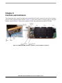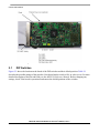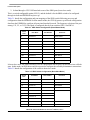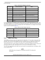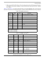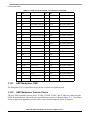
1
MSC8156 Advanced Mezzanine
Card User’s Manual
MSC8156AMCUM
Rev. 0
01/2010
How to Reach Us:
Home Page:
www.freescale.com
Web Support:
http://www.freescale.com/support
USA/Europe or Locations Not Listed:
Freescale Semiconductor, Inc.
Technical Information Center, EL516
2100 East Elliot Road
Tempe, Arizona 85284
+1-800-521-6274 or
+1-480-768-2130
www.freescale.com/support
Europe, Middle East, and Africa:
Freescale Halbleiter Deutschland GmbH
Technical Information Center
Schatzbogen 7
81829 Muenchen, Germany
+44 1296 380 456 (English)
+46 8 52200080 (English)
+49 89 92103 559 (German)
+33 1 69 35 48 48 (French)
www.freescale.com/support
Information in this document is provided solely to enable system and software
implementers to use Freescale Semiconductor products. There are no express or
implied copyright licenses granted hereunder to design or fabricate any integrated
circuits or integrated circuits based on the information in this document.
Freescale Semiconductor reserves the right to make changes without further notice to
any products herein. Freescale Semiconductor makes no warranty, representation or
guarantee regarding the suitability of its products for any particular purpose, nor does
Freescale Semiconductor assume any liability arising out of the application or use of
any product or circuit, and specifically disclaims any and all liability, including without
limitation consequential or incidental damages. “Typical” parameters which may be
provided in Freescale Semiconductor data sheets and/or specifications can and do
vary in different applications and actual performance may vary over time. All operating
parameters, including “Typicals” must be validated for each customer application by
customer’s technical experts. Freescale Semiconductor does not convey any license
under its patent rights nor the rights of others. Freescale Semiconductor products are
not designed, intended, or authorized for use as components in systems intended for
Japan:
Freescale Semiconductor Japan Ltd.
Headquarters
ARCO Tower 15F
1-8-1, Shimo-Meguro, Meguro-ku
Tokyo 153-0064
Japan
0120 191014 or
+81 3 5437 9125
[email protected]
surgical implant into the body, or other applications intended to support or sustain life,
Asia/Pacific:
Freescale Semiconductor China Ltd.
Exchange Building 23F
No. 118 Jianguo Road
Chaoyang District
Beijing 100022
China
+86 010 5879 8000
[email protected]
unintended or unauthorized use, even if such claim alleges that Freescale
For Literature Requests Only:
Freescale Semiconductor
Literature Distribution Center
P.O. Box 5405
Denver, Colorado 80217
+1-800 441-2447 or
+1-303-675-2140
Fax: +1-303-675-2150
LDCForFreescaleSemiconductor
@hibbertgroup.com
Document Number: MSC8156AMCUM
Rev. 0, 01/2010
or for any other application in which the failure of the Freescale Semiconductor product
could create a situation where personal injury or death may occur. Should Buyer
purchase or use Freescale Semiconductor products for any such unintended or
unauthorized application, Buyer shall indemnify and hold Freescale Semiconductor
and its officers, employees, subsidiaries, affiliates, and distributors harmless against all
claims, costs, damages, and expenses, and reasonable attorney fees arising out of,
directly or indirectly, any claim of personal injury or death associated with such
Semiconductor was negligent regarding the design or manufacture of the part.
Freescale, the Freescale logo, and StarCore and the Freescale logo are
trademarks or registered trademarks of Freescale Semiconductor, Inc. in
the U.S. and other countries. All other product or service names are the
property of their respective owners. The Power Architecture and Power.org
word marks and the Power and Power.org logos and related marks are
trademarks and service marks licensed by Power.org. RapidIO is a
registered trademark of the RapidIO Trade Association. ARM is the registered
trademark of ARM Limited. ARMnnn is the trademark of ARM Limited.
© Freescale Semiconductor, Inc., 2010. All rights reserved.
Contents
Paragraph
Number
Title
Page
Number
About This Book
Audience ............................................................................................................................ xi
Organization....................................................................................................................... xi
Suggested Reading............................................................................................................. xi
Related Documentation.................................................................................................. xi
Conventions ...................................................................................................................... xii
Signal Conventions ........................................................................................................... xii
Acronyms and Abbreviations .......................................................................................... xiii
Chapter 1
Overview
1.1
1.2
1.2.1
1.2.2
1.3
1.4
1.5
1.6
1.6.1
1.6.2
1.7
Introduction...................................................................................................................... 1-1
Working Configuration .................................................................................................... 1-2
Standard AMC Mode................................................................................................... 1-2
Stand-Alone Mode....................................................................................................... 1-2
Features ............................................................................................................................ 1-3
External Connectors......................................................................................................... 1-4
Specifications................................................................................................................... 1-5
Hardware Preparation and Installation ............................................................................ 1-6
Unpacking Instructions ................................................................................................ 1-6
Installation Instructions................................................................................................ 1-6
Memory Map ................................................................................................................... 1-7
Chapter 2
Controls and Indicators
2.1
2.2
2.3
DIP Switches.................................................................................................................... 2-2
LEDs ................................................................................................................................ 2-5
Push Buttons .................................................................................................................... 2-5
Chapter 3
Functional Description
3.1
3.2
3.3
3.3.1
JTAG Debug Interface ..................................................................................................... 3-1
DDR3 Memory ................................................................................................................ 3-2
SerDes Configuration ...................................................................................................... 3-3
SRIO Switch Configuration Modes............................................................................. 3-3
MSC8156 Advanced Mezzanine Card User’s Manual, Rev. 0
Freescale Semiconductor
iii
Contents
Paragraph
Number
3.3.2
3.3.3
3.4
3.4.1
3.4.2
3.4.3
3.5
3.6
3.7
3.8
3.9
3.9.1
3.10
3.10.1
3.10.2
3.11
3.12
3.13
3.13.1
3.13.2
3.14
3.14.1
3.14.2
3.14.3
3.15
3.15.1
3.15.2
3.15.3
3.15.4
3.15.5
3.15.6
3.15.7
3.15.8
3.15.9
3.15.10
3.15.11
3.15.12
3.15.13
3.15.14
3.16
3.17
Title
Page
Number
SerDes Clocking .......................................................................................................... 3-5
PCIe Interface .............................................................................................................. 3-6
Gigabit Ethernet Ports...................................................................................................... 3-6
Ethernet Switch Configuration .................................................................................... 3-7
RGMII Clock Delay..................................................................................................... 3-8
Ethernet Transceiver Configuration............................................................................. 3-9
I2C Interface .................................................................................................................. 3-10
SPI.................................................................................................................................. 3-11
UART Interface.............................................................................................................. 3-12
USB Host Interface ....................................................................................................... 3-13
System FPGA ................................................................................................................ 3-13
FPGA SPI Master Interface ....................................................................................... 3-13
Reset Operation and Configuration ............................................................................... 3-14
RCW from Hard Coded Option 1 .............................................................................. 3-15
Loading RCW from External I2C.............................................................................. 3-16
GPIO/Timers and Interrupts........................................................................................... 3-18
Mezzanine Board Identification Pins............................................................................. 3-19
AMC Connector............................................................................................................. 3-19
AMC Backplane JTAG.............................................................................................. 3-22
AMC Backplane Telecom Clocks.............................................................................. 3-22
Power Supply System .................................................................................................... 3-23
Power Options............................................................................................................ 3-23
Power Supplies .......................................................................................................... 3-23
Power Sequence......................................................................................................... 3-26
MMC.............................................................................................................................. 3-26
Reset........................................................................................................................... 3-27
JTAG .......................................................................................................................... 3-27
Serial Debug Interface (UART0) ............................................................................... 3-27
Payload Interface (UART1) ....................................................................................... 3-28
Voltage Monitoring .................................................................................................... 3-28
IPMB.......................................................................................................................... 3-28
Geographical Address................................................................................................ 3-28
Hot Swap Interface .................................................................................................... 3-28
MMC LEDs ............................................................................................................... 3-29
Temperature Sensor ................................................................................................... 3-29
Power Control Through GPIO................................................................................... 3-29
MMC to FPGA Interface ........................................................................................... 3-29
FRU Data ................................................................................................................... 3-29
Stand-Alone Mode..................................................................................................... 3-29
Expansion Card.............................................................................................................. 3-30
Mechanicals ................................................................................................................... 3-31
MSC8156 Advanced Mezzanine Card User’s Manual, Rev. 0
iv
Freescale Semiconductor
Contents
Paragraph
Number
3.17.1
3.17.2
3.18
Title
Page
Number
Layout ........................................................................................................................ 3-31
Heatsink ..................................................................................................................... 3-31
Rapid Prototyping Systems............................................................................................ 3-32
Appendix A
JTAG Configuration File Listing
Appendix B
FRU Data
MSC8156 Advanced Mezzanine Card User’s Manual, Rev. 0
Freescale Semiconductor
v
Contents
Paragraph
Number
Title
Page
Number
MSC8156 Advanced Mezzanine Card User’s Manual, Rev. 0
vi
Freescale Semiconductor
Figures
Figure
Number
Title
Page
Number
Figures
1-1
1-2
1-3
2-1
2-2
2-3
3-1
3-2
3-3
3-4
3-5
3-6
3-7
3-8
3-9
3-10
3-11
3-12
3-13
3-14
3-15
3-16
3-17
3-18
MSC8156 AMC Block Diagram............................................................................................. 1-2
MSC8156 AMC External Connections................................................................................... 1-4
MSC8156 AMC Expansion card ............................................................................................ 1-5
MSC8156 AMC Switches, Jumpers, and Push Button Locations .......................................... 2-1
MSC8156 AMC LEDs and Push Button Locations................................................................ 2-2
MSC8156 AMC—Default Switch Configuration................................................................... 2-3
JTAG Header for MSC8156.................................................................................................... 3-1
MSC8156 JTAG Chain Options.............................................................................................. 3-2
SerDes Configuration.............................................................................................................. 3-3
SerDes Clocking ..................................................................................................................... 3-6
Ethernet Connectivity ............................................................................................................. 3-7
Ethernet Configuration............................................................................................................ 3-7
I2C Bus ................................................................................................................................. 3-11
SPI ........................................................................................................................................ 3-12
MSC8156 AMC UART to USB Interfaces........................................................................... 3-12
FPGA Functions.................................................................................................................... 3-14
Reset and Configuration Control .......................................................................................... 3-18
Telecom Clocks..................................................................................................................... 3-23
Power Architecture ............................................................................................................... 3-24
MMC..................................................................................................................................... 3-27
Expansion Card Connectors.................................................................................................. 3-31
MSC8156 Mezzanine Heatsink ........................................................................................... 3-32
AMC Base Card and Heatsinks ............................................................................................ 3-32
Rapid Prototyping Systems ................................................................................................... 3-33
MSC8156 Advanced Mezzanine Card User’s Manual, Rev. 0
Freescale Semiconductor
vii
Figures
Figure
Number
Title
Page
Number
MSC8156 Advanced Mezzanine Card User’s Manual, Rev. 0
viii
Freescale Semiconductor
Tables
Table
Number
Title
Page
Number
Tables
i
1-1
1-2
1-3
2-1
2-2
2-3
2-4
3-1
3-2
3-3
3-4
3-5
3-6
3-7
3-8
3-9
3-10
3-11
3-12
3-13
3-14
3-15
3-16
3-17
3-18
Acronyms and Abbreviations.................................................................................................. xiii
Environmental Specifications ................................................................................................. 1-5
MSC8156 AMC Top Level Specification............................................................................... 1-5
MSC8156 Memory Map ......................................................................................................... 1-7
DIP Switch Setting Descriptions............................................................................................. 2-4
MSC8156 Clock Values .......................................................................................................... 2-5
LED Description ..................................................................................................................... 2-5
MSC8156 AMC Push Button Switches .................................................................................. 2-6
SRIO Switch Configuration (Boot-Master Mode).................................................................. 3-4
SRIO Switch Configuration (Boot-Slave Mode) .................................................................... 3-4
VSC7384 Port Mapping.......................................................................................................... 3-7
Ethernet Switch Register Accesses ......................................................................................... 3-8
MSC8156 RGMII Delay (Prototype Build)............................................................................ 3-9
CMODE Configuration Settings ............................................................................................. 3-9
I2C Addresses........................................................................................................................ 3-10
RCWLR (Hard Coded) ......................................................................................................... 3-15
RCWHR (Hard Coded) ......................................................................................................... 3-16
RCWLR (Load from I2C) ..................................................................................................... 3-17
RCWHR (Load from I2C)..................................................................................................... 3-17
GPIO/Timer and IRQ Signals Connected to FPGA.............................................................. 3-19
AMC Connector Signal Pin Definitions ............................................................................... 3-20
VCORE Margining ............................................................................................................... 3-24
Single Voltage Generator Modifications............................................................................... 3-25
Power Sequencing Requirements.......................................................................................... 3-26
Hot Swap Sequence .............................................................................................................. 3-28
Connectors ............................................................................................................................ 3-30
MSC8156 Advanced Mezzanine Card User’s Manual, Rev. 0
Freescale Semiconductor
ix
Tables
Table
Number
Title
Page
Number
MSC8156 Advanced Mezzanine Card User’s Manual, Rev. 0
x
Freescale Semiconductor
About This Book
This user manual defines the functionality of MSC8156 AMC. MSC8156 AMC is a complete advanced
mezzanine card development system for engineers developing applications and systems for the MSC8156
digital signal processor.
Audience
It is assumed that the reader understands operating systems, microprocessor system design, and the basic
principles of RISC processing.
Organization
Following is a summary and a brief description of the chapters of this user manual:
• Chapter 1, “Overview ,” provides a detailed descripition of components, working configuration,
features, external connectors, characterstics and specifications, hardware preparation and
intallation, and memory map of MSC8156 AMC.
• Chapter 2, “Controls and Indicators,” elucidates on controls and indicators, such as switches,
jumpers, LEDs, and push button switches of MSC8156 AMC processor board.
• Chapter 3, “Functional Description,” describes the various functional blocks in the MSC8156
AMC, how they are used, and the available configuration options.
Suggested Reading
This section lists additional reading that provides background for the information in this manual as well as
general information about the architecture.
Related Documentation
Freescale documentation relevant to this kit is available from the following sources:
• MSC8156 Technical Data Sheet
• MSC8156 Reference Manual
• MSC8156 AMC Hardware Getting Started Guide
• MSC8156 Mezzanine Hardware Design Description
• AMC Base Card Hardware Design Description
Additional literature is published as new processors become available. For a current list of documentation,
refer to www.freescale.com.
Additional documentation relevant to this kit is available from the following sources:
• PICMG AMC.0 R2.0 “Advanced Mezzanine Card Base Specification”
MSC8156 Advanced Mezzanine Card User’s Manual, Rev. 0
Freescale Semiconductor
xi
About This Book
•
PICMG 2.15 “PCI Telecom Mezzanine/Carrier Card Specification”
Conventions
This document uses the following notational conventions:
cleared/set
When a bit takes the value zero, it is said to be cleared; when it takes a value of
one, it is said to be set.
mnemonics
Instruction mnemonics are shown in lowercase bold
italics
Italics indicate variable command parameters, for example, bcctrx
Book titles in text are set in italics
Internal signals are set in lowercase italics, for example, core int
0x0
Prefix to denote hexadecimal number
0b0
Prefix to denote binary number
rA, rB
Instruction syntax used to identify a source GPR
rD
Instruction syntax used to identify a destination GPR
REG[FIELD]
Abbreviations for registers are shown in uppercase text. Specific bits, fields, or
ranges appear in brackets. For example, MSR[LE] refers to the little-endian mode
enable bit in the machine state register.
x
In some contexts, such as signal encodings, an unitalicized x indicates a don’t
care.
x
An italicized x indicates an alphanumeric variable
n
An italicized n indicates a numeric variable
¬
NOT logical operator
&
AND logical operator
|
OR logical operator
||
Concatenation, for example, TCR[WPEXT] || TCR[WP]
—
Indicates a reserved bit field in an e500 register. Although these bits can be written
to as ones or zeros, they are always read as zeros.
Signal Conventions
OVERBAR
lowercase_italics
lowercase_plaintext
An overbar indicates that a signal is active-low
Lowercase italics is used to indicate internal signals
Lowercase plain text is used to indicate signals that are used for configuration.
MSC8156 Advanced Mezzanine Card User’s Manual, Rev. 0
xii
Freescale Semiconductor
About This Book
Acronyms and Abbreviations
Table i contains acronyms and abbreviations used in this document.
Table i. Acronyms and Abbreviations
Term
Meaning
AMC
Advanced mezzanine card (AdvancedMC™)
ATCA
Advanced telecommunications computing architecture
BDM
Background debug mode
BTS
Base transceiver station
CPLD
Complex programmable logic device
DIP
Dual in-line package
DNP
Do not populate
DSP
Digital signal processor
EEPROM
Electrically erasable, programmable read-only memory
FPGA
Field programmable gate array
FRU
Field replaceable unit
GETH
Gigabit Ethernet
HSC
High-speed connector
HW
Hardware
I 2C
Inter-integrated circuit
IPMB-L
Intelligent platform management bus-local
IPMC(V)
Intelligent platform management controller (voltage)
IPMI
Intelligent platform management interface
LTE
Long-term evolution
MMC
Module management controller
MTCA
Microtelecommunications computing architecture ( MicroTCA™)
RCW
Reset configuration word
sRIO
Serial rapid IO
UART
Universal asynchronous receiver/transmitter
UEC
UCC Gigabit Ethernet controller
WIMAX
Worldwide interoperability for microwave access
xTCA
ATCA, uTCA, picoTCA chassis or equivalent
MSC8156 Advanced Mezzanine Card User’s Manual, Rev. 0
Freescale Semiconductor
xiii
About This Book
MSC8156 Advanced Mezzanine Card User’s Manual, Rev. 0
xiv
Freescale Semiconductor
Chapter 1
Overview
Freescale’s MSC8156 AMC is a complete advanced mezzanine card (AMC) development system for
engineers developing applications and systems for the MSC8156 digital signal processor (DSP).
1.1
Introduction
The MSC8156 AMC is a high-density, single-width, full-height advanced mezzanine card DSP platform
based around three MSC8156 DSPs. The MSC8156 delivers a high level of performance and integration,
combining six, fully programmable SC3850 DSP cores, each running at 1 GHz.
Each MSC8156 has 1 Gbyte of associated 64-bit-wide DDR3 memory split into two banks. For data plane
applications, high-throughput 3.125-GHz ×4 RapidIO links connect the three MSC8156s to each other and
to the data backplane through IDT’s high-bandwidth 10-port (×4) CPS10Q SRIO switch. Data or control
plane applications are handled by the 1-Gbyte Ethernet interfaces. Two 1000 Base-X 1-Gbyte interfaces
connect the backplane to the MSC8156s through an Ethernet switch. Each MSC8156 has 2-Gbyte reduced
gigabit media-independent interface (RGMII) connected to the Ethernet switch. Two additional gigabit
Ethernet interfaces are provided at the front panel for test and control. For bootstrap purposes, a common
serial I2C bus and EEPROM is connected between the MSC8156s. Board control and hot swapping are
provided by the Pigeon-Point-based module management controller (MMC).To facilitate debug and
development, a number of headers and connectors have been offloaded to an expansion card.
MSC8156 AMC has been designed around a mezzanine concept to aid future development. The
mezzanines provide the system building blocks, enabling future AMC prototyping systems to be quickly
realized.
Figure 1-1 shows the block diagram of MSC8156 AMC.
MSC8156AMC Advanced Mezzanine Card User’s Manual, Rev. 0
Freescale Semiconductor
1-1
Overview
Figure 1-1. MSC8156 AMC Block Diagram
1.2
Working Configuration
MSC8156 AMC can be configured in any of the following two modes:
• Standard AMC mode
• Stand-alone mode
1.2.1
Standard AMC Mode
Freescale recommends running the MSC8156 AMC in an ATCA, microTCA, picoTCA chassis, or
equivalent (xTCA). This enables the correct power and air flow to be delivered to the board. The MSC8156
AMC has been designed to work in any chassis that accepts full-height modules.
1.2.2
Stand-Alone Mode
Although not a standard AMC configuration, the MSC8156 AMC runs stand-alone. An optional external
12-V power supply barrel connector is used for stand-alone operation. (The MSC8156ADS power supply
can be used here.) Note that this connector violates the AMC component envelope. For further details on
running the MSC8156 AMC in stand-alone mode, contact the local FAE.
NOTE
In stand-alone mode, ensure that adequate cooling is provided for the board
to prevent board damage.
MSC8156AMC Advanced Mezzanine Card User’s Manual, Rev. 0
1-2
Freescale Semiconductor
Overview
1.3
Features
The main features of MSC8156 AMC are as follows:
• Form factor
— Single-width AMC size, full-height module
• Three MSC8156 DSPs
— Powerful and flexible DSP with six SC3850 Starcore® cores at 1 GHz and up to 48,000
MMACS per device
— Multiaccelerator platform engine for baseband (MAPLE-B)
— Programmable Turbo and Viterbi decoders
— Two banks of 512-Mbyte 64-bit DDR3 800 per MSC8156
• SerDes connectivity
— Full-SRIO connectivity among MSC8156s, and between MSC8156s and backplane ports
— Each MSC8156 with two x4 3.125-GHz SRIO ports connected to SRIO switch
— Four backplane ports from port lanes [4:7], [8:11], [12:15], and [17:20] connected to SRIO
switch
— Option to route SRIO/PCIe from single MSC8156 to backplane port [4:7], bypassing SRIO
switch
• Ethernet connectivity
— Each MSC8156 with two RGMII ports connected to Ethernet switch
— 1000 Base-X gigabit Ethernet from backplane ports [0] and [1] routed to MSC8156s through
Ethernet switch
— Two gigabit Ethernet interfaces routed to front panel RJ45s
• Peripherals
— MSC8156 UART interfaces multiplexed through the FPGA to a single mini-USB B connector
on the front panel through a UART/USB transceiver
— I2C bus connecting MSC8156s for boot and configuration
— Serial peripheral interface (SPI) bus connecting MSC8156s to on-board serial flash
• Booting ability
— MSC8156 boot through SRIO over backplane
— MSC8156 boot from on-board I2C EEPROM
• Debugging ability
— JTAG header provided for MSC8156 access
— Expansion card enabling access to FPGA and MMC headers
— Two DIL switches provide configuration and debug options
• MMC
— Hot swapping
— FRU storage
— Status LEDs
MSC8156 Advanced Mezzanine Card User’s Manual, Rev. 0
Freescale Semiconductor
1-3
Overview
•
1.4
— Temperature and voltage monitoring
Power supply
— 12-V payload and 3.3-V IPMCV, provided from AMC edge connector
— 12-V barrel connector (optional) for stand-alone work
— On-board voltage requirements are generated through DC–DC voltage regulators
External Connectors
The MSC8156 AMC interconnects with external devices through the following set of connectors (see
Figure 1-2 and Figure 1-3):
1. AMC connector for connecting to xTCA backplanes
2. MSC8156 OnCE™ 14-pin debug connector
3. Mini-USB type B (UART)
4. RJ45 Ethernet connector
5. Integrated RJ45 and USB type A (USB is not used in MSC8156 AMC)
6. Stand-alone power connector (optional)
7. Expansion connector giving access to the following:
a) FPGA programming header
b) MMC programming header
c) MMC UART payload header
d) MMC UART serial debug interface header
Figure 1-2. MSC8156 AMC External Connections
MSC8156AMC Advanced Mezzanine Card User’s Manual, Rev. 0
1-4
Freescale Semiconductor
Overview
Figure 1-3. MSC8156 AMC Expansion card
1.5
Specifications
Table 1-1 describes the environmental specifications that should be adhered to when operating the
MSC8156 AMC.
Table 1-1. Environmental Specifications
Characteristics
Specifications
Power requirements
No external power supply for AMC mode powered from xTCA chassis
In stand-alone mode, the recommended PSU should supply 12 V at 5 A
Operating temperature
0–70 ºC
Storage temperature
−25 ºC to 85 ºC
Relative humidity
5–90% (noncondensing)
Dimensions
Single-width AMC form factor
Length = 180.6 mm
Width = 73.5 mm
PCB thickness = 1.6 mm
Table 1-2. MSC8156 AMC Top Level Specification
Characteristics
MSC8156
Specifications
Six cores each running at 1 GHz
MSC8156 Advanced Mezzanine Card User’s Manual, Rev. 0
Freescale Semiconductor
1-5
Overview
Table 1-2. MSC8156 AMC Top Level Specification
Memory (per MSC8156)
Memory (per AMC)
Com Ports
1.6
Internal M3
1 Mbyte of shared M3
DDR
1 Gbyte of 64-bit-wide DDR3 800 split between
two memory banks
I2C EEPROM
64-Kbyte serial EEPROM for boot code
SPI Flash
16 Mbyte of SPI Flash
GETH
2 RJ45 ports at front panel
2 1000 Base-X at backplane
SRIO
2 SRIO ports ( x1/x4) Hardware configurable to
1.25, 2.5, and 3.125 GHz data rates
UART
RS232 transceiver allows data exchange at
115 Kbps
Hardware Preparation and Installation
This chapter provides unpacking instructions, hardware preparation, and installation instructions for the
MSC8156 AMC processor board. For more details on hardware preparation, refer to MSC8156 AMC
Hardware Getting Started Guide.
1.6.1
Unpacking Instructions
Perform the following step-by-step instructions to unpack the equipment:
1. Unpack the equipment from shipping carton.
2. Refer to packing list and verify that all items are present.
3. Save packing material for storing and reshipping of the equipment.
NOTE
If the shipping carton is damaged upon receipt, request carrier’s agent to be
present during unpacking and inspection of the equipment.
CAUTION
Avoid touching the areas of integrated circuitry; static discharge can damage
circuits.
1.6.2
Installation Instructions
Do the following in the order indicated to install the MSC8156 AMC processor board properly:
1. Verify that jumpers and switches are in default positions (see Chapter 2, “Controls and Indicators,”
for a list of default positions).
2. Connect external cables as per your requirement (see Section 1.4, “External Connectors,” for more
details).
3. Insert the board into the carrier or chassis as per the specific chassis operating instructions.
4. Switch on the power to the chassis.
MSC8156AMC Advanced Mezzanine Card User’s Manual, Rev. 0
1-6
Freescale Semiconductor
Overview
5. Check for completion of the reset sequence indicated by the LEDs. See Chapter 2, “Controls and
Indicators,” for more information.
a) When the AMC is powered up (hot swap handle inserted), the blue LED on the front panel
flashes and then stays off .
b) The five LEDs D1–D5 flash on and then go off. D5 starts blinking to indicate the board is
powered up and alive.
c) Any Ethernet activity is indicated by D4.
6. Hit the front panel push button to reset the board.
7. Hit the reset button on the MSC8156 AMC secondary side to reset the board.
8. Operate CodeWarrior to verify that the board has been installed properly.
1.7
Memory Map
Each of the three MSC8156s has an identical memory map as described in Table 1-3.
Table 1-3. MSC8156 Memory Map
Address Range
Memory Type
Device Name
Size
0x40000000–0x5FFFFFFF
DDR3 (Memory Controller 1)
4× 16-bit-wide
MT41J64M16LA-15E
512 M
0x60000000–0x7FFFFFFF
Reserved
Empty space
512 M
0x80000000–0x9FFFFFFF
DDR3 (Memory Controller 2)
4× 16-bit-wide
MT41J64M16LA-15E
512 M
0xA0080000–0xBFFFFFFF
Reserved
Empty space
512 M
0xC0000000–0xC0107FFF
M3 memory
Internal
1 M + 32 K
0xC0108000–0xFECFFFFF
Reserved
Empty space
511 M – 32 K
0xFED00000–0xFEDFFFFF
MAPLE-B
Internal
1M
0xFEE00000–0xFEE3FFFF
QUICC engine subsystem
Internal
256 K
0xFEE40000–0xFEEFFFFF
Reserved (QUICC engine subsystem) Internal
768 K
0xFEF00000–0xFEF17FFF
Boot ROM
Internal
96 K
0xFEF18000–0xFEFFFFFF
Reserved
Empty Space
928 K
MSC8156 Advanced Mezzanine Card User’s Manual, Rev. 0
Freescale Semiconductor
1-7
Overview
MSC8156AMC Advanced Mezzanine Card User’s Manual, Rev. 0
1-8
Freescale Semiconductor
Chapter 2
Controls and Indicators
This chapter describes controls and indicators for the MSC8156 AMC processor board, such as switches,
jumpers, LEDs, and push button switches. Figure 2-1 shows the locations of swiches, jumpers, and push
buttons, whereas Figure 2-2 shows the locations of LEDs and push buttons for MSC8156 AMC.
Figure 2-1. MSC8156 AMC Switches, Jumpers, and Push Button Locations
MSC8156 Advanced Mezzanine Card User’s Manual, Rev. 0
Freescale Semiconductor
2-1
Controls and Indicators
Figure 2-2. MSC8156 AMC LEDs and Push Button Locations
2.1
DIP Switches
Figure 2-3 shows the location on the board of the DIP switches and their default position. Table 2-1
describes the possible settings of the switches. Note that when the switch is ON, its value is zero. For more
detailed description of the bits and fields, see the MSC8156 Reference Manual. Before changing any
settings, check if the board is operational and ensure the default positions of the switches.
MSC8156 Advanced Mezzanine Card User’s Manual, Rev. 0
2-2
Freescale Semiconductor
Controls and Indicators
Figure 2-3. MSC8156 AMC—Default Switch Configuration
MSC8156 Advanced Mezzanine Card User’s Manual, Rev. 0
Freescale Semiconductor
2-3
Controls and Indicators
Table 2-1. DIP Switch Setting Descriptions
Switch Position
1
2
3
4
5
6
7
8
ON
ON
ON
ON
ON
OFF
ON
ON
JTAG0
JTAG1
UART0
UART1
SRIO0
SRIO1
BYPASS
RCW_SRC
1
1
2
3
4
5
6
7
8
1
Settings
0
ON
ON
ON
ON
ON
ON
ON
ON
DEBUG
CPS10Q BOOT
12C BUS
SerDes_CLK0
SerDes_CLK1
–
WORKING CONFIG
–
0
Comments
SW2.1/SW2.2
ON ON
ON OFF
OFF ON
OFF OFF
Select JTAG chain
Full chain (x3) (default)
DSP1 only
DSP2 only
DSP3 only
SW2.3/SW2.4
ON ON
ON OFF
OFF ON
OFF OFF
Select UART
Ethernet switch (default)
DSP1
DSP2
DSP3
SW2.5/SW2.6
ON ON
ON OFF
OFF ON
OFF OFF
SRIO switch frequency
1.25 GHz
3.125 GHz (default)
2.5 GHz
Illegal mode
SW2.7
ON
OFF
DSP1 port 1 SerDes bypass
Connects to SRIO switch (default)
Connects direct to backplane port[4:7]
SW2.8
ON
OFF
Reset configuration word source
I2C, Boot port = SRIO (default)
Hard coded option 1
SW1.1
ON
OFF
DSP debug mode
Debug mode is off [EE0=0](default)
Debug mode is on [EE0=1]
SW1.2
ON
OFF
CPS10Q boot mode
Boot from EEPROM (default)
Slave mode
SW1.3
ON
OFF
I2C bus
Separate CPS10Q and DSP I2C bus (default)
Combined CPS10Q and DSP I2C bus
SW1.4/SW1.5
ON ON
ON OFF
OFF ON
OFF OFF
DSP1 SerDes clock source
125 MHz SRIO clock (default)
Not applicable
100 MHz PCIe from backplane
100 MHz PCIe from on-board oscillator
SW1.6
ON
Future use
SW1.7
OFF
ON
Working configuration
Stand-alone mode
xTCA chassis (default)
SW1.8
ON
Future use
The MSC8156 clock settings, which are derived from SW2.8, are described in Table 2-2.
MSC8156 Advanced Mezzanine Card User’s Manual, Rev. 0
2-4
Freescale Semiconductor
Controls and Indicators
Table 2-2. MSC8156 Clock Values
Clock
2.2
SW2.8 = ON (MHz)
SW2.8 = OFF (MHz)
CLKIN
100
100
PLL0
900
900
PLL1
1000
1000
PLL2
800
800
CLASS
900
900
DSP core subsystem
1000
1000
HSSI
333
333
QUICC engine
500
500
MAPLE
450
450
DDR controller 1
800
800
DDR controller 2
800
800
CLKOUT
100
80
LEDs
Table 2-3 describes the MSC8156 AMC processor board LEDs.
Table 2-3. LED Description
Description
Ref
Color
LED ON
LED OFF
DSP1
D1
Green
User programmable
User programmable
DSP2
D2
Green
User programmable
User programmable
DSP3
D3
Green
User programmable
User programmable
Port 0 Ethernet activity
D4
Yellow
Flash: Ethernet activity
ON: Link
No link
Board alive indicator
D5
Yellow
Flash for board running
Payload power off
Front panel (blue hot swap)
D7
Blue
Hot swap status
Hot swap status
Front panel (red: out of service)
D8
Red
Fault condition
Normal operation
Front panel (green: in service)
D9
Green
Not implemented
Not implemented
UART activity
D32
Orange
Flash for activity
Off for no activity
Section 3.15, “MMC” describes in detail the function of the MSC8156 AMC front panel LEDs (D7–D9).
2.3
Push Buttons
Table 2-4 describes the MSC8156 AMC processor board push buttons.
MSC8156 Advanced Mezzanine Card User’s Manual, Rev. 0
Freescale Semiconductor
2-5
Controls and Indicators
Table 2-4. MSC8156 AMC Push Button Switches
SW3
Board Reset
Pressing push button on the front panel resets the board
SW4
Board Reset
Pressing push button on the back of the board resets the
board
MSC8156 Advanced Mezzanine Card User’s Manual, Rev. 0
2-6
Freescale Semiconductor
Chapter 3
Functional Description
This chapter describes the various functional blocks in the MSC8156 AMC, how they are used, and the
options available for their configuration.
3.1
JTAG Debug Interface
Each of the MSC8156’s JTAG debug ports is connected to the FPGA. The FPGA then combines them into
a chain based on the switch SW2.1 and SW2.2 selection, as shown in Figure 3-2. A single JTAG connector
(Samtec TSM-107-01-S-DV-P) on the board enables to connect to the MSC8156s (see Figure 3-1).
The signals available on the JTAG connector are as follows:
• TMS: This signal is pulled up so that after reset 5, TCK clocks put the TAP into the test logic reset
state.
• TSRT: The reset signal is pulled low to force the JTAG into reset by default.
• TCK: The clock signal is pulled low to save power in low-power stop mode.
• TDI: The input signal is pulled high to save power in low-power stop mode. All JTAG ports have
a weak internal TDI pull up.
• TDO: The output signal is pulled high.
• HRESET: This signal is pulled high and connects to the FPGA.
Figure 3-1 defines the pin out of the connector.
Figure 3-1. JTAG Header for MSC8156
The JTAG chain listing used with the CodeWarrior tools is described in Appendix A, “JTAG
Configuration File Listing.”
MSC8156AMC Advanced Mezzanine Card User’s Manual, Rev. 0
Freescale Semiconductor
3-1
Functional Description
Figure 3-2. MSC8156 JTAG Chain Options
3.2
DDR3 Memory
Each DSP supports dual 64-bit DDR3 controllers. The MSC8156 AMC design utilizes both memory
controllers attaching 512 Mbytes of DDR3 memory to each. The 512 Mbytes of DDR3 is constructed
using 4 (1 Gbit) Micron MT41J64M16BLA-15E devices (8 Mbytes × 16 bits × 8 banks).
The DDR3-SDRAM is configured with 13-row address lines, 10-column address lines, and 8 banks.
Control of each memory device is through the CS0 signal.
NOTE
EEC is not supported in the MSC8156 AMC design.
Complex DDR3 timing adaptation is available through the DDR clocking subsystem of the MSC8156. It
supports the following:
1. Positioning of the DQS output signals relative to the data during writes to DDR memory
2. Sampling of input data from DDR memory
3. Synchronizing the incoming DDR data to the internal clock
4. Controling the relationship between output data and CLK_OUT
5. Write leveling
MSC8156 Advanced Mezzanine Card User’s Manual, Rev. 0
3-2
Freescale Semiconductor
Functional Description
6. Read leveling
7. ZQ calibration
The DDR3 interface operates with 1.5 V I/O and 0.75 VTT voltages, which are supplied from the AMC
base card.
3.3
SerDes Configuration
Each DSP contains two ×4 SerDes ports, which are independent, configurable, multilane serial ports
supporting serial RapidIO, PCIe, and SGMII.
The MSC8156 AMC is primarily an SRIO-based system, and both SerDes ports on all the three DSPs are
configured for x4 serial RapidIO operation (referenced as SRIO0 and SRIO1) and connected to the SRIO
switch. The one exception is the second SerDes port on DSP1, which can be configured to bypass the
SRIO switch through high-speed SerDes multiplexers, and can be connected directly to the backplane
ports [4:7]. This enables the specific port to be configured as SRIO or PCIe. This SRIO switch bypass
option is controlled through switch SW2.7.
The SRIO switch connects four SRIO ports to the backplane. Two of these connections connect to the fat
pipes section of the AMC connector ports [4:7] and ports [8:11]. The final two ports connect to the
extended options backplane ports [12:15] and [17:20].
Figure 3-3. SerDes Configuration
3.3.1
SRIO Switch Configuration Modes
The CPS10Q SRIO switch can be configured through the following two different interfaces:
1. On power up through the I2C EEPROM (boot-master mode)
MSC8156 Advanced Mezzanine Card User’s Manual, Rev. 0
Freescale Semiconductor
3-3
Functional Description
2. In band through a CPU/ DSP attached to one of the SRIO ports (boot-slave mode)
This is a switch configurable option (SW1.2), and the default is for the SRIO switch to be configured
through its dedicated EEPROM on power up.
Table 3-1 details the configuration and port mappings of the SRIO switch following power up and
configuration from the EEPROM. In boot-master mode, the CPS10Q powers up and reads configuration
data from the EERPOM to configure all ports into Standard 4x mode. The frequency selection of the port
among 1.25, 2.5, or 3.125 GHz speed is configured directly from switches SW2.5 and SW2.6.
Table 3-1. SRIO Switch Configuration (Boot-Master Mode)
Switch
Lane
Port Mode
Port Number
End Point
3:0
Standard 4x
0
DSP2 SRIO0
7:4
Standard 4x
1
DSP2 SRIO1
11:8
Standard 4x
2
DSP3 SRIO0
15:12
Standard 4x
3
DSP3 SRIO1
16:19
Standard 4x
4
AMC SRIO1
23:20
Standard 4x
5
AMC SRIO2
27:24
Standard 4x
6
AMC SRIO0
31:28
Standard 4x
7
AMC SRIO3
35:32
Standard 4x
8
DSP1 SRIO0
36:39
Standard 4x
9
DSP1 SRIO1
In boot-slave mode, the SRIO switch receives no configuration data on power up and boots into a default
state. In this mode, an SRIO host would be expected to configure the switch by maintenance transactions.
Table 3-2 details the configuration of the switch in boot-slave mode.
Table 3-2. SRIO Switch Configuration (Boot-Slave Mode)
Switch
Lane
Port Mode
Port Number
End Point
3:0
Standard 4x
0
DSP2 SRIO0
7:4
Standard 4x
1
DSP2 SRIO1
11:8
Standard 4x
2
DSP3 SRIO0
15:12
Standard 4x
3
DSP3 SRIO1
16
Enhanced 1x
4
AMC SRIO1
17
Enhanced 1x
5
18
Enhanced 1x
6
19
Enhanced 1x
7
23:20
Standard 4x
8
AMC SRIO2
27:24
Standard 4x
9
AMC SRIO0
MSC8156 Advanced Mezzanine Card User’s Manual, Rev. 0
3-4
Freescale Semiconductor
Functional Description
Table 3-2. SRIO Switch Configuration (Boot-Slave Mode) (continued)
Switch
Lane
Port Mode
Port Number
End Point
31:28
Standard 4x
10
AMC SRIO3
35:32
Standard 4x
11
DSP1 SRIO0
36
Enhanced 1x
12
DSP1 SRIO1
37
Enhanced 1x
13
38
Enhanced 1x
14
39
Enhanced 1x
15
Further details on the enhanced and standard SRIO switch operating modes can be obtained from the
CPS10Q data sheet.
NOTE
The SRIO switch’s EEPROM is factory configured over the I2C bus using
an MSC8156 as the programmer.
3.3.2
SerDes Clocking
All MSC8156 SRIO SerDes blocks and the CPS10Q SRIO switch run with a fixed 156.25-MHz clock,
enabling them to run at 3.125, 2.5, or 1.25 GHz depending on the selected SRIO speed. As DSP1 SRIO
can be configured as PCIe, it has the additional option of running from either an on-board 100-MHz PCI
clock or receiving a PCI clock direct from the backplane, as shown in Figure 3-4. Switches SW1.5 and
SW1.5 are used to select the clock through the clock multiplexers.
MSC8156 Advanced Mezzanine Card User’s Manual, Rev. 0
Freescale Semiconductor
3-5
Functional Description
Figure 3-4. SerDes Clocking
3.3.3
PCIe Interface
The second DSP1 SerDes interface can be configured to run as PCIe by bypassing the SRIO switch and
selecting the appropriate PCI clock. Running in PCIe also requires an MSC8156 AMC firmware update.
For further details, contact the local Freescale FAE.
3.4
Gigabit Ethernet Ports
Each MSC8156 has 2-Gbit Ethernet controllers (GE1 and GE2) that can be configured independently for
RGMII or SGMII operation. As the SGMII pins are multiplexed with the SRIO interface and the SerDes
block is configured for SRIO operation, the RGMII interface is used for Ethernet.
A Vitesse VSC7384 12-port RGMII Ethernet switch provides the switching fabric among the DSPs, the
AMC backplane ports, and front panel RJ45s. In total, it switches 10 Ethernet sources as shown in
Figure 3-5.
A Vitesse VSC8224 quad-port transceiver is used to switch from RGMII to 1000-Base-X on the backplane
ports [0:1], and from RGMII to twisted pair or RJ45 on the front panel. The RJ45 contains integrated
magnetics with two indicator LEDs.
MSC8156 Advanced Mezzanine Card User’s Manual, Rev. 0
3-6
Freescale Semiconductor
Functional Description
Figure 3-5. Ethernet Connectivity
3.4.1
Ethernet Switch Configuration
On power up, the FPGA configures the Ethernet switch’s internal microcontroller through its SPI . The
Ethernet switch in turn configures the VSC8224 transceiver directly through its management interface.
Figure 3-6. Ethernet Configuration
Table 3-3 summarizes the Ethernet switch port mappings.
Table 3-3. VSC7384 Port Mapping
VSC7384 Port
Interconnect Interface
Target
0
RGMII (full duplex, Gigabit mode)
DSP1 (GE1)
1
RGMII (full duplex, Gigabit mode)
DSP1 (GE2)
MSC8156 Advanced Mezzanine Card User’s Manual, Rev. 0
Freescale Semiconductor
3-7
Functional Description
Table 3-3. VSC7384 Port Mapping (continued)
VSC7384 Port
Interconnect Interface
Target
2
RGMII (full duplex, Gigabit mode)
DSP2 (GE1)
3
RGMII (full duplex, Gigabit mode)
DSP2 (GE2)
4
RGMII (full duplex, Gigabit mode)
DSP3 (GE1)
5
RGMII (full duplex, Gigabit mode)
DSP3 (GE2)
6
RGMII (full duplex, Gigabit mode)
VSC8224 Transceiver [Port 0]
7
RGMII (full duplex, Gigabit mode)
VSC8224 Transceiver [Port 1]
8
RGMII (full duplex, Gigabit mode)
VSC8224 Transceiver [Port 2]
9
RGMII (full duplex, Gigabit mode)
VSC8224 Transceiver [Port 3]
10
Not used
—
11
Not used
—
For debug and analysis, the Ethernet switch registers can be accessed through the Ethernet switch UART.
The terminal should be set to 115200 data rate, 8 data bits, and no parity, with echo-typed lines locally set
to ON. The complete list of registers is available in the VSC7384 data sheet. An example of some useful
register accesses is detailed in Table 3-4.
Table 3-4. Ethernet Switch Register Accesses
Terminal Input
3.4.2
Register Access
Description
r120
Read block 1, port 2, register 0x0
Read port 2 MAC configuration register
r130
Read block 1, port 3, register 0x0
Read port 3 MAC configuration register
r 1 5 0x50
Read block 1, port 5, register 0x50
Read port 5 received octets
r 1 5 0x51
Read block 1, port 5, register 0x51
Read port 5 transmitted octets
w 1 5 0 0x302F0141
Write block 1, port 5, register 0x0
Write to MAC configuration register
RGMII Clock Delay
The RGMII specification requires the signal clock to be delayed by 1.5–2 ns at the receiving end of the
data path. This clock delay can be added externally (extending clock trace length) or by using internal
delays built into the device. The MSC8156 tap value can be selected through the GCR4 register.
The default GCR4 value, which is initially set in ROM code, differs between MSC8156 Rev1 silicon (used
in Prototype MSC8156 AMC) and MSC8156 Rev2 silicon (used in Pilot MSC8156 AMC).
The GE1 track lengths differ on the AMC base card versions to accommodate boot over Ethernet, which
uses the default GCR4.
NOTE
DSP2 GE1 has been changed to accommodate both MSC8156 and QoreIQ
mezzanines.
MSC8156 Advanced Mezzanine Card User’s Manual, Rev. 0
3-8
Freescale Semiconductor
Functional Description
Table 3-5. MSC8156 RGMII Delay (Prototype Build)
MSC8156
MSC8156 Prototype [Rev 1 MSC8156]
MSC8156 Pilot [Rev 2 MSC8156]
RX Clock Delay (ns)
TX Clock Delay (ns)
RX Clock Delay (ns)
TX Clock Delay (ns)
DSP1 GE1
1.6
1.6
0
0
DSP1 GE2
1.6
1.6
0
0
DSP2 GE1
1.6
1.6
0
0
DSP2 GE2
0
0
0
0
DSP3 GE1
1.6
1.6
0
0
DSP3 GE2
0
0
0
0
3.4.3
Ethernet Transceiver Configuration
On power up, the VSC8224 Ethernet transceiver is configured through eight CMODE configuration pins.
These configure a subset of the MII registers within the device. The register block is then programmed
through the management interface, which connects to the Ethernet switch. Table 3-6 describes the
CMODE configuration settings.
Table 3-6. CMODE Configuration Settings
Name
Value
Description
MAC Interface
000
RGMII with AutoCAT5/serial media sense
PHY Address [4:2]
100
Address = b100xx
b10000 = Port 0
b10001 = Port 1
b10010 = Port 2
b10011 = Port 3
ActiPHY
0
Disable power management
LED4[1:0]
LED3[1:0]
LED2[1:0]
LED1[1:0]
LED0[1:0]
00 (not used)
00 (not used)
10
00 (not used)
00
LED0 = Link1000/activity
LED2 = Link activity
LED pulse stretch/blink
0
Collision, activity, RX, and TX outputs will
blink when active
LED combine link with activity
1
Indicates link only activity (LED2)
LED combine 10/100/1000
with activity
0
Indicate activity only (LED0)
LED combine collision with
duplex
1
Indicate duplex condition [not used]
Speed/duplex auto negotiation
advertisement [1:0]
01
10/100/1000Base-T, FDX, 10/100Base-T,
HDX,1000Base-X, FDX
MSC8156 Advanced Mezzanine Card User’s Manual, Rev. 0
Freescale Semiconductor
3-9
Functional Description
Table 3-6. CMODE Configuration Settings (continued)
Name
Value
Description
Link speed down shift
1
Enable link speed downshift capability on
two-pair cable or after three failed
auto-negotiation attempts
Pause control[1:0]
11
Advertise 100Base TX
Remote fault control [1:0]
00
00 (not used)
SIGDET[3:0]
0
Pin is an input
RGMII Clock Skew[1:0]
00
No skew
The RJ45 LEDs have been configured to be on for link and blink for activity.
3.5
I2C Interface
The I2C bus connects the three DSPs, FPGA, and the SRIO switch together, and provides a method for
bootstrap and communication, as shown in Figure 3-7. Two EEPROMs (M24512-WMW6T) are provided
on the bus: one for the DSPs and the other for the SRIO switch. The DSP EEPROM is at address 0x50,
and the DSPs access 0x50 during boot, while the SRIO switch access 0x52 during boot. The SRIO switch
can act as master or slave on the bus and is accessed at address 0x42.
Table 3-7. I2C Addresses
I2C Address
Description
0x50
DSP EEPROM
0x52
SRIO switch EEPROM
0x42
SRIO switch
A voltage level shifter is used to translate from the 2.5-V DSP IO voltage to the FPGA/CPS10Q 3.3-V IO
voltage.
MSC8156 Advanced Mezzanine Card User’s Manual, Rev. 0
3-10
Freescale Semiconductor
Functional Description
Figure 3-7. I2C Bus
The two EEPROM slaves are accessed through a DSP master for programming purposes. When
programming the EEPROMs, the I2C bus is configured as a single bus through switch SW1.3. During
normal MSC8156 AMC operation, the I2C bus is configured as two separate buses through SW1.3,
enabling both the DSPs and the SRIO switch to act as master and access the bus at the same time. The
SW1.3 switch connects to the voltage transceiver through the FPGA to enable or disable it.
3.6
SPI
The MSC8156 SPI allows the exchange of data with other devices containing an SPI. The MSC8156 AMC
has 16 Mbyte of flash (Spansion S25FL128P) located on the AMC base card. The DSPs access this flash
memory through the SPI bus, which routes through the FPGA. This memory gives the option to boot
stand-alone with stored application code.
The SPI bus has been routed through the FPGA enabling it to utilize the MSC8156 SPIO pins as GPIO if
the SPI option is not used.
Note that the SPI is intended for future use, and by default, it is not implemented in the FPGA.
MSC8156 Advanced Mezzanine Card User’s Manual, Rev. 0
Freescale Semiconductor
3-11
Functional Description
Figure 3-8. SPI
3.7
UART Interface
The three DSP UARTs and the Ethernet switch UART are multiplexed in the FPGA and routed to a mini
type B USB connector on the front panel. An FTDI FT2232 transceiver carries out the UART to USB
conversion. An LED indicates TX or RX activity at the interface. Virtual COM port (VCP) drivers enable
the USB device to appear as an additional COM port available to the PC.
The driver is available from FTDI at http://www.ftdichip.com/Drivers/VCP.htm.
Figure 3-9. MSC8156 AMC UART to USB Interfaces
MSC8156 Advanced Mezzanine Card User’s Manual, Rev. 0
3-12
Freescale Semiconductor
Functional Description
3.8
USB Host Interface
An integrated RJ45/USB type A connector provides a host USB interface for QorIQ AMC development.
This is not used in the MSC8156 AMC.
3.9
System FPGA
The lattice LFXP2-8E-5FTN256C FPGA provides the following functions:
• Controls reset sequence of MSC8156 AMC components
• Drives the MSC8156 control and configuration signals
• Configures Ethernet switch through SPI
• Collects and distributes the GPIO or interrupts on the board
• MSC8156 JTAG control
• Multiplexes UARTs to the UART or USB transceiver
• Collects DIP switch inputs for board control
• Controls LED operation
3.9.1
FPGA SPI Master Interface
The Ethernet switch has an embedded core to control switch operation. The software image for the core is
downloaded to the switch from the FPGA over an SPI, with the FPGA being the SPI host. The FPGA has
an 8-Kbyte ROM that contains the program image.
A standard lattice USB to single-ended wire programming cable is used to program the FPGA through the
programming header, which is located on the expansion card.
MSC8156 Advanced Mezzanine Card User’s Manual, Rev. 0
Freescale Semiconductor
3-13
Functional Description
Figure 3-10. FPGA Functions
3.10
Reset Operation and Configuration
The FPGA controls the reset sequencing and configuration of the DSPs, Ethernet switch, Ethernet PHY,
and SRIO switch. The connectivity is shown in Figure 3-11.
The reset sequence is described below:
1. On applying the 12-V payload power, the MMC runs through the power up sequence to bring up
the voltage rails.
2. Once the voltage rails are up, the MMC sends START_RESET_SEQUENCE command to FPGA
through its FPGA_COMM link.
3. The FPGA starts its reset sequencer.
4. Based on the reset configuration word source (RCW_SRC) selection from switch SW1.2, the
FPGA drives the RCW_SRC pins.
5. The three MSC8156’s PORESET and HRESET signals are released (the MSC8156 SRESET
signal is not used and is pulled high).
a) If RCW_SRC = Hard Code Option 1, each DSP configures itself independently with the same
fixed reset configuration word (RCW) register settings, as described in Section 3.10.1, “RCW
from Hard Coded Option 1.”
MSC8156 Advanced Mezzanine Card User’s Manual, Rev. 0
3-14
Freescale Semiconductor
Functional Description
b) If RCW_SRC = I2C, Boot Port = SRIO, each DSP receives its RCW register settings from the
EEPROM through the I2C bus, as described in Section 3.10.2, “Loading RCW from External
I2C.”
6. The Ethernet switch and PHY resets are released.
7. The SRIO switch reset is released.
8. The switch initializes itself from its boot EEPROM at address 0x52.
9. The FPGA then downloads the software image for the Ethernet switch core through its dedicated
SPI.
a) Once download is complete, the FPGA applies a register reset to the Ethernet switch, which
then configures itself from its core.
b) The switch configures the Ethernet PHY over the MDIO interface.
10. Reset sequence is complete and indicated by the LED D5 heartbeat.
11. The platform is now ready for boot over SRIO or general tools access.
3.10.1
RCW from Hard Coded Option 1
When the MSC8156 is configured to load the hard coded RCW, it configures itself with the default values
described in Table 3-8 and Table 3-9.
Table 3-8. RCWLR (Hard Coded)
RCWLR bit
Name
Value
Description
[31:30]
CLKO
00
Source is PLL0 [CLKOUT =
80 MHz]
29
—
0
Reserved
28:24
S1P
01010
SerDes port 1, PCIe 1x SGMII1.
SGMII2
23:20
S2P
0011
SerDes port 0, RapidIO 4x
3.125 GHz
19:18
0
00
Reserved
17
SCLK2
1
SerDes ref clock = 125 MHz
16
SCLK1
1
SerDes ref clock = 125 MHz
15:6
—
0000000000
Reserved
5:0
MODCK
000000
Clock mode 0
DSP1: RCWLR = 0x0A330000
DSP2: RCWLR = 0x0A330000
DSP3: RCWLR = 0x0A330000
MSC8156 Advanced Mezzanine Card User’s Manual, Rev. 0
Freescale Semiconductor
3-15
Functional Description
Table 3-9. RCWHR (Hard Coded)
RCW Bit High
Name
Value
Description
31:30
—
00
Reserved
29
EWDT
0
Disable watch dog timer
28
PRDY
0
PCI express not ready
27:24
BPRT
0000
Boot port is SRIO (BPRT
value ignored)
23
RIO
1
Host access after boot,
enabled
22
RPT
0
RIO pass through disabled
21
RHE
0
RapidIO controller is host
20:19
—
00
Reserved
18
RM
0
Not reset master
17:13
—
00000
Reserved
12
GE1
1
RGMII selected
11
GE2
1
RGMII selected
10
R1A
0
SRIO0 does not accept all
device IDs
9
R2A
0
SRIO1 does not accept all
device IDs
8:3
Device ID
000000
Device ID = 0
2
—
0
Reserved
1
RMU
0
Access local memory port 0
0
CTLS
1
Common transport type is a
large system
DSP1: RCWHR = 0x00801801
DSP2: RCWHR = 0x00801801
DSP3: RCWHR = 0x00801801
3.10.2
Loading RCW from External I2C
When loading the RCW from external I2C, the DSPs receive their configuration data from an external I2C
EEPROM at address 0x50.
The FPGA configures DSP1 as the DSP master by asserting STOP_BS = 0, and DSP2 and DSP3 as slave
devices by asserting STOP_BS = 1. The DSPs receive their RCW data in the following three stages:
1. DSP1 reads its RCW from I2C EEPROM while holding the two slave DSPs off the I2C bus. To do
this, DSP1 uses its GPIO0 and GPIO1 pins to control the STOP_BS pins of the slave DSPs.
2. DSP1 reads the RCW for the two slave devices. It then configures its own I2C controller to emulate
an EEPROM at address 0x57.
MSC8156 Advanced Mezzanine Card User’s Manual, Rev. 0
3-16
Freescale Semiconductor
Functional Description
3. DSP1 releases DSP2’s STOP_BS pin. The released slave then reads its RCW data from I2C address
0x57 (DSP1). Once this has completed, it releases DSP3 that also reads its RCW from I2C address
0x57 (DSP1).
Table 3-10 and Table 3-11 describe the RCW data that is stored in the EEPROM. These values represent
the default values and can be changed through the CodeWarrior SDOS EEPROM burner utility, if required.
Table 3-10. RCWLR (Load from I2C)
RCWLR Bit
Name
Value
Description
[31:30]
CLKO
01
Source is PLL1 [CLKOUT = 100 MHz]
29
—
0
Reserved
28:24
S2P
00011
SerDes Port 0: RapidIO 4x 3.125 GHz
23:20
S1P
0011
SerDes Port 1: RapidIO 4x 3.125 GHz
19:18
—
00
Reserved
17
SCLK2
1
SerDes reference clock = 125 MHz
16
SCLK1
1
SerDes reference clock = 125 MHz
15:8
—
0
Reserved
7
PLL1DIS
0
PLL1 enabled (required for clock mode 0)
6
—
-
Reserved
5:0
MODCK
000000
Clock mode 0
DSP1: RCWLR = 0x43330000
DSP2: RCWLR = 0x43330000
DSP3: RCWLR = 0x43330000
Table 3-11. RCWHR (Load from I2C)
RCW Bit High
Name
Value
Description
31:30
RES
00
Reserved
29
EWDT
0
Disable watch dog timer
28
PRDY
0
PCI express not ready
27:24
BPRT
0001
Boot port = SRIO no I2C
23
RIO
1
Host access after boot, enabled
22
RPT
0
RIO pass through disabled
21
RHE
0
RapidIO controller is agent
20:19
—
00
Reserved
18
RM
1
0
0
DSP1 = Reset master
DSP2 = Reset slave
DSP3 = Reset slave
17:13
—
00000
Reserved
12
GE1
1
RGMII selected
MSC8156 Advanced Mezzanine Card User’s Manual, Rev. 0
Freescale Semiconductor
3-17
Functional Description
Table 3-11. RCWHR (Load from I2C) (continued)
11
GE2
1
RGMII selected
10
R1A
0
Do not accept all device IDs
9
R2A
0
Do not accept all device IDs
8:3
Device ID
000000
000001
000010
DSP1 = 000000
DSP2 = 000001
DSP3 = 000010
2
—
0
Reserved
1
RMU
0
Access local memory port 0
0
CTLS
1
Common transport type is a large system
DSP1: RCWHR = 0x01841801
DSP2: RCWHR = 0x01801809
DSP3: RCWHR = 0x01801811
Figure 3-11. Reset and Configuration Control
3.11
GPIO/Timers and Interrupts
A number of GPIOs, timers, and interrupts are routed from the DSP, Ethernet, and SRIO blocks to the
FPGA. These can be configured in the FPGA, as required. Note that some of these signals are multiplexed
with the reset configuration signals. Once the reset is complete, the signals revert to the GPIO, timer, or
interrupt option.
MSC8156 Advanced Mezzanine Card User’s Manual, Rev. 0
3-18
Freescale Semiconductor
Functional Description
Table 3-12. GPIO/Timer and IRQ Signals Connected to FPGA
Signal
Comment
Each MSC8156
GPIO0/IRQ0
Used for I2C boot control
GPIO1/IRQ1
Used for I2C boot control
GPIO17
Multiplexed with SPI_SCK
GPIO18
Multiplexed with SPI_MOSI
GPIO19
Multiplexed with SPI_MISO
GPIO20
Multiplexed with SPI_SL
GPIO24/TMR1
Multiplexed with RCW_SRC2
GPIO25/TMR2
Multiplexed with RCW_SRC1
GPIO27/TMR4
Multiplexed with RCW_SRC0
GPIO28
Multiplexed with UART_RXD
GPIO29
Multiplexed with UART_TXD
GPIO30
Multiplexed with I2C_SCL
GPIO31
Multiplexed with I2C_SDA
INT_OUT
Nonmaskable interrupt
NMI
Nonmaskable interrupt
SRIO Switch
IRQ
—
Ethernet Switch
GPIO0
—
Ethernet Transceiver
IRQ
3.12
—
Mezzanine Board Identification Pins
Three board identification signals BRD_ID[2:0] are used to identify the type of mezzanine located on the
AMC base card. These signals are connected to the FPGA to identify the appropriate reset and control
flow. The MSC8156 Mezzanine has ID 3b001.
3.13
AMC Connector
The backplane edge connector provides connectivity to conductive traces on both sides of the AMC PCB.
There are 170 traces in total. The connector interfaces the following:
• Four 4x SerDes (16 wire)
• Two SGMII Ethernet interfaces
MSC8156 Advanced Mezzanine Card User’s Manual, Rev. 0
Freescale Semiconductor
3-19
Functional Description
•
•
•
AMC fabric clocks
AMC telecom clocks (TCLKA,TCLKB,TCLKC, and TCLKD)
AMC JTAG
The card is mechanically designed to fit into an AMC slot through this connector. The connector is hard
gold plated for improved insertion durability.
This connector pin out is described in Table 3-13.
Table 3-13. AMC Connector Signal Pin Definitions
Pin #
AMC
Definition
Specific Signal
Description
Pin #
AMC
Definition
Specific Signal
Description
01
GND
—
170
GND
—
02
+12 V
—
169
TDI
AMC_TDI
03
PS1#
PS1_N
168
TDO
AMC_TDO
04
MP
IPMCV
167
TRST#
AMC_TRST
05
GA0
GA0
166
TMS
AMC_TMS
06
RSRVD
n/c
165
TCLK
AMC_TCLK
07
GND
—
164
GND
—
08
RSRVD
n/c
163
TX20+
AMC_SRIO3_TXD_P3
09
+12 V
—
162
TX20–
AMC_SRIO3_TXD_N3
10
GND
—
161
GND
—
11
TX0+
AMC_TXD_P0_P
160
RX20+
AMC_SRIO3_RXD_P3
12
TX0–
AMC_TXD_P0_N
159
RX20–
AMC_SRIO3_RXD_N3
13
GND
—
158
GND
—
14
RX0+
AMC_RXD_P0_P
157
TX19+
AMC_SRIO3_TXD_P2
15
RX0–
AMC_RXD_P0_N
156
TX19–
AMC_SRIO3_TXD_N2
16
GND
—
155
GND
—
17
GA1
GA1
154
RX19+
AMC_SRIO3_RXD_P2
18
+12 V
—
155
RX19–
AMC_SRIO3_RXD_N2
19
GND
—
152
GND
—
20
TX1+
AMC_TXD_P0_P
151
TX18+
AMC_SRIO3_TXD_P1
21
TX1–
AMC_TXD_P0_N
150
TX18–
AMC_SRIO3_TXD_N1
22
GND
—
149
GND
—
23
RX1+
AMC_RXD_P0_P
151
RX18+
AMC_SRIO3_RXD_P1
24
RX1–
AMC_RXD_P0_N
150
RX18–
AMC_SRIO3_RXD_N1
25
GND
—
146
GND
—
26
GA2
GA2
145
TX17+
AMC_SRIO3_TXD_P0
MSC8156 Advanced Mezzanine Card User’s Manual, Rev. 0
3-20
Freescale Semiconductor
Functional Description
Table 3-13. AMC Connector Signal Pin Definitions (continued)
27
+12 V
—
144
TX17–
AMC_SRIO3_TXD_N0
28
GND
—
143
GND
—
29
TX2+
n/c
142
RX17+
AMC_SRIO3_RXD_P0
30
TX2–
n/c
141
RX17–
AMC_SRIO3_RXD_N0
31
GND
—
140
GND
—
32
RX2+
n/c
139
TCLKD+
AMC_CLKD_P
33
RX2–
n/c
138
TCLKD–
AMC_CLKD_N
34
GND
—
137
GND
—
35
TX3+
n/c
136
TCLKC+
AMC_CLKC_P
36
TX3–
n/c
135
TCLKC–
AMC_CLKC_N
37
GND
—
134
GND
—
38
RX3+
n/c
133
TX15+
AMC_SRIO2_TXD_P3
39
RX3–
n/c
132
TX15–
AMC_SRIO2_TXD_N3
40
GND
—
131
GND
—
41
ENABLE #
ENABLE_N
130
RX15+
AMC_SRIO2_RXD_P3
42
+12 V
—
129
RX15–
AMC_SRIO2_RXD_N3
43
GND
—
128
GND
—
44
TX4+
AMC_SRIO0_TXD_P0
127
TX14+
AMC_SRIO2_TXD_P2
45
TX4–
AMC_SRIO0_TXD_N0
126
TX14–
AMC_SRIO2_TXD_N2
46
GND
—
125
GND
—
47
RX4+
AMC_SRIO0_RXD_P0
124
RX14+
AMC_SRIO2_RXD_P2
48
RX4–
AMC_SRIO0_RXD_N0
123
RX14–
AMC_SRIO2_RXD_N2
49
GND
—
122
GND
—
50
TX5+
AMC_SRIO0_TXD_P1
121
TX13+
AMC_SRIO2_TXD_P1
51
TX5–
AMC_SRIO0_TXD_N1
120
TX13–
AMC_SRIO2_TXD_N1
52
GND
—
119
GND
—
53
RX5+
AMC_SRIO0_RXD_P1
118
RX13+
AMC_SRIO2_RXD_P1
54
RX5–
AMC_SRIO0_RXD_N1
119
RX13–
AMC_SRIO2_RXD_N1
55
GND
—
116
GND
—
56
SCL_L
AMC_SCL
115
TX12+
AMC_SRIO2_TXD_P0
57
+12 V
—
114
TX12–
AMC_SRIO2_TXD_N0
58
GND
—
113
GND
—
59
TX6+
AMC_SRIO0_TXD_P2
112
RX12+
AMC_SRIO2_RXD_P0
60
TX6–
AMC_SRIO0_TXD_N2
111
RX12–
AMC_SRIO2_RXD_N0
MSC8156 Advanced Mezzanine Card User’s Manual, Rev. 0
Freescale Semiconductor
3-21
Functional Description
Table 3-13. AMC Connector Signal Pin Definitions (continued)
3.13.1
61
GND
—
110
GND
—
62
RX6+
AMC_SRIO0_RXD_P2
109
TX11+
AMC_SRIO1_TXD_P3
63
RX6–
AMC_SRIO_RXD_N2
108
TX11–
AMC_SRIO1_TXD_N3
64
GND
—
107
GND
—
65
TX7+
AMC_SRIO0_TXD_P3
106
RX11+
AMC_SRIO1_RXD_P3
66
TX7–
AMC_SRIO0_TXD_N3
105
RX11–
AMC_SRIO1_RXD_N3
67
GND
—
104
GND
—
68
RX7+
AMC_SRIO0_RXD_P3
103
TX10+
AMC_SRIO1_TXD_P2
69
RX7–
AMC_SRIO0_RXD_N3
102
TX10–
AMC_SRIO1_TXD_N2
70
GND
—
101
GND
—
71
SDA_L
AMC_SDA
100
RX10+
AMC_SRIO1_RXD_P2
72
+12 V
—
99
RX10–
AMC_SRIO1_RXD_N2
73
GND
—
98
GND
—
74
CLKA+
AMC_CLKA_P
97
TX9+
AMC_SRIO1_TXD_P1
75
CLKA–
AMC_CLKA_N
96
TX9–
AMC_SRIO1_TXD_N1
76
GND
—
95
GND
—
77
CLKB+
AMC_CLKB_P
94
RX9+
AMC_SRIO1_RXD_P1
78
CLKB–
AMC_CLKB_N
93
RX9–
AMC_SRIO1_RXD_N1
79
GND
—
92
GND
—
80
FCLKA+
AMC_FCLK_P
91
TX8+
AMC_SRIO1_TXD_P0
81
FCLKA–
AMC_FCLK_N
92
TX8–
AMC_SRIO1_TXD_N0
82
GND
—
89
GND
83
PS0#
PS0_N
88
RX8+
AMC_SRIO1_RXD_P0
84
+12 V
—
87
RX8–
AMC_SRIO1_RXD_N0
85
GND
—
86
GND
—
AMC Backplane JTAG
The backplane JTAG is routed direct to the FPGA for future development work.
3.13.2
AMC Backplane Telecom Clocks
The four AMC backplane telecom clocks TCLKA, TCLKB, TCLKC, and TCLKD are connected to the
FPGA in emulated mode. This mode uses external biasing resistors, as shown in Figure 3-12. Use of these
clocks is application dependent, and the clocks can be routed through the FPGA as required.
MSC8156 Advanced Mezzanine Card User’s Manual, Rev. 0
3-22
Freescale Semiconductor
Functional Description
Figure 3-12. Telecom Clocks
3.14
3.14.1
Power Supply System
Power Options
There are two possible power options for the card depending on the working mode.
• Standard AMC mode
— 12 V supplying 60-W payload power through the AMC connector
— 3.3 V supplying 150 mA for board management through the AMC connector
• Stand-alone mode
— 12 V supplying 60-W payload power through the optional barrel connector
— On-board DC–DC converter generating the 3.3-V management power from the 12-V input.
This converter is controlled through the SW1.7 switch.
Freescale recommends running the MSC8156 AMC in standard AMC mode in an xTCA chassis to provide
the correct power and cooling.
3.14.2
Power Supplies
The required voltages for the card are generated locally on-board from the 12-V supply using DC–DC
converters, as shown in Figure 3-13.
MSC8156 Advanced Mezzanine Card User’s Manual, Rev. 0
Freescale Semiconductor
3-23
Functional Description
Figure 3-13. Power Architecture
Three linear LTM4601 power modules are used to supply core power to the three DSPs. This voltage can
be adjusted through resistor changes to select between 0.8 V and 1.2 V. By default, the core voltages are
set to 1.0 V.
In addition, the voltage can be controlled from the MMC through the margining pins of the LTM4601
modules. This enables MMC firmware updates to change the voltage.
The margining offset has been set to ±5% of Vout through the LTM4601’s MPGM pin, as described in
Table 3-14.
Table 3-14. VCORE Margining
MARG0
MARG1
MODE
VOUT (V)
0
0
No margin
1.0 (default)
0
1
Margin up
1.05
1
0
Margin down
0.95
1
1
No margin
1.0
The option exists to parallel up the three LTM4601s to create a single voltage generator greater than 30 A.
In this scenario, the VCORE1 module acts as the master core, which synchronizes with the two slave
LTM4601s for a combined output.
MSC8156 Advanced Mezzanine Card User’s Manual, Rev. 0
3-24
Freescale Semiconductor
Functional Description
Table 3-15 describes the configuration changes required on the board. By default, the MSC8156 AMC is
configured to operate separate core supplies.
Table 3-15. Single Voltage Generator Modifications
Separate Core Supplies
(Default)
Component
Single Core Supply
R_1 (R279)
90.9 K
Replace with 30.1 K KOA RK73H1ETTP3012F
R_2 (R290)
90.9 K
Replace with 100 pf Kemet C0402C101J4GAC
R_3 (R189)
90.9 K
Replace with 100 pf Kemet C0402C101J4GAC
R_5 (R283)
0Ω
DNP
R_6 (R287)
0Ω
DNP
R_7 (R286)
0Ω
DNP
R_8 (R281)
0Ω
DNP
R_10 (R194) 0 Ω
DNP
0Ω
DNP
R_12 (R192) 0 Ω
DNP
R_13 (R195) 0 Ω
DNP
R_14 (R298) DNP
0Ω
R_15 (R296) DNP
0Ω
R_16 (R74)
DNP
0Ω
R_17 (R185) DNP
0Ω
R_18 (R285) DNP
0Ω
R_19 (R206) DNP
0Ω
R_20 (R193) DNP
0Ω
R_21 (R284) DNP
0Ω
R_22 (R278) DNP
0Ω
R_23 (R277) DNP
0Ω
LK1
DNP
Populate
LK4
DNP
Populate
R_11 (R191)
An LTC3414 DC–DC converter generates a separate 1.0 V for the SerDes voltage. This voltage can be
adjusted through resistor changes to select between 0.8 V and 1.2 V. By default, the voltage is set to 1.0 V.
The option exists to connect the SerDes voltage direct to the core voltage through LK2, 3, and 5 links. By
default, these links are not populated, and board runs with separate SerDes and core voltages.
The DDR3 voltages (1.5 V/0.75 V) are generated from two power circuits. One circuit generates the
voltage for DSP1 and the second for a combination of DSP2 and DSP3. Both circuits can generate DDR2
voltages (1.8 V/0.9 V). The DDR voltage has been split to enable future mezzanines to have a combination
of DDR2 and/or DDR3. The MMC drives a signal to the circuitry to select the DDR2 or DDR3 option.
MSC8156 Advanced Mezzanine Card User’s Manual, Rev. 0
Freescale Semiconductor
3-25
Functional Description
3.14.3
Power Sequence
The board power up sequence is initiated by the MMC that controls the timing of the enable signals to the
various DC–DC converters. The power up sequence restrictions are described in Table 3-16.
Table 3-16. Power Sequencing Requirements
Device
Notes
Sequence
MSC8156
Core voltage first then IO in any order
1V0 then 2V5
FPGA
No specific power up options
Internal power good signal generated from VCC (1V2) and VCCAUX
(3V3) pins, so ensure 2V5 is not last supply up
2V5/3.3V then 1V2
CPS10Q
No power sequence requirements
–
VSC7384
VDD_OUT33 (3V3) ≤ VDD_IO25 (2V5) +1.35 V
VDD_PLL (2V5) ≤ VDD_IO25 (2V5) +0.5 V
2V5 then 3V3
VSC8224
No power sequence requirements
–
To meet the above requirements, the following order is used:
VCORE1 ≥ VCORE2 ≥ VCORE3 ≥ 1V0 ≥ 1V8 ≥ 2V5 ≥ 3V3 ≥ 1V2 ≥ 1V5/0V75
3.15
MMC
The MMC provides the control of the AMC when operating in an xTCA chassis. It controls areas, such as
carrier IPMC communications, power up and hot swap, temperature control, and FRU information.
The AMC base card uses the Pigeon-Point MMC solution based on the AVR microprocessor ATmega128.
The device contains 128 Kbyte of Flash, 4 Kbyte of SRAM for runtime operation, and 2 Kbyte of
EEPROM memory for storage of nonvolatile data.
A high-level overview of the MMC architecture is shown Figure 3-14.
MSC8156 Advanced Mezzanine Card User’s Manual, Rev. 0
3-26
Freescale Semiconductor
Functional Description
Figure 3-14. MMC
3.15.1
Reset
The reset pin of the AVR is connected to the backplane’s enable signal through logical inverter. Both
enable and reset are pulled up through 10 KΩ. The carrier IPMC drives this signal to control the MMC.
3.15.2
JTAG
A 10-pin JTAG connector compatible with the ATMEL AVR JTAG ICE tool enables to install firmware
over the JTAG interface. The connector is located on the expansion card.
3.15.3
Serial Debug Interface (UART0)
The AVR uses UART0 as a serial debug interface (SDI) to output debug and diagnostic information. The
UART0 interfaces to a 9-pin RS232 receptacle on the expansion card. The terminal should be set to 9800
8-N-1. A typical output will appear as follows:
<_>: BMR-AVR Firmware (v1.5.2), MMC edition.
<_>: Pigeon Point Systems (c) Copyright 2004-2007.
<_>: Reset type: hard, reset cause: external reset
MSC8156 Advanced Mezzanine Card User’s Manual, Rev. 0
Freescale Semiconductor
3-27
Functional Description
<_>:
<_>:
<_>:
<_>:
<_>:
<_>:
E-keying link #00 is deactivated
E-keying link #01 is deactivated
E-keying link #02 is deactivated
E-keying link #03 is deactivated
Geographic address: UGU
IPMB address: 0x7A
3.15.4
Payload Interface (UART1)
The payload interface can be used for communication with the payload. The UART1 interfaces to a 9-pin
RS232 receptacle on the expansion card. The terminal should be set to 9800 8-N-1.
3.15.5
Voltage Monitoring
The AVR monitors the 3.3-V management (IPMCV) and 12-V payload voltages. These are connected to
the device’s ADC1 and ADC2 pins.
3.15.6
IPMB
The AVR MMC provides an IPMB-L interface using the AVR’s built-in controller. This connects to the
AMC edge connector IPMB pins—SDA and SCL—enabling communication with the carrier IPMC
resource. The signals are pulled up to IPMC through 3.3-KΩ resistors.
3.15.7
Geographical Address
The geographical address (chassis slot location) is implemented using four GPIO pins. The three pins are
pulled up to GA_REF through 3.3-KΩ resistors.
3.15.8
Hot Swap Interface
The AVR provides a hot swap interface that comprises a hot swap handle and a blue hot swap LED.
The hot swap switch is activated by the module latching mechanism and is used to confirm insertion or
indicate a request for an extraction to the MMC. This switch signal is pulled up to management power so
that it can be read when payload power is not applied. The MMC sends an event to the carrier IPMC when
the hot swap switch changes state.
The blue hot swap LED is mounted on the front of the face plate. It provides feedback on the hot swap
state of the module. It has a number of different states—On, Off, and blink. Full details of the LED
operation are described in the PICMG AMC.0 R2.0 Advanced Mezzanine Card Base Specification.
Table 3-17 summarizes a typical hot swap sequence.
Table 3-17. Hot Swap Sequence
Description
Hot Swap Handle
Hot Swap LED
AMC insertion and power up
AMC inserted into chassis with handle open
Open
On
MSC8156 Advanced Mezzanine Card User’s Manual, Rev. 0
3-28
Freescale Semiconductor
Functional Description
Table 3-17. Hot Swap Sequence (continued)
AMC handle closed (requests activation from chassis IPMI Controller)
Closed
Blinks
Activation granted and AMC powers up
Closed
Off
Open
Blinks
AMC removal
AMC handle pulled open (requests de-activation from chassis IPMI
controller)
Deactivation granted and AMC powers down (AMC can now be removed) Open
3.15.9
On
MMC LEDs
Two GPIO-controlled LEDs provide additional FRU information. A red LED switches on when the FRU
is in an out-of-service (OOS) state. A green LED indicates the in-service state (IS) and switches on when
the device is operating normally.
3.15.10 Temperature Sensor
The AVR provides three temperature sensors, which are spaced on the mezzanine side of the board. Each
of the sensors resides on the AVR’s Master-only I2C bus, which is controlled through GPIO pins. The
sensor addresses are set to 0x90, 0x91, and 0x92.
3.15.11 Power Control Through GPIO
The MMC controls the sequencing of the power modules through GPIO pins. These signals are fed through
an SN74LVTH16373 latch to the DC modules and DC–DC converters.
3.15.12 MMC to FPGA Interface
A 2-bit interface MMC_FPGA_COM[1:2] connects the ATmega128 to the FPGA. The MMC drives the
MMC_FPGA_COM1 signals to start the reset sequencer in the FPGA.
3.15.13 FRU Data
The FRU data stored in the MMC that contains MSC8156 AMC product and configuration information is
described in Appendix B, “FRU Data.”
3.15.14 Stand-Alone Mode
In stand-alone mode, the MMC powers up the board without the need for a chassis or an IPMI controller.
SW1.7 is used to select this mode. The switch sets the backplane ENABLE signal and switches on the
on-board 12 V to 3.3 V DC–DC converter, which generates the management power. In stand-alone mode,
the SDI output appears as follows:
<_>:
<_>:
<_>:
<_>:
BMR-AVR Firmware (v1.5.2), MMC edition.
Pigeon Point Systems (c) Copyright 2004-2007.
Reset type: hard, reset cause: external reset
E-keying link #00 is deactivated
MSC8156 Advanced Mezzanine Card User’s Manual, Rev. 0
Freescale Semiconductor
3-29
Functional Description
<_>: E-keying link #01 is deactivated
<_>: E-keying link #02 is deactivated
<_>: E-keying link #03 is deactivated
<_>: Geographic address: UUU
<_>: Invalid geographic address
Running Standalone
<_>: IPMB address: 0x6F
<L>: IPMB error: no acknowledge
<E>: event message delivery failed
3.16
Expansion Card
A number of programming headers and connectors are offloaded to an expansion card through the Hirose
FH12S-30S-0.5SV connector due to the board density. These connectors are described in Table 3-18.
Table 3-18. Connectors
Reference
Description
Part
P1
FPGA programming header
Header (Samtec TSM-105-01-TM-DV-P)
J3
COP JTAG header (QoreIQ)
Header (Samtec TSM-108-01-S-DV-P)
J2
AVR MMC programming
Header (Samtec TSM-105-01-S-DV-P-TR)
J4
MMC SDI UART
9-pin D-Type Female RS232
J5
MMC payload UART
9-pin D-Type Female RS232
MSC8156 Advanced Mezzanine Card User’s Manual, Rev. 0
3-30
Freescale Semiconductor
Functional Description
Figure 3-15 shows the connector positioning and the connector pin outs.
Figure 3-15. Expansion Card Connectors
3.17
3.17.1
Mechanicals
Layout
The board complies with the AMC full-height dimensions specified in PICMG AMC.0 R2.0 “Advanced
Mezzanine Card Base Specification.”
3.17.2
Heatsink
To accommodate different mezzanine options, each MSC8156 mezzanine has a dedicated heatsink. The
heatsink is located through four holes on the MSC8156 Mezzanine, two of which also connect the
mezzanine to the AMC base card through spacers, as shown in Figure 3-16. An additional small heatsink
is placed on the CPS10Q SRIO switch. The heatsink layout is shown in Figure 3-17.
MSC8156 Advanced Mezzanine Card User’s Manual, Rev. 0
Freescale Semiconductor
3-31
Functional Description
Figure 3-16. MSC8156 Mezzanine Heatsink
Figure 3-17. AMC Base Card and Heatsinks
3.18
Rapid Prototyping Systems
To aid future development, the MSC8156 AMC has been designed around a mezzanine concept to enable
system concepts to be quickly realized using Freescale’s QoreIQ and DSP products. The mezzanines that
contain processor and memory functions provide the system building blocks, while the AMC base card
provides the required SerDes and Ethernet switching infrastructure.
An example of systems available is described in Figure 3-18. Please contact Freescale for further details
on these systems.
MSC8156 Advanced Mezzanine Card User’s Manual, Rev. 0
3-32
Freescale Semiconductor
Functional Description
Figure 3-18. Rapid Prototyping Systems
MSC8156 Advanced Mezzanine Card User’s Manual, Rev. 0
Freescale Semiconductor
3-33
Functional Description
MSC8156 Advanced Mezzanine Card User’s Manual, Rev. 0
3-34
Freescale Semiconductor
Appendix A
JTAG Configuration File Listing
The listing below describes the CodeWarrior JTAG configuration file and the assignment of JTAG ID to
the physical core.
# JTAG
CHAIN for MS8156AMC
MSC8156 # DSP 3
MSC8156 # DSP 2
MSC8156 # DSP 1
# ID 0
:
DSP3: Core 0
# ID 1
:
DSP3: Core 1
# ID 2
:
DSP3: Core 2
# ID 3
:
DSP3: Core 3
# ID 4
:
DSP3: Core 4
# ID 5
:
DSP3: Core 5
# ID 6
:
DSP2: Core 0
# ID 7
:
DSP2: Core 1
# ID 8
:
DSP2: Core 2
# ID 9
:
DSP2: Core 3
# ID 10 :
DSP2: Core 4
# ID 11 :
DSP2: Core 5
# ID 12 :
DSP1: Core 0
# ID 13 :
DSP1: Core 1
# ID 14 :
DSP1: Core 2
# ID 15 :
DSP1: Core 3
# ID 16 :
DSP1: Core 4
# ID 17 :
DSP1: Core 5
MSC8156 Advanced Mezzanine Card User’s Manual, Rev. 0
Freescale Semiconductor
A-1
JTAG Configuration File Listing
MSC8156 Advanced Mezzanine Card User’s Manual, Rev. 0
A-2
Freescale Semiconductor
Appendix B
FRU Data
The FRU data described below is preprogrammed into the Atmel ATmega128 MMC and provides basic
product and configuration information.
[Common Header]
Format Version = 1
[Board Info]
Format Version = 1
Language Code = en
Mfg Date/Time = 01/04/2009 00:00:00
Manufacturer = Freescale
Product Name = MSC8156AMC
Serial Number = 0000000000
Part Number = 'A '
Fru File Id = fru-info.inf
[Product Info]
Format Version = 1
Language Code = en
Manufacturer = Freescale
Product Name = MSC8156AMC
Part/Model Number = MSC8156AMC
Product Version = Rev 1.0
Serial Number = 0000000000
Asset Tag =
Fru File Id = fru-info.inf
MSC8156 Advanced Mezzanine Card User’s Manual, Rev. 0
Freescale Semiconductor
B-1
FRU Data
[Module Current]
Format Version = 2
Vendor Format Version = 0
Current Draw = 5.0
[Amc Connectivity]
Format Version = 2
Vendor Format Version = 0
Resource = AMC
Channels = 0, 1, 4 5 6 7, 8 9 10 11
0,0 = AMC.2 Ethernet, 1000Base-BX
1,0 = AMC.2 Ethernet, 1000Base-BX
2,0 1 2 3 = AMC.4 Serial RapidIO, 2
3,0 1 2 3 = AMC.4 Serial RapidIO, 2
[Clock Configuration]
Format Version = 2
Vendor Format Version = 0
Resource = AMC
FCLKA = pci express:96:100M:90M:110M
MSC8156 Advanced Mezzanine Card User’s Manual, Rev. 0
B-2
Freescale Semiconductor