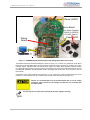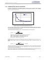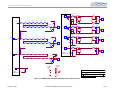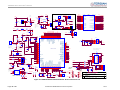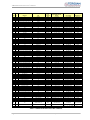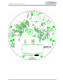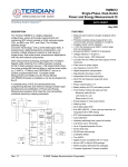
1
71M6534H Demo Board
USER’S MANUAL
5/28/2008 1:33:00 PM
V2-0
TERIDIAN Semiconductor Corporation
6440 Oak Canyon Rd., Suite 100
Irvine, CA 92618-5201
Phone: (714) 508-8800 ▪ Fax: (714) 508-8878
http://www.teridian.com/
[email protected]
71M6534H Demo Board User’s Manual
Page: 2 of 86
© 2005-2007 TERIDIAN Semiconductor Corporation
V2-0
71M6534H Demo Board User’s Manual
TERIDIAN Semiconductor Corporation makes no warranty for the use of its products, other than expressly contained in the Company’s
warranty detailed in the TERIDIAN Semiconductor Corporation standard Terms and Conditions. The company assumes no responsibility for any errors which may appear in this document, reserves the right to change devices or specifications detailed herein at
any time without notice and does not make any commitment to update the information contained herein.
Page: 3 of 86
© 2005-2007 TERIDIAN Semiconductor Corporation
V2-0
71M6534H Demo Board User’s Manual
71M6534H
3-Phase Energy Meter IC
DEMO BOARD
USER’S MANUAL
Page: 4 of 86
© 2005-2007 TERIDIAN Semiconductor Corporation
V2-0
71M6534H Demo Board User’s Manual
Table of Contents
1
GETTING STARTED................................................................................................................................................ 9
1.1
General .................................................................................................................................................................... 9
1.2
Safety and ESD Precautions ................................................................................................................................. 9
1.3
Demo Kit Contents ................................................................................................................................................. 9
1.4
Demo Board Versions .......................................................................................................................................... 10
1.5
Compatibility......................................................................................................................................................... 10
1.6
Suggested Equipment not Included ................................................................................................................... 10
1.7
Demo Board Test Setup ....................................................................................................................................... 10
1.7.1
Power Supply Setup ........................................................................................................................................ 13
1.7.2
Cable for Serial Connection (Debug Board) .................................................................................................... 13
1.7.3
Checking Operation......................................................................................................................................... 14
1.7.4
Serial Connection Setup.................................................................................................................................. 15
1.8
Using the Demo Board ......................................................................................................................................... 16
1.8.1
Serial Command Language ............................................................................................................................. 17
1.8.2
Using the Demo Board for Energy Measurements .......................................................................................... 25
1.8.3
Adjusting the Kh Factor for the Demo Board ................................................................................................... 25
1.8.4
Adjusting the Demo Boards to Different Current Transformers ....................................................................... 26
1.8.5
Adjusting the Demo Boards to Different Voltage Dividers ............................................................................... 26
1.9
Calibration Parameters ........................................................................................................................................ 27
1.9.1
General Calibration Procedure ........................................................................................................................ 27
1.9.2
Calibration Macro File ..................................................................................................................................... 28
1.9.3
Updating the 6534_demo.hex file .................................................................................................................... 28
1.9.4
Updating Calibration Data in Flash Memory without Using the ICE or a Programmer .................................... 28
1.9.5
Automatic Calibration (Auto-Cal) ..................................................................................................................... 29
1.9.6
Loading the 6534_demo.hex file into the Demo Board.................................................................................... 29
1.9.7
The Programming Interface of the 71M6534/6534H ....................................................................................... 31
1.10
Demo Code ........................................................................................................................................................ 32
1.10.1
Demo Code Description............................................................................................................................... 32
1.10.2
Important Demo Code MPU Parameters ..................................................................................................... 33
1.10.3
Useful CLI Commands Involving the MPU and CE ...................................................................................... 39
1.11
Using the ICE (In-Circuit Emulator) ................................................................................................................. 39
2
APPLICATION INFORMATION ............................................................................................................................. 41
2.1
Calibration Theory ................................................................................................................................................ 41
2.1.1
Calibration with Three Measurements ............................................................................................................. 41
2.1.2
Calibration with Five Measurements ............................................................................................................... 43
2.1.3
Fast Calibration ............................................................................................................................................... 44
2.2
Calibration Procedures ........................................................................................................................................ 45
2.2.1
Calibration Procedure with Three Measurements ........................................................................................... 46
2.2.2
Calibration Procedure with Five Measurements .............................................................................................. 47
2.2.3
Fast Calibration – Auto-Calibration.................................................................................................................. 47
2.2.4
Calibration Procedure for Rogowski Coil Sensors ........................................................................................... 48
2.2.5
Calibration Spreadsheets ................................................................................................................................ 49
2.2.6
Compensating for Non-Linearities ................................................................................................................... 52
2.3
Calibrating and Compensating the RTC ............................................................................................................. 53
2.4
Schematic Information ......................................................................................................................................... 54
2.4.1
Components for the V1 Pin ............................................................................................................................. 54
2.4.2
Reset Circuit .................................................................................................................................................... 54
2.4.3
Oscillator ......................................................................................................................................................... 55
Page: 5 of 86
© 2005-2007 TERIDIAN Semiconductor Corporation
V2-0
71M6534H Demo Board User’s Manual
2.4.4
EEPROM......................................................................................................................................................... 55
2.4.5
LCD ................................................................................................................................................................. 56
2.4.6
Optical Interface .............................................................................................................................................. 56
2.5
Testing the Demo Board ...................................................................................................................................... 57
2.5.1
Functional Meter Test...................................................................................................................................... 57
2.5.2
EEPROM......................................................................................................................................................... 58
2.5.3
RTC ................................................................................................................................................................. 59
2.5.4
Hardware Watchdog Timer (WDT) .................................................................................................................. 59
2.5.5
LCD ................................................................................................................................................................. 59
2.6
TERIDIAN Application Notes ............................................................................................................................... 60
3
HARDWARE DESCRIPTION................................................................................................................................. 61
3.1
D6534T14A2 Board Description: Jumpers, Switches and Test Points ............................................................ 61
3.2
Board Hardware Specifications .......................................................................................................................... 64
4
APPENDIX ............................................................................................................................................................. 65
4.1
D6534T14A2 Schematics, PCB Layout and BOM .............................................................................................. 66
4.2
Debug Board Description .................................................................................................................................... 76
4.3
71M6534H IC Description..................................................................................................................................... 81
4.4
Formulae for Fast Calibration ............................................................................................................................. 84
List of Figures
Figure 1-1: TERIDIAN D6534T14A2 Demo Board with Debug Board: Basic Connections ............................................... 11
Figure 1-2: Block diagram for the TERIDIAN D6534T14A2 Demo Board with Debug Board ............................................ 12
Figure 1-3: Hyperterminal Sample Window with Disconnect Button (Arrow) ..................................................................... 15
Figure 1-4: Port Speed and Handshake Setup (left) and Port Bit setup (right) .................................................................. 16
Figure 1-5: Command Line Help Display .......................................................................................................................... 17
Figure 1-6: Typical Calibration Macro File ......................................................................................................................... 28
Figure 1-7: Emulator Window Showing Reset and Erase Buttons (see Arrows) ............................................................... 30
Figure 1-8: Emulator Window Showing Erased Flash Memory and File Load Menu......................................................... 30
Figure 2-1: Watt Meter with Gain and Phase Errors.......................................................................................................... 41
Figure 2-2: Phase Angle Definitions .................................................................................................................................. 45
Figure 2-3: Calibration Spreadsheet for Three Measurements ......................................................................................... 50
Figure 2-4: Calibration Spreadsheet for Five Measurements ............................................................................................ 50
Figure 2-5: Calibration Spreadsheet for Rogowski coil ..................................................................................................... 51
Figure 2-6: Non-Linearity Caused by Quantification Noise ............................................................................................... 52
Figure 2-7: Voltage Divider for V1 ..................................................................................................................................... 54
Figure 2-8: External Components for RESET ................................................................................................................... 54
Figure 2-9: Oscillator Circuit .............................................................................................................................................. 55
Figure 2-10: EEPROM Circuit ........................................................................................................................................... 55
Figure 2-11: LCD Connections .......................................................................................................................................... 56
Figure 2-12: Optical Interface Block Diagram ................................................................................................................... 56
Figure 2-13: Meter with Calibration System ...................................................................................................................... 57
Figure 2-14: Calibration System Screen ........................................................................................................................... 58
Figure 3-1: D6534T14A2 Demo Board - Board Description (Default jumper settings indicated in yellow) ........................ 63
Figure 4-1: TERIDIAN D6534T14A2 Demo Board: Electrical Schematic 1/3 .................................................................... 66
Figure 4-2: TERIDIAN D6534T14A2 Demo Board: Electrical Schematic 2/3 .................................................................... 67
Figure 4-3: TERIDIAN D6534T14A2 Demo Board: Electrical Schematic 3/3 .................................................................... 68
Figure 4-4: TERIDIAN D6534T14A2 Demo Board: Top View ........................................................................................... 70
Figure 4-5: TERIDIAN D6534T14A2 Demo Board: Bottom View ...................................................................................... 71
Page: 6 of 86
© 2005-2007 TERIDIAN Semiconductor Corporation
V2-0
71M6534H Demo Board User’s Manual
Figure 4-6: TERIDIAN D6534T14A2 Demo Board: Top Signal Layer ............................................................................... 72
Figure 4-7: TERIDIAN D6534T14A2 Demo Board: Bottom Signal Layer .......................................................................... 75
Figure 4-8: TERIDIAN D6534T14A2 Demo Board: Ground Layer .................................................................................... 73
Figure 4-9: TERIDIAN D6534T14A2 Demo Board: V3P3 Layer ....................................................................................... 74
Figure 4-10: Debug Board: Electrical Schematic............................................................................................................... 77
Figure 4-11: Debug Board: Top View ................................................................................................................................ 78
Figure 4-12: Debug Board: Bottom View........................................................................................................................... 78
Figure 4-13: Debug Board: Top Signal Layer .................................................................................................................... 79
Figure 4-14: Debug Board: Middle Layer 1 (Ground Plane) .............................................................................................. 79
Figure 4-15: Debug Board: Middle Layer 2 (Supply Plane) ............................................................................................... 80
Figure 4-16: Debug Board: Bottom Trace Layer ............................................................................................................... 80
Figure 4-17: TERIDIAN 71M6534H epLQFP100: Pinout (top view) .................................................................................. 83
List of Tables
Table 1-1: Jumper settings on Debug Board ..................................................................................................................... 13
Table 1-2: Straight cable connections ............................................................................................................................... 13
Table 1-3: Null-modem cable connections ........................................................................................................................ 13
Table 1-4: Selectable Display Parameters ........................................................................................................................ 14
Table 1-5: CE RAM Locations for Calibration Constants .................................................................................................. 27
Table 1-6: Flash Programming Interface Signals .............................................................................................................. 31
Table 1-7: MPU Input Parameters for Metering ................................................................................................................ 34
Table 1-8: Selectable Pulse Sources ................................................................................................................................ 35
Table 1-9: MPU Instantaneous Output Variables .............................................................................................................. 36
Table 1-10: MPU Status Word Bit Assignment.................................................................................................................. 37
Table 1-11: MPU Accumulation Output Variables ............................................................................................................. 38
Table 1-12: CLI Commands for MPU Data Memory.......................................................................................................... 39
Table 3-1: D6534T14A2 Demo Board Description ............................................................................................................ 61
Table 4-1: D6534T14A2 Demo Board: Bill of Material ...................................................................................................... 69
Table 4-2: Debug Board: Bill of Material ........................................................................................................................... 76
Page: 7 of 86
© 2005-2007 TERIDIAN Semiconductor Corporation
V2-0
71M6534H Demo Board User’s Manual
Page: 8 of 86
© 2005-2007 TERIDIAN Semiconductor Corporation
V2-0
71M6534H Demo Board User’s Manual
1
1
GETTING STARTED
1.1
GENERAL
The TERIDIAN Semiconductor Corporation (TSC) 71M6534H Demo Board is a demonstration board for
evaluating the 71M6534H device for 3-phase electronic power metering applications. It incorporates a 71M6534
or 71M6534H integrated circuit, peripheral circuitry such as a serial EEPROM, emulator port, and on board
power supply as well as a companion Debug Board that allows a connection to a PC through a RS232 port. The
demo board allows the evaluation of the 71M6534 or 71M6534H energy meter chip for measurement accuracy
and overall system use.
The board is pre-programmed with a Demo Program in the FLASH memory of the 71M6534/6534H IC. This embedded application is developed to exercise all low-level function calls to directly manage the peripherals, flash
programming, and CPU (clock, timing, power savings, etc.).
The 71M6534/6534H IC on the Demo Board is pre-programmed with default calibration factors.
1.2
SAFETY AND ESD PRECAUTIONS
Connecting live voltages to the demo board system will result in potentially hazardous voltages on the demo
board.
THE DEMO SYSTEM IS ESD SENSITIVE! ESD PRECAUTIONS SHOULD BE TAKEN
WHEN HANDLING THE DEMO BOARD!
EXTREME CAUTION SHOULD BE TAKEN WHEN HANDLING THE DEMO BOARD
ONCE IT IS CONNECTED TO LIVE VOLTAGES!
1.3
DEMO KIT CONTENTS
•
•
•
•
•
Demo Board D6534T14A2 with 71M6534H IC and pre-loaded demo program:
Debug Board
Two 5VDC/1,000mA universal wall transformers with 2.5mm plug (Switchcraft 712A compatible)
Serial cable, DB9, Male/Female, 2m length (Digi-Key AE1020-ND)
CD-ROM containing documentation (data sheet, board schematics, BOM, layout), Demo Code (sources
and executable), and utilities
The CD-ROM contains a file named readme.txt that describes all files found on the CD-ROM.
Page: 9 of 86
© 2005-2007 TERIDIAN Semiconductor Corporation
V2-0
71M6534H Demo Board User’s Manual
1.4
DEMO BOARD VERSIONS
At printing time of this document only the following version of the Demo Board is available:
•
1.5
Demo Board D6534T14A2 (standard)
COMPATIBILITY
This manual applies to the following hardware and software revisions:
•
•
•
1.6
71M6534 or 71M6534H chip revision A03
Demo Kit firmware revision 4p6q
Demo Boards D6534T14A2
SUGGESTED EQUIPMENT NOT INCLUDED
For functional demonstration:
•
PC w/ MS-Windows® versions XP, ME, or 2000, equipped with RS232 port (COM port) via DB9 connector
For software development (MPU code):
1.7
•
Signum ICE (In Circuit Emulator): ADM-51 – see update information in section 1.11
http://www.signum.com
•
Keil 8051 “C” Compiler kit: CA51
http://www.keil.com/c51/ca51kit.htm, http://www.keil.com/product/sales.htm
DEMO BOARD TEST SETUP
Figure 1-1 shows the basic connections of the Demo Board plus Debug Board with the external equipment for
desktop testing, i.e. without live power applied. For desktop testing, both the Demo and Debug board may be
powered with their 5VDC power supplies.
Page: 10 of 86
© 2005-2007 TERIDIAN Semiconductor Corporation
V2-0
71M6534H Demo Board User’s Manual
Power (5VDC)
Demo Board
Two Power Supplies
(100VAC to 240VAC,
5V/1ADC Output)
Power 5VDC
Debug
Board
Host PC
Figure 1-1: TERIDIAN D6534T14A2 Demo Board with Debug Board: Basic Connections
The D6534T14A2 Demo Board block diagram is shown in Figure 1-2. It consists of a stand-alone meter Demo
Board and an optional Debug Board. The Demo Board contains all circuits necessary for operation as a meter,
including display, calibration LED, and internal power supply. The Debug Board provides magnetic isolation
from the meter and interfaces to a PC through a 9 pin serial port. For serial communication between the PC and
the TERIDIAN 71M6534H, the Debug Board needs to be plugged with its connector J3 into connector J2 of the
Demo Board.
Connections to the external signals to be measured, i.e. AC voltages and current signals derived from shunt
resistors or current transformers, are provided on the rear side of the demo board (see Figure 3-1).
Caution: It is recommended to set up the demo board with no live AC voltage
connected, and to connect live AC voltages only after the user is familiar with
the demo system.
All input signals are referenced to the V3P3 (3.3V power supply to the chip).
Page: 11 of 86
© 2005-2007 TERIDIAN Semiconductor Corporation
V2-0
71M6534H Demo Board User’s Manual
DEMONSTRATION METER
External Current
Transformers
PULSE OUTPUTS
DIO6/WPULSE
IDN
IAP
IA
DIO8/XPULSE
DIO7/RPULSE
IAN
IBP
IB
VARh
V3P3SYS
V3P3SYS
DIO9/YPULSE
3.3V LCD
IBN
ICP
IC
DIO4
ICN
V3P3A
DIO5
V3P3SYS
6534H
Single Chip
VA
Meter
VB
VC
DIO56
VC
VB
VA
JP1
V3P3
NEUTRAL
Wh
IDP
INEUTRAL
3.3v
DIO57
GND
GND
DIO58
TX
5V DC
JP8
RX
VBAT
battery
(optional)
PB
ICE Connector
DEBUG BOARD (OPTIONAL)
MPU HEARTBEAT (5Hz)
1
OPTO
2
V5_DBG
CE HEARTBEAT (1Hz)
V5_DBG
OPTO
3
OPTO
10
OPTO
12
8
CKTEST
6
DB9
to PC
COM Port
RS-232
INTERFACE
OPTO
RTM INTERFACE
GND 5, 7,
9, 11
TMUXOUT
GND_DBG
V5_DBG
OPTO
FPGA
J5
PB
V3P3D
On-board
components
powered by
V3P3D
EEPROM
6
68 Pin Connector
to NI PCI-6534
DIO Board
OPTO
4
V5_DBG
15, 16
N/C
13, 14
N/C
J2
5V DC
V5_NI
GND_DBG
JP21
05/23/2008
Figure 1-2: Block diagram for the TERIDIAN D6534T14A2 Demo Board with Debug Board
Page: 12 of 86
© 2005-2007 TERIDIAN Semiconductor Corporation
V2-0
71M6534H Demo Board User’s Manual
1.7.1 POWER SUPPLY SETUP
There are several choices for meter power supply:
•
•
•
Internal (using phase A of the AC line voltage). The internal power supply is only suitable when phase A
exceeds 220V RMS.
External 5VDC connector (J1) on the Demo Board
External 5VDC connector (J1) on the Debug Board.
The power supply jumper JP1 must be consistent with the power supply choice. JP1 connects the AC line
voltage to the internal power supply. This jumper should usually be left in place.
1.7.2 CABLE FOR SERIAL CONNECTION (DEBUG BOARD)
For connection of the DB9 serial port to a PC, either a straight or a so-called “null-modem” cable may be used.
JP1 and JP2 are plugged in for the straight cable, and JP3/JP4 are empty. The jumper configuration is reversed
for the null-modem cable, as shown in Table 1-1.
Cable
Configuration
Mode
Straight Cable
Null-Modem Cable
Jumpers on Debug Board
JP1
JP2
JP3
JP4
Default
Installed
Installed
--
--
Alternative
--
--
Installed
Installed
Table 1-1: Jumper settings on Debug Board
JP1 through JP4 can also be used to alter the connection when the PC is not configured as a DCE device.
Table 1-2 shows the connections necessary for the straight DB9 cable and the pin definitions.
PC Pin
Function
Demo Board Pin
2
TX
2
3
RX
3
5
Signal Ground
5
Table 1-2: Straight cable connections
Table 1-3 shows the connections necessary for the null-modem DB9 cable and the pin definitions.
PC Pin
Function
Demo Board Pin
2
TX
3
3
RX
2
5
Signal Ground
5
Table 1-3: Null-modem cable connections
Page: 13 of 86
© 2005-2007 TERIDIAN Semiconductor Corporation
V2-0
71M6534H Demo Board User’s Manual
1.7.3 CHECKING OPERATION
A few seconds after power up, the LCD display on the Demo Board should display this brief greeting:
H
E
L
L
0
The “HELLO” message should be followed by the display of accumulated energy alternating with the text “Wh”.
3.
0.
W
0
0
1
h
If the PB switch on the Demo Board is pressed and held down), the display will cycle through a series of
parameters, as shown in Table 1-4.
Step
Displayed
Text
Step
Displayed
Text
1
DELTA C
Deviation from nominal
temperature [°C]
10
DATE
2
HZ
Line frequency [Hz]
11
PF
3
Wh
Accumulated real energy
[Wh]
12
4
Wh
Exported real energy [Wh]
13
EDGES
5
VARh
Accumulated reactive energy
[VARh]
14
PULSES
6
VARh
Exported reactive energy
[VARh]
15
A
Current
7
VAh
Accumulated apparent
energy [VARh]
16
V
Voltage
8
HOURS
Hours of operation since last
reset [1/100 h]
17
VBAT
9
TIME
Real time from RTC
[hh.mm.ss]
--
--
Description
Description
Date from RTC [yyyy.mm.dd]
Power factor, calculated from current
Wh/VAh
Accumulated pulses
Battery voltage
--
Table 1-4: Selectable Display Parameters
Once, the Debug Board is plugged into J2 of the Demo Board, LED DIO1 on the Debug Board will flash with a
frequency of 1Hz, indicating CE activity. The LED DIO0 will flash with a frequency of 5Hz, indicating MPU
activity.
Page: 14 of 86
© 2005-2007 TERIDIAN Semiconductor Corporation
V2-0
71M6534H Demo Board User’s Manual
1.7.4 SERIAL CONNECTION SETUP
After connecting the DB9 serial port to a PC, start the HyperTerminal application and create a session using the
following parameters:
Port Speed: 9600 bd or 300bd, depending on jumper JP16 (see section 3.1)
Data Bits: 8
Parity: None
Stop Bits: 1
Flow Control: XON/XOFF
HyperTerminal can be found by selecting Programs ÆAccessories Æ Communications from the Windows©
start menu. The connection parameters are configured by selecting File Æ Properties and then by pressing the
Configure button. Port speed and flow control are configured under the General tab (Figure 1-4, left), bit settings
are configured by pressing the Configure button (Figure 1-5, right), as shown below. A setup file (file name
“Demo Board Connection.ht”) for HyperTerminal that can be loaded with File Æ Open is also provided with the
tools and utilities.
Port parameters can only be adjusted when the connection is not active. The disconnect
button, as shown in Figure 1-3 must be clicked in order to disconnect the port.
Figure 1-3: Hyperterminal Sample Window with Disconnect Button (Arrow)
Page: 15 of 86
© 2005-2007 TERIDIAN Semiconductor Corporation
V2-0
71M6534H Demo Board User’s Manual
Figure 1-4: Port Speed and Handshake Setup (left) and Port Bit setup (right)
Once, the connection to the demo board is established, press <CR> and the prompt, >, should appear. Type >?
to see the Demo Code help menu. Type >i to verify the Demo Code revision.
1.8
USING THE DEMO BOARD
The 71M6534/6534H Demo Board is a ready-to-use meter prepared for use with external current transformers.
Using the Demo Board involves communicating with the Demo Code via the command line interface (CLI). The
CLI allows modifications to the metering parameters, access to the EEPROM, initiation of auto-cal sequences,
selection of the displayed parameters, changing of calibration factors and more operations that can be used to
evaluate the 71M6534 chip.
Before evaluating the 71M6534/6534H on the Demo Board, users should get familiar with the commands and
responses of the CLI. A complete description of the CLI is provided in section 1.8.1.
Page: 16 of 86
© 2005-2007 TERIDIAN Semiconductor Corporation
V2-0
71M6534H Demo Board User’s Manual
1.8.1 SERIAL COMMAND LANGUAGE
The Demo Code residing in the flash memory of the 71M6534/6534H provides a convenient way of examining
and modifying key meter parameters. Once the Demo Board is connected to a PC or terminal per the
instructions given in Section 1.7.2 and 1.7.4, typing ‘?’ will bring up the list of commands shown in Figure 1-5.
Figure 1-5: Command Line Help Display
The tables in this chapter describe the commands in detail.
Page: 17 of 86
© 2005-2007 TERIDIAN Semiconductor Corporation
V2-0
71M6534H Demo Board User’s Manual
Commands to Display Help on the CLI Commands:
?
HELP
Description:
Command
combinations:
Examples:
Comment
Command help available for each of the options below.
?
Command line interpreter help menu.
?]
Display help on access CE data RAM
?)
Display help on access MPU RAM
?,
Display help on repeat last command
?/
Display help on ignore rest of line
?C
Display help on compute engine control.
?CL
Display help on calibration.
?EE
Display help on EEPROM control
?ER
Display help on error recording
?I
Display help on information message
?M
Display help on meter display control
?MR
Display help on meter RMS display control
?R
Display help on SFR control
?RT
Display help on RTC control
?T
Display help on trim control
?W
Display help on the wait/reset command
?Z
Display help on reset
??
Display the command line interpreter help menu.
?C
Displays compute engine control help.
Commands for CE Data Access:
]
CE DATA ACCESS
Description:
Usage:
Command
combinations:
Allows user to read from and write to CE data space.
] [Starting CE Data Address] [option]…[option]
]A???
Read consecutive 16-bit words in Decimal, starting at
address A
]A$$$
Read consecutive 16-bit words in Hex, starting at
address A
]A=n=n
]U
Example:
Comment
]40$$$
Write consecutive memory values, starting at address
A
Update default version of CE Data in flash memory
Reads CE data words 0x40, 0x41 and 0x42.
]7E=12345678=9876ABCD
Writes two words starting @ 0x7E
All CE data words are in 4-byte (32-bit) format. Typing ]A? will access the 32-bit word located at the byte
address 0x1000 + 4 * A = 0x1028.
Page: 18 of 86
© 2005-2007 TERIDIAN Semiconductor Corporation
V2-0
71M6534H Demo Board User’s Manual
Commands for MPU/XDATA Access:
)
MPU DATA ACCESS
Description:
Usage:
Command
combinations:
Allows user to read from and write to MPU data space.
) [Starting MPU Data Address] [option]…[option]
)A???
Read three consecutive 32-bit words in Decimal,
starting at address A
)A$$$
Read three consecutive 32-bit words in Hex, starting at
address A
)A=n=m
?)
Example:
Comment
)08$$$$
Write the values n and m to two consecutive
addresses starting at address A
Display useful RAM addresses.
Reads data words 0x08, 0x0C, 0x10, 0x14
)04=12345678=9876ABCD
Writes two words starting @ 0x04
MPU or XDATA space is the address range for the MPU XRAM (0x0000 to 0xFFF). All MPU data words are in
4-byte (32-bit) format. Typing ]A? will access the 32-bit word located at the byte address 4 * A = 0x28. The
energy accumulation registers of the Demo Code can be accessed by typing two Dollar signs (“$$”), typing
question marks will display negative decimal values if the most significant bit is set.
Commands for DIO RAM (Configuration RAM) and SFR Control:
R
DIO AND SFR CONTROL
Description:
Usage:
Command
combinations:
Example:
Comment
Allows the user to read from and write to DIO RAM and special function registers (SFRs).
R [option] [register] … [option]
RIx…
Select I/O RAM location x (0x2000 offset is
automatically added)
Rx…
Select internal SFR at address x
Ra???...
Read consecutive SFR registers in Decimal, starting at
address a
Ra$$$...
Read consecutive registers in Hex, starting at address
a
Ra=n=m…
Set values of consecutive registers to n and m starting
at address a
RI2$$$
Read DIO RAM registers 2, 3, and 4 in Hex.
DIO or Configuration RAM space is the address range 0x2000 to 0x20FF. This RAM contains registers used for configuring
basic hardware and functional properties of the 71M6534/6534H and is organized in bytes (8 bits). The 0x2000 offset is
automatically added when the command RI is typed.
The SFRs (special function registers) are located in internal RAM of the 80515 core, starting at address 0x80.
Page: 19 of 86
© 2005-2007 TERIDIAN Semiconductor Corporation
V2-0
71M6534H Demo Board User’s Manual
Commands for EEPROM Control:
EE
EEPROM CONTROL
Description:
Comment
Allows user to enable read and write to EEPROM.
Usage:
EE [option] [arguments]
Command
combinations:
EECn
EEPROM Access (1 Æ Enable, 0 Æ Disable)
EERa.b
Read EEPROM at address 'a' for 'b' bytes.
EESabc..xyz
Write characters to buffer (sets Write length)
EETa
Transmit buffer to EEPROM at address 'a'.
EEWa.b...z
Write values to buffer
Example:
CLS
Saves calibration to EEPROM
EEShello
EET$0210
Writes 'hello' to buffer, then transmits buffer to
EEPROM starting at address 0x210.
Due to buffer size restrictions, the maximum number of bytes handled by the EEPROM command is
0x40.
Auxiliary Commands:
Typing a comma (“,”) repeats the command issued from the previous command line. This is very helpful when
examining the value at a certain address over time, such as the CE DRAM address for the temperature (0x40).
The slash (“/”) is useful to separate comments from commands when sending macro text files via the serial
interface. All characters in a line after the slash are ignored.
Commands controlling the CE, TMUX and the RTM:
C
COMPUTE ENGINE
CONTROL
Description:
Comment
Allows the user to enable and configure the compute engine.
Usage:
C [option] [argument]
Command
combinations:
CEn
Compute Engine Enable (1 Æ Enable,
0 Æ Disable)
CTn
Select input n for TMUX output pin. n is interpreted as
a decimal number.
CREn
CRSa.b.c.d
Example:
Page: 20 of 86
RTM output control (1 Æ Enable, 0 Æ Disable)
Selects CE addresses for RTM output
CE0
Disables CE, followed by “CE OFF” display on LCD.
The Demo Code will reset if the WD timer is enabled.
CT3
Selects the VBIAS signal for the TMUX output pin
© 2005-2007 TERIDIAN Semiconductor Corporation
V2-0
71M6534H Demo Board User’s Manual
Commands controlling the Auto-Calibration Function:
CL
AUTO-CALIBRATION
CONTROL
Description:
Comment
Allows the user to initiate auto-calibration and to store calibration values.
Usage:
CL [option]
Command
combinations:
CLB
Begin auto-calibration. Prior to auto-calibration, the
calibration coefficients are automatically restored from
flash memory.
CLS
Save calibration coefficients to EEPROM starting at
address 0x0004
CLR
Restore calibration coefficients from EEPROM
CLD
Restore coefficients from flash memory
CLB
Starts auto-calibration and saves data automatically.
Example:
Before starting the auto-calibration process, target values for voltage, duration and current must be entered in
MPU RAM (see section 1.9.5), and the target voltage and current must be applied constantly during calibration.
Calibration factors can be saved to EEPROM using the CLS command.
Commands controlling the Pulse Counter Function
CP
PULSE-COUNT CONTROL
Description:
Comment
Allows the user to control the pulse count functions.
Usage:
CP [option]
Command
combinations:
CPA
Start pulse counting for time period defined with the
CPD command. Pulse counts will display with
commands M15.2, M16.2
CPC
Clear the absolute pulse count displays (shown with
commands M15.1, M16.1)
CPDn
Set time window for pulse counters to n seconds, n is
interpreted as a decimal number.
CPD60
Set time window to 60 seconds.
Example:
Pulse counts accumulated over a time window defined by the CPD command will be displayed by M15.2 or
M16.2 after the defined time has expired.
Commands M15.1 and M16.1 will display the absolute pulse count for the W and VAR outputs. These displays are reset to
zero with the CPC command (or the XRAM write )1=2).
Commands M15.2 and M16.2 will display the number of pulses counted during the interval defined by the CPD
command. These displays are reset only after a new reading, as initiated by the CPA command.
Commands for Identification and Information:
I
INFORMATION MESSAGES
Description:
Usage:
Comment
Allows user to read information messages.
I
Displays complete version information
The I command is mainly used to identify the revisions of Demo Code and the contained CE code.
Commands for Controlling the RMS Values Shown on the LCD Display:
MR
Page: 21 of 86
METER RMS DISPLAY
Comment
© 2005-2007 TERIDIAN Semiconductor Corporation
V2-0
71M6534H Demo Board User’s Manual
CONTROL (LCD)
Description:
Allows user to select meter RMS display for voltage or current.
Usage:
MR [option]. [option]
Command
combinations:
MR1. [phase]
Displays instantaneous RMS current
MR2. [phase]
Displays instantaneous RMS voltage
Example:
MR1.3
Displays phase C RMS current.
Phase 4 is the measured neutral current.
No error message is issued when an invalid parameter is entered, e.g. MR1.8.
Commands for Controlling the MPU Power Save Mode:
PS
POWER SAVE MODE
Description:
Enters power save mode
Comment
Disables CE, ADC, CKOUT, ECK, RTM, SSI, TMUX
VREF, and serial port, sets MPU clock to 38.4KHz.
Usage:
PS
Return to normal mode is achieved by resetting the MPU (Z command).
Commands for Controlling the RTC:
RT
REAL TIME CLOCK
CONTROL
Description:
Allows the user to read and set the real time clock.
Usage:
RT [option] [value] … [value]
Command
combinations:
RTDy.m.d.w: Day of week
RTR
RTTh.m.s
RTAs.t
Example:
Comment
RTD05.03.17.5
RTA1.+1234
(year, month, day, weekday [1 = Sunday]). If the
weekday is omitted it is set automatically.
Read Real Time Clock.
Time of day: (hr, min, sec).
Real Time Adjust: (start, trim). Allows trimming of the
RTC.
If s > 0, the speed of the clock will be adjusted by ‘t’
parts per billion (PPB). If the CE is on, the value
entered with 't' will be changing with temperature, based
on Y_CAL, Y_CALC and Y_CALC2.
Programs the RTC to Thursday, 3/17/2005
Speeds up the RTC by 1234 PPB.
The “Military Time Format” is used for the RTC, i.e. 15:00 is 3:00 PM.
Page: 22 of 86
© 2005-2007 TERIDIAN Semiconductor Corporation
V2-0
71M6534H Demo Board User’s Manual
Commands for Accessing the Trim Control Registers:
T
TRIM CONTROL
Description:
Comment
Allows user to read trim and fuse values.
Usage:
T [option]
Command
combinations:
T4
Read fuse 4 (TRIMM).
T5
Read fuse 5 (TRIMBGA)
T6
Read fuse 6 (TRIMBGB).
Example:
T4
Reads the TRIMM fuse.
These commands are only accessible for the 71M6534H (0.1%) parts. When used on a 71M6534
(0.5%) part, the results will be displayed as zero.
Reset Commands:
W
RESET
Description:
Usage:
Page: 23 of 86
Comment
Watchdog control
W
Halts the Demo Code program, thus suppressing the
triggering of the hardware watchdog timer. This will
cause a reset, if the watchdog timer is enabled.
© 2005-2007 TERIDIAN Semiconductor Corporation
V2-0
71M6534H Demo Board User’s Manual
Commands for Controlling the Metering Values Shown on the LCD Display:
M
METER DISPLAY
CONTROL (LCD)
Description:
Comment
Allows user to select internal variables to be displayed.
Usage:
M [option]. [option]
Command
combinations:
M
Wh Total Consumption (display wraps around at 999.999)
M0
Wh Total Consumption (display wraps around at 999.999)
M1
Temperature (C° delta from nominal)
M2
Frequency (Hz)
M3. [phase]
Wh Total Consumption (display wraps around at 999.999)
M4. [phase]
Wh Total Inverse Consumption (display wraps around at 999.999)
M5. [phase]
VARh Total Consumption (display wraps around at 999.999)
M6. [phase]
VARh Total Inverse Consumption (display wraps around at
999.999)
M7. [phase]
VAh Total (display wraps around at 999.999)
M8
Operating Time (in hours)
M9
Real Time Clock
M10
Calendar Date
M11. [phase]
M13
Example:
Power factor
Mains edge count for the last accumulation interval
M13.1
Main edge count (accumulated) – zero transitions of the input
signal
M13.2
CE main edge count for the last accumulation interval
M14.1
Absolute count for W pulses. Reset with CPC command.
M14.2
Count for W pulses in time window defined by the CPD command.
M15.1
Absolute count for VAR pulses. Reset with CPC command.
M15.2
Count for W pulses in time window defined by the CPD command.
M3.3
Displays Wh total consumption of phase C.
M5.0
Displays VARh total consumption for all phases.
Displays for total consumption wrap around at 999.999Wh (or VARh, VAh) due to the limited
number of available display digits. Internal registers (counters) of the Demo Code are 64 bits
wide and do not wrap around.
When entering the phase parameter, use 1 for phase A, 2 for phase B, 3 for phase C, and 0 or
blank for all phases.
Page: 24 of 86
© 2005-2007 TERIDIAN Semiconductor Corporation
V2-0
71M6534H Demo Board User’s Manual
1.8.2 USING THE DEMO BOARD FOR ENERGY MEASUREMENTS
The 71M6534/6534H Demo Board was designed for use with current transformers (CT).
The Demo Board may immediately be used with current transformers having 2,000:1 winding ratio and is
programmed for a Kh factor of 3.2 and (see Section 1.8.4 for adjusting the Demo Board for transformers with
different turns ratio).
Once, voltage is applied and load current is flowing, the red LED D5 will flash each time an energy sum of 3.2
Wh is collected. The LCD display will show the accumulated energy in Wh when set to display mode 3
(command >M3 via the serial interface).
Similarly, the red LED D6 will flash each time an energy sum of 3.2 VARh is collected. The LCD display will
show the accumulated energy in VARh when set to display mode 5 (command >M5 via the serial interface).
1.8.3 ADJUSTING THE KH FACTOR FOR THE DEMO BOARD
The 71M6534/6534H Demo Board is shipped with a pre-programmed scaling factor Kh of 3.2, i.e. 3.2Wh per
pulse. In order to be used with a calibrated load or a meter calibration system, the board should be connected
to the AC power source using the spade terminals on the bottom of the board. The current transformers should
be connected to the dual-pin headers on the bottom of the board. The connection is the same for single-ended
or differential mode. See chapter 3.1 for proper jumper settings.
The Kh value can be derived by reading the values for IMAX and VMAX (i.e. the RMS current and voltage
values that correspond to the 250mV maximum input signal to the IC), and inserting them in the following
equation for Kh:
Kh = IMAX * VMAX * 66.1782 / (In_8 * WRATE * NACC * X) = 3.19902 Wh/pulse.
The small deviation between the adjusted Kh of 3.19902 and the ideal Kh of 3.2 is covered by calibration. The
default values used for the 71M6534/6534H Demo Board are:
WRATE:
IMAX:
VMAX:
In_8:
NACC:
X:
171
208
600
1
2520
6
(controlled by IA_SHUNT = -15)
Explanation of factors used in the Kh calculation:
WRATE:
The factor input by the user to determine Kh
IMAX:
The current input scaling factor, i.e. the input current generating 176.8mVrms at the IA/IB/IC
input pins of the 71M6534. 176.8mV rms is equivalent to 250mV peak.
VMAX:
The voltage input scaling factor, i.e. the voltage generating 176.8mVrms at the VA/VB/VC
input pins of the 71M6534
In_8:
The setting for the additional ADC gain (8 or 1) determined by the CE register IA_SHUNT
NACC:
The number of samples per accumulation interval, i.e. PRE_SAMPS *SUM_CYCLES
X:
The pulse rate control factor determined by the CE registers PULSE_SLOW and
PULSE_FAST
Almost any desired Kh factor can be selected for the Demo Board by resolving the formula for WRATE:
WRATE = (IMAX * VMAX * 66.1782) / (Kh * In_8 * NACC * X)
For the Kh of 3.2Wh, the value 171 (decimal) should be entered for WRATE at CE location 0x21 (using the CLI
command >]21=+171).
Page: 25 of 86
© 2005-2007 TERIDIAN Semiconductor Corporation
V2-0
71M6534H Demo Board User’s Manual
1.8.4 ADJUSTING THE DEMO BOARDS TO DIFFERENT CURRENT TRANSFORMERS
The Demo Board is prepared for use with 2000:1 current transformers (CTs). This means that for the unmodified Demo Board, 208A on the primary side at 2000:1 ratio result in 104mA on the secondary side, causing
176.8mV at the 1.7Ω resistor pairs R24/R25, R36/R37, R56/R57 (2 x 3.4Ω in parallel).
In general, when IMAX is applied to the primary side of the CT, the voltage Vin at the IA, IB, or IC input of the
71M6534 IC is determined by the following formula:
Vin = R * I = R * IMAX/N
where N = transformer winding ratio, R = resistor on the secondary side
If, for example, if the current corresponding to IMAX = 208A is applied to a CT with a 2500:1 ratio, only 83.2mA
will be generated on the secondary side, causing only 141mV of voltage drop.
The steps required to adapt a 71M6534 Demo Board to a transformer with a winding ratio of 2500:1 are outlined
below:
1)
2)
The formula Rx = 176.8mV/(IMAX/N) is applied to calculate the new resistor Rx. We calculate Rx to 2.115Ω
Changing the resistors R24/R25, R106/R107 to a combined resistance of 2.115Ω (for each pair) will
cause the desired voltage drop of 176.8mV appearing at the IA, IB, or IC inputs of the 71M6534 IC.
Simply scaling IMAX is not recommended, since peak voltages at the 71M6534 inputs should always be in the
range of 0 through ±250mV (equivalent to 176.8mV rms). If a CT with a much lower winding ratio than 1:2,000
is used, higher secondary currents will result, causing excessive voltages at the 71M6534 inputs. Conversely,
CTs with much higher ratio will tend to decrease the useable signal voltage range at the 71M6534 inputs and
may thus decrease resolution.
1.8.5 ADJUSTING THE DEMO BOARDS TO DIFFERENT VOLTAGE DIVIDERS
The 71M6534 Demo Board comes equipped with its own network of resistor dividers for voltage measurement
mounted on the PCB. The resistor values are 2.5477MΩ (for channel A, R15-R21, R26-R31 combined) and
750Ω (R32), resulting in a ratio (RR) of 1:3,393.933. This means that VMAX equals 176.78mV*3,393.933 =
600V. A large value for VMAX has been selected in order to have headroom for overvoltages. This choice need
not be of concern, since the ADC in the 71M6534 has enough resolution, even when operating at 120Vrms.
If a different set of voltage dividers or an external voltage transformer (potential transformer) is to be used,
scaling techniques similar to those applied for the current transformer should be used.
In the following example we assume that the line voltage is not applied to the resistor divider for VA formed by
R15-R21, R26-R31, and R32, but to a voltage transformer with a ratio N of 20:1, followed by a simple resistor
divider. We also assume that we want to maintain the value for VMAX at 600V to provide headroom for large
voltage excursions.
When applying VMAX at the primary side of the transformer, the secondary voltage Vs is:
Vs = VMAX / N
Vs is scaled by the resistor divider ratio RR. When the input voltage to the voltage channel of the 71M6534 is the
desired 176.8mV, Vs is then given by:
Vs = RR * 176.8mV
Resolving for RR, we get:
RR = (VMAX / N) / 176.8mV = (600V / 30) / 176.8mV = 170.45
This divider ratio can be implemented, for example, with a combination of one 16.95kΩ and one 100Ω resistor.
Page: 26 of 86
© 2005-2007 TERIDIAN Semiconductor Corporation
V2-0
71M6534H Demo Board User’s Manual
If potential transformers (PTs) are used instead of resistor dividers, phase shifts will be introduced that will require negative phase angle compensation. TERIDIAN Demo Code accepts negative calibration factors for
phase.
1.9
CALIBRATION PARAMETERS
1.9.1 GENERAL CALIBRATION PROCEDURE
Any calibration method can be used with the 71M6534/6534H chips. This Demo Board User’s Manual presents
calibration methods with three or five measurements as recommended methods, because they work with most
manual calibration systems based on counting "pulses" (emitted by LEDs on the meter).
Naturally, a meter in mass production will be equipped with special calibration code offering capabilities beyond
those of the Demo Code. It is basically possible to calibrate using voltage and current readings, with or without
pulses involved. For this purpose, the MPU Demo Code can be modified to display averaged voltage and
current values (as opposed to momentary values). Also, automated calibration equipment can communicate
with the Demo Boards via the serial interface and extract voltage and current readings. This is possible even
with the unmodified Demo Code.
A complete calibration procedure is given in section 2.2 of this manual.
Regardless of the calibration procedure used, parameters (calibration factors) will result that will have to be
applied to the 71M6534/6534H chip in order to make the chip apply the modified gains and phase shifts
necessary for accurate operation. Table 1-5 shows the names of the calibration factors, their function, and their
location in the CE RAM.
Again, the command line interface can be used to store the calibration factors in their respective CE RAM
addresses. For example, the command
>]10=+16302
stores the decimal value 16302 in the CE RAM location controlling the gain of the current channel (CAL_IA) for
phase A.
The command
>]11=4005
stores the hexadecimal value 0x4005 (decimal 16389) in the CE RAM location controlling the gain of the
voltage channel for phase A (CAL_VA).
Constant
CE
Address
(hex)
CAL_VA
CAL_VB
CAL_VC
0x11
0x13
0x15
Adjusts the gain of the voltage channels. +16384 is the typical value. The
gain is directly proportional to the CAL parameter. Allowed range is 0 to
32767. If the gain is 1% slow, CAL should be increased by 1%.
CAL_IA
CAL_IB
CAL_IC
0x10
0x12
0x14
Adjusts the gain of the current channels. +16384 is the typical value. The
gain is directly proportional to the CAL parameter. Allowed range is 0 to
32767. If the gain is 1% slow, CAL should be increased by 1%.
PHADJ_A
PHADJ_B
PHADJ_C
0x18
0x19
0x1A
This constant controls the CT phase compensation. No compensation
occurs when PHADJ=0. As PHADJ is increased, more compensation is
introduced.
Description
Table 1-5: CE RAM Locations for Calibration Constants
Page: 27 of 86
© 2005-2007 TERIDIAN Semiconductor Corporation
V2-0
71M6534H Demo Board User’s Manual
1.9.2 CALIBRATION MACRO FILE
The macro file in Figure 1-6 contains a sequence of the serial interface commands. It is a simple text file and
can be created with Notepad or an equivalent ASCII editor program. The file is executed with HyperTerminal’s
Transfer->Send Text File command.
CE0
]10=+16022
]11=+16381
]12=+16019
]13=+16370
]14=+15994
]15=+16376
]18=+115
]19=+113
]1A=+109
CE1
/disable CE
/CAL_IA (gain=CAL_IA/16384)
/CAL_VA (gain=CAL_VA/16384)
/CAL_IB (gain=CAL_IB/16384)
/CAL_VB (gain=CAL_VB/16384)
/CAL_IC (gain=CAL_IC/16384)
/CAL_VC (gain=CAL_VC/16384)
/PHADJ_A (default 0)
/PHADJ_B (default 0)
/PHADJ_C (default 0)
/enable CE
Figure 1-6: Typical Calibration Macro File
It is possible to send the calibration macro file to the 71M6534H for “temporary” calibration. This will temporarily
change the CE data values. Upon power up, these values are refreshed back to the default values stored in
flash memory. Thus, until the flash memory is updated, the macro file must be loaded each time the part is
powered up. The macro file is run by sending it with the transfer Æ send text file procedure of HyperTerminal.
Use the Transfer Æ Send Text File command!
1.9.3 UPDATING THE 6534_DEMO.HEX FILE
The d_merge program updates the 6534_demo.hex file with the values contained in the macro file. This
program is executed from a DOS command line window. Executing the d_merge program with no arguments
will display the syntax description. To merge macro.txt and old_6534_demo.hex into new_6534_demo.hex, use
the command:
d_merge old_6534_demo.hex macro.txt new_6534_demo.hex
The new hex file can be written to the 71M6534H through the ICE port using the ADM51 in-circuit emulator.
This step makes the calibration to the meter permanent.
1.9.4 UPDATING CALIBRATION DATA IN FLASH MEMORY WITHOUT USING THE
ICE OR A PROGRAMMER
It is possible to make data permanent that had been entered temporarily into the CE RAM. The transfer to
EEPROM memory is done using the following serial interface command:
>]U
Thus, after transferring calibration data with manual serial interface commands or with a macro file, all that has
to be done is invoking the U command.
After reset, calibration data is copied from the EEPROM, if present. Otherwise, calibration
data is copied from the flash memory. Writing 0xFF into the first few bytes of the EEPROM
deactivates any calibration data previously stored to the EEPROM.
Page: 28 of 86
© 2005-2007 TERIDIAN Semiconductor Corporation
V2-0
71M6534H Demo Board User’s Manual
1.9.5 AUTOMATIC CALIBRATION (AUTO-CAL)
The Demo Code is able to perform a single-point fast automatic calibration, as described in section 2.2.3. This
calibration is performed for channels A, B, and C only, not for the NEUTRAL channel. The steps required for the
calibration are:
1.
Enter operating values for voltage and current in I/O RAM. The voltage is entered at MPU address
0x10 (e.g. with the command )10=+2400 for 240V), the current is entered at 0x11 (e.g. with the
command )11=+300 for 30A) and the duration measured in accumulation intervals is entered at 0x0F.
2.
The operating voltage and current defined in step 1 must be applied at a zero degree phase angle to
the meter (Demo Board).
3.
The CLB (Begin Calibration) command must be entered via the serial interface. The operating voltage
and current must be maintained accurately while the calibration is being performed.
4.
The calibration procedure will automatically reset CE addresses used to store the calibration factors to
their default values prior to starting the calibration. Automatic calibration also reads the chip
temperature and enters it at the proper CE location temperature compensation.
5.
CE addresses 0x10 to 0x15 and 0x18 to 0x1A will now show the new values determined by the autocalibration procedure. These values can be stored in EEPROM by issuing the CLS command.
Tip: Current transformers of a given type usually have very similar phase angle for identical operating
conditions. If the phase angle is accurately determined for one current transformer, the corresponding
phase adjustment coefficient PHADJ_X can be entered for all calibrated units.
1.9.6 LOADING THE 6534_DEMO.HEX FILE INTO THE DEMO BOARD
Hardware Interface for Programming: The 71M6534/6534H IC provides an interface for loading code into the
internal flash memory. This interface consists of the following signals:
E_RXTX (data), E_TCLK (clock), E_RST (reset), ICE_E (ICE enable)
These signals, along with V3P3D and GND are available on the emulator header J14. Production meters may
be equipped with much simpler programming connectors, e.g. a 6x1 header.
Programming of the flash memory requires a specific in-circuit emulator, the ADM51 by Signum Systems
(http//www.signumsystems.com) or the Flash Programmer (TFP-2) provided by TERIDIAN Semiconductor.
Chips may also be programmed before they are soldered to the board. The TGP1 gang programmer suitable for
high-volume production is available from TERIDIAN. It must be equipped with LQFP-120 sockets.
In-Circuit Emulator: If firmware exists in the 71M6534/6534H flash memory; it has to be erased before loading
a new file into memory. Figure 1-7 and Figure 1-8 show the emulator software active. In order to erase the flash
memory, the RESET button of the emulator software has to be clicked followed by the ERASE button ().
Once the flash memory is erased, the new file can be loaded using the commands File followed by Load. The
dialog box shown in Figure 1-8 will then appear making it possible to select the file to be loaded by clicking the
Browse button. Once the file is selected, pressing the OK button will load the file into the flash memory of the
71M6534/6534H IC.
At this point, the emulator probe (cable) can be removed. Once the 71M6534/6534H IC is reset using the reset
button on the Demo Board, the new code starts executing.
Flash Programmer Module (TFP-2): Follow the instructions given in the User Manual for the TFP-2.
Page: 29 of 86
© 2005-2007 TERIDIAN Semiconductor Corporation
V2-0
71M6534H Demo Board User’s Manual
Figure 1-7: Emulator Window Showing Reset and Erase Buttons (see Arrows)
Figure 1-8: Emulator Window Showing Erased Flash Memory and File Load Menu
Page: 30 of 86
© 2005-2007 TERIDIAN Semiconductor Corporation
V2-0
71M6534H Demo Board User’s Manual
1.9.7 THE PROGRAMMING INTERFACE OF THE 71M6534/6534H
Flash Downloader/ICE Interface Signals
The signals listed in Table 1-6 are necessary for communication between the Flash Downloader or ICE and the
71M6534/6534H.
Signal
E_TCLK
Direction
Output from 71M6534/6534H
Function
Data clock
E_RXTX
Bi-directional
Data input/output
E_RST
Input to the 71M6534/6534H
Flash Downloader Reset (active low)
ICE_E
Input to the 71M6534/6534H
Enable signal for the ICE interface. Must
be high for all emulation or programming
operations.
Table 1-6: Flash Programming Interface Signals
The other signals accessible at the emulator interface connector J14 (E_TBUS[0]-E_TBUS[3],
E_ISYNC) can be used for an optional trace debugger.
The E_RST signal should only be driven by the Flash Downloader when enabling these interface signals. The
Flash Downloader must release E_RST at all other times.
Page: 31 of 86
© 2005-2007 TERIDIAN Semiconductor Corporation
V2-0
71M6534H Demo Board User’s Manual
1.10 DEMO CODE
1.10.1 DEMO CODE DESCRIPTION
The Demo Board is shipped preloaded with Demo Code revision 4.6q or later in the 71M6534 or 71M6534H
chip. The code revision can easily be verified by entering the command >i via the serial interface (see section
1.8.1). Check with your local TERIDIAN representative or FAE for the latest revision.
The Demo Code offers the following features:
•
It provides basic metering functions such as pulse generation, display of accumulated energy,
frequency, date/time, and enables the user to evaluate the parameters of the metering IC such as
accuracy, harmonic performance, etc.
•
It maintains and provides access to basic household functions such as real-time clock (RTC).
•
It provides access to control and display functions via the serial interface, enabling the user to view
and modify a variety of meter parameters such as Kh, calibration coefficients, temperature
compensation etc.
•
It provides libraries for access of low-level IC functions to serve as building blocks for code
development.
A detailed description of the Demo Code can be found in the Software User’s Guide (SUG). In addition, the
comments contained in the library provided with the Demo Kit can serve as useful documentation.
The Software User’s Guide contains the following information:
•
Design guide
•
Design reference for routines
•
Tool Installation Guide
•
List of library functions
•
80515 MPU Reference (hardware, instruction set, memory, registers)
Page: 32 of 86
© 2005-2007 TERIDIAN Semiconductor Corporation
V2-0
71M6534H Demo Board User’s Manual
1.10.2 IMPORTANT DEMO CODE MPU PARAMETERS
In the Demo Code, certain MPU XRAM parameters have been given fixed addresses in order to permit easy
external access. These variables can be read via the serial interface, as described in section 1.7.1, with the )n$
command and written with the )n=xx command where n is the word address. Note that accumulation variables
are 64 bits long and are accessed with )n$$ (read) and )n=hh=ll (write) in the case of accumulation variables.
Default values are the values assigned by the Demo Code on start-up.
All MPU Input Parameters are loaded by the MPU at startup and should not need adjustment during meter
calibration.
MPU Input Parameters for Metering
XRAM Word
Address
Default
Value
Name
Description
For each element, if WSUM_X or VARSUM_X of that element
exceeds WCREEP_THR, the sample values for that element are
not zeroed. Otherwise, the accumulators for Wh, VARh, and VAh
are not updated and the instantaneous value of IRMS for that
element is zeroed.
0x00
433199
ITHRSHLDA
LSB = I0SQSUM ⋅ 216
The default value is equivalent to 0.08A. Setting ITHRSHLDA to
zero disables creep control.
Bit 0:
Sets VA calculation mode.
0x01
0x02
0
764569660
CONFIG
PK_VTHR
0: VRMS*ARMS
1:
W 2 + VAR 2
Bit 1: Clears accumulators for Wh, VARh, and VAh. This bit
need not be reset.
When the voltage exceeds this value, bit 5 in the MPU status
word is set, and the MPU might choose to log a warning. Event
logs are not implemented in Demo Code.
LSB = V0SQSUM ⋅ 216
The default value is equivalent to 20% above 240Vrms.
When the current exceeds this value, bit 6 in the MPU status
word is set, and the MPU might choose to log a warning. Event
logs are not implemented in Demo Code.
0x03
275652520
PK_ITHR
0x04
0
Y_CAL_DEG0
0x05
0
Y_CAL_DEG1
0x06
0
Y_CAL_DEG2
Page: 33 of 86
LSB = I0SQSUM ⋅ 216
The default value is equivalent to 20% above 30ARMS .
RTC adjust, 100ppb. Read only at reset in demo code.
RTC adjust, linear by temperature, 10ppb*ΔT, in 0.1˚C. Provided
for optional code.
RTC adjust, squared by temperature, 1ppb*ΔT2, in 0.1˚C.
Provided for optional code.
© 2005-2007 TERIDIAN Semiconductor Corporation
V2-0
71M6534H Demo Board User’s Manual
XRAM Word
Address
Default
Value
Name
0x07
0
PULSEW_SRC
This address contains a number that points to the selected pulse
source for the Wh output. Selectable pulse sources are listed in
Table 1-8.
0x08
4
PULSER_SRC
This address contains a number that points to the selected pulse
source for the VARh output. Selectable pulse sources are listed
in Table 1-8.
0x09
6000
VMAX
The nominal external RMS voltage that corresponds to 250mV
peak at the ADC input. The meter uses this value to convert
internal quantities to external. LSB=0.1V
0x0A
2080
IMAX
The nominal external RMS current that corresponds to 250mV
peak at the ADC input for channel A. The meter uses this value
to convert internal quantities to external. LSB=0.1A
Description
0x0B
0
PPMC
PPM/C*26.84. Linear temperature compensation. A positive
value will cause the meter to run faster when hot. This is applied
to both V and I and will therefore have a double effect on
products.
0x0C
0
PPMC2
PPM/C2*1374. Square law compensation. A positive value will
cause the meter to run faster when hot. This is applied to both V
and I and will therefore have a double effect on products.
0x0D
PULSEX_SRC
This address contains a number that points to the selected pulse
source for the XPULSE output. Selectable pulse sources are
listed in Table 1-8.
0x0E
PULSEY_SRC
This address contains a number that points to the selected pulse
source for the YPULSE output. Selectable pulse sources are
listed in Table 1-8.
0x0F
2
SCAL
Count of accumulation intervals for auto-calibration.
0x10
2400
VCAL
Applied voltage for auto-calibration. LSB = 0.1V rms of AC signal
applied to all elements during calibration.
0x11
300
ICAL
Applied current for auto-calibration. LSB = 0.1A rms of AC signal
applied to all elements during calibration. Power factor must be
1.
0x12
75087832
VTHRSHLD
Voltage to be used for creep detection, measuring frequency,
zero crossing, etc.
0x13
50
PULSE_WIDTH
Pulse width in µs = (2*PulseWidth + 1)*397. 0xFF disables this
feature. Takes effect only at start-up.
0x14
--
TEMP_NOM
Nominal (reference) temperature, i.e. the temperature at which
calibration occurred. LSB = Units of TEMP_RAW, from CE.
0x15
--
NCOUNT
The count of accumulation intervals that the neutral current must
be above INTHRSHLD required to set the “excess neutral” error
bit.
0x16
--
INTHRSHLD
The neutral current threshold.
LSB = IxSQSUM ⋅ 216
Table 1-7: MPU Input Parameters for Metering
Page: 34 of 86
© 2005-2007 TERIDIAN Semiconductor Corporation
V2-0
71M6534H Demo Board User’s Manual
Any of the values listed in Table 1-8 can be selected for as a source for PULSEW and PULSER. The
designation “source_I” refers to values imported by the consumer; “source_E” refers to energy exported by the
consumer (energy generation).
Number
Pulse Source
Description
Number
Pulse Source
Description
0
WSUM
Default for
PULSEW_SRC
18
VA2SUM
1
W0SUM
19
WSUM_I
Sum of imported real energy
2
W1SUM
20
W0SUM_I
Imported real energy on element
A
3
W2SUM
21
W1SUM_I
Imported real energy on element
B
4
VARSUM
22
W2SUM_I
Imported real energy on element
C
5
VAR0SUM
23
VARSUM_I
Sum of imported reactive energy
6
VAR1SUM
24
VAR0SUM_I
Imported reactive energy on
element A
7
VAR2SUM
25
VAR1SUM_I
Imported reactive energy on
element B
8
I0SQSUM
26
VAR1SUM_I
Imported reactive energy on
element C
9
I1SQSUM
27
WSUM_E
Sum of exported real energy
10
I2SQSUM
28
W0SUM_E
Exported real energy on element
A
11
INSQSUM
29
W1SUM_E
Exported real energy on element
B
12
V0SQSUM
30
W2SUM_E
Exported real energy on element
C
13
V1SQSUM
31
VARSUM_E
Sum of exported reactive energy
14
V2SQSUM
32
VAR0SUM_E
Exported reactive energy on
element A
15
VASUM
33
VAR1SUM_E
Exported reactive energy on
element B
16
VA0SUM
34
VAR2SUM_E
Exported reactive energy on
element C
17
VA1SUM
Default for
PULSER_SRC
Table 1-8: Selectable Pulse Sources
MPU INSTANTANEOUS OUTPUT VARIABLES
The Demo Code processes CE outputs after each accumulation interval. It calculates instantaneous values
such as VRMS, IRMS, W and VA as well as accumulated values such as Wh, VARh, and VAh. Table 1-9 lists
the calculated instantaneous values.
Page: 35 of 86
© 2005-2007 TERIDIAN Semiconductor Corporation
V2-0
71M6534H Demo Board User’s Manual
XRAM
Word
Address
Name
0x24
0x26
0x28
Vrms_A
Vrms_B*
Vrms_C
0x25
0x27
0x29
Irms_A
Irms_B
Irms_C
Irms_N
0x20
Delta_T
0x21
Frequency
DESCRIPTION
Vrms from element 0, 1, 2.
LSB = VxSQSUM ⋅ 216
Irms from element 0, 1, 2 or neutral
LSB = IxSQSUM ⋅ 216
Deviation from Calibration (reference) temperature.
LSB = 0.1 0C.
Frequency of voltage selected by CE input. If the selected voltage is below
the sag threshold, Frequency=0. LSB Hz
Table 1-9: MPU Instantaneous Output Variables
MPU STATUS WORD
The MPU maintains the status of certain meter and I/O related variables in the Status Word. The Status Word is
located at address 0x21. The bit assignments are listed in Table 1-10.
Status
Word Bit
Name
0
CREEP
1
MINVC
2
PB_PRESS
3
SPURIOUS
4
MINVB
5
6
7
MAXVA
MAXVB
MAXVC
8
MINVA
9
WD_DETECT
10
MAXIN
11
MAXIA
12
MAXIB
13
MAXIC
14
MINT
Page: 36 of 86
DESCRIPTION
Indicates that all elements are in creep mode. The CE’s pulse variables
will be “jammed” with a constant value on every accumulation interval to
prevent spurious pulses. Note that creep mode therefore halts pulsing
even when the CE’s pulse mode is “internal”.
Element C has a voltage below VThrshld. This forces that element into
creep mode.
A push button press was recorded at the most recent reset or wake from a
battery mode.
An unexpected interrupt was detected.
Element B has a voltage below VThrshld. This forces that element into
creep mode.
Element A has a voltage above VThrshldP.
Element B has a voltage above VThrshldP.
Element C has a voltage above VThrshldP.
Element A has a voltage below VThrshld. This forces that element into
creep mode. It also forces the frequency and main edge count to zero.
The most recent reset was a watchdog reset. This usually indicates a
software error.
The neutral current is over INThrshld. In a real meter this could indicate
faulty distribution or tampering.
The current of element A is over IThrshld. In a real meter this could
indicate overload.
The current of element B is over IThrshld. In a real meter this could
indicate overload.
The current of element C is over IThrshld. In a real meter this could
indicate overload.
The temperature is below the minimum, -40C, established in option_gbl.h.
This is not very accurate in the demo code, because the calibration
temperature is usually poorly controlled, and the default temp_nom is
usually many degrees off. –40C is the minimum recommended operating
temperature of the chip.
© 2005-2007 TERIDIAN Semiconductor Corporation
V2-0
71M6534H Demo Board User’s Manual
Status
Word Bit
Name
DESCRIPTION
15
MAXT
16
BATTERY_BAD
17
CLOCK_TAMPER
18
CAL_BAD
19
CLOCK_UNSET
20
POWER_BAD
21
22
23
GNDNEUTRAL
TAMPER
SOFTWARE
25
SAGA
26
SAGB
27
SAGC‡
28
F0_CE
31
ONE_SEC
The temperature is above the maximum, 85C, established in option_gbl.h.
This is not very accurate in the demo code, because the calibration
temperature is usually poorly controlled, and the default temp_nom is
usually many degrees off. 85C is the maximum recommended operating
temperature of the chip.
Just after midnight, the demo code sets this bit if VBat < VBatMin. The
read is infrequent to reduce battery loading to very low values. When the
battery voltage is being displayed, the read occurs every second, for up to
20 seconds.
Clock set to a new value more than two hours from the previous value.
Set after reset when the read of the calibration data has a bad longitudinal
redundancy check or read failure.
Set when the clock’s current reading is A) More than a year after the
previously saved reading, or B) Earlier than the previously saved reading,
or C) There is no previously saved reading.
Set after reset when the read of the power register data has a bad
longitudinal redundancy check or read failure in both copies. Two copies
are used because a power failure can occur while one of the copies is
being updated.
Indicates that a grounded neutral was detected.
Tamper was detected †**
A software defect was detected.
Element A has a sag condition. This bit is set in real time by the CE and
detected by the ce_busy interrupt (ce_busy_isr() in ce.c) within 8 sample
intervals, about 2.6ms. A transition from normal operation to SAGA
causes the power registers to be saved, because the demo PCB is
powered from element A.
Element B has a sag condition. This bit is set in real time by the CE and
detected by the ce_busy interrupt (ce_busy_isr() in ce.c) within 8 sample
intervals, about 2.6ms.
Element C has a sag condition. See the description of the other sag bits.
A square wave at the line frequency, with a jitter of up to 8 sample
intervals, about 2.6ms.
Changes each accumulation interval.
Table 1-10: MPU Status Word Bit Assignment
Page: 37 of 86
© 2005-2007 TERIDIAN Semiconductor Corporation
V2-0
71M6534H Demo Board User’s Manual
MPU ACCUMULATION OUTPUT VARIABLES
Accumulation values are accumulated from XFER cycle to XFER cycle (see Table 1-11). They are organized as
two 32-bit registers. The first register stores the decimal number displayed on the LCD. For example, if the LCD
shows “001.004”, the value in the first register is 1004. This register wraps around after the value 999999 is
reached. The second register holds fractions of the accumulated energy, with an LSB of
9.4045*10-13*VMAX*IMAX*In_8 Wh.
The MPU accumulation registers always hold positive values.
The CLI commands with two question marks, e.g. )39?? should be used to read the variables.
XRAM
Word
Address
0x2C
0x44
Name
Description
Whi
Total Watt hours consumed (imported)
Whe
Total Watt hours generated (exported)
0x34
VARhi
Total VAR hours consumed
0x4C
VARhe
Total VAR hours generated (inverse consumed)
0x3C
VAh
0x2E
Whi_A
Total Watt hours consumed through element 0
0x46
Whe_A
Total Watt hours generated (inverse consumed) through element 0
Total VA hours
0x36
VARhi_A
Total VAR hours consumed through element 0
0x4E
VARhe_A
Total VAR hours generated (inverse consumed) through element 0
0x3E
VAh_A
Total VA hours in element 0
0x30
Whi_B
Total Watt hours consumed through element 1
0x48
Whe_B
Total Watt hours generated (inverse consumed) through element 1
0x38
VARhi_B
Total VAR hours consumed through element 1
0x50
VARhe_B
Total VAR hours generated (inverse consumed) through element 1
0x40
Vah_B
Total VA hours in element 1
0x32
Whi_C
Total Watt hours consumed through element 2
0x4A
Whe_C
0x3A
VARhi_C
Total VAR hours consumed through element 2
Total Watt hours generated (inverse consumed) through element 2
0x52
VARhe_C
Total VAR hours generated (inverse consumed) through element 2
0x42
VAh_C
Total VA hours in element 2
Table 1-11: MPU Accumulation Output Variables
Page: 38 of 86
© 2005-2007 TERIDIAN Semiconductor Corporation
V2-0
71M6534H Demo Board User’s Manual
1.10.3 USEFUL CLI COMMANDS INVOLVING THE MPU AND CE
Table 1-12 shows a few essential commands involving MPU data memory.
Command
)1=2
Description
Clears the accumulators for Wh, VARh, and VAh by setting bit 1 of the CONFIG register.
)A=+2080
Applies the value 208A to the IMAX register
)9=+6000
Applies the value 600V to the VMAX register
)2F??
Displays the total accumulated imported Wh energy
MR2.1
Displays the current RMS voltage in phase A
MR1.2
Displays the current RMS current in phase B
RI5=26
Disables the emulator clock by setting bit 5 in I/O RAM address 0x05. This command will disable
emulator/programmer access to the 71M6534.
RI5=6
Re-enables the emulator clock by clearing bit 5 in I/O RAM address 0x05.
Stores the current CE RAM variables in EEPROM memory. The variables stored in flash memory
will be applied by the MPU at the next reset or power-up if no valid data is available from the
EEPROM.
]U
Table 1-12: CLI Commands for MPU Data Memory
1.11 USING THE ICE (IN-CIRCUIT EMULATOR)
The ADM51 ICE by Signum Systems (www.signum.com) can be used to erase the flash memory, load code
and debug firmware. Before using the ICE, the latest WEMU51 application program should be downloaded from
the Signum website and installed.
It is very important to create a new project and selecting the TERIDIAN 71M6534 IC in the project dialog
when starting a 6534-based design. Using the ICE with project settings copied from a 6521 or 651X designs will lead to erratic results.
For details on installing the WEMU51 program and on creating a project, see the SUG 653X (Software Users’
Guide).
Page: 39 of 86
© 2005-2007 TERIDIAN Semiconductor Corporation
V2-0
71M6534H Demo Board User’s Manual
Page: 40 of 86
© 2005-2007 TERIDIAN Semiconductor Corporation
V2-0
71M6534H Demo Board User’s Manual
2
2
APPLICATION INFORMATION
2.1
CALIBRATION THEORY
A typical meter has phase and gain errors as shown by φS, AXI, and AXV in Figure 2-1. Following the typical
meter convention of current phase being in the lag direction, the small amount of phase lead in a typical current
sensor is represented as -φS. The errors shown in Figure 2-1 represent the sum of all gain and phase errors.
They include errors in voltage attenuators, current sensors, and in ADC gains. In other words, no errors are
made in the ‘input’ or ‘meter’ boxes.
INPUT
I
φL
φ L is phase lag
ERRORS
−φS
METER
IRMS
A XI
Π
V
IDEAL = I ,
φS is phase lead
W
V RMS
AXV
ERROR ≡
ACTUAL = I AXI
IDEAL = IV cos(φ L )
ACTUAL = IV AXI AXV cos(φ L − φ S )
IDEAL = V ,
ACTUAL = V AXV
ACTUAL − IDEAL ACTUAL
=
−1
IDEAL
IDEAL
Figure 2-1: Watt Meter with Gain and Phase Errors.
During the calibration phase, we measure errors and then introduce correction factors to nullify their effect. With
three unknowns to determine, we must make at least three measurements. If we make more measurements, we
can average the results.
A fast method of calibration will also be introduced in section 2.1.3.
2.1.1 CALIBRATION WITH THREE MEASUREMENTS
The simplest calibration method is to make three measurements. Typically, a voltage measurement and two
Watt-hour (Wh) measurements are made. A voltage display can be obtained for test purposes via the command
>MR2.1 in the serial interface.
Let’s say the voltage measurement has the error EV and the two Wh measurements have errors E0 and E60,
where E0 is measured with φL = 0 and E60 is measured with φL = 60. These values should be simple ratios—not
percentage values. They should be zero when the meter is accurate and negative when the meter runs slow.
The fundamental frequency is f0. T is equal to 1/fS, where fS is the sample frequency (2560.62Hz). Set all
calibration factors to nominal: CAL_IA = 16384, CAL_VA = 16384, PHADJA = 0.
Page: 41 of 86
© 2005-2007 TERIDIAN Semiconductor Corporation
V2-0
71M6534H Demo Board User’s Manual
From the voltage measurement, we determine that
1.Î
AXV = EV + 1
We use the other two measurements to determine φS and AXI.
IV AXV AXI cos(0 − φ S )
− 1 = AXV AXI cos(φ S ) − 1
IV cos(0)
2.
E0 =
2a.
AXV AXI =
3.
E 60 =
IV AXV AXI cos(60 − φ S )
cos(60 − φ S )
− 1 = AXV AXI
−1
IV cos(60)
cos(60)
3a.
E 60 =
AXV AXI [cos(60) cos(φ S ) + sin( 60) sin(φ S )]
−1
cos(60)
E0 + 1
cos(φ S )
= AXV AXI cos(φ S ) + AXV AXI tan(60) sin(φ S ) − 1
Combining 2a and 3a:
4.
E60 = E0 + ( E0 + 1) tan(60) tan(φ S )
5.
tan(φ S ) =
6.Î
φ S = tan −1 ⎜⎜
E 60 − E 0
( E 0 + 1) tan(60)
⎛
⎞
E60 − E0
⎟⎟
+
(
E
1
)
tan(
60
)
⎝ 0
⎠
and from 2a:
7.Î
AXI =
E0 + 1
AXV cos(φ S )
Now that we know the AXV, AXI, and φS errors, we calculate the new calibration voltage gain coefficient from the
previous ones:
CAL _ V NEW =
CAL _ V
AXV
We calculate PHADJ from φS, the desired phase lag:
[
]
⎡
⎤
tan(φ S ) 1 + (1 − 2 −9 ) 2 − 2(1 − 2 −9 ) cos(2πf 0T )
PHADJ = 2 20 ⎢
⎥
−9
−9
⎣ (1 − 2 ) sin(2πf 0T ) − tan(φ S ) 1 − (1 − 2 ) cos(2πf 0T ) ⎦
Page: 42 of 86
[
© 2005-2007 TERIDIAN Semiconductor Corporation
]
V2-0
71M6534H Demo Board User’s Manual
And we calculate the new calibration current gain coefficient, including compensation for a slight gain increase
in the phase calibration circuit.
CAL _ I
AXI
CAL _ I NEW =
1
1+
2
− 20
PHADJ (2 + 2 PHADJ − 2(1 − 2 −9 ) cos(2πf 0T ))
1 − 2(1 − 2 −9 ) cos(2πf 0T ) + (1 − 2 −9 ) 2
− 20
2.1.2 CALIBRATION WITH FIVE MEASUREMENTS
The five measurement method provides more orthogonality between the gain and phase error derivations. This
method involves measuring EV, E0, E180, E60, and E300. Again, set all calibration factors to nominal, i.e. CAL_IA =
16384, CAL_VA = 16384, PHADJA = 0.
First, calculate AXV from EV:
1.Î
AXV = EV + 1
Calculate AXI from E0 and E180:
IV AXV AXI cos(0 − φ S )
− 1 = AXV AXI cos(φ S ) − 1
IV cos(0)
2.
E0 =
3.
E180 =
4.
E 0 + E180 = 2 AXV AXI cos(φ S ) − 2
5.
AXV AXI =
6.Î
AXI =
IV AXV AXI cos(180 − φ S )
− 1 = AXV AXI cos(φ S ) − 1
IV cos(180)
E 0 + E180 + 2
2 cos(φ S )
( E 0 + E180 ) 2 + 1
AXV cos(φ S )
Use above results along with E60 and E300 to calculate φS.
7.
E 60 =
IV AXV AXI cos(60 − φ S )
−1
IV cos(60)
= AXV AXI cos(φ S ) + AXV AXI tan(60) sin(φ S ) − 1
8.
E300 =
IV AXV AXI cos( −60 − φ S )
−1
IV cos( −60)
= AXV AXI cos(φ S ) − AXV AXI tan(60) sin(φ S ) − 1
Subtract 8 from 7
9.
E 60 − E300 = 2 AXV AXI tan(60) sin(φ S )
use equation 5:
E 0 + E180 + 2
tan(60) sin(φ S )
cos(φ S )
10.
E 60 − E300 =
11.
E 60 − E300 = ( E 0 + E180 + 2) tan(60) tan(φ S )
Page: 43 of 86
© 2005-2007 TERIDIAN Semiconductor Corporation
V2-0
71M6534H Demo Board User’s Manual
12.Î
⎞
( E 60 − E300 )
⎟⎟
⎝ tan(60)( E 0 + E180 + 2) ⎠
⎛
φ S = tan −1 ⎜⎜
Now that we know the AXV, AXI, and φS errors, we calculate the new calibration voltage gain coefficient from the
previous ones:
CAL _ V NEW =
CAL _ V
AXV
We calculate PHADJ from φS, the desired phase lag:
[
]
⎡
⎤
tan(φ S ) 1 + (1 − 2 −9 ) 2 − 2(1 − 2 −9 ) cos(2πf 0T )
PHADJ = 2 ⎢
⎥
−9
−9
⎣ (1 − 2 ) sin(2πf 0T ) − tan(φ S ) 1 − (1 − 2 ) cos(2πf 0T ) ⎦
20
[
]
And we calculate the new calibration current gain coefficient, including compensation for a slight gain increase
in the phase calibration circuit.
CAL _ I NEW =
CAL _ I
AXI
1
1+
2
− 20
PHADJ (2 + 2 PHADJ − 2(1 − 2 −9 ) cos(2πf 0T ))
1 − 2(1 − 2 −9 ) cos(2πf 0T ) + (1 − 2 −9 ) 2
− 20
2.1.3 FAST CALIBRATION
The calibration methods described so far require that the calibration system sequentially applies currents at
various phase angles. A simpler approach is based on the calibration system applying a constant voltage and
current at exactly zero degrees phase angle. This approach also requires much simpler mathematical
operations.
Before starting the calibration process, the voltage and current calibration factors are set to unity (16384) and
the phase compensation factors are set to zero.
During the calibration process, the meter measures for a given constant time, usually 30 seconds, and is then
examined for its accumulated Wh and VARh energy values. Access to the internal accumulation registers is
necessary for this method of calibration. The phase angle introduced by the voltage and/or current sensors is
then simply determined by:
ϕ = a tan
VARh
Wh
CAL_VA is determined by comparing the applied voltage to the measured voltage, or:
CAL _ VA = 16384 ⋅
Vapplied
Vmeasured
CAL_IA is determined by comparing applied real energy with the measured apparent energy (and
compensating for the change applied to CAL_VA):
CAL _ IA =
16384 ⋅ Whapplied
VAhmeasured ⋅ CAL _ VA
⋅
The derivation of these formulae is shown in the Appendix.
Page: 44 of 86
© 2005-2007 TERIDIAN Semiconductor Corporation
V2-0
71M6534H Demo Board User’s Manual
2.2
CALIBRATION PROCEDURES
Calibration requires that a calibration system is used, i.e. equipment that applies accurate voltage, load current
and load angle to the unit being calibrated, while measuring the response from the unit being calibrated in a
repeatable way. By repeatable we mean that the calibration system is synchronized to the meter being
calibrated. Best results are achieved when the first pulse from the meter opens the measurement window of the
calibration system. This mode of operation is opposed to a calibrator that opens the measurement window at
random time and that therefore may or may not catch certain pulses emitted by the meter.
It is essential for a valid meter calibration to have the voltage stabilized a few seconds
before the current is applied. This enables the Demo Code to initialize the 71M6534/6534H
and to stabilize the PLLs and filters in the CE. This method of operation is consistent with
meter applications in the field as well as with metering standards.
Each meter phase must be calibrated individually. The procedures below show how to calibrate a meter phase
with either three or five measurements. The PHADJ equations apply only when a current transformer is used for
the phase in question. Note that positive load angles correspond to lagging current (see Figure 2-2).
During calibration of any phase, a stable mains voltage has to be present on phase A. This
enables the CE processing mechanism of the 71M6534/6534H necessary to obtain a stable
calibration.
Voltage
Positive
direction
Current lags
voltage
(inductive)
+60°
Current
-60°
Current leads
voltage
(capacitive)
Voltage
Generating Energy
Using Energy
Figure 2-2: Phase Angle Definitions
The calibration procedures described below should be followed after interfacing the voltage and current sensors
to the 71M6534/6534H chip. When properly interfaced, the V3P3 power supply is connected to the meter
neutral and is the DC reference for each input. Each voltage and current waveform, as seen by the
71M6534/6534H, is scaled to be less than 250mV (peak).
Page: 45 of 86
© 2005-2007 TERIDIAN Semiconductor Corporation
V2-0
71M6534H Demo Board User’s Manual
2.2.1 CALIBRATION PROCEDURE WITH THREE MEASUREMENTS
The calibration procedure is as follows:
1)
All calibration factors are reset to their default values, i.e. CAL_IA = CAL_VA = 16384, and PHADJ_A
= 0.
2)
An RMS voltage Videal consistent with the meter’s nominal voltage is applied, and the RMS reading
Vactual of the meter is recorded. The voltage reading error Axv is determined as
Axv = (Vactual - Videal ) / Videal
3)
Apply the nominal load current at phase angles 0° and 60°, measure the Wh energy and record the
errors E0 AND E60.
4)
Calculate the new calibration factors CAL_IA, CAL_VA, and PHADJ_A, using the formulae presented
in section 2.1.1 or using the spreadsheet presented in section 2.2.5.
5)
Apply the new calibration factors CAL_IA, CAL_VA, and PHADJ_A to the meter. The memory
locations for these factors are given in section 1.9.1.
6)
Test the meter at nominal current and, if desired, at lower and higher currents and various phase
angles to confirm the desired accuracy.
7)
Store the new calibration factors CAL_IA, CAL_VA, and PHADJ_A in the flash memory of the meter. If
the calibration is performed on a TERIDIAN Demo Board, the methods shown in sections 1.9.3 and
1.9.4 can be used.
8)
Repeat the steps 1 through 7 for each phase.
9)
For added temperature compensation, read the value in CE RAM location 0x54 and write it to CE RAM
location 0x11.This will automatically calculate the correction coefficients PPMC and PPMC2 from the
nominal temperature entered in CE location 0x11 and from the characterization data contained in the
on-chip fuses.
Tip: Step 2 and the energy measurement at 0° of step 3 can be combined into one step.
Page: 46 of 86
© 2005-2007 TERIDIAN Semiconductor Corporation
V2-0
71M6534H Demo Board User’s Manual
2.2.2 CALIBRATION PROCEDURE WITH FIVE MEASUREMENTS
The calibration procedure is as follows:
1)
All calibration factors are reset to their default values, i.e. CAL_IA = CAL_VA = 16384, and PHADJ_A
= 0.
2)
An RMS voltage Videal consistent with the meter’s nominal voltage is applied, and the RMS reading
Vactual of the meter is recorded. The voltage reading error Axv is determined as
Axv = (Vactual - Videal ) / Videal
3)
Apply the nominal load current at phase angles 0°, 60°, 180° and –60° (-300°). Measure the Wh
energy each time and record the errors E0, E60, E180, and E300.
4)
Calculate the new calibration factors CAL_IA, CAL_VA, and PHADJ_A, using the formulae presented
in section 2.1.2 or using the spreadsheet presented in section 2.2.5.
5)
Apply the new calibration factors CAL_IA, CAL_VA, and PHADJ_A to the meter. The memory
locations for these factors are given in section 1.9.1.
6)
Test the meter at nominal current and, if desired, at lower and higher currents and various phase
angles to confirm the desired accuracy.
7)
Store the new calibration factors CAL_IA, CAL_VA, and PHADJ_A in the flash memory of the meter. If
a Demo Board is calibrated, the methods shown in sections 1.9.3 and 1.9.4 can be used.
8)
Repeat the steps 1 through 7 for each phase.
9)
For added temperature compensation, read the value in CE RAM location 0x54 and write it to CE RAM
location 0x11. This will automatically calculate the correction coefficients PPMC and PPMC2 from the
nominal temperature entered in CE location 0x11 and from the characterization data contained in the
on-chip fuses.
Tip: Step 2 and the energy measurement at 0° of step 3 can be combined into one step.
2.2.3 FAST CALIBRATION – AUTO-CALIBRATION
The fast calibration procedure is supported by the Demo Code when the Auto-Cal function is executed. This
procedure requires the following steps:
1)
Establish load voltage and current from the calibration system. The load angle must be exactly 0.00
degrees.
2)
Enter the expected voltage and current using CLI commands. For example, to calibrate for 240V, 30A for
two seconds, enter )F=2=+2400=+300.
3)
Issue the CLI command CLB.
4)
Wait the specified number of seconds.
Check the calibration
libration factors established by the automatic procedure.
Page: 47 of 86
© 2005-2007 TERIDIAN Semiconductor Corporation
V2-0
71M6534H Demo Board User’s Manual
2.2.4 CALIBRATION PROCEDURE FOR ROGOWSKI COIL SENSORS
Demo Code containing CE code that is compatible with Rogowski coils is available from TERIDIAN Semiconductor.
Rogowski coils generate a signal that is the derivative of the current. The CE code implemented in the
Rogowski CE image digitally compensates for this effect and has the usual gain and phase calibration
adjustments. Additionally, calibration adjustments are provided to eliminate voltage coupling from the sensor
input.
Current sensors built from Rogowski coils have relatively high output impedance that is susceptible to
capacitive coupling from the large voltages present in the meter. The most dominant coupling is usually
capacitance between the primary of the coil and the coil’s output. This coupling adds a component proportional
to the derivative of voltage to the sensor output. This effect is compensated by the voltage coupling calibration
coefficients.
As with the CT procedure, the calibration procedure for Rogowski sensors uses the meter’s display to calibrate
the voltage path and the pulse outputs to perform the remaining energy calibrations. The calibration procedure
must be done to each phase separately, making sure that the pulse generator is driven by the accumulated real
energy for just that phase. In other words, the pulse generator input should be set to WhA, WhB, or WhC,
depending on the phase being calibrated.
In preparation of the calibration, all calibration parameters are set to their default values. VMAX and IMAX are
set to reflect the system design parameters. WRATE and PUSE_SLOW, PULSE_FAST are adjusted to obtain
the desired Kh.
Step 1: Basic Calibration: After making sure VFEED_A, VFEED_B, and VFEED_C are zero, perform either the
three measurement procedure (2.2.1) or the five measurement calibration procedure (2.2.2) described in the CT
section. Perform the procedure at a current large enough that energy readings are immune from voltage
coupling effects.
The one exception to the CT procedure is the equation for PHADJ—after the phase error, φs, has been
calculated, use the PHADJ equation shown below. Note that the default value of PHADJ is not zero, but rather
–3973.
PHADJ = PHADJ PREVIOUS − φ S 1786
50
f0
If voltage coupling at low currents is introducing unacceptable errors, perform step 2 below to select non-zero
values for VFEED_A, VFEED_B, and VFEED_C.
Step 2: Voltage Cancellation: Select a small current, IRMS, where voltage coupling introduces at least 1.5%
energy error. At this current, measure the errors E0 and E180 to determine the coefficient VFEED .
VFEED =
Page: 48 of 86
E 0 − E180 25 I RMS VMAX
2
− VFEEDPREVIOUS
2
I MAX VRMS
© 2005-2007 TERIDIAN Semiconductor Corporation
V2-0
71M6534H Demo Board User’s Manual
2.2.5 CALIBRATION SPREADSHEETS
Calibration spreadsheets are available from TERIDIAN Semiconductor. They are also included in the CD-ROM
shipped with any Demo Kit. Figure 2-3 shows the spreadsheet for three measurements. Figure 2-4 shows the
spreadsheet for five measurements with three phases.
For CT and shunt calibration, data should be entered into the calibration spreadsheets as follows:
1.
Calibration is performed one phase at a time.
2.
Results from measurements are generally entered in the yellow fields. Intermediate results and
calibration factors will show in the green fields.
3.
The line frequency used (50 or 60Hz is entered in the yellow field labeled AC frequency.
4.
After the voltage measurement, measured (observed) and expected (actually applied) voltages are
entered in the yellow fields labeled “Expected Voltage” and “Measured Voltage”. The error for the
voltage measurement will then show in the green field above the two voltage entries.
5.
The relative error from the energy measurements at 0° and 60° are entered in the yellow fields labeled
“Energy reading at 0°” and “Energy reading at 60°”. The corresponding error, expressed as a fraction
will then show in the two green fields to the right of the energy reading fields.
6.
The spreadsheet will calculate the calibration factors CAL_IA, CAL_VA, and PHADJ_A from the
information entered so far and display them in the green fields in the column underneath the label
“new”.
7.
If the calibration was performed on a meter with non-default calibration factors, these factors can be
entered in the yellow fields in the column underneath the label “old”.
For a meter with default calibration factors, the entries in the column underneath “old” should be at the
default value (16384).
A spreadsheet is also available for Rogowski coil calibration (see Figure 2-5). Data entry is as follows:
1.
2.
3.
4.
5.
6.
7.
8.
Page: 49 of 86
All nominal values are entered in the fields of step one.
The applied voltage is entered in the yellow field labeled “Input Voltage Applied” of step 2. The entered
value will automatically show in the green fields of the two other channels.
After measuring the voltages displayed by the meter, these are entered in the yellow fields labeled
“Measured Voltage”. The spreadsheet will show the calculated calibration factors for voltage in the
green fields labeled “CAL_Vx”.
The default values (-3973) for PHADJ_x are entered in the yellow fields of step 3. If the calibration
factors for the current are not at default, their values are entered in the fields labeled “Old CAL_Ix”.
The errors of the energy measurements at 0°, 60°, -60°, and 180° are entered in the yellow fields
labeled “% Error …”. The spreadsheet will then display phase error, the current calibration factor and
the PHADJ_x factor in the green fields, one for each phase.
If a crosstalk measurement is necessary, it should be performed at a low current, where the effects of
crosstalk are noticeable. First, if (old) values for VFEEDx exist in the meter, they are entered in the
spreadsheet in the row labeled “Old VFEEDx”, one for each phase. If these factors are zero, “0” is
entered for each phase.
Test current and test voltage are entered in the yellow fields labeled VRMS and IRMS.
The crosstalk measurement is now conducted at a low current with phase angles of 0° and 180°, and
the percentage errors are entered in the yellow fields labeled “% error, 0 deg” and “% error, 180 deg”,
one pair of values for each phase. The resulting VFEEDx factors are then displayed in the green fields
labeled VFEEDx.
© 2005-2007 TERIDIAN Semiconductor Corporation
V2-0
71M6534H Demo Board User’s Manual
71M6511/71M6513/71M6515 Calibration Worksheet
Three Measurements
Enter values in yellow fields
Results will show in green fields…
AC frequency:
50
REV
Date:
[Hz]
4.2
10/25/2005
WJH
Author:
(click on yellow field to select from pull-down list)
PHASE A
Energy reading at 0°
Energy reading at +60°
Voltage error at 0°
%
0
0
0
Expected voltage
Measured voltage
240
240
PHASE B
Energy reading at 0°
Energy reading at +60°
Voltage error at 0°
%
10
10
10
Expected voltage
Measured voltage
240
264
PHASE C
Energy reading at 0°
Energy reading at +60°
Voltage error at 0°
%
-3.8
-9
-3.8
Expected voltage
Measured voltage
240
230.88
fraction
0
0
0
CAL_IA
CAL_VA
PHADJ_A
old
new
16384
16384
16384
16384
0
Voltage
[V]
[V]
fraction
0.1
0.1
0.1
old
CAL_IB
CAL_VB
PHADJ_B
16384
16384
CAL_IC
CAL_VC
PHADJ_C
16384
16384
Current lags
voltage
(inductive)
Positive
direction
new
16384
14895
0
+60°
-60°
Current leads
voltage
(capacitive)
[V]
[V]
fraction
-0.038
-0.09
-0.038
old
new
16409
17031
-5597
Current
Voltage
Generating Energy
Using Energy
Readings: Enter 0 if the error is 0%,
[V]
[V]
enter -3 if meter runs 3% slow.
Figure 2-3: Calibration Spreadsheet for Three Measurements
71M6511/71M6513/71M6515 Calibration Worksheet
Five Measurements
PI
Results will show in green fields…
Enter values in yellow fields!
0.019836389
REV
Date:
Ts
AC frequency:
50
[Hz]
Author:
4.2
10/25/2005
WJH
(click on yellow field to select from pull-down list)
PHASE A
Energy reading at 0°
Energy reading at +60°
Energy reading at -60°
Energy reading at 180°
Voltage error at 0°
%
2
2.5
1.5
2
1
fraction
0.02
0.025
0.015
0.02
0.01
Expected voltage [V]
240
242.4
%
2
2
2
2
1
fraction
0.02
0.02
0.02
0.02
0.01
240
242.4
PHASE B
Energy reading at 0°
Energy reading at +60°
Energy reading at -60°
Energy reading at 180°
Voltage error at 0°
Expected voltage [V]
PHASE C
Energy reading at 0°
Energy reading at +60°
Energy reading at -60°
Energy reading at 180°
Voltage error at 0°
Expected voltage [V]
%
0
0
0
0
0
fraction
0
0
0
0
0
240
240
CAL_IA
CAL_VA
PHADJ_A
old
new
16384
16384
16220
16222
371
Positive
direction
Measured voltage [V]
CAL_IB
CAL_VB
PHADJ_B
Voltage
old
new
16384
16384
16223
16222
0
+60°
Current
-60°
Current leads
voltage
(capacitive)
Voltage
Measured voltage [V]
CAL_IC
CAL_VC
PHADJ_C
Current lags
voltage
(inductive)
old
new
16384
16384
16384
16384
0
Generating Energy
Using Energy
Readings: Enter 0 if the error is 0%,
enter +5 if meter runs 5% fast,
enter -3 if meter runs 3% slow.
Measured voltage [V]
Figure 2-4: Calibration Spreadsheet for Five Measurements
Page: 50 of 86
© 2005-2007 TERIDIAN Semiconductor Corporation
V2-0
71M6534H Demo Board User’s Manual
Calibration Procedure for Rogowski Coils
Enter values in yellow fields!
Results will show in green fields…
Step 1: Enter Nominal Values:
Nominal CAL_V
Nominal CAL_I
PHADJ
WRATE
VMAX
Calibration Frequency [Hz]
IMAX (incl. ISHUNT)
PULSE_FAST
PULSE_SLOW
NACC
16384
16384
-3973
179
600
50
30.000
-1
-1
2520
Step 2: VRMS Calibration:
Enter old CAL_VA
Input Voltage Applied
Measured Voltage
CAL_Vx
Resulting Nominal
Values: X
6
Kh (Wh)
0.440
REV
Date:
Author:
4.3
11/18/2005
WJH
Angle Sensitivity (deg/LSB)
50Hz
1
1
1
-1
5.60E-04
50
60
32768
-32768
Phase A Phase B Phase C
16384
16384
16384
240
240
240
235.612
236.55
234.72
16689
16623
16753
Step 3: Current Gain and Phase Calibration
Deg/ct
5.60E-04
Phase A Phase B Phase C
old PHADJ
-3973
-3973
-3973
Old CAL_Ix
16384
16384
16384
%Error, 60°
-3.712
-3.912
-5.169
%Error, -60°
-3.381
-2.915
-4.241
%Error, 0°
-3.591
-3.482
-4.751
%Error, 180°
-3.72
-3.56
-4.831
Phase Error (°) 0.0547319 0.1647659 0.1533716
PHADJ
-4070.74 -4267.22 -4246.88
CAL_Ix 17005.641 16981.934 17208.457
Step 4: Crosstalk Calibration (Equalize Gain for 0° and 180°)
VRMS
240
Phase A Phase B
IRMS
0.30
Old VFEEDx
0
0
% Error, 0deg
1.542
1.61
%Error, 180deg
-1.634
-1.743
VFEEDx
-13321
-14064
Phase C
0
1.706
-1.884
-15058
1. Rogowski coils have significant crosstalk from voltage to current. This contributes to gain and phase errors.
2. Therefore, before calibrating a Rogowski meter, a quick 0° load line should be run to determine
at what current the crosstalk contributes at least 1% error.
3. Crosstalk calibration should be performed at this current or lower.
4. If crosstalk contributes an E0 error at current Ix, there will be a 0.1% error in E60 at 15*Ix.
Figure 2-5: Calibration Spreadsheet for Rogowski coil
Page: 51 of 86
© 2005-2007 TERIDIAN Semiconductor Corporation
V2-0
71M6534H Demo Board User’s Manual
2.2.6 COMPENSATING FOR NON-LINEARITIES
Nonlinearity is most noticeable at low currents, as shown in Figure 2-6, and can result from input noise and
truncation. Nonlinearities can be eliminated individually for each channel by using the QUANT_n variables
(QUANT_A, QUANT_B, QUANT_C).
12
error [%]
10
error
8
6
4
2
0
0.1
1
10
100
I [A]
Figure 2-6: Non-Linearity Caused by Quantification Noise
The error can be seen as the presence of a virtual constant noise current. Assuming a noise current of 10mA,
this current hardly contributes any error at currents of 10A and above, whereas the same noise current becomes dominant at small measurement currents.
The value that should to be used for QUANT_n can be determined by the following formula:
error
V ⋅I
100
QUANT _ n = −
VMAX ⋅ IMAX ⋅ LSB
Where error = observed error at a given voltage (V) and current (I),
VMAX = voltage scaling factor, as described in section 1.8.3,
IMAX = current scaling factor, as described in section 1.8.3,
-9
LSB = QUANT_n LSB value = 1.04173*10 W
Example: Assuming an observed error in channel A as in Figure 2-6, we determine the error at 1A to be +1%. If
VMAX is 600V and IMAX = 208A, and if the measurement was taken at 240V, we determine QUANT_A as
follows:
1
240 ⋅ 1
100
QUANT _ A = −
= −1,846,042
600 ⋅ 208 ⋅ 1.04173 ⋅ 10 −9
QUANT_A is to be written to the CE location 0x26 (see the Data Sheet). It does not matter which current value
is chosen as long as the corresponding error value is significant (5% error at 0.2A used in the above equation
will produce the same result for QUANT_A).
Input noise and truncation can cause similar errors in the VAR calculation that can be eliminated using the
QUANT_VARn variables. QUANT_VARn is determined using the same formula as QUANT_n.
Page: 52 of 86
© 2005-2007 TERIDIAN Semiconductor Corporation
V2-0
71M6534H Demo Board User’s Manual
2.3
CALIBRATING AND COMPENSATING THE RTC
The real-time clock (RTC) of the 71M6534 is controlled by the crystal oscillator and thus only as accurate as the
oscillator. The 71M6534 has two rate adjustment mechanisms:
•
Analog rate adjustment, using the I/O RAM register RTCA_ADJ[6:0]. This adjustment is used to set the
oscillator frequency at room temperature close to the target (ideal) value. Adjusting RTCA_ADJ[6:0] will
change the time base used for energy measurements and thus slightly influence these energy
measurements. Therefore it is recommended to adjust the RTC before calibrating a meter.
•
Digital rate adjustment is used to dynamically correct the oscillator rate under MPU control. This is
necessary when the IC is at temperatures other than room temperature to correct for frequency
deviations.
The analog rate adjustment uses the I/O RAM register RTCA_ADJ[6:0], which trims the crystal load capacitance.
Setting RTCA_ADJ[6:0] to 00 minimizes the load capacitance, maximizing the oscillator frequency. Setting
RTCA_ADJ[6:0] to 3F maximizes the load capacitance, minimizing the oscillator frequency.
The maximum adjustment is approximately ±60ppm. The precise amount of adjustment will depend on the
crystal and on the PCB properties. The adjustment may occur at any time, and the resulting clock frequency
can be measured over a one-second interval using a frequency counter connected to the TMUXOUT pin, while
0x10 or 0x11 is selected for the I/O RAM register TMUX[4:0]. Selecting 0x10 will generate a 1-second output;
selecting 0x11 will generate a 4-second output. The 4-second output is useful to adjust the oscillator at high
accuracy. It is also possible to set TMUX[4:0] to 0x1D to generate a 32.768kHz output.
The adjustment of the oscillator frequency using RTCA_ADJ[6:0] at room temperature will cause the 71M6534
IC to maintain the adjusted frequency
The digital rate adjustment can be used to adjust the clock rate up to ±988ppm, with a resolution of 3.8ppm. The
clock rate is adjusted by writing the appropriate values to PREG[16:0] and QREG[1:0]. The default frequency is
32,768 RTCLK cycles per second. To shift the clock frequency by Δ ppm, calculate PREG and QREG using the
following equation:
⎛ 32768 ⋅ 8
⎞
4 ⋅ PREG + QREG = floor ⎜
+ 0 .5 ⎟
−6
1
+
Δ
⋅
10
⎝
⎠
PREG and QREG form a single adjustment register with QREG providing the two LSBs. The default values of
PREG and QREG, corresponding to zero adjustment, are 0x10000 and 0x0, respectively. Setting both PREG and
QREG to zero is illegal and disturbs the function of the RTC.
If the crystal temperature coefficient is known, the MPU can integrate temperature and correct the RTC time as
necessary, using PREG[16:0] and QREG[1:0].
The Demo Code adjusts the oscillator clock frequency using the parameters Y_CAL, Y_CAL1 and Y_CAL2,
which can be obtained by characterizing the crystal over temperature. Provided the IC substrate temperature
tracks the crystal temperature, the Demo Code adjusts the oscillator within very narrow limits.
The MPU Demo Code supplied with the TERIDIAN Demo Kits has a direct interface for these coefficients and it
directly controls the PREG[16:0] and QREG[1:0] registers. The Demo Code uses the coefficients in the following
form:
CORRECTION ( ppm ) =
Y _ CAL
Y _ CALC
Y _ CALC 2
+T ⋅
+T2 ⋅
10
100
1000
Note that the coefficients are scaled by 10, 100, and 1000 to provide more resolution.
Example: For a crystal, the deviations from nominal frequency are curve fitted to yield the coefficients a = 10.89,
b = 0.122, and c = –0.00714. The coefficients for the Demo Code then become (after rounding, since the Demo
Code accepts only integers):
Y_CAL = -109, Y_CALC = 12, Y_CALC2 = 7
Page: 53 of 86
© 2005-2007 TERIDIAN Semiconductor Corporation
V2-0
71M6534H Demo Board User’s Manual
2.4
SCHEMATIC INFORMATION
In this section, hints on proper schematic design are provided that will help designing circuits that are functional
and sufficiently immune to EMI (electromagnetic interference).
2.4.1 COMPONENTS FOR THE V1 PIN
The V1 pin of the 71M6534/6534H can never be left unconnected.
A voltage divider should be used to establish that V1 is in a safe range when the meter is in mission mode (V1
must be lower than 2.9V in all cases in order to keep the hardware watchdog timer enabled). Pulling ICE_E up
to V3P3 automatically disables the hardware watchdog timer.
R1
V3P3
R3
5kΩ
R2
C1
V1
100pF
GND
Figure 2-7: Voltage Divider for V1
On the 6534 Demo Boards this feature is implemented with resistors R83/R86/R105 and capacitor C21. See
the board schematics in the Appendix for details.
2.4.2 RESET CIRCUIT
Even though a functional meter will not necessarily need a reset switch, the 71M6534 Demo Boards provide a
reset pushbutton that can be used when prototyping and debugging software (see Figure 2-8). R1 and C1 are
mounted very close to the 71M6534. In severe EMI environments R2 can be removed, if the trace from the
pushbutton switch to the RESETZ pin poses a problem,
For production meters, the RESET pin should be directly connected to GND.
71M6534
VBAT/
V3P3D
Reset
Switch
V3P3D
R2
RESET
10Ω
C1
1nF
100Ω
R1
DGND
Figure 2-8: External Components for RESET
Page: 54 of 86
© 2005-2007 TERIDIAN Semiconductor Corporation
V2-0
71M6534H Demo Board User’s Manual
2.4.3 OSCILLATOR
The oscillator of the 71M6534 drives a standard 32.768kHz watch crystal (see Figure 2-9). Crystals of this type
are accurate and do not require a high current oscillator circuit. The oscillator in the 71M6534 has been
designed specifically to handle watch crystals and is compatible with their high impedance and limited power
handling capability. The oscillator power dissipation is very low to maximize the lifetime of any battery backup
device attached to the VBAT pin.
71M653X
33pF
C1
XIN
crystal
7pF
XOUT
C2
Figure 2-9: Oscillator Circuit
It is not necessary to place an external resistor across the crystal.
2.4.4 EEPROM
EEPROMs should be connected to the pins DIO4 and DIO5 (see Figure 2-10). These pins can be switched
from regular DIO to implement an I2C interface by setting the I/O RAM register DIO_EEX (0x2008[4]) to 1. Pullup resistors of 10kΩ must be provided for both the SCL and SDA signals.
V3P3D
10kΩ
71M653X
10kΩ
EEPROM
DIO4
SCL
DIO5
SDA
Figure 2-10: EEPROM Circuit
Page: 55 of 86
© 2005-2007 TERIDIAN Semiconductor Corporation
V2-0
71M6534H Demo Board User’s Manual
2.4.5 LCD
The 71M6534 has an on-chip LCD controller capable of controlling static or multiplexed LCDs. Figure 2-11
shows the basic connection for LCDs. Note that the LCD module itself has no power connection.
71M653X
LCD
segments
commons
Figure 2-11: LCD Connections
2.4.6 OPTICAL INTERFACE
The 71M6534 IC is equipped with two pins supporting the optical interface: OPT_TX and OPT_RX. The
OPT_TX pin can be used to drive a visual or IR light LED with up to 20mA, a series resistor (R2 in Figure 2-12)
helps limiting the current). The OPT_RX pin can be connected to the collector of a photo-transistor, as shown in
Figure 2-12.
R1
71M653X
OPT_RX
100pF 100kΩ
Phototransistor
V3P3SYS
OPT_TX
R2
LED
Figure 2-12: Optical Interface Block Diagram
Page: 56 of 86
© 2005-2007 TERIDIAN Semiconductor Corporation
V2-0
71M6534H Demo Board User’s Manual
2.5
TESTING THE DEMO BOARD
This section will explain how the 71M6534/6534H IC and the peripherals can be tested. Hints given in this
section will help evaluating the features of the Demo Board and understanding the IC and its peripherals.
2.5.1 FUNCTIONAL METER TEST
This is the test that every Demo Board has to pass before being integrated into a Demo Kit. Before going into
the functional meter test, the Demo Board has already passed a series of bench-top tests, but the functional
meter test is the first test that applies realistic high voltages (and current signals from current transformers) to
the Demo Board.
Meter
under
Test
AC Voltage
Optical Pickup
for Pulses
Current CT
Pulse
Counter
Calibrated
Outputs
Figure 2-13 shows a meter connected to a typical calibration system. The calibrator supplies calibrated voltage
and current signals to the meter. It should be noted that the current flows through the CT or CTs that are not
part of the Demo Board. The Demo Board rather receives the voltage output signals from the CT. An optical
pickup senses the pulses emitted by the meter and reports them to the calibrator. Some calibration systems
have electrical pickups. The calibrator measures the time between the pulses and compares it to the expected
time, based on the meter Kh and the applied power.
PC
Calibrator
Figure 2-13: Meter with Calibration System
TERIDIAN Demo Boards are not calibrated prior to shipping. However, the Demo Board pulse outputs are
tested and compared to the expected pulse output. Figure 2-14 shows the screen on the controlling PC for a
typical Demo Board. The number in the red field under “As Found” represents the error measured for phase A,
while the number in the red field under “As Left” represents the error measured for phase B. Both numbers are
given in percent. This means that for the measured Demo Board, the sum of all errors resulting from tolerances
of PCB components, CTs, and 71M6534/6534H tolerances was –2.8% and –3.8%, a range that can easily be
compensated by calibration.
Page: 57 of 86
© 2005-2007 TERIDIAN Semiconductor Corporation
V2-0
71M6534H Demo Board User’s Manual
Figure 2-14: Calibration System Screen
2.5.2 EEPROM
Testing the EEPROM provided on the Demo Board is straightforward and can be done using the serial
command line interface (CLI) of the Demo Code.
To write a string of text characters to the EEPROM and read it back, we apply the following sequence of CLI
commands:
>EEC1
Enables the EEPROM
>EESthis is a test
Writes text to the buffer
>EET80
Writes buffer to address 80
Written to EEPROM address 00000080 74 68 69 73 20 69 73 20 61 ….
Response from Demo Code
>EER80.E
Reads text from the buffer
Read from EEPROM address 00000080 74 68 69 73 20 69 73 20 61 ….
Response from Demo Code
>EEC0
Page: 58 of 86
Disables the EEPROM
© 2005-2007 TERIDIAN Semiconductor Corporation
V2-0
71M6534H Demo Board User’s Manual
2.5.3 RTC
Testing the RTC inside the 71M6534/6534H IC is straightforward and can be done using the serial command
line interface (CLI) of the Demo Code.
To set the RTC and check the time and date, we apply the following sequence of CLI commands:
>M10
LCD display to show calendar date
>RTD05.09.27.3
Sets the date to 9/27/2005 (Tuesday)
>M9
LCD display to show time of day
>RTT10.45.00
Sets the time to 10:45:00. AM/PM distinction: 1:22:33PM = 13:22:33
2.5.4 HARDWARE WATCHDOG TIMER (WDT)
The hardware WDT of the 71M6534/6534H is disabled when the voltage at the V1 pin is at 3.3V (V3P3). On the
Demo Boards, this is done by plugging in a jumper at TP10 between the V1 and V3P3 pins.
Conversely, removing the jumper at TP10 will enable the WDT. When the WDT is enabled, typing “W” at the
command line interface will cause the Demo Board to reset.
2.5.5 LCD
Various tests of the LCD interface can be performed with the Demo Board, using the serial command line
interface (CLI):
Setting the LCD_EN register to 1 enables the display outputs.
Register Name
LCD_EN
Address [bits]
2021[5]
R/W
R/W
Description
Enables the LCD display. When disabled, VLC2, VLC1, and
VLC0 are ground, as are the COM and SEG outputs.
To access the LCD_EN register, we apply the following CLI commands:
>RI21$
Reads the hex value of register 0x2021
>25
Response from Demo Code indicating the bit 5 is set
>RI21=5
Writes the hex value 0x05 to register 0x2021 causing the display to be switched off
>RI21=25
Sets the LCD_EN register back to normal
The LCD_CLK register determines the frequency at which the COM pins change states. A slower clock means
lower power consumption, but if the clock is too slow, visible flicker can occur. The default clock frequency for
the 71M6534/6534H Demo Boards is 150Hz (LCD_CLK = 01).
Register Name
LCD_CLK[1:0]
Address [bits]
2021[1:0]
R/W
R/W
Description
Sets the LCD clock frequency, i.e. the frequency at which SEG
and COM pins change states.
fw = 32,768Hz
9
8
7
6
00: fw/2 , 01: fw/2 , 10: fw/2 , 11: fw/2
To change the LCD clock frequency, we apply the following CLI commands:
>RI21$
Reads the hex value of register 0x2021
>25
Response from Demo Code indicating the bit 0 is set and bit 1 is cleared.
Page: 59 of 86
© 2005-2007 TERIDIAN Semiconductor Corporation
V2-0
71M6534H Demo Board User’s Manual
2.6
>RI21=24
Writes the hex value 0x24 to register 0x2021 clearing bit 0 – LCD flicker is visible now
>RI21=25
Writes the original value back to LCD_CLK
TERIDIAN APPLICATION NOTES
Please contact your local TERIDIAN sales representative for TERIDIAN Application Notes. Available application notes
will be listed below in future editions of this document.
Page: 60 of 86
© 2005-2007 TERIDIAN Semiconductor Corporation
V2-0
71M6534H Demo Board User’s Manual
3
3
HARDWARE DESCRIPTION
3.1
D6534T14A2 BOARD DESCRIPTION: JUMPERS, SWITCHES AND
TEST POINTS
The items described in the following table refer to the flags in Figure 3-1.
Table 3-1: D6534T14A2 Demo Board Description
Item #
1
Reference
Designator
Name
TP2
VA/V3P3
TP4
VB/V3P3
TP6
VC/V3P3
SW2
RESET
Chip reset switch: When the button is pressed, the RESET
pin is pulled high which resets the IC into a known state.
PB
Multi-function pushbutton, used to wake-up the 71M6534
from sleep mode into brownout mode. In mission mode,
this button functions to control the parameters displayed on
the LCD.
2
SW3
Description
Two-pin header test points. One pin is either the VA, VB or
VC line voltage input to the IC and the other pin is V3P3A.
J4, J6, J8,
VA_IN, VB_IN, and VC_IN are the line voltage inputs.
Each point has a resistor divider that leads to the respective pin on the chip that is the voltage input to the A/D.
These inputs connect to spade terminals located on the
bottom of the board.
Caution: High Voltage! Do not touch these pins!
4
JP1
PS_SEL[0]
Two-pin header. When the jumper is installed the onboard power supply (AC signal) is used to power the demo
board. When not installed, the board must be powered by
an external DC supply connected to J1. Normally
installed.
5
J9
Neutral
The neutral wire connect to the spade terminal located on
the bottom of the board.
6
J12
OPT_RX,
OPT_TX_OUT
5-pin header for access to the optical interface (UART1).
For better EMI performance, jumpers should be
installed from both OPT_RX and OPT_TX_OUT to
V3P3D.
7
J1
--
VA_IN, VB_IN,
VC_IN
3
8
Page: 61 of 86
JP8
VBAT
Plug for connecting the external 5 VDC power supply
Three-pin header that allows the connection of a battery. If
no battery is connected to the VBAT pin, a jumper should
be placed between pins 1 and 2 (default setting of the
Demo Board). A battery can be connected between
terminals 2 (+) and 3 (-).
© 2005-2007 TERIDIAN Semiconductor Corporation
V2-0
71M6534H Demo Board User’s Manual
Item #
Reference
Designator
Name
9
JP20
--
10
TP13
GND
GND test point.
11
D6
VARS
LED for VARh pulses
TP20
12
-TP21
13
JP19
SEG28/ DIO08
14
D5
WATTS
15
TP15
GND
Description
3-pin header for selecting the output driving the VARh
pulse LED. 1-2: RPULSE, 2-3: YPULSE. A jumper is
normally installed from pin 1 to pin 2.
2-pin header enabling access to the selected pulse output
(DIO8, DIO6, OPT_TX) and V3P3.
2-pin header enabling access to the selected pulse output
(DIO7, DIO9) and V3P3.
3-pin header for selecting the output driving the Wh pulse
LED. 1-2: WPULSE or OPT_TX, 2-3: XPULSE. A jumper
is normally installed from pin 1 to pin 2.
LED for Wh pulses
GND test point.
3-pin header for selection of the firmware function in
battery mode. Plugging a jumper across pins 2 and 3 will
select 9600bd and will also disable the battery modes.
Plugging a jumper across pins 1 and 2 will select 300bd
and enable battery modes.
16
JP16
BAT MODE
17
JP6
DIO3_R
18
TP16
GND
19
JP7
ICE_EN
20
JP13, JP14,
JP15
DIO56, DIO57,
DIO58
21
U8
--
22
J2
DEBUG
23
--
--
24
TP8
CKTEST,
TMUXOUT
25
J18
SPI Interface
26
TP14
GND
GND test point.
3-pin header used to enable or disable the hardware
watchdog timer (WDT). The WDT is disabled by plugging
as jumper between V1_R and V3P3 (default) and
enabled by plugging as jumper between V1_R and GND.
27
TP10
V1_R
28
J14
EMULATOR I/F
29
J17
--
J19
IAN, IAP
J20
IBN, IBP
J21
ICN, ICP
J22
IDN, IDP
TP17
VREF
30
31
Page: 62 of 86
3-pin header allowing access to the DIO03 pin.
GND test point.
3-pin header for selection of the voltage for the ICE_E pin.
A jumper is normally installed between V3P3D and
ICE_E, enabling programming of the 71M6534.
2-pin headers providing access to the DIO pins DIO56,
DIO57, and DIO58.
LCD with eight digits and 14 segments per digit.
8X2 header providing access for the Debug Board.
The 71M6534 IC in LQFP-120 package.
2-pin header providing access to the TMUXOUT and
CKTEST signals.
2X5 header providing access to the SPI interface of the
71M6534.
2x10 high-density connector port for connecting the
Signum ICE ADM-51 or the TFP-2 programmer.
6-pin header providing access to the essential signals of
the emulator interface.
2-pin headers providing access to the current input pins of
channel A, B, C and D, used in differential mode.
1-pin header providing access to the VREF pin.
© 2005-2007 TERIDIAN Semiconductor Corporation
V2-0
71M6534H Demo Board User’s Manual
Item #
32
Reference
Designator
Name
J3
IAN_IN/IAP_IN
J5
IBN_IN/IBP_IN
J7
ICN_IN/ICP_IN
J10
IDN_IN/IDP_IN
Description
2-pin headers mounted on the bottom of the board for
connecting current transformers (CTs) to their associated
current inputs.
Figure 3-1: D6534T14A2 Demo Board - Board Description
(Default jumper settings indicated in yellow)
Page: 63 of 86
© 2005-2007 TERIDIAN Semiconductor Corporation
V2-0
71M6534H Demo Board User’s Manual
3.2
BOARD HARDWARE SPECIFICATIONS
PCB Dimensions
•
•
•
Diameter
Thickness
Height w/ components
6.5” (165.1mm)
0.062” (1.6mm)
2.0” (50.8mm)
Environmental
•
•
Operating Temperature
Storage Temperature
-40°…+85°C
-40°C…+100°C
Power Supply
•
Using AC Input Signal
•
DC Input Voltage (powered from DC supply)
•
Supply Current
240V…700V rms
5VDC ±0.5V
25mA typical
Input Signal Range
•
AC Voltage Signals (VA, VB, VC)
•
AC Current Signals (IA, IB, IC) from CT
0…240V rms
0…0.25V p/p
Interface Connectors
•
DC Supply Jack (J1) to Wall Transformer
•
Emulator (J14)
•
Input Signals
•
Debug Board (J2)
Concentric connector, 2.5mm
10x2 Header, 0.05” pitch
Spade Terminals and 0.1” headers on PCB bottom
8x2 Header, 0.1” pitch
Functional Specification
•
Program Memory
•
NV memory
•
Time Base Frequency
•
Time Base Temperature Coefficient
256KByte FLASH memory
1Mbit serial EEPROM
32.768kHz, ±20PPM at 25°C
-0.04PPM/°C2 (max)
Controls and Displays
•
Reset
•
Numeric Display
•
•
“Watts”
“VARS”
Measurement Range
•
Voltage
•
Current
Page: 64 of 86
Button (SW2)
8-digit LCD, 14-segments per digit, 8mm character
height, 89.0 x 17.7mm view area
red LED (D5)
red LED (D6)
120…700 V rms (resistor division ratio 1:3,398)
0…200A (1.7Ω burden resistor for 2,000:1 CT)
© 2005-2007 TERIDIAN Semiconductor Corporation
V2-0
71M6534H Demo Board User’s Manual
4
4
APPENDIX
This appendix includes the following documentation, tables and drawings:
D6534T14A2 Demo Board Description
•
•
•
D6534T14A2 Demo Board Electrical Schematic
D6534T14A2 Demo Board Bill of Materials
D6534T14A2 Demo Board PCB layers (copper, silk screen, top and bottom side)
Debug Board Description
•
•
•
Debug Board Electrical Schematic
Debug Board Bill of Materials
Debug Board PCB layers (copper, silk screen, top and bottom side)
71M6534H IC Description
•
•
71M6534H Pin Description
71M6534H Pin-out
Formulae for Fast Calibration
Page: 65 of 86
© 2005-2007 TERIDIAN Semiconductor Corporation
V2-0
71M6534H Demo Board User’s Manual
4.1
D6534T14A2 SCHEMATICS, PCB LAYOUT AND BOM
L1
NEUTRAL
V3P3
2
RV1
VARISTOR
1N4736A
1
1.5
Ferrite Bead 600ohm
L15
J4
C6
6.8V, 1W
R6
D4
100, 2W
1N4148
1
8.06K
1
2
3
D3
* R139
Ferrite Bead 600ohm
R2
5Vdc EXT SUPPLY
J1
+ C1
2200uF, 16V
+ C2
10UF, 6.3V
TL431
8
R4
RAPC712
*
U6
+ C4
10uF, 6.3V
C5
0.1uF
C42
1000pF
6
C46
30nF, 1000VDC
25.5K
R7
GND
1
VA_IN
R141
100, 2W
0.47uF, 1000VDC
*
R9
1
2
JP1
130
68.1
PS_SEL[0]
* = 1206 PACKAGE
VA_IN
PS_SEL[0] (JP1)
ON BOARD SUPPLY
IN
EXT 5Vdc SUPPLY THRU J1
OUT
EXT 5Vdc SUPPLY THRU
DEBUG BOARD
OUT
OFF PAGE
INPUTS
JP13
DIO56
DIO57
DIO58
1
2
1
2
JP14
R100
VBAT
VBAT
GND
100K
100K
1
2
JP15
R102
VBAT
GND
100K
R101
DIO56
DIO58
GND
GND
GND
GND
J2
1
3
5
7
9
11
13
15
DIO57
VBAT
CKTEST_T
TMUXOUT_T
UART_TX_T
UART_RX
2
4
6
8
10
12
14
16
DEBUG CONNECTOR
GND
V3P3
GND
VBAT
G6
G3
Footing holes
UART_RX
VA_IN
JP4
NEUTRAL
R10
CKTEST
62
R11
HEADER 8X2
CKTEST
TMUXOUT
UART_TX
OFF PAGE
OUTPUTS
1
SELECTION
1
POWER SUPPLY SELECTION TABLE
TP8
1
2
1
4
2
3
J15
1
2
3
Mount holes
Mount holes
TMUXOUT
62
R12
UART_TX
62
Title
Size
B
Date:
71M6534-4L-DB Neutral Current Capable
Document Number
D6534T14A2
Wednesday, February 13, 2008
Rev
2.0
Sheet
1
of
3
Figure 4-1: TERIDIAN D6534T14A2 Demo Board: Electrical Schematic 1/3
Page: 66 of 86
© 2005-2007 TERIDIAN Semiconductor Corporation
V2-0
71M6534H Demo Board User’s Manual
IAP_IN
IAN_IN
0
Ferrite Bead 600ohm
L2
R131
J3
1
2
R15
R16
220K
R17
R18
R19
R20
220K
220K
220K
220K
220K
R26
R27
R28
R29
R30
R31
220K
220K
220K
120K
GND
C77
Ferrite Bead 600ohm
L13
4.7K
NEUTRAL
TP2
V3P3
VA
R32
750
IBP_IN
2
1
IBN_IN
VA
C9
1000pF
R24
3.4
C78
NC
NC
C44
NC
0
J5
C76
NC
0
0
VB_IN
J6
VB_IN
1
R73
100, 2W
VB_IN
R38
R39
R40
R41
R42
R43
R44
220K
220K
220K
220K
220K
220K
220K
R46
R47
R48
R49
R50
R51
220K
220K
220K
220K
120K
4.7K
ICN_IN
L12
V3P3
VB
R52
750
C11
1000pF
IC_IN
GND
NC
C84
TP4
IDP_IN
IDP_IN
1
2
1
VC_IN
R65
100, 2W
VC_IN
R58
R59
R60
R61
R62
R63
R64
220K
220K
220K
220K
220K
220K
220K
R66
R67
R68
R69
R70
R71
220K
220K
220K
220K
120K
4.7K
C71
CURRENT
NC
CONNECTIONS
GND
C48
NC
Ferrite Bead 600ohm
L11
V3P3
VC
R72
750
C13
1000pF
*
R35
3.4
C72
NC
GND
ICP
1000pF
C23
IC
2
1
V3P3
1000pF
C12
R88
10K
*
J21
ICN
750
R56
*
750
R53
*
Ferrite Bead 600ohm
L19
ID_IN
750
R87
10K
R143
IDP_IN
750
R23
Ferrite Bead 600ohm
L10
R138
J10
RV3
VARISTOR
J8
*
V3P3
0
2
1
J20
IBN
R55
*
NC
VB
1
VC_IN
C74
NC
IB
1000pF
C10
R85
10K
R36
3.4
0
1000pF
C16
V3P3
*
Ferrite Bead 600ohm
L7
C73
2
1
V3P3
NEUTRAL
ICP_IN
ICN_IN
1
2
C47
NC
Ferrite Bead 600ohm
*
R33
3.4
Ferrite Bead 600ohm
L6
R133
J7
IBP
R84
10K
R142
V3P3
RV2
VARISTOR
J19
750
750
R22
R34
3.4
C75
NC
C8
1000pF
IAN
R54
*
L5
IA
2
1
R82
10K
*
GND
1000pF
C14
V3P3
*
Ferrite Bead 600ohm
IB_IN
V3P3
ICP_IN
*
R25
3.4
R140
IBP_IN
IBN_IN
1
2
IAP
R81
10K
V3P3
0
Ferrite Bead 600ohm
L4
R132
NC
C83
GND
750
R14
*
L3
NC
C82
R21
220K
220K
Ferrite Bead 600ohm
IA_IN
GND
VA_IN
*
IAP_IN
IAN_IN
R45
3.4
*
IDP
ID
1000pF
R37
3.4
2
1
C34
*
J22
V3P3
* = 1206 PACKAGE
TP6
2
1
VC
V3P3
J9
NEUTRAL
NEUTRAL 1
NEUTRAL
VOLTAGE
CONNECTIONS
C15
1000pF
GND
OFF PAGE
INPUTS
GND
V3P3
VA_IN
OFF PAGE
OUTPUTS
VA
VB
VC
IAP
IBP
ICP
IDP
IAN
IBN
ICN
Title
Size
B
NEUTRAL
Date:
71M6534-4L-DB Neutral Current Capable
Document Number
D6534T3A2
Wednesday, February 13, 2008
Rev
2.0
Sheet
2
of
3
Figure 4-2: TERIDIAN D6534T14A2 Demo Board: Electrical Schematic 2/3
Page: 67 of 86
© 2005-2007 TERIDIAN Semiconductor Corporation
V2-0
71M6534H Demo Board User’s Manual
R109
C55
100pF
10K
C54
NC
BAT_MODE
Note: Place
C29, R78
close to IC
(U5)
R110
GND
VC
VB
VA
C21
100pF
TP17
GND
Note: Place
C31, L14, C21
close to IC
(U5)
XIN
IDP
ICN
ICP
IBN
IBP
IAN
IAP
VREF
GND
C3
0.1uF
33pF
GND
J12
1
2
3
4
5
OPT_TX_OUT
100
GND
OPT_RX
R107
C53
100pF
10K
A0
A1
A2
GND
GND
R111
C18
0
0.1uF
GND
U4
1
2
3
4
RESET
1K
VBAT
GND
Note: C53
and R107
should be
close to the
IC
GND
E_TCLK
OPT IF
SW3
R1
E_RST
C80
1000pF
VCC
WP
SCL
SDA
R104
SERIAL EEPROM
10K
GND
TP13
TP TP14
TP
R105
10K
V3P3D
1
2
27
5A,5B,5C,5DP
25
6A,6B,6C,6DP
23
7A,7B,7C,7DP
21
8A,8B,8C,8DP
COM0
COM1
36
35
34
33
32
31
30
29
28
SEG20
SEG43/DIO23
SEG18
SEG17
SEG16
SEG15
SEG14
SEG13
SEG12
SEG33/DIO13
SEG63/DIO43
SEG65/DIO45
SEG08
SEG07
SEG36/DIO16
SEG49/DIO29
COM0
27
26
25
24
23
22
21
20
19
TP15 TP16
TP
TP
U8
1
2
3
ICE_EN
90
89
88
87
86
85
84
83
82
81
80
79
78
77
76
75
74
73
72
71
70
69
68
67
66
65
64
63
62
61
GNDA
V3P3A
VC
VB
VA
VBIAS
IDN
IDP
ICN
ICP
IBN
IBP
IAN
IAP
VREF
V3
V2
V1
DIO1/OPT_RX
GNDD
XIN
TEST
XOUT
PB
SEG42/DIO22/MRX
SEG11/E_RST
SEG61/DIO41
SEG62/DIO42
SEG10/E_TCLK
SEG32/DIO12
SLUG
71M6534H-120TQFP
SEG25/DIO05
1K R3
SER EEPROM
10K
C20
0.1uF
VBAT
GND
SEG24/DIO04
8
7
6
5
91
92
93
94
95
96
97
98
99
100
101
102
103
104
105
106
107
108
109
110
111
112
113
114
115
116
117
118
119
120
121
R103
GND
R79
GND
OPT_TX
OPT_RX
GND
XIN
GND
XOUT
XOUT
OPTICAL I/F
15pF
GND
VBAT
GND
GND
Y1
32.768KHZ
C25
-,5F,5E,5D
11
-,6F,6E,6D
13
-,7F,7E,7D
15
-,8F,8E,8D
17
COM2
VIM-828-DP
VBAT
U5
J18
SEG59/DIO39
SEG58/DIO38
SEG57/DIO37
SEG56/DIO36
GNDD
RESET
V2P5
VBAT
RX
SEG48/DIO28
SEG31/DIO11
SEG30/DIO10
SEG29/DIO9/YPULSE
SEG28/DIO8/XPULSE
SEG41/DIO21
SEG40/DIO20
SEG39/DIO19
SEG27/DIO7/RPULSE
SEG26/DIO6/WPULSE
SEG25/DIO5/SDATA
SEG24/DIO4/SDCK
SEG23
SEG22
SEG21
SEG20
ICE_EN
SEG43/DIO23
SEG18
SEG17
SEG16
R86
20.0K 1%
Note: Place
C24, C25, Y1
close to IC
(U5)
C24
GND
V3P3
5K
TP10
0.1uF
C22
ICE_EN
C61
SEG75/DIO55
SEG74/DIO54
SEG73/DIO53
SEG72/DIO52
SEG71/DIO51
SEG15
SEG14
SEG13
SEG44/DIO24
SEG12
SEG33/DIO13
SEG45/DIO25
SEG46/DIO26
SEG47/DIO27
SEG63/DIO43
GNDD
SEG65/DIO45
SEG08
SEG7/MUX_SYNC
SEG50/DIO30
SEG6/PSDI
SEG36/DIO16
SEG49/DIO29
SEG64/DIO44
SEG35/DIO15
SEG34/DIO14
SEG55/E_ISYNC
SEG02
SEG01
SEG00
GNDD
SEG9/E_RXTX
DIO2/OPT_TX
TMUXOUT
SEG66/DIO46
TX
SEG3/PCLK
V3P3D
SEG19/CKTEST
V3P3SYS
SEG4/PSDO
SEG5/PCSZ
SEG53/E_TBUS[3]
SEG52/E_TBUS[2]
SEG51/E_TBUS[1]
SEG51/E_TBUS[0]
SEG37/DIO17
SEG38/DIO18/MTX
DIO56
DIO57
DIO58
DIO3
COM0
COM1
COM2
COM3
SEG67/DIO47
SEG68/DIO48
SEG69/DIO49
SEG70/DIO50
GND
GND
3
2
1
1000pF C45
C36
10uF
GND
R106
COM1
35
1A,1B,1C,1DP
33
2A,2B,2C,2DP
31
3A,3B,3C,3DP
29
4A,4B,4C,4DP
JP7
1000pF
60
59
58
57
56
55
54
53
52
51
50
49
48
47
46
45
44
43
42
41
40
39
38
37
36
35
34
33
32
31
22pF
SEG15
SEG14
SEG13
C50
1000pF
R91
C28
0.1uF
GND
DIO03
C52
1uF
C51
1000pF
GND
VBAT
GND
1K
VBAT
SEG02
SEG01
SEG00
RXTX
TCLK
RST_EMUL
E_RXTX
R97
62
E_TCLK
R98
62
22pF
V3P3
GND
VBAT
VA
VB
VC
IAP
IBP
ICP
IDP
20
18
16
14
12
10
8
6
4
2
19
17
15
13
11
9
7
5
3
1
HEADER 10X2
J17
EMULATOR I/F
VBAT
1
RXTX
2
C69 TCLK
3
1000pF RST_EMUL4
GND
5
ICE_EN 6
R99
62
GND
C26
NC
OFF PAGE
OUTPUTS
GND
1000pF
J14
PSDI
SEG36/DIO16
SEG49/DIO29
SEG64/DIO44
SEG35/DIO15
SEG34/DIO14
1
2
3
HEADER 3
SPI Interface
C57
UART_RX
JP6
GND
C81
1000pF
22pF
2
4
6
8
10
Note: Populate J14 or
J17 but not both.
C30
GND
C63
1
3
5
7
9
SEG63/DIO43
GND
SEG65/DIO45
SEG08
SEG07
E_RST
C79
C62
22pF
PSDI
PSDO
PCLK
PCSZ
VBAT
SEG12
SEG33/DIO13
OFF PAGE
INPUTS
1000pF
C64
22pF
GND
1
2
3
4
5
6
7
8
9
10
11
12
13
14
15
16
17
18
19
20
21
22
23
24
25
26
27
28
29
30
V1
10K
10
11
12
13
14
15
16
17
18
LCD
COM3
-,1F,1E,1D
3
-,2F,2E,2D
5
-,3F,3E,3D
7
-,4F,4E,4D
9
GND
GND
1000pF
C37
SEG64/DIO44
SEG35/DIO15
SEG34/DIO14
SEG02
SEG01
SEG00
SEG38/DIO18
SEG37/DIO17
COM2
1
2
3
4
5
6
7
8
9
C49
GND
GND
OPT_TX
1
2
3
SEG29/DIO09
D6
1K
C31
22pF
16.9K 1%
V3P3
R83
GND
SEG27/DIO07
R76
V3P3
R78
C29
NC
CKTEST
TP21
SEG26/DIO06
R77
JP20
JP8
RESET
0
0
NC
SEG37/DIO17
SEG38/DIO18
DIO56
DIO57
DIO58
DIO03
COM0
COM1
COM2
COM3
RESET
100
C43
1000pF
R75
10K
D5
1
2
3
GND
RESET
V2P5
VBAT
UART_RX
SW2
+
R113
VBAT
0.1uF
C19
R74
V3P3
VBAT
GND
VBAT
GND
GND
1K
GND
E_RXTX
OPT_TX
TMUXOUT
C70
1000pF
SEG28/DIO08
COM3
SEG31/DIO11
SEG30/DIO10
SEG41/DIO21
SEG40/DIO20
SEG39/DIO19
SEG23
SEG22
SEG21
3
2
1
TP20
SEG31/DIO11
SEG30/DIO10
SEG29/DIO09
SEG28/DIO08
SEG41/DIO21
SEG40/DIO20
SEG39/DIO19
SEG27/DIO07
SEG26/DIO06
SEG25/DIO05
SEG24/DIO04
SEG23
SEG22
SEG21
SEG20
ICE_EN
SEG43/DIO23
SEG18
SEG17
SEG16
1
2
3
0.1uF
Ferrite Bead 600ohm
L16
V3P3
1
2
R108
UART_TX
PCLK
V3P3D
CKTEST
V3P3
PSDO
PCSZ
JP16
JP19
SEG28/DIO08
C17
TP1
TP
VBAT
PULSE OUTPUT
V2P5
UART_RX
C27
22pF
ICE Header
GND
UART_TX
IAN
IBN
ICN
DIO56
DIO57
DIO58
TMUXOUT
CKTEST
Title
Size
B
Date:
71M6534-4L-DB Neutral Current Capable
Document Number
D6534T3A2
Thursday, February 14, 2008
Rev
2.0
Sheet
3
of
3
Figure 4-3: TERIDIAN D6534T14A2 Demo Board: Electrical Schematic 3/3
Page: 68 of 86
© 2005-2007 TERIDIAN Semiconductor Corporation
V2-0
71M6534H Demo Board User’s Manual
Item
Q
Reference
Part
1
2
3
4
5
1
3
8
1
33
2200uF
10uF
0.1uF
0.47uF
1000pF
6
7
8
9
10
11
12
13
14
15
16
17
18
19
20
21
22
23
24
25
26
27
28
29
30
31
32
33
34
35
36
37
11
1
1
13
1
1
2
1
1
1
2
1
1
1
38
12
39
33
40
10
41
42
43
3
3
9
44
45
46
47
2
1
4
10
48
49
50
51
1
1
3
8
52
53
54
55
56
57
58
59
60
61
1
1
8
1
4
1
5
1
1
1
C1
C2,C4,C45
C5,C17-C20,C22,C28,C29
C6
C8-C16,C23,C33-C36,C40-C44,
C47-C51,C56-C59,C69,C70,
C79,C80,C81
C21,C32,C54,C71-C78
C24
C25
C26,C27,C30,C31,C60-C68
C46
C52
C53,C55
D1
D3
D4
D5,D6
D8
J1
J2
J3,J5,J7,J10,J16
J4,J6,J8,J9
J12
J13,J19-J22
J14
J17
J18
JP1,JP13,JP14,JP15,JP17,JP18
JP6,JP7,JP8,JP16,JP19,JP20
JP12
L1-L13,L15,L16,L19
RV1,RV2,RV3
R2
R4
R6,R65,R73,R141
R7
R9
R10,R11,R12,R90,R92,R93,
R95,R96,R97,R98,R99
R14,R22,R23,R32,R52-R57,R72,
R135
R15-R21,R26-R29,R38-R44,
R46-R49,R58-R64,R66-R69
R24,R25,R33-R37,R45
R136,R137
R30,R50,R70
R31,R51,R71
R74,R76,R80,R103,R104,R105,
R106,R107,R109
R75,R94
R77
R78,R91,R108,R111
R79,R81,R82,R84,R85,R87,R88,
R89, R110,R112
R83
R86
R100,R101,R102
R131,R132,R133,R134,R140,
R142,R143,R144
R139
SW2,SW3
TP2-TP4,TP6-TP8,TP20,TP21
TP10
TP13-TP16
TP17
U1,U2,U3,U7,U9
U4
U5
at U5
62
1
U6
63
64
4
1
1
1
1
1
6
5
1
16
3
1
1
4
1
1
11
1
1
U8
Y1
PCB
Footprint
Digi-Key/Mouser Part
Number
Part Number
Manufacturer
radial
RC1812
RC0603
P5143-ND
478-1672-1-ND
445-1314-1-ND
B1918-ND
445-1298-1-ND
ECA-1CM222
TAJB106K010R
C1608X7R1H104K
2222 383 30474
C1608X7R2A102K
Panasonic
AVX
TDK
Vishay
TDK
445-1275-1-ND
490-3564-1-ND
445-1273-1-ND
75-125LS30-R
PCC2224CT-ND
445-1281-1-ND
-1N4736ADICT-ND
1N4148DICT-ND
404-1104-ND
C1608C0G1H330J
GQM1885C1H7R0CB01D
C1608C0G1H220J
125LS30-R
ECJ-1VB1C105K
C1608C0G1H101J
UCLAMP3301D.TCT
1N4736A-T
1N4148-T
H-3000L
TDK
Murata
TDK
Vishay
Panasonic
TDK
SEMTECH
DIODES
DIODES
Stanley
RAPC712X
PZC36DAAN
PZC36SAAN
62395-1
PZC36SAAN
PZC36SAAN
5-104068-1
PZC36SAAN
PZC36DAAN
PZC36SAAN
PZC36SAAN
PZC36SAAN
MMZ2012S601A
238159455116
RC0805FR-078060KL
RC08052FR-072552L
RSF200JB-100R
RC1206FR-071300L
RC1206FR-0768R0L
ERJ-6GEYJ620V
Switchcraft
Sullins
Sullins
AMP
Sullins
Sullins
AMP
Sullins
Sullins
Sullins
Sullins
Sullins
TDK
Vishay
Yageo
Yageo
Yageo
Yageo
Yageo
Panasonic
RC0603
NC
33pF
7pF
22pF
0.03uF
1uF
100pF
UCLAMP3301D
6.8V ZENER
Switching Diode
LED
NC
DC jack (2.5mm)
HEADER 8X2
HEADER 2
Spade Terminal
HEADER 5
HEADER 4
10X2 CONNECTOR, 0.05"
HEADER 6
HEADER 5X2
HEADER 2
HEADER 3
HEADER 9
Ferrite bead, 600 Ohm
VARISTOR
8.06K, 1%
25.5K, 1%
100, 2W
130, 1%
68, 1%
62
RC0603
RC0603
RC0603
RC0603
axial
RC0603
RC0603
SOD-323
D041
D035
radial
SOD-323
RAPC712
8X2PIN
2X1PIN
6X1PIN
5X2PIN
2X1PIN
3X1PIN
9X1PIN
RC0805
radial
RC0805
RC0805
axial
RC1206
RC1206
RC0805
502-RAPC712X
S2011E-36-ND
S1011E-36-ND
A24747CT-ND
S1011E-36-ND
S1011E-36-ND
571-5-104068-1
S1011E-36-ND
S2011E-36-ND
S1011E-36-ND
S1011E-36-ND
S1011E-36-ND
445-1556-1-ND
594-2381-594-55116
311-8.06KCRCT-ND
311-25.5KCRCT-ND
100W-2-ND
311-130FRCT-ND
311-68.0FRCT-ND
P62ACT-ND
750, 1%
RC0805
P750CCT-ND
ERJ-6ENF7500V
Panasonic
220K, 1%
RC0805
311-220KCRCT-ND
RC0805FR-07220KL
Yageo
3.4, 1%
RC1206
311-3.40FRCT-ND
RC1206FR-073R40L
Yageo
120K, 1%
4.70K, 1%
10K
RC0805
RC0805
RC0805
311-120KCRCT-ND
311-4.70KCRCT-ND
P10KACT-ND
RC0805FR-071203L
RC0805FR-074701L
ERJ-6GEYJ103V
Yageo
Yageo
Panasonic
0
NC
1K
100
RC0805
RC0805
RC0805
RC0805
P0.0ACT-ND
ERJ-6GEY0R00V
Panasonic
P1.0KACT-ND
P100ACT-ND
ERJ-6GEYJ102V
ERJ-6GEYJ101J
Panasonic
Panasonic
16.9K, 1%
20.0K, 1%
100K
0
RC0805
RC0805
RC0805
RC1206
P16.9KCCT-ND
P20.0KCCT-ND
P100KACT-ND
P0.0ECT-ND
ERJ-6ENF1692V
ERJ-6ENF2002V
ERJ-6GEYJ104V
ERJ-8GEY0R00V
Panasonic
Panasonic
Panasonic
Panasonic
1.5
SWITCH
TP
TP
Test Point
TP
BAV99DW
SER EEPROM
71M6534
120TQFP Socket
RC1206
1X1PIN
SOT363
SO8
120TQFP
120TQFP
P1.5ECT-ND
P8051SCT-ND
S1011E-36-ND
S1011E-36-ND
5011K-ND
S1011E-36-ND
BAV99DW-FDICT-ND
AT24C256BN-10SU-1.8-ND
---
ERJ-8GEYJ1R5V
EVQ-PJX05M
PZC36SAAN
PZC36SAAN
5011
PZC36SAAN
BAV99DW-7-F
AT24C256BN-10SU-1.8
71M6534-IGT
IC149-120-143-B5
Panasonic
Panasonic
Sullins
Sullins
Keystone 1)
Sullins
DIODES
ATMEL
TERIDIAN
Yamaichi
REGULATOR, 1%
SO8
296-1288-1-ND
TL431AIDR
Texas Instruments
153-1110-ND
VIM-828-DP5.7-6-RC-S-LV
XC1195CT-ND
ECS-.327-12.5-17X-TR
LCD
32.768kHz
5X1PIN
4X1PIN
2X1PIN
3X1PIN
VARITRONIX 2)
ECS
Table 4-1: D6534T14A2 Demo Board: Bill of Material
Page: 69 of 86
© 2005-2007 TERIDIAN Semiconductor Corporation
V2-0
71M6534H Demo Board User’s Manual
Figure 4-4: TERIDIAN D6534T14A2 Demo Board: Top View
Page: 70 of 86
© 2005-2007 TERIDIAN Semiconductor Corporation
V2-0
71M6534H Demo Board User’s Manual
Figure 4-5: TERIDIAN D6534T14A2 Demo Board: Top Copper Layer
Page: 71 of 86
© 2005-2007 TERIDIAN Semiconductor Corporation
V2-0
71M6534H Demo Board User’s Manual
Figure 4-6: TERIDIAN D6534T14A2 Demo Board: Bottom Copper Layer
Page: 72 of 86
© 2005-2007 TERIDIAN Semiconductor Corporation
V2-0
71M6534H Demo Board User’s Manual
Figure 4-7: TERIDIAN D6534T14A2 Demo Board: Ground Layer
Page: 73 of 86
© 2005-2007 TERIDIAN Semiconductor Corporation
V2-0
71M6534H Demo Board User’s Manual
Figure 4-8: TERIDIAN D6534T14A2 Demo Board: V3P3 Layer
Page: 74 of 86
© 2005-2007 TERIDIAN Semiconductor Corporation
V2-0
71M6534H Demo Board User’s Manual
Figure 4-9: TERIDIAN D6534T14A2 Demo Board: Bottom View
Page: 75 of 86
© 2005-2007 TERIDIAN Semiconductor Corporation
V2-0
71M6534H Demo Board User’s Manual
4.2
DEBUG BOARD DESCRIPTION
Item
Q
Reference
Value
PCB Footprint
P/N
Manufacturer
Vendor
Vendor P/N
1
2
3
4
5
6
7
8
9
10
11
12
13
14
15
16
17
18
19
20
21
1
1
2
4
1
1
1
4
2
1
1
1
2
5
1
4
4
2
2
C1-C3,C5-C10,C12-C23
C4
C11
D2,D3
JP1,JP2,JP3,JP4
J1
J2
J3
R1,R5,R7,R8
R2,R3
R4
R6
SW2
TP5,TP6
U1,U2,U3,U5,U6
U4
0.1uF
33uF/10V
10uF/16V, B Case
LED
HDR2X1
RAPC712
DB9
HEADER 8X2
10K
1K
NC
0
PB Switch
test point
ADUM1100
MAX3237CAI
spacer
4-40, 1/4" screw
4-40, 5/16" screw
4-40 nut
0805
1812
1812
0805
2x1pin
C2012X7R1H104K
TAJB336K010R
TAJB106K016R
LTST-C170KGKT
PZC36SAAN
RAPC712
A2100-ND
PPTC082LFBN
ERJ-6GEYJ103V
ERJ-6GEYJ102V
N/A
ERJ-6GEY0R00V
EVQ-PJX05M
5011
ADUM1100AR
MAX3237CAI
2202K-ND
PMS4400-0025PH
PMS4400-0031PH
HNZ440
TDK
AVX
AVX
LITEON
Sullins
Switchcraft
AMP
Sullins
Panasonic
Panasonic
N/A
Panasonic
Panasonic
Keystone
ADI
MAXIM
Keystone
Building Fasteners
Building Fasteners
Building Fasteners
Digi-Key
Digi-Key
Digi-Key
Digi-Key
Digi-Key
Digi-Key
Digi-Key
Digi-Key
Digi-Key
Digi-Key
N/A
Digi-Key
Digi-Key
Digi-Key
Digi-Key
Digi-Key
Digi-Key
Digi-Key
Digi-Key
Digi-Key
445-1349-1-ND
478-1687-1-ND
478-1673-1-ND
160-1414-1-ND
S1011-36-ND
SC1152-ND
A2100-ND
S4208-ND
P10KACT-ND
P1.0KACT-ND
N/A
P0.0ACT-ND
P8051SCT-ND
5011K-ND
ADUM1100AR-ND
MAX3237CAI-ND
2202K-ND
H342-ND
H343-ND
H216-ND
DB9
8x2pin
0805
0805
0805
0805
PB
TP
SOIC8
SOG28
Table 4-2: Debug Board: Bill of Material
Page: 76 of 86
© 2005-2007 TERIDIAN Semiconductor Corporation
V2-0
71M6534H Demo Board User’s Manual
V5_DBG
V5_DBG
SW2
V5_DBG
C7
0.1uF
VDD1
DIN
VDD1
GND1
VDD2
GND2
DOUT
GND2
0.1uF
V3P3
GND
DIO02
GND
8
7
6
5
ADUM1100
DISPLAY SEL
TP6
TP
C3
0.1uF
GND_DBG
GND_DBG
GND
+ C4
33uF, 10V
RAPC712
GND
1
2
3
TP5
TP
1
2
3
4
GND_DBG
V5_DBG
10K
5Vdc EXT SUPPLY
J1
U1
GND_DBG
R1
C2
GND
C1
0.1uF
V5_DBG
C5
0.1uF
GND_DBG
GND_DBG
V5_DBG
R2
1K
DB9_RS232
8
GND_DBG 7
DIO01_DBG 6
GND_DBG 5
D2
LED
VDD2
GND2
DOUT
GND2
VDD1
DIN
VDD1
GND1
0.1uF
V3P3
DIO01
V3P3
GND
1
2
3
4
C8
GND
ADUM1100
DIO01
J2
C6
GND
U2
V5_DBG
GND_DBG
JP1
HDR2X1
C11
10uF, 16V (B Case)
V5_DBG
0.1uF
C9
0.1uF
RXPC
U3
GND_DBG
C13
NORMAL
GND_DBG
R3
D3
0.1uF
JP2
HDR2X1
26
NORMAL
GND_DBG
C14
0.1uF
232VP1 27
V+
C1+
C1-
JP3
HDR2X1
1
2
C17
0.1uF
232VN1
4
V-
C2+
C2-
RX232
V5_DBG
R4
NC
8
9
11
13
14
T1OUT
T2OUT
T3OUT
T4OUT
T5OUT
R1IN
R2IN
R3IN
ENB
SHDNB
R1OUTBF
R1OUT
R2OUT
R3OUT
15
R5
10K
T1IN
T2IN
T3IN
T4IN
T5IN
232C1P1
25
232C1M1
1
232C2P1
3
232C2M1
24
23
22
19
17
16
21
20
18
GND
1
2
NULL
5
6
7
10
12
MBAUD
TX232
JP4
HDR2X1
28
C15
0.1uF
C18
0.1uF
GND_DBG
VDD1
DIN
VDD1
GND1
0.1uF
V3P3
DIO00
V3P3
GND
1
2
3
4
C12
GND
ADUM1100
0.1uF
GND
GND_DBG
GND_DBG
8
7
6
5
VDD2
GND2
DOUT
GND2
VDD1
DIN
VDD1
GND1
1
2
3
4
V3P3
UART_TX
V3P3
GND
GND
ADUM1100
GND
C22
0.1uF
0.1uF
DIO00
DIO02
GND
GND
GND
GND
GND_DBG
V5_DBG
C20
C21
U6
V5_DBG
GND_DBG
GND_DBG
STATUS LEDs
0.1uF
V5_DBG
RXISO
C16
U5
TXISO
C23
0.1uF
R8
10K
VDD2
GND2
DOUT
GND2
V5_DBG
C19
0.1uF
GND_DBG
R7
10K
LED
8
GND_DBG 7
DIO00_DBG 6
GND_DBG 5
DIO00
2
NULL
1K
RS232 TRANSCEIVER
U4
MAX3237CAI
VCC
TXPC
C10
GND
1
2
+
V5_DBG
1
2
5
9
4
8
3
7
2
6
1
1
2
3
4
VDD1
DIN
VDD1
GND1
VDD2
GND2
DOUT
GND2
8
7
6
5
V3P3
GND
UART_RX
GND
0.1uF
J3
1
3
5
7
9
11
13
15
2
4
6
8
10
12
14
16
DIO01
V3P3
CKTEST
TMUXOUT
UART_TX
UART_RX_T
GND_DBG
V5_DBG
HEADER 8X2
UART_RX_T
DEBUG CONNECTOR
R6
0
ADUM1100
GND_DBG
Figure 4-10: Debug Board: Electrical Schematic
Page: 77 of 86
© 2005-2007 TERIDIAN Semiconductor Corporation
V2-0
71M6534H Demo Board User’s Manual
Figure 4-11: Debug Board: Top View
Figure 4-12: Debug Board: Bottom View
Page: 78 of 86
© 2005-2007 TERIDIAN Semiconductor Corporation
V2-0
71M6534H Demo Board User’s Manual
Figure 4-13: Debug Board: Top Signal Layer
Figure 4-14: Debug Board: Middle Layer 1 (Ground Plane)
Page: 79 of 86
© 2005-2007 TERIDIAN Semiconductor Corporation
V2-0
71M6534H Demo Board User’s Manual
Figure 4-15: Debug Board: Middle Layer 2 (Supply Plane)
Figure 4-16: Debug Board: Bottom Trace Layer
Page: 80 of 86
© 2005-2007 TERIDIAN Semiconductor Corporation
V2-0
71M6534H Demo Board User’s Manual
4.3
71M6534H IC DESCRIPTION
Power/Ground Pins:
Name
Type
Description
GNDA
P
Analog ground: This pin should be connected directly to the ground plane.
GNDD
P
Digital ground: This pin should be connected directly to the ground plane.
V3P3A
P
Analog power supply: A 3.3V power supply should be connected to this pin. It must be the same
voltage as V3P3SYS.
V3P3SYS
P
System 3.3V supply. This pin should be connected to a 3.3V power supply.
V3P3D
O
Auxiliary voltage output of the chip, controlled by the internal 3.3V selection switch. In mission
mode, this pin is internally connected to V3P3SYS. In BROWNOUT mode, it is internally
connected to VBAT. This pin is floating in LCD and sleep mode.
VBAT
P
Battery backup power supply. A battery or super-capacitor is to be connected between VBAT
and GNDD. If no battery is used, connect VBAT to V3P3SYS.
V2P5
O
Output of the internal 2.5V regulator. A 0.1µF capacitor to GNDA should be connected to this
pin.
Analog Pins:
Name
Type
Description
IAP, IAN,
IBP, IBN,
ICP, ICN,
IDP, IDN
I
Differential or single-ended Line Current Sense Inputs: These pins are voltage inputs to the
internal A/D converter. Typically, they are connected to the outputs of current sensors. In singleended mode, the IXN pin should be tied to V3P3A.
VA, VB,
VC
I
Line Voltage Sense Inputs: These pins are voltage inputs to the internal A/D converter. Typically,
they are connected to the outputs of resistor dividers.
V1
I
Comparator Input: This pin is a voltage input to the internal comparator. The voltage applied to
the pin is compared to the internal VBIAS voltage (1.6V). If the input voltage is above VBIAS, the
comparator output will be high (1). If the comparator output is low, a voltage fault will occur. A
series 5kΩ resistor should be connected from V1 to the resistor divider.
V2, V3
I
Comparator Inputs: These pins are voltage inputs to internal comparators. The voltage applied to
these pins is compared to the internal BIAS voltage of 1.6V. If the input voltage is above VBIAS,
the comparator outputs will be high (1).
VBIAS
O
Low impedance output for use in biasing current sensors and voltage dividers.
VREF
O
Voltage Reference for the ADC. This pin should be left open.
I
Crystal Inputs: A 32kHz crystal should be connected across these pins. Typically, a 33pF
capacitor is also connected from XIN to GNDA and a 15pF capacitor is connected from XOUT to
GNDA. It is important to minimize the capacitance between these pins. See the crystal
manufacturer datasheet for details.
XIN
XOUT
Pin types: P = Power, O = Output, I = Input, I/O = Input/Output
Page: 81 of 86
© 2005-2007 TERIDIAN Semiconductor Corporation
V2-0
71M6534H Demo Board User’s Manual
Digital Pins:
Name
Type
Description
COM3, COM2,
COM1, COM0
O
LCD Common Outputs: These 4 pins provide the select signals for the LCD display.
SEG0…SEG2,
SEG7, SEG8,
SEG12…SEG18,
SEG20…SEG23
O
Dedicated LCD Segment Output.
SEG24/DIO4
…
SEG50/DIO30
I/O
Multi-use pins, configurable as either LCD SEG driver or DIO. (DIO4 = SCK, DIO5 =
SDA when configured as EEPROM interface, WPULSE = DIO6, VARPULSE = DIO7
when configured as pulse outputs)
SEG55/E_
ISYNC_BRKRQ
I/O
Multiuse pin, configurable as either LCD SEG driver or Emulator Handshake.
SEG54/E_TBUS3
SEG53/E_TBUS2
SEG52/E_TBUS1
SEG51/E_TBUS0
I/O
Multiuse pins, configurable as either LCD SEG driver or Emulator Trace Bus.
SEG56/DIO36
…
SEG75/DIO55
I/O
Multi-use pins, configurable as either LCD SEG driver or DIO.
SEG3/PCLK
SEG4/PSDO
SEG5/PCSZ
SEG6/PSDI
I/O
Multi-use pins, configurable as either LCD SEG driver or SPI PORT.
DIO3, DIO56
DIO57, DIO58
I/O
Dedicated DIO pins.
E_RXTX/SEG9
I/O
E_RST/SEG11
I/O
E_TCLK/SEG10
O
ICE_E
I
ICE enable. When zero, E_RST, E_TCLK, and E_RXTX become SEG32, SEG33, and
SEG38 respectively. For production units, this pin should be pulled to GND to disable
the emulator port.
CKTEST/SEG19
O
Multi-use pin, configurable as either Clock PLL output or LCD segment driver. Can be
enabled and disabled by CKOUT_EN.
TMUXOUT
O
Digital output test multiplexer. Controlled by DMUX[3:0].
OPT_RX/DIO1
I/O
Multi-use pin, configurable as either Optical Receive Input or general DIO. When
configured as OPT_RX, this pin receives a signal from an external photo-detector
used in an IR serial interface.
OPT_TX/DIO2
I/O
Multi-use pin, configurable as Optical LED Transmit Output, WPULSE, RPULSE, or
general DIO. When configured as OPT_TX, this pin is capable of directly driving an
LED for transmitting data in an IR serial interface.
RESET
Page: 82 of 86
I
Multi-use pins, configurable as either emulator port pins (when ICE_E pulled high) or
LCD SEG drivers (when ICE_E tied to GND).
Chip reset: This input pin is used to reset the chip into a known state. For normal
operation, this pin is pulled low. To reset the chip, this pin should be pulled high. This
pin has an internal 30μA (nominal) current source pull-down. No external reset
circuitry is necessary.
© 2005-2007 TERIDIAN Semiconductor Corporation
V2-0
71M6534H Demo Board User’s Manual
Digital Pins (Continued):
Name
Type
Description
RX
I
UART input.
TX
O
UART output.
TEST
I
Enables Production Test. Must be grounded in normal operation.
PB
I
Push button input. Should be at GND when not active. A rising edge sets the IE_PB
flag. It also causes the part to wake up if it is in SLEEP or LCD mode. PB does not
have an internal pull-up or pull-down.
1
2
3
4
5
6
7
8
9
10
11
12
13
14
15
16
17
18
19
20
21
22
23
24
25
26
27
28
29
30
Teridian
71M6534
90
89
88
87
86
85
84
83
82
81
80
79
78
77
76
75
74
73
72
71
70
69
68
67
66
65
64
63
62
61
SEG59/DIO39
SEG58/DIO38
SEG57/DIO37
SEG56/DIO36
GNDD
RESET
V2P5
VBAT
RX
SEG48/DIO28
SEG31/DIO11
SEG30/DIO10
SEG29/DIO9/YPULSE
SEG28/DIO8/XPULSE
SEG41/DIO21
SEG40/DIO20
SEG39/DIO19
SEG27/DIO7/RPULSE
SEG26/DIO6/WPULSE
SEG25/DIO5/SDATA
SEG24/DIO4/SDCK
SEG23
SEG22
SEG21
SEG20
ICE_E
SEG43/DIO23
SEG18
SEG17
SEG16
SEG0/TEST0
SEG1/TEST1
SEG2/TEST2
SEG55/E_ISYNC
SEG34/DIO14
SEG35/DIO15
SEG64/DIO44
SEG49/DIO29
SEG36/DIO16
SEG6/PSDI
SEG50/DIO30
SEG7/MUX_SYNC
SEG8
SEG65/DIO45
GNDD
SEG63/DIO43
SEG47/DIO27
SEG46/DIO26
SEG45/DIO25
SEG33/DIO13
SEG12
SEG44/DIO24
SEG13
SEG14
SEG15
SEG71/DIO51
SEG72/DIO52
SEG73/DIO53
SEG74/DIO54
SEG75/DIO55
31
32
33
34
35
36
37
38
39
40
41
42
43
44
45
46
47
48
49
50
51
52
53
54
55
56
57
58
59
60
GNDD
SEG9/E_RXTX
DIO2/OPT_TX
TMUXOUT
SEG66/DIO46
TX
SEG3/PCLK
V3P3D
SEG19/CKTEST
V3P3SYS
SEG4/PSDO
SEG5/PCSZ
SEG54/E_TBUS3
SEG53/E_TBUS2
SEG52/E_TBUS1
SEG51/E_TBUS0
SEG37/DIO17
SEG38/DIO18/MTX
DIO56
DIO57
DIO58
DIO3
COM0
COM1
COM2
COM3
SEG67/DIO47
SEG68/DIO48
SEG69/DIO49
SEG70/DIO50
120
119
118
117
116
115
114
113
112
111
110
109
108
107
106
105
104
103
102
101
100
99
98
97
96
95
94
93
92
91
SEG32/DIO12
SEG10/E_TCLK
SEG62/DIO42
SEG61/DIO41
SEG11/E_RST
SEG42/DIO22/MRX
PB
XOUT
TEST
XIN
GNDD
DIO1/OPT_RX
V1
V2
V3
VREF
IAP
IAN
IBP
IBN
ICP
ICN
IDP
IDN
VBIAS
VA
VB
VC
V3P3A
GNDA
Pin types: P = Power, O = Output, I = Input, I/O = Input/Output
Figure 4-17: TERIDIAN 71M6534H epLQFP100: Pinout (top view)
Page: 83 of 86
© 2005-2007 TERIDIAN Semiconductor Corporation
V2-0
71M6534H Demo Board User’s Manual
4.4
FORMULAE FOR FAST CALIBRATION
A method for non-trigonometric derivation of the factors for the fast calibration is shown below.
The phase angle φ is calculated as follows:
tan ϕ =
The value
− VARhmeasured
Whmeasured
− VARhmeasured
Whmeasured
for tan(φ) can be used directly without calculating trigonometric values when
determining the values for PHAD_n. We simplify the rather complex term for PHADJ_n
[
]
⎡
⎤
tan(φ S ) 1 + (1 − 2 −9 ) 2 − 2(1 − 2 −9 ) cos(2πf 0T )
PHADJ = 2 20 ⎢
⎥
−9
−9
⎣ (1 − 2 ) sin(2πf 0T ) − tan(φ S ) 1 − (1 − 2 ) cos(2πf 0T ) ⎦
[
]
introduced in Calibration Theory section by substituting the constant parts of it with the variables a, b, and c:
a = 1 + (1 − 2 −9 ) 2 − 2(1 − 2 −9 ) ⋅ cos(2πf 0T )
b = (1 − 2 −9 ) sin(2πf 0T )
c = 1 − (1 − 2 −9 ) cos(2πf 0T )
Now we can calculate a, b, and c for 50Hz and for 60Hz, and then insert the values back into the original
20
equation for PHADJ, while at the same time writing 1048576 for 2 :
− VARhmeasured
Whmeasured
PHADJ _ n = 1048576
− VARhmeasured
0.1487 − 0.0131
Whmeasured
0.02229
− VARhmeasured
Whmeasured
PHADJ _ n = 1048576
− VARhmeasured
0.1241 − 0.09695
Whmeasured
(for 60Hz metering)
0.0155
(for 50Hz metering)
For the voltage, the ratio of the applied and measured RMS voltages determines the calibration factor:
CAL _ VA = 16384
Page: 84 of 86
Vapplied
Vmeasured
© 2005-2007 TERIDIAN Semiconductor Corporation
V2-0
71M6534H Demo Board User’s Manual
For the current calibration we have to realize that the meter's signal is the vector sum of the real (Wh) and
imaginary (VARh) parts of the energy. i_gain, the current gain, must be scaled to eliminate power errors
and rotated in the complex plane to eliminate phase error. Let φ be the phase adjust angle.
A vector is rotated by multiplying by a 2x2 matrix:
cos(φ)
-sin(φ)
sin(φ)
cos(φ)
The linear adjustment vector is:
Whapplied
VARhapplied
Whmeasured ⋅ Vgain
VARhmeasured ⋅ Vgain
igain is the real part of multiplying the rotation matrix by the linear adjustment vector.:
i gain = cos(ϕ )
Whapplied
Whmeasured ⋅ V gain
+ sin(ϕ )
VARhapplied
VARhmeasured ⋅ Vgain
The term after the + sign is negligible, since the applied reactive energy is near zero, so igain becomes:
i gain = cos(ϕ )
Whapplied
Whmeasured ⋅ Vgain
Furthermore,
cos(ϕ ) =
Whmeasured
VAhmeasured
which simplifies the equation for igain to
i gain =
Whapplied
VAhmeasured ⋅ Vgain
VAhmeasured is easy to calculate from Whmeasured and VARhmeasured, and it turns out to have good linearity and
repeatability due to the signal processing performed in the 71M65XX chip.
VAhmeasured = Whmeasured + VARhmeasured
2
2
The CE uses the value 16384 for unity gain. We can then substitute:
CAL _ IA =
Page: 85 of 86
16384 ⋅ Whapplied
VAhmeasured ⋅ Vgain
© 2005-2007 TERIDIAN Semiconductor Corporation
V2-0
71M6534H Demo Board User’s Manual
4.4.1 REVISION HISTORY
Revision #
Date
1.0
10/16/2007
1.1
11/27/2008
Updated schematics and values used for capacitors at XIN/XOUT pins.
5/28/2008
Updated document to match board revision 2 (D6534T14A2): Schematics, BOM,
board description, and layout.
2.0
Description
Document Creation for D6534T14A1 board
User’s Manual: This User’s Manual contains proprietary product information of TERIDIAN Semiconductor Corporation (TSC) and
is made available for informational purposes only. TERIDIAN assumes no obligation regarding future manufacture, unless agreed
to in writing.
Demo Kits and their contents are sold subject to the terms and conditions of sale supplied at the time of order acknowledgment,
including those pertaining to warranty, patent infringement and limitation of liability. TERIDIAN Semiconductor Corporation (TSC)
reserves the right to make changes to this document at any time without notice. Accordingly, the reader is cautioned to verify the
validity of schematics and firmware of designs based on this document. TSC assumes no liability for applications assistance.
TERIDIAN Semiconductor Corp., 6440 Oak Canyon Road, Suite 100, Irvine, CA 92618-5201
TEL (714) 508-8800, FAX (714) 508-8877, http://www.teridian.com
Page: 86 of 86
© 2005-2007 TERIDIAN Semiconductor Corporation
V2-0