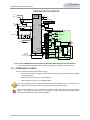
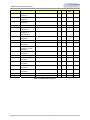
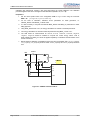
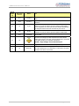
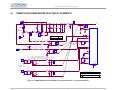
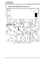
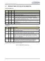
1
71M6531 Demo Board User’s Manual
71M6531 Demo Board
USER’S MANUAL
6/2/2008 5:23:00 PM
v1.5
TERIDIAN Semiconductor Corporation
6440 Oak Canyon Rd., Suite 100
Irvine, CA 92618-5201
Phone: (714) 508-8800 ▪ Fax: (714) 508-8878
http://www.teridian.com/
[email protected]
v1.5
© 2007-2008 TERIDIAN Semiconductor Corporation
Page: 1 of 83
71M6531 Demo Board User’s Manual
Page: 2 of 83
© 2007-2008 TERIDIAN Semiconductor Corporation
v1.5
71M6531 Demo Board User’s Manual
TERIDIAN Semiconductor Corporation makes no warranty for the use of its products, other than expressly contained in the
Company’s warranty detailed in the TERIDIAN Semiconductor Corporation standard Terms and Conditions. The company assumes
no responsibility for any errors which may appear in this document, reserves the right to change devices or specifications detailed
herein at any time without notice and does not make any commitment to update the information contained herein.
v1.5
© 2007-2008 TERIDIAN Semiconductor Corporation
Page: 3 of 83
71M6531 Demo Board User’s Manual
71M6531
Single-Phase Energy Meter IC
DEMO BOARD
USER’S MANUAL
Page: 4 of 83
© 2007-2008 TERIDIAN Semiconductor Corporation
v1.5
71M6531 Demo Board User’s Manual
Table of Contents
1
GETTING STARTED........................................................................................................................................... 9
1.1
General ............................................................................................................................................................... 9
1.2
Safety and ESD Notes ....................................................................................................................................... 9
1.3
Demo Kit Contents ............................................................................................................................................ 9
1.4
Compatibility.................................................................................................................................................... 10
1.5
Suggested Equipment not Included .............................................................................................................. 10
1.6
Demo Board Test Setup .................................................................................................................................. 10
1.6.1
Power Supply Setup ................................................................................................................................... 12
1.6.2
CABLE for Serial Connection ..................................................................................................................... 13
1.6.3
Checking Operation.................................................................................................................................... 13
1.6.4
Serial Connection Setup for the PC............................................................................................................ 14
1.7
Using the Demo Board .................................................................................................................................... 15
1.7.1
Cycling the LCD Display............................................................................................................................. 15
1.7.2
Serial Command Line Interface (CLI) ......................................................................................................... 16
1.7.3
Communicating via Intel Hex Records ....................................................................................................... 22
1.7.4
Using the Battery Modes ............................................................................................................................ 24
1.8
Using the Demo Board for Metering Functions ............................................................................................ 25
1.8.1
Modifying Demo Code to CT or SHUNT Mode ........................................................................................... 25
1.8.2
Using the Demo Board in SHUNT and CT Modes ..................................................................................... 25
1.8.3
Adjusting the kh Factor for the Demo Board .............................................................................................. 26
1.8.4
Adjusting the Demo Boards to Different CT Winding Ratios ...................................................................... 27
1.8.5
Adjusting the Demo Boards to Voltage Transformers or Different Voltage Dividers ................................... 27
1.8.6
Wiring of the Demo Board and a Shunt Resistor ........................................................................................ 27
1.9
Calibration Parameters ................................................................................................................................... 30
1.9.1
General Calibration Procedure ................................................................................................................... 30
1.9.2
Updating the 6531_demo.hex file ............................................................................................................... 30
1.9.3
Calibration Macro File ................................................................................................................................ 31
1.9.4
Updating Calibration Data in EEPROM or Flash ........................................................................................ 31
1.9.5
Loading the 6531_demo.hex file into the Demo Board............................................................................... 31
1.9.6
The Programming Interface of the 71M6531 .............................................................................................. 33
1.10 Demo Code ...................................................................................................................................................... 34
1.10.1 Demo Code Description ............................................................................................................................. 34
1.10.2 Accessing LCD and Sleep Modes from Brownout Mode ............................................................................ 34
1.10.3 Demo Code Memory Locations .................................................................................................................. 34
1.11 Emulator Operation ......................................................................................................................................... 41
2
APPLICATION INFORMATION ........................................................................................................................ 43
2.1
Calibration Theory ........................................................................................................................................... 43
2.1.1
Calibration with Three Measurements ........................................................................................................ 43
2.1.2
Calibration with Five Measurements .......................................................................................................... 45
2.1.3
Fast Calibration .......................................................................................................................................... 46
2.2
Calibration Procedures ................................................................................................................................... 47
2.2.1
General Precautions................................................................................................................................... 47
2.2.2
Calibration Procedure with Three Measurements ...................................................................................... 48
2.2.3
Calibration Procedure with Five Measurements ......................................................................................... 48
2.2.4
Procedure for Auto-Calibration ................................................................................................................... 49
2.2.5
Calibration Spreadsheets ........................................................................................................................... 49
v1.5
© 2007-2008 TERIDIAN Semiconductor Corporation
Page: 5 of 83
71M6531 Demo Board User’s Manual
2.2.6
Compensating for Non-Linearities .............................................................................................................. 51
2.2.7
Calibrating Meters with Combined CT and Shunt Resistor ........................................................................ 51
2.3
Calibrating and Compensating the RTC ........................................................................................................ 54
2.4
Testing the Demo Board ................................................................................................................................. 55
2.4.1
Functional Meter Test................................................................................................................................. 55
2.4.2
EEPROM.................................................................................................................................................... 56
2.4.3
RTC ............................................................................................................................................................ 57
2.4.4
Hardware Watchdog Timer ........................................................................................................................ 57
2.4.5
LCD ............................................................................................................................................................ 57
2.4.6
Supply Current Measurements ................................................................................................................... 58
2.5
TERIDIAN Application Notes .......................................................................................................................... 58
3
HARDWARE DESCRIPTION............................................................................................................................ 59
3.1
Demo Board Description: Jumpers, Switches, Test Points and Connectors ............................................ 59
3.2
Demo Board Hardware Specifications........................................................................................................... 63
4
APPENDIX ........................................................................................................................................................ 65
4.1
71M6531N12A2 Demo Board Electrical Schematic ...................................................................................... 66
4.2
71M6531N12A2 Demo Board Bill of Material................................................................................................. 69
4.3
71M6531N12A2 Demo Board PCB Layout ..................................................................................................... 70
4.4
Debug Board Bill of Material .......................................................................................................................... 75
4.5
Debug Board Schematics ............................................................................................................................... 76
4.6
Debug Board PCB Layout............................................................................................................................... 77
4.7
TERIDIAN 71M6531 Pin-Out Information ....................................................................................................... 80
4.8
Revision History .............................................................................................................................................. 83
List of Figures
Figure 1-1: Demo Board: Basic Connections ............................................................................................................... 10
Figure 1-2: Demo Board: Ribbon Cable Connections .................................................................................................. 11
Figure 1-3: The TERIDIAN 6531 Demo Board with Debug Board Block Diagram (CT Configuration) ......................... 12
Figure 1-4: Port Configuration Setup............................................................................................................................ 14
Figure 1-5: Hyperterminal Sample Window with Disconnect Button ............................................................................ 15
Figure 1-6: Pre-wired shunt resistor ............................................................................................................................. 28
Figure 1-7: Connection of the Pre-Wired Shunt Resistor ............................................................................................. 29
Figure 1-8: Typical Calibration Macro file ..................................................................................................................... 31
Figure 1-9: Emulator Window Showing Reset and Erase Buttons ............................................................................... 32
Figure 1-10: Emulator Window Showing Erased Flash Memory and File Load Menu.................................................. 32
Figure 2-1: Watt Meter with Gain and Phase Errors.................................................................................................... 43
Figure 2-2: Phase Angle Definitions ............................................................................................................................. 47
Figure 2-3: Calibration Spreadsheet for Three Measurements .................................................................................... 49
Figure 2-4: Calibration Spreadsheet for Five Measurements ....................................................................................... 50
Figure 2-5: Calibration Spreadsheet for Fast Calibration ............................................................................................. 50
Figure 2-6: Non-Linearity Caused by Quantification Noise .......................................................................................... 51
Figure 2-7: 71M6531 with Shunt and CT ..................................................................................................................... 52
Figure 2-17: Meter with Calibration System ................................................................................................................. 56
Figure 2-18: Calibration System Screen ...................................................................................................................... 56
Figure 3-1: 71M6531N12A2 Board Connectors, Jumpers, Switches, and Test Points ................................................ 62
Figure 4-1: 71M6531N12A2 Demo Board (REV 2.0): Electrical Schematic 1/3 – Shunt Configuration ....................... 66
Figure 4-2: 71M6531N12A2 Demo Board (REV 2.0): Electrical Schematic 2/3 – CT Configuration ............................ 67
Figure 4-3: 71M6531N12A2 Demo Board (REV 2.0): Electrical Schematic 3/3 – Digital Section ................................ 68
Figure 4-4: 71M6531N12A2 Demo Board: Top Silk Screen ......................................................................................... 70
Page: 6 of 83
© 2007-2008 TERIDIAN Semiconductor Corporation
v1.5
71M6531 Demo Board User’s Manual
Figure 4-5: 71M6531N12A2 Demo Board: Top Copper Layer ..................................................................................... 71
Figure 4-6: 71M6531N12A2 Demo Board: Bottom View with Silk Screen ................................................................... 72
Figure 4-7: 71M6531N12A2 Demo Board: Bottom Copper Layer – Bottom View ........................................................ 73
Figure 4-8: 71M6531N12A2 Demo Board: Bottom Copper Layer – Layer View from Top ........................................... 74
Figure 4-9: Debug Board: Electrical Schematic ........................................................................................................... 76
Figure 4-10: Debug Board: Top View ........................................................................................................................... 77
Figure 4-11: Debug Board: Bottom View...................................................................................................................... 77
Figure 4-12: Debug Board: Top Signal Layer ............................................................................................................... 78
Figure 4-13: Debug Board: Middle Layer 1, Ground Plane .......................................................................................... 78
Figure 4-14: Debug Board: Middle Layer 2, Supply Plane ........................................................................................... 79
Figure 4-15: Debug Board: Bottom Trace Layer .......................................................................................................... 79
Figure 4-16: TERIDIAN 71M6531 LQFP64: Pinout (top view) ..................................................................................... 82
List of Tables
Table 1-1: Jumper settings on Debug Board ................................................................................................................ 13
Table 1-2: Straight cable connections .......................................................................................................................... 13
Table 1-3: Null-modem cable connections ................................................................................................................... 13
Table 1-4: COM Port Setup Parameters ...................................................................................................................... 14
Table 1-5: Selectable Display Options ......................................................................................................................... 16
Table 1-6: Fields of a Hex Record................................................................................................................................ 22
Table 1-7: Data (command) types ................................................................................................................................ 23
Table 1-8: Hex Record examples ................................................................................................................................. 23
Table 1-9: Pre-assembled hex records ........................................................................................................................ 24
Table 1-10: XRAM Locations for Calibration Constants ............................................................................................... 30
Table 1-11: Flash Programming Interface Signals ....................................................................................................... 33
Table 1-12: MPU memory locations ............................................................................................................................. 38
Table 1-13: Values for Pulse Source Registers............................................................................................................ 39
Table 1-14: STATUS register ......................................................................................................................................... 40
Table 1-15: MPU Accumulation Output Variables ........................................................................................................ 41
Table 2-1: Calibration Summary................................................................................................................................... 54
Table 3-1: 71M6531 Demo Board description: 1/3 ....................................................................................................... 59
Table 3-2: 71M6531 Demo Board description: 2/3 ....................................................................................................... 60
Table 3-3: 71M6531 Demo Board description: 3/3 ....................................................................................................... 61
Table 4-1: 71M6531N12A2 Demo Board: Bill of Material (Shunt Version) ................................................................... 69
Table 4-2: Debug Board: Bill of Material ...................................................................................................................... 75
Table 4-3: 71M6531 Pin description 1/2....................................................................................................................... 80
Table 4-4: 71M6531 Pin description 2/2....................................................................................................................... 82
v1.5
© 2007-2008 TERIDIAN Semiconductor Corporation
Page: 7 of 83
71M6531 Demo Board User’s Manual
Page: 8 of 83
© 2007-2008 TERIDIAN Semiconductor Corporation
v1.5
71M6531 Demo Board User’s Manual
1
1
GETTING STARTED
1.1
GENERAL
The TERIDIAN Semiconductor Corporation (TSC) 71M6531 Demo Board is an energy meter IC demonstration board for evaluating the 71M6531D/F device for residential electronic energy metering applications. It
incorporates a 71M6531D/F integrated circuit, peripheral circuitry such as a serial EEPROM, emulator port,
and on-board power supply as well as a companion Debug Board that allows a connection to a PC through
a RS232 port. The Demo Board allows the evaluation of the 71M6531D/F energy meter controller chip for
measurement accuracy and overall system use.
The board is pre-programmed with a Demo Program (file name 6531_demo.hex) in the FLASH memory of
the 71M6531D/F IC. This embedded application is developed to exercise all low-level functions to directly
manage the peripherals and CPU (clock, timing, power savings, etc.).
1.2
SAFETY AND ESD NOTES
Connecting live voltages to the Demo Board system will result in potentially hazardous voltages on the
Demo Board.
EXTREME CAUTION SHOULD BE TAKEN WHEN HANDLING THE DEMO BOARD
ONCE IT IS CONNECTED TO LIVE VOLTAGES!
THE DEMO SYSTEM IS ESD SENSITIVE! ESD PRECAUTIONS SHOULD BE
TAKEN WHEN HANDLING THE DEMO BOARD!
1.3
DEMO KIT CONTENTS
•
•
•
•
•
•
71M6531 Demo Board containing 71M6531D/F IC with preloaded Demo Program and prepared for
either CT or shunt resistor operation
Debug Board
Shunt resistor with wire harness, 400µΩ (for kits shipped in shunt configuration)
Two 5VDC/1,000mA universal wall transformers w/ 2.5mm plug (Switchcraft 712A)
Serial cable, DB9, Male/Female, 2m length (Digi-Key AE1379-ND)
CD-ROM containing documentation (data sheet, board schematics, BOM, layout), Demo Code, and
utilities
Note: The CD-ROM contains a file named readme.txt that specifies all files found on the media and their
purpose.
v1.5
© 2007-2008 TERIDIAN Semiconductor Corporation
Page: 9 of 83
71M6531 Demo Board User’s Manual
1.4
COMPATIBILITY
This manual applies to the following hardware and software revisions:
•
•
•
1.5
71M6531D/F, chip revision A03
Demo Boards D6531N12A2
Demo Board Code revision 6531_4p6q_12may08_0cc.hex, 6531_4p6q_12may08_0sc.hex (EQU 0) ,
6531_4p6q_12may08_1cc.hex EQU 1), 6531_4p6q_12may08_2cc.hex (EQU 2), or later
SUGGESTED EQUIPMENT NOT INCLUDED
For functional demonstration:
•
•
•
•
•
•
PC w/ MS-Windows® versions XP, ME, or 2000, equipped with RS232 port (COM port) via DB9
connector
One or two current transformers (CTs), preferably 2,000:1 turns ratio
For software development (MPU code):
Signum ICE (In Circuit Emulator): ADM-51
http://www.signum.com
Keil 8051 “C” Compiler kit: CA51
http://www.keil.com/c51/ca51kit.htm, http://www.keil.com/product/sales.htm
1.6
DEMO BOARD TEST SETUP
Figure 1-1 shows the basic connections of the Demo Boards plus Debug Boards with the external
equipment.
5VDC Power
Demo
Board
Debug
Board
Spacer
removed
5VDC Power
Host PC
Figure 1-1: Demo Board: Basic Connections
The Debug Board can be plugged into J2 of the Demo Board. One spacer of the Debug Board should be
removed, as shown in Figure 1-1. Alternatively, both boards can be connected using a flat ribbon cable, as
shown in Figure 1-2. A male header has to be soldered to J3 of the Debug Board, and the female-to-female
flat ribbon cable is not supplied with the Demo Kit (use Digi-Key P/N A3AKA-1606M-ND or similar).
Page: 10 of 83
© 2007-2008 TERIDIAN Semiconductor Corporation
v1.5
71M6531 Demo Board User’s Manual
Ribbon Cable
Demo
Board
5VDC Power
5VDC Power
Debug Board
Host PC
Figure 1-2: Demo Board: Ribbon Cable Connections
The 71M6531 Demo Board block diagram is shown in Figure 1-3. It consists of a stand-alone meter Demo
Board and an optional Debug Board. The Demo Board contains all circuits necessary for operation as a
meter, including display, calibration LED, and power supply. The Debug Board, when not sharing a power
supply with the meter, is optically isolated from the meter and interfaces to a PC through a 9 pin serial port.
Connections to the external signals to be measured, i.e. scaled AC voltages and current signals derived
from shunt resistors or current transformers, are provided on the rear side of the Demo Board.
It is recommended to set up the Demo Board with no live AC voltage connected, and to
connect live AC voltages only after the user is familiar with the demo system.
v1.5
© 2007-2008 TERIDIAN Semiconductor Corporation
Page: 11 of 83
71M6531 Demo Board User’s Manual
DEMONSTRATION METER
6531
Single Chip
M eter
DIO6
LOAD A
LOAD B
IB
External Current
Transformers
V3P3
VARh
V3P3
3.3V LCD DISPLAY
IA
IA
VB
DIO7
IB
Wh
VA
V3P3
DIO4
DIO5
EEPROM
ICE Connector
VB
VA
DEBUG BOARD (OPTIONAL)
JP1
1
ISO
MPU HEARTBEAT (5Hz)
V5_DBG
2
ISO
CE HEARTBEAT (1Hz)
V5_DBG
V3P3
NEUTRAL
3.3V
GND
GND
5V DC
3
N/C
TX
10
RX
12
ISO
ISO
GND_DBG
V5_DBG
RTM INTERFACE
GND 5, 7,
9, 11
V3P3D
TMUXOUT
8
CKTEST
6
DB9
to PC
COM Port
RS-232
INTERFACE
ISO
ISO
6
FPGA
DB9
to PC
COM Port
ISO
4
V5_DBG
On-board
components
powered by V3P3D
15, 16
N/C
13, 14
N/C
5V DC
V5_NI
GND_DBG
J2
JP21
4/12/2007
Figure 1-3: The TERIDIAN 6531 Demo Board with Debug Board Block Diagram (CT Configuration)
Note: All analog input signals are referenced to the V3P3A net (3.3V power supply to the chip).
1.6.1 POWER SUPPLY SETUP
There are several choices for meter the power supply:
•
Internal (using the AC line voltage). The internal power supply is only suitable when the line voltage
exceeds 220V RMS.
•
External 5VDC connector (J1) on the Demo Board
•
External 5VDC connector (J1) on the Debug Board.
The power supply jumper, JP1, must be consistent with the power supply choice. JP1 connects the AC
line voltage to the internal power supply. This jumper should usually be left in place.
When the Demo Board is in shunt configuration, the shunt resistor has to be connected as shown in
Figure 1-7 for the board to be powered via J1. Alternatively, a jumper cable between any header labeled
V3P3 and the NEUTRAL terminal (J9) can be supplied.
Page: 12 of 83
© 2007-2008 TERIDIAN Semiconductor Corporation
v1.5
71M6531 Demo Board User’s Manual
1.6.2 CABLE FOR SERIAL CONNECTION
For connection of the DB9 serial port to a PC, either a straight or a so-called “null-modem” cable may be
used. JP1 and JP2 are plugged in for the straight cable, and JP3/JP4 are empty. The jumper configuration is
reversed for the null-modem cable, as shown in Table 1-3.
Jumpers on Debug Board
Cable
Configuration
Mode
JP1
JP2
JP3
JP4
Straight Cable
Default
Installed
Installed
--
--
Null-Modem Cable
Alternative
--
--
Installed
Installed
Table 1-1: Jumper settings on Debug Board
JP1 through JP4 can also be used to alter the connection when the PC is not configured as a DCE device.
Table 1-2 shows the connections necessary for the straight DB9 cable and the pin definitions.
PC Pin
Function
Demo Board Pin
2
TX
2
3
RX
3
5
Signal Ground
5
Table 1-2: Straight cable connections
Table 1-3 shows the connections necessary for the null-modem DB9 cable and the pin definitions.
PC Pin
Function
Demo Board Pin
2
TX
3
3
RX
2
5
Signal Ground
5
Table 1-3: Null-modem cable connections
1.6.3 CHECKING OPERATION
A few seconds after power up, the LCD display on the Demo Board should briefly display the following
welcome text:
H
E
L
L
0
After the “HELLO” text, the LCD should display the following information:
W
h
and:
0.
0
0
1
The text “Wh” indicates that accumulated Watt-hours are displayed. In the case shown above, 0.001 Wh
were accumulated. The display will be cycling from numeric to text, indicating activity of the MPU inside the
71M6531D/F.
In Mission Mode, the display can be cycled to display VARh, PF and other parameters by pressing
the pushbutton (PB).
v1.5
© 2007-2008 TERIDIAN Semiconductor Corporation
Page: 13 of 83
71M6531 Demo Board User’s Manual
1.6.4 SERIAL CONNECTION SETUP FOR THE PC
After connecting the DB9 serial port to a PC, start the HyperTerminal application (or any other suitable
communication program) and create a session using the communication parameters shown in Table 1-4.
Setup Parameter
Value
Port speed (baud)
9600/300g
Data bits
Parity
Stop bits
Flow control
8
none
1
XON/XOFF
g depending on the jumper
setting at JP12
Table 1-4: COM Port Setup Parameters
HyperTerminal can be found by selecting Programs ÆAccessories Æ Communications from the Windows©
start menu. The connection parameters are configured by selecting File Æ Properties and then by pressing
the Configure button (see Figure 1-4).
A setup file (file name “Demo Board Connection.ht”) for HyperTerminal that can be loaded with File Æ Open
is also provided with the tools and utilities on the supplied CD-ROM.
Figure 1-4: Port Configuration Setup
Note: Port parameters can only be adjusted when the connection is not active. The disconnect button, as
shown in Figure 1-5 must be clicked in order to disconnect the port.
Page: 14 of 83
© 2007-2008 TERIDIAN Semiconductor Corporation
v1.5
71M6531 Demo Board User’s Manual
Figure 1-5: Hyperterminal Sample Window with Disconnect Button
1.7
USING THE DEMO BOARD
The 71M6531 Demo Board is a ready-to-use meter prepared for use with an external shunt resistor.
Using the Demo Board involves communicating with the Demo Code. An interactive command line interface
(CLI) is available as part of the Demo Code. The CLI allows modifications to the metering parameters,
access to the EEPROM, initiation of auto-calibration sequences, selection of the displayed parameters,
changing calibration factors and many more operations.
Before evaluating the 71M6531 Demo Board, users should get familiar with the commands and responses
of the CLI. A complete description of the CLI is provided in section 1.7.2.
1.7.1 CYCLING THE LCD DISPLAY
The Demo Codes for the 71M6531 Demo Board allow cycling of the display using the PB button. By briefly
pressing the button, the next available parameter from Table 1-5 is selected. This makes it easy to navigate
various displays for Demo Boards that do not have the CLI.
v1.5
© 2007-2008 TERIDIAN Semiconductor Corporation
Page: 15 of 83
71M6531 Demo Board User’s Manual
Step
Text Display
1
Wh
2
VARh
Accumulated reactive energy [VARh].
3
Hours
Expired hours after power-up or reset
4
Time
Time of day (hh.mm.ss).
5
Date
Date (yyyy.mm.dd).
6
PF
7
Edges
8
Pulses
8
A
RMS current at phase A input [A].
8
V
RMS voltage at the VA_IN input [V].
8
Bat V
8
Delta T
Displayed Parameter
Accumulated real energy [Wh]. The default display setting after power-up
or reset.
Current power factor.
Count of zero crossings in the last accumulation interval.
Number of emitted pulses.
Measured battery voltage [V].
Temperature difference from calibration temperature. Displayed in 0.1°C
Table 1-5: Selectable Display Options
1.7.2 SERIAL COMMAND LINE INTERFACE (CLI)
Once, communication to the Demo Board is established, press <CR> and the Demo Program prompt (“>”)
should appear. Type >i to verify that the Demo Program version is revision 4p6q or later.
Users should familiarize themselves with the Demo Program commands described in the tables below.
The Demo Program (Demo Code) is compiled with EEPROM specified as the non-volatile memory. This
means that the default calibration factors are stored in flash memory while the calibration factors resulting
from an actual calibration are stored in EEPROM.
The tables below describe the commands in detail. Type ‘?’ for a display of available commands.
Page: 16 of 83
© 2007-2008 TERIDIAN Semiconductor Corporation
v1.5
71M6531 Demo Board User’s Manual
Commands for CE Data Access:
]
CE DATA ACCESS
Description:
Usage:
Command
combinations:
Example:
Remarks
Allows user to read from and write to CE data space.
] [Starting CE Data Address] [option]…[option]
]???
Read consecutive 16-bit words in Decimal
]$$$
Read consecutive 16-bit words in Hex
]U
Update default version of CE Data in EEPROM.
Important: The CE must be stopped (CE0)
before issuing this command!
]40$$$
Reads CE data words 0x40, 0x41 and 0x42.
]7E=12345678=9876ABCD
Writes two words starting @ 0x7E
CE data space is the address range from 0x1000 to 0x13FF. All CE data words are in 4-byte (32bit) format. The offset of 0x1000 does not have to be entered when using the ] command, thus
typing ]A? will access the 32-bit word located at the byte address 0x1000 + 4 * A = 0x1028.
Commands for MPU/XDATA Access:
)
MPU DATA ACCESS
Description:
Usage:
Command
combinations:
Example:
Remarks
Allows user to read from and write to MPU data space.
) [Starting MPU Data Address] [option]…[option]
)???
Read three consecutive 32-bit words in Decimal
)$$$
Read three consecutive 32-bit words in Hex
)a=n=m
Write the values n and m to two consecutive
addresses starting at a
)08$$$$
Reads data words 0x08, 0x0C, 0x10, 0x14
)04=12345678=9876ABCD
Writes two words starting @ 0x04
MPU or XDATA space is the address range for the MPU XRAM (0x0000 to 0x0FFF). All MPU data words
are in 4-byte (32-bit) format. Typing ]A? will access the 32-bit word located at the byte address 4 *
A = 0x28. The energy accumulation registers of the Demo Code can be accessed by typing two
question marks (“??”).
v1.5
© 2007-2008 TERIDIAN Semiconductor Corporation
Page: 17 of 83
71M6531 Demo Board User’s Manual
Commands for I/O RAM (Configuration RAM) and SFR Control:
R
DIO AND SFR CONTROL
Description:
Usage:
Remarks
Allows the user to read from and write to I/O RAM and special function registers (SFRs).
R [option] [register] … [option]
Command
combinations:
RIx…
Select I/O RAM location x (0x2000 offset is automatically added)
Rx…
Select internal SFR at address x
Rx???...
Read consecutive SFR registers in decimal
Rx$$$...
Read consecutive registers in hex notation
Example:
RI60$$$$
Read all four RTM probe registers
DIO or Configuration RAM space is the address range 0x2000 to 0x20FF.
registers used for configuring basic hardware and functional properties of the
organized in bytes (8 bits). The 0x2000 offset is automatically added when
typed. The SFRs (special function registers) are located in internal RAM
starting at address 0x80.
This RAM contains
71M6531D/F and is
the command RI is
of the 80515 core,
Commands for EEPROM Control:
EE
EEPROM CONTROL
Description:
Usage:
Remarks
Allows user to enable read and write to EEPROM.
EE [option] [arguments]
Command
combinations:
Example:
EECn
EEPROM Access (1 Æ Enable, 0 Æ Disable)
EERa.b
Read EEPROM at address 'a' for 'b' bytes.
EEE
Erase the EEPROM
EESabc..xyz
Write characters to buffer (sets Write length)
EETa
Transmit buffer to EEPROM at address 'a'.
EEWa.b...z
Write values to buffer
EEShello; EET$0210
Writes 'hello' starting at EEPROM address 0x210.
The EEC1 command must be issued before the EEPROM interface can be used. The execution of the EEE
command takes several seconds. During this time, no other commands can be entered.
Auxiliary Commands:
AUXILIARY
Remarks
Description:
Various
Commands:
,
Typing a comma (“,”) repeats the command issued
from the previous command line. This is very helpful
when examining the value at a certain address over
time, such as the XRAM address for the temperature.
/
The slash (“/”) is useful to separate comments from
commands when sending macro text files via the serial
interface. All characters in a line after the slash are
ignored.
Page: 18 of 83
?
Displays the help menu.
CLC
Enables communication via hex records.
BT
Commands execution of a battery test.
© 2007-2008 TERIDIAN Semiconductor Corporation
v1.5
71M6531 Demo Board User’s Manual
Commands controlling the CE:
C
COMPUTE ENGINE
CONTROL
Description:
Remarks
Allows the user to enable and configure the compute engine.
Usage:
C [option] [argument]
Command
combinations:
Example:
CEn
Compute Engine Enable (1 Æ Enable, 0 Æ Disable)
CTn
Select input n for TMUX output pin. Enter n in hex
notation.
CREn
RTM output control (1 Æ Enable, 0 Æ Disable)
CRSa.b.c.d
Selects CE addresses for RTM output (maximum of
four)
CE0
Disables the CE
CT1E
Selects the CE_BUSY signal for the TMUX output pin
Calibration Commands:
CL
CALIBRATION CONTROL
Remarks
Calibration-related commands. A full auto-calibration can be implemented by compiling the
Demo Code with auto-calibration selected as an option. Due to space restrictions, the
auto-calibration is not implemented in the Demo Code supplied with the Demo Boards.
Description:
Usage:
CL [option]
Command
combinations:
CLC
Loads a calibration via serial port
CLB
Starts an auto-calibration sequence
CLD
Restores calibration to defaults
CLR
Restores calibration from EEPROM
CLS
Saves calibration to EEPROM
Commands for Identification and Information:
I
INFORMATION MESSAGES
Description:
Remarks
Allows user to display information messages.
Usage:
I
Example:
I
Returns the Demo Code version
The I command is used to identify the revisions of Demo Code and the contained CE code.
v1.5
© 2007-2008 TERIDIAN Semiconductor Corporation
Page: 19 of 83
71M6531 Demo Board User’s Manual
Commands for Controlling the Metering Values Shown on the LCD Display:
METER DISPLAY
CONTROL (LCD)
M
Description:
Usage:
Command
combinations:
Remarks
Allows user to select internal variables to be displayed.
M [option]. [option]
M
kWh Total Consumption (display wraps around at 999.999)
M1
Temperature (C° delta from nominal)
M2
Frequency (Hz)
M3. [phase]
kWh Total Consumption (display wraps around at 999.999)
M4. [phase]
kWh Total Inverse Consumption (display wraps around at
999.999)
M5. [phase]
kVARh Total Consumption (display wraps around at 999.999)
M6. [phase]
kVAh Total Inverse Consumption (display wraps around at
999.999)
M7. [phase]
VAh Total (display wraps around at 999.999)
M9
Real Time Clock
M10
Calendar Date
M13. n
Main edge count (n = 0: accumulated, n = 1: last second)
M17
Battery voltage. Display will return to M3 after a few seconds.
Example:
M3.1
Displays Wh total consumption of phase A.
Displays for total consumption wrap around at 999.999kWh (or kVARh, kVAh) due to the
number of available display digits. Internal registers (counters) of the Demo Code are 64 bits
wide and do not wrap around.
The internal accumulators in the Demo Code use 64 bits and will neither overflow nor wrap
around under normal circumstances. The restriction to only six digits is due to the
requirement to provide one digit showing the display mode that is separated by a blank digit
from the displayed values.
Commands for Controlling the RMS Values Shown on the LCD Display:
MR
Description:
Usage:
Command
combinations:
Example:
METER RMS DISPLAY
CONTROL (LCD)
Remarks
Allows user to select meter RMS display for voltage or current.
MR [option]. [option]
MR1. [phase]
Displays instantaneous RMS current
MR2. [phase]
Displays instantaneous RMS voltage
MR1.2
Displays phase b RMS current.
Commands for Controlling the MPU Power Save Mode:
PS
Description:
POWER SAVE MODE
Remarks
Enters power save mode
Disables CE, ADC, CKOUT, ECK, RTM, TMUX VREF,
and serial port, sets MPU clock to 38.4KHz.
Usage:
PS
Return to normal mode is achieved by issuing a hardware reset.
Page: 20 of 83
© 2007-2008 TERIDIAN Semiconductor Corporation
v1.5
71M6531 Demo Board User’s Manual
Commands for Controlling the RTC:
RT
REAL TIME CLOCK
CONTROL
Description:
Usage:
Command
combinations:
Example:
Remarks
Allows the user to read and set the real time clock.
RT [option] [value] … [value]
RTDy.m.d.w: Day of week
(year, month, day, weekday [1 = Sunday]). Weekday is
automatically set if omitted.
RTR
Read Real Time Clock.
RTTh.m.s
Time of day: (hr, min, sec).
RTAs.t
Real Time Adjust: (speed, trim)
RTD05.03.17.5
Programs the RTC to Thursday, 3/17/2005
Reset Commands:
Z, W
Description:
Usage:
RESET
Remarks
Allows the user to cause soft or watchdog resets
Z
Soft reset
W
Simulates watchdog reset
The Z command acts like a hardware reset. The energy accumulators in XRAM will retain their values.
Commands for Controlling the LCD and Sleep Modes (when in Brownout Mode):
B
POWER MODE CONTROL
Description:
Allows the user switch to LCD and Sleep mode when the 71M6531D/F is in Brownout
mode.
Usage:
B [option] [value]
Command
combinations:
BL
Enters LCD mode
BS
Enters Sleep mode
BWSn
Prepares Sleep mode with the wakeup timer set to n
seconds
BWMm
Prepares Sleep mode with the wakeup timer set to m
minutes
BWS8
BS
Enters Sleep mode with the wakeup timer set to 8
seconds. The 71M6531D/F will enter Sleep mode and
return to Brownout mode after 8 seconds.
Example:
v1.5
Remarks
© 2007-2008 TERIDIAN Semiconductor Corporation
Page: 21 of 83
71M6531 Demo Board User’s Manual
Commands for Error Recording:
ER
ERROR RECORDING
Description:
Allows the user display and clear the error log.
Usage:
ER [option] [value]
Command
combinations:
ERC
Clears all errors from error log
ERD
Displays error log
ERS+n
Enters error number n in error log
ERS+10
Enters error number 10 in error log
Example:
Remarks
1.7.3 COMMUNICATING VIA INTEL HEX RECORDS
Communication with the 71M6531D/F IC, especially by computers and/or ATE, may also be accomplished
using a simplified protocol based on Intel Hex records. These records can still be sent and received with an
ordinary terminal, and coding and decoding of commands and responses is straight-forward.
Using the Hex-Record Format
Intel's Hex-record format allows program or data files to be encoded in a printable (ASCII) format, allowing
editing of the object file with standard tools and easy file transfer between a host and target. An individual
hex-record is a single line in a file composed of one or several Hex-records.
Entering “CLC” from the text-based command line interface enables the hex-record interface.
Hex-Records are character strings made of several fields which specify the record type, record length,
memory address, data, and checksum. Each byte of binary data is encoded as a 2-character hexadecimal
number: the first ASCII character representing the high-order 4 bits, and the second the low-order 4 bits of
the byte. The six fields that comprise a Hex-record are defined in Table 1-6.
Field
Name
Characters
Description
1
Start code
1
An ASCII colon (":")
2
Byte count
2
The count of the character pairs in the data field.
3
Address
4
The 2-byte address at which the data field is to be loaded into
memory. This is the physical XRAM or I/O RAM address, not
the 4-byte address used by the command-line interface (CLI).
4
Type
2
5
Data
6
Checksum
0-2n
2
00, 01, or 02.
From 0 to n bytes of executable code, or memory loadable
data.
n is normally 20 hex (32 decimal) or less.
The least significant byte of the two's complement sum of the
values represented by all the pairs of characters in the record
except the start code and checksum.
Table 1-6: Fields of a Hex Record
Each record may be terminated with a CR/LF/NULL character. Accuracy of transmission is ensured by the
byte count and checksum fields. This is important when series of values such as calibration constants are
transmitted to a meter, e.g. by ATE equipment in a factory setting. When entering hex records manually, the
user may also choose “FF” (“wild card”) as the checksum. In this case, the Demo Code omits comparing the
checksum with the received record(s).
This is how the checksum is calculated manually (if necessary):
1) The hex values of all bytes (except start code and checksum itself) are added up.
2) The last two hex digits are subtracted from 0xFF.
3) The value 0x01 is added.
Page: 22 of 83
© 2007-2008 TERIDIAN Semiconductor Corporation
v1.5
71M6531 Demo Board User’s Manual
As opposed to the standardized Hex-records that offer three possible types (data, termination, segment
base), six different types are supported for communicating with the 71M6531D/F. These data types basically
encode command types (read/write) along with the data source or destination, as listed in Table 1-7.
Number
1
Code
00
Function
Write CE data record, contains data and 16-bit CE address (CE data RAM is
located at 0x1000).
2
01
End Of File (Quit) record, a file termination record. Contains no data. This record
has to be the last line of the file, and only one record per file is permitted. The
byte pattern is always ':00000001FF'.
Upon receipt of this record, the Demo Code will transfer the received data into
non-volatile memory (EEPROM).
3
02
Alternate form of Write CE data record (optional). CE data RAM is located at
0x1000.
4
03
Read CE data record, contains empty data field and 16-bit CE address (optional).
CE data RAM is located at 0x1000.
5
04
Write MPU or I/O RAM data record, contains data and 16-bit MPU address.
6
05
Read MPU or I/O RAM data record, contains empty data field and 16-bit MPU
address (optional). I/O RAM is located at 0x2000.
7
06
Write RTC data record, contains data and 16-bit RTC address.
8
07
Read RTC data record, contains empty data field and 16-bit RTC address
(optional).
9
08
Write SFR data record, contains data and 16-bit SFR address (optional). The
MSB is always zero (0).
10
09
Read SFR data record, contains empty data field and 16-bit SFR address
(optional).
Table 1-7: Data (command) types
Table 1-8 lists a few examples of hex records.
Hex Record
:08 0000 06 00 00 0C 03 18 05 06 00 ff
Function
Writes (06) eight bytes (08) to RTC, setting the
RTC to zero seconds (00), minutes (00), 12
hours (0C), Wednesday (03), 24th (18) of May
(05), 2006 (06). Uses the wild card checksum.
:10 0010 00 00004000 00004000 00004000
00004000 E8
Writes the default values (0x4000) for the
calibration constants CAL_IA, CAL_IB,
CAL_VA, and CAL_VC to the XRAM (00),
starting at address 0x10 (0010).
The second command causes the Demo Code
to write the data to permanent storage.
:00 0000 01 FF
:10 1020 03 FF
Causes the Demo Board to display the CE data
from address 0x1020 to 0x102F
Table 1-8: Hex Record examples
The Demo Board will not echo any inputs from the terminal (they screen will stay blank except for
the asterisk (*) issued after the user enters <CR><LF>). It is useful to configure Hyperterminal for
“auto-echo”. This can be done by selecting “Properties” from the “File” menu, then clicking on the
“Settings” tab and clicking the “ASCII Setup” button.
No <ENTER> key is necessary at the end of a manually entered record.
v1.5
© 2007-2008 TERIDIAN Semiconductor Corporation
Page: 23 of 83
71M6531 Demo Board User’s Manual
Spaces in between the fields (to increase readability), as in the example above, are ignored by the Demo
Boards.
If a hex record is accepted, the Demo Board returns a "!". If the hex record is not accepted, the Demo
Board sends a "?" and other text, depending on the context (only the 16KB Demo Code will send text).
When only a partial record is entered, the Demo Board will time out after around 30 seconds and then send
<CR>< LF>.
A number of pre-assembled hex records is supplied with the Demo Code. It is easier to send a pre-assembled record using the “send text file” feature in the “Transfer” menu of Hyperterminal, than assembling hex
record from scratch.
The pre-assembled hex records are contained in a ZIP file named 6531_scripts.zip on the CD-ROM
supplied with the Demo Kits. Table 1-9 shows the records available and their function.
Hex Record Name
set_6531_defaults.txt
Function
Sets the default configuration, including all CE variables. Transferring
this record is necessary when data in the EEPROM is lost or
compromised.
read_6531_temp.txt
Displays the current temperature reading from the CE
set_6531_temp.txt
This record can be edited to set the nominal (calibration) temperature
read_6531_power.txt
Displays the valid power data
read_6531_ce.txt
Displays CE data from memory locations 0x1020 to 0x10FF
read_6531_config.txt
Displays configuration data. This hex record includes comment text
helping to interpret the received data.
set_6531_rtm.txt
Sets up the real-time monitor
Table 1-9: Pre-assembled hex records
1.7.4 USING THE BATTERY MODES
The 71M6531D/F is in so-called Mission mode, as long as 3.3VDC is supplied to the V3P3SYS pin. If this
voltage is below the minimum required operating voltage which is usually indicated by V1 < 1.6 (internal
VBIAS voltage), and if no battery is connected to the VBAT pin, the chip is powered off.
Battery modes can be used if a battery or other DC source supplying a DC voltage with in the operating
limits for the battery input is applied to the battery pin (VBAT, pin 49) of the chip. On the Demo Board, the
battery should be connected to pin 2 (+) and 3 (-) of JP8.
In order to prevent corruption of external memory, which could occur when main power
is removed from the Demo Board while no battery is present, the Demo Code is shipped
with the battery modes DISABLED. When the battery modes are disabled, the MPU will be
halted once it enters brownout mode, even when a battery is present. See section 1.10.2
for instruction on how to enable battery modes.
If the main power source (internal or external power supply) is removed while a battery is connected to JP8
as described above, and if the battery modes are enabled with header JP12, the 71M6531D/F automatically
enters Brownout mode. The Demo Code will then automatically transition from Brownout mode to Sleep
mode.
By pressing the pushbutton PB, the chip is temporarily brought back to LCD mode. After a few seconds in
LCD mode, the chip returns to Sleep mode.
By pressing the RESET pushbutton while the chip is in Sleep mode, the chip will enter Brownout mode.
Both the RESET and PB buttons are powered by the battery voltage (VBAT).
In Brownout mode, the analog functions are disabled, and the MPU functions at very low speed. DIO pins
and the UART are still functional. If the chip supports the command line interface, it will signal Brownout
Page: 24 of 83
© 2007-2008 TERIDIAN Semiconductor Corporation
v1.5
71M6531 Demo Board User’s Manual
mode, and the command prompt “B” will be visible on the terminal connected to the Demo Board, followed
by the “>” sign:
B>
The LCD displays a decimal dot in the left-most digit to indicate that it is in Brownout mode, as shown below:
.
H
E
L
L
O
The following commands can be entered via the CLI in Brownout mode:
•
BL – enters LCD mode
•
BS – enters Sleep mode.
•
BWSn – enters sleep mode for n seconds, then returns to Brownout mode
•
BWMm – enters sleep mode for m minutes, then returns to Brownout mode
In Sleep Mode, almost all functions are disabled. Only the RTC and the wakeup timer are still active. The
wakeup signal from the timer and the pushbutton (SW2 on the Demo Board) take the 71M6531D/F back to
Brownout mode.
A hardware reset, while in any battery mode, takes the 71M6531D/F back to Brownout mode.
1.8
USING THE DEMO BOARD FOR METERING FUNCTIONS
1.8.1 MODIFYING DEMO CODE TO CT OR SHUNT MODE
Script files contained in the CD-ROM shipped with the Demo Kit can be used to modify the constants used
in the Demo Code from CT to shunt mode or vice versa. Three script files are available:
1. 6531ctct.txt sets 6531 Demo Code for IA: 2000:1 CT (Imax
2000:1 CT (ImaxB = 208A)
2. 6531ctshunt.txt: IA: 2000:1 CT (Imax
442A)
= 208A) and IB:
= 208A) IB: 400 μΩ shunt (ImaxB =
3. 6531shuntct.txt: IA: 400 μΩ shunt (Imax
(ImaxB = 208A)
= 442A) IB: 2000:1 CT
To apply a script file, select “transfer -> send_text_file” from the HyperTerminal user interface.
1.8.2 USING THE DEMO BOARD IN SHUNT AND CT MODES
The Demo Board may be used with current shunt sensors of 400µΩ resistance or current transformers
(CTs). It is programmable for a Kh factor of 1.0 and (see Section 0 for adjusting the Demo Board for current
transformers). Section 1.8.6 describes proper wiring and safety precautions for shunt operation.
Once, voltage is applied and load current is flowing, the red LED D5 will flash each time an energy sum of
1.0 Wh is collected. The LCD display will show the accumulated energy in Wh when set to display mode 3
(command >M3 via the serial interface).
Similarly, the red LED D6 will flash each time an energy sum of 1.0 VARh is collected. The LCD display will
show the accumulated energy in VARh when set to display mode 5 (command >M5 via the serial interface).
The D6531N12A2 Demo Boards can be operated with CTs on channel B, which is equipped with the proper
burden resistors for 2000:1 CTs.
v1.5
© 2007-2008 TERIDIAN Semiconductor Corporation
Page: 25 of 83
71M6531 Demo Board User’s Manual
If desired, channel A can be modified for operation with a 2000:1 CT as follows:
1)
2)
3)
Remove R24 and R25. Insert a 1.7Ω resistor each for R24 and for R25.
Connect the output of the CT to terminal J3 on the bottom of the board.
Using the command line interface, change IMAXA to decimal 2080 (>)A=+2080) and WRATE to 1556
(>]21=+1556)
4) Remove R88, install L12 and L9.
Using the command line interface, change IMAXA and WRATE by sending the text file as described in 1.8.1.
Of course, other winding ratios for CTs are possible. Adjusting the board to any CT winding ratio is
described in 1.8.4.
If desired, channel A can be modified for operation with a shunt resistor as follows:
1) Remove R24 and R25. Insert a 10kΩ resistor for R24.
2) Install R88, remove L12 and L9.
3) Connect the shunt resistor wiring harness as shown in Figure 1-7.
Using the command line interface, change IMAXA and WRATE by sending the text file as described in 1.8.1.
1.8.3 ADJUSTING THE KH FACTOR FOR THE DEMO BOARD
The 71M6531 Demo Board is shipped with a pre-programmed scaling factor Kh of 1.0, i.e. 1.0 Wh per pulse.
In order to be used with a calibrated load or a meter calibration system, the board should be connected to
the AC power source using the spade terminals on the bottom of the board. The current transformer or
shunt resistor should be connected to the dual-pin headers on the bottom of the board.
The Kh value can be derived by reading the values for IMAX and VMAX (i.e. the RMS current and voltage
values that correspond to the 250mV maximum input signal to the IC), and inserting them in the following
equation for Kh:
Kh = IMAX * VMAX * 47.1132 / (In_8 * WRATE * NACC * X) = 0.99967 Wh/pulse.
Where IMAX is the current scaling factor, VMAX is the voltage scaling factor, In_8 is the current shunt gain
factor, WRATE is the CE variable controlling Kh, NACC is the product of the I/O RAM registers PRE_SAMPS
and SUM_CYCLES, and X is the pulse frequency factor derived from the CE variables PULSE_SLOW and
PULSE_FAST.
The small deviation between the adjusted Kh of 0.99967 and the ideal Kh of 1.0 is covered by calibration.
The default values used for the 71M6531 Demo Board are:
WRATE:
IMAX:
VMAX:
In_8:
NACC:
X:
826
442
600
1
2520
6
Explanation of factors used in the Kh calculation:
WRATE:
The factor input by the user to determine Kh
IMAX:
The current input scaling factor, i.e. the input current generating 176.8mVrms at the IA, IB,
or IC input pins of the 71M6531D/F. 176.8mV rms is equivalent to 250mV peak.
VMAX:
The voltage input scaling factor, i.e. the voltage generating 176.8mVrms at the VA/VB/VC
input pins of the 71M6531D/F
In_8:
The setting for the additional computational gain (8 or 1) determined by the CE register
IA_SHUNT
NACC:
The number of samples per accumulation interval, i.e. PRE_SAMPS *SUM_CYCLES
X:
The pulse rate control factor determined by the CE registers PULSE_SLOW and
PULSE_FAST
Almost any desired Kh factor can be selected for the Demo Board by resolving the formula for WRATE:
WRATE = (IMAX * VMAX * 47.1132) / (Kh * In_8 * NACC * X)
For the Kh of 1.0Wh, the value 826 (decimal) should be entered for WRATE at location 0x21 (using the CLI
command >]21=+826).
Page: 26 of 83
© 2007-2008 TERIDIAN Semiconductor Corporation
v1.5
71M6531 Demo Board User’s Manual
1.8.4 ADJUSTING THE DEMO BOARDS TO DIFFERENT CT WINDING RATIOS
In general, when IMAX is applied to the primary side of the CT, the voltage Vin at the IA or IB input of the
71M6531D/F IC is determined by the following formula:
Vin = R * I = R * IMAX/N
where N = transformer winding ratio, R = resistor on the secondary side (burden resistor)
If, for example, IMAX = 208A are applied to a CT with a 2500:1 ratio, only 83.2mA will be generated on the
secondary side, causing only 141mV. In this case the Demo Board can be adapted with the steps outlined
below:
Rx =
176.8mV
IMAX
N
1)
The formula
2)
Changing the resistors R24/R25 or R106/R107 to a combined resistance of 2.115Ω (for each pair)
will cause the desired voltage drop of 176.8mV appearing at the IA, or IB inputs of the 71M6531D/F IC.
WRATE should be adjusted to achieve the desired Kh factor, as described in 1.8.3.
3)
is applied to calculate the new resistor Rx. We calculate Rx to 2.115Ω
Simply scaling IMAX is not recommended, since peak voltages at the 71M6531D/F inputs should always be
in the range of 0 through ±250mV (equivalent to 176.8mV rms). If a CT with a much lower winding ratio than
1:2,000 is used, higher secondary currents will result, causing excessive voltages at the 71M6531D/F
inputs. Conversely, CTs with much higher ratio will tend to decrease the useable signal voltage range at the
71M6531D/F inputs and may thus decrease resolution.
1.8.5 ADJUSTING THE DEMO BOARDS TO VOLTAGE TRANSFORMERS OR
DIFFERENT VOLTAGE DIVIDERS
The 71M6531 Demo Board comes equipped with its own network of resistor dividers for voltage
measurement mounted on the PCB. The resistor values result in a ratio of 1:3,393.933. This means that
VMAX equals 276.78mV*3,393.933 = 600V. A large value for VMAX has been selected in order to have
headroom for overvoltages. This choice need not be of concern, since the ADC in the 71M6531D/F has
enough resolution, even when operating at 120Vrms or 240Vrms.
If a different set of voltage dividers or an external voltage transformer is to be used, scaling techniques
similar to those applied for the current transformer should be used.
In the following example we assume that the line voltage is not applied to the resistor divider for VA formed
by R15-R21, R26-R31, and R32, but to a voltage transformer with a ratio N of 20:1, followed by a simple
resistor divider. We also assume that we want to maintain the value for VMAX at 600V to provide headroom
for large voltage excursions.
When applying VMAX at the primary side of the transformer, the secondary voltage Vs is:
Vs = VMAX / N
Vs is scaled by the resistor divider ratio RR. When the input voltage to the voltage channel of the
71M6531D/F is the desired 176.8mV, Vs is then given by:
Vs = RR * 176.8mV
Resolving for RR, we get:
RR = (VMAX / N) / 176.8mV = (600V / 30) / 176.8mV = 170.45
This divider ratio can be implemented, for example, with a combination of one 16.95kΩ and one 100Ω
resistor.
1.8.6 WIRING OF THE DEMO BOARD AND A SHUNT RESISTOR
The 71M6531 Demo Kits are shipped with a pre-wired shunt resistor (400µΩ), as shown in Figure 1-6. This
shunt resistor has to be connected to the 71M6531 Demo Board, as shown in Figure 1-7.
v1.5
© 2007-2008 TERIDIAN Semiconductor Corporation
Page: 27 of 83
71M6531 Demo Board User’s Manual
to IA
reference
to IA_IN
to
LOAD
to meter
power
supply
from
NEUTRAL
Figure 1-6: Pre-wired shunt resistor
Important safety precautions apply when operating the Demo Board in shunt mode:
In shunt configuration, the whole Demo Board will be at line voltage! Touching the board or any
components must be avoided!
It is highly recommended to isolate Demo Board and Debug Board (when used) and to provide
separate power supplies for the Demo Board and Debug Board.
Emulators or other test equipment should never be connected to a live meter without proper
isolation!
Page: 28 of 83
© 2007-2008 TERIDIAN Semiconductor Corporation
v1.5
71M6531 Demo Board User’s Manual
SHUNT
NEUTRAL
Low crosstalk demands
that these current paths
not share a common
wire.
These wires must be
connected directly at
the shunt resistor
RED
BLUE
Power supply and
reference for voltage
measurement
VA_IN
Signal for
current
measurement
Reference for
current
measurement
LIVE
LOAD
WHITE
3 2 1 J3
J4
71M6531
REFA
J9
NEUTRAL
Voltage
Divider
R88
L12 (NC)
C9 1000pF
V3P3
L9 (NC)
R32
750
Ohm
2.5MOhm
R15-R18
C6
R6
Power
Supply
IA
V3P3A
VA
VB
GND
R7
D6531N12A2 Demo Board
10/24/2007
Figure 1-7: Connection of the Pre-Wired Shunt Resistor
While connecting wires to J9 and J4, care should be taken to prevent shorting between LINE
and NEUTRAL.
Before connecting the Demo Board to main power, the resistance between J9 and J4 (LIVE and
NEUTRAL) must be checked! If the resistance is below 100Ω, the wiring must be re-checked!
Only one shunt resistor can be used in a meter, since isolation cannot be maintained when
using more than one shunt resistor.
v1.5
© 2007-2008 TERIDIAN Semiconductor Corporation
Page: 29 of 83
71M6531 Demo Board User’s Manual
1.9
CALIBRATION PARAMETERS
1.9.1 GENERAL CALIBRATION PROCEDURE
Any calibration method can be used with the 71M6531D/F chips. This Demo Board User’s Manual presents
calibration methods with three or five measurements as recommended methods, because they work with
most manual calibration systems based on counting "pulses" (emitted by LEDs on the meter).
Naturally, a meter in mass production will be equipped with special calibration code offering capabilities
beyond those of the Demo Code. It is basically possible to calibrate using voltage and current readings, with
or without pulses involved. For this purpose, the MPU Demo Code can be modified to display averaged
voltage and current values (as opposed to momentary values). Also, automated calibration equipment can
communicate with the Demo Boards via the serial interface and extract voltage and current readings. This is
possible even with the unmodified Demo Code.
A complete calibration procedure is given in section 2.1.3 of this manual.
Regardless of the calibration procedure used, parameters (calibration constants) will result that will have to
be applied to the 71M6531D/F chip in order to make the chip apply the modified gains and phase shifts
necessary for accurate operation. Table 1-10 shows the names of the calibration constants, their function,
and their location in the XRAM.
Again, the command line interface can be used to store the calibration constants in their respective XRAM
addresses. For example, the command
>]11=+16302
stores the decimal value 16302 in the XRAM location controlling the gain of the voltage channel (CAL_VA).
Constant
CE
Address
(hex)
CAL_VA
CAL_VB
0x11
0x13
Adjusts the gain of the voltage channel. +16384 is the
typical value. The gain is directly proportional to the CAL
parameter. Allowed range is 0 to 32767. If the gain is 1%
slow, CAL should be increased by 1%.
CAL_IA
CAL_IB
0x10
0x12
Adjusts the gain of the current channels. +16384 is the
typical value. The gain is directly proportional to the CAL
parameter. Allowed range is 0 to 32767. If the gain is 1%
slow, CAL should be increased by 1%.
PHADJ_A
PHADJ_B
0x18
0x19
This constant controls the CT phase compensation. No
compensation occurs when PHADJ = 0. As PHADJ is
increased, more compensation is introduced.
Note: PHADJ_B 1 applies to 3W/1-phase systems.
Description
Table 1-10: XRAM Locations for Calibration Constants
1.9.2 UPDATING THE 6531_DEMO.HEX FILE
The d_merge program updates the 6531_demo.hex file with the values contained in the macro file. This
program is executed from a DOS command line window. Executing the d_merge program with no
arguments will display the syntax description. To merge macro.txt and old_6531_demo.hex into
new_6531_demo.hex, use the command:
d_merge old_6531_demo.hex macro.txt new_6531_demo.hex
The new hex file can be written to the 71M6531D/F through the ICE port using the ADM51 in-circuit
emulator. This step makes the calibration to the meter permanent.
Page: 30 of 83
© 2007-2008 TERIDIAN Semiconductor Corporation
v1.5
71M6531 Demo Board User’s Manual
1.9.3 CALIBRATION MACRO FILE
The macro file in Figure 1-8 contains a sequence of commands to be used for Demo Boards that provide a
serial command line interface (CLI). It is a simple text file and can be created with Notepad or an equivalent
ASCII editor program. The file is executed with HyperTerminal’s Transfer->Send Text File command.
]10=+16022/
]11=+16381/
]12=+16019/
]13=+16370/
]18=+115/
]19=+113/
ce1
CAL_IA (gain=CAL_IA/16384)
CAL_VA (gain=CAL_VA/16384)
CAL_IB (gain=CAL_IB/16384)
CAL_VB (gain=CAL_VB/16384)
PHADJ_A (default 0)
PHADJ_B (default 0)
Figure 1-8: Typical Calibration Macro file
It is possible to send the calibration macro file to the 71M6531D/F for “temporary” calibration. This will
temporarily change the CE data values. Upon power up, these values are refreshed back to the default
values stored in flash memory. Thus, until the flash memory is updated, the macro file must be loaded each
time the part is powered up. The macro file is run by first issuing the ce0 command to turn off the compute
engine and then sending the file with the transfer Æ send text file procedure. Turning off the CE before
changing CE constants is not a hardware requirement of the chip, but is recommended because of the way
the demo code is written.
Note: Do not use the Transfer Æ Send File command!
1.9.4 UPDATING CALIBRATION DATA IN EEPROM OR FLASH
It is possible to make data permanent that had been entered temporarily into the XRAM. The transfer to
EEPROM is done using the following serial interface command:
>CLS
Thus, after transferring calibration data with manual serial interface commands or with a macro file, all that
has to be done is invoking the CLS command.
It is also possible to write calibration data to flash memory. This is done using the following serial interface
command:
>]U
1.9.5 LOADING THE 6531_DEMO.HEX FILE INTO THE DEMO BOARD
Hardware Interface for Programming: The 71M6531D/F IC provides an interface for loading code into the
internal flash memory. This interface consists of the following signals:
E_RXTX (data), E_TCLK (clock), E_RST (reset), ICE_E (ICE enable)
These signals, along with V3P3D and GND are available on the emulator header J14. Production meters
may be equipped with much simpler programming connectors, e.g. a 6x1 header.
Programming of the flash memory requires a specific in-circuit emulator, the ADM51 by Signum Systems
(http//www.signumsystems.com) or the Flash Programmer (TFP-2) provided by TERIDIAN Semiconductor.
Chips may also be programmed before they are soldered to the board. The TGP1 gang programmer
suitable for high-volume production is available from TERIDIAN.
In-Circuit Emulator: If firmware exists in the 71M6531D/F flash memory, this memory has to be erased
before loading a new file into memory. Figure 1-9 and Figure 1-10 show the emulator software active. In
order to erase the flash memory, the RESET button of the emulator software graphical interface has to be
clicked followed by the ERASE button (Figure 1-9).
Once the flash memory is erased, the new file can be loaded using the commands File followed by Load.
The dialog box shown in Figure 1-10 will then appear making it possible to select the file to be loaded by
clicking the Browse button. Once the file is selected, pressing the OK button will load the file into the flash
memory of the 71M6531D/F IC.
v1.5
© 2007-2008 TERIDIAN Semiconductor Corporation
Page: 31 of 83
71M6531 Demo Board User’s Manual
At this point, the emulator probe (cable) can be removed. Once the 71M6531D/F IC is reset using the reset
button on the Demo Board, the new code starts executing.
Figure 1-9: Emulator Window Showing Reset and Erase Buttons
Figure 1-10: Emulator Window Showing Erased Flash Memory and File Load Menu
Flash Downloader Module (TFP-2): Follow the instructions given in the User Manual for the TFP-2.
Page: 32 of 83
© 2007-2008 TERIDIAN Semiconductor Corporation
v1.5
71M6531 Demo Board User’s Manual
Emulators or other test equipment should never be connected to a live meter without proper
isolation! USB isolators are available from various vendors (see the printed Safety Notice
shipped with the emulator).
1.9.6 THE PROGRAMMING INTERFACE OF THE 71M6531D/F
TFP-2 and ICE Interface Signals
The signals listed in Table 1-11 are necessary for communication between the Flash Programmer or ICE
and the 71M6531D/F.
Direction
Function
Available on
E_TCLK
Output from
71M6531D/F
Data clock
ICE, TFP-2
E_RXTX
Bi-directional
Data input/output
ICE, TFP-2
E_RST
Bi-directional
Flash Downloader Reset
(active low)
ICE, TFP-2
Input of 71M6531D/F
Enables ICE interface
TFP-2
Signal
ICE_ENA
Table 1-11: Flash Programming Interface Signals
The E_RST signal should only be driven by the ICE or Flash Downloader when enabling the ICE interface.
E_RST must be floating at all other times.
The same hardware and software precautions mentioned for emulator (ICE) operation in section
1.11 apply to Flash Programmer operation.
v1.5
© 2007-2008 TERIDIAN Semiconductor Corporation
Page: 33 of 83
71M6531 Demo Board User’s Manual
1.10 DEMO CODE
1.10.1 DEMO CODE DESCRIPTION
The Demo Board is shipped preloaded with Demo Code revision 4p6q or later in the 71M6531D/F chip. The
code revision can easily be verified by entering the command >i via the serial interface (see section 1.7.2).
Check with your local TERIDIAN representative or FAE for the latest revision.
Firmware for the Demo Boards can be updated using either an in-circuit emulator (ICE) or the Flash
Programmer (TFP-2), as described in section 1.9.5.
The Demo Code is useful due to the following features:
•
It provides basic metering functions such as pulse generation, display of accumulated energy,
frequency, date/time, and enables the user to evaluate the parameters of the metering IC such as
accuracy, harmonic performance, etc.
•
It maintains and provides access to basic household functions such as real-time clock (RTC).
•
It provides access to control and display functions via the serial interface, enabling the user to view
and modify a variety of meter parameters such as Kh, calibration coefficients, temperature
compensation etc.
•
It provides libraries for access of low-level IC functions to serve as building blocks for code
development.
The Demo Code source files provided with the TERIDIAN Demo Kits contain numerous routines that are
not implemented. However, by recompiling the code using different compile-time options, many code
variations with different features can be generated. See the Software User’s Guide (SUG) for a complete
description of the Demo Code.
1.10.2 ACCESSING LCD AND SLEEP MODES FROM BROWNOUT MODE
Header JP12 controls the behavior of the Demo Code when system power is off. The setting of JP12 is read
on power up (or after reset), and controls the Demo Code as follows:
•
Jumper across pins 1-2 (GND): The Demo Code will communicate at 9600bd. No transitions to
sleep or LCD mode will be made from brownout mode.
•
Jumper across pins 2-3 (V3P3): The Demo Code will communicate at 300bd. Transitions to sleep
or LCD mode can be made from brownout mode. This operation mode requires connection of a
battery or equivalent DC voltage at JP8.
1.10.3 DEMO CODE MEMORY LOCATIONS
Registers in MPU data RAM can be accessed via the command line interface (CLI) or the using the method
involving Intel Hex records.
Table 1-12 lists MPU addresses of interest. Manipulating the values in the MPU addresses enables the user
to change the behavior of the meter. For example, if the current transformer external to the Demo Board is
changed, a different IMAX value n may have to be applied. This can be done by changing the value in the
address for IMAX using the CLI command )<addess>=n. Modifications to MPU data RAM will not be maintained when a reset or power-up occurs.
Changes to the MPU data RAM can be made permanent by creating a macro file containing
one or several CLI commands and merging the macro file into the code using the d_merge
utility described in section 1.9.2.
The following is an example showing how the battery bit can be set permanently by creating a new object
file:
A text file (battery.txt) is generated, containing the CLI command )1=20. The
using the following syntax (6531_demo.hex is the existing object file):
d_merge utility is called,
d_merge 6531_demo.hex battery.txt new_6531_demo.hex
Now, the object file new_6531_demo.hex contains the battery bit.
Page: 34 of 83
© 2007-2008 TERIDIAN Semiconductor Corporation
v1.5
71M6531 Demo Board User’s Manual
Name
Purpose
Function or LSB Value
IThrshldA
Starting current,
element A
LSB = 216 I 0SQSUM
CLI
F
L in
bits
XDATA
)0
U
32
0x0000
)1
N/A
8
0x0004
0 in this position disables creep
logic for both element A and B.
Config
Configure meter
operation on the fly.
bit 0:** reserved
0: VA = Vrms * Irms;
1:
VA = Wh 2 + VARh2
bit1: 1 = Clears accumulators
bit2:1 = Calibration mode
bit3:** reserved: 1 = enable
tamper detection
bit 5: 1 = battery modes enabled
VPThrshld
error if exceeded.
LSB = 216 V 0SQSUM
)2
U
32
0x0005
IPThrshld
error if exceeded.
LSB = 216 I 0SQSUM
)3
U
32
0x0009
Y_Cal_Deg0
RTC adjust, provided
for optional code.
100ppb
)4
S
16
0x000D
Y_Cal_Deg1
RTC adjust, linear by
temp.
10ppb*ΔT, in 0.1˚C
)5
S
16
0x000F
Y_Cal_Deg2
RTC adjust, squared
by temp.
1ppb*ΔT2, in 0.1˚C
)6
S
16
0x0011
PulseWSource
PulseVSource
Wh Pulse source,
VARh pulse source
selection
See table for PulseWSource and
PulseVSource
)7
U
8
0x0013
Vmax
Scaling Maximum
Voltage for PCB,
equivalent to 176mV
at the VA/VB pins
0.1V
)9
U
16
0x0015
ImaxA
Scaling maximum
current for element
A, equivalent to
176mV at the IA pin
0.1A
)A
U
16
0x0017
ppmc1
ADC linear adjust
with temperature
PPM per degree centigrade
)B
S
16
0x0019
ppmc2
ADC quadratic adjust
with temperature
PPM per degree centigrade
squared
)C
S
16
0x001B
Pulse 3 source
Source for software
pulse output 3
See table for PulseWSource and
PulseVSource
)D
U
8
0x001D
Pulse 4 source
Source for software
pulse output 4
See table for PulseWSource and
PulseVSource
)E
U
8
0x001E
Scal
Duration for autocalibration in
seconds
Count of accumulation intervals to
be used for auto-calibration.
)F
U
16
0x001F
Vcal
Voltage value to be
used for autocalibration
Nominal RMS voltage applied to
all elements during autocalibration (LSB = 0.1V).
)10
U
16
0x0021
v1.5
)8
© 2007-2008 TERIDIAN Semiconductor Corporation
0x0014
Page: 35 of 83
71M6531 Demo Board User’s Manual
Name
Purpose
Function or LSB Value
CLI
For
mat
L in
bits
XDATA
Ical
Current value to be
used for autocalibration
Nominal RMS current applied to
all elements during auto-calibration (LSB = 0.1V). Power factor
must be 1.
)11
U
16
0x0023
VThrshld
Voltage at which to
measure frequency,
zero crossing, etc.
LSB = 216 V 0SQSUM
)12
U
16
0x0025
This feature is approximated using
the CE’s sag detection.)
PulseWidth
Maximum time pulse
is on.
t = (2*PulseWidth + 1)*397µs,
0xFF disables this feature. Takes
effect only at start-up.
)13
S
16
0x0029
TEMP_NOM
Nominal temperature, the temperature
at which calibration
occurs.
Units of TEMP_RAW, from CE. The
value read from the CE must be
entered at this address.
)14
U
32
0x002B
ImaxB
Scaling maximum
current for element
B, equivalent to
176mV at the IA pin
0.1A
)15
U
16
0x002F
IThrshldB
Starting current,
element B
216 I1SQSUM
)16
U
32
0x0031
VBatMin
Minimum battery
voltage.
Same as VBAT, below
)17
U
32
0x0035
CalCount
Count of calibrations
Counts the number of times
calibration is saved, to a maximum
of 255
)18
U
8
0x0039
RTC copy
Nonvolatile copy of
the most recent time
the RTC was read.
Sec, Min, Hr, Day, Date, Month,
Year
)19
)1A
)1B
)1C
)1D
)1E
)1F
U
8
8
8
8
8
8
8
0x017A
0x017B
0x017C
0x017D
0x017E
0x017F
0x0180
deltaT
Difference between
raw temperature and
temp_nom
Same units as TEMP_RAW
)20
S
32
0x003C
Frequency
Frequency
Units from CE.
)21
U
32
0x0040
VBAT*
Last measured
battery voltage
VBAT =
)22
U
32
0x0044
n ADC
29
ADC counts, logically shifted right
by 9 bits. Note: battery voltage is
measured once per day, except
when it is being displayed or
requested with the BT command.
Page: 36 of 83
© 2007-2008 TERIDIAN Semiconductor Corporation
v1.5
71M6531 Demo Board User’s Manual
Name
Purpose
Function or LSB Value
CLI
F
U
L in
bits
32
Vrms_A
Vrms, element A
216 V 0SQSUM
)24
Irms_A
Irms, element A
216 I 0SQSUM
Vrms_B
Vrms, element B
Irms_B
Irms, element B
XDATA
0x004C
)25
U
32
0x0050
216 V1SQSUM
)26
U
32
0x0054
216 I1SQSUM
)27
U
32
0x0058
Vrms_C
(reserved)
)28
U
32
0x005C
Irms_C
(reserved)
)29
U
32
0x0060
STATUS
Status of meter
See table for STATUS register
)2A
U
32
0x0064
CAI
Count of accumulation intervals since
reset, or last clear.
count
)2B
S
32
0x0068
Whi**
Imported Wh, all
elements.
Same LSB as W0SUM
)2C
S
64
0x006C
Whi_A**
Imported Wh,
element A
“
)2E
S
64
0x0074
Whi_B**
Imported Wh,
element B
“
)30
S
64
0x007C
)32
S
64
0x0084
Whi_C**
(reserved)
VARhi*
Imported VARh, all
elements.
LSB of W0SUM
)34
S
64
0x008C
VARhi_A*
Imported VARh,
element A
“
)36
S
64
0x0094
VARhi_B*
Imported VARh,
element B
“
)38
S
64
0x009C
)3A
S
64
0x00A4
VAh**
VAh, all elements.
LSB of W0SUM
)3C
S
64
0x00AC
VAh_A**
VAh, element A
“
)3E
S
64
0x00B4
VAh_B**
VAh, element B
“
)40
S
64
0x00BC
VAh_C**
(reserved)
)42
S
64
0x00C4
VARhi_C*
(reserved)
Whe**
Exported Wh, all
elements.
LSB of W0SUM
)44
S
64
0x00CC
Whe_A**
Exported Wh,
element A
“
)46
S
64
0x00D4
Whe_B**
Exported Wh,
element B
“
)48
S
64
0x00DC
)4A
S
64
0x00E4
Whe_C**
v1.5
(reserved)
© 2007-2008 TERIDIAN Semiconductor Corporation
Page: 37 of 83
71M6531 Demo Board User’s Manual
Name
Purpose
Function or LSB Value
CLI
F
S
L in
bits
64
VARhe
Exported VARh, all
elements.
LSB of W0SUM
)4C
VARhe_A
Exported VARh,
element A
“
VARhe_B
Exported VARh,
element B
0x00EC
)4E
S
64
0x00F4
“
)50
S
64
0x00FC
)52
S
64
0x0104
Whn
Net metered Wh, all
elements A,
LSB of W0SUM
)54
S
64
0x010C
Whn_A
Net metered Wh,
element A, for
autocalibration
LSB of W0SUM
)56
S
64
0x0114
Whn_B
Net metered Wh,
element B
“
)58
S
64
0x011C
)5A
S
64
0x0124
VARhe_C
Whn_C
(reserved)
XDATA
(reserved)
VARhn
Net metered VARh,
all elements
LSB of W0SUM
)5C
S
64
0x012C
VARhn_A
Net metered VARh,
element A, for autocalibration
“
)5E
S
64
0x0134
VARhn_B
Net metered VARh,
element B
“
)60
S
64
0x013C
)62
S
64
0x0144
VARhn_C
(reserved)
MainEdgeCnt
Count of voltage zero
crossings
count
)64
U
32
0x014C
Wh
Default sum of Wh,
nonvolatile
LSB of W0SUM
)65
S
64
0x0150
Wh_A
Wh, element A,
nonvolatile
“
)67
S
64
0x0158
Wh_B
Wh, element B,
nonvolatile
“
)69
S
64
0x0160
Wh_C
(reserved)
)6B
S
64
0x0164
)6D
n/a
32
0x0170
StatusNV
Nonvolatile status
See Status
Table 1-12: MPU memory locations
Page: 38 of 83
© 2007-2008 TERIDIAN Semiconductor Corporation
v1.5
71M6531 Demo Board User’s Manual
Table 1-13 lists the possible entries for the PULSEWSOURCE and PULSEVSOURCE registers.
Decimal Value in
PULSEWSOURCE,
PULSEVSOURCE
Selected Pulse Source
Decimal Value in
PULSEWSOURCE,
PULSEVSOURCE
Selected Pulse Source
0
EQU= 0: W0SUM
if W0SUM > W1SUM, W1SUM
if W1SUM > W0SUM***
18
(reserved)
1
W0SUM
19
WSUM_I
2
W1SUM
20
W0SUM_I
3
(reserved)
21
W1SUM_1
4
VARSUM
22
(reserved)
5
VAR0SUM
23
VARSUM_I
6
VAR1SUM
24
VAR0SUM_I
7
(reserved)
25
VAR1SUM_I
8
I0SQSUM
26
(reserved)
9
I1SQSUM
27
WSUM_E
10
(reserved)
28
W0SUM_E
11
INSQSUM
29
W1SUM_E
12
V0SQSUM
30
(reserved)
13
V1SQSUM
31
VARSUM_E
14
(reserved)
32
VAR0SUM_E
15
VASUM
33
VAR1SUM_E
16
VA0SUM
34
(reserved)
17
VA1SUM
***Changing the equation (EQU) in the I/O RAM does not alter the computations implemented in the
Demo Code.
Table 1-13: Values for Pulse Source Registers
v1.5
© 2007-2008 TERIDIAN Semiconductor Corporation
Page: 39 of 83
71M6531 Demo Board User’s Manual
Table 1-14 explains the bits of the STATUS register.
Bit
Significance
Bit
Significance
0
CREEP: All elements are in creep mode. The pulse
variables will be “jammed” with a constant value on
every accumulation interval to prevent spurious
pulses. Therefore, creep mode stops pulsing even
in internal pulse mode.
16
BATTERY_BAD: The battery voltage is below
VBatMin. The battery is checked only once per
day, right after midnight.
1
--
17
--
2
PB_PRESS: An activation of the pushbutton was
recorded at the most recent reset or wake from
battery mode.
18
CAL_BAD: This bit is set after reset if the
longitudinal checksum over calibration factors is
invalid.
3
WAKE_ALARM: An wake timer flag was recorded
at the most recent wake from battery mode.
19
CLOCK_UNSET: This bit is set after reset if is determined that the RTC has never been set, indicating a bad or non-existent battery.
4
MINVB: Voltage at element B is below VThrshld.
The element is in creep mode.
20
POWER_BAD: This bit is set after reset if is determined that both longitudinal checksums over the
two sets of energy billing data are bad.
5
MAXVA: Voltage at element A is above VThrshldP.
21
GNDNEUTRAL: This bit indicates that a grounded
neutral was detected.
6
MAXVB: Voltage at element B is above VThrshldP.
22
TAMPER: This bit indicates that a tampering
attempt was detected (compilation option, not
supported on standard Demo Board).
7
--
23
VXEDGE: Copy of the CE MAIN_EDGE bit.
8
MINVA: Voltage at element A is below VThrshld.
The element is in creep mode.
24
--
9
WD_DETECT: The most recent reset was caused
by the WDT
25
SAGA: Copy of the CE SAG_A bit w/ a maximum
delay of 8 sample intervals.
10
--
26
SAGB: Copy of the CE SAG_B bit
11
MAXIA: The current in element A is above IThrshld
27
--
12
MAXIB: The current in element B is above IThrshld
28
F0_CE: A copy of the F0 bit of the CE, with a jitter
of up to 8 sample intervals.
13
--
29
--
14
MINT: The temperature is below the minimum (as
defined in option_gbl.h)
30
--
15
MAXT: The temperature is above the maximum (as
defined in option_gbl.h)
31
ONE_SEC: This bit changes every accumulation
interval.
Table 1-14: STATUS register
Page: 40 of 83
© 2007-2008 TERIDIAN Semiconductor Corporation
v1.5
71M6531 Demo Board User’s Manual
MPU ACCUMULATION OUTPUT VARIABLES
Accumulation values are accumulated from XFER cycle to XFER cycle (see Table 1-15). They are
organized as two 32-bit registers. The first register stores the decimal number displayed on the LCD. For
example, if the LCD shows “001.004”, the value in the first register is 1004. This register wraps around after
the value 999999 is reached. The second register holds fractions of the accumulated energy, with an LSB of
9.4045*10-13*VMAX*IMAX*In_8 Wh.
The MPU accumulation registers always hold positive values.
The CLI commands with two question marks, e.g. )39?? should be used to read the variables.
XRAM
Word
Address
0x2C
0x44
0x34
0x4C
0x3C
0x2E
0x46
0x36
0x4E
0x3E
0x30
0x48
0x38
0x50
0x40
Name
Whi
Whe
VARhi
VARhe
VAh
Whi_A
Whe_A
VARhi_A
VARhe_A
VAh_A
Whi_B
Whe_B
VARhi_B
VARhe_B
Vah_B
Description
Total Watt hours consumed (imported)
Total Watt hours generated (exported)
Total VAR hours consumed
Total VAR hours generated (inverse consumed)
Total VA hours
Total Watt hours consumed through element 0
Total Watt hours generated (inverse consumed) through element 0
Total VAR hours consumed through element 0
Total VAR hours generated (inverse consumed) through element 0
Total VA hours in element 0
Total Watt hours consumed through element 1
Total Watt hours generated (inverse consumed) through element 1
Total VAR hours consumed through element 1
Total VAR hours generated (inverse consumed) through element 1
Total VA hours in element 1
Table 1-15: MPU Accumulation Output Variables
1.11 EMULATOR OPERATION
The Signum Systems ADM51 ICE (In-Circuit-Emulator) can be plugged into J14 (or J15) of the Demo Board. The
following conditions are required for successful emulator operation (including code load/erase in flash memory):
1)
2)
Emulator operation is enabled by plugging a jumper into header JP4, pins V3P3D/ICE_E
The CE is disabled (using serial command CE0 or writing 0x00 to I/O RAM cell 0x2000)
For details on code development and test see the Software User’s Guide (SUG).
The emulator can also be operated when the 71M6531D/F is in brownout mode. In brownout mode, the 71M6531D/F
provides power for the pull-up resistors necessary for emulator operation via its V3P3D pin.
Emulators or other test equipment should never be connected to a live meter without proper
isolation! USB isolators are available from various vendors (see the printed Safety Notice
shipped with the emulator).
v1.5
© 2007-2008 TERIDIAN Semiconductor Corporation
Page: 41 of 83
71M6531 Demo Board User’s Manual
Page: 42 of 83
© 2007-2008 TERIDIAN Semiconductor Corporation
v1.5
71M6531 Demo Board User’s Manual
2
2
APPLICATION INFORMATION
2.1
CALIBRATION THEORY
A typical meter has phase and gain errors as shown by φS, AXI, and AXV in Figure 2-1. Following the typical
meter convention of current phase being in the lag direction, the small amount of phase lead in a typical
current sensor is represented as -φS. The errors shown in Figure 2-1 represent the sum of all gain and
phase errors. They include errors in voltage attenuators, current sensors, and in ADC gains. In other
words, no errors are made in the ‘input’ or ‘meter’ boxes.
INPUT
I
φL
φ L is phase lag
ERRORS
−φS
METER
IRMS
A XI
W
Π
V
IDEAL = I ,
φS is phase lead
V RMS
AXV
ERROR ≡
ACTUAL = I AXI
IDEAL = IV cos(φ L )
ACTUAL = IV AXI AXV cos(φ L − φ S )
IDEAL = V ,
ACTUAL = V AXV
ACTUAL − IDEAL ACTUAL
=
−1
IDEAL
IDEAL
Figure 2-1: Watt Meter with Gain and Phase Errors.
During the calibration phase, we measure errors and then introduce correction factors to nullify their effect.
With three unknowns to determine, we must make at least three measurements. If we make more
measurements, we can average the results.
2.1.1 CALIBRATION WITH THREE MEASUREMENTS
A simple calibration method uses three measurements. Typically, a voltage measurement and two Watthour (Wh) measurements are made. A voltage display can be obtained for test purposes via the command
>MR2.1 in the serial interface.
Let’s say the voltage measurement has the error EV and the two Wh measurements have errors E0 and E60,
where E0 is measured with φL = 0 and E60 is measured with φL = 60. These values should be simple ratios—
not percentage values. They should be zero when the meter is accurate and negative when the meter runs
slow. The fundamental frequency is f0. T is equal to 1/fS, where fS is the sample frequency (2560.62Hz). Set
all calibration factors to nominal: CAL_IA = 16384, CAL_VA = 16384, PHADJA = 0.
v1.5
© 2007-2008 TERIDIAN Semiconductor Corporation
Page: 43 of 83
71M6531 Demo Board User’s Manual
From the voltage measurement, we determine that
1.Î
AXV = EV + 1
We use the other two measurements to determine φS and AXI.
IV AXV AXI cos(0 − φ S )
− 1 = AXV AXI cos(φ S ) − 1
IV cos(0)
2.
E0 =
2a.
AXV AXI =
3.
E 60 =
IV AXV AXI cos(60 − φ S )
cos(60 − φ S )
− 1 = AXV AXI
−1
IV cos(60)
cos(60)
3a.
E 60 =
AXV AXI [cos(60) cos(φ S ) + sin(60) sin(φ S )]
−1
cos(60)
E0 + 1
cos(φ S )
= AXV AXI cos(φ S ) + AXV AXI tan(60) sin(φ S ) − 1
Combining 2a and 3a:
4.
E60 = E0 + ( E0 + 1) tan(60) tan(φ S )
5.
tan(φ S ) =
6.Î
φ S = tan −1 ⎜⎜
E 60 − E 0
( E 0 + 1) tan(60)
⎞
E 60 − E 0
⎟⎟
⎝ ( E 0 + 1) tan(60) ⎠
⎛
and from 2a:
7.Î
AXI =
E0 + 1
AXV cos(φ S )
Now that we know the AXV, AXI, and φS errors, we calculate the new calibration voltage gain coefficient from
the previous ones:
CAL _ V NEW =
CAL _ V
AXV
We calculate PHADJ from φS, the desired phase lag:
[
]
⎡
⎤
tan(φ S ) 1 + (1 − 2 −9 ) 2 − 2(1 − 2 −9 ) cos(2πf 0T )
PHADJ = 2 ⎢
⎥
−9
−9
⎣ (1 − 2 ) sin( 2πf 0T ) − tan(φ S ) 1 − (1 − 2 ) cos(2πf 0T ) ⎦
20
Page: 44 of 83
[
© 2007-2008 TERIDIAN Semiconductor Corporation
]
v1.5
71M6531 Demo Board User’s Manual
And we calculate the new calibration current gain coefficient, including compensation for a slight gain
increase in the phase calibration circuit.
CAL _ I
AXI
CAL _ I NEW =
1
1+
2 − 20 PHADJ (2 + 2 −20 PHADJ − 2(1 − 2 −9 ) cos(2πf 0T ))
1 − 2(1 − 2 −9 ) cos(2πf 0T ) + (1 − 2 −9 ) 2
2.1.2 CALIBRATION WITH FIVE MEASUREMENTS
The five measurement method provides more orthogonality between the gain and phase error derivations.
This method involves measuring EV, E0, E180, E60, and E300. Again, set all calibration factors to nominal, i.e.
CAL_IA = 16384, CAL_VA = 16384, PHADJA = 0.
First, calculate AXV from EV:
1.Î
AXV = EV + 1
Calculate AXI from E0 and E180:
IV AXV AXI cos(0 − φ S )
− 1 = AXV AXI cos(φ S ) − 1
IV cos(0)
2.
E0 =
3.
E180 =
4.
E0 + E180 = 2 AXV AXI cos(φ S ) − 2
5.
AXV AXI =
6.Î
AXI =
IV AXV AXI cos(180 − φ S )
− 1 = AXV AXI cos(φ S ) − 1
IV cos(180)
E 0 + E180 + 2
2 cos(φ S )
( E 0 + E180 ) 2 + 1
AXV cos(φ S )
Use above results along with E60 and E300 to calculate φS.
7.
E 60 =
IV AXV AXI cos(60 − φ S )
−1
IV cos(60)
= AXV AXI cos(φ S ) + AXV AXI tan(60) sin(φ S ) − 1
8.
E300 =
IV AXV AXI cos(−60 − φ S )
−1
IV cos(−60)
= AXV AXI cos(φ S ) − AXV AXI tan(60) sin(φ S ) − 1
Subtract 8 from 7
9.
E60 − E300 = 2 AXV AXI tan(60) sin(φ S )
use equation 5:
10.
v1.5
E 60 − E300 =
E 0 + E180 + 2
tan(60) sin(φ S )
cos(φ S )
© 2007-2008 TERIDIAN Semiconductor Corporation
Page: 45 of 83
71M6531 Demo Board User’s Manual
11.
E60 − E300 = ( E0 + E180 + 2) tan(60) tan(φ S )
12.Î
φ S = tan −1 ⎜⎜
⎞
( E 60 − E300 )
⎟⎟
tan(
60
)(
E
E
2
)
+
+
0
180
⎠
⎝
⎛
Now that we know the AXV, AXI, and φS errors, we calculate the new calibration voltage gain coefficient from
the previous ones:
CAL _ V NEW =
CAL _ V
AXV
We calculate PHADJ from φS, the desired phase lag:
[
]
⎡
⎤
tan(φ S ) 1 + (1 − 2 −9 ) 2 − 2(1 − 2 −9 ) cos(2πf 0T )
PHADJ = 2 20 ⎢
⎥
−9
−9
⎣ (1 − 2 ) sin( 2πf 0T ) − tan(φ S ) 1 − (1 − 2 ) cos(2πf 0T ) ⎦
[
]
And we calculate the new calibration current gain coefficient, including compensation for a slight gain
increase in the phase calibration circuit.
CAL _ I NEW =
CAL _ I
AXI
1
1+
2
− 20
PHADJ (2 + 2 PHADJ − 2(1 − 2 −9 ) cos(2πf 0T ))
1 − 2(1 − 2 −9 ) cos(2πf 0T ) + (1 − 2 −9 ) 2
− 20
2.1.3 FAST CALIBRATION
The calibration methods described so far require that the calibration system sequentially applies currents at
various phase angles. A simpler approach is based on the calibration system applying a constant voltage
and current at exactly zero degrees phase angle. This approach also requires much simpler mathematical
operations.
Before starting the calibration process, the voltage and current calibration factors are set to unity (16384)
and the phase compensation factors are set to zero.
During the calibration process, the meter measures for a given constant time, usually 30 seconds, and is
then examined for its accumulated Wh and VARh energy values. Access to the internal accumulation
registers is necessary for this method of calibration. The phase angle introduced by the voltage and/or
current sensors is then simply determined by:
ϕ = a tan
VARh
Wh
CAL_VA is determined by comparing the applied voltage to the measured voltage, or:
CAL _ VA = 16384 ⋅
Page: 46 of 83
Vapplied
Vmeasured
© 2007-2008 TERIDIAN Semiconductor Corporation
v1.5
71M6531 Demo Board User’s Manual
CAL_IA is determined by comparing applied real energy with the measured apparent energy (and
compensating for the change applied to CAL_VA):
CAL _ IA =
16384 ⋅ Whapplied
VAhmeasured ⋅ CAL _ VA
⋅
The derivation of these formulae is shown in the Appendix.
2.2
CALIBRATION PROCEDURES
2.2.1 GENERAL PRECAUTIONS
Calibration requires that a calibration system is used, i.e. equipment that applies accurate voltage, load
current and load angle to the unit being calibrated, while measuring the response from the unit being
calibrated in a repeatable way. By repeatable we mean that the calibration system is synchronized to the
meter being calibrated. Best results are achieved when the first pulse from the meter opens the
measurement window of the calibration system. This mode of operation is opposed to a calibrator that
opens the measurement window at random time and that therefore may or may not catch certain pulses
emitted by the meter.
Note: It is essential for a valid meter calibration to have the voltage stabilized a few seconds before
the current is applied. This enables the Demo Code to initialize the 71M6531D/F and to stabilize the
PLLs and filters in the CE. This method of operation is consistent with meter applications in the field
as well as with metering standards.
Each meter phase must be calibrated individually. The procedures below show how to calibrate a meter
phase with either three or five measurements. The PHADJ equations apply only when a current transformer
is used for the phase in question. Note that positive load angles correspond to lagging current (see Figure
2-2).
Voltage
Positive
direction
Current lags
voltage
(inductive)
+60°
Current
-60°
Current leads
voltage
(capacitive)
Voltage
Generating Energy
Using Energy
Figure 2-2: Phase Angle Definitions
The calibration procedures described below should be followed after interfacing the voltage and current
sensors to the 71M6531D/F chip. When properly interfaced, the V3P3 power supply is connected to the
meter neutral and is the DC reference for each input. Each voltage and current waveform, as seen by the
71M6531D/F, is scaled to be less than 250mV (peak).
v1.5
© 2007-2008 TERIDIAN Semiconductor Corporation
Page: 47 of 83
71M6531 Demo Board User’s Manual
2.2.2 CALIBRATION PROCEDURE WITH THREE MEASUREMENTS
The calibration procedure is as follows:
1.
All calibration factors are reset to their default values, i.e. CAL_IA = CAL_VA = 16384, and PHADJ_A =
0.
2.
An RMS voltage Videal consistent with the meter’s nominal voltage is applied, and the RMS reading
Vactual of the meter is recorded. The voltage reading error Axv is determined as
Axv = (Vactual - Videal ) / Videal
3.
Apply the nominal load current at phase angles 0° and 60°, measure the Wh energy and record the
errors E0 AND E60.
4.
Calculate the new calibration factors CAL_IA, CAL_VA, and PHADJ_A, using the formulae presented in
section 2.1.1 or using the spreadsheet presented in section 2.2.4.
5.
Apply the new calibration factors CAL_IA, CAL_VA, and PHADJ_A to the meter. The memory locations
for these factors are given in section 1.9.1.
6.
Test the meter at nominal current and, if desired, at lower and higher currents and various phase
angles to confirm the desired accuracy.
7.
Store the new calibration factors CAL_IA, CAL_VA, and PHADJ_A in the EEPROM of the meter. If a
Demo Board is calibrated, the methods shown in section 1.9.2 can be used.
2.2.3 CALIBRATION PROCEDURE WITH FIVE MEASUREMENTS
The calibration procedure is as follows:
1)
All calibration factors are reset to their default values, i.e. CAL_IA = CAL_VA = 16384, and PHADJ_A =
0.
2)
An RMS voltage Videal consistent with the meter’s nominal voltage is applied, and the RMS reading
Vactual of the meter is recorded. The voltage reading error Axv is determined as
Axv = (Vactual - Videal ) / Videal
3)
Apply the nominal load current at phase angles 0°, 60°, 180° and –60° (-300°). Measure the Wh energy
each time and record the errors E0, E60, E180, and E300.
4)
Calculate the new calibration factors CAL_IA, CAL_VA, and PHADJ_A, using the formulae presented in
section 2.1.2 or using the spreadsheet presented in section 2.2.4.
5)
Apply the new calibration factors CAL_IA, CAL_VA, and PHADJ_A to the meter. The memory locations
for these factors are given in section 1.9.1.
6)
Test the meter at nominal current and, if desired, at lower and higher currents and various phase
angles to confirm the desired accuracy.
7)
Store the new calibration factors CAL_IA, CAL_VA, and PHADJ_A in the EEPROM of the meter. If the
calibration is performed on a TERIDIAN Demo Board, the methods shown in sections 1.9.2 can be
used.
Page: 48 of 83
© 2007-2008 TERIDIAN Semiconductor Corporation
v1.5
71M6531 Demo Board User’s Manual
2.2.4 PROCEDURE FOR AUTO-CALIBRATION
The fast calibration procedure is supported by the Demo Code when the Auto-Cal function is executed. This
procedure requires the following steps:
1)
Establish load voltage and current from the calibration system. The load angle must be exactly 0.00
degrees.
2)
Enter the expected voltage and current using CLI commands. For example, to calibrate for 240V, 30A
for two seconds, enter )F=2=+2400=+300.
3)
Issue the CLI command CLB.
4)
Wait the specified number of seconds.
5)
Check the calibration factors established by the automatic procedure.
2.2.5 CALIBRATION SPREADSHEETS
Calibration spreadsheets are available from TERIDIAN Semiconductor. They are also included in the CDROM shipped with any Demo Kit. Figure 2-3 shows the spreadsheet for three measurements with three
phases in use (only one phase needs to be used for the 71M6531D/F chip).
Figure 2-3 shows the spreadsheet for five measurements with three phases (only one phase needs to be
used for the 71M6531D/F chip).
71M6511/71M6513/71M6515 Calibration Worksheet
Three Measurements
Enter values in yellow fields
Results will show in green fields…
AC frequency:
50
REV
Date:
4.7
11/18/2005
[Hz]
(click on yellow field to select from pull-down list)
PHASE A
Energy reading at 0°
Energy reading at +60°
Voltage error at 0°
%
-3.846
-3.642
-1.65
Expected voltage
Measured voltage
240
236.04
PHASE B
Energy reading at 0°
Energy reading at +60°
Voltage error at 0°
%
10
10
10
Expected voltage
Measured voltage
240
264
PHASE C
Energy reading at 0°
Energy reading at +60°
Voltage error at 0°
%
-3.8
-9
-3.8
Expected voltage
Measured voltage
240
230.88
fraction
-0.03846
-0.03642
-0.0165
CAL_IA
CAL_VA
PHADJ_A
old
new
16384
16384
16756
16659
220
Voltage
[V]
[V]
fraction
0.1
0.1
0.1
old
CAL_IB
CAL_VB
PHADJ_B
16384
16384
CAL_IC
CAL_VC
PHADJ_C
16384
16384
Positive
direction
new
16384
14895
0
old
new
16409
17031
-5597
+60°
Current
-60°
Current leads
voltage
(capacitive)
[V]
[V]
fraction
-0.038
-0.09
-0.038
Current lags
voltage
(inductive)
Voltage
Generating Energy
Using Energy
Readings: Enter 0 if the error is 0%,
[V]
[V]
enter -3 if meter runs 3% slow.
Figure 2-3: Calibration Spreadsheet for Three Measurements
v1.5
© 2007-2008 TERIDIAN Semiconductor Corporation
Page: 49 of 83
71M6531 Demo Board User’s Manual
71M6511/71M6513/71M6515 Calibration Worksheet
Five Measurements
Results will show in green fields…
Enter values in yellow fields!
PI
REV
Date:
Ts
60
AC frequency:
4.7
10/25/2005
[Hz]
(click on yellow field to select from pull-down list)
PHASE A
Energy reading at 0°
Energy reading at +60°
Energy reading at -60°
Energy reading at 180°
Voltage error at 0°
Expected voltage [V]
PHASE B
Energy reading at 0°
Energy reading at +60°
Energy reading at -60°
Energy reading at 180°
Voltage error at 0°
Expected voltage [V]
PHASE C
Energy reading at 0°
Energy reading at +60°
Energy reading at -60°
Energy reading at 180°
Voltage error at 0°
Expected voltage [V]
%
0
0
0
0
0
fraction
0
CAL_IA
0
CAL_VA
0
PHADJ_A
0
0
240
240
%
0
0
0
0
0
240
%
0
0
0
0
0
Voltage
Current lags
voltage
(inductive)
Positive
direction
old
new
16384
16384
16384
16384
0
+60°
240
Current
-60°
Current leads
voltage
(capacitive)
Voltage
Measured voltage [V]
fraction
0
CAL_IC
0
CAL_VC
0
PHADJ_C
0
0
240
new
16384
16384
0
Measured voltage [V]
fraction
0
CAL_IB
0
CAL_VB
0
PHADJ_B
0
0
240
old
16384
16384
old
new
16384
16384
16384
16384
0
Generating Energy
Using Energy
Readings: Enter 0 if the error is 0%,
enter +5 if meter runs 5% fast,
enter -3 if meter runs 3% slow.
Measured voltage [V]
Figure 2-4: Calibration Spreadsheet for Five Measurements
6521 Fast Calibration Work Sheet
REV
Inputs
Meter
Constants
SUM_CYCLES
60
Current [A]
0.408
Fs
2520.6154
PRE_SUM
42
Voltage [V]
223.4
Wh_A LSB
8.3556E-08
2. CE1 -- Enable CE, wait 2 seconds
VMAX
600
f [Hz]
60
VRMS LSB
4.49525E-07
3. )1=2 -- Clear accumulators, wait 30 seconds
4. CE0 -- Disable CE
IMAX_A
208
CE LSB
6.6952E-13
IMAX_B
208
Wh_B LSB
8.3556E-08
4.8
Procedure:
1. Turn on excitation. Load angle must be exactly 0.00 degrees
5. )2E? -- number of accumulation intervals, enter in spreadsheet
6. )14? -- get VRMS value, enter in spreadsheet
CAI -- )28
Phase A
Phase B
31
31
7. )39???????? )43???????? -- enter accumulated values in spreadsheet
8. ]54? -- get TEMP_RAW_X from CE, write to TEMP_NOM
If not starting w/ fresh calibration factors, enter value of current factors
VRMS -- )23
in column "Old".
Vrms A
Digital
496461520
Enter values in yellow fields!
VRMS
223.17
Results will show in green fields.
Phase A net Wh
)54
)55
0
10070303
Phase A net VARh
Total Wh
0.8414
)5A
)5B
Expected Wh
0.7847
0
84156
0.0070
Total VARh
Phase B net Wh
)56
)57
0
9504914
Old
New
CAL_VA
16384
16401
]9
Angle
CAL_IA
16384
15263
]8
0.4788
PHADJ_A
0
-1312
]C
Angle
0
0.47869219
16384
0
16170
-1973
0
0.72010832
Phase B VARh
Total Wh
0.7942
Expected Wh
0.7847
CAL_IB
PHADJ_B
)47
)48
0
119446
Angle
0.0100
0.7200
Total VARh
Angle
Figure 2-5: Calibration Spreadsheet for Fast Calibration
Page: 50 of 83
© 2007-2008 TERIDIAN Semiconductor Corporation
v1.5
]A
]D
71M6531 Demo Board User’s Manual
2.2.6 COMPENSATING FOR NON-LINEARITIES
Nonlinearity is most noticeable at low currents, as shown in Figure 2-6, and can result from input noise and
truncation. Nonlinearities can be eliminated using the QUANT variable.
12
error [%]
10
error
8
6
4
2
0
0.1
1
10
100
I [A]
Figure 2-6: Non-Linearity Caused by Quantification Noise
The error can be seen as the presence of a virtual constant noise current. While 10mA hardly contribute any
error at currents of 10A and above, the noise becomes dominant at small currents.
The value to be used for QUANT can be determined by the following formula:
error
V ⋅I
100
QUANT = −
VMAX ⋅ IMAX ⋅ LSB
Where error = observed error at a given voltage (V) and current (I),
VMAX = voltage scaling factor, as described in section 1.8.3,
IMAX = current scaling factor, as described in section 1.8.3,
LSB = QUANT LSB value = 7.4162*10-10W
Example: Assuming an observed error as in Figure 2-6, we determine the error at 1A to be +1%. If VMAX is
600V and IMAX = 208A, and if the measurement was taken at 240V, we determine QUANT as follows:
1
240 ⋅ 1
100
QUANT = −
= −11339
600 ⋅ 208 ⋅ 7.4162 ⋅ 10 −10
QUANT is to be written to the CE location 0x2F. It does not matter which current value is chosen as long as
the corresponding error value is significant (5% error at 0.2A used in the above equation will produce the
same result for QUANT).
Input noise and truncation can cause similar errors in the VAR calculation that can be eliminated using the
QUANT_VAR variable. QUANT_VAR is determined using the same formula as QUANT.
2.2.7 CALIBRATING METERS WITH COMBINED CT AND SHUNT RESISTOR
In many cases it is desirable to discourage tampering by using two current sensors. The simple tampering
method that involves connecting the low side of the load to earth ground (neutral) can be detected by adding
a second current sensor in the neutral path, as shown in Figure 2-7.
In this configuration, the shunt resistor is connected to the IA channel while the current transformer is
connected to the IB channel of the 71M6531D/F.
v1.5
© 2007-2008 TERIDIAN Semiconductor Corporation
Page: 51 of 83
71M6531 Demo Board User’s Manual
Calibrating this arrangement requires a few extra steps above the regular calibration. The calibration
procedure applies to the sensor arrangement described above (SHUNT = IA, CT = IB).
Preparation:
1.
Set the meter equation field of the configuration RAM for EQU to zero using the command:
RI00 = 10 (i.e. EQU = 0; CE_EN =1; TMUX = 0)
2.
For the sake of calculation, individual WRATE parameters for Pulse generation, i.e.
WRATE_SHUNT and WRATE_CT will be used.
3.
It is also necessary to compute and estimate IMAX_SHUNT and IMAX_CT parameters for meter
billing purposes.
4.
Using IMAX_SHUNT and VMAX, the energy calculations for channel A should be performed.
5.
The energy calculations for channel B should be performed using IMAX_CT and VMAX.
6.
The LSB values for measurements for W0SUM, W1SUM, VAR0SUM, VAR1SUM, I0SQSUM,
I1SQSUM, V0SQSUM should be modified to compute the correct energy values. That is,
IMAX_SHUNT and IMAX_CT should be applied separately to individual channels based on the
sensor connections.
7.
Before starting a calibration, all calibration factors must be in their default state, i.e. CAL_IA (0x10),
CAL_VA (0x11), CAL_IB (0x12) must be 16384. PHADJ_A (0x18) and PHADJ_B (0x19) should be
zero.
LIVE
NEUT
SHUNT
CT
LOAD
71M6531
71M6511
IB
IA
VA
V3P3
Figure 2-7: 71M6531 with Shunt and CT
Page: 52 of 83
© 2007-2008 TERIDIAN Semiconductor Corporation
v1.5
71M6531 Demo Board User’s Manual
Calibrating for Shunt Resistor (Channel A):
1.
Calculate IMAX for the shunt resistor (IMAX_SHUNT). This can be done by using the following
formula:
IMAX_SHUNT = ViMAX/RSH
The ViMAX value is the maximum analog input voltage for the channel, typically 176.8mV (RMS),
and RSH is the resistance value of the shunt resistor.
The value obtained for IMAX_SHUNT is stored at the MPU address 0x0A, using the command
)A= IMAX_SHUNT of the Demo Code supplied by TERIDIAN.
2.
Compute WRATE_SHUNT based on IMAX_SHUNT and VMAX and the formula given in 1.8.3:
WRATE_SHUNT = (IMAX_SHUNT * VMAX * 47.1132) / (Kh * In_8 * NACC * X)
Use VMAX = 600V (RMS) for the 6531 Demo Board if the resistor divider for VA has not been
changed.
3.
Update the WRATE register (at CE address 0x2D) with WRATE_SHUNT, using the command
]21= WRATE_SHUNT.
4.
Test for accuracy at 15A, 240V at phase angle 0, phase angle 60° and at phase angle –60°.
5.
Apply the error values to the calibration spreadsheet (revision 2.0 or later) and determine the
calibration factors for channel A, i.e. CAL_IA, CAL_VA, and PHADJ_A.
6.
Update the CE registers 0x08, 0x09 and 0x0E of the compute engine with the calibration factors
obtained from the spreadsheet, using the commands ]10=CAL_IA, ]11=CALVA, and
]18=PHADJ_A.
7.
Retest for accuracy at several currents and phase angles.
At this point, channel A is calibrated. WSUM will be based on the voltage applied to the meter and the
current flowing through the shunt resistor. The pulses generated will be based on the parameters entered for
channel A.
Calibration for CT (Channel B):
1.
Compute IMAX for the CT channel (IMAX_CT), based on the CT turns ratio N and the termination
resistor value RT using the formula:
IMAX_CT = 176.8mV* N / RT
This value is used in the following step as IMAX_CT.
2.
Compute WRATE_CT based on the values obtained for IMAX_CT and the formula given in 1.8.3:
WRATE_CT = (IMAX_CT * VMAX * 47.1132) / (Kh * In_8 * NACC * X)
3.
Update the WRATE register (CE address 0x2D) with WRATE_CT, using the command
]21= WRATE_CT.
4.
Enter the command >)7=2. Configure W1SUM as external pulse source since the CT is connected
to channel 1 for VA*IB.
5.
Test for accuracy at 15A, 240V at phase angle 0, phase angle 60° and at phase angle –60°.
6.
Apply these values to the calibration spread sheet (revision 2.0 or later) and derive the calibration
factor PHADJ_B.
7.
Update only the CE address 0x0F with the value for PHADJ_B using the command ]19=
PHADJ_B.
8.
Adjust CAL_IB for the total error found in the accuracy test using the formula
CAL_IB = 16384 * (1 - error/100)
v1.5
© 2007-2008 TERIDIAN Semiconductor Corporation
Page: 53 of 83
71M6531 Demo Board User’s Manual
That is, if the chip reports an error of -2.5%, CAL_IB should be adjusted to a value of
(16384 * (1 - (-2.5/100)).
9.
Since CAL_VA and CAL_IA have already been adjusted for channel A, these registers should not
be updated.
10. Retest for accuracy at several currents and phase angles.
After completing the calibration, the energy values W0SUM, based on VA*IA and W1SUM, based on VA*IB
are accessible to the MPU firmware. The pulse rate is controlled by W1SUM and determined by the
parameters selected for the CT channel (VA, IB). Differences between W0SUM and W1SUM, indicating
tampering, can be detected by the MPU for each accumulation interval.
Note: The user has to customize the Demo Code to utilize the values obtained from the VA, IA, and
IB channels for proper calculation of tariffs.
Table 2-1 summarizes the important parameters used in the calibration procedure.
Channel
Sensor
Formula
Parameters
W Pulse
Generation
VAR Pulse
Generation
A
Shunt
Resistor
WASUM = VA*IA
VARASUM = VA*IA
VMAX = VMAX
IMAX = IMAX_SHUNT
WRATE = WRATE_SHUNT
WASUM
VARASUM
B
CT
WBSUM = VA*IB
VARBSUM = VA*IB
VMAX = VMAX
IMAX = IMAX_CT
WRATE = WRATE_CT
WBSUM
VARBSUM
Table 2-1: Calibration Summary
2.3 CALIBRATING AND COMPENSATING THE RTC
The real-time clock (RTC) of the 71M6534 is controlled by the crystal oscillator and thus only as accurate as
the oscillator. The 71M6534 has two rate adjustment mechanisms:
•
Analog rate adjustment, using the I/O RAM register RTCA_ADJ[6:0]. This adjustment is used to set
the oscillator frequency at room temperature close to the target (ideal) value. Adjusting
RTCA_ADJ[6:0] will change the time base used for energy measurements and thus slightly
influence these energy measurements. Therefore it is recommended to adjust the RTC before
calibrating a meter.
•
Digital rate adjustment is used to dynamically correct the oscillator rate under MPU control. This is
necessary when the IC is at temperatures other than room temperature to correct for frequency
deviations.
The analog rate adjustment uses the I/O RAM register RTCA_ADJ[6:0], which trims the crystal load capacitance. Setting RTCA_ADJ[6:0] to 00 minimizes the load capacitance, maximizing the oscillator frequency.
Setting RTCA_ADJ[6:0] to 3F maximizes the load capacitance, minimizing the oscillator frequency.
The maximum adjustment is approximately ±60ppm. The precise amount of adjustment will depend on the
crystal and on the PCB properties. The adjustment may occur at any time, and the resulting clock frequency
can be measured over a one-second interval using a frequency counter connected to the TMUXOUT pin,
while 0x10 or 0x11 is selected for the I/O RAM register TMUX[4:0]. Selecting 0x10 will generate a 1-second
output; selecting 0x11 will generate a 4-second output. The 4-second output is useful to adjust the oscillator
at high accuracy. It is also possible to set TMUX[4:0] to 0x1D to generate a 32.768kHz output.
The adjustment of the oscillator frequency using RTCA_ADJ[6:0] at room temperature will cause the
71M6534 IC to maintain the adjusted frequency
The digital rate adjustment can be used to adjust the clock rate up to ±988ppm, with a resolution of 3.8ppm.
The clock rate is adjusted by writing the appropriate values to PREG[16:0] and QREG[1:0]. The default
frequency is 32,768 RTCLK cycles per second. To shift the clock frequency by Δ ppm, calculate PREG and
QREG using the following equation:
Page: 54 of 83
© 2007-2008 TERIDIAN Semiconductor Corporation
v1.5
71M6531 Demo Board User’s Manual
⎛ 32768 ⋅ 8
⎞
4 ⋅ PREG + QREG = floor⎜
+ 0.5 ⎟
−6
⎝ 1 + Δ ⋅ 10
⎠
PREG and QREG form a single adjustment register with QREG providing the two LSBs. The default values of
PREG and QREG, corresponding to zero adjustment, are 0x10000 and 0x0, respectively. Setting both PREG
and QREG to zero is illegal and disturbs the function of the RTC.
If the crystal temperature coefficient is known, the MPU can integrate temperature and correct the RTC time
as necessary, using PREG[16:0] and QREG[1:0].
The Demo Code adjusts the oscillator clock frequency using the parameters Y_CAL, Y_CAL1 and Y_CAL2,
which can be obtained by characterizing the crystal over temperature. Provided the IC substrate
temperature tracks the crystal temperature, the Demo Code adjusts the oscillator within very narrow limits.
The MPU Demo Code supplied with the TERIDIAN Demo Kits has a direct interface for these coefficients
and it directly controls the PREG[16:0] and QREG[1:0] registers. The Demo Code uses the coefficients in the
following form:
CORRECTION ( ppm) =
Y _ CAL
Y _ CALC
Y _ CALC 2
+T ⋅
+T2 ⋅
10
100
1000
Note that the coefficients are scaled by 10, 100, and 1000 to provide more resolution.
Example: For a crystal, the deviations from nominal frequency are curve fitted to yield the coefficients a =
10.89, b = 0.122, and c = –0.00714. The coefficients for the Demo Code then become (after rounding, since
the Demo Code accepts only integers):
Y_CAL = -109, Y_CALC = 12, Y_CALC2 = 7
2.4
TESTING THE DEMO BOARD
This section will explain how the 71M6531D/F IC and the peripherals can be tested. Hints given in this
section will help evaluating the features of the Demo Board and understanding the IC and its peripherals.
2.4.1 FUNCTIONAL METER TEST
This is the test that every Demo Board has to pass before being integrated into a Demo Kit. Before going
into the functional meter test, the Demo Board has already passed a series of bench-top tests, but the
functional meter test is the first test that applies realistic high voltages (and current signals from current
transformers) to the Demo Board.
Figure 2-8 shows a meter connected to a typical calibration system. The calibrator supplies calibrated
voltage and current signals to the meter. It should be noted that the current flows through the CT or CTs that
are not part of the Demo Board. The Demo Board rather receives the voltage output signals from the CT. An
optical pickup senses the pulses emitted by the meter and reports them to the calibrator (some calibration
systems have electrical pickups). The calibrator measures the time between the pulses and compares it to
the expected time, based on the meter Kh and the applied power.
v1.5
© 2007-2008 TERIDIAN Semiconductor Corporation
Page: 55 of 83
Meter
under
Test
AC Voltage
Optical Pickup
for Pulses
Current CT
Pulse
Counter
Calibrated
Outputs
71M6531 Demo Board User’s Manual
PC
Calibrator
Figure 2-8: Meter with Calibration System
TERIDIAN Demo Boards are not calibrated prior to shipping. However, the Demo Board pulse outputs are
tested and compared to the expected pulse output. Figure 2-9 shows the screen on the controlling PC for a
typical Demo Board. The number in the red field under “As Found” represents the error measured for phase
A, while the number in the red field under “As Left” represents the error measured for phase B. Both
numbers are given in percent. This means that for the measured Demo Board, the sum of all errors resulting
from tolerances of PCB components, CTs, and 71M6531D/F tolerances was –2.8% and –3.8%, a range that
can easily be compensated by calibration.
Figure 2-9: Calibration System Screen
2.4.2 EEPROM
Testing the EEPROM provided on the Demo Board is straightforward and can be done using the serial
command line interface (CLI) of the Demo Code.
Page: 56 of 83
© 2007-2008 TERIDIAN Semiconductor Corporation
v1.5
71M6531 Demo Board User’s Manual
To write a string of text characters to the EEPROM and read it back, we apply the following sequence of CLI
commands:
>EEC1
Enables the EEPROM
>EESthis is a test
Writes text to the buffer
>EET80
Writes buffer to address 80
Written to EEPROM address 00000080 74 68 69 73 20 69 73 20 61 ….
Response from Demo Code
Reads text from the buffer
>EER80.E
Read from EEPROM address 00000080 74 68 69 73 20 69 73 20 61 ….
Response from Demo Code
Disables the EEPROM
>EEC0
2.4.3 RTC
Testing the RTC inside the 71M6531D/F IC is straightforward and can be done using the serial command
line interface (CLI) of the Demo Code.
To set the RTC and check the time and date, we apply the following sequence of CLI commands:
>M10
LCD display to show calendar date
>RTD05.09.27.3
Sets the date to 9/27/2005 (Tuesday)
>M9
LCD display to show time of day
>RTT10.45.00
Sets the time to 10:45:00. AM/PM distinction: 1:22:33PM = 13:22:33
2.4.4 HARDWARE WATCHDOG TIMER
The hardware WDT of the 71M6534/6534H is disabled when the voltage at the V1 pin is at 3.3V (V3P3). On
the Demo Boards, this is done by plugging in a jumper at TP10 between the V1 and V3P3 pins.
Conversely, removing the jumper at TP10 will enable the WDT. When the WDT is enabled, typing “W” at the
command line interface will cause the Demo Board to reset.
2.4.5 LCD
Various tests of the LCD interface can be performed with the Demo Board, using the serial command line
interface (CLI):
The display outputs are enabled by setting the LCD_EN register to 1.
Register Name
LCD_EN
Address [bits]
2021[5]
R/W
R/W
Description
Enables the LCD display. When disabled, VLC2, VLC1, and
VLC0 are ground as are the COM and SEG outputs.
To access the LCD_EN register, we apply the following CLI commands:
>RI21$
Reads the hex value of register 0x2021
>25
Response from Demo Code indicating the bit 5 is set
>RI21=5
Writes the hex value 0x05 to register 0x2021 causing the display to be switched off
>RI21=25
Sets the LCD_EN register back to normal
The LCD_CLK register determines the frequency at which the COM pins change states. A slower clock
means lower power consumption, but if the clock is too slow, visible flicker can occur. The default clock
frequency for the 71M6531 Demo Boards is 150Hz (LCD_CLK = 01).
v1.5
© 2007-2008 TERIDIAN Semiconductor Corporation
Page: 57 of 83
71M6531 Demo Board User’s Manual
Register Name
LCD_CLK[1:0]
Address [bits]
2021[1:0]
R/W
R/W
Description
Sets the LCD clock frequency, i.e. the frequency at which SEG
and COM pins change states.
Note: fw = CKADC/128 = 38,400
9
8
7
6
00: fw/2 , 01: fw/2 , 10: fw/2 , 11: fw/2
To change the LCD clock frequency, we apply the following CLI commands:
>RI21$
Reads the hex value of register 0x2021
>25
Response from Demo Code indicating the bit 0 is set and bit 1 is cleared.
>RI21=24
Writes the hex value 0x24 to register 0x2021 clearing bit 0 – LCD flicker is visible now
>RI21=25
Writes the original value back to LCD_CLK
2.4.6 SUPPLY CURRENT MEASUREMENTS
Some precautions have to be taken when exact supply current measurements are to be made. Supplying
unnecessary pull-up resistors and/or external components with current will yield inaccurate measurement
results. In brownout mode, the following precautions should be taken:
2.5
1)
The Debug Board should be removed from the Demo Board.
2)
The RX pin should be properly terminated, e.g. by tying it to GND. On the Demo Boards, this is
accomplished with R90.
3)
The jumper on JP4 should be moved to position 1-2 in order to save the current required to supply
the ICE_E pin.
TERIDIAN APPLICATION NOTES
Please contact your local TERIDIAN sales representative for TERIDIAN Application Notes.
Page: 58 of 83
© 2007-2008 TERIDIAN Semiconductor Corporation
v1.5
71M6531 Demo Board User’s Manual
3
3
HARDWARE DESCRIPTION
3.1
DEMO BOARD DESCRIPTION: JUMPERS, SWITCHES, TEST
POINTS AND CONNECTORS
This description covers the D6531N12A2 Demo Board.
The items described in the following tables refer to the flags in Figure 3-1.
Item #
(Figure
3.1)
1
Schematic &
Silk Screen
Reference
Name
Use
VA_IN
This is the line voltage input that feeds both the resistor divider
leading to the VA pin on the chip and the internal power supply. The
line voltage wire is connected to the spade terminal on the bottom
of the board..
J4
Caution: High Voltage. Do not touch this pin!
2
TP3
--
3
JP1
PS_SEL
4
TP15
GND
5
TP2
1-pin header allowing access to the V3P3 voltage generated by the
board power supply.
Power source selector. If a jumper is installed, the Demo Board is
powered by the line voltage on phase A.
Test point for board ground
VA, REFA
2-pin header test point. Pin 1 is the VA line voltage input to the IC,
pin 2 is V3P3.
6
JP14
YPULSE
2-pin header used as a selector for the driving source of pulse LED
D6. In default setting (2-3), the WPULSE (DIO6) drives the LED.
The alternative selection causes the XPULSE output to drive the
LED.
Starting with Demo Code revision 4p6, the CE will activate the
YPULSE when a sag condition is encountered. Placing a jumper
across pins 2 and 3 will activate the VARh LED when a sag
condition is detected which can help with sag threshold testing.
7
JP13
XPULSE
2-pin header used as a selector for the driving source of LED D5. In
default setting (1-2), the VARPULSE (DIO7) drives the LED. The
alternative selection causes the YPULSE output to drive the LED.
Table 3-1: 71M6531 Demo Board description: 1/3
v1.5
© 2007-2008 TERIDIAN Semiconductor Corporation
Page: 59 of 83
71M6531 Demo Board User’s Manual
Item #
(Figure
3.1)
Schematic &
Silk Screen
Reference
Name
Use
8
JP12
BAT_MODE
This 3-pin header allows selection of the battery mode operation: A
jumper across pins 1-2 indicates that no external battery is
available. The 71M6531D/F will stay in brownout mode when
system power is down and it will communicate at 9600bd.
A jumper across pins 2-3 indicates that an external battery is
available. The 71M6531D/F will be able to transition from brownout
mode to sleep and LCD modes when system power is down and it
will communicate at 300bd.
9
J12
V3P3, OTX,
V3P3, ORX,
GND
5-pin header. Pins 1 and 3 carry the supply voltage to the 6531D/F
IC. Pin 2 is the TX_OPT output of the 6531D/F IC. Pin 4 is the
OPT_RX input to the 6531D/F IC. Pin 5 is ground.
10
D6
VARh
VARh LED
11
TP22
VARh
Test points for pulses generated by the VARh LED.
12
TP21
Wh
Test points for pulses generated by the Wh LED.
13
D5
Wh
Wh LED.
14
JP8
GND, VBAT
3-pin header for connection of an external battery (+ at pin 2, - at
pin 3). If no battery is connected, a jumper must be installed across
pins 1-2.
RESET
Chip reset switch: The RESET pin has an internal pull-down that
allows normal chip operation. When the switch is pressed, the
RESET pin is pulled high which resets the IC into a known state.
Note: The RESET button is disabled in the Demo Board default
configuration. The RESET button can be enabled by removing
R91.
15
SW1
Selector for ICE/regular operation:
Jumper 1-2 = regular operation (default)
Jumper 2-3 = ICE operation
Remove this jumper for brownout current measurements!
16
JP4
ICE enable
17
U5
--
The 71M6531D/F IC (QFN-68)
LCD
18
U7
--
19
TP17
TMUXOUT
20
J17
SPI Interface
21
J2
DEBUG
22
J15
--
23
SW2
PB
24
J14
EMULATOR I/F
25
TP10
V1, V3P3
2-pin header providing test points for TMUXOUT and CKTEST.
This 2x5 header provides access to the SPI interface.
Connector for plugging in the Debug Board, either directly or via a
flat ribbon cable.
An emulator or flash programmer can be connected to this 6-pin
header. For production units, this would be a more economical
alternative to J14.
Pushbutton used to wake up the chip when in sleep or LCD mode.
This button can also be used in Mission Mode to cycle the display.
2x10 male header with 0.05” pitch on the back side of the board.
The connector of the Signum ADM51 emulator or TFP-2
programmer can be plugged into J14. Alternatively, J15 can be
used.
2-pin header representing the V1 comparator voltage input test
point and ground. A jumper should be placed between V1 and V3P3
to disable the watchdog timer.
Table 3-2: 71M6531 Demo Board description: 2/3
Page: 60 of 83
© 2007-2008 TERIDIAN Semiconductor Corporation
v1.5
71M6531 Demo Board User’s Manual
Item #
(Figure
3.1)
Schematic &
Silk Screen
Reference
Name
26
TP1
IA, V3P3
2-pin header test point. Pin 1 is the IA input to the IC and pin 2 is
V3P3.
27
TP19
IB, V3P3
2-pin test point. Pin 1 is the IB input to the IC and pin 2 is the V3P3
reference.
28
J3
IA_IN
3-pin header on the bottom of the board for connection of the CT for
phase A. Pin 3 may be used to ground an optional cable shield. In
shunt configuration, two wires from the shunt resistor representing
the voltage across the shunt are connected to pins 1 and 2.
29
J16
IB_IN
3-pin header on the bottom of the board for connection of the CT for
phase B. Pin 3 may be used to ground an optional cable shield.
30
TP4
VB, REFB
VB_IN
31
J5
Use
2-pin header test point. Pin 1 is the VB line voltage input to the IC,
pin 2 is V3P3.
This is the line voltage input that feeds both the resistor divider
leading to the VB pin on the chip. The line voltage wire is connected
to the spade terminal on the bottom of the board.
Caution: High Voltage. Do not touch this pin!
32
J1
5VDC
33
J9
NEUTRAL
Plug for connection of the external 5 VDC power supply.
This is the NEUTRAL line voltage input. It is connected to the 3.3V
net of the 71M6531D/F. The neutral wire is connected to the spade
terminal on the bottom of the board.
Table 3-3: 71M6531 Demo Board description: 3/3
v1.5
© 2007-2008 TERIDIAN Semiconductor Corporation
Page: 61 of 83
71M6531 Demo Board User’s Manual
10
11
12
13
14
15
16
17
18
19
9
20
8
21
7
22
6
23
5
24
4
25
3
26
2
1
27
33
32
31
30
29
28
Figure 3-1: 71M6531N12A2 Board Connectors, Jumpers, Switches, and Test Points
Page: 62 of 83
© 2007-2008 TERIDIAN Semiconductor Corporation
v1.5
71M6531 Demo Board User’s Manual
3.2
DEMO BOARD HARDWARE SPECIFICATIONS
PCB Dimensions
Dimensions
Thickness
Height w/ components
3.625” x 3.625” (92.075mm x 92.075mm)
0.062” (1.6mm)
2.0” (51mm)
Environmental
Operating Temperature
-40°…+85°C
(accuracy of crystal oscillator affected outside –10°C to +60°C)
Storage Temperature
-40°C…+100°C
Power Supply
Using AC Input Signal
DC Input Voltage (powered from DC supply)
Supply Current
180V…700V rms
5VDC ±0.5V
25mA typical
Input Signal Range
AC Voltage Signal (VA)
AC Current Signals (IA, IB) from sensor
0…240V rms
0…0.25V p/p
Interface Connectors
DC Supply Jack (J1) to Wall Transformer
Emulator (J14)
Emulator (J15)
SPI
Input Signals
Debug Board (J2)
Target Chip (U8)
Concentric connector, 2.5mm
10x2 Header, 0.05” pitch
5x1 Header, 0.1” pitch
5x2 header, 0.1” pitch
Spade terminals and 0.1” headers on PCB bottom
8x2 Header, 0.1” pitch
QFN68
Functional Specification
Time Base Frequency
32.768kHz, ±20PPM at 25°C
Controls and Displays
Reset
Numeric Display
“Watts”, “VARS”
Button (SW2)
8-digit LCD, 14-segments, 7mm character height
red LEDs (D5, D6)
Measurement Range
Voltage
Current
Regulatory Compliance
RoHS
v1.5
120…700 V rms (resistor division ratio 1:3,398)
CT: 1.7Ω termination for 2,000:1 CT (IMAX=208A),
Shunt: Depending on shunt resistance RS
IMAX = 176mV/RS
PCB, components, and processing are in compliance
with the RoHS guidelines.
© 2007-2008 TERIDIAN Semiconductor Corporation
Page: 63 of 83
71M6531 Demo Board User’s Manual
Page: 64 of 83
© 2007-2008 TERIDIAN Semiconductor Corporation
v1.5
71M6531 Demo Board User’s Manual
4
4
APPENDIX
This appendix includes the following documentation, tables and drawings:
Demo Board Schematics
Demo Board Bills of Materials (Parts Lists - BOM)
Demo Board PCB Layout Views
Debug Board Description
Debug Board Electrical Schematic
Debug Board Bill of Materials
Debug Board PCB Layout
71M6531D/F Pin-Out and Mechanical Description
71M6531D/F Pin Description
71M6531D/F Pin-out
Modification History
v1.5
© 2007-2008 TERIDIAN Semiconductor Corporation
Page: 65 of 83
71M6531 Demo Board User’s Manual
4.1
71M6531N12A2 DEMO BOARD ELECTRICAL SCHEMATIC
.
TP3
C14
1000pF
NC
NEUTRAL
V3P3
1
2
1
2
3
J1
RAPC712
JP1
PS_SEL[0]
1
1
*
GND
59
D8
3301D
*
R16
274K, 1%
R17
270K, 1%
R20
5K
R86
20.0K, 1%
GND
R9
68.1
R18
698, 1%
L2
GND
GND
SELECTION
PS_SEL[0] (JP1)
O-board supply
IN
External DC SUPPLY (J1)
OUT
600 OHM
R34
NC
J5
1
R26
274K 1%
R23
R22
270K 1% 698 1%
TP2
VA
L12
REFA
53
V3P3
C22
10uF, 6.3V
TANTALUM
GND
STAR CONNECTION
AT U5-50
NC
IA
GND
L3
0
600 OHM
100 2W
R33
750 1%
C12
1000pF
1
2
TP4
VB
R89
58
V2P5
IA_IN
L6
600 OHM
L7
600 OHM
*R24
10K
GND
C16
220pF
NC
C15
220pF
CURRENT
CONNECTIONS
IB_IN
IB_IN '
*R25
R14
750 1%
C8
1000pF
V3P3A
IA
IB
50
VREF
V2P5
GND
Only one shunt can be used at a time.
R24 = 10KOhm and R25 = NC when using current shunt for channel A.
R24 = R25 = 3.4Ohm when using CT for channel A.
IA
J3
VB
C17
0.1uF
GND
1
2
3
57
56
600 OHM
C13
1000pF
VA
VB
L13
IA_IN
IA_IN '
55
V3P3
R27
2M 1% 1W
VB_IN
VB_IN
1
2
C27
0.1uF
RV2
VARISTOR
R5
C9
1000pF
R88
NEUTRAL
54
VB
C37
0.1UF
+
0
VA
VA
R32
750, 1%
V1
C33
100pF
POWER SUPPLY SELECTION TABLE
+5VDC EXT SUPPLY
R15
2M, 1%, 1W
C4
10uF, 6.3V
TANTALUM
C24
15pF
XOUT
C25
33pF
TP1
1
2
GND
64
XOUT
Y1
32.768kHz
XIN
62
XIN
IA
U8A
6531-68QFN
V3P3
* = 1206 PACKAGE
L4
600 OHM
L5
600 OHM
SLUG
R4
25.5K
2
1
R83
16.9K 1%
* = 1206 PACKAGE
R6
100, 2W
LIVE
1
R7
130
C10
1000pF
C5
0.1uF
+
C11
1000pF
69
600 OHM
D4
1N4148
U2
TL431
8
+
C2
10uF, 6.3V
TANTALUM
TP10
V1
GNDA
L8
R118
100, 2W
J4
VA_IN
C6
0.47uF, 1000VDC
+
2
R8
1.5
VOLTAGE
CONNECTIONS
C1
2200uF, 16V
D3
1N4736A
6.8V 1W
L9
R2
8.06K
6
RV1
VARISTOR
AVX VE24M00511K
1
2
C32
0.03uF, 250VDC
52
GND
1
1
TP15
TP
J9
NEUTRAL
GND
IB
1
2
3
*
J16
R106
3.4
GND
C18
1000pF
C21
1000pF
*R107
3.4
R104
750 1%
C29
1000pF
TP19
1
2
TERIDIAN SEMICONDUCTOR CORP.
Title
IA
V3P3
71M6531 Demo Board Schematic 68 Pin Package 4W, 2PH
Size
B
Document Number
D6531N12A2
Date:
Friday, December 14, 2007
Rev
A2
Sheet
1
of
2
Figure 4-1: 71M6531N12A2 Demo Board (REV 2.0): Electrical Schematic 1/3 – Shunt Configuration
Page: 66 of 83
© 2007-2008 TERIDIAN Semiconductor Corporation
v1.5
71M6531 Demo Board User’s Manual
TP3
C14
1000pF
NC
NEUTRAL
V3P3
J4
VA_IN
1
GND
D8
3301D
59
GND
1
2
1
2
3
J1
RAPC712
*
R9
68.1
R17
270K, 1%
R18
698, 1%
L2
SELECTION
PS_SEL[0] (JP1)
O-board supply
IN
External DC SUPPLY (J1)
OUT
600 OHM
GND
R34
NC
C9
1000pF
NC
L12
1
VB_IN
RV2
VARISTOR
R5
V3P3
600Ω
STAR CONNECTION
AT U5-50
IA
R26
274K 1%
R23
R22
270K 1% 698 1%
GND
L3
0
600 OHM
100 2W
R33
750 1%
C12
1000pF
1
2
TP4
VB
56
R89
58
V2P5
600 OHM
C13
1000pF
1
2
3
600 OHM
L7
600 OHM
*R24
J3
3.4
GND
C16
1000pF
R25
3.4
R14
750 1%
C8
1000pF
1
2
600 OHM
L5
600 OHM
IA
IB
50
VREF
V2P5
GND
64
XOUT
Y1
32.768kHz
XIN
62
XIN
IA
U8A
6531-68QFN
V3P3
*
L4
XOUT
C25
33pF
TP1
C15
1000pF
CURRENT
CONNECTIONS
IB_IN
IB_IN '
*
3.4
V3P3A
GND
C24
15pF
Only one shunt can be used at a time.
R24 = 10KOhm and R25 = NC when using current shunt for channel A.
R24 = R25 = 3.4Ohm when using CT for channel A.
IA
3.4
VB
C17
0.1uF
GND
L6
VA
VB
L13
IA_IN
IA_IN '
57
V3P3
R27
2M 1% 1W
VB_IN
IA_IN
55
53
C22
10uF, 6.3V
TANTALUM
GND
600 OHM
C13
0.1uF
J5
TP2
VA
1
2
REFA
R88
NEUTRAL
54
VB
C37
0.1UF
+
NC
VA
VA
R33
750, 1%
V1
C33
100pF
GND
POWER SUPPLY SELECTION TABLE
+5VDC EXT SUPPLY
R16
274K, 1%
R20
5K
R86
20.0K, 1%
* = 1206 PACKAGE
JP1
PS_SEL[0]
R15
2M, 1%, 1W
C11
10uF, 6.3V
TANTALUM
*
R6
100, 2W
LIVE
1
C11
1000pF
TP10
V1
2
1
R83
16.9K 1%
SLUG
600 OHM
R118
100, 2W
R7
130
R4
25.5K
C10
1000pF
C5
0.1uF
+
= 1206 PACKAGE
69
L8
C2
10uF, 6.3V
TANTALUM
D4
1N4148
U2
TL431
8
+
GNDA
VOLTAGE
CONNECTIONS
C6
0.47uF, 1000VDC
C1
2200uF, 16V
+
2
R8
1.5
D3
1N4736A
6.8V 1W
1
RV1
VARISTOR
AVX VE24M00511K
1
R2
8.06K
2
C32
0.03uF, 250VDC
600Ω L9
52
GND
1
6
J9
NEUTRAL
1
TP15
TP
GND
IB
1
2
3
*
J16
R106
3.4
GND
C18
1000pF
C21
1000pF
*R107
3.4
R104
750 1%
C29
1000pF
TP19
1
2
IA
TERIDIAN SEMICONDUCTOR CORP.
V3P3
Title
71M6531 Demo Board Schematic 68 Pin Package 4W, 2PH
Size
Document Number
Custom
D6531N12A2
Date:
Tuesday, December 18, 2007
Rev
A2
Sheet
1
of
2
Figure 4-2: 71M6531N12A2 Demo Board (REV 2.0): Electrical Schematic 2/3 – CT Configuration
v1.5
© 2007-2008 TERIDIAN Semiconductor Corporation
Page: 67 of 83
71M6531 Demo Board User’s Manual
.
VBAT
V3P3
C3
1uF
C26
1000pF
8
C30
1000pF
R92
SW1
C23 0
0.1uF
GND
51
GND
SW2
R95
10K
V3P3D
61
J2
TP17
CKTEST
TMUXOUT
R11
62
R12
62
UART_TX
UART_RX
6
48
2
4
6
8
10
12
14
16
18
20
R97
62
RST_EMUL
TCLK
RXTX
ICE_EN
R98
62
R13
10K
R99
62
C45
C7
22pF
NC
22pF
C36
1000pF
SEG29/DIO09
JP4
ICE Enable
GND
J15
63
44
COM1
35
1A,1B,1C,1DP
33
2A,2B,2C,2DP
31
3A,3B,3C,3DP
29
4A,4B,4C,4DP
-,5F,5E,5D
11
-,6F,6E,6D
13
-,7F,7E,7D
15
-,8F,8E,8D
17
COM2
27
5A,5B,5C,5DP
25
6A,6B,6C,6DP
23
7A,7B,7C,7DP
21
8A,8B,8C,8DP
COM0
VIM-828-DP
1
2
3
4
5
OPT_TX/DIO2
OPT_RX/DIO1
R84
10K
C42
100pF
GND
6531-68QFN
GND
V3P3
V3P3D
J17
C48
C46
C47
C49
22pF
22pF
22pF
22pF
1
3
5
7
9
2
4
6
8
10
GND
SPI
JP12
3
2
1
GND BAT_MODE
39
40
R150
GND
0
R108
10K
41
42
R109
10K
C20
0.1uF
8
7
6
5
0
SEG26/DIO06
R110
VCC
WP
SCL
SDA
AO
A1
A2
GND
1
2
3
4
R156
0
C38
XPULSE
1
2
3
R155
NC
U4
SEG24/DIO04
SEG25/DIO05
1000pF
SER EEPROM
GND
SERIAL EEPROM
R74
10K
R151
TP21
D5
LX5093
Wh
2
1
R76
10K
SEG27/DIO07
GNDD
3
60
SEG13
SEG12
SEG33/DIO13
SEG63/DIO43
SEG65/DIO45
SEG08
SEG07
SEG49/DIO29
COM0
27
26
25
24
23
22
21
20
19
D6
LX5093
PULSE OUTPUTS
VARh
TP22
2
1
1
OPT_TX
OPT_RX
SEG17
SEG16
SEG15
SEG14
U7
YPULSE
R79
100
COM1
36
35
34
33
32
31
30
29
28
LCD
JP13
SEG26/DIO6
GND
GND
GND
R152
NC
OPT_TX_OUT
10
11
12
13
14
15
16
17
18
R154
1K
C41
NC
TEST
SEG27/DIO7
C31
1000pF
SEG64/DIO44
SEG35/DIO15
SEG34/DIO14
SEG02
SEG01
SEG00
SEG37/DIO17
SEG66/DIO46
COM2
COM3
-,1F,1E,1D
3
-,2F,2E,2D
5
-,3F,3E,3D
7
-,4F,4E,4D
9
V3P3D
GND
C34
1000pF
V3P3D
SEG48/DIO28
SEG31/DIO11
SEG30/DIO10
SEG18
1K
1
2
3
1
2
3
4
5
6
7
8
9
PSDI
PSDO
PCLK
PCSZ
43
E_RST/SEG11
E_TCLK/SEG10
E_RXTX/SEG9
ICE_E
SEG24/DIO4
SEG25/DIO5
V3P3D
J12
OPT IF
COM0
COM1
COM2
COM3
COM3
1-2: No External Battery
2-3: External Bat. Available
R80
100
ICE_EN
1
2
3
4
5
6
Populate J14 or
J15, not both.
TX
RX
GND
ICE Connector
AMP 104068-1
R153
0
SEG28/DIO08
14
15
16
17
LCD
GND
C40
100pF
E_RST
66
E_TCLK 67
E_RXTX
2
38
C44
CKTEST/SEG19
TMUXOUT
SEG00
SEG01
SEG02
PCLK
PSDO
PCSZ
PSDI
SEG07
SEG08
SEG65/DIO45
SEG63/DIO43
SEG33/DIO13
SEG12
SEG13
SEG14
SEG15
SEG16
SEG17
SEG18
SEG32/DIO12
SEG30/DIO10
SEG31/DIO11
SEG34/DIO14
SEG35/DIO15
SEG64/DIO44
SEG37/DIO17
SEG66/DIO46
SEG49/DIO29
SEG48/DIO28
YPULSE
EMULATOR I/F
1
3
5
7
9
11
13
15
17
19
COM0
COM1
COM2
COM3
9
4
HEADER 8X2
J14
GND
CKTEST_T
TMUXOUT_T
UART_TX_T
R10
62
GNDD
GND
C43
22pF
18
19
20
7
11
12
25
26
27
28
29
30
31
32
33
34
35
36
37
68
45
46
21
22
23
13
5
24
47
JP8
VBAT
1
2
3
2
4
6
8
10
12
14
16
2
1
SEG00
SEG01
SEG02
SEG3/PCLK
SEG4/PSDO
SEG5/PCSZ
SEG6/PSDI
SEG7/MUXSYNC
SEG08
SEG65/DIO45
SEG63/DIO43
SEG33/DIO13
SEG12
SEG13
SEG14
SEG15
SEG16
SEG17
SEG18
SEG32/DIO12
SEG30/DIO10
SEG31/DIO11
SEG34/DIO14
SEG35/DIO15
SEG64/DIO44
SEG37/DIO17
SEG66/DIO46
SEG49/DIO29
SEG48/DIO28
1
2
3
C39
1000pF
XPULSE
DEBUG
CONNECTOR
GND
PB
C35
0.1uF
SEG32/DIO12
1
3
5
7
9
11
13
15
RESET
R91
0
65
R101
1K
49
GND
To enable RESET
Change R91 to 10K
R87
100
V3P3D
C28
0.1uF
C19
0.1uF
VBAT
V3P3D
10
GND U8B
600 OHM
L10
VBAT
V3P3SYS
V3P3
GND
JP14
TERIDIAN SEMICONDUCTOR CORP.
Title
V3P3
71M6531 Demo Board Schematic 68 Pin Package 4W, 2PH
Size
B
Document Number
D6531N12A2
Date:
Friday, December 14, 2007
Rev
A2
Sheet
2
of
2
Figure 4-3: 71M6531N12A2 Demo Board (REV 2.0): Electrical Schematic 3/3 – Digital Section
Page: 68 of 83
© 2007-2008 TERIDIAN Semiconductor Corporation
v1.5
71M6531 Demo Board User’s Manual
4.2
71M6531N12A2 DEMO BOARD BILL OF MATERIAL
Item
Q
Reference
Part
PCB
Footprint
Digi-Key/Mouser Part
Number
Part Number
Manufacturer
1
2
3
4
1
3
1
9
2200uF
10uF
1uF
0.1uF
radial
RC1812
RC0603
RC0603
P5143-ND
478-1672-1-ND
PCC2224CT-ND
445-1314-1-ND
ECA-1CM222
TAJB106K010R
ECJ-1VB1C105K
C1608X7R1H104K
Panasonic
AVX
Panasonic
TDK
5
6
1
7
C1
C2,C4,C22
C3
C5,C17,C19,C20,C23,C27,C28,
C35,C37
C6
C7,C43,C44,C46-C49
C8-C14,C26,C29-C31,
C34,C36,C38,C39
C24
C25
C41,C45
C32
C18,C21,C33,C40,C42
C15,C16
D3
D4
D5,D6
D8
J1
J2
J3,J16
J4,J5,J9
J12
J14
J15
J17
JP1
JP4,JP8,JP12,JP13,JP14
L2-L10,L12,L13
RV1,RV2
R2
R4
R5,R6,R118
R7
R8
R9
R10,R11,R12,R97,R98,R99
R13,R24,R74,R76,
R84,R95,R108,R109
R14,R32,R33,R104
R15,R27
R16,R26
R17,R23
R18,R22
R20
R79,R80,R87
R106,R107
R25,R34,R152,R155
R83
R86
R101,R110,R154
R88,R89,R91,R92,R150,R151,
R153,R156
SW1,SW2
TP1,TP2,TP4,TP10,TP17,TP19,
TP21,TP22
TP3
TP15
0.47uF
22pF
RC0603
BC1918-ND
445-1273-1-ND
2222 383 30474
C1608C0G1H220J
BC Components
TDK
1000pF
RC0603
445-1298-1-ND
C1608X7R2A102K
TDK
15pF
33pF
NC
0.03uF
100pF
220pF
6.8V ZENER
Switching Diode
LED
UCLAMP3301D
DC CONNECTOR
HEADER 8X2
HEADER 3
Spade Terminal
HEADER 5
10X2 CONNECTOR, 0.05"
HEADER 6
HEADER 5X2
HEADER 2
HEADER 3
Ferrite bead, 600 Ohm
VARISTOR
8.06K, 1%
25.5K, 1%
100, 2W
130, 1%
1.5
68.1
62
10K
RC0603
RC0603
RC0603
axial
RC0603
RC0603
D041
D035
radial
SOD-323
445-1275-1-ND
445-2171-1-ND
75-125LS30-R
445-1281-1-ND
445-1285-1-ND
1N4736ADICT-ND
1N4148DICT-ND
404-1104-ND
-SC237-ND
S2011E-36-ND
S1011E-36-ND
A24747CT-ND
S1011E-36-ND
571-5-104068-1
S1011E-36-ND
S2011E-36-ND
S1011E-36-ND
S1011E-36-ND
445-1556-1-ND
594-2381-594-55116
P8.06KHCT-ND
P25.5KHCT-ND
100W-2-ND
P130FCT-ND
P1.5ECT-ND
P68.1FCT-ND
P62GCT-ND
P10KGCT-ND
C1608C0G1H330J
C1608COH1H150J
125LS30-R
C1608C0G1H101J
C1608COG1H221J
1N4736A-T
1N4148-T
H-3000L
UCLAMP3301D.TCT
RAPC712X
PZC36DAAN
PZC36SAAN
62395-1
PZC36SAAN
5-104068-1
PZC36SAAN
PZC36DAAN
PZC36SAAN
PZC36SAAN
MMZ2012S601A
238159455116
ERJ-3EKF8061V
ERJ-3EKF2552V
RSF200JB-100R
ERJ-8ENF1300V
ERJ-8GEYJ1R5V
ERJ-8ENF68R1V
ERJ-3GEYJ620V
ERJ-3GEYJ103V
TDK
TDK
Vishay
TDK
TDK
DIODES
DIODES
Stanley
SEMTECH
Switchcraft
Sullins
Sullins
AMP
Sullins
AMP
Sullins
Sullins
Sullins
Sullins
TDK
Vishay
Panasonic
Panasonic
Yageo
Panasonic
Panasonic
Panasonic
Panasonic
Panasonic
750, 1%
2M, 1%
274K, 1%
270K, 1%
698, 1%
4.99K, 1%
100
3.4, 1%
NC
16.9K, 1%
20K, 1%
1K
0
RC0603
axial
RC0805
RC0805
RC0805
RC0603
RC0603
RC1206
RC0603
RC0603
RC0603
RC0603
RC0603
P750HCT-ND
71-RN65DF-2.0M
P274KCCT-ND
RHM270KCCT-ND
P698CCT-ND
P4.99KHCT-ND
P100HCT-ND
311-3.40FRCT-ND
ERJ-3EKF7500V
RN65D2004FB14
ERJ-6ENF2743V
MCR10EZHF2703
ERJ-6ENF6980V
ERJ-3EKF4991V
ERJ-3EKF1000V
RC1206FR-073R40L
Panasonic
Dale
Panasonic
Rohm
Panasonic
Panasonic
Panasonic
Yageo
P16.9KHCT-ND
P20.0KHCT-ND
P1.0KGCT-ND
P0.0GCT-ND
ERJ-3EKF1692V
ERJ-3EKF2002V
ERJ-3GEYJ102V
ERJ-3GEY0R00V
Panasonic
Panasonic
Panasonic
Panasonic
HEADER 2
2X1PIN
P8051SCT-ND
S1011E-36-ND
EVQ-PJX05M
PZC36SAAN
Panasonic
Sullins
HEADER 1
Test Point
1X1PIN
S1011E-36-ND
5011K-ND
PZC36SAAN
5011
7
15
8
9
10
11
12
13
14
15
16
17
18
19
20
21
22
23
24
25
26
27
28
29
30
31
32
33
34
35
36
37
1
1
2
1
5
2
1
1
2
1
1
1
2
3
1
1
1
1
1
5
11
2
1
1
3
1
1
1
6
8
38
39
40
41
42
43
44
45
46
47
48
49
50
4
2
2
2
2
1
3
2
4
1
1
3
8
51
52
53
54
55
2
8
1
1
8X2PIN
3X1PIN
5X1PIN
6X1PIN
5X2PIN
2X1PIN
3X1PIN
RC0805
radial
RC0603
RC0603
axial
RC1206
RC1206
RC1206
RC0603
RC0603
56
1
U2
REGULATOR, 1%
SO8
296-1288-1-ND
TL431AIDR
57
58
1
1
U4
U8
SER EEPROM
71M6531
SO8
68QFN
AT24C256BN-10SU-1.8-ND
--
AT24C256BN-10SU-1.8
71M6531-IM
Sullins
Keystone
Texas
Instruments
ATMEL
TERIDIAN
59
1
U7
VIM-828-DP
LCD VIM-828
153-1110-ND
VIM-828-DP13.2-RC-S-LV
VARITRONIX
60
1
Y1
32.768kHz
XC1195CT-ND
ECS-.327-12.5-17X-TR
ECS
Table 4-1: 71M6531N12A2 Demo Board: Bill of Material (Shunt Version)
v1.5
© 2007-2008 TERIDIAN Semiconductor Corporation
Page: 69 of 83
71M6531 Demo Board User’s Manual
4.3
71M6531N12A2 DEMO BOARD PCB LAYOUT
Figure 4-4: 71M6531N12A2 Demo Board: Top Silk Screen
Page: 70 of 83
© 2007-2008 TERIDIAN Semiconductor Corporation
v1.5
71M6531 Demo Board User’s Manual
Figure 4-5: 71M6531N12A2 Demo Board: Top Copper Layer
v1.5
© 2007-2008 TERIDIAN Semiconductor Corporation
Page: 71 of 83
71M6531 Demo Board User’s Manual
Figure 4-6: 71M6531N12A2 Demo Board: Bottom View with Silk Screen
Page: 72 of 83
© 2007-2008 TERIDIAN Semiconductor Corporation
v1.5
71M6531 Demo Board User’s Manual
Figure 4-7: 71M6531N12A2 Demo Board: Bottom Copper Layer – Bottom View
v1.5
© 2007-2008 TERIDIAN Semiconductor Corporation
Page: 73 of 83
71M6531 Demo Board User’s Manual
Figure 4-8: 71M6531N12A2 Demo Board: Bottom Copper Layer – Layer View from Top
Page: 74 of 83
© 2007-2008 TERIDIAN Semiconductor Corporation
v1.5
71M6531 Demo Board User’s Manual
4.4
DEBUG BOARD BILL OF MATERIAL
Item
Quantity
Reference
Part
PCB Footprint
Digi-Key Part Number
Part Number
Manufacturer
1
21
C1-C3,C5-C10,C12-C23
0.1uF
2
1
C4
33uF, 10V
RC0805
445-1349-1-ND
C2012X7R1H104K
TDK
RC1812
478-1687-1-ND
TAJB336K010R
AVX
3
1
C11
10uF, 16V
RC1812
478-1673-1-ND
TAJB106K016R
AVX
4
2
D2,D3
LED
RC0805
160-1414-1-ND
LTST-C170KGKT
LITEON
5
4
G1,G2,G3,G4
Spacer
MTHOLE
2202K-ND
2202K-ND
Keystone Electronics
6
4
H342-ND
PMS 4400 - 0025 PH
Building Fasteners
7
1
J1
DC Connector
RAPC712X
SC237-ND
Switchcraft
8
1
J2
DB9, right angle, female
DSUB9_SKT
A32117-ND
RAPC712X
5747844-4
9
1
J3
HEADER (F) 8X2
8X2PIN
S7111-ND
PPPC082LFBN-RC
Sullins
10
4
JP1,JP2,JP3,JP4
HEADER 2
2X1PIN
S1011E-36-ND
PZC36SAAN
Sullins
11
4
R1,R5,R7,R8
10K
RC0805
P10KACT-ND
ERJ-6GEYJ103V
Panasonic
12
2
R2,R3
1K
RC0805
P1.0KACT-ND
ERJ-6GEYJ102V
Panasonic
13
1
R4
NC
RC0805
N/A
N/A
N/A
14
1
R6
0
RC0805
P0.0ACT-ND
ERJ-6GEY0R00V
Panasonic
15
1
SW2
PB switch
P8051SCT-ND
EVQ-PJX05M
Panasonic
16
5
U1,U2,U3,U5,U6
ISOLATOR
SOIC8
ADUM1100ARZ-ND
ADUM1100ARZ
ADI
17
2
TP5,TP6
Test Point
--
5011K-ND
5011
Keystone Electronics
18
1
U4
RS232 DRIVER
28SSOP
MAX3237CAI+-ND
MAX3237CAI+
MAXIM
4-40, 1/4" screw
AMP/Tyco
Table 4-2: Debug Board: Bill of Material
v1.5
© 2007-2008 TERIDIAN Semiconductor Corporation
Page: 75 of 83
71M6531 Demo Board User’s Manual
4.5
DEBUG BOARD SCHEMATICS
V5_DBG
V5_DBG
10K
V5_DBG
+ C4
33uF, 10V
RAPC712
C7
0.1uF
DISPLAY SEL
TP6
TP
1
2
3
4
GND_DBG
V5_DBG
SW2
VDD1
DIN
VDD1
GND1
VDD2
GND2
DOUT
GND2
V3P3
GND
DIO02
GND
8
7
6
5
V5_DBG
C5
0.1uF
GND_DBG
V5_DBG
R2
1K
DB9_RS232
8
GND_DBG 7
DIO01_DBG 6
GND_DBG 5
D2
LED
VDD2
GND2
DOUT
GND2
VDD1
DIN
VDD1
GND1
V3P3
DIO01
V3P3
GND
1
2
3
4
V5_DBG
GND_DBG
GND_DBG
C14
0.1uF
V+
C1+
C1-
JP3
HDR2X1
1
2
C17
0.1uF
232VN1
4
V-
C2+
C2-
V5_DBG
R4
NC
R5
10K
8
9
11
13
14
R1IN
R2IN
R3IN
ENB
SHDNB
T1IN
T2IN
T3IN
T4IN
T5IN
R1OUTBF
R1OUT
R2OUT
R3OUT
28
232C1P1
25
232C1M1
1
232C2P1
3
232C2M1
24
23
22
19
17
16
21
20
18
GND
RX232
T1OUT
T2OUT
T3OUT
T4OUT
T5OUT
RS232 TRANSCEIVER
C15
0.1uF
C18
0.1uF
1K
VDD2
GND2
DOUT
GND2
VDD1
DIN
VDD1
GND1
V3P3
DIO00
V3P3
GND
1
2
3
4
C12
GND
ADUM1100
GND_DBG
TXISO
GND_DBG
8
7
6
5
VDD2
GND2
DOUT
GND2
VDD1
DIN
VDD1
GND1
1
2
3
4
V3P3
UART_TX
V3P3
GND
GND
ADUM1100
GND
C22
0.1uF
C23
0.1uF
STATUS LEDs
0.1uF
DIO00
DIO02
GND
GND
GND
GND
GND_DBG
V5_DBG
C20
0.1uF
V5_DBG
RXISO
C16
U5
GND_DBG
0.1uF
0.1uF
GND
C19
0.1uF
U6
V5_DBG
GND_DBG
1
2
3
4
GND_DBG
R8
10K
LED
8
GND_DBG 7
DIO00_DBG 6
GND_DBG 5
V5_DBG
GND_DBG
R7
10K
D3
DIO00
2
NULL
5
6
7
10
12
15
1
2
TX232
MBAUD
NULL
JP4
HDR2X1
232VP1 27
U4
MAX3237CAI
VCC
26
1
2
0.1uF
R3
C10
GND
U3
GND_DBG
GND_DBG
NORMAL
0.1uF
C9
0.1uF
C13
NORMAL
JP2
HDR2X1
V5_DBG
+
V5_DBG
RXPC
TXPC
C11
10uF, 16V (B Case)
1
2
JP1
HDR2X1
0.1uF
C8
GND
ADUM1100
DIO01
J2
C6
GND
U2
GND_DBG
5
9
4
8
3
7
2
6
1
0.1uF
ADUM1100
C3
0.1uF
GND_DBG
GND_DBG
GND
1
2
3
TP5
TP
GND
5Vdc EXT SUPPLY
J1
U1
GND_DBG
R1
C2
GND
C1
0.1uF
VDD1
DIN
VDD1
GND1
VDD2
GND2
DOUT
GND2
8
7
6
5
V3P3
GND
UART_RX
GND
C21
0.1uF
J3
1
3
5
7
9
11
13
15
2
4
6
8
10
12
14
16
DIO01
V3P3
CKTEST
TMUXOUT
UART_TX
UART_RX_T
GND_DBG
V5_DBG
HEADER 8X2
UART_RX_T
DEBUG CONNECTOR
R6
0
ADUM1100
GND_DBG
Figure 4-9: Debug Board: Electrical Schematic
Page: 76 of 83
© 2007-2008 TERIDIAN Semiconductor Corporation
v1.5
71M6531 Demo Board User’s Manual
4.6
DEBUG BOARD PCB LAYOUT
Figure 4-10: Debug Board: Top View
Figure 4-11: Debug Board: Bottom View
v1.5
© 2007-2008 TERIDIAN Semiconductor Corporation
Page: 77 of 83
71M6531 Demo Board User’s Manual
Figure 4-12: Debug Board: Top Signal Layer
Figure 4-13: Debug Board: Middle Layer 1, Ground Plane
Page: 78 of 83
© 2007-2008 TERIDIAN Semiconductor Corporation
v1.5
71M6531 Demo Board User’s Manual
Figure 4-14: Debug Board: Middle Layer 2, Supply Plane
Figure 4-15: Debug Board: Bottom Trace Layer
v1.5
© 2007-2008 TERIDIAN Semiconductor Corporation
Page: 79 of 83
71M6531 Demo Board User’s Manual
4.7
TERIDIAN 71M6531D/F PIN-OUT INFORMATION
Power/Ground/NC Pins:
Name
Type
Circuit
Description
GNDA
P
--
Analog ground: This pin should be connected directly to the ground plane.
GNDD
P
--
V3P3A
P
--
V3P3SYS
P
--
V3P3D
O
13
VBAT
P
12
V2P5
O
10
Digital ground: This pin should be connected directly to the ground plane.
Analog power supply: A 3.3V power supply should be connected to this pin, must be
the same voltage as V3P3SYS.
System 3.3V supply. This pin should be connected to a 3.3V power supply.
Auxiliary voltage output of the chip, controlled by the internal 3.3V selection switch.
In mission mode, this pin is internally connected to V3P3SYS. In BROWNOUT
mode, it is internally connected to VBAT. This pin is floating in LCD and sleep mode.
Limit the capacitance to GND of this pin to 0.1µF.
Power supply for Battery backup and oscillator circuit. A battery or super-capacitor
is to be connected between VBAT and GNDD. If no battery is used, connect VBAT
to V3P3SYS.
Output of the internal 2.5V regulator. A 0.1µF capacitor to GNDA should be
connected to this pin.
Analog Pins:
Name
Type
Circuit
IA, IB
I
6
VA, VB
I
6
V1
I
7
VREF
O
9
I
8
XIN
XOUT
Description
Line Current Sense Inputs: These pins are voltage inputs to the internal A/D
converter. Typically, they are connected to the outputs of current sensors. Unused
pins must be tied to V3P3A.
Line Voltage Sense Inputs: These pins are voltage inputs to the internal A/D
converter. Typically, they are connected to the outputs of resistor dividers. Unused
pins must be tied to V3P3A. If unused, VB can also be tied to VA.
Comparator Input: This pin is a voltage input to the internal comparator. The voltage
applied to the pin is compared to the internal BIAS voltage (1.6V). If the input
voltage is above VBIAS, the comparator output will be high (1). If the comparator
output is low, a voltage fault will occur. A series 10kΩ resistor should be connected
from V1 to the resistor divider.
Voltage Reference for the ADC. This pin should be left unconnected.
Crystal Inputs: A 32kHz crystal should be connected across these pins. Typically, a
33pF capacitor is also connected from XIN to GNDA and a 7pF capacitor is
connected from XOUT to GNDA. It is important to minimize the capacitance
between these pins. See the crystal manufacturer datasheet for details.
Pin types: P = Power, O = Output, I = Input, I/O = Input/O
Table 4-3: 71M6531D/F Pin description 1/2
Page: 80 of 83
© 2007-2008 TERIDIAN Semiconductor Corporation
v1.5
71M6531 Demo Board User’s Manual
Digital Pins:
Name
COM3,
COM2,
COM1,
COM0
SEG0…SEG2,
SEG7, SEG8,
SEG12…SEG18
COM3,
COM2,
COM1,
COM0
SEG0…SEG2,
SEG7, SEG8,
SEG12…SEG18
Type
Circuit
Description
O
5
LCD Common Outputs: These 4 pins provide the select signals for the LCD
display.
O
5
Dedicated LCD Segment Output pins.
O
5
LCD Common Outputs: These 4 pins provide the select signals for the LCD
display.
O
5
Dedicated LCD Segment Output pins.
I/O
3, 4, 5
Multi-use pins, configurable as either LCD SEG driver or DIO. (DIO4 = SCK,
DIO5 = SDA when configured as EEPROM interface, WPULSE = DIO6,
VARPULSE = DIO7 when configured as pulse outputs). Unused pins must
be configured as outputs or terminated to V3P3/GNDD.
I/O
3, 4, 5
Multi-use pins, configurable as either LCD SEG driver or DIO. Unused pins
must be configured as outputs or terminated to V3P3/GNDD.
I/O
3, 4, 5
Multi-use pins, configurable as either LCD SEG driver or SPI PORT.
I/O
I/O
O
1, 4, 5
1, 4, 5
4, 5
Multi-use pins, configurable as either emulator port pins (when ICE_E pulled
high) or LCD SEG drivers (when ICE_E tied to GND).
ICE_E
I
2
CKTEST/SEG19
O
4, 5
TMUXOUT
O
4
OPT_RX/DIO1
I/O
3, 4, 7
OPT_TX/DIO2
I/O
3, 4
RESET
I
2
RX
I
3
SEG24/DIO4…
SEG35/DIO15
SEG37/DIO17
SEG48/DIO28,
SEG49/DIO29
SEG63/DIO43…
SEG66/DIO46
SEG3/PCLK
SEG4/PSDO
SEG5/PCSZ
SEG6/PSDI
E_RXTX/SEG9
E_RST/SEG11
E_TCLK/SEG10
v1.5
ICE enable. When zero, E_RST, E_TCLK, and E_RXTX become SEG32,
SEG33, and SEG38 respectively. For production units, this pin should be
pulled to GND to disable the emulator port.
Multi-use pin, configurable as either Clock PLL output or LCD segment
driver. Can be enabled and disabled by CKOUT_EN.
Digital output test multiplexer. Controlled by DMUX[3:0].
Multi-use pin, configurable as either Optical Receive Input or general DIO.
When configured as OPT_RX, this pin receives a signal from an external
photo-detector used in an IR serial interface. If this pin is unused it must
be configured as an output or terminated to V3P3D or GNDD.
Multi-use pin, configurable as either Optical LED Transmit Output, WPULSE,
RPULSE, or general DIO. When configured as OPT_TX, this pin is capable
of directly driving an LED for transmitting data in an IR serial interface.
Chip reset: This input pin is used to reset the chip into a known state. For
normal operation, this pin is pulled low. To reset the chip, this pin should be
pulled high. This pin has an internal 30μA (nominal) current source pulldown. No external reset circuitry is necessary.
UART input. If this pin is unused it must be configured as an output or
terminated to V3P3D or GNDD.
© 2007-2008 TERIDIAN Semiconductor Corporation
Page: 81 of 83
71M6531 Demo Board User’s Manual
TX
TEST
O
I
4
7
PB
I
3
UART output.
Enables Production Test. This pin must be grounded in normal operation.
Push button input. This pin must be at GNDD when not active. A rising edge
sets the IE_PB flag. It also causes the part to wake up if it is in SLEEP or
LCD mode. PB does not have an internal pull-up or pull-down.
Table 4-4: 71M6531D/F Pin description 2/2
PINOUT (QFN 68)
Figure 4-16: TERIDIAN 71M6531D/F LQFP64: Pinout (top view)
Page: 82 of 83
© 2007-2008 TERIDIAN Semiconductor Corporation
v1.5
71M6531 Demo Board User’s Manual
4.8
REVISION HISTORY
Revision
Date
Description
1.0
04-13-2007
Initial release
1.1
08-28-2007
Updated referenced to LCD and LCD display options. Updated Tables 1-12
through 1-14.
1.2
10-30-2007
Added description of macro files for adaptation of Demo Code to shunt/CT
configurations. Updated list of MPU addresses. Added chapter for RTC
Calibration and compensation.
1.3
12-18-2007
Updated schematics, BOM and PCB layout images to Demo Board
revision 2.0.
1.4
01-28-2008
Added description of new YPULSE functionality and list of CE locations for
Demo Code revision 4p6. Corrected description of ]U command, added
description of CLS command. Updated kit contents (shunt resistor for
shunt configuration only). Added safety notes for emulator operation in
section 1.9.5 and to section 1.11.
1.5
06-02-2008
Updated references to latest Demo Code revision. Deleted application
circuit diagrams (shown in data sheet) and CE address tables. Updated
pin-out diagram (top-view).
User Manual: This User Manual contains proprietary product definition information of TERIDIAN Semiconductor Corporation
(TSC) and is made available for informational purposes only. TERIDIAN assumes no obligation regarding future manufacture,
unless agreed to in writing.
If and when manufactured and sold, this product is sold subject to the terms and conditions of sale supplied at the time of order
acknowledgment, including those pertaining to warranty, patent infringement and limitation of liability. TERIDIAN Semiconductor
Corporation (TSC) reserves the right to make changes in specifications at any time without notice. Accordingly, the reader is
cautioned to verify that a data sheet is current before placing orders. TSC assumes no liability for applications assistance.
TERIDIAN Semiconductor Corp., 6440 Oak Canyon Rd., Suite 100, Irvine, CA 92618-5201
TEL (714) 508-8800, FAX (714) 508-8877, http://www.teridian.com
v1.5
© 2007-2008 TERIDIAN Semiconductor Corporation
Page: 83 of 83
Mouser Electronics
Authorized Distributor
Click to View Pricing, Inventory, Delivery & Lifecycle Information:
Maxim Integrated:
71M6531F-DB