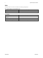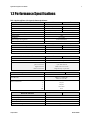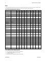
1
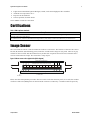
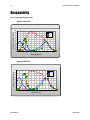
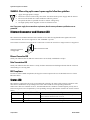
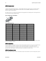
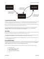
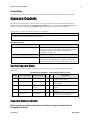
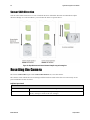
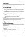
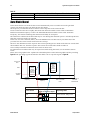
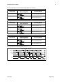
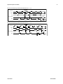
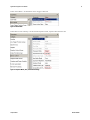
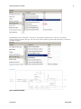
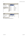
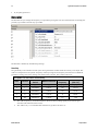
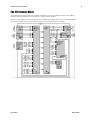
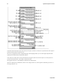
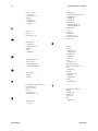
Spyder3 SG-34 GigE Vision Color Manual
57
Appendix B: GPIO Control
The cam era’s General Pu rpose Inpu t / Ou tpu t (GPIO) connector allow s the cam era to receive (and in som e
cases ou tpu t) d irect, real-tim e control signals that are ind epend ent from the Ethernet com m u nications. For
exam ple, the GPIO connector can be u sed to control EXSYN C, PRIN (pixel reset), and d irection signals.
You m ay w ant to u se non -Ethernet control signals becau se Ethernet netw ork protocols introd u ce a sm all bu t
m easu rable and u np red ictable lag that m ay not allow for extrem ely precise and reliable control of cam era
behavior, su ch as line rate, integration tim e, and read ou t d irection.
In general, to configu re the GPIO you need to accom plish three m ain tasks:
1.
Assign a physical cam era pin and signal to a GPIO Inpu t nu m ber.
2.
Map the GPIO Inpu t or Ou tp u t u sing the param eter com m and s located in the Line Trigger Fu nction,
Inpu ts, Ou tpu ts, Direction Control, and Sensor Control grou ps in the GUI. (Please note that this step
has alread y been perform ed for the Beginner level scenarios d escribed below .)
3.
If you w ant to u se ap plications other than those provid ed in the Beginner level exam ples, you can u se
the LUT p rogram m ing langu age to m ap the GPIO Inpu t Configu ration to the GPIO O u tpu t
Configu ration in the Gu ru level.
N ote: the screenshots p resented in this section are from the Cam Expert GUI. If you are u sing a d ifferent GUI
the arrangem ent of the com m and s and param eters m ay be d ifferent.
GPIO Getting Started: Beginner Mode
N OTE: The follow ing instru ctions are based on the d efau lt settings of the cam era. Cam eras are shipped from
the factory in a d efau lt setting. Defau lt settings are restored by load ing the factory d efau lt (see Trigger Settings
(GURU) for d etails).
The GPIO Connector
The GPIO connector is u sed to interface external signals in and ou t of the cam era . The connector contains 15
pins that can configu re 4 inp u ts and 4 ou tpu ts (See Figu re 1 and Table 1). Three of the fou r inpu ts/ ou tpu ts (i.e.
0 to 2) can be configu red as Off, LVDS (Low Voltage Differential Signal), or TTL (Transistor/ Transistor Logic).
The rem aining inpu t and ou tpu t (i.e. 3), can be configu red as either Off or TTL.
Figure 27: GPIO Pinout
Teledyne DALSA
03-032-20124-00