1
PC-AT MultiJimctioll Products
'
ADVANTAGE!N
ASr
IIESEflIIOI INC.
PC-A T Multi/unction
ExpansiuH Board Offering
up 10 3 Mb of I\IJeJ1wr:\, and
PO\\'er/ul I/O Capahililie...
User's Manual Advantage! Memory Expansion and 1/0 Board for the IBM Personal Computer AT
User's Manual
000179-001 C
June, 1985
AST Research, Inc.
Irvine, California
(714) 863-1333
Third Edition (June, 1985)
IBM, PC/AT, and PC-DOS are registered trademarks of International
Business Machines Corporation.
XENIX is a trademark of Microsoft, Inc.
Advantage! and Advantage-Pak are trademarks of AST Research, Inc.
Changes are periodically made to the information contained in this manual;
these changes will be incorporated into new editions.
A Product Comment Form is provided at the back of this publication. If this
form has been removed, please address your comments to: AST Research,
Inc., Attention: Technical Publications, 2121 Alton Ave., Irvine, CA 92714.
AST Research may use or distribute any of the information you supply in any
way it deems appropriate without incurring any obligations whatsover.
Copyright © 1984 AST Research, Inc. All rights are reserved, including those
to reproduce this book or parts thereof in any form without permission in
writing from AST Research, Inc.
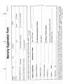
Name
I City
Manufacturer's Name
~_ _ _ _ _ _ _ _ _ _ _ __
---
Version of Network Software Being Used;
See Diskette Label _ _ _ _ _ _ _ _ _ _ _ _ _ _ __
For PCnet or PCnet II Users:
Host System
For Data Communication Products:
Type of PC Used
I Zip Code
No. of PCs at this Address
State
I Phone
000134001 A
Please complete and return this card within (10) days of purchase. AST products are warrantied for one year from date of purchase. If you encounter a problem with an AST product that is under warranty, you should call AST to receive a Return Authorization Number prior to returning the product for service. It is essential that we have your warranty card on file in order for us to provide repair service or replacement at no charge to you. Hard Disk ( _ MB)
Modem ( _ Baud)
Network Card
Data Communication
Graphics (Color? __) _
[ 1 Multifunction/Memory
System Configuration
In order to help us meet your future needs, please fill out the lower portion of this form.
-
Purchased From
Company
Serial No. (See Endflap of Box or Board)
-
First
Purchase Date (mm/dd/yy)
Last
Product Model No. (See Endflap of Box)
Street
MriM.'s "Ms/Mlss Warranty Registration Form
-._ ~- ___-______.-_ 2____-.- _-_______________._.' _____.___ ._ )_________________'_____.__ .__._. _'_.______.-)___._____.__ .
'--
-,._-
!
--'-
---'- -'-'-
~ ~- ~. -'~ ---_._-(
Attn: Product Marketing 2121 Alton Avenue Irvine, California 92714 AST Research, Inc.
POSTAGE WILL BE PAID BY ADDRESSEE
~~L~LNES~.,~:;~LY IV!,~~~
- --.- -.~ (- - - ~-'~ ~-"- ~~--'- --~.- -~--- -'-'- - {--'
NO POSTAGE NECESSARY IF MAILED IN THE UNITED STATES ---.-
)
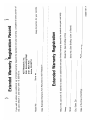
Extended Warranty Registration Record
)
Serial No.
Keep this portion for your records.
Date of Purchase (mm/dd/yy) _ _ _ _ _ _ _ _ _'_ __
Purchased From 040001-001 A
Serial No. (See Endflap of Box or Board) Street
City, State, Zip _ _ __ Model No. (See Endflap of Box) _ _ _ _ _ _ _ _ _ __ Name
Return this card with U.S. $50.00 to obtain an additional one-year limited warranty beyond the standard one-year warranty. Extended Warranty Registration
Date Extended Warranty Form Returned to AST Research _ _ __
Model No. _ __
AST Research, Inc.
Attn: Accounting Dept.
2121 Alton Ave.
Irvine, CA 92714
If you wish to obtain one additional year of limited warranty beyond the standard one-year warranty. complete the lower portion of
this card. detach it, and return with U.S. $50.00 to:
)
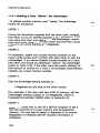
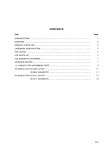
TABLE OF CONTENTS
SECTION 1. INTRODUCING THE ADVANTAGE! ........
1.1 Inventory Checklist . . . . . . . . . . . . . . . . . . . . . . . . .
1.2 Related Reading . . . . . . . . . . . . . . . . . . . . . . . . . . .
1.3 What's In This Manual? .....................
1-1 1-2 1-2 1-3 SECTION 2. OVERViEW ...........................
2.1 Factory Configuration .......................
2.2 Standard Features .........................
2.3 Optional Features ..........................
2.4 AT System Requirements ....................
2-1 2~ 1 2-3 2-3 2-4 SECTION 3. CONFIGURATION AND INSTALLATION ... 3-1 3.1 Before You Begin .......................... 3-2 3.2 Configuring the Advantage! .................. 3-2 STEP 1-Configuring the Memory Size ........ 3-4 STEP 2-Configuring the Memory Starting Address .......................... 3-7 Option #1: Split Memory Addressing in a 256K AT ............ 3-8 Option #2: Split Memory Addressing in a 512K AT ............ 3-9 Option #3: Contiguous Memory Addressing in a 512K or 640K AT ........ 3-11 STEP 3-Selecting Error Checking ........... 3-12 STEP 4-Configuring the Serial Ports ......... 3-14 STEP 5-Configuring the Parallel Port ........ 3-16 STEP 6-Configuring the Game Port ......... 3-17 STEP 7-lnstalling the Advantage! in the AT ... 3-19 STEP 8-Run the AT SETUP and Diagnostic Program ......................... 3-24 SECTION 4. MEMORY CONFIGURATION ............. 4-1 4.1 AT Memory Addressing ..................... 4-1 4.1.1 The 640K Base Area-Split Memory Addressing .......................... 4-3 iii
TABLE OF CONTENTS
(Continued)
4.2 4.3 4.4 4.5 4.1.2 The 15 Megabyte Expansion Memory Area. . . . . . . . . . . . . . . . . . . . . . . . . 4-6 4.1.3 AT System Board Memory Configuration .. 4-6 Setting the Starting Memory Address of the Advantage! . ............................... 4-7 If You Have Other Memory Cards .............. 4-7 4.3.1 Installing a Card "Below" the Advantage! .......................... 4-8 4.3.2 Installing a Card "Above" the Advantage! .......................... 4-9 Installing Additional Memory on the Advantage!. . . . . . . . . . . . . . . . . . . . . . . . . . . . . . . 4-10 4.4.1 Memory Chip Specifications ............ 4-10 4.4.2 Populating the Memory Rows with Memory Chips. . . . . . . . . . . . . . . . . . . . . . . 4-11 4.4.3 Mixing 64K and 256K Memory Chips .... 4-11 Setting the Memory Size of the Advantage! .... 4-13 SECTION 5. SERIAL PORTS . ......................
5.1 Technical Information About AT Serial Ports ....
5.1.1 I/O Address and Interrupt Assignments ...
5.1.2 Serial Port Pinout Specifications .........
5.1.3 Managing the Advantage! Serial Port Inputs ...............................
5.1.4 Configuring External Serial Devices ......
5.1.5 Programming the Serial Ports ...........
5.1.6 The AT Serial Port Controller ............
5.2 Advantage! Serial Port Configuration ...........
5.3 Advantage! Factory Default Serial Port Configurations .............................
5.4 Installing Advantage! Serial Port #2 ...........
5-1 5-1 5-2 5-2 5-4 5-6 5-6 5-7 5-7 5-9 5-9 SECTION 6. PARALLEL PRINTER PORT . ............ 6-1
6.1 Technical Information About AT Parallel Ports ... 6-1 6.1.1 I/O Address and Interrupt Assignments ... 6-2 iv
'-../ TABLE OF CONTENTS
(Continued)
6.1.2 Parallel Port Pinout Specifications ........
6.1.3 Configuring External Parallel Devices .....
6.1.4 Programming the Parallel Ports ..........
6.2 Advantage! Parallel Port Configuration .........
6.3 Advantage! Factory Default Parallel Port Configuration ..............................
6-2 6-2 6-2 6-4 SECTION 7. GAME ADAPTER PORT ................
7.1 Technical Information About the Game Port .....................................
7.1.1 110 Address and Interrupt Assignments ...
7.1.2 Game Adapter Port Pinouts .............
7.2 Advantage! Game Adapter Port Configuration ...
7.3 Software Compatibility ......................
7.4 Game Port Diagnostic Testing ................
7.5 Installing the Game Port Adapter Upgrade Kit ...
7-1 6-6 7-1 7-1 7-1 7-2 7-3 7-4 7-4 APPENDICES
Appendix
Appendix
Appendix
Appendix
A. Recommended Serial Port Wiring .......... A-1 B. General Serial Interface Wiring Information ..
C. Switching Between Parallel Printer Ports ....
D. Advantage! and AT Memory Configuration Information ............................
Appendix E. Configuring the AT System Board Memory ..
B-1 C-1 D-1 E-1 FIGURES
,..-.,
Figure
Figure
Figure
Figure
2-1. Advantage! Board Layout .................
3-1. Setting the Advantage! Memory Size .......
3-2. Memory Size Example #1 ................
3-3. Memory Size Example #2 .............. ,.
2-2 3-5 3-6 3-6 v
TABLE OF CONTENTS
(Continued)
Figure 3-4. Split Memory Addressing in a 256K AT ..... 3-8 Figure 3-5. Split Memory Addressing in a 512K AT .... 3-10 Figure 3-6. Contiguous Memory Addressing in 512K or 640K AT ........................... 3-11 Figure 3-7. Enabling and Disabling Parity ............ 3-13 Figure 3-8. Game Port Enable ..................... 3-17 Figure 3-9. AT System Board Memory Configuration ... 3-20 Figure 3-10. Serial Port #2 and Game Port Connector Locations ............................. 3-22 Figure 4-1. AT System Memory Map .................. 4-2 Figure 4-2. Split Memory Addressing .................. 4-5 Figure 4-3. Advantage! Memory Row Configuration ..... 4-11 Figure 4-4. Switch Block #1 and Memory Rows ........ 4-14 Figure 4-5. Memory Size Example #1 ............... 4-15 Figure 4-6. Memory Size Example #2 ............... 4-16 Figure 5-1. DB9 to DB25 Serial Port Conversion Pinouts . 5-3 Figure 5-2. Serial Port Interface Using DB9-DB25 Adapter Cable ...... . . . . . . . . . . . 5-3 Figure 5-3. Serial Port Input Line Configuration Block .... 5-5 Figure 5-4. Switch Block #2 and IRQ Enable Block Location " . . . . . . . . . . . . . . . . . . . . . . . . 5-7 Figure 5-5. Default Settings with One Serial Port ........ 5-9 Figure 5-6. Default Settings with Two Serial Ports ....... 5-9 Figure 6-1. Switch Block #2 and IRQ Enable Block Location. . . . . . . . . . . . . . . . . . . . . . . . . . . 6-4 Figure 6-2. Default Configuration of Parallel Port ........ 6-6 Figure 7-1. Game Adapter Port EnablelDisable Switch ... 7-3 Figure B-1. Ideal Case: DTE to DCE Interface .......... B-4 Figure B-2. Typical DTE to DTE Interface .............. B-6 Figure B-3. DTE to DTE (NEC 7700 Printer) Interface .... B-7 Figure B-4. Serial Interface Form ..................... B-9 Figure E-1. AT System Board Memory Configuration ..... E-2 vi
TABLE OF CONTENTS
(Continued)
TABLES
Table 3-1. Configuration for Advantage! with One Serial
Port ................................... 3-14 Table 3-2. Configuration for Advantage! with Two Serial Ports .................................. 3-15 Table 3-3. Parallel Port Configuration in AT with Color-Type Display Card .................. 3-16 Table 3-4. Parallel Port Configuration in AT with Monochrome-Type Display Card ............ 3-1,7 Table 5-1. AT Serial Port 1/0 Address & IRQ Assignments 5-2 Table 5-2. DB9 Serial Port Pinouts .................... 5-2 Table 5-3. Configuration for Advantage! with One Serial Port ........................... 5-8 Table 5-4. Configuration for Advantage! with Two Serial Ports. . . . . . . . . . . . . . . . . . . . . . . . . . 5-8 Table 6-1. AT Parallel Port 1/0 & IRQ Assignments (with Monochrome-Type Display Card) ........ 6-2 Table 6-2. AT Parallel Port 1/0 & IRQ Assignments (with Color-Type Display Card) .............. 6-2 Table 6-3. AT Parallel Port Pinouts ................... 6-3 Table 6-4. Parallel Port Configuration in AT with Monochrome-Type Display Card ............. 6-5 Table 6-5. Parallel Port Configuration in AT with Color-Type Display Card ................... 6-5 Table 7-1. Game Adapter Port Pinouts ................ 7-2 Table D-1. Split Memory Addressing Memory Allocation .. D-2 Table D-2. Switch Block #3 Settings (Starting Address) ... D-3 vii
(This page intentionally left blank)
viii
SECTION 1
INTRODUCING THE ADVANTAGE!
The AST Advantager" is a versatile multifunction enhancement
product for the IBM Personal Computer (PC) AT. The
Advantage! includes these features:
• Memory expansion upgradable to 1.5 Megabytes
(MB) on the main board and 3 MB total using the
Advantage-Pak piggyback memory module.
• "Split Memory Addressing" which allows the
Advantage! to round out your AT base memory to
640K while also providing expansion memory at
1 Megabyte and above. This provides the greatest
possible efficiency in AT memory usage.
• Compatibility with both 64K and 256K RAM chips for
maximum flexibility in upgrading Advantage! memory.
Total memory capacity of the Advantage! (with
Advantage-Pak installed) is 768KB using 64K chips,
or 3MB using 256K chips.
• Two RS-232 asynchronous serial communications
ports; one standard and one optional.
• A parallel printer port.
• An optional game adapter port.
1-1
Introducing the Advantage!
1.1 Inventory Checklist
Before you get started, check that your Advantage! package
includes the following:
• Advantage! circuit board.
• Advantage-Pak piggyback circuit board (if applicable to your memory configuration). • Serial port #2 interface ribbon cable and bracket (if the second serial port option is included on your Advantage! board). • Game adapter port ribbon cable and bracket (if the game port option is included on your Advantage! board). NOTE
Be sure to fill out your warranty card (located at the front of this manual) and mail it in. 1.2 Related Reading
This manual assumes some familiarity with the PC-DOS
operating system and the IBM PC-AT hardware. All references
to operating system commands and 1/0 port designations in
this manual assume operation under a single-user, single
tasking version of the PC-DOS operating system.
1-2
r-..
Introducing the Advantage!
You can find additional information in the following manuals
for your IBM PC-AT:
•
Installation and Setup
•
Guide to Operations
•
Technical Reference
•
Disk Operating System
•
BASIC
1.3 What's In This Manual?
Section 2 gives an overview of the Advantage! product,
including a diagram locating all the important
Advantage! features.
Section 3 describes how to configure the Advantage! and
install it in your AT.
Section 4 describes Advantage! memory configuration in
detail.
Section 5 describes the Advantage! serial ports in detail.
Section 6 describes the Advantage! parallel printer port in
detail.
Section 7 describes the Advantage! game adapter port in
detail.
Appendix A describes recommended wiring configurations for
specific serial devices such as printers and
modems.
1-3
Introducing the Advantage!
Appendix B is a "primer" on serial port interfaces.
Appendix C describes a utility program that routes printer
output from one parallel port to another.
Appendix D lists all the possible settings for Advantage!
Switch Block #3 (starting memory address).
Appendix E describes how to properly configure the AT
system board for either 256K or 512K of system
board memory.
1-4
SECTION 2
OVERVIEW
This section describes the standard and optional features of
the Advantage!, as well as AT system requirements for
Advantage! installation.
2.1 Factory Configuration
The Advantage! is shipped from the factory in this
configuration:
• Parallel port configured as LPT1, for use in an AT
with a color-type display card which does not have a
built-in printer adapter port.
• Serial port #1 configured as COM1 using interrupt
line IRQ4 (Standard).
• Serial port #2 configured as COM2 using interrupt
line IRQ3 (Optional-disabled if not installed).
• Game port enabled (Optional-disabled if not
installed).
• Split Memory Addressing enabled (factory setting
may be for either 256K or 512K AT system board
check before installing).
• Memory size switches set as appropriate for the
factory-installed RAM on your Advantage!.
2-1
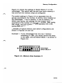
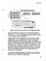
N
I
N
"T1
Row 1
C
o
-
'<
I»
r
a
I»
I II
'o
~ S'
:::.
;;
~
J3-Serlal Port #2 Connector J7-Serial Port #1
RS232C Configuration Block
() C1I
JS
U
'
SW3-Swltch Block #3
(Starting Address)
SW2-Swltch Block #2
(Port Enable)
=
~..,u~.
Ute
(
"C=::J c=J }
CJ2
SW1-Swltch Block #1
(Memory Configuration)
TP'Od ''"'I' [==:J
UII
U
-
"1~c=J
CJ
11crc==::J
use
=
""". useo::::::::=::::J ~ Dll~'Ic=2
~
;;::;
,0
)
= elt
=
I
",II
r - - l " , II c==J'''DI
~~~
.....
(
)
,o0~0~~~~~~~~~~~~~~I~~~~tg~1 Illi Ilf~ "
!'. ~~ ~I @~ ~~ @bJ~ ~- l~:J ~- ~bl @
~
~
I
~
I
@@~.~~ ;~~,~~~ II:
t;J
~
=.~
1
'" ~ 0~"@ ~ 0@~ 0~ ~ ~ 0~ ~ ~ ~I ~ g,~~~
J5-Advantage-Pak
Connector
Q. Row 3 :to
I
N
...
cS' c
iiJ Row 2
J4-Game Port Connector
J8-Serial Port #2
RS232C Configuration Block
I'D
=:
<
ii'
o<
Overview
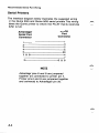
2.2 Standard Features
These are the standard Advantage! features:
• A minimum of 128K bytes of Random Access
Memory (RAM).
• An RS-232C serial port.
• A parallel printer port.
2.3 Optional Features
These options are available for your Advantage!:
• Memory expansion is available in increments of
either 128KB (using 64K RAM chips) or 512KB
(using 256K RAM chips) for up to a total of 1.5MB
on the Advantage! main board.
• The Advantage-Pak piggyback memory module adds
up to 1.5MB to this, making the maximum possible
memory of the Advantage! package 3MB.
• A second serial port (AST Model No. ADV-OOOS) that
can be configured as COM2.
• A game adapter port (AST Model No. ADV-OOOG)
that can be used with one or two IBM-compatible
joysticks or other acceptable cursor control device.
These options may be factory-installed, or you may install
them yourself at a later date. Upgrade kits are available from
your dealer.
2-3
Overview
NOTE
Although the AST Research Advantage!
card is designed for easy user expansion,
the warranty coverage applies only to the
configuration of the board as originally
shipped from the factory. Components
added on at a later date are not warrantied.
2.4 AT System Requirements
The Advantage! board and Advantage-Pak memory module
are designed to be completely compatible with the IBM PC-AT.
There are no special requirements for installing the Advantage!
in the AT except those not~d during the installation instructions.
All references to operating system commands and I/O port
designations in this manual assume operation under a single
user, single-tasking version of the PC-DOS operating system.
2-4
SECTION 3
CONFIGURATION AND INSTALLATION
This section contains instructions for installing your Advantage!
in most AT configurations. There are eight basic steps to
follow when installing the Advantage!:
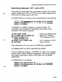
STEP l-Configuring the Memory Size
STEP 2-Configuring the Starting Address
STEP 3-Selecting Error Checking
STEP 4-Configuring the Serial Ports
STEP 5-Configuring the Parallel Port
STEP 6-Configuring the Game Port
STE,P 7-lnstalling the Advantage! in the AT
STEP a-Running the AT's SETUP and Diagnostic Program
If you have more technical questions about a particular
feature that are not addressed here, please refer to one of
the following sections for further information:
Section 4: Memory Configuration
Section 5: Serial Port Configuration
Section 6: Parallel Port Configuration
Section 7: Game Port Configuration
3-1
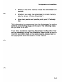
Configuration and Installation
3.1 BEFORE YOU BEGIN •
If your AT is equipped with a 256K system board, or
if you are changing the AT system board memory
configuration at this time, you must configure the
system board according to the instructions contained
in Installation Step 7 (or Appendix E) of this manual.
Failing to do this will cause errors during the AT's
power-on self test.
•
"Base Memory" refers to the AT's 640K standard
memory area, and is directly accessible by PC-DOS.
"Expansion Memory" refers to the AT's 15 Megabyte
extended memory area, and is accessible via VDISK
or other special software.
"Split Memory Addressing" means part of the
Advantage! memory is rounding out the 640K base
area, while the remaining memory provides
expansion memory in the 15 Megabyte area.
"Contiguous Memory Addressing" means that all of
the Advantage! memory is being used as expansion
memory
Refer to Section 4 for further information on these terms.
•
Unless otherwise noted, all references to the
Advantage! include those cards which have the
optional Advantage-Pak piggyback board installed.
3.2 Configuring the Advantage!
To configure the the Advantage!, you need to know these
things:
•
3-2
How much memory is installed on the Advantage!
"........
"-/
Configuration and Installation
• Where in the AT's memory range the Advantage! will
operate
• Whether you want the Advantage! to check memory
data for errors ("Parity Checking")
• How many serial and parallel ports your AT already
has
This information is programmed into the Advantage! by setting
switches and shorting plugs on the card. The following steps
tell you how to do this.
If you have questions regarding Advantage! configuration that
are not answered during the installation steps (such as how to
mix 64K and 256K chips on the same board). please refer to
the appropriate technical section of this manual.
3-3
Configuration and Installation
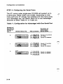
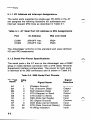
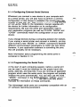
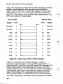
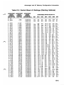
STEP 1-Configuring the Memory Size
Figure 3-1 shows the settings for Switch Block #1 on the
Advantage!. This switch tells the card how much memory it
has and how the memory chips are configured.
The switch settings in Figure 3-1 are separated into six groups
according to the number of memory rows installed on the
Advantage!; 1 row of memory, 2 rows of memory, etc. Within
each group, the settings are then broken down according to
the number of rows populated with 128K (using 18 64K
chips), and those populated with 512K (using 18 256K chips).
Examples of typical memory size switch configurations are
shown in Figures 3-2 and 3-3.
3-4
Configuration and Installation
Advantage!
r----
Row 1
Row 2
Row 3
Advantage-Pak
Row 4
RowS
Row 6
Number of
Rowa Inatalled
on Advantagel Row1 Row2 Row3 Row4 RowS RoWS SW1 SW2 SW3 SW4 SWS
1
128K
512K
OFF OFF OFF OFF ON
OFF OFF ON ON ON
2
2
2
128K 128K
128K 512K
512K 512K
OFF OFF OFF ON OFF
ON OFF OFF OFF OFF
OFF ON OFF OFF OFF
1
3
3
3
3
128K 128K 128K
128K 128K 512K
128K 512K 512K
~12K 512K 512K
4
4
4
4
4
128K
128K
128K
128K
512K
128K
128K
128K
512K
512K
128K
128K
512K
512K
512K
128K
512K
512K
512K
512K
5
5
128K
128K
128K
128K
128K
512K
128K
128K
128K
128K
512K
512K
128K
128K
128K
512K
512K
512K
128K
128K
512K
512K
512K
512K
128K
512K
512K
512K
512K
512K
6
6
6
6
6
6
6
128K
128K
128K
128K
128K
1281<
512K
128K
128K
128K
128K
128K
512K
512K
128K
128K
128K
128K
512K
512K
512K
128K
128K
128K
512K
512K
512K
512K
128K
128K
512K
512K
512K
512K
512K
5
5
5
5
128K
512K
512K
512K
512K
512K
512K
OFF
ON
ON
OFF
OFF
ON
ON
ON
OFF
OFF
OFF
OFF
Obi
OFF
ON
OFF
OFF
ON
OFF
ON
OFF
O,FE
ON
OFF
ON
OFF
OFF
ON
OFF
OFF
Off
OFF
OFF
ON
ON
ON
ON
ON
ON
OFF
ON
ON
ON
ON
OFF
OFF
ON
ON
OFF
OFF
ON
ON
ON
OFF
ON
OFF
OFF
OFF
OFF
ON
ON
ON
ON
ON
OFF
OFF
ON
ON
ON
OFF
ON
ON
ON
ON
ON
OFF
OFF
ON
ON
ON
ON
OFF
ON
ON
ON
ON
OFF
OFF
ON
ON
ON
ON
OFF
ON
OFF
OFF
OFF
OFF
OFF
ON
ON
OFF
OFF
OFF
!!Wi'::'
OFF
ON
OFF
OFF
OFF
Figure 3-1. Setting the Advantage! Memory Size
3-5
Configuration and Installation
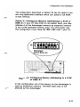
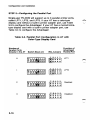
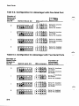
Example 1: If your Advantage! has one row of memory
conSisting of 128K, you would use the first entry
in the table, and set Switch Block #1 as shown in
Advantage!
Switch Block #1
Figure 3-2. Memory Size Example #1
Example 2: If your Advantage! has four rows of memory
(including the Advantage-Pak piggyback board),
and the first row has 128K while rows 2, 3, and 4
have 512K, you would set Switch Block #1 as
shown in Figure 3-3.
Advantage!
Switch Block #1
Figure 3-3. Memory Size Example #2
Set the switches to match the amount of memory on your
Advantage! .
3-6
Configuration and Installation
STEP 2-Configuring the Starting Memory Address
The next thing you need to tell the Advantage! is where its
memory will be located in the AT's memory addressing range.
This is done by configuring the settings of Switch Block #3 on
the Advantage!.
When configuring Switch Block #3, note the following:
• If you are using no other memory cards in your AT,
follow the instructions in this section.
• If you are using the IBM 128K memory card in your
AT, follow the instructions in this section.
• If you are using any other memory cards in your AT
(excluding the IBM 128K card), or if you are using
more than one Advantage!, follow the instructions in
Section 4.3, "If You Have Other Memory Cards".
• If you have 256K on your AT system board, you must
use Option #1 below to configure Switch Block #3.
(You must also configure your AT system board;
instructions for doing so will be given later in Installation
Step 7, as well as in Appendix E of this manual.)
• If you have 512K on your AT system board, you may
use either Option #2 or Option #3 to configure Switch
Block #3.
• Appendix 0 lists all possible starting address switch
settings for the Advantage!.
The starting memory address of the Advantage! should be
selected from one of the following three options, depending
on the configuration of your AT:
• Option #1-Split Memory Addressing in a 256K AT.
This Advantage! configuration is mandatory in all
256K ATs.
3-7
Configuration and Installation
• Option #2-Split Memory Addressing in a 512K AT
• Option #3-Contiguous Memory Addressing in a
512K or 640K AT
If the configuration you want does not fall into one of the
above three categories, please refer to Section 4.
Option #1-Split Memory Addressing in a 256K AT: If your
AT has 256K on its system board, you must enable Split
Memory Addressing on the Advantage! using the switch
settings in Figure 3-4.
Figure 3-4. Split Memory Addressing in a 256K AT
In this configuration, the first 384K of memory on the
Advantage! is dedicated to rounding out the AT's base
memory area to its 640K maximum.
3-8
Configuration and Installation
Please note the following facts regarding Advantage!
installation in a 256K AT:
• If the Advantage! has more than 384K on it, the first
384K is used to round out the AT's base memory to
640K, with the remaining Advantage! memory addressed
as expansion memory.
• If the Advantage! has 384K or less on it, this
memory is added to the AT's 256K system board
memory, for total base memory of 384K, 512K or
640K. There would be no expansion memory in the
15 MB extended memory area.
• If you are installing the Advantage! in a 256K AT, or
if you are changing the AT system board memory
configuration at this time, you must properly configure
your AT system board. Instructions for doing so are
given later in Installation Step 7, as well as in
Appendix E of this manual.
3-9
Configuration and Installation
Option #2-Split Memory Addressing in a 512K AT: If your
AT has 512K on its system board, you may use the first 128K
of memory on the Advantage! to round out the AT's base
memory area to its 640K maximum by setting the Advantage!
switch settings as shown in Figure 3-5.
Figure 3-5. Split Memory Addressing in a 512K AT
In this configuration, the first 128K of memory on the
Advantage! is dedicated to rounding out the AT's base
memory area to its 640K maximum.
• If the Advantage! has exactly 128K on it, this
memory is added to the 512K system board memory,
for total base memory of 640K. There would be no
expansion memory in the 15 MB extended memory area.
• If the Advantage! has more than 128K on it, the first
128K is used to round out net base memory to
640K, with the remaining Advantage! memory
addressed as expansion memory.
3-10
Configuration and Installation
The configuration described in Option #2 may be useful if you
are using application software which can access a full 640K
of base memory.
Option #3-Contiguous Memory Addressing in a 512K or
640K AT: If your AT has 512K on its system board, you may
address all of the Advantage! memory as expansion memory
in the 15 MB extended memory area. You should also use
this configuration if you have the IBM 128K card in your AT.
Figure 3-6. Contiguous Memory Addressing in a 512K
or 640K AT
In this configuration, all of the memory on the Advantage! is
used as expansion memory. The 640K base area is not
affected by the Advantage!.
3-11 Configuration and Installation
STEP 3-Selecting Error Checking
The Advantage! fully supports the AT's memory error checking
feature. This error checking feature is called "Parity Checking".
When parity checking is enabled, if a memory error occurs on
the Advantage!, a parity error will be generated and an error
message will appear on the screen. If an error occurs while
parity checking is disabled, no message would be generated
and you would have no way of knowing there was an error. It
is therefore recommended that you leave this switch on so
that memory errors will not go undetected. The Advantage! is
factory configured with parity enabled.
Disabling parity checking on the Advantage! does not affect
the error-detecting capability of the AT's built-in system board
memory.
Switch Block #1, Position 8, on the Advantage! enables or disables parity checking. Setting this switch ON enables parity
checking, while setting this switch OFF disables parity
checking. 3-12
I"""., ~
Configuration and Installation
Advantagel
Switch Block #1
Figure 3-7. Enabling/Disabling Parity
3-13 Configuration and Installation
STEP 4-Configuring the Serial Ports
The AT running under single-user PC-DOS will support up to
2 serial ports, called COM1 and COM2. Depending on how
many ports your AT already has installed and how many ports
your Advantagel has, set Switch Block #2 on the Advantage!
according to either Table 3-1 or Table 3-2.
Table 3-1. Configuration for Advantagel with One Serial Port
Number of
Serial Ports
Already in
the AT
o
Switch Block #2
IRQ Jumpers
Function of
Advantage!
Serial Ports
Serial #1 functions
as COM1
.
Serial #2 disabled
Serial #1 functions
as COM2
Serial #2 disabled
2
3-14 Serial #1 disabled
Serial #2 disabled
Configuration and Installation
Table 3-2. Configuration for Advantagel with Two Serial Ports
Number of
Serial Ports
Already in
the AT
o
Switch Block #2
IRQ Jumpers
Function of
Advantage!
Serial Ports
Serial #1 functions
as COM 1
Serial #2 functions
as COM2
Serial #1 functions
as COM 2
Serial #2 disabled
2
Serial #1 disabled
Serial #2 disabled
3-15
Configuration and Installation
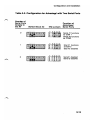
STEP 5-Configuring the Parallel Port Single-user PC-DOS will support up to 3 parallel printer ports, called LPT1, LPT2, and LPT3. If your AT has a color-type
display card without a built-in printer adapter port, use Table 3-3 to configure the Advantage!. If your AT has a monochrome-
type display card with a built-in printer adapter port, use Table 3-4 to configure the Advantage!. r-.. Table 3-3. Parallel Port Configuration in AT with Color-Type Display Card Number of
Parallel Ports
Already in the AT
0
Switch Block #2
IRQ Jumpers
LPT1
rODo8aODD
3-16
r-..
-../
7.5433
rODO~~ODD
Function of
Advantage!
Parallel Port
[:[;1: : : I
LPT2
2
Disabled
3
Disabled
Configuration and Installation
Table 3-4. Parallel Port Con'figuration in AT with Monochrome-Type Display Card Number of
Parallel Ports ,
Already in the AT
(with Monochrome
Card)
Switch Block #2
Function of
Advantage!
IRQ Jumpers Parallel Port
LPT2
2
LPT3
(No Interrupt)
3
Disabled
3-17 Configuration and Installation
STEP 6-Configuring the Game Port
If your Advantage! has the optional game port installed,
enable the port by turning on the appropriate position of
Switch Block #2, as shown in Figure 3-8. If the Advantage!
game port option was factory installed, this switch should
already be on.
Advantagel Switch Block #2
Figure 3-8. Game Port Enable
3-18 Configuration and Installation
STEP 7-Installi ng the Advantagel in the AT
You can install the Advantage! card in expansion slots 2 .
through 6 on the AT system board.
CAUTION
Be sure that the power is off and that the
power cord is removed from the AT before
installing or removing any equipment.
7-A: Remove the AT System Cover
Refer to Section 2 of the IBM AT Installation and Setup manual
if you need instructions on removing the AT system cover.
7-B: Verify AT System Board Configuration
NOTE: If your AT is equipped with a 512K system board, it is
not necessary to perform this step; proceed to Step 7-C.
A jumper on the AT system board (J18) determines the
maximum amount of memory the system board will accept.
With the jumper in the 256K position, the system board will
accept a maximum of 256K; with the jumper in the 512K
position, the system board will accept a maximum of 512K.
This jumper must be in the correct position to ensure reliable
AT operation:
• If you have 256K on your system board and you are
installing a memory board like the Advantage!, the
jumper must be in the 256K position.
• If you have 512K on your system board, the jumper
must be in the 512K position.
The jumper is identified on the system board as "J18" and is
located underneath the disk controller card at the very front of
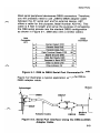
the AT chassis. Figure 3-9 shows the location of this jumper
and its two'configuration positions.
3-19
Configuration and Installation
110
CHANNEL
CONNECTORS
Figure 3-9. AT System Board Memory Configuration
Jumper
3-20
Configuration and Installation
It may be necessary to lift the disk controller card up in order
to gain access to the jumper. To do this, remove the screw
securing the disk controller card bracket to the AT chassis
and carefully lift up the card about 2 inches, being careful not
to put excessive stress on the ribbon cables attached to the
top of the card.
When you have the jumper correctly configured, re-seat the
disk controller card and secure its bracket to the AT chassis
with the screw.
7-C: Install the Advantage! Ribbon Cables
This step is necessary only if your Advantage! has the
optional game port or second serial port installed. If not,
proceed with Step 7-D. Figure 3-10 shows the locations of
these two ports on the Advantage! board.
Locate the ribbon cable(s) for the serial port and/or the game
adapter port. The serial port ribbon cable has a rectangular
10-conductor connector at one end and a male (plug) DB9
connector at the other end. The game adapter port ribbon
cable has a rectangular 16-conductor connector at one end
and a female (socket) DB15 connector at the other end.
Each ribbon cable comes with a bracket. Using the hardware
supplied on the D connectors, mount the D connectors to the
brackets so that when the brackets are installed, the D
connectors will be accessible at the AT's rear panel.
3-21
Configuration and Installation
J3 (Serial Port #2)
J4 (Game Port)
Pin 1
Pin 1
Figure 3-10. Serial Port #2 and Game Port Connector
Locations
Serial Port: Plug the serial adapter cable onto connector J3 on
the Advantage!. Plug the cable onto the board so that Pin 1
on the rectangular connector (indicated by an arrow and the
red or blue stripe on the ribbon cable) aligns with Pin 1 on
the J3 connector, which is silkscreened in white on the circuit
board.
Game Port: Plug the game adapter cable onto connector J4
on the Advantage!. Plug the cable onto the board so that Pin 1
on the rectangular connector (indicated by an arrow and the
red or blue stripe on the ribbon cable) aligns with Pin 1 on
the J4 connector, which is silkscreened in white on the circuit
board.
7-0: Select an Open Expansion Slot
Expansion slot 2, 3, 4, 5, or 6 may be used for the Advantage!
(the slot numbers are visible at the back panel of the AT).
You will need one or two additional slots if you are installing
the optional serial and game port cables in the supplied brackets.
3-22
Configuration and Installation
Locate the metal bracket that covers the cut-out in the back
panel of the AT chassis for the slot that you have selected.
Remove and save the bracket-retaining screw using a small
flathead screwdriver. Remove the bracket. Do the same for
the additional slots used for installing the option port cables if
necessary.
7-E: Install the Advantage! Board
Line up your Advantage! card in the selected slot and position
its front bottom corner in the plastic card guide channel at the
front of the AT chassis. Keeping the top of the Advantage!
card level and any ribbon cables out of the way, lower the
card until its gold edge connectors are aligned with the
system board expansion slot connectors. Using an evenly
distributed pressure, press the Advantage! straight down until
it seats in the expansion slot.
Secure the Advantage! board to the AT chassis using the
bracket retaining screw removed previously.
7-F: Install the Option Cable Brackets
If you are using the supplied brackets to mount your option
port cables, install these brackets into the slot cutouts you
have chosen. Route the cables so they will not be in the way
when you replace the cover.
7-G: Reinstall the AT System Unit Cover
Refer to Section 4 of the IBM AT Installation and Setup
manual for instructions on reinstalling the cover. Use caution
when replacing the cover so that you do not snag any of the
ribbon cables on the Advantage! or any other internal AT
cables.
3-23 Configuration and Insta"ation
STEP 8-Run the AT SETUP and Diagnostic Program
Any time you change the system configuration of your AT by
adding or removing memory or 1/0 ports, you must run the
SETUP program. Instructions for running SETUP are
contained below.
8-A: Diagnostic Program Boot Up
Boot the AT with the IBM "Diagnostics for IBM Personal
Computer AT" diskette. This diskette is found at the back of
the Guide to Operations manual for the AT.
8-B: Run SETUP
Select Option 4, "SETUP." Answer the questions as
appropriate for the new amount of system memory and
expansion memory in your AT.
Some notes about the SETUP program:
• SETUP will ask you a number of questions about
your AT configuration that are unrelated to the
Advantage! installation (for example, it verifies the
type of floppy drive, monitor type, time and date,
etc.). There is no need to change any of these
parameters unless one is in error. SETUP will ask
you to verify correct memory configuration following
these other questions.
• In order to change the amount of expansion
(extended) memory you must first tell SETUP that
you want to change the amount of base memory; re-enter
the correct amount of base memory, then enter the
new amount of expansion memory.
• Appendix D contains two tables which may be
helpful in computing the amount of expansion
memory in your AT in Kilobytes (SETUP wants all
information in Kilobytes):
3-24
Configuration and Installation
Table 0-1 can be used to compute the amount of
base and expansion memory (as well as the net total
memory) in either a 256K or 512K AT, for all possible
Advantage! configurations.
Table 0-2, which gives all the possible switch settings
for Switch Block #3, can also be used to convert
memory size values between Megabytes and Kilobytes.
• When entering the amount of base memory, 256,
384, 512, and 640 are all valid configurations (the
screen display implies that 384K is not permitted).
• When entering the amount of expansion memory,
you can use any 128K value, beginning at zero (0,
128, 256, 384, etc.) up to a maximum of 15360
(15 Megabytes).
• Note once again that if you have 256K on your AT
system board, the Advantage! should be configured
for Split Memory Addressing. Unless you have more
than 256K of base memory (either by filling the system
board with chips or by using Split Memory Addressing
on the Advantage.0, SETUP will not recognize any
expansion memory.
After the system completes the Setup procedure, it will reboot
and reenter the diagnostics.
SOC: Test the New Configuration
Referring to Section 2 of the IBM Guide to Operations manual
for instructions, run the system diagnostics to test your new
configuration.
This completes the installation of the Advantage!.
3-25
(This page intentionally left blank)
3-26 SECTION 4
MEMORY CONFIGURATION
The advanced memory design characteristics of the Advantage!
give it outstanding flexibility. Besides being able to add up to
3 Megabytes to your AT, you can usually install the Advantage!
alongside other AT-compatible memory cards (including other
Advantage! cards) to increase memory capacity beyond 3
Megabytes. The Advantage! also has a unique feature called
Split Memory Addressing. This allows the Advantage! to round
out the AT's base memory to its 640K maximum, while also
giving you additional memory in the AT's 15 Megabyte
expansion memory area.
This section describes the AT's memory addressing capabilities
and how the Advantage! can be utilized to make the most of
these features. Also discussed are how to expand the Advantage!
memory yourself, and how to use the Advantage! along with
other memory cards in your AT.
4.1 AT Memory Addressing
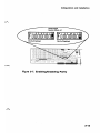
Figure 4-1 illustrates a simplified system memory map for the AT:
4-1
Memory Configuration
------16 Megabytes
15 Megabyte
AT Expansion
Memory Space
384K Reserved Memory
128K Open Memory
640K Base Area
1 Megabyte
PC Address Space
512K System Board
Memory
Figure 4-1. AT System Memory Map
4-2
Memory Configuration
If you are familiar with the standard IBM PC memory map,
you will note that the first Megabyte of the AT is organized
the same as the PC: 640K user memory, followed by 384K
reserved for internal use by the computer. This adds up to 1
Megabyte of memory, the maximum a regular PC can use.
The AT, on the other hand, has the capability of using memory
above the 1 Megabyte limit of the PC, up to a total of 16
Megabytes. This additional 15 Megabyte space in the AT is
called Expansion Memory, while the 640K space is called
Base Memory.
4.1.1 The 640K Base Memory Area-Split Memory
AddreSSing
The AT system board comes populated with either 256K or
512K of memory. In either case, the AT is short of its
maximum 640K base memory. When your AT has 512K, a
separate 128K card can be used to bring the AT's base
memory up to its maximum of 640K. However, this has the
disadvantage of using up an extra slot. Any additional
expansion memory cards would of course require further
slots.
The Advantage!, on the other hand, can be used to round out
the base memory to a full 640K, while also providing
expansion memory. This feature is called Split Memory
AddreSSing.
If your AT has 256K on its system board, you must use the
Split Memory Addressing feature on the Advantage!. In this
case, the Advantage! contributes up to 384K to the 640K
base memory, depending on how much memory is available
on the Advantage!. If you have other than 256K or 512K in
your AT base memory (e.g., 384K). the Advantage!- must be
used as expansion memory only.
4-3
Memory Configuration
If your AT has 512K on its system board, you have two
options for configuring the Advantage!: Split Memory
Addressing allows it to round out the AT's 640K base
memory. Or you can use all the Advantagel memory as
expansion memory. Operating the Advantage! in the Split
mode will cause it to contribute 128K to the AT's 640K base
memory.
For example, if you have a 512K AT and a 1.5 MB Advantage/,
and you want to use Split Memory Addressing to round out
the base memory of the AT to 640K, this would result in 640K
base memory and 1.375 MB (1.5 MB minus 128K) of expansion
memory. This configuration is illustrated in Figure 4-2.
4-4
Memory Configuration
------ 16 Megabytes
15 Megabyte
AT Expansion
Memory Space
1.375 MB
Advantage! Expansion Memory 384K Reserved Memory
128 Advantagel
Split Memory
640K
Base
Area
1 Megabyte
PC Address Space
512K System Board
Memory
Figure 4-2. Split Memory Addressing
4-5 Memory Configuration
Of course, if you already have another 128K memory card,
the Advantage! can still be used; all of its memory will be
located in the AT's 15 MB expansion memory area.
The Split Memory Addressing feature of the Advantage! is
enabled or disabled when you set the card's starting address
with Switch Block #3. This topic is discussed in detail in
Subsection 4.2.
Note that you can use Split Memory Addressing even if you
have insufficient memory on the Advantage! to round out the
AT's base area to a full 640K. In this case, whatever is
available on the Advantage! is added to the existing AT
system board memory, and there will be no expansion
memory on the Advantage!. (Later, as your memory needs
grow, you can add more memory chips to the Advantage! to
both round out the 640K base memory as well as to provide
expansion memory.)
4.1.2 The 15 Megabyte Expansion Memory Area
Beginning at the 1 Megabyte address, there are 15 Megabytes
of expansion memory space in the AT. This space can be
used for RAM disks such as IBM's VDISK.SYS utility, or for
multiuser operating systems such as XENIX. Application software
designed especially for the AT will also be able to utilize this
memory. Figure 4-1 illustrates this 15 Megabyte area.
Memory installed in the 15 Megabyte expansion memory area
must be contiguous, and must start at the 1 Megabyte address
boundary. No gaps are allowed.
4.1.3 AT System Board Memory Configuraton
The AT system board may be configured with either 256K or
512K. A jumper on the system board determines whether the
maximum system board memory is 256K or 512K. Whenever
4-6
Memory Configuration
you add or remove chips on the system board, or when you
install an Advantage! card, you should verify correct
configuration of this jumper. Appendix E contains the
necessary instructions for configuring this jumper.
4.2 Setting the Starting Memory Address of the
Advantage!
The starting memory address of the Advantage! must be set
so that it fits into the AT system memory map without conflicting
with other memory. The Advantage! (along with any other
memory cards) must also fit into the memory map in such a
way that there are no gaps.
Switch Block #3 on the Advantage! is used to set its starting
address. If you are using no other memory cards or if you
have only the IBM 128K card, the instructions in Topic 3.1,
Step 2, will tell you exactly how to set Switch Block #3 on the
Advantage!.
Appendix D illustrates all the possible combinations of
settings for Switch Block #3 on the Advantage!.
4.3 If You Have Other Memory Cards
The Advantage! can usually be installed along with other AT
memory cards, including IBM's, without causing any problems.
However, you must be careful to set the starting addresses
for each card so they do not conflict with each other.
NOTE
If the only other memory card in your AT is
the IBM 128K board, use the recommended
settings in Topic 3.1, Step 2, for Switch
Block #3 on the Advantage!.
4-7
Memory Configuration
4.3.1 Installing a Card "Below" the Advantagel
To address another memory card "below" the Advantage!,
follow this procedure:
STEP 1
Using the instructions supplied with the other card, configure
the other card so its starting address is at 1 Megabyte. If you
are using more than one card below the Advantage!, ensure
that they do not conflict with each other and that they occupy
contiguous memory starting at 1 Megabyte.
STEP 2
If necessary, disable any unused memory sockets on the other cards so they won't conflict with each other or with the Advantage!. If you cannot disable unused sockets on a card, the other card should be addressed "above" the Advantage! (refer to Topic 4.3.2). If the other card has switch settings for
the amount of memory on it, then it will probably automatically disable any unused memory sockets. STEP 3
Set the Advantage! starting address to :
1 Megabyte plus the size of the other card(s)
For example, if the other card has 512K of memory, set the
Advantage! starting address to 1.5 Megabytes, which is
hexadecimal address :180000 (refer to Appendix D).
STEP 4
Install the cards and run the AT's SETUP program to tell it
the new amounts of (1) base memory and (2) expansion
memory. You can use the tables in Appendix D to convert
Megabytes to Kilobytes (SETUP requires information in
Kilobytes).
4-8
r".. Memory Configuration
4.3.2 Installing a Card "Above" the Advantage!
To address another card "above" the Advantage, follow this
procedure:
STEP 1
Set the Advantage! starting address to one of the first three
entries in the tables in Appendix D. Use the first entry if your
AT has 256K on the system board. Use the second entry if
your AT has 512K on the system board and you want to use
Split Memory Addressing. Use the third entry if you do not
want Split Memory Addressing or if you have the IBM 128K
board.
STEP 2
Referring to the instructions supplied with the other card, set
the other card's starting address to:
1 Megabyte plus the amount of expansion memory on the
Advantage!
For example, if the Advantage! has 1.5 Megabytes of
expansion memory on it, you would set the other card's
starting address at 2.5 Megabytes, which is hexadecimal
address :280000.
If you are using Split Memory Addressing on the Advantage!,
remember that the amount of expansion memory is the total
Advantage! memory minus the amount it contributes to the
640K user memory area. Using the above example, a 1.5
Megabyte Advantage! with Split Memory Addressing enabled
in a 512K AT would have 1.375 Megabytes of expansion
memory (1.5 MB minus 128K), so you would set the other
card's starting address at 2.375 Megabytes (1 MB + 1.375 MB),
which is hexadecimal address :260000.
4-9
Memory Configuration
STEP 3
Run the AT's SETUP program and configure it for the new
amounts of (1) base memory and (2) expansion memory. You
can use the tables in Appendix D to convert Megabytes to
Kilobytes (SETUP requires information in Kilobytes).
4.4 Installing Additional Memory on the Advantage!
On the Advantage! and Advantage-Pak, a memory row which
is populated with 18 64K memory chips contains 128K bytes
of memory, while a row populated with 18 256K memory
chips contains 512K bytes of memory:
(18) 64K Chips = 128K Bytes (64K 16-Bit Words)
(18) 256K Chips = 512K Bytes (256K 16-Bit Words)
An Advantage! or Advantage-Pak which is not fully populated
can be upgraded with additional memory simply by plugging
in additional memory chips. You can also upgrade from 64K
chips to 256K chips. AST offers 128K memory upgrade kits
for the Advantage! and Advantage-Pak, consisting of 18 64K
chips; order AST part number MPAD-128. AST also offers
512K memory upgrade kits consisting of 18 256K chips; order
AST part number MPAD-512.
4.4.1 Memory Chip Specifications
If you purchase memory chips from another source, be sure
they meet the following specifications.
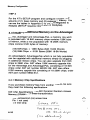
64K Chip Specifications. Use 64K Dynamic Random Access
Memory (DRAM) with these characteristics:
150 nanosecond (ns) access time Pin 1 not used + 5 Volt Only
(; M VI. "'L
f"oR
8 MI-\.~
USE.
4-10
($~e.
p\\5.
{\'I s
,
120 ",S c...\...ifs
O\.J.J.e",J..uV"')
r-..
Memory Configuration
.----~ ~ ~
The
"'------------------
fOIlO~'~ memory chips are compatible.
/
/Micron Technology MT4264-2 or MT4264-15
Hitachi HM4864-2
NEC 04164-15
Motorola MCM6665AP-15 or MCM6665APAL-15
Fujitsu MB8264-15
Texas Instruments TMS4164-15
I
/
f
256K Chip Specifications. Use 256K Dynamic Random Acces Memory (DRAM) with 150 nanosecond (ns) access time. The following manufacturer's 256K (150 ns) memory chips are compatible:
i
,II
AT & T WCM41256FX-15
Fujitsu MB81256-15
Hitachi HM50256P-15
Mitsubishi M5M4256P
Motorola MCM6256L
Texas Instruments TMS4256-15NL
Toshiba TMM41256P-15
\
r",\
\\
6 MV\-z..
V
f\\ s
\
I
ON'-j
(sa..
o-J...J.e"'J.. ... "'"\.
;;
\,
'-,
'~2 Populating the Memory Rows with Memory
IpS
"-...,., Figure
illustrates the arrangement of th chips on the
a el. Row 1
Row 2
Advantage I
Row 3
Figure 4-3. Memory Row Configuration
4-11 Memory Configuration
The Advantage! main board can have up to three rows of
memory on it, numbered 1, 2, and 3. The optional Advantage-Pak
piggyback memory card provides additional rows of memory,
numbered 4, 5, and 6. This provides up to 3 Megabytes in
the space of a single AT expansion slot.
When adding memory to the Advantage! or Advantage-Pak,
please note the following:
• The memory rows on the Advantage! and Advantage-Pak must be populated in sequential order. You cannot have an empty row of sockets in between two populated rows. • Do not install the Advantage-Pak piggyback board unless all three rows on the Advantage! main board are fully populated. • Whenever you add or remove memory on the
Advantage!, be sure you re-adjust Switch Block #1 to
reflect the new memory configuration on the card.
This topic is discussed in Subsection 4.5.
• You must run the AT's SETUP program any time you add or remove memory from the AT. 4.4.3 Mixing 64K and 256K Memory Chips
When mixing 64K and 256K chips on the same board, please
note the following:
• Each row of 18 chips must be populated entirely, using one type of chip. You cannot intermix 64K and 256K chips in the same row. • Once a row of 256K chips is installed, all the following rows must use only 256K chips. For example, if you have 64K chips in Rows 1 and 2, and you install 256K chips in Row 3, then Rows 4 thru 6 (on the Advantage-Pak) must all use 256K chips. 4·12 "........,
'
Memory Configuration
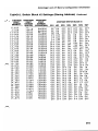
4.5 Setting the Memory Size of the Advantage!
Switch Block #1 on the Advantage! tells the card how much
memory is installed on it. The diagram in Figure 4-4 shows
you the location and settings of Switch Block #1, as well as
the location of the memory rows on the Advantage!.
4-13 Memory Configuration
, - - - - Row 1
Row 2
Row 3
Advantage-Pak
Row 4
RowS
Row 6
Number of
Rows Installed
on Advantage!
Row1 Row2 Row3 Row4 Row5 RowS SW1 SW2 SW3 SW4 SW5
1
1
128K
512K
OFF OFF OFF OFF ON
OFF OFF ON ON ON
2
2
2
128K 128K
128K 512K
512K 512K
OFF OFF OFF ON OFF
ON OFF OFF OFF OFF
OFF ON OFF OFF OFF
3
3
3
3
128K
128K
128K
512K
128K
128K
512K
512K
128K
512K
512K
512K
4
4
4
4
4
128K
128K
128K
128K
512K
128K
128K
128K
512K
512K
128K
128K
512K
512K
512K
128K
512K
512K
512K
512K
5
128K
128K
128K
128K
128K
512K
128K
H28K
128K
128K
512K
512K
128K
128K
128K
512K
512K
512K
128K
128K
512K
512K
512K
512K
128K
512K
512K
512K
512K
512K
128K
128K
128K
128K
128K
128K
512K
128K
128K
128K
128K
128K
512K
512K
128K
128K
128K
128K
512K
512K
512K
128K
128K
128K
512K
512K
512K
512K
128K
128K
512K
512K
512K
512K
512K
5
5
5
5
5
6
6
6
6
6
6
6
128K
512K
512K
512K
512K
512K
512K
OFF
ON
ON
OFF
OFF
OFF
OFF
ON
OFF
ON
OFF
OFF
ON
OFF
OFF
OFF
ON
ON
ON
ON
OFF
ON
ON
ON
OFF
OFF
ON
OFF
OFF
ON
ON
OFF
ON
OFF
OFF
OFF
OFF
ON
ON
ON
OFF
ON
OFF
OFF
OFF
OFF
ON
ON
ON
ON
OFF
OFF
ON
ON
OFF
OFF
ON
ON
ON
OFF
ON
OFF
OFF
OFF
OFF
ON
ON
ON
ON
ON
OFF
OFF
ON
ON
ON
OFF
ON
ON'
ON
ON
ON
OFF
OFF
ON
ON
ON
ON
OFF
ON
ON
ON
ON
OFF
OFF
ON
ON
ON
ON
OFF
ON
OFF
OFF
OFF
OFF
OFF
ON
ON
OFF
OFF
OFF
Figure 4-4. Switch Block #1 and Memory Rows
4-14
Memory Configuration
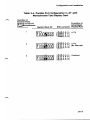
Figure 4-4 shows the settings for Switch Block #1 on the
Advantage!. This switch tells the card how much memory it
has and how the memory chips are configured.
The switch settings in Figure 4-4 are separated into six
groups according to the number of memory rows installed on
the Advantage!; 1 row of memory, 2 rows of memory, etc.
Within each group, the settings are then broken down
according to the number of rows populated with 128K (using
64K chips), and the number of rows populated with 512K
(using 256K chips).
Examples of typical memory size switch configurations are
shown in Figures 4-5 and 4-6.
Example 1: If your Advantage! has one row of memory
consisting of 128K, you would use the first entry
in the table, and set Switch Block #1 as shown in
Figure 4-5.
51
Advantage!
Switch Block #1
Figure 4-5. Memory Size Example #1
4-15 Memory Configuration
Example 2: If your Advantage! has four rows of memory
(including the Advantage-Pak piggyback board),
and the first row has 128K while rows 2, 3, and 4
have 512K, you would set Switch Block #1 as
shown in Figure 4-6.
Advantage!
Switch Block #1
Figure 4-6. Memory Size Example #2
Set the switches to match the amount of memory on your
Advantage!.
4-16 SECTION 5
SERIAL PORTS
The serial ports in the AT provide an asynchronous (async)
serial communications link between the computer and serial
peripheral devices such as modems, serial printers, plotters, a
mouse, or other peripherals which use a serial interface. Data
communication between the computer and the external device
is handled "serially", one bit at a time. There are nine
interface lines available for serial communications between
the computer and the external device: one is used by the
computer to send data, while a second is used by the
computer to receive data. The remaining interface lines may
be used as "handshaking" flags to control the flow of data
back and forth.
An AT running under single-user PC-DOS will support up to
two serial ports. These ports are referred to as COM1 and
COM2 (some IBM manuals also refer to them as Async and
Alternate Async, respectively). COM1 and COM2 are the- only
two serial ports which single-user PC-DOS can access.
The Advantage! can be equipped with either one or two
asynchronous serial communication ports. Serial Port #1 is
standard, and can be configured as either COM1 or COM2.
Serial Port #2 is optional, and can be configured as COM2
only. Either or both ports can be disabled if necessary to
avoid conflicts with other AT serial ports you may already
have. The Advantage! serial ports conform to the RS-232C
communications standard.
5.1 Technical Information About AT Serial Ports
The following technical information applies to the the serial
ports on the Advantage!.
5-1
Serial Ports
5.1.1 1/0 Address and Interrupt Assignments
The serial ports supported by single-user PC-DOS in the AT
are assigned the following hardware 1/0 addresses and
interrupt request (IRQ) lines as described in Table 5-1.
Table 5-1. AT Serial Port 1/0 Address & IRQ Assignments
Port
110 Address
IRQ Line Used
COM1
COM2
3F8-3FF Hex
2F8-2FF Hex
IRQ4 IRQ3 The Advantage! conforms to this standard and uses identical
1/0 and IRQ assignments.
5.1.2 Serial Port Pinout Specifications
~
---./
The serial ports in the AT and on the Advantage! use a DB9P
(plug or male) interface connector with a DTE (Data Terminal
Equipment) interface configuration. The pinout for both ports
is identical at the DB9 connectors and is shown in Table 5-2.
Table 5-2. DB9 Serial Port Pinouts
RS-232C
Name
Cable
Pin #
AA
BA
BB
CA
CB
CC
AB
CF
CD
CE
2
3
4
5
6
7
8
20
22
5-2
1
Signal Name
Signal
Direction
(Chassis Ground)
TxD (Transmit Data)
RxD (Receive Data)
RTS (Request to Send
CTS (Clear to Send)
DSR (Data Set Ready)
SG (Signal Ground)
DCD (Data Carrier Detect)
DTR (Data Terminal Ready)
RI (Ring Indicator)
Common
Output
Input
Output
Input
Input
Common
Input
Output
Input
~
-...../
Serial Ports
Most serial peripheral devices use 0825 connectors. Therefore,
you will probably need to use a OB9-to-OB25 adapter cable
between the AT serial port and the external device. AST
offers a cable for this purpose, Model Number AOV-AC. This
cable is 6 feet in length and serves the purpose of remapping
the OB9 serial pinouts into the standard DB25 configuration
as shown in Figure 5-1. (IBM also offers a similar cable.)
DB9
Connector
DB25
Connector
(AT)
1
2
3
4
5
6
7
8
Carrier Detect DCD
Receive Data RxD
Transmit Data TxD
Data Terminal Ready DTR
Signal Ground GND
Data Set Ready DSR
Reguest to Send RTS
Clear to Send CTS
9
Ring Indicator RI
8
3
2
20
7
6
4
5
22
Figure 5-1. 089 to 0825 Serial Port Conversion Pinouts
Figure 5-2 illustrates a typical application using the DB9-to
OB25 adapter cable.
.
Advantage!
+
Modem
1
r---DB9S
DB9P
r
Adapter Cable
t
Modem
Cable
Figure 5-2. Serial Port Interface Using the 089-to-OB25
Adapter Cable
5-3
Serial Ports
Since most serial devices use the OB25 configuration, the
information in Appendix A and Appendix B is presented in
that format. That is, an assumption is made that you will be
using a OB9-to-OB25 adapter cable between the AT and the
serial device. If this is not the case, substitute the OB9 pin
numbers shown in Figure 5-1 for the OB25 pin numbers used
in Appendix A and Appendix B.
5.1.3 Managing the Advantagel Serial Port Inputs
Because of the way PC-DOS manipulates the serial ports, all
of the input signals on the interface (with the exception of pin
9, Ring Indicator) must be driven by the external device. If
one or more of the inputs is left disconnected or not driven,
PC-DOS may interpret this as meaning that the peripheral
device is not ready and will refuse to communicate with it.
One way to deal with this problem in the AT is to build
special interface cables which shuffle the signals around so
that PC-DOS thinks the external device is ready. Some of the
the. wiring examples used in Appendix A use this technique.
As an alternative, the Advantage! board provides a simple
method for insuring that all the serial port inputs are driven.
Shorting plugs Oumpers) on the Advantage! can be configured
to force one or more of the serial port inputs into a constant
"true" state. This will cause PC-DOS to think that the external
device is ready and allow data transfer to occur. This is done
by configuring shorting plugs on the RS-232C Configuration
Block as shown in Figure 5-3.
5-4
I""""'.
.-/
Serial Ports
/r--r-l-.
rel-.
rel-.--i'
J7
~ .~. ~.
J8
r-l • rel •
654321
Normal (Default): All Inputs
Driven By Connected Device
2-CTS Normal
4-DSR Normal
6-DCD Normal
1-CTS Forced True
3-DSR Forced True
5-DCD Forced True
Ie] •
~.~.~.
Figure 5-3_ Serial Port Input Line Configuration Block
As you can see from Figure 5-3, J7 controls the inputs to
Serial Port #1, while J8 controls the inputs to Serial Port #2.
For each port, you can manipulate (force true) the CTS, DSR,
or DCD inputs, in any combination.
Figure 5-3 shows the shorting plugs in their factory default
configuration; in this configuration, the input lines are left
undisturbed as they enter the card. That is, the external
device is expected to drive all these inputs. To force an input
line true, move the appropriate shorting plug from the "Normal"
position to the "Forced True" position. For example, to force
the DSR input on Serial Port #2 into a constant "true" state,
you would move the shorting plug from J8 pin 4 to J8 pin 3.
Whenever a signal is forced true in this manner, the actual
state of its corresponding input on the DB9 serial port
connector will be ignored.
If you use the wiring diagrams in Appendix A to interface a
serial printer, the shorting plugs shown in Figure 5-3 should
all be left in the "Normal" configuration.
5-5
Serial Ports
5.1.4 Configuring External Serial Devices
Whenever you connect a new device to your computer such
as a serial printer, you will also have to perform a one-time
configuration of that device to establish the correct baud rate,
number of data bits, etc. This usually involves setting switches
on the device. Refer to the installation manual supplied with
the device for further information on its configuration
requirements. Be sure the serial port parameters used by
your application programs (as well as PC-DOS "MODE" and
"OPEN" commands) match the configuration of your serial
device.
1""""'\
'-'"
If you change devices during a computing session (for example,
if you unplug a serial printer and connect a modem), you may
have to enter a new "MODE" or "OPEN" command to establish
different communication parameters to match the new device.
However, if your application software is controlling the ports,
this will probably not be necessary.
More information about programming the serial ports is
contained in Section 5.1.5.
5.1.5 Programming the Serial· Ports
At the start of each computing session, before a serial port can be used it must be initialized for the proper baud rate, parity, data bits, and stop bits. If you are running an application program which uses the serial ports, the program will probably initialize the ports automatically. You can also use the DOS "MODE" command or the BASIC/BASICA "OPEN" command to initialize a serial port. Consult the IBM DOS and BASIC manuals for information on these commands. The Advantage! serial ports are completely compatible with all AT software operating parameters.
5-6
1""""'\ Serial Ports
5.1.6 The AT Serial Port Controller
The serial controller chip used by the AT (and the Advantage.~
is not 100% compatible with the controller used in the PCIXT
line of computers. Therefore, software written for the PC which
uses the serial ports may not function properly in the AT.
5.2 Advantage! Serial Port Configuration
Positions 1, 2, and 3 of Switch Block #2 on the Advantage!
card control the configuration of the Advantage! serial ports.
Shorting plugs on the IRQ Enable Block are used to select
the appropriate interrupt (IRQ) line for each port. The location
of Switch Block #2 and the IRQ Enable Block are shown in
Figure 5-4.
S2-Switch Block #2
IRQ Enable Block
Figure 5-4. Switch Block #2 and IRQ Enable Block
Location
All the possible Advantage! serial port configurations are
shown in Tables 5-3 and 5-4 below. Use Table 5-3 for an
Advantage! with one serial port, or use Table 5-4 for an
Advantage! with two serial ports.
5-7
Serial Ports
Table 5-3. Configuration for Advantage! with One Serial Port
Number of
Serial Ports
Already in
·the AT
Switch Block #2
IRQ Jumpers
o
Function of
Advantage!
Serial Ports
Serial #1 functions
as COM1
Serial #2 disabled
Serial #1 functions
as COM2
Serial #2 disabled
.. ..
••
7
1
;.:!.•. f~.•.:l
3
,
Serial #1 disabled
1 Serial #2 functions
as COM2
Serial #1 disabled
Serial #2 disabled
2
Table 5-4. Configuration for Advantage! with Two Serial Ports
Number of
Serial Ports
Already In
the AT
Switch Block #2
IRQ Jumpers
o
Function of
Advantage!
Serial Ports
Serial #1 functions
as COM 1
Serial #2 functions
as COM2
Serial #1 functions
as COM 2
Serial #2 disabled
Serial #1 disabled
Serial #2 functions
as COM2
2
5-8
r-'-~-'-";;:;"";;"" .
Serial #1 disabled
Serial #2 disabled
Serial Ports
5.3 Advantage! Factory Default Serial Port
Configurations
The factory-set default configuration of the Advantage! serial
ports is shown in Figures 5-5 and 5-6 below. Figure 5-5 is for
an Advantage! with one serial port, while Figure 5-6 is for an
Advantage! with two serial ports.
7 5
••
••
Switch
Block #2
IRQ Enable
Block
Figure 5-5_ Default Settings with One Serial Port
DODD
Advantage!
Switch Block #2
J6
IRQ Enable Block Figure 5-6. Default Settings with Two Serial Ports
5.4 Installing Advantage! Serial Port #2
An upgrade kit is offered by AST for field installation of the
second Advantage! serial port. This upgrade kit, AST Model
Number ADV-OOOS, contains the special components
necessary for proper function of the serial port in an AT. It is
available through your AST Dealer. Instructions for installing
the optional Serial Port #2 are supplied with the upgrade kit.
5-9
(This page intentionally left blank)
5-10 SECTION 6
PARALLEL PRINTER PORT
The parallel ports in the AT provide one-way communication
(output only) between the AT and parallel peripheral devices
such as printers, plotters, or a mouse. Data is sent from the
AT to the external device eight bits (one byte) at a time. The
flow of data is controlled by several "handshaking" lines on
the interface.
An AT running under single-user PC-DOS will support up to
three parallel ports. These ports are referred to as LPT1,
LPT2, and LPT3 (some IBM manuals also refer to the default
port as PRN). These are the only parallel ports single-user
PC-DOS can access.
The Advantage! is equipped with one parallel port as a
standard feature. When the AT is equipped with a monochrome
type display card with built-in printer adapter, the Advantage!
parallel port can be configured as LPT2 or LPT3. When the
AT is equipped with a color-type display card without a built-in
printer adapter, the Advantage! parallel port can be configured
as LPT1 or LPT2.
6.1 Technical Information About AT Parallel Ports
The following technical information applies to the parallel
ports in the AT, including the Advantage!.
6-1
Parallel Printer Port
6.1.1 1/0 Address and Interrupt Assignments
The parallel ports supported by single-user PC-DOS in the AT
are assigned the hardware 110 address and interrupt request
(IRQ) lines as described below. Table 6-1 is for an AT which
is using a monochrome-type display card with a built-in printer
adapter port. Table 6-2 is for an AT using a color-type display
card without a built-in printer adapter port.
Table 6-1. AT Parallel Port 1/0 & IRQ Assignments (with Monochrome-Type Display Card) Port
1/0 Address
IRQ Line Used
Port Location
LPT1
LPT2
LPT3
3BC-3BE Hex
378-37A Hex
278-27A Hex
IRQ7
IRQ5
Not Supported*
Monochrome Card
Add-on Card
Add-on Card
*Interrupt-driven 110 for LPT3 is not supported in the AT.
Table 6-2. AT Parallel Port 1/0 & IRQ Assignments
(with Color-Type Display Card)
Port
LPT1
LPT2
LPT3
1/0 Address
IRQ Line Used
Port Location
378-37A Hex
IRQ7
Add-on Card
278-27A Hex
IRQ5
Add-on Card
- LPT3 Not Supported When Using Color Card
The Advantagel conforms to these standards and uses
identical 1/0 and IRQ assignments.
6.1.2 Parallel Port Pinout Specifications
The parallel ports in the AT and on the Advantagel use a
DB25S (socket or female) interface connector. The pinout for
all the parallel ports is identical and is shown in Table 6-3.
6-2
r-..
Parallel Printer Port
Table 6-3. DB25 Parallel Port Pinouts
LINE
NAME
-STROBE
DO
01
02
03
04
05
06
07
-ACK
BUSY
PE
SLCT
-AUTOFD
-ERROR
-INIT
-SLCT IN
GROUND
AST ADAPTER CABLE
OUTPUT
IBM MATRIX PRINTER
DB25S
CENTRONICS INTERFACE
1
2
3
4
5
6
7
8
9
10
11
12
13
14
32
31
1
2
3
4
5
6
7
8
9
10
11
12
13
14
15
16
17
(18-25)
36
(16,19-30,33)
6.1.3 Configuring External Parallel Devices
Whenever you connect a new device to your computer such
as a parallel printer, you may also have to perform a one-time
configuration of that device to establish desired operating
parameters. This is usually done by setting switches in the
device. Refer to the installation manual supplied with the
device for further information on its configuration
requirements.
6.1.4 Programming the Parallel Ports
Normally no special action is necessary to prepare the parallel
ports for use. However, you can use the PC-DOS "MODE"
command to establish certain parameters such as line width.
Consult the IBM DOS manual for information on this
command.
6-3
Parallel Printer Port
The Advantage! parallel port is completely compatible with all
AT software operating parameters.
6.2 Advantage! Parallel Port Configuration
Positions 4 and 5 of Switch Block #2 on the Advantage! card
control the configuration of the Advantage! parallel port.
Shorting plugs on the IRQ Enable Block are used to select
the appropriate interrupt (IRQ) line for the port. The location
of Switch Block #2 and the IRQ Enable Block are shown in
Figure 6-1.
S2-Switch Block #2
IRQ Enable Block
Figure 6-1. Location of Switch Block #2 and IRQ Enable
Block
All the possible Advantage! parallel port configurations are shown
in Tables 6-4 and 6-5 below. Use Table 6-4 for an AT with a
monochrome-type display card with a built-in printer adapter port,
or use Table 6-5 for an AT with a color-type display card without
a built-in printer adapter port.
6-4
Parallel Printer Port
Table 6-4. Parallel Port Configuration with Monochrome-Type
Display Card Installed
Number of
Parallel Ports
Already in the AT
(with Monochrome
Switch Block #2
Card)
Function of
Advantage!
IRQ Jumpers Parallel Port
LPT2
LPT3
2
(No Interrupt)
Disabled
3
Table 6-5. Parallel Port Configuration with Color-Type Display Card Installed Number of
Parallel Ports
Already in the AT
o
Switch Block #2
IRQ Jumpers
Function of
Advantage!
Parallel Port
LPT1
LPT2
2
Disabled
3
Disabled
6-5
Parallel Printer Port
6.3 Advantage! Factory Default Parallel Port
Configuration
The factory-set default configuration of the Advantage! parallel
port is for an AT with a color-type display card (no other
parallel port installed). This configuration is shown in Figure 6-2
below.
433
J6
Switch Block #2 •••
•••
IRQ Enable
Block
Figure 6-2. Default Configuration of Parallel Port
6-6
SECTION 7
GAME ADAPTER PORT
The game adapter port provides an interface for connecting
one or two joysticks to the AT. With appropriate software, this
device can be used for cursor control, as well as graphics
development and interactive games.
7.1 Technical Information About the Game Port
The following technical information applies to the game
adapter port on the Advantage!.
7.1.1 110 Address and Interrupt Assignments
The game adapter port is assigned I/O addresses 200-207
hex. No hardware interrupt line is used by the game port.
7.1.2 Game Adapter Port Pinouts
The game adapter port uses a DB15S (socket or female)
interface connector. The pinout for this port is shown in Table 7-1.
7-1
Game Adapter Port
Table 7-1. Game Adapter Port Pinouts
(Joystick A)
(Joystick B)
Advantage!
J4 Pin No.
0815 Pin
Number
1
3
5
7
9
11
13
15
1
2
3
4
5
6
7
8
+5VDC
Button 1
X Axis
Ground
Ground
Y Axis
Button 2
+5VDC
2
4
6
8
10
12
14
9
10
11
12
13
14
15
+5VDC
Button 3
X Axis
Ground
Y Axis
Button 4
+5VDC
Signal
Name
A single joystick may be connected directly to the DB15
connector. To connect two joysticks, you will need a special
"Y" connector adapter cable. Consult your dealer for further
information.
7.2 Advantage! Game Adapter Port Configuration
Position 6 of Switch Block #2 on the Advantage! card controls
the configuration of the game port. The location and function
of Switch Block #2 is shown in Figure 7-1.
7-2
Game Adapter Port
Advantagel Switch Block #2
Figure 7-1. Game Adapter Port Enable/Disable Switch
NOTE
The switch should be "OFF" (disabled) unless
your Advantage! has the optional game port
installed.
7.3 Software Compatibility
The game port is totally software-compatible with the IBM
game adapter. However, because a joystick is an analog
device, there may be variations among different joysticks, and
some software may not function as expected even though the
game port is functioning properly. It is therefore recommended
that you make sure that your software includes a joystick
centering function to compensate for differences between
joysticks.
7-3
Game Adapter Port
The program listing in Section 7.4 can be used to test for
proper operation of the game port on the Advantage!.
7.4 Game Port Diagnostic Testing
The Advantage! game port can be tested using the IBM
diagnostics. However, because of a problem in the diagnostic
program, the port may not always show up on the listing of
installed devices. If this is the case, you can use the program
below to test the port. This program requires the use of BASICA
(not BASIC).
10
20
30
40
50
60
DEFINT A-Z:KEY OFF:CLS:STRIG ON:SCREEN 2 PRINT "X1","Y1","S1";"S3" X1 =STICK(0):Y1 =STICK(1) A = STRIG(1 ):C = STRIG(5) LOCATE 3:PRINT X1,Y1,A;C GOTO 30 When you run the above program, moving the joystick in the
X-plane (left-right) causes a change in the "X1" readout, while moving the joystick in the Y-plane (up-down) causes a change in the "Y1" readout. Pressing the switch (either one or two, depending on your joystick) causes the "S1" or "S3" readouts to switch between 0 and -1. Depending on the quality of your joystick, you may not be able to get a zero reading in the X and Y planes when running the program. This is normal and no cause for alarm. 7.5 Installing the Game Port Adapter Upgrade Kit.
An upgrade kit is offered by AST for field installation of the
Advantage! game adapter port. This upgrade kit, AST Model
Number ADV-OOOG, contains the special components necessary
for proper function of the game port in an AT. It is available
through your AST dealer. Instructions for installing the
optional game port are supplied with the upgrade kit.
7-4
'--' APPENDIX A
RECOMMENDED SERIAL PORT WIRING
Appendix A gives the wiring configurations you need to
interface your Advantage! serial port to these serial devices:
1. Modems (such as the Hayes Stack Smart modem,
Novation Cat, and UDS).
2. These serial printers: NEC 7700 series, TI 810
series, Epson MX-100-3, Brother HR-1, OKIDATA
Microline 83A, OKIDATA Microline 84, and the
Anadex 9501.
3. The Qume Sprint 9/45 and 9/55 serial printers.
4. CRTs and printers that run at low baud rates
(110-300 baud).
5. The Diablo 620 printer.
6. The Diablo 630 printer.
7. These serial printers: Smith-Corona TP-1, Epson
MX-80, and IDS Prism.
8.
The Hewlett-Packard H-P 7470A plotter.
For all of these devices:
1. The interface diagrams in this appendix refer to DTE
interfaces (such as the Advantage! serial port) only.
2. A DB25S (female/socket) connector is used for the
Advantage! side and a DB25P (male/plug) connector
for the serial device side. If you use a device that
requires a DB25S (for example, the NEC 7720), you
must use an adapter to connect to the port.
A-1
Recommended Serial Port Wiring
To interface other products to your Advantage! serial port, see
Appendix B (for general information) and your serial device
manual. You can also contact the serial device manufacturer
for advice on connecting the device to an IBM PC-AT
asynchronous serial port.
NOTE
The pin assignments listed in this appendix
are for DB25 connectors; they assume that
you are using an adapter cable to interface
the Advantagel serial port DB9P connector
to a serial device cable DB25S connector. If
you are not using an adapter cable (are
going directly from the DB9 to another DB9
on a serial device cable), then reference
Table 5-1 for DB9 pin assignments, and
substitute the numbers listed there for the
numbers given in this appendix.
Modems
The interface diagram below illustrates the interface between
the Advantage! serial port and modem devices such as the
Hayes Stack Smart modem, Novation Cat, and UDS.
Advantage!
Serial Port
Connector
Modem
Port
Connector
1--------------------------------1
2----------------------------2
3------------------------------3
4----------------------------4
5----------------------------5
6----------------------------6
7------------------------------7
8--------------------------8
20--------------------------20
22----------------------------22
A-2
Recommended Serial Port Wiring
Serial Printers
The interface diagram below illustrates the suggested wiring
for the NEC 7700 series, TI 810 series, Epson MX-100-3,
Brother HR-1, OKIDATA Microline 83A, OKIDATA Microline
84, and Anadex 9501 serial printers. This wiring allows the
printer to inform the PC-AT that its receiving buffer is full.
Printer Port Connector Advantage!
Serial Port
Connector
1----------------------------1
2----------------------------3
3----------------------------2
4----------------------------5
5---------------------.,.----11
5-------------------------19
6 & 8-----------------------20
(TI, Brother, Epson
OKIDATA only
(NEC, Adadex only
7----------------------------7
20----------------------...,.6
&8
NOTE
Advantage! pins 6 and 8 are jumpered
together and connected to printer pin 20.
Printer pins 6 and 8 are jumpered together
and connected to Advantage! pin 20.
A-3 Recommended Serial Port Wiring
Serial Printers
The interface diagram below illustrates the suggested wiring
for the Qume 9/45 and Qume 9/55 serial printers. This wiring
allows the Qume printer to inform the PC-AT that its receiving
buffer is full.
Printer
Port
Connector
Advantage!
Serial Port
Connector
1----------------------------1
2----------------------------3
3----------------------------2
4----------------------------5 5---------------------------20
6 & 8------------------------4
7----------------------------7
20-----------------------6 & 8
NOTE
Advantage! pins 6 and 8 are jumpered
together and connected to printer pin 4.
Printer pins 6 and 8 are jumpered together
and connected to Advantage! pin 20.
A-4
Recommended Serial Port Wiring
Slow CRTs and Printers
The following interface diagram illustrates the suggested
wiring for CRTs and printers that running at low baud rates
(110-300 baud). This wiring does not use standard EIA
RS-232C handshaking, but it should work with most CRTs
and some printers.
Advantage!
Serial Port
Connector
CRT/Printer
Port
Connector
1----------------------------1
2----------------------------3
3----------------------------2
7----------------------------7
4&5
6 & 8-----------------------20
5 & 20
(or 4 & 5 if needed)
NOTE
Advantage! pins 4 and 5 are jumpered
together, and Advantage! pins 6 and 8 are
jumpered together. You can jumper together
CRT/printer pins 5 and 20 or 4 and 5.
Consult the user's manual for your CRT or
printer for your specific configuration.
A-5
Recommended Serial Port Wiring
The Diablo 620 Printer
The interface diagram below illustrates the suggested wiring
for the Diablo 620 serial printer. This arrangement allows the
Diablo to inform the PC-AT side of the interface that its
receive buffer is full.
Advantage!
Diablo 620
Serial Port
Connector
Serial Port
Connector
1----------------------------1
2----------------------------3
3----------------------------2
5----------------------------4
7----------------------------7
6 & 8-----------------------20
20---------------------------6
NOTE
Advantage! pins 6 and 8 are jumpered
together and connected to Diablo 620 pin
A-6
20.
Recommended Serial Port Wiring
Diablo 630 Printers
There are several different versions of the Diablo 630 printer.
AST Research has had the best success with the following
serial interface wiring:
Advantage/
Diablo 630
Serial Port
Connector
Serial Port
Connector
1----------------------------1
2----------------------------3
3----------------------------2
5---------------------------11
7----------------------------7
6 & 8 & 20--------------------6 (or 6 & 4)
NOTE
If this wiring does not work for your 630
Diablo printer, contact Diablo or your printer
dealer.
A-7
Recommended Serial Port Wiring
Serial Printers
The interface diagram below illustrates the suggested wiring
for these serial printers: Smith-Corona TP-1, Epson MX-80,
and IDS Prism. This arrangement gives these printers
sufficient control over output from the PC-AT side of the
interface to allow both devices to remain in a ready state,
while pins 4 and 5 actually control the flow of data from one
side to the other.
Printer
Port
Connector
Advantage!
Serial Port
Connector
1----------------------------1
2----------------------------3
3----------------------------2
4----------------------------5
5----------------------------4
5---------------------------20
6 & 8 & 20
7----------------------------7
6 & 8 & 20
(TP-1 only)
(MX-80, IDS only)
(TP-1 only)
NOTE
Advantage! pins 6, 8, and 20 are jumpered
together and TP-1 printer pins 6, 8, and 20
are jumpered together.
A-8
Recommended Serial Port Wiring
Hewlett-Packard H-P 7470A Plotter
The interface diagram below illustrates the suggested wiring
for the Hewlett-Packard H-P 7470A plotter.
H-P 7470A
Serial Port
Connector
Advantage!
Serial Port
Connector
1----------------------------1
3----------------------------2
2----------------------------3
7----------------------------7
5---------------------------20
6&8&20
NOTE
Advantage! pins 6, 8, and 20 are jumpered
together.
A-9
(This page intentionally left blank)
A-10 APPENDIX B
GENERAL SERIAL INTERFACE
WIRING INFORMATION
This appendix provides general information for wiring your
AST Research Advantage! serial communications ports to
remote devices using the Electronic Industry Association (EIA)
RS-232C standard interface.
NOTE
The Advantage! does not support the
current-loop teletype interface.
The EIA RS-232C standard describes the arrangement of
control and data signals on both sides of a serial communications
interface. Control signals are used to control the flow of data,
and data signals contain the information to be transmitted.
The RS-232C standard describes an ideal case of a data
terminal connected to a modem. A modem (MOdulatorl
DEModulator) is a communications device. The communications
device interfaces to a transmission medium (for example,
phone lines) that carries the signal to a remote, such as a
modem connected to a port on another DTE port or the
communications element of a mainframe computer system.
The RS-232C standard describes the signals that travel
between Data Terminal Equipment (DTE) and Data
Communications Equipment (DCE). The signals control the
exchange of data to and from the local modem and local
terminal. These signals travel on separate wires from pins on
the DTE side (terminal) to pins on the DCE side (modem).
B-1
General Serial Interface Wiring Information
NOTE
The pin assignments listed in this appendix
are for DB25 connectors; they assume that
you are using an adapter cable to interface
the Advantage! serial port DB9P connector
to a serial device cable DB25S connector. If
you are not using an adapter cable (are
going directly from the DB9 to another DB9
on a serial device cable), then reference
Table 5-1 for DB9 pin assignments, and
substitu~e the numbers listed there for the
numbers given in this appendix.
For asynchronous applications (such as the Advantage! serial
communications port) you use only eight or nine signals
between the DTE (your serial port) and the DCE (a modem or
serial device DCE port).
Interfacing DTE to DeE
To familiarize yourself with the signal and sequence requirements
of the RS-232C standard, imagine that you want to connect
the serial port on your AST Research board (DTE) to a telephone
modem (DC E). A correctly configured DCE/DTE interface is
wired straight across: DTE pin 20 wired to DCE pin 20, pin 2
to pin 2, and so forth. The two devices can then interact to
function properly (this interaction is called "handshaking").
When the PC-AT serial port (DTE) wants to transmit data it
raises the voltage on pin 20; pin 20 carries the DTR (Data
Terminal Ready) signal. This voltage travels to DCE pin 20
where the modem (DCE) interprets it to mean that a
communications link is being requested by the terminal
device.
If an open phone line exists, the DCE brings up two lines on
its side of the interface: DSR (Data Set Ready, pin 6) and
DCD (Data Carrier Detect, pin 8). When the DTE (your PC-AT
port) sees high voltage at its pins 6 and 8, it can then bring
B-2
General Serial Interface Wiring Information
If an open phone line exists, the DCE brings up two lines on
its side of the interface; DSR (Data Set Ready, pin 6) and
DCD (Data Carrier Detect, pin 8). When the DTE (your PC-AT
port) sees high voltage at its pins 6 and 8, it can then bring
up pin 4, RTS (Request To Send). RTS tells the DCE that the
DTE has data to transmit to it. The DCE checks that it is
ready to receive data; if so, it brings up pin 5, CTS (Clear To
Send).
Once the DTE sees voltage on its pin 5, it starts transmitting
on the wire connected to pin 2, TxD (Transmit Data). DTE Pin
3, RxD (Receive Data) receives any incoming signals.
Some modems have an automatic answer mode that uses the
signal RI (Ring Indicator, pin 22) to alert the terminal that
incoming data is due. The terminal uses DTR to respond to Rio
CAUTION
To help protect your equipment from
damage, be sure to connect the ground
wires (pins 1 and 7).
B-3
General Serial Interface Wiring Information
Figure 8-1 illustrates an ideal DTE to DCE interface, including signals, signal directions, and sequence (top to bottom). Notice that the DTE (PC-AT side) input signals include DCD, DSR, CTS, and RxD. The DTE output signals include DTR and RTS. The interface must handle these signals before the
DTE can transmit or receive data.
PC-AT Side
Signal
-...../ Modem Side
Pin#
Pin#
DTE
Signal DCE Ground Ground
Ground
7
7
Ground
(RI)
22
22
(RI)
DTR
20
20
DTR
DCD
8
8
DCD
DSR
6
6
DSR
RTS
4
4
RTS
CTS
5
5
CTS
TxD
2
2'
TxD
RxD
3
3
Rxd
...
Figure 8-1. Ideal Case: DTE to DCE Interface
Figure 8-1 illustrates the interface signals in order of
occurrence (top to bottom). From the DTE's standpoint, it
must send DTR, see DeD, see DSR, send RTS, and see CTS
before transmitting or receiving data: the inputs must have
voltage applied to them for the interface to become operational.
(The outputs matter only in that they are inputs to the DCE
side of the interface.) The hardware that controls the DTE
serial interface does not release data to the communications
link until it has received the proper set and sequence of signals.
8-4
~
~
'--"
General Serial Interface Wiring Information
You can think of certain pins on one side of the interface as
"functional pairs"; for example, when the AST serial port
sends DTR, it expects to see DSR (and DCD) raised in
response. DTR and DSR are signal and response to one
another: they act as a pair. The same is true of RTS and
CTS, and of TxD and RxD.
Interfacing OTE to OTE
Many devices, such as serial printers, are set up as DTE. To
output data from your PC-AT serial port (also DTE) to a serial
printer or other DTE device, you must wire a DTE to DTE
interface. A DTE to DTE interface must fool each side of the
link into thinking that it is receiving "response" inputs from a
DCE. The input voltages must be present, and they must
occur in the correct sequence (the correct sequence varies
from device to device).
Each side of a DTE to DTE interface acts like the DTE side of
a DTE to DCE interface. Both sides of the DTE to DTE interface
must send and receive these signals in this sequence before
sending or receiving data:
Send DTR
Receive DCP and DSR
Send RTS
Receive CTS
8-5
General Serial Interface Wiring Information
Figure 8-2 illustrates a DTE to DTE interface, including
signals, signal directions, and sequence.
PC-AT Serial
Port Side
Signal
Qume Sprint 9/45 Serial Printer Pin#
Pin#
DTE
Signal
DTE
Ground
1
Ground
7
7
Ground
DTR
20
20
DTR
DCD
8
8
DCD
DSR
6
6
DSR
RTS
4
4
RTS
CTS
5
5
CTS
TxD
2
2
TxD
RxD
3
3
RxD
Ground
Figure 8-2. Typical OTE to OTE Interface
Notice that the necessary input signals are supplied to both
sides. DCD, DSR, and CTS have voltage applied to them on
either side.
This example does change the ideal sequence by having the
printer OTR signal drive PC-AT signal CTS; however, the
integrated circuit that controls the PC side (INS 8250) is fairly
flexible in reading the sequence of inputs. The reason for the
sequence change is that when the Qume printer receive buffer
is about to fill up it drops its OTR signal. To avoid losing data
by overflowing the printer's receive buffer, we halt PC data
output immediately by dropping the CTS input to the PC side
immediately. The remainder of the interface then "idles" until
the printer raises OTR again. Remember that this is a specific
case for Qume serial printers.
8-6
~
General Serial Interface Wiring Information
Figure 8-3 illustrates another example of interfacing a serial
DTE printer to the PC's Advantage! serial port.
AST Serial Port DTE to NEC 7700 Series Serial DTE Printer
PC-A T Serial
Port Side
Signal
NEC 7700 Series
Printer Side
Pin#
Pin#
DTE
Signal
DTE
Ground
Ground
Ground
7
DTR
7
Ground
20
20
DTR
DCD
8
8
DCD
DSR
6
6
DSR
RTS
4
19
SRTS
CTS
5
5
CTS
TxD
2
2
TxD
RxD
3
3
RxD
Figure B-3. DTE to DTE (NEC 7700 Printer) Interface
In this case, the printer uses SRTS (Secondary Request To
Send, pin 19) instead of pin 4 (RTS); apart from that
exception, Figure 8-3 follows the ideal DTE input and
sequence rules.
The advantage of the interface shown in Figure 8-3 is that
every pin is driven by its functional counterpart on the other
side of the interface; the functionally related signal pairs
include DTR/DSR, RTS/CTS, and TxD/RxD. This should also
hold true for the interface you design.
B-7
General Serial Interface Wiring Information
Design Aids
Your serial device manual tells you how the device uses the
RS-232C line signals and which pin numbers supply which
signals. You can also contact the device manufacturer for
further information on interfacing to an IBM PC-AT
asynchronous serial port. Serial ports on all AST Research
boards are IBM-compatible.
Your dealer can direct you to a parts store that carries the
products you need to construct an interface cable. You must
use the correct type of 9- and 25-pin connectors (male or
female) to connect both ends properly. Your Advantage! serial
port end requires a DB9S (female/socket type) connector. The
DB9S can be attached to a serial device cable DB9P, or (as
in most cases) connect via an adapter cable to a DB25P
connector that attaches to a DB25S connector on a serial
device cable.
8-8
General Serial Interface Wiring Information
To wire your serial interface signals properly, we suggest you
use the form shown in Figure 8-4 as a design aid:
AST Serial Port
IBM PC-AT Side
Signal
Pin#
Ground
1
Ground
7
Output
DTR
20
Input
DCD
8
Input
DSR
6
Output
RTS
4
Input
CTS
5
Data Out TxD
2
Data In
3
RxD
Serial Peripheral
Device
Pin# Signal
Ground
7
Ground
Figure B-4. Serial Interface Form
If you plan to use several different serial devices on your
serial port, you can make a separate interface assembly for
each device. That way you can use the same long cable to
connect your PC-AT to any of these devices.
B-9
(This page intentionally left blank)
8-10 APPENDIX C
SWITCHING BETWEEN PARALLEL
PRINTER PORTS
This appendix gives you programs you can use in a batch file
to direct printer output normally designated for the device
attached to port LPT1, to instead be routed to the device
attached to port LPT2 or LPT3. (The program also directs
output, normally designated for the device attached to port
LPT2 or LPT3, to instead be routed to the device attached to
port LPT1.) For more information on creating a batch file, see
your IBM Personal Computer DOS manual.
The programs in this appendix are particularly useful if your
application program (a word processing program, for example)
is capable of sending print output to only one parallel port.
You might also use this program when your LPT1 printer (call
it printer #1) is down for service, or when you want to take
advantage of the type style or speed of the printer attached to
LPT2 or LPT3 (call it printer #2 or #3). This program allows
you to quickly switch between outputs without having to alter
your hardware interface or change each line that specifies
LPT1, LPT2, or LPT3 as the output port designation in your
programs.
If your printers are not configured to the same parameters, as
defined in the PC-DOS MODE command, you must add two
MODE statements when switching devices.
Notice that the "swap" program below is written in BASIC.
Since the printer port swap is best handled in DOS, BASIC is
invoked within the .BAT file. No RUN command is required
when the BASIC call and the program file name OCCl,lr on the
same line (BASIC LPTSWAP). Consult your IBM Personal
Computer BASIC manual if you have any questions about
entering and saving the LPTSWAP.BAS program.
C-1
Switching Between Parallel Printer Ports
Switching Between LPT1 and LPT2
The following DOS batch file and BASIC program will redirect
printer output from LPT1 to LPT2 or vice versa, depending on
which port is being used at the time.
LPTSWAP.BAT (or a name of your choosing) with the following:
MODE LPT1 :[parameters for printer #2 (if needed)]
MODE LPT2:[parameters for printer #1 (if needed)]
BASIC LPTSWAP
LPTSWAP is a BASIC program, as shown below. The
comments are included for clarification and need not be
included in the actual program:
10 DEF SEG = &H40
20 A PEEK (8): B = PEEK (9)
30 POKE 8,PEEK (10):
POKE 9,PEEK (11)
40 POKE 10,A: POKE 11,B
50 SYSTEM
=
, finds port address table
, save LPT1 address
, LPT2 address to LPT1
, LPT1 address to LPT2
, return to DOS
Omit statement 50 if you will be LPRINTing from BASIC.
To restore LPT1 to LPT1 and LPT2 to LPT2:
Use the following program, LPTRSTR, to restore your parallel
printer ports to their original arrangement. Be sure to restore
the proper parameters using a new batch file and MODE
statements.
LPTRSTR.BAT (for example) is as follows:
MODE LPT1 : [parameters for printer #1 (if needed)]
MODE LPT2:[parameters for printer #2 (if needed)]
BASIC LPTSWAP
C-2
Switching Between Parallel Printer Ports
Switching Between LPT1 and LPT3
The following DOS batch 'IiIe and BASIC program will redirect
printer output from LPT1 to LPT3 or vice versa, depending on
which port is being used at the time.
LPTSWAP.BAT (or a name of your choosing) with the following:
MODE LPT1 : [parameters for printer #3 (if needed)]
MODE LPT3:[parameters for printer #1 (if needed)]
BASIC LPTSWAP
LPTSWAP is a BASIC program, as shown below. The
comments are included for clarification and need not be
included in the actual program:
10 DEF SEG = &H40
20 A PEEK (8): B PEEK (9)
30 POKE 8,PEEK (12):
POKE 9,PEEK (13)
40 POKE 12,A: POKE 13,B
50 SYSTEM
=
=
, finds port address table
, save LPT1 address
, LPT3 address to LPT1
, LPT1 address to LPT3
, return to DOS
Omit statement 50 if you will be LPRINTing from BASIC.
To restore LPT1 to LPT1 and LPT3 to LPT3:
Use the following program, LPTRSTR, to restore your parallel
printer ports to their original arrangement. Be sure to restore
the proper parameters using a new batch file and MODE
statements.
LPTRSTR.BAT is as follows:
MODE LPT1 : [parameters for printer #1 (if needed)]
MODE LPT3:[parameters for printer #3 (if needed)]
BASIC LPTSWAP
C-3
(This page intentionally left blank)
C-4 APPENDIX D
ADVANTAGE! AND AT MEMORY
CONFIGURATION INFORMATION
This appendix contains information relating to memory
configuration of the Advantage!:
• Table 0-1 can be used to compute the amount of
base and expansion memory in the AT, based upon
the configuration of the Advantage!.
• Table 0-2 lists all possible starting addresses of the
Advantage! and the corresponding settings for
Switch Block #3 on the board.
In Table 0-2, the first two table entries are for Split Memory
Addressing in an AT with 256K or 512K respectively. All other
switch settings would put the Advantage! into the Contiguous
addressing mode.
0-1
Advantagel and AT Memory Configuration Information
Table 0-1. Split Memory Addressing Memory Allocation
TOTAL
MEMORY
ROWS
POPULATED
NUMBER
ROWS
64K
CHIPS
NUMBER
ROWS
256K
CHIPS
TOTAL
ADVTG.
MEMORY
(KB)
BASE
MEM.
1
0
0
1
128
512
384
640
2
2
2
1
0
0
1
2
256
640
1024
3
3
3
3
2
1
0
0
1
2
3
4
4
4
4
4
4
3
2
1
0
5
5
5
5
5
5
6
6
6
6
6
6
---------
--------2
--------3
---------
---------
--------6
---------
256K AT
Ir-
512K AT
EXP.
MEM.
1
TOTAL 1"-./
MEM. I
EXP. TOTAL
MEM.
MEM.
BASE
MEM.
0
128
384
768
640
640
0
384
640
1024
512
640
640
0
256
640
512
896
1280
640
640
640
128
512
896
768
1152
1536
384
768
1152
1536
640
640
640
640
0
384
768
1152
640
1024
1408
1792
640
640
640
640
256
640
1024
1408
896
1280
1664
2048
0
1
2
3
4
512
896
1280
1664
2048
640
640
640
640
640
128
512
896
1280
1664
768
1152
1536
1920
2304
640
640
640
640
640
384
768
1152
1536
1920
1024
1408
1792
2176
2560
5
4
3
2
1
0
0
1
2
3
4
5
640
896
1408
1792
2176
2560
640
640
640
640
640
640
256
512
1024
1408
1792
2176
896
1152
1664
2048
2432
2816
640
640
640
640
640
640
512
768
1280
1664
2048
2432
1152
1408
1920
2304
2688
3072
1
I
1
I
1
6
5
4
3
2
1
0
0
1
2
3
4
5
6
768
1152
1536
1920
2304
2688
3072
640
640
640
640
640
640
640
384
768
1152
1536
1920
2304
2688
1024
1408
1792
2176
2560
2944
3328
640
640
640
640
640
640
640
640
1024
1408
1792
2176
2560
2944
1280
1664
2048
2432
2816
3200
3584
1 '-.../
1
1
I
I
I
1
Conversion Chart for calculating the amount of base memory and expansion memory in the AT when using split memory addressing on the Advantage! 0-2
Ir
Advantagel and AT Memory Configuration Information
Table 0-2. Switch Block #2 Settings (Starting Address)
r"'I
r"'I
r"'I
ADVANTAGE! ADVANTAGE! ADVANTAGE!
START
START
START
ADDRESS
ADDRESS
ADDRESS
(MEGABYTES) (K·BYTES) (HEXADECIMAL)
SW1
SW2
SW3
SW4
SW5
0.250
0.500
256
512
040000
080000
ON
ON
ON
ON
ON
ON
ON
ON
ON OFF ON
OFF ON ON
1.000
1.125
1.250
1.375
1.500
1.625
1. 750
1. 875
2.000
2.125
2.250
2.375
2.500
2.625
2.750
2.875
3.000
3.125
3.250
3.375
3.500
3.625
3.750
3.875
4.000
4.125
4.250
4.375
4.500
4.625
4.750
4.875
5.000
5.125
5.250
5.375
5.500
5.625
5.750
5.875
6.000
1024
1152
1280
1408
1536
1664
1792
1920
2048
2176
2304
2432
2560
2688
2816
2944
3072
3200
3328
3456
3584
3712
3840
3968
4096
4224
4352
4480
4608
4736
4864
4992
5120
5248
5376
5504
5632
5760
5888
6016
6144
100000
120000
140000
160000
180000
1AOOOO
1COOOO
1EOOOO
200000
220000
240000
260000
280000
2AOOOO
2COOOO
2EOOOO
300000
320000
340000
360000
380000
3AOOOO
3COOOO
3EOOOO
400000
420000
440000
460000
480000
4AOOOO
4COOOO
4EOOOO
500000
520000
540000
560000
580000
5AOOOO
5COOOO
5EOOOO
600000
ON
ON
ON
ON
ON
ON
ON
ON
ON
ON
ON
ON
ON
ON
ON
ON
ON
ON
ON
ON
ON
ON
ON
ON
ON
ON
ON
ON
ON
ON
ON
ON
ON
ON
ON
ON
ON
ON
ON
ON
ON
ON
ON
ON
ON
ON
ON
ON
ON
ON
ON
ON
ON
ON
ON
ON
ON
ON
ON
ON
ON
ON
ON
ON
ON
OFF
OFF
OFF
OFF
OFF
OFF
OFF
OFF
OFF
OFF
OFF
OFF
OFF
OFF
OFF
OFF
OFF
ON
ON
ON
ON
ON
ON
ON
ON
OFF
OFF
OFF
OFF
OFF
OFF
OFF
OFF
OFF
OFF
OFF
OFF
OFF
OFF
OFF
OFF
ON
ON
ON
ON
ON
ON
ON
ON
ON
ON
ON
ON
ON
ON
ON
ON
OFF
OFF
OFF
OFF
OFF
OFF
OFF
OFF
OFF
ON
ON
ON
ON
ON
ON
ON
ON
OFF
OFF
OFF
OFF
OFF
OFF
OFF
OFF
ON
ON
ON
ON
ON
ON
ON
ON
OFF
OFF
OFF
OFF
OFF
OFF
OFF
OFF
ON
ON
ON
ON
ON
OFF
OFF
OFF
OFF
ON
ON
ON
ON
OFF
OFF
OFF
OFF
ON
ON
ON
ON
OFF
OFF
OFF
OFF
ON
ON
ON
ON
OFF
OFF
OFF
OFF
ON
ON
ON
ON
OFF
OFF
OFF
OFF
ON
ADVANTAGE! SWITCH BLDCK #3
SW6
ON
ON
OFF
OFF
ON
ON
OFF
OFF
ON
ON
OFF
OFF
ON
ON
OFF
OFF
ON
ON
OFF
OFF
ON
ON
OFF
OFF
ON
ON
OFF
OFF
ON
ON
OFF
OFF
ON
ON
OFF
OFF
ON
ON
OFF
OFF
ON
SW7
ON
OFF
ON
OFF
ON
OFF
ON
OFF
ON
OFF
ON
OFF
ON
OFF
ON
OFF
ON
OFF
ON
OFF
ON
OFF
ON
OFF
ON
OFF
ON
OFF
ON
OFF
ON
OFF
ON
OFF
ON
OFF
ON
OFF
ON
OFF
ON
0-3
Advantagel and AT Memory Configuration Information
Table 0-2. Switch Block #2 Settings (Starting Address)
Continued
ADVANTAGE! ADVANTAGE! ADVANTAGE!
START
START
START
ADDRESS
ADDRESS
ADDRESS
(MEGABYTES) (K·SYTES) (HEXADECIMAL)
6.125
6.250
6.375
6.500
6.625
6.750
6.875
7.000
7.125
7.250
7.375
7.500
7.625
7.750
7.875
8.000
8.125
8.250
8.375
8.500
8.625
8.750
8.875
9.000
9.125
9.250
9.375
9.500
9.625
9.750
9.875
10.000
10.125
10.250
10.375
10.500
10.625
10.750
10.875
11.000
11.125
11.250
11.375
11.500
0-4
6272
6400
6528
6656
6784
6912
7040
7168
7296
7424
7552
7680
7808
7936
8064
8192
8320
8448
8576
8704
8832
8960
9088
9216
9344
9472
9600
9728
9856
9984
10112
10240
10368
10496
10624
10752
10880
11008
11136
11264
11392
11520
11648
11776
620000
640000
660000
680000
6AOOOO
6COOOO
6EOOOO
700000
720000
740000
760000
780000
7AOOOO
7COOOO
7EOOOO
800000
820000
840000
860000
880000
8AOOOO
8COOOO
8EOOOO
900000
920000
940000
960000
980000
9AOOOO
9COOOO
9EOOOO
AOOOOO
A20000
MOOOO
MOOOO
A80000
AAOOOO
ACOOOO
AEOOOO
BOOOOO
B20000
B40000
B60000
B80000
ADVANTAGE! SWITCH BLOCK #3
;-..,
SW1
SW2
SW3
SW4
SW5
SW6
SW7
ON
ON
ON
ON
ON
ON
ON
ON
ON
ON
ON
ON
ON
ON
ON
OFF
OFF
OFF
OFF
OFF
OFF
OFF
OFF
OFF
OFF
OFF
OFF
OFF
OFF
OFF
OFF
OFF
OFF
OFF
OFF
OFF
OFF
OFF
OFF
OFF
OFF
OFF
OFF
OFF
OFF
OFF
OFF
OFF
OFF
OFF
OFF
OFF
OFF
OFF
OFF
OFF
OFF
OFF
OFF
ON
ON
ON
ON
ON
ON
ON
ON
ON
ON
ON
ON
ON
ON
ON
ON
ON
ON
ON
ON
ON
ON
ON
ON
ON
ON
ON
ON
ON
OFF
OFF
OFF
OFF
OFF
OFF
OFF
OFF
OFF
OFF
OFF
OFF
OFF
OFF
OFF
ON
ON
ON
ON
ON
ON
ON
ON
ON
ON
ON
ON
ON
ON
ON
ON
OFF
OFF
OFF
OFF
OFF
OFF
OFF
OFF
OFF
OFF
OFF
OFF
OFF
ON
ON
ON
ON
ON
ON
ON
OFF
OFF
OFF
OFF
OFF
OFF
OFF
OFF
ON
ON
ON
ON
ON
ON
ON
ON
OFF
OFF
OFF
OFF
OFF
OFF
OFF
OFF
ON
ON
ON
ON
ON
ON
ON
ON
OFF
OFF
OFF
OFF
OFF
ON
ON
ON
OFF
OFF
OFF
OFF
ON
ON
ON
ON
OFF
OFF
OFF
OFF
ON
ON
ON
ON
OFF
OFF
OFF
OFF
ON
ON
ON
ON
OFF
OFF
OFF
OFF
ON
ON
ON
ON
OFF
OFF
OFF
OFF
ON
ON
ON
ON
OFF
ON
OFF
OFF
ON
ON
OFF
OFF
ON
ON
OFF
OFF
ON
ON
OFF
OFF
ON
ON
OFF
OFF
ON
ON
OFF
OFF
ON
ON
OFF
OFF
ON
ON
OFF
OFF
ON
ON
OFF
OFF
ON
ON
OFF
OFF
ON
ON
OFF
OFF
ON
OFF
ON
OFF
ON
OFF
ON
OFF
ON
OFF
ON
OFF
ON
OFF
ON
OFF
ON
OFF
ON
OFF
ON
OFF
ON
OFF
ON
OFF
ON
OFF
ON
OFF
ON
OFF
ON
OFF
ON
OFF
ON
OFF
ON
OFF
ON
OFF
ON
OFF
ON
"'-.-/
;-..,
;-..,
Advantage! and AT Memory Configuration Information
Table 0-2. Switch Block #2 Settings (Starting Address)
~
1"""'\
ADVANTAGE! ADVANTAGE! ADVANTAGE/
START
START
START
ADDRESS
ADDRESS
ADDRESS
(MEGABYTES) (K·BYTES) (HEXADECIMAL)
11. 625
11.750
11.875
12.000
12.125
12.250
12.375
12.500
12.625
12.750
12.875
13.000
13.125
13.250
13.375
13.500
13.625
13.750
13 • 875
14.000
14.125
14.250
14.375
14.500
14.625
14.750
14.875
15.000
15.125
15.250
15.375
15.500
15.625
15.750
15.875
11904
12032
12160
12288
12416
12544
12672
12800
12928
13056
13184
13312
13440
13568
13696
13824
13952
14080
14208
14336
14464
14592
14720
14848
14976
15104
15232
15360
15488
15616
15744
15872
16000
16128
16256
BAOOOO
BCOOOO
BEOOOO
COOOOO
C20000
C40000
C60000
C80000
CAOOOO
CCOOOO
CEOOOO
DOOOOO
D20000
D40000
D60000
D80000
DADOOO
DCOOOO
DEOOOO
EOOOOO
E20000
E40000
E60000
E80000
EAOOOO
ECOOOO
EEOOOO
FOOOOO
F20000
F40000
F60000
F80000
FAOOOO
FCOOOO
FEOOOO
Continued
ADVANTAGE! SWITCH BLOCK #3
SW1
OFF
OFF
OFF
OFF
OFF
OFF
OFF
OFF
OFF
OFF
OFF
OFF
OFF
OFF
OFF
OFF
OFF
OFF
OFF
OFF
OFF
OFF
OFF
OFF
OFF
OFF
OFF
OFF
OFF
OFF
OFF
OFF
OFF
OFF
OFF
SW2
ON
ON
ON
OFF
OFF
OFF
OFF
OFF
OFF
OFF
OFF
OFF
OFF
OFF
OFF
OFF
OFF
OFF
OFF
OFF
OFF
OFF
OFF
OFF
OFF
OFF
OFF
OFF
OFF
OFF
OFF
OFF
OFF
OFF
OFF
SW3
OFF
OFF
OFF
ON
ON
ON
ON
ON
ON
ON
ON
ON
ON
ON
ON
ON
ON
ON
ON
OFF
OFF
OFF
OFF
OFF
OFF
OFF
OFF
OFF
OFF
OFF
OFF
OFF
OFF
OFF
OFF
SW4
SW5
SW6
SW7
OFF
OFF
OFF
ON
ON
ON
ON
ON
ON
ON
ON
OFF
OFF
OFF
OFF
OFF
OFF
OFF
OFF
ON
ON
ON
ON
ON
ON
ON
ON
OFF
OFF
OFF
OFF
OFF
OFF
OFF
OFF
OFF
OFF
OFF
ON
ON
ON
ON
OFF
OFF
OFF
OFF
ON
ON
ON
ON
OFF
OFF
OFF
OFF
ON
ON
ON
ON
OFF
OFF
OFF
OFF
ON
ON
ON
ON
OFF
OFF
OFF
OFF
ON
OFF
OFF
ON
ON
OFF
OFF
ON
ON
OFF
OFF
ON
ON
OFF
OFF
ON
ON
OFF
OFF
ON
ON
OFF
OFF
ON
ON
OFF
OFF
ON
ON
OFF
OFF
ON
ON
OFF
OFF
OFF
ON
OFF
ON
OFF
ON
OFF
ON
OFF
ON
OFF
ON
OFF
ON
OFF
ON
OFF
ON
OFF
ON
OFF
ON
OFF
ON
OFF
ON
OFF
ON
OFF
ON
OFF
ON
OFF
ON
OFF
0-5
(This page intentionally left blank)
0-6 APPENDIX E
Configuring the AT System Board Memory
This operation needs to be performed only if you are dOing
one or more of the following things:
• You are installing the Advantage! in a 256K AT
• You are expanding a 256K AT system board to 512K
by plugging in additional memory chips
• You are de-populating a 512K AT system board to
256K
• You are unsure whether or not the AT system board
is properly configured
A jumper on the AT system board (J18) determines the
maximum amount of memory the system board will accept.
With the jumper in the 256K position, the system board will
accept a maximum of 256K; with the jumper in the 512K
position, the system board will accept a maximum of 512K.
This jumper must be in the correct position to ensure reliable
AT operation:
• If you have 256K on your system board and you are
installing a memory board like the Advantage!, the
jumper must be in the 256K position.
• If you have 512K on your system board, the jumper
must be in the 512K position.
The jumper is identified as "J18" and is located underneath
the disk controller card at the very front of the AT chassis.
Figure E-1 shows the location of this jumper and its two
configuration positions.
E-1
Configuring the AT System Board Memory
I/O
CHANNEL
CONNECTORS
Figure E-1. AT System Board Memory Configuration
E-2
Configuring the AT System Board Memory
It may be necessary to lift the disk controller card up in order
to gain access to the jumper. To do this, remove the screw
securing the disk controller card bracket to the AT chassis
and carefully lift up the card about 2 inches, being careful not
to put excessive stress on the ribbon cables attached to the
top of the card.
When you have the jumper correctly configured, be sure to
re-install the disk controller card and secure the bracket to
the AT chassis with the screw.
E-3
(This page intentionally left blank)
E-4 LIMITED WARRANTY AST Research, Inc. warrants to the original purchaser of this AST
Research, Inc. product that it is to be in good working order for a period
-of one year from the date of purchase from AST Research, Inc. or an
authorized AST Research, Inc. dealer. Should this product, in AST
Research, Inc.'s opinion, malfunction during the warranty period, AST
will, at its option, repair or replace it at no charge, provided that the
product has not been subjected to misuse, abuse, or non-AST authorized
alterations, modifications, and/or repairs.
Products requiring Limited Warranty service during the warranty
period should be delivered to AST with proof of purchase. If the delivery
is by mail, you agree to insure the product or assume the risk of loss
or damage in transit. You also agree to prepay shipping charges to AST.
ALL EXPRESS AND IMPLIED WARRANTIES FOR THIS
PRODUCT INCLUDING, BUT NOT LIMITED TO, THE
WARRANTIES OF MERCHANT ABILITY AND FITNESS FOR A
PARTICULAR PURPOSE, ARE LIMITED IN DURATION TO THE
ABOVE ONE YEAR PERIOD. Some states do not allow limitations
on how long an implied warranty lasts, so the above limitations may
not apply to you.
UNDER NO CIRCUMSTANCES WILL AST RESEARCH, INC.
BE LIABLE IN ANY WAY TO THE USER FOR DAMAGES,
INCLUDING ANY LOST PROFITS, LOST SAVINGS, OR OTHER
INCIDENT AL OR CONSEQUENTIAL DAMAGES ARISING OUT
OF THE USE OF, OR INABILITY TO USE, SUCH PRODUCT. Some
states do not allow the exclusion or limitation of incidental or
consequential damages for consumer products, so the above limitations
or exclusion may not apply to you.
THIS WARRANTY GIVES YOU SPECIFIC LEGAL RIGHTS, AND
YOU MAY ALSO HAVE OTHER RIGHTS WHICH MAY VARY
FROM STATE TO STATE.
The limited warranty applies to hardware products only.
Product Comment Form
AST RESEARCH, INC.
Advantage! User's Manual
000179-001 C
We appreciate your comments regarding any problems or
suggestions related to AST Research products. Please use
this form to communicate any observations that you have
concerning the improvement of either the product itself or the
product documentation provided in this manual.
Submitter Information
Submitter's name:
Address:
/"""'\ Product/Manual Comments and Suggestions
Please mail this form to:
AST Research, Inc.
Attn: Technical Publications
2121 Alton Avenue
Irvine, CA 92714
*IMPORTANT*
All AST board-level products are
warrantied for two full years from date
of pu rchase.
This note supercedes all references to
the one-year warranty period con
tained in the enclosed manual(s).
Please complete the enclosed
Warranty Registration Form - AST
will honor a two-year warranty period
upon receipt of this form. Thank you.
000302-001
FCC WARNING This equipment has been certified to comply with the limits
for a Class B computing device, pursuant to Subpart J of
Part 15 of FCC Rules. Only peripherals (computer input/output
devices, terminals, printers, etc.) certified to comply with the
Class B limits may be attached to a computer that complies
with Class B limits. Operation with non-certified peripherals is
likely to result in interference to radio and TV reception.
When connecting to a peripheral device, a shielded I/O cable
is required to ensure compliance with FCC Rules.
Instructions to User
This equipment generates and uses radio frequency energy
and if not installed and used properly, that is, in strict
accordance with the manufacturer's instructions, may cause
interference to radio and television reception. It has been type
tested and found to comply with the limits for a Class B
computing device in accordance with the specifications in
Subpart J of Part 15 of FCC Rules, which are designed to
provide reasonable protection against such interference in a
residential installation. However, there is no guarantee that
interference will not occur in a particular installation. If this
equipment does cause interference to radio or television
reception, which can be determined by turning the equipment
off and on, the user is encouraged to try to correct the
interference by one or more of the following measures:
• Reorient the receiving antenna.
• Relocate the computer with respect to the receiver.
• Move the computer away from the receiver.
• Plug the computer into a different outlet so that computer
and receiver are on different branch circuits.
• Ensure that board slot covers are in place when no board is
installed.
• Ensure that all brackets are fastened securely to the PC
chassis.
If necessary, the user should consult the dealer or an
experienced radio/television technician for additional
suggestions. The user may find the following booklet prepared
by the Federal Communications Commission (FCC) helpful:
"How to Identify and Resolve Radio-TV Interference
Problems". This booklet is available from the U.S.
Government Printing Office, Washington, DC 20402. Stock
No. 004-000-00345-4.
Addendum
to
Advantagef
User's Manual M
000179-012 A
July, 1986
"
AST Research, Inc.
Irvine, California
(714) 863-1333
r
\
,
\
ADDENDUM TO THE
ADVANTAGEfTM
USER'S MANUAL
This addendum adds necessary changes in the memory chip
specification resulting from the use of 8 MHz PC-ATs.
Please replace the original pages with updated pages from
this addendum as follows:
,
\
Original Pages
Updated Pages
4-9 through 4-10
4-11 through 4-12
4-9 through 4-10 4-11 through 4-12 ,-...,
I'
,
Memory Configuration
4.3.2 Installing a Card "Above" the Advantage!
To address another card "above" the Advantage, follow this
procedure:
STEP 1
Set the Advantage! starting address to one of the first three
entries in the tables in Appendix D. Use the first entry if your
AT has 256K on the system board. Use the second entry if
your AT has 512K on the system board and you. want to use
Split Memory Addressing. Use the third entry if you do not
want Split Memory Addressing or if you have the IBM 128K
board.
STEP 2
Referring to the instructions supplied with the other card, set
the other card's starting address to:
1 Megabyte plus the amount of expansion memory on
the Advantage!
For example, if the Advantage! has 1.5 Megabytes of
expansion memory on it, you would set the other card's
starting address at 2.5 Megabytes, which is hexadecimal
address :280000.
If you are using Split Memory Addressing on the Advantage!,
remember that the amount of expansion memory is the total
Advantage! memory minus the amount it contributes to the
640K user memory area. Using the above example, a 1.5
Megabyte Advantage! with Split Memory Addressing enabled
in a 512K AT would have 1.375 Megabytes of expansion
memory (1.5 MB minus 128K), so you would set the other
card's starting address at 2.375 Megabytes (1 MB + 1.375
MB), which is hexadecimal address :260000.
Advantage User's Manual Change Page (July 1986)
4-9
Memory Configuration
STEP 3
Run the AT's SETUP program and configure it for the new
amounts of (1) base memory and (2) expansion memory. You
can use the tables in Appendix D to convert Megabytes to
Kilobytes (SETUP requires information in Kilobytes).
4.4 Installing Additional Memory on the Advantage!
On the Advantage! and Advantage-Pak, a memory row which
is populated with 18 64K memory chips contains 128K bytes
of memory, while a row populated with 18 256K memory chips
contains 512K bytes of memory:
(18) 64K Chips = 128K Bytes (64K 16-Bit Words)
(18) 256K Chips = 512K Bytes (256K 16-Bit Words)
An Advantage! or Advantage-Pak which is not fully populated
can be upgraded with additional memory simply by plugging
in additional memory chips. You can also upgrade from 64K
chips to 256K chips. AST offers 128K memory upgrade kits for
the Advantage! and Advantage-Pak, consisting of 18 64K
chips; order AST part number MPAD-128. AST also offers 512K
memory upgrade kits consisting of 18 256K chips; order AST
part number MPAD-512.
4.4.1 Memory Chip Specifications
If you purchase memory chips from another source, be sure
they meet the following specifications for use in either 8-MHz
or 6-MHz PC-ATs.
64K Chip Specifications. User 64K Dynamic Random Access
Memory (DRAM) with these characteristics:
120 nanosecond (ns) access time
Pin 1 not used
+5 Volt Only
4-10
Advantage User's Manual Change Page (July 1986)
Memory Configuration
The following 64K memory chips are compatible:
Fujitsu MB81464-12PZ
Micron MT4067Z-12
256K Chip Specifications. Use 256K Dynamic Random Access
Memory (DRAM) with 120 nanosecond (ns) access time. The
following manufacturer's 256K (120 ns) memory chips are
compatible:
Fujitsu MB81256-12P
Hitachi HM50256P-12
Micron MT1257-12
Motorola MCM6256P-12
NEC UPD41256C-14
Samsung KM41256-12
Texas Instruments TMS4256-12NL
Toshiba TMM41256P-12
4.4.2 Populating the Memory Rows with Memory Chips
Figure 4-3 illustrates the arrangement of the rows of memory
chips on the Advantage!.
Row 1
Row 2
Advantage!
Row 3
"
,
Figure 4-3. Memory Row Configuration.
Advantage User's Manual Change Page (July 1986)
4-11
Memory Configuration
The Advantage! main board can have up to three rows
of memory on it, numbered 1, 2, and 3. The optional
Advantage-Pak piggyback memory card provides additional
rows of memory, numbered 4, 5, and 6. This provides up to
3 Megabytes in the space of a single AT expansion slot.
When adding memory to the Advantage! or Advantage-Pak,
please note the following:
• The memory rows on the Advantage! and
Advantage-Pak must be populated in sequential
order. You cannot have an empty row of sockets
in between two populated rows.
• Do not install the Advantage-Pak piggyback board
unless all three rows on the Advantage! main board
are fully populated.
• Whenever you add or remove memory on the
Advantage!, be sure you re-adjust Switch Block #1 to
reflect the new memory configuration on the card.
This topic is discussed in Subsection 4.5.
• You must run the AT's SETUP program any time you
add or remove memory from the AT.
4.4.3 Mixing 64K and 256K Memory Chips
When mixing 64K and 256K chips on the same board, please
note the following:
• Each row of 18 chips must be populated entirely,
using one type of Chip. You cannot intermix 64K and
256K chips in the same row.
• Once a row of 256K chips is installed, all the
following rows must use only 256K chips. For
example, if you have 64K chips in Rows 1 and 2,
and you install 256K chips in Row 3, then Rows 4
through 6 (on the Advantage-Pak) must all use 256K
chips.
4-12
Advantage User's Manual Change Page (July 1986)
/
,