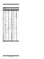
1
5066 User’s Manual Doc. #04497 Rev. 1003 OCTAGON SYSTEMS CORPORATION® 6510 W. 91st Ave. Westminster, CO 80030 Tech. Support: 303–426–4521 COPYRIGHT Copyright 1996, 1998, 2003—Octagon Systems Corporation. All rights reserved. However, any part of this document may be reproduced, provided that Octagon Systems Corporation is cited as the source. The contents of this manual and the specifications herein may change without notice. TRADEMARKS DiskOnChip® is a registered trademark of M-Systems. Micro PC, PC SmartLink, Octagon Systems Corporation®, the Octagon logo and the Micro PC logo are trademarks of Octagon Systems Corporation. QNX® is a registered trademark of QNX Software Systems, Ltd. QuickBASIC® is a registered trademark of Microsoft Corporation. ROM-DOS is a trademark of Datalight. PICO FA is a trademark of Phoenix Technologies, Ltd. NOTICE TO USER The information contained in this manual is believed to be correct. However, Octagon assumes no responsibility for any of the circuits described herein, conveys no license under any patent or other right, and makes no representations that the circuits are free from patent infringement. Octagon makes no representation or warranty that such applications will be suitable for the use specified without further testing or modification. Octagon Systems Corporation general policy does not recommend the use of its products in life support applications where the failure or malfunction of a component may directly threaten life or injury. It is a Condition of Sale that the user of Octagon products in life support applications assumes all the risk of such use and indemnifies Octagon against all damage. IMPORTANT! Please read before installing your product. Octagon's products are designed to be high in performance while consuming very little power. In order to maintain this advantage, CMOS circuitry is used. CMOS chips have specific needs and some special requirements that the user must be aware of. Read the following to help avoid damage to your card from the use of CMOS chips. Using CMOS Circuitry – 1 Using CMOS Circuitry in Industrial Control Industrial computers originally used LSTTL circuits. Because many PC components are used in laptop computers, IC manufacturers are exclusively using CMOS technology. Both TTL and CMOS have failure mechanisms, but they are different. This section describes some of the common failures which are common to all manufacturers of CMOS equipment. However, much of the information has been put in the context of the Micro PC. Octagon has developed a reliable database of customer-induced, field failures. The average MTBF of Micro PC cards exceeds 11 years, yet there are failures. Most failures have been identified as customer-induced, but there is a small percentage that cannot be identified. As expected, virtually all the failures occur when bringing up the first system. On subsequent systems, the failure rate drops dramatically. ■ Approximately 20% of the returned cards are problem-free. These cards, typically, have the wrong jumper settings or the customer has problems with the software. This causes frustration for the customer and incurs a testing charge from Octagon. ■ Of the remaining 80% of the cards, 90% of these cards fail due to customer misuse and accident. Customers often cannot pinpoint the cause of the misuse. ■ Therefore, 72% of the returned cards are damaged through some type of misuse. Of the remaining 8%, Octagon is unable to determine the cause of the failure and repairs these cards at no charge if they are under warranty. The most common failures on CPU cards are over voltage of the power supply, static discharge, and damage to the serial and parallel ports. On expansion cards, the most common failures are static discharge, over voltage of inputs, over current of outputs, and misuse of the CMOS circuitry with regards to power supply sequencing. In the case of the video cards, the most common failure is to miswire the card to the flat panel display. Miswiring can damage both the card and an expensive display. ■ Multiple component failures - The chance of a random component failure is very rare since the average MTBF of an Octagon card is greater than 11 years. In a 7 year study, Octagon has never found a single case where multiple IC Using CMOS Circuitry – 2 failures were not caused by misuse or accident. It is very probable that multiple component failures indicate that they were user-induced. ■ Testing “dead” cards - For a card that is “completely nonfunctional”, there is a simple test to determine accidental over voltage, reverse voltage or other “forced” current situations. Unplug the card from the bus and remove all cables. Using an ordinary digital ohmmeter on the 2,000 ohm scale, measure the resistance between power and ground. Record this number. Reverse the ohmmeter leads and measure the resistance again. If the ratio of the resistances is 2:1 or greater, fault conditions most likely have occurred. A common cause is miswiring the power supply. ■ Improper power causes catastrophic failure - If a card has had reverse polarity or high voltage applied, replacing a failed component is not an adequate fix. Other components probably have been partially damaged or a failure mechanism has been induced. Therefore, a failure will probably occur in the future. For such cards, Octagon highly recommends that these cards be replaced. ■ Other over-voltage symptoms - In over-voltage situations, the programmable logic devices, EPROMs and CPU chips, usually fail in this order. The failed device may be hot to the touch. It is usually the case that only one IC will be overheated at a time. ■ Power sequencing - The major failure of I/O chips is caused by the external application of input voltage while the Micro PC power is off. If you apply 5V to the input of a TTL chip with the power off, nothing will happen. Applying a 5V input to a CMOS card will cause the current to flow through the input and out the 5V power pin. This current attempts to power up the card. Most inputs are rated at 25 mA maximum. When this is exceeded, the chip may be damaged. ■ Failure on power-up - Even when there is not enough current to destroy an input described above, the chip may be destroyed when the power to the card is applied. This is due to the fact that the input current biases the IC so that it acts as a forward biased diode on power-up. This type of failure is typical on serial interface chips. ■ Serial and parallel - Customers sometimes connect the serial and printer devices to the Micro PC while the power is off. This Using CMOS Circuitry – 3 can cause the failure mentioned in the above section, Failure upon power-up. Even if they are connected with the Micro PC on, there can be another failure mechanism. Some serial and printer devices do not share the same power (AC) grounding. The leakage can cause the serial or parallel signals to be 20-40V above the Micro PC ground, thus, damaging the ports as they are plugged in. This would not be a problem if the ground pin is connected first, but there is no guarantee of this. Damage to the printer port chip will cause the serial ports to fail as they share the same chip. ■ Hot insertion - Plugging cards into the card cage with the power on will usually not cause a problem. (Octagon urges that you do not do this!) However, the card may be damaged if the right sequence of pins contacts as the card is pushed into the socket. This usually damages bus driver chips and they may become hot when the power is applied. This is one of the most common failures of expansion cards. ■ Using desktop PC power supplies - Occasionally, a customer will use a regular desktop PC power supply when bringing up a system. Most of these are rated at 5V at 20A or more. Switching supplies usually require a 20% load to operate properly. This means 4A or more. Since a typical Micro PC system takes less than 2A, the supply does not regulate properly. Customers have reported that the output can drift up to 7V and/or with 78V voltage spikes. Unless a scope is connected, you may not see these transients. ■ Terminated backplanes - Some customers try to use Micro PC cards in backplanes that have resistor/capacitor termination networks. CMOS cards cannot be used with termination networks. Generally, the cards will function erratically or the bus drivers may fail due to excessive output currents. ■ Excessive signal lead lengths - Another source of failure that was identified years ago at Octagon was excessive lead lengths on digital inputs. Long leads act as an antenna to pick up noise. They can also act as unterminated transmission lines. When 5V is switch onto a line, it creates a transient waveform. Octagon has seen submicrosecond pulses of 8V or more. The solution is to place a capacitor, for example 0.1 µF, across the switch contact. This will also eliminate radio frequency and other high frequency pickup. Using CMOS Circuitry – 4 Avoiding Damage to the Heatsink/CPU WARNING: When handling any Octagon CPU card, extreme care must be taken not to strike the heatsink against another object, such as a table edge. Also, be careful not to drop the CPU card, since this may cause damage to the heatsink/CPU as well. Epoxy adhesive bonds the heatsink to the CPU chip. When the heatsink is struck, the epoxy adhesive does not allow the heatsink to separate from the chip. The force of the blow to the heatsink then causes the legs of the CPU chip to separate from the PCB. This force damages both the CPU chip and the PCB. NOTE: Any physical damage to the CPU control card is not covered under warranty. Using CMOS Circuitry – 5 This page intentionally left blank. Using CMOS Circuitry – 6 TABLE OF CONTENTS COPYRIGHT ..................................................................... ii TRADEMARKS .................................................................. ii NOTICE TO USER ............................................................ ii IMPORTANT! ............................................... 1 TABLE OF CONTENTS ............................. iii 5066 CONVERSION SUMMARY ............... ix Solid State Disk Support ................................................... ix SSD1 ................................................................................... ix SSD0 ................................................................................... ix Setup Parameters ............................................................. ix Serial Ports ........................................................................ x Parallel Port ........................................................................ x Keyboard Connector .......................................................... x Speaker .............................................................................. x Battery ............................................................................... xi Power Management .......................................................... xi Current Requirements ....................................................... xi QNX Drivers ..................................................................... xi Memory Windows/Locations ............................................. xi PREFACE ..................................................... 1 Conventions Used in This Manual ...................................... 1 Symbols and Terminology .................................................. 2 Technical Support .............................................................. 4 CHAPTER 1: OVERVIEW........................... 5 Description ......................................................................... 5 Major Features ................................................................... 5 Where to go from here: ......................................................... 8 CHAPTER 2: QUICK START ................... 11 Hardware Installation ....................................................... 11 Using a Micro PC Card Cage .............................................. 12 Panel Mounting or Stacking the 5066 .................................. 15 Using the 5066 in a Passive Backplane .............................. 18 Establishing Communications with the 5066 .................... 20 Transferring Files between 5066 & Your PC ..................... 22 Downloading Files to the 5066 using TRANSFER.EXE ....... 23 Downloading Files to the 5066 using REMDISK/REMSERV ........................................................ 25 iii CHAPTER 3: SSDs, DRAM & BATTERY BACKUP ..................................................... 33 Description ....................................................................... 33 SSD0 ................................................................................ 33 SSD0 replaced with flash or SRAM .................................... 33 SSD0 replaced with another EPROM/OTROM .................... 35 SSD1 ................................................................................ 36 DRAM .............................................................................. 37 Battery Backup for SSD0 SRAM & Calendar Clock ........ 37 Using an AT battery ............................................................ 38 Using a DS-1213 Dallas module ......................................... 38 CHAPTER 4: SETUP PROGRAMS ......... 39 SETUP ............................................................................. 39 Running SETUP ................................................................. 41 SETUP Example .............................................................. 45 SETSSD .......................................................................... 46 PMISETUP ...................................................................... 48 CHAPTER 5: SAVE & RUN PROGRAMS49 Save and Run Your Programs on the 5066 ...................... 49 Saving Program and Support Files .................................. 49 Formatting SSD1 ................................................................ 49 Adding Operating System Startup Files (Using SYS) ......... 50 Adding Your Application ...................................................... 51 Autoexecuting Your Application ........................................... 52 Overriding the Autoexecution of Your Application ................ 52 CHAPTER 6: SERIAL PORTS ................. 55 Description ....................................................................... 55 COM1 as Console I/O...................................................... 56 COM1 as RS–232 I/O ...................................................... 57 COM2 as RS-485/RS-232 I/O ......................................... 57 RS-485 Transmitter Control .............................................. 59 Disabling Interrupts .......................................................... 60 Using QuickBASIC When No Video Card Present .......... 61 Systems with a video card ................................................. 61 Systems without a video card ............................................. 61 Using Turbo C ..................................................................... 63 iv CHAPTER 7: WATCHDOG TIMER, RESET & REMOTE SUSPEND/RESUME ............. 65 Watchdog Timer ............................................................... 65 Enhanced INT 17H Function Definitions .......................... 65 Enable Watchdog ................................................................ 65 Strobe Watchdog ................................................................ 66 Disable Watchdog ............................................................... 66 Hardware Reset ............................................................... 67 Remote Suspend/Resume Inputs .................................... 67 Example ............................................................................. 68 CHAPTER 8: LPT1 PARALLEL PORT ... 69 LPT1 Parallel Port ............................................................ 69 Printer ............................................................................... 69 Display ............................................................................. 70 Keypad ............................................................................. 71 Floppy Disk Drive ............................................................ 72 Opto Rack ........................................................................ 73 CHAPTER 9: SERIAL EEPROM & CMOS RAM ............................................................ 75 Description ....................................................................... 75 Enhanced INT 17H Function Definitions .......................... 75 Serial EEPROM ............................................................... 75 Read a Single Word from the Serial EEPROM .................... Write a Single Word to the Serial EEPROM ........................ Read Multiple Words from the Serial EEPROM ................... Write Multiple Words to the Serial EEPROM ....................... Return Serial EEPROM Size .............................................. 75 76 77 78 79 CMOS RAM ..................................................................... 80 Read Extended CMOS RAM ............................................... Write Extended CMOS RAM ............................................... Check CMOS Battery ......................................................... Copy Contents of Serial EEPROM to CMOS RAM ............. Copy Contents of Extended CMOS RAM to Serial EEPROM ........................................................................... 80 81 82 83 84 CHAPTER 10: VIDEO/KEYBOARD/ SPEAKER .................................................. 85 Description ....................................................................... 85 Using a Video Monitor and Keyboard ............................... 86 Saving a Program to the 5066 ............................................ 86 v Transferring Files to the 5066 .............................................. 86 Transferring Files from the 5066 .......................................... 88 Using REMDISK/REMSERV............................................... 89 CHAPTER 11: EXTERNAL DRIVES ....... 91 Description ....................................................................... 91 Floppy Disk Drives .......................................................... 91 Hard Disk Drive ............................................................... 92 CHAPTER 12: USER-DEFINED JUMPER ..................................................... 95 User-defined jumper ......................................................... 95 enhanced int 17h function definitions ............................... 95 Read jumpers ..................................................................... 95 CHAPTER 13: IRQ ROUTING & OPTO IRQs ............................................................ 97 Interrupt Routing Options ................................................. 97 Opto IRQ ............................................................................ 98 CHAPTER 14: LED SIGNALING ........... 101 Description ..................................................................... 101 CHAPTER 15: CPU POWER MANAGEMENT ....................................... 105 Description ..................................................................... 105 Power Management Overview ....................................... 105 Hardware Controlled Modes .......................................... 106 Device Power Management ........................................... 107 System Power Management .......................................... 108 How to Initiate the SUSPEND/RESUME Option ............... 109 How to Initiate the STANDBY Option ................................ 111 Save to Disk................................................................... 113 How to Initiate the Save to Disk Option ............................ 114 Power Management Configuration ................................. 115 Enabling Power Management ............................................ System Timers ................................................................. DOZE Timer Enable and Resets ....................................... IDLE Timer Resets ........................................................... RESUME from STANDBY ................................................. RESUME from SUSPEND ................................................ Power Failure - Save to Disk ............................................. Thermal Management ....................................................... vi 116 116 117 117 118 119 120 120 PMISETUP .................................................................... 122 CHAPTER 16: USING PICO FA ............. 129 Description ..................................................................... 129 Using PFORMAT ........................................................... 129 Using TESTRFA ............................................................. 130 Making Copies of SSD1's Contents for Other Boards ....... 130 CHAPTER 17: TROUBLESHOOTING ... 133 No Screen Activity – Checking Console Serial Communications ............................................................... Garbled Console Screen Activity ...................................... System generates a BIOS message but locks up when booting from SSD1: .......................................................... PICO FA reports a drive, but issuing a DIR generates an error message. ............................................................. PICO FA does not report the drive. ................................... System will not recognize hard drive. ............................... System locks up on power up; may or may not respond to reset switch. ................................................................. System locks up after power down/power up. ................... 133 133 134 134 134 134 135 135 Technical Assistance ..................................................... 135 CHAPTER 18: TECHNICAL DATA......... 137 Technical Specifications ................................................. 137 Jumper Settings ............................................................. 142 Connector Pinouts ......................................................... 146 micro pc bus pinouts ...................................................... 151 Introduction .................................................................... 153 Support commands: ......................................................... 153 Support device drivers: ..................................................... 153 APPENDIX A: SOFTWARE UTILITIES . 153 GETBIOS.EXE ................................................................. GETIMG.EXE .................................................................. GETIMGH.EXE ................................................................ HIMEM.SY ....................................................................... I17HNDLR.EXE ................................................................ LPT1CON.COM ................................................................ PFORMAT.EXE ................................................................ PGMBIOS.EXE ................................................................ PGMIMG.EXE .................................................................. PGMIMGH.EXE ............................................................... vii 154 155 156 158 160 161 162 163 164 165 PHDISK.EXE ................................................................... PICOFA.SYS .................................................................... PMISETUP.EXE ............................................................... REMDISK.EXE ................................................................ REMQUIT.COM ................................................................ REMSERV.EXE ................................................................ RESET.COM .................................................................... SCONSOLE.EXE ............................................................. SERACON.EXE ............................................................... SETSSD.EXE .................................................................. SETUP.COM .................................................................... TESTRFA.EXE ................................................................. TRANSFER.EXE .............................................................. VDISK.SYS ...................................................................... 166 168 169 170 173 174 176 177 178 179 182 184 185 188 APPENDIX B: TIPS ................................. 191 Custom Communication Cable ...................................... 191 Power Supply ................................................................. 192 Uploading Files from the 5066 ........................................ 192 APPENDIX C: THIRD PARTY SUPPORT ................................................ 195 Using QNX on the 5066 ................................................. 195 Programming QNX into SSD1 ........................................... 195 Using M-Systems DiskOnChip (DOC) .......................... 195 WARRANTY ............................................. 189 LIMITATIONS ON WARRANTY ......................................... SERVICE POLICY ............................................................ RETURNING A PRODUCT FOR REPAIR ......................... RETURNS ........................................................................ GOVERNING LAW............................................................ viii 189 189 190 190 190 5066 CONVERSION SUMMARY The 5066 CPU card is designed to provide customers with an easy upgrade path from the 5025 and 5025A cards. There are some differences that you may need to know about when converting your 5025/5025A applications to the 5066. This section outlines those differences. This information is provided in greater detail in the following chapters of this manual. If you need further assistance, call Octagon Technical Support Department at (303) 426-4521. SOLID STATE DISK SUPPORT SSD1 A 2 MB flash EPROM is surface-mounted in SSD1. This eliminates the need to purchase a separate flash EPROM. Your application program, CONFIG.SYS, AUTOEXEC.BAT, and any other required support files may be placed in SSD1 (128K of SSD1 is reserved for system use). SSD1 contains additional utilities such as a flash file system which gives you read/write capability. Hence, you will not need to use an SRAM to give you file write capabilities during run time. However, the flash devices do have limited write cycle capabilities (approximately 100,000 write cycles). SSD0 As shipped from the factory, the SSD0 socket contains a 512K EPROM with BIOS, DOS, and various other utilities programmed into it. This is the default boot drive. You may configure this socket with a battery-backed SRAM (up to 512K) for applications that perform contstant file writes (e.g., data logging). When using an SRAM in SSD0, we highly recommend that you configure the 5066 to boot from the flash device (SSD1). SETUP PARAMETERS The 5066 has a setup program utility that is very similar to that of the 5025/5025A products. Setup information is stored in a 2048 byte serial EEPROM. A total of 1536 bytes of storage area is available for your use. (This is slightly less that what is available on the 5025A.) ix SERIAL PORTS Both of the 5066 RS-232 serial ports are identical to those on the 5025/5025A, and they feature 16 byte FIFO buffers with advanced hardware protection. The RS-485 implementation and termination on the 5066 differs from the 5025/5025A products. In addition, the 5066 does not directly support four-wire mode. If you need to use four-wire mode, use Octagon's MTB-485 converter (Order# 2894). PARALLEL PORT The 5066 LPT1 parallel port has been greatly enhanced over the 5025/5025A products. This port supports IEEE 1284 EPP and ECP modes, and has backdrive protection. Moreover, this port can be used to interface with a floppy disk drive. The port is terminated in a 26-pin IDC connector. (The 5025/5025A products use a 20-pin IDC connector.) Use Octagon’s VTC-5 cable (Order# 1237) to interface this port with a printer. The LCD-IFB and DP-IFB display/keypad boards are not directly compatible with this 26-pin port. If you need to interface with Octagon’s LCD displays or keypads, use the 2010 interface card (Order# 3909) and a CMA-26 style cable. KEYBOARD CONNECTOR You may plug a PS-2 style keyboard directly into the 5066. The 5066 contains a 6-pin mini-DIN PS-2 style connector. Unlike the 5025/5025A products, you will not need to purchase the PSKI-1 interface board to connect to a keyboard. SPEAKER Unlike the speaker interface on the 5025/5025A products, the 5066 speaker interface is a stand-alone, 3-pin header. x BATTERY The 5066 uses the same style battery connector as on the 5025/ 5025A products. The real time clock can be battery-backed using a standard “AT-style” battery (Order# 3186). If an SRAM is installed in SSD0, SSD0 can be battery-backed also. POWER MANAGEMENT The 5025/5025A products have very little power management utilities. The 5066 has advanced power management capabilities. Options and implementation details are listed in this manual. CURRENT REQUIREMENTS The 5066 draws a maximum of 1.21A (5 VDC) with 1 MB of DRAM at full speed (5x86 processor). Current consumption can be reduced by as much as 75% by implementing the advanced power management functions. QNX DRIVERS QNX SSD drivers for the 5025A will not work on the 5066. QNX has developed SSD drivers for the 5066. For more information on using the QNX software with SSD1, refer to the QNX SSD support utility disk (P/N 4870) . MEMORY WINDOWS/LOCATIONS The following memory locations are reserved on the 5066: D8000-E0000 E0000-E8000 E8000-F0000 F0000-FFFFF PICO FA and other system utilities Advanced Power Management Window for SSD bank switching BIOS xi This page intentionally left blank. xii PREFACE This manual provides all the information required to install, configure, and operate the 5066 Micro PC Control Card. It is part of Octagon’s Micro PC user manual series. To receive the Micro PC User Manual Binder, please return the reply card included with your Control Card. By using this manual, you will be able to: • Interface the 5066 Control Card to your PC and the Micro PC expansion cards. • Set up communications between the 5066 card and a PC. • Gain an understanding of the operation and various options allowed in the 5066 Control Card. CONVENTIONS USED IN THIS MANUAL 1. Information which appears on your screen is shown in a different type face, for example: PhoenixBIOS(TM) A486 Version 1.03 Copyright (C) 1985-1994 Phoenix Technologies, Ltd. All Rights Reserved Octagon Systems Corp. 5066 CPU 2. Commands that you must key in are shown in Courier Bold, for example: C:> RESET 3. Italicized refers to information that is specific to your particular system or program, e.g., Enter filename means enter the name of your file. 4. Warnings always appear in this format: WARNING: The warning message appears here. 5. Paired angle brackets are used to indicate a specific key on your keyboard, e.g., <ESC> means the escape key; <CTRL> means the control key; <F1> means the F1 function key. 6. All addresses are given in hexadecimal. Preface – 1 SYMBOLS AND TERMINOLOGY Throughout this manual, the following symbols and terminology are used: W[ – ] Denotes a jumper block and the pins to connect. Autoexecution Automatic execution of a program on power– up or reset. BIOS drive The solid–state disk which contains the system BIOS and ROM–DOS. Console Port Video card or COM1 where BIOS and DOS messages appear and keyboard input is available. Control Card Contains the CPU, memory, and operating system and controls the operation of all the extension cards. DRAM Dynamic Random Access Memory devices. DRAMs provide volatile memory with unlimited read and write cycles. Expansion Card The expansion cards add I/O functions to the Micro PC system, such as analog input/ output, digital input/output, motion control, display, and so on. Flash memory Electrically erasable PROM which allows at least 100,000 write cycles. Memory device The type of static RAM, DRAM, flash memory or EPROM specified for either volatile or nonvolatile memory. PC SmartLINK A serial communications software package designed by Octagon for use with the 5066 Control Card. Refers to all versions of PC SmartLINK. Preface – 2 ROM Read Only Memory devices. ROMs provide nonvolatile memory, have a limited number of write cycles, and include EPROMs, EEPROMs, and flash memory. ROM–DOS Operating system included in Micro PC ROM. Solid–State Disk (SSD) A simulated disk using a high speed solid– state memory device, for example flash memory, EEPROM, or static RAM. Static RAM Static Random Access Memory device. Static RAMs provide volatile memory with unlimited read and write cycles. They may be used with a back–up battery. TTL Compatible Transistor transistor logic compatible; 0–5V logic levels. Virtual Drive A disk created in DOS or extended memory which emulates an actual disk. Provides temporary storage for files. When power to the computer is turned off the virtual drive disappears. XMODEM A communications protocol which allows transfer of files between two computers. XON/XOFF A communications protocol for asynchronous connections. The receiver can pace the sender by sending the XOFF and XON characters to stop and continue the data flow. H The suffix “H” denotes a hexadecimal number. A decimal number has no prefix or suffix. For example, 1000H and 4096 are equivalent. Preface – 3 TECHNICAL SUPPORT If you have a question about the 5066 Control Card and cannot find the answer in this manual, call Technical Support. They will be ready to give you the assistance you need. When you call, please have the following at hand: Your 5066 Control Card User’s Manual A description of your problem. The direct line to Technical Support is 303–426–4521 and the e–mail address is [email protected]. Preface – 4 CHAPTER 1: OVERVIEW DESCRIPTION The 5066 is intended for high performance, embedded control applications. Despite its small size, the features include: a 133 MHz 5x86 processor; Datalight ROM-DOS 6.22 in ROM; two serial ports, including one RS-485 port; a multifunctional parallel port; a watchdog timer; up to 8 MB of on–card DRAM; a DIMM socket for up to an additional 32 MB of memory; 2 MB of flash memory with an integral programmer, 512K socket for EPROM, flash or SRAM; keyboard and speaker ports; two solid–state disks; an 8bit ISA Bus interface; power management utilities; flexible interrupt routing; user option jumper; visual LED signaling; and opto-isolated interrupts. In addition, flash can be programmed oncard. The card can be used in a stand–alone mode or installed in a passive ISA Bus backplane. The 5066 can also be installed in a card cage. MAJOR FEATURES Instant DOS The 5066 is an “instant DOS” system. The card includes Datalight ROM-DOS 6.22 compatible DOS in a solid–state disk. The system boots and operates the same way as your desktop PC. Watchdog Timer The watchdog timer resets the system if the program stops unexpectedly. The watchdog is enabled, disabled and strobed under software control. The timeout is 1.6 seconds (1.6 sec. typical, 1.00 sec. min., 2.25 sec. max.). Calendar/Clock The 5066 has a built–in, AT style calendar/clock. An external AT clock battery plugs into the card and powers the clock during power–down. The battery is not required for normal system setup information. The calendar/clock also provides the user with 128 bytes of user-defined CMOS RAM. Overview – 5 Solid–State Disk Options SSD0 contains the BIOS drive and ROM-DOS 6.22 in ROM. It reserves 128K for BIOS and 384K for a drive area. SSD0 options include: 512K 5V flash 512K EPROM/OTPROM 512K SRAM NOTE: A DOS-compatible read/write drive is built-in when using a flash device or SRAM in SSD0. NOTE: When using the 512K SRAM option, the 5066 requires battery back-up. Static RAM contents are sometimes affected by system noise. Therefore, the use of static RAM is not recommended in electrically noisy environments, especially when systems are critical. SSD1 is used for storage of the applications program. A 2 MB 5V flash is soldered on card. The flash memory programmer is built–in allowing the device to function as a read/write solid state disk drive. SSD1 is described in further detail in the RAMs and EPROMs chapter. SSD1 reserves 128K for BIOS and 896K for a drive area. Speaker and Keyboard Port The 5066 accepts AT keyboard input and has the PS–2 style keyboard connector. The speaker port is a 3–pin connector for use with any external speaker from 8–50 ohms. See the Video/ Keyboard/Speaker chapter for pinouts. Power Management The 5066 includes power management utilities, that can be enabled in the SETUP program, and are adjusted with the PMISETUP program. DOS-supplied programs such as POWER.EXE are also supported. See the utility disk for a list of example programs. Overview – 6 Mounting There are several ways to mount the 5066: 1. Plug it directly into an 8-bit Micro PC card cage. 2. Use the optional PC mounting bracket and plug it into any passive backplane. 3. Panel mount it using the four mounting holes. A screw terminal connector is used to supply the 5V power. 4. Stack it with other Micro PC cards. Serial Ports COM1 and COM2 are 16C550 compatible. The baud rates are programmable from 150 to 115K baud. Both ports have a RS–232 interface. RS–232 voltages are generated on–card. COM2 is also configurable as RS–485 for multidrop operation. LPT1 Multifunctional Parallel Port The LPT1 multifunctional parallel port can be used for a printer port, for general purpose I/O, or for interfacing with a floppy disk drive. For embedded applications, an interface board and software are available to interface with a 4–line LCD display and a 16–position keypad. The port can also be connected to the MPB–16PC, a 16–position opto module rack for driving high current AC and DC loads. The parallel port also has unidirectional mode, bidirectional mode, enhanced parallel port (EPP) mode, and extended capabilities port (ECP) mode. Setup stored in serial EEPROM The 5066 stores the setup information in nonvolatile EEPROM; as a result it is immune to battery or power failure (with the exception of time and date). 512 bytes of the serial EEPROM is reserved by the BIOS. The user can store up to 1,536 bytes of information in the remainder of the EEPROM. Overview – 7 Hardware Reset A hardware reset can be done by any of the following means: issuing the RESET software command (using the watchdog function); cycling power; or depressing the reset switch. A hardware reset ensures complete reset of the system and all attached peripherals. An expired watchdog timer cycle also causes a hardware reset to occur. Boot sequence A system can be configured to boot from the oncard solid–state disk, or an external floppy or hard disk. Where to go from here: Before you begin developing your application program for the 5066, we recommend you read Chapters 2–4. These chapters give instructions for hardware installation, downloading and saving your program, and autoexecuting your application. Chapter 2 Quick Start Covers the basics of setting up a 5066 system. This chapter describes how to install the 5066 into the card cage, how to establish a serial communications link with your PC and how to download files to the 5066. Chapter 3 SSDs, DRAM & Battery Backup Configuring and installing EPROMs. Installing the battery backup and calendar clock. This chapter also includes a description about the DRAM on the 5066. Chapter 4 Setup Programs Running the SETUP configuration program, the SETSSD program, and the PMISETUP program. Chapter 5 Save & Run Programs How to save your program files and autoexecute them from the 5066. This chapter also discusses how to use your own DOS O/S. Chapter 6 Using COM1 and COM2. Setting Overview – 8 Serial Ports COM1 as the main console I/O for serial communications with your PC and setting COM2 for RS-485 operation. Chapter 7 Watchdog Timer, Reset & Remote Suspend/Resume Enabling the watchdog timer, system reset, and remote suspend/resume. Chapter 8 LPT1 Parallel Port Using the multifunctional parallel port for a printer, display, keypad, opto rack, floppy disk or other device. Chapter 9 Serial EEPROM & CMOS RAM How to read and write to the serial EEPROM and using CMOS RAM. Chapter 10 Video/Keyboard/Speaker Configuring the 5066 with a video, keyboard and speaker. Chapter 11 External Drives Configuring the 5066 with a floppy drive or hard drive. Chapter 12 User-defined Jumper Reading the user-defined jumper by code in your program. Chapter 13 IRQ Routing & Opto IRQs Configuring the IRQs for maximum connectivity and opto IRQ. Chapter 14 LED Signaling Using the bi-color LED to provide system status signaling. Chapter 15 CPU Power Management Using the built-in power management utilities. Chapter 16 Using PICO FA Using the PICO FA utility program. Overview – 9 Chapter 17 Troubleshooting Problems encountered when using the 5066. Chapter 18 Technical Data Technical specifications, jumper configurations and connector pinouts. Appendix A Software Utilities Description and operation of software utility programs and device drivers. Appendix B Tips Using non–Octagon cables and uploading files from the 5066. Appendix C Third Party Support Using QNX and M–Systems DiskOnChip Overview – 10 CHAPTER 2: QUICK START This chapter covers the basics of setting up a 5066 system and tells you: 1. How to panel mount, stack or install the 5066 into the card cage; 2. How to set up a serial communications link between the 5066 and your PC; and 3. How to download files to the 5066 and run a program from the virtual drive. WARNING: The 5066 may not be installed in a PC. These cards are designed to be independent CPU cards only, not accelerators or coprocessors. HARDWARE INSTALLATION Your 5066 Control Card can be installed in one of several ways: 1. Plug it directly into a 8-bit Micro PC card cage; 2. Use the optional PC mounting bracket and plug it into any 8-bit passive backplane; 3. Panel mount it using the four mounting holes; 4. Stack it with other Micro PC cards. Figure 2-1 provides a component diagram of the 5066. Refer to it as needed. Quick Start – 11 IRQ Routing Option Speaker Battery W5 LED Power Indicator IRQ Routing Option U9 U8 U7 J7 U6 J1 J6 Keyboard COM1 W1 J2 W6 COM2 Type Select COM2 J3 W3 W2 U15 U15 SSD0/BIOS J4 W4 +5V Power P2 U13 J5 LPT1 Opto IRQ/ Power Mngmnt/ Suspend Resume Gnd SSD0 Type Select Boot Select User Option Panel Mounting Holes (4) = Pin 1 Figure 2-1 – 5066 Component Diagram Using a Micro PC Card Cage To install the 5066 in a Micro PC card cage, you will need the following equipment (or equivalent): 5066 Control Card Micro PC Card Cage (5xxx Card Cage) Power Module (510x or 71xx Power Module) VTC–9F Cable Null modem adapter 5066 ROM–DOS & Utility Software Disk PC SmartLINK with manual Your PC Please refer to Appendix B if you are making your own serial cable or using other non–Octagon components. Quick Start – 12 To install the 5066: 1. Refer to Figure 2-1 for the location of various connectors before installing the 5066 Control Card. WARNING: The 5066 Control Card contains static–sensitive CMOS components. The card is most susceptible to damage when it is plugged into a card cage. The 5066 card becomes charged by the user, and the static discharges to the backplane from the pin closest to the card connector. If that pin happens to be an input pin, even TTL inputs may be damaged. To avoid damaging your card and its components: • • • WARNING: Ground yourself before handling the 5066 card. Disconnect power before removing or inserting the card. When programming a memory device, place the device in the socket before applying power. Take care to correctly position the 5066 card in the card cage. The VCC and ground signals must match those on the backplane. Figure 2-2 shows the relative positions of the 5066 card as it is installed in the card cage. A31 B31 Micro-PC Passive Backplane Card Edge Pins A31 & B31 5066 Control Card A1 B1 Card Edge Pins A1 & B1 Figure 2-2 – Edge Connector Orientation Quick Start – 13 2. Attach the power module to the card cage following the instructions supplied with the power module. 3. Make sure power to the card cage is OFF. 4. Slide the 5066 into the card cage. The ROM–BIOS label on the card should face to the left. See Figure 2-3 for an illustration of the 5066 in a Micro PC card cage. Figure 2-3 — Populated Micro PC Card Cage WARNING: 5. Plugging the card in incorrectly will destroy the card! Connect one end of a VTC–9F cable to the null modem adapter. Connect the other end to COM1 (J2) on the 5066. NOTE: You must use COM1 on the 5066 in order to establish a serial communications link with your PC. 6. If your PC has a 9–pin serial connector, connect the null modem adapter to any serial port (COM1 – COM4) on your PC. If your PC has a 25–pin serial connector, attach a 9– to 25–pin adapter to your null modem adapter, then insert the matching end of the 9– to 25–pin adapter into the serial port. See Figure 2-4. Quick Start – 14 DB-9 Connectors Desktop PC COM1 9F VTC- ble Ca COM Port Null Modem Adapter Octagon Control Card OR DB-9 to DB-25 Adapter Desktop PC 9 VTC- e abl FC COM Port Null Modem Adapter DB-25 Connector Figure 2-4 – Serial Communications Setup NOTE: Please refer to the PC SmartLINK manual for more information on using a COM port other than COM1. You are now ready to transfer files between your PC and the 5066. Please continue with the section, “Establishing Communications with the 5066,” in this chapter. Panel Mounting or Stacking the 5066 To panel mount or stack the 5066, you will need the following equipment (or equivalent): 5066 Control Card 5V Power Supply VTC–9F Cable Null modem adapter 5066 ROM–DOS & Utility Software Disk PC SmartLINK with manual Your PC 5252MB Stacking Kit (required for stacking only) (P/N 3590) Please refer to Appendix B if you are making your own serial cable or using other non–Octagon components. Quick Start – 15 If you are panel mounting the 5066, a screw terminal connector (P2) is provided to supply the 5V power. Refer to Figure 2-5 for an illustration of panel mounting the 5066. Refer to Figure 2-6 for an illustration of stacking the 5066 with the 5252MB Stacking Kit. WARNING: Miswiring the voltage at P2 of the 5066 or at the power connector of the 5252MB stacking kit (reversing +5V and ground, or applying a voltage greater than +5V), will destroy the card and void the warranty! Power connector (P2) Figure 2-5 — Panel Mounting the 5066 Power connector 5252MB stacking kit Figure 2-6 — Stacking the 5066 1. To panel mount the 5066, use #4–40 standoffs and screws to bolt down the card. The following diagram shows the center to center mounting hole dimensions. Quick Start – 16 To stack the 5066, refer to the 5252MB Stacking Kit Product Sheet enclosed with the kit. The proceed with Step 2 in this section. A B A = 4.90 in. (124,46 mm) B = 0.20 in. (5,08 mm) C = 3.50 in. (88,90 mm) D = 0.10 in. at 45°, 2 PLCS (2,54 mm at 45°) E = 0.475 in. (4,44 mm) F = 0.85 in. (21,59 mm) G = 3.20 in. (81,28 mm) H = 0.30 in. (7,62 mm) J = 4.20 in. (106,68 mm) J K = 0.20 in. (5,08 mm) 0.125 in. HOLE (3,17 mm) 4 PLCS C 0.015 in. at 45• CHAMFER, 2 PLCS (0,038 mm) A31 A1 H K F G F E D BEVEL CARD EDGE, 2 PLCS .015 in. x 45• (0,038 mm x 45•) Figure 2-7 — 5066 Center to Center Hole Dimensions 2. Connect the proper ground and 5V wires to the terminal block at P2. 3. Connect one end of the VTC–9F cable to the null modem adapter. Connect the other end to COM1 (J2) on the 5066. NOTE: You must use COM1 on the 5066 in order to establish a serial communications link with your PC. 4. If your PC has a 9–pin serial connector, connect the null modem adapter to any serial port (COM1 – COM4) on your PC. If your PC has a 25–pin serial connector, attach a 9–to 25–pin adapter to your null modem adapter, then insert the matching end of the 9– to 25–pin adapter into the serial port. See Figure 2-4. NOTE: Please refer to the PC SmartLINK manual for more information on using a COM port other than COM1. Quick Start – 17 You are now ready to transfer files between your PC and the 5066, please continue with the section, “Establishing Communications with the 5066” in this chapter. Using the 5066 in a Passive Backplane To plug the 5066 into a passive backplane, you will need the following equipment (or equivalent): 5066 Control Card Micro PC Backplane (52xx-BP) Mounting Bracket (optional) Power Module (510x Power Module) VTC–9F Cable Null modem adapter 5066 ROM–DOS & Utility Software Disk PC SmartLINK with manual Your PC Please refer to Appendix B if you are making your own serial cable or using other non–Octagon components. To install the 5066: 1. Make sure power to the backplane is OFF. 2. Insert the 5066 into a connector on the backplane. Take care to correctly position the card’s edge with the connector of the backplane. Figure 2-2 shows the relative positions of the 5066 card as it is installed into a backplane. WARNING: 3. Plugging the card in incorrectly will destroy the card and void the warranty! Place the backplane on a flat surface so that the card is in an upright position. With the top of the card and its components facing left, attach the mounting bracket (optional) onto the edge nearest you. Secure the mounting bracket with the two screws provided in the kit. See Figure 2-8. Quick Start – 18 Mounting bracket XT/AT passive backplane Figure 2-8 – Using a Passive Backplane 4. Connect one end of a VTC–9F cable to the null modem adapter. Connect the other end to COM1 (J2) on the 5066. NOTE: You must use COM1 on the 5066 in order to establish a serial communications link with your PC. 5. If your PC has a 9–pin serial connector, connect the null modem adapter to any serial port (COM1 – COM4) on your PC. If your PC has a 25–pin serial connector, attach a 9– to 25–pin adapter to your null modem adapter, then insert the matching end of the 9– to 25–pin adapter into the serial port. See Figure 2-4. NOTE: Please refer to the PC SmartLINK manual for more information on using a COM port other than COM1. You are now ready to transfer files between your PC and the 5066, please continue with the section, “Establishing Communications with the 5066” in this chapter. Quick Start – 19 ESTABLISHING COMMUNICATIONS WITH THE 5066 1. Install PC SmartLINK (or other communications software) on your PC if you have not already done so. Refer to the PC SmartLINK manual for installation instructions. 2. Copy the 5066 files from the 5066 utility disk to a subdirectory on your PC hard drive. C: MD C:\MPC XCOPY A:\*.* C:\MPC /S 3. Start PC SmartLINK. You are now ready to establish communications between your PC and the 5066 Control Card. 4. Power on the 5066. 5. A logon message similar to the one below will appear on your PC monitor: PhoenixBIOS(TM) A486 Version x.xx Copyright (C) 1985-1994 Phoenix Technologies, Ltd. All Rights Reserved Octagon Systems Corp. 5066 CPU 5066 BIOS vx.xx - mm/dd/yy Am5x86-WB processor detected operating at 133 Mhz 640K Base Memory, 07168K Extended On board memory configured as EDO DRAM INT 17h BIOS extension vx.xx Copyright (c) 1995-96 Octagon Systems Corporation PICO Flash Array Copyright (c) 1996, Phoenix Technologies Ltd. Resident Flash Array (RFA) OEM Layer Phoenix PICO Flash Array(TM) Copyright (c) 1996, Phoenix Technologies Ltd. Octagon Systems vx.xx First drive is in SSD0 (384K) Second drive is in SSD1 (896K) Starting ROM-DOS... Quick Start – 20 HIMEM v6.22 (Revision x.xx) Copyright (c) 1989-1995 Datalight, Inc. VDISK v6.22 (Revision x.xx) Copyright (c) 1989-1995 Datalight, Inc. Extended Memory Present VDISK v6.22 (Revision x.xx) Copyright (c) 1989-1995 Datalight, Inc. Formatting 2304K XMS memory as drive E: 5066 C:\> If you do not get the proper logon message: • Check the serial parameters of your PC to make sure they are set correctly. Parameters should be 9600 baud, 8 data bits, no parity, and 1 stop bit. • Make sure a video card is not installed in the card cage. • Make sure all jumpers are set to factory defaults. • If the system still does not respond, refer to the Troubleshooting chapter. 6. Use the directory command to make sure your equipment and software are working properly. Enter: 5066 C:\> DIR A directory listing of ROM–DOS files stored in the BIOS socket should appear: Volume in drive C is SSD0 Volume Serial Number is 3214-1BE4 Directory of C:\ COMMAND CONFIG AUTOEXEC DOS UTILS 7. COM 26,321 SYS 67 BAT 38 <DIR> <DIR> 5 file(s) 04–17–95 6:22a 04-12-96 8:26p 04-12-96 8:26p 04-12-96 8:26p 04-12-96 8:26p 26,426 bytes 105,472 bytes free You are now ready to transfer files between your PC and the 5066. Quick Start – 21 TRANSFERRING FILES BETWEEN 5066 & YOUR PC Once you have established communications between your PC and the 5066, you can serially download files to any read/write drive used by the 5066. You can then test and debug your application files before permanently saving them to flash or EPROM. You can also upload files from the 5066 to your desktop PC for editing and debugging. When booting from the 5066 BIOS drive, the default CONFIG.SYS device drivers designate drive C: as the BIOS drive (SSD0), drive D: as the flash drive (SSD1), and drive E: as the virtual drive. All drives assigned, except for drive C: (which is an EPROM), can be accessed as read/write drives and files can be serially transferred to and stored on any of these drives. NOTE: The SSD device drivers are optional when booting from SSD1, floppy or hard drive. For example, if you do not need a virtual drive, do not use VDISK.SYS. There are two methods to download files through the serial port to the 5066: 1. The TRANSFER utility is used to download files, one at a time, to the 5066 using the XMODEM protocol. TRANSFER.EXE resides on the 5066 BIOS drive and on the 5066 utility diskette and is used to send or receive files via the serial port (e.g., COM1). TRANSFER.EXE uses the XMODEM protocol, as does PC SmartLINK. (See the note below on XMODEM). 2. REMDISK/REMSERV utilities allow access to all of the files on a remote disk drive. REMDISK.EXE and REMSERV.EXE are located on the 5066 BIOS drive and the 5066 utility diskette. Once these programs are executed, single or multiple files can then be transferred to and from the 5066 using DOS COPY or XCOPY commands. TRANSFER.EXE, REMDISK.EXE and REMSERV.EXE are located on the 5066 BIOS drive, in the DOS directory, and on the 5066 utility diskette in the \DOS directory. Refer to Appendix A for more information on these programs. NOTE: XMODEM only transfers files in which the file size is exactly on a 128 byte boundary. If the file size does not fall exactly on the boundary, XMODEM automatically rounds the file size up to the next 128 byte boundary with padding characters. For example, a Quick Start – 22 file with a size of 10,000 bytes, will be rounded up to 10,112 bytes, transferred, and written with the new file size. In most cases, this is not a concern, but in some instances the XMODEM padding causes problems. The padding problems become apparent when an application program is expecting a specific file size or is expecting characters other than the padding characters to be at the end of the file. The following information on downloading files between the 5066 and your PC uses the example program DEMO.EXE. This file is on the 5066 utility diskette in the \DEMO directory. Downloading Files to the 5066 using TRANSFER.EXE The following procedures assume you are using PC SmartLINK and that it is included in your directory path. For other communication programs, refer to those programs instructions on sending a file from your PC to a target system. Refer to Appendix A for specific information on using TRANSFER.EXE. Hardware and software requirements: • Desktop PC, running PC SmartLINK, connected by a VTC-9F cable and a null modem adapter to COM1 of the 5066. • A 5066 running TRANSFER.EXE out of COM1. Connect the equipment as per the following diagram: PC SmartLINK 5066 TRANSFER.EXE VTC-9F Cable Desktop PC COM1 1. COM Port Null Modem Adapter Figure 2-9 – Downloading Files Using TRANSFER.EXE Quick Start – 23 2. On the PC, log into the directory which contains the file(s) you will download to the 5066, for example: C:\MPC\5066\DEMO 3. Start PC SmartLINK and power on the 5066. 4. Execute the TRANSFER.EXE program from the 5066 by entering: 5066 C:\> TRANSFER E:DEMO.EXE NOTE: In this case, E: is the virtual drive assigned in CONFIG.SYS. Any 5066 read/write drive could be substituted. The following message is displayed from the 5066: Receiving D:DEMO.EXE . . . 5. Execute the following steps using PC SmartLINK: a. b. c. d. Press <ALT><D> to enter the download screen. Type in the name of the file to transfer, e.g. DEMO.EXE (if PC SmartLINK was not started in the DEMO directory as instructed in Step 1, then the entire path may have to be entered C:\MPC\DEMO\DEMO.EXE) To begin the transfer: • either press ENTER (default download START); • tab to START; • click on the START button in the download screen. When the file transfer is completed, press <ESC> twice to return to the main PC SmartLINK screen. NOTE: TRANSFER.EXE will time-out if the program has not been started after approximately 40 seconds. If the time-out occurs, the following message from the 5066 is displayed: Failed to receive E:DEMO.EXE! Deleting E:DEMO.EXE Quick Start – 24 6. When the file transfer is complete, type the following DOS command to view the E: drive directory and confirm that your file has been transferred to the 5066: 5066 C:\> DIR E: The system will display the contents of drive E: Volume in drive E is VDISK vX.XX Directory of E:\ DEMO 7. EXE 1 file(s) 27264 06-07-96 27264 bytes 2:57p To execute the program you have just downloaded type: 5066 C:\> E:DEMO The DEMO program displays a message on your PC. Downloading Files to the 5066 using REMDISK/REMSERV There are three methods of using REMDISK/REMSERV with a 5066: 1. 2. 3. 5066 with no video card, one serial cable 5066 with no video card, two PCs, two serial cables 5066 with a 5420 video card, one serial cable Refer to Appendix A for specific information on using REMDISK.EXE and REMSERV.EXE. 5066 with no video card, one serial cable Hardware and software requirements: • Desktop PC, running REMDISK, connected by a VTC-9F cable and a null modem adapter to COM1 or COM2 of the 5066. • A 5066 running REMSERV out of COM1 or COM2. NOTE: COM2 is default configured for RS-485. Jumpers W1[56][7-8][9-10] must be changed to W1[1-3][2-4] to configure COM2 as RS-232. 1. Connect the equipment and load appropriate software on each system as per the following diagram: Quick Start – 25 REMDISK.EXE 5066 VTC-9F Cable Desktop PC COM1 REMSERV.EXE COM Port Null Modem Adapter Figure 2-10 – Downloading Files to 5066 with No Video Card Using REMDISK/REMSERV 2. On the PC, start PC SmartLINK from the C:\MPC\5066\DOS directory and power on the 5066. 3. Execute REMSERV.EXE on the 5066. Read/write SSD flash drive D: is the shared drive and COM1 is the default port. COM2 can be selected and the serial cable swapped to the COM2 header after REMSERV has been started. Enter: 5066 C:\> REMSERV D: The following message is displayed from the 5066: REMSERV v1.0 Copyright (c) 1990-1994 Datalight, Inc. All rights reserved. Using COM1 at 115K+ baud. Accessing Drive D: Time-out is 2 seconds Press <Esc> to Exit. (There may be a delay before exit occurs) 4. Exit PC SmartLINK by pressing <ALT><X>. 5. Execute REMDISK.EXE on the PC, by entering: Quick Start – 26 C:\> REMDISK The following message is displayed on the PC: Remote Disk v1.0 Copyright (c) 1990-1994 Datalight, Inc. All rights reserved. Installed as Drive E: /COM1 /B115+ /T10 NOTE: REMDISK assigns the remote drive as the last drive in the system. In this case, drive E: was assigned. 6. Files are transferred to the 5066 read/write drives by using the DOS COPY and XCOPY commands. Enter: C:\> COPY C:\MPC\5066\DEMO.EXE E: C:\> DIR E: C:\> E:DEMO.EXE The DEMO program displays a message on your PC. In this case, drive E: is the remote read/write SSD flash disk drive of the 5066. Files are easily copied between the drives. 7. When finished, execute: C:\> REMDISK /U This unloads REMDISK from the desktop PC. 8. Restart PC SmartLINK and reset the 5066. 5066 with no video card, two PCs, two serial cables The first desktop PC is used as the terminal for the 5066, and the second desktop PC’s hard drive is accessed as a remote drive, containing the files to be downloaded to the 5066. Quick Start – 27 Hardware and software requirements: • • Desktop PC, running PC SmartLINK, connected by a VTC-9F cable and a null modem adapter to COM1 of the 5066. Desktop PC, running REMSERV.EXE, connected by a VTC-9F cable and a null modem adapter to COM2 of the 5066. • A 5066 running REMDISK.EXE from COM2. NOTE: COM2 is default configured for RS-485. Jumpers W1[56][7-8][9-10] must be changed to W1[1-3][2-4] to configure COM2 as RS-232. 1. Connect the equipment and load the appropriate software on each system as per the following diagram: PC SmartLINK 5066 VTC-9F Cable Desktop PC #1 COM2 COM1 REMDISK.EXE COM Port Null Modem Adapter VTC-9F Cable REMSERV.EXE Desktop PC #2 COM Port Null Modem Adapter Figure 2-11 – Downloading Files to 5066 with No Video Card & Two PCs Quick Start – 28 2. On PC #1 (i.e., the terminal PC), start PC SmartLINK and power on the 5066. 3. Execute REMDISK.EXE from COM2 on the 5066 by entering: 5066 C:\> REMDISK /COM2 The following message is displayed from the 5066: Remote Disk v1.0 Copyright (c) 1990-1994 Datalight, Inc. All rights reserved. Installed as Drive F: /COM2 /B115+ /T3 5066 C:\> 4. On PC #2 (i.e., the remote disk drive PC), execute REMSERV.EXE by entering: C:\> REMSERV C: The following message is displayed on PC #2: REMSERV v1.0 Copyright (c) 1990-1994 Datalight, Inc. All rights reserved. Using COM1 at 115K+ baud. Accessing Drive C: Time-out is 2 seconds Press <Esc> to Exit. (There may be a delay before exit occurs) 5. At PC #1, access the remote disk drive by entering: 5066 C:\> F: 5066 G:\> CD F: \MPC\5066\DEMO 6. Files are transferred to the 5066 read/write drives by using the DOS COPY and XCOPY commands. Enter: 5066 F:\MPC\5066\DEMO> COPY DEMO.EXE D: 5066 F:\MPC\5066\DEMO> DIR D: 5066 F:\MPC\5066\DEMO> D:DEMO.EXE Quick Start – 29 The DEMO program displays a message on your PC. In this case, drive F: is the remote disk drive of PC #2, and drive D: is the read/write SSD flash disk drive of the 5066. Files are easily copied between the drives. 5066 with a video card, one serial cable Hardware and software requirements: • Desktop PC, running REMSERV, connected by a VTC-9F cable and a null modem adapter to COM1 or COM2 of the 5066. • A 5066 system, including a keyboard, a 5420 SVGA video card and VGA monitor, running REMDISK from COM1 or COM2. NOTE: COM2 is default configured for RS-485. Jumpers W1[56][7-8][9-10] must be changed to W1[1-3][2-4] to configure COM2 as RS-232. Connect the equipment and load the appropriate software on each system as per the following diagram: REMDISK.EXE 5420 SVGA Card RESERV.EXE 5066 REMDISK.EXE VTC-9F Cable Desktop PC COM1 1. COM Port Null Modem Adapter Figure 2-11 – Downloading Files to 5066 with Video Card Quick Start – 30 2. On the 5066 system, execute REMDISK.EXE by entering: 5066 C:\> REMDISK The following message is displayed on the 5066 monitor: Remote Disk v1.0 Copyright (c) 1990-1994 Datalight, Inc. All rights reserved. Installed as Drive F: /COM1 /B115+ /T3 NOTE: REMDISK assigns the remote drive as the last drive in the system. In this case, drive F: was assigned. 3. Execute REMSERV.EXE on the desktop PC: C:\> REMSERV C: The following message is displayed on the PC: REMSERV v1.0 Copyright (c) 1990-1994 Datalight, Inc. All rights reserved. Using COM1 at 115K+ baud. Accessing Drive C: Time-out is 2 seconds Press <Esc> to Exit. (There may be a delay before exit occurs) 4. Files are transferred to the 5066 read/write drives by using the DOS COPY and XCOPY commands. From the 5066 system, enter: 5066 C:\> COPY F:\MPC\5066\DEMO.EXE D: 5066 C:\> DIR D: 5066 C:\> D:DEMO.EXE The DEMO program displays a message on the 5066 monitor. In this case, drive F: is the remote PC disk drive, and D: is the read/write SSD flash drive on the 5066. Files are easily copied between the drives. Quick Start – 31 5. When finished, on the 5066 system, execute: 5066 C:\> REMDISK /U This unloads REMDISK from the desktop PC. 6. On the desktop PC press <ESC> to exit REMSERV. Quick Start – 32 CHAPTER 3: SSDs, DRAM & BATTERY BACKUP DESCRIPTION Before you can save and boot your application from the 5066, you must first configure the system for your particular application requirements. "$ * =?Z *^_`" SSD0 SSD0 contains the BIOS drive and ROM-DOS 6.22 in ROM. It reserves 128K for BIOS and 384K for a drive area. SSD0 options include: 512K 5V flash; 512K EPROM/OTPROM; or a 512K SRAM. A DOS-compatible read/write drive is built-in when using a flash/SRAM device in SSD0. NOTE: SRAM contents are sometimes affected by system noise. Therefore, the use of SRAM is not recommended in electrically noisy environments, especially when systems are critical. SSD0 replaced with flash or SRAM Before replacing SSD0: 1. With power off, make sure jumper W3[7-8] is installed. 2. Power on the 5066 and download PFORMAT.EXE from the 5066 Utilities Disk to SSD1. PFORMAT.EXE is located in the \UTILS directory. Refer to the section, Transferring Files between the 5066 & Your PC, in the Quick Start chapter to download the file to SSD1. SSDs, DRAM & Battery Backup – 33 3. Since SSD0 is to be replaced with an unprogrammed device, the 5066 must be configured to boot from SSD1. Run SETSSD.EXE to change the boot device: 5066 C:\> SETSSD SSD1 SSD0 4. Power off the 5066 and replace the SSD0 EPROM, located in socket U13, with either a 512K flash (P/N 4321) or 512K SRAM (P/N 2915). If using an SRAM, a backup battery must be installed to maintain SRAM data. Refer to the section Battery Backup for SSD0 and Calendar Clock later in this chapter. Refer to Figure 2-1 for the location of the U13 socket and the J6 battery connection. 5. Refer to the W4 chart and configure W4 for the device used. "$ * =?Z *^_`" 6. Power on the 5066. NOTE: SSD1 has been factory programmed as a bootable drive, complete with CONFIG.SYS, AUTOEXEC.BAT and other supporting files. AUTOEXEC.BAT runs the DEMO.EXE file and this file displays information when the 5066 is powered up during this step, if these files have not been previously changed. 7. The 5066 now boots from SSD1. Format the new SSD0 device using PFORMAT.EXE: 5066 C:\> PFORMAT H1 /M SSDs, DRAM & Battery Backup – 34 Follow the directions, answering accordingly. NOTE: Even though a 512K device is installed, PFORMAT.EXE reports a 384K device as being present. This is due to 128K dedicated to BIOS and system files. 8. Reset the system for the changes to be recognized by the 5066. 9. If SSD0 is not going to be a boot device then skip to Step 11. If the SSD0 device is to be bootable, it must be SYSed and SETSSD run again to configure the 5066 to boot from SSD0: 5066 C:\> SYS D: 5066 C:\> SETSSD SSD0 SSD1 10. Reset the system for the changes to be recognized by the 5066. 11. At this time, the new SSD0 device is now ready to be used like any DOS drive. Refer to the section, Transferring Files between the 5066 & Your PC, in the Quick Start chapter to copy any other required files to SSD0. SSD0 replaced with another EPROM/OTROM 1. Follow Steps 1 through 11 above in the section, SSD0 Replaced with Flash or SRAM, using a 512K flash (P/N 4321). 2. Power off the 5066 and remove the flash from socket U13. 3. Using an off-card programmer, program a 512K EPROM/ OTROM using the flash as the master copy. 4. Insert the programmed EPROM/OTROM into socket U13. 5. Refer to the W4 chart and configure W4 for an EPROM. SSDs, DRAM & Battery Backup – 35 "$ * =?Z *^_`" 6. Power on the 5066. 7. At this time, the new SSD0 device is now ready to be used as a bootable, read-only DOS drive. SSD1 SSD1 generally is meant for storing the application programs to be executed on power–up. The programs are automatically loaded into DOS memory and executed. SSD1 is a 2 MB flash soldered onboard. Your application programs can be saved to flash using the PICO FA driver making the flash device a read/write disk on your 5066. Saving your programs onto the read/write disk allows you to do this up to 100,000 times, allowing updates to your application programs. These devices are erased automatically during the programming process. SSD1 can be accessed directly as a read/write DOS drive with the PICO FA driver. Also, it can be accessed directly as a read/write DOS drive when the PICOFA.SYS driver is loaded. While this is convenient for product development, the flash, however, has a limited number of writes allowed. Therefore, Octagon does not recommend SSD1 be used as a data logging device. Refer to Appendix A for information on supported flash devices and a description of PICO FA. SSDs, DRAM & Battery Backup – 36 DRAM The 5066 is shipped with 1 MB of DRAM oncard. The oncard DRAM socket holds up to a 32 MB Dual In-line Memory Module (DIMM). The card supports Fast Page Mode (FPM) or Extended Data Out (EDO) types of memory. These can be symmetric or asymmetric configurations. You may order 4 MB, 8 MB, 16 MB, or 32 MB EDO DIMM memory modules from Octagon Systems. These memory modules are also available from third party electronic component distributors. See the following for ordering information: Description Manufacturer Manufacturer's P/N 4 MB EDO DIMM Memory Module Octagon IBM Kingston PNY Engin. 4583 IBM11S1325LPB-70 KTM1X32V-70DEG 321007EDM1G02TB 8 MB EDO DIMM Memory Module Octagon IBM Kingston PNY Engin. 4584 IBM11S2325LPB-70 KTM2X32V-70DEG 322007EDM1G04TB 16 MB EDO DIMM Memory Module Octagon IBM PNY Engin. 4582 IBM11S4325LPB-70 324007EDS4G08TL 32 MB EDO DIMM Memory Module Octagon Call Octagon BATTERY BACKUP FOR SSD0 SRAM & CALENDAR CLOCK When using the 512K SRAM option for SSD0, the 5066 requires an AT battery (P/N 3186) or DS-1213 Dallas module (P/N 3480) for battery backup of the SRAM files. In addition to backing up the SRAM, the AT battery also backs up the CMOS real time clock. The DS-1213DM Dallas module is solely dedicated to backing up SRAM and does not backup the CMOS clock. If both the SRAM and CMOS clock are to be backed up, you must use SSDs, DRAM & Battery Backup – 37 the AT battery. If only the CMOS clock is to be backed up, you must use the AT battery. If only the SRAM is to be backed up, either the AT battery or the DS-1213 DM module can be used. When SRAM is used, W4 must be reconfigured. Refer to the sections below for the correct W4 configuration. Using an AT battery 1. Remove the EPROM installed in the SSD0 socket, U13. Refer to Figure 2-1 for the location of U13. 2. Install a 512K SRAM in the U13 socket, taking care to align pin 1 of the SRAM with pin 1 of the socket. 3. Install the 3.6V AT clock battery on the J6 connector. Refer to Figure 2-1 for the location of J6. 4. Configure W4 to [1-2][3-5][4-6][8-10] to select the SRAM with the battery backup option. Refer to the W4 jumper chart. Using a DS-1213 Dallas module 1. Remove the EPROM installed in the SSD0 socket, U13. Refer to Figure 2-1 for the location of U13. 2. Install the DS-1213 Dallas module in the U13 socket, taking care to align pin 1 of the module with pin 1 of the socket. 3. Install a 512K SRAM in the DS-1213 Dallas module, taking care to align pin 1 of the SRAM with pin 1 of the module. 4. Configure W4 to [1-2][3-5][4-6][7-8] to select the SRAM option. Refer to the W4 jumper chart. SSDs, DRAM & Battery Backup – 38 CHAPTER 4: SETUP PROGRAMS Three system configuration programs exist for the 5066. They are: • SETUP – Configures devices set up by the BIOS such as serial ports, floppy drives, etc. • SETSSD – Configures PICO FA device order. • PMISETUP – Configures power management options at a more detailed level then SETUP. SETUP SETUP can be entered in one of two ways: • Running SETUP.COM, or • Pressing the “backspace” key followed by the “S” key during BIOS post sequence (this occurs between the memory test and boot). Also, by removing the USESETUP jumper from W3[1-2], you may force the setup to temporarily revert to the defaults shown in the following table, which allows the user to reconfigure the setup. The SETUP program defines the 5066 system parameters. It is shipped with default configuration parameters stored in the serial EEPROM. Changes are made by running the SETUP program. The SETUP program is stored on the SSD0 drive and on the 5066 utility disk. If you are running SETSSD for the first time and have not previously saved and autoexecuted your program, we recommend that you leave SETSSD boot order SSD0, then SSD1. For procedures on using SETSSD, see the appropriate section in this chapter. For more information about SETSSD, see the SETSSD section in this chapter. In this way, you can test your program before setting the system to boot from your AUTOEXEC.BAT file. Once your program is tested and verified, you can run SETSSD to configure the system to autoexecute your program. Setup Programs – 39 {Z{|}|"_ ?||}| ||"} $~`~|"}~~|} }?{}}|~_| _~~}" =}~|~} $`|_|}||"$ $~`~`|$$_~ ~~}|_||_~ {Z $~`~{Z}_~ {Z__ $~`~{Z__ {Z $~`~{Z}_~ {Z__ $~`~{Z__ ???| ??||_ ??|__ ??|}"$ "|`|$$ ~ "|`_~ }}{? =}_ {Z} =}_ =}_ $~`~?$|}_~ =}_ $~`~|_|"~$ $| $~`~__|"$ $| $~`~|"~$ $| $~`~}"|``|$$_~ _ $~`~}"|`__~ _ ~_~~|} ?~}?| $~`~{?}_~ =}_ ~$_` "$}_ $~`~~|"~ |}|{?$||$~`~ $~$| }_~ $~`~$| }_~ $~`~_||_~}$| }}~||||$ | $~`~||"$_|`~ `"$}_|_ |_"$ $~`~$|`|_" _|~_|Z _|{ { _| _| $~`~~_|Z_| }_~ ~_ _|}_~ ~_ _|}_~ ~_ _|}_~ ~_ {?|_ =?=}~ | ?|}} |{| Setup Programs – 40 ~ =}_ =}_ | =}_ =Z Running SETUP 1. Make sure you have established a serial communications link between the 5066 and your PC. 2. Enter: 5066 C:\> SETUP NOTE: If you are not booting from the SSD0 drive, the drive designator may differ. NOTE: You may also enter SETUP after the memory test and before the system has booted by pressing the "backspace" key followed by the "S" key. 3. The system will display the 5066 setup parameters and available options. Select the option by pressing the space bar until the correct information appears, then press <ENTER>. Press <ESC> twice if you want to exit setup without saving your responses. NOTE: Options having an * are default settings. • Serial Port COM1 Console Baud Rate: 1200 2400 4800 9600* 14400 19200 28800 38400 57600 115200 • Power on memory test: Enabled* Disabled You may want to disable the memory test to speed up the boot process. You may also press the space bar to cancel the memory test while in progress. Setup Programs – 41 • Boot Sequence: C: Only* A: Then C: • Serial Port COM1 address: Enabled* Disabled • Serial Port COM1 address: 3F8H* 2F8H 338H 3E8H 2E8H 220H 238H 2E0H 228H • Serial Port COM2 address: Enabled* Disabled • Serial Port COM2 address: 2F8H* 338H 3E8H 2E8H 220H 238H 2E8H 2E0H 228H NOTE: We strongly recommend the use of 3F8H for COM1 and 2F8H for COM2. NOTE: The choices for COM port addresses are mutually exclusive; therefore, you may not see all the choices listed above. • Parallel (LPT) Port: Enabled* Disabled • Parallel Port Mode: Bi-directional mode* EPP mode ECP mode Floppy disk mode Standard (Uni-directional) mode Setup Programs – 42 • Parallel Port Address: 378H* 278H 3BCH NOTE: Standard mode is provided for compatibility only. We recommend the use of bidirectional mode. EPP and ECP modes are provided for equipment that has the capability to operate at these modes for enhanced performance. • IRQ for LPT port: IRQ7* IRQ5 NOTE: IRQ7 is recommended for use. • Number of floppy drives: 0*, 1, 2 • Floppy drive 1 size: Not Installed 5.25", 360K 5.25", 1.2 MB 3.5", 720KB 3.5", 1.44 MB* • Floppy drive 2 size: Not Installed 5.25", 360K 5.25", 1.2 MB 3.5", 720KB 3.5", 1.44 MB* • Number of hard drives 0* 1 2 • Auto Drive Configuration Enabled* Disabled NOTE: If you are using a 5800A or a 5815 with the 5066, set "Number of hard drives" to "0" on either the 5800A or 5815 or on the 5066. See the following table for details. Setup Programs – 43 " #$" %&'(&)* +,47 #$" 8 8+,4 7 | | | *^}"~}¡_~Z|`"$"$$| ^$|}}~`_~~$ NOTE: The 5066 does not support floppy drives on the 5800A without first making some modifications to the 5800A. Call Technical Support for assistance. • Drive 0 parameters Cylinders (xxx): Heads (x): Sectors (xx): • Internal CPU cache Enabled* Disabled • Setup entry via hotkey Enabled* Disabled • Power management Enabled* Disabled • Doze clock Slow* Stop • Time update after suspend Enabled* Disabled • DIMM module type EDO* Standard Setup Programs – 44 • Shadow video BIOS area Disabled* Enabled • Shadow C8000H - CFFFFH Disabled* Enabled • Shadow D0000H - D7FFFH Disabled* Enabled • Shadow D8000H - DFFFFH Disabled* Enabled Press ENTER to SAVE the changes or Press ESC to EXIT without saving the changes. Saving options. Options saved. Depending on the options you have selected, the system may display the following message: You must reset for these options to take effect. If you entered SETUP with the hotkeys (i.e., "backspace" and "S" keys), the system will reboot automatically. SETUP EXAMPLE The following example configures a system with no memory test, 9600 baud, printer at 278H, printer IRQ set to IRQ5, and booting from C: OCTAGON SYSTEMS CORPORATION 5066 SETUP UTILITY Vx.x (c) Phoenix Technologies, Ltd. 1985, 1995 _________________________________________________ (Press SPACE to CHANGE, ENTER to ACCEPT, ESC to EXIT) COM1 Console Baud Rate: Power on memory test: Boot Sequence: Serial Port COM1 : Serial Port COM1 Address: Serial Port COM2: 9600 DISABLED C: ONLY ENABLED 3F8h ENABLED Setup Programs – 45 Serial Port COM2 Address: Parallel (LPT) Port: Parallel Port Mode: Parallel Port Address: Parallel Port Interrupt: Number of floppy drives: Floppy drive 1 size Number of hard drives Auto Drive Configuration: Internal CPU cache: CPU cache mode: SETUP Entry via Hotkey: Power Management: DIMM Module Type: Shadow Video BIOS Area: Shadow C8000h-CFFFFh: Shadow D0000h-D7FFFh: Shadow D8000h-DFFFFh: 2F8h ENABLED Bidirectional Printer Port 278h IRQ 5 1 3.5", 1.44 MB 1 ENABLED ENABLED WRITE-BACK ENABLED DISABLED EDO DISABLED DISABLED DISABLED DISABLED Press ENTER to SAVE the changes or Press ESC to EXIT without saving the changes. Options Saved. You must reset for these options to take effect. 5066 C:\> NOTE: Executing SETUP /D will change all setup parameters to default values. SETSSD SETSSD allows the user to set or change the PICO FA drive (SSD) order. PICO FA drives are "simulated" hard drives. They can exist before or after any IDE drives and can appear in any order. By setting the order, the SSDs may be accessed as C:, D:, etc. For example: To set SSD0 first and SSD1 second, enter the following command: 5066 C:\> SETSSD SSD0 SSD1 To set SSD1 first and SSD0 second, enter the following command: Setup Programs – 46 5066 C:\> SETSSD SSD1 SSD0 To use only SSD1, enter the following command: 5066 C:\> SETSSD SSD1 If there are other hard drives on the system, add the /before option to place the order of the SSDs before the hard drives, or add the /after option to place the SSDs after the hard drives. For example, To set SSD0 as the first drive, SSD1 as the second drive, and an IDE drive as the third drive, enter the following command: 5066 C:\> SETSSD SSD0 SSD1 /before To set the IDE drive as first in order, SSD1 as second, and SSD0 as third, enter the following command: 5066 C:\> SETSSD SSD1 SSD0 /after In the last example, the IDE drive is C:, SSD1 is D: and SSD0 is E:. Other drive letter designations may be added by device drivers (such as VDISK.SYS), which are in the CONFIG.SYS file on the boot drive. The boot drive is based upon the drive order set by the SETSSD command and by SETUP's "boot sequence" option. If the boot sequence is set to "A: THEN C:," the system will look for a floppy diskette in drive A:. If a diskette is not installed, or a floppy is not defined, the boot drive will be the first drive specified in the SETSSD command. If the boot sequence is set to "C: ONLY," the check for a diskette is bypassed. NOTE: The SETSSD parameters may also be over-written by removing the USESETUP jumper and resetting the system. If the parameters specified at the PICO FA first/second drive prompt are different from the previous SETSSD command, and you answered "No" to the "Save" prompt, the SETSSD output will not be accurate. Therefore, we recommend that you answer “Yes” to the save option to prevent confusion. Setup Programs – 47 NOTE: After you run SETSSD and the drive order has changed, the new parameters will take effect after a reset. The drive order affects the number entered at the PFORMAT Hn command. See the Formatting SSD1 section in the Save and Run Programs chapter. PMISETUP PMISETUP allows the user to customize the power management features of the 5066. Refer to the CPU Power Management chapter. See also Appendix A for details. Setup Programs – 48 CHAPTER 5: SAVE & RUN PROGRAMS SAVE AND RUN YOUR PROGRAMS ON THE 5066 Once you have written, tested and debugged your application, you can then save it to flash memory in SSD1 or SSD0 (if flash or SRAM). When you reboot the 5066, your program can automatically load into DOS memory and execute. As shipped from the factory, SSD1 already contains a bootable ROM-DOS. This chapter tells you: 1. How to save an application program to SSD1; 2. How to autoexecute the program from the 5066; and 3. How to override autoexecution of your program. The information in this chapter assumes you will be using ROM– DOS in your application. Some Microsoft programs make undocumented DOS calls. With ROM–DOS, an error will be returned when an undocumented DOS call is made, causing your program to operate erratically. We recommend booting from SSD1, using your own DOS, when using programs with undocumented DOS calls. Refer to the section Adding Operating System Startup Files in this chapter for more information on saving and autoexecuting programs. This chapter also assumes you will be using the 5066 without a video card/monitor. If you are using these devices, refer to the Video/ Keyboard/Speaker chapter for more information on transferring and saving programs. SAVING PROGRAM AND SUPPORT FILES By default, SSD1 comes from the factory preformatted, loaded with Datalight's ROM-DOS startup files and with an example program. To replace the example program on SSD1 with your own, see the section, Adding Your Application, in this chapter. Formatting SSD1 This section describes how to format SSD1. 1. Define the SSD order with the SETSSD command. Since the command input varies depending upon the parameters you would need to enter, see the SETSSD command in Appendix A. 2. To begin formatting SSD1, execute PFORMAT as follows: Save & Run Programs – 49 5066 C:\> PFORMAT Hn where n is the hard drive sequence number. This number includes IDE drives and SSDs. For example, if you have 0 IDE drives and SETSSD shows: [HDDs] SSD0 SSD1 then enter: 5066 C:\> PFORMAT H1 On the other hand, if you have 1 IDE drive, enter: 5066 C:\> PFORMAT H2 NOTE: If the drive had not been formatted previously, reset the system before accessing the drive. This allows DOS to recognize the drive and add a letter designation to it. NOTE: PFORMAT.EXE must be downloaded from the 5066 utility disk. This file is located in the \UTILs directory. After formatting the drive (and possibly resetting the system), you may access it as a normal DOS drive. Adding Operating System Startup Files (Using SYS) To add the system files, issue the following operating systems command: C:\> SYS d: where d: specifies the drive letter. For example, if your system has 1 IDE drive, and SETSSD shows “[HDDs] SSD0 SSD1,” then SSD1 should be drive E:. To SYS this drive, use the “SYS d:” command. NOTE: SYS.COM must be downloaded from the 5066 utility disk. This file is located in the \DOS directory. NOTE: If you are adding the MS-DOS operating system to SSD1, you must first boot from an MS-DOS bootable device (floppy or hard drive). Save & Run Programs – 50 NOTE: If you are not booting from ROM-DOS, and wish to SYS ROM-DOS back to the drive, the SYS command requires you to issue the following ROM-DOS commands: COMMAND.COM, ROMDOS.SYS and SYS.COM. Adding Your Application To add your application to your SSD, do the following: 1. Three methods of copying your application to the SSD are available. Do one of the following: a. From a local drive to the 5066, issue the COPY command. b. From a host drive, download your application by issuing the TRANSFER command when using PC SmartLINK. Refer to the section, Transferring Files between the 5066 and Your PC in the Quick Start chapter. c. To establish a remote drive and copy from it, issue the REMDISK and REMSERV commands. Refer to the section, Transferring Files between the 5066 and Your PC in the Quick Start chapter. 2. Add or remove any device drivers from your application. You may want to do the same for the CONFIG.SYS file on SSD1. Remember to add these drivers to your drive as well. 3. To autoexecute your application, add your application name to the AUTOEXEC.BAT file. To replace our example program (DEMO.EXE) with your application, substitute DEMO in the AUTOEXEC.BAT file with your application's filename. If you need further information, see your DOS manual regarding the COPY command, and for details on CONFIG.SYS and AUTOEXEC.BAT. For instructions on downloading files using TRANSFER, REMDISK, REMSERV, and PC SmartLINK, see the sections Transferring Files between the 5066 and Your PC and Downloading Files from the 5066 in the Quick Start chapter. In addition, Appendix A provides usage instructions for REMDISK and REMSERV. Save & Run Programs – 51 Autoexecuting Your Application This section describes how to autoexecute your application. 1. To autoexecute your application in SSD1, use the SETSSD command to define your SSD as the boot device. Since you need to define the order of SSD1 as the first of the SSDs (and before any IDE drives), enter the following command: 5066 C:\> SETSSD SSD1 SSD0 /before 2. Reset the system. SSD1 is now drive C: and your application should begin execution. NOTE: If the SETUP option “Boot Sequence” is set to “A: THEN C:”, remove any floppy in drive A: before resetting the system. NOTE: We recommend that you leave SSD0 in the SETSSD options or that you have a copy of SETSSD.EXE on SSD1. This allows you to change your boot device back to SSD0 when needed. NOTE: The SETSSD options are not used when W3[1-2] is not jumpered. Overriding the Autoexecution of Your Application You may stop the autoexecution of your application by doing one of the following options. Option 1 1. Terminate your program. 2. Issue the following command: 5066 C:\> SETSSD SSD0 SSD1 /after 3. Reset the system. The system should boot from SSD0 again (or from an IDE drive if one exists). See also the SETSSD command in the Setup Programs chapter. Save & Run Programs – 52 Option 2 1. Remove the USESETUP W3[1-2] jumper. 2. Reset the system. This will force the system to ignore all SETUP information, including the floppy/hard drive and the SETSSD information. 3. Enter “0” at the prompt, “PICO FA first drive (0=SSD0, 1=SSD1, other=no drive).” 4. Enter “1” at the prompt, “PICO FA second drive (0=SSD0, 1=SSD1, other=no drive).” 5. Enter “Y” at the prompt, “Do you wish to save this information now? (Y/N).” 6. After saving this information, reinstall the USESETUP jumper. 7. Reset the system. The system should boot from SSD0. Save & Run Programs – 53 This page intentionally left blank. Save & Run Programs – 54 CHAPTER 6: SERIAL PORTS DESCRIPTION The 5066 has two serial ports that are 16C550 compatible. They can be used for interfacing to a printer, terminal or other serial device. These ports support 5–, 6– 7–, or 8–bit word lengths, 1, 1.5, or 2 stop bits, and baud rates up to 115.2K. COM1 is an RS-232 port. COM2 is default configured as RS-485, but can be configured as RS-232. <'%8=>)*? @J%8=><* Q 8=>) 8=>< { { * *?Z * *=¢ { { "`|"$}_ ¢}_ ¢}_ `£ `£ * ^~ | ^|}{Z}"_|" "$}__|$~|}`| ¡ }_ J2 & J3 Serial Ports, 10-pin Mating Connectors: Connector: Thomas & Betts 609-1030 Strain Relief: Thomas & Betts 609-1031 Use a VTC–9F cable to connect the ports to external serial equipment. The pinout of the connector allows you to plug the cable directly into a 9–pin PC serial connector. When interfacing the 5066 to your PC, you will need to use a null modem adapter. The Serial Port A at J2 defaults to IRQ4 at I/O address 3F8, which is the PC standard for Serial Port A (COM1). However, with SETUP, this I/O address can be changed to 2E8, which is the PC Serial Ports – 55 standard for COM3. The console device, if used, is connected at J2, no matter what its address and is to always use IRQ4. Make certain that COM1 IRQ is configured to IRQ4 via W6[6-8]. Likewise, the serial port at J3 defaults to IRQ3 at I/O address 2F8, which is the PC standard for COM2. The J3 serial port may also have its I/O address changed using SETUP. However, its IRQ may not be changed. Make certain that the COM2 IRQ is configured to IRQ3 via W6[2-4]. + ,7= * {Z {Z {Z * {Z {Z {Z *^_`" COM1 AS CONSOLE I/O The default settings for the 5066 are as follows: @8=>)Z[J+=J= * [ {Z¤~"_`||}| "_$~`~_~} |~_|_ =? ~}_~} ||}||}{Z ~`|$| |}|¥"$ |} ¥"$_ |}|¥"$_ {Z`||}| ¡¡¡ ~_|_ ~}_~} ~_|_ * ^_`" ^ `==?~}|¥"$_¡~}| ==?Z"$}_$|$"`|?{Z_~ Serial Ports – 56 Some programs which access the video memory directly will not work properly on the 5066 without a video card resident. Refer to the DEMO.BAS program on the utility disk for an example of required QuickBASIC modifications. Refer to the Video/Keyboard/Speaker chapter for more information on using a video as the console. COM1 AS RS–232 I/O When you have completed developing your application and programmed the 5066, you can use COM1 as an RS–232 serial port for connection to a printer, modem or other serial device. COM1 can reside at ten separate I/O locations. The I/O locations can be changed in SETUP. The interrupt from COM1 may also be userdefined as one of three interrupts available through jumper W6. To access COM1, you have two options: 1. Configure the 5066 for no console port by removing jumper W3[3-4]. If you do not remove W3[3-4], the BIOS sign-on messages will be sent to the device connected to COM1. 2. Add a video card and monitor to your 5066 system. Use a VTC–9F cable to connect the ports to external serial equipment. The pinout of the DB-9 connector allows you to plug the cable directly into a 9–pin PC serial connector. COM2 AS RS-485/RS-232 I/O COM2 is a multifunctional serial port that can be used either as a two-wire RS-485 channel or a standard RS-232 channel. COM2 can reside at nine separate I/O locations. The I/O locations can be changed in SETUP. The interrupt from COM2 may also be userdefined as one of three interrupts available through jumper block W6. Jumper block W1 defines the operation mode for COM2. If W1[5-6][7-8][9-10] is connected, then the RS-485 mode is selected (default). If W1[1-3][2-4] is connected, then the RS-232 mode is selected. Serial Ports – 57 RS-485 and RS-232 for COM2 are both accessed at connector J3. Refer to Figure 2-1 for the location of J3. RS-485 is a two-wire balanced interface. RS-485 positive and RS485 negative signals are available at J3. Refer to the chart at the beginning of this chapter for signals and J3 pin locations. The Request to Send (RTS) bit of COM2 UART controls the transmit/ receive functions. The RTS bit is located at 2FCh, bit 2, if the default address 2F8h is used. For other address locations, the RTS bit is located at COM2 base address + 4, bit 2. If this bit is a 0 (power on reset, default), the channel is set to receive. If this bit is a 1, the channel is set to transmit. RS-232 at COM2 is a standard serial port. TxD, RxD, RTS, CTS, DSR, DTR, RI, Gnd and Safe +5V, signals are available at J3. Refer to the chart at the beginning of this chapter for signals and J3 pin locations. )8=>< * *^_`" Serial Port A J2 J3 5066 Control Card VTC-9F or VTC-9M Cable RS-232 Device Serial Port B Figure 6-1 – 5066 Configured as RS-232 Serial Ports – 58 RS-485 TRANSMITTER CONTROL The base address of COM2 can be one of nine available addresses. The default address is 2F8h. To turn the transmitter ON and OFF through software control, toggle bit 2 of base address + 4. Refer to the following table: ,]&8 7 {Z_`" ~|~|}{~ =}{Z~} }~|"$" ~|~|}{| ~{Z~_~ }~|"$" {Z_`" ~__£~ =}{Z~} }~|"$" ~__£| ~{Z~_~ }~|"$" The RS-485 needs to be configured to be terminated for either marking of spacing idle condition, or not terminated. The nodes in between should not be terminated. Jumper block W2, pins 7 through 10, determine the termination. If a node needs to be terminated, both ends of the network must be terminated. W2[7-9][8-10] must be jumpered to provide for marking idle condition (default). W2[7-8][9-10] must be jumpered to provide for spacing idle condition. Serial Ports – 59 <,]& £~}_|$~}|}_~~|} * £~}_|~}|}_~~|} * ~}_|~}|}_~~|} ~}_|$~}|}_~~|} * ^_`" The following diagram shows how a typical two-wire is implemented. RS-485 2 Wire (Half Duplex) Transmission J3 Pin 3 RS-485 + RS-485 - T+ TR+ R- Pin 5 Node 1 5066 Node 4 T+ TR+ R- T+ TR+ R- Node 2 Node 3 Figure 6-2 – 5066 Configured for Two-Wire RS-485 DISABLING INTERRUPTS The PC Bus does not allow shared interrupts on the bus. By default, the BIOS sets the interrupts for COM1 and COM2 to disabled, unless COM1 is the console (in which case IRQ4 is used). You may disable COM1 when it is the console by either installing a Serial Ports – 60 video card, or by removing the jumper from W3[3-4]. USING QUICKBASIC WHEN NO VIDEO CARD PRESENT The console device (COM1) can be used by QuickBASIC when COM1 is set to 3F8h, which is the PC standard for COM1. However, a few precautions must be kept in mind since QuickBASIC defaults to writing directly to video memory. Several programming languages including QuickBASIC V4.5 assume a video card is present, and for system speed reasons write directly to the video hardware. This can be a problem since many control applications require video output. The following discussion is directed at QuickBASIC, but the principles (not accessing the print routines which access the video memory directly) apply to many languages. There are several ways to use COM1 from QuickBASIC V4.5. Systems with a video card Add a video card to the system and open/close COM1 using the QuickBASIC OPEN/CLOSE commands. Systems without a video card WARNING: The system will lock if you use commands such as PRINT or PRINT USING. Because QuickBASIC writes directly to video memory, these commands are usually displayed on a monitor. METHOD 1 The system display will not appear over COM1 while the BIOS boots. 1. Remove the video jumper W3[3-4]. 2. 3. Be certain that W3[1-2] is jumpered. Use QuickBASIC’s OPEN/CLOSE/PRINT/INPUT commands to Serial Ports – 61 access COM1. The following is an example program using these commands: OPEN "COM1:9600,N,8,1,BIN" FOR RANDOM AS #1 CRLF$=CHR$(13)+CHR$(10) PRINT #1, "INPUT A STRING" + CRLF$ INPUT #1, A$ PRINT #1, CRLF$ + A$ CLOSE #1 NOTE: All PRINT/PRINT USING/INPUT . . . commands MUST use the COM1 device number. METHOD 2 1. Leave the video jumper W3[3-4] on. 2. Use QuickBASIC’s OPEN/CLOSE/PRINT/INPUT commands to access COM1. After closing the device, manually restore the serial parameters. The following example assumes 9600, N, 8, 1 parameters: OPEN"COM1:9600,N,8,1,BIN" FOR RANDOM AS #1 CRLF$ = CHR$(13) + CHR$(10) PRINT #1, "INPUT A STRING" + CRLF$ INPUT #1, A$ PRINT #1, CRLF$ + A$ CLOSE #1 NOTE: All PRINT/PRINT USING/INPUT . . . commands MUST use the COM1 device number. METHOD 3 1. Leave the video jumper W3[3-4] on. 2. Use the PRINTS, PRINTSL, KEYHIT$, INKEY2$ commands as found in the DEMO.BAS and DSQBTEST.BAS programs (included on the utility diskette). Unformatted string output and string input must be done manually. NOTE: Programs written in this manner will also work with a video card present and therefore systems can be “debugged” on your PC. Serial Ports – 62 METHOD 4 1. Use an off–the–shelf communications library. 2. This may require restoring the COM1 parameters similar to method 2, if the console video is expected after the QuickBASIC program terminates. METHOD 5 1. Use COM2 instead of COM1. This is similar to Method 1, but you will still get the system displays over COM1. Using Turbo C If you need to restore the serial parameters after executing a C program, refer to the file COMTEST.CPP. This file can be downloaded from the Octagon bulletin board at (303) 427–5368 using 14400 baud, 8 data bits, no parity, 1 stop bit. Serial Ports – 63 This page intentionally left blank. Serial Ports – 64 CHAPTER 7: WATCHDOG TIMER, RESET & REMOTE SUSPEND/RESUME WATCHDOG TIMER The watchdog timer is a fail-safe against program crashes or processor lockups. It times out every 1.6 seconds (1.6 sec. typical, 1.00 sec. min., 2.25 sec. max.) unless reset by the software. The watchdog timer can be controlled through the enhanced INT 17H interface which is a built-in function on the 5066. ENHANCED INT 17H FUNCTION DEFINITIONS This section provides definitions for the following functions: Enable Watchdog, Strobe Watchdog and Disable Watchdog. Enable Watchdog Function: Subfunction: fdh 01h Purpose: To enable the watchdog. Calling Registers: AH AL DX fdh 01h ffffh Return Registers: None Comments: This function enables the watchdog. Once the watchdog is enabled, it has to be strobed at a period of not less than 1.6 seconds or until the watchdog is disabled. Otherwise, a system reset will occur. Programming Example: /* Inline assembly code for Borland C++ 3.1 */ asm { mov ax,0fd01h mov dx,0ffffh int 17h } Watchdog Timer, Reset & Remote Suspend/Resume – 65 Strobe Watchdog Function: Subfunction: fdh 02h Purpose: To strobe the watchdog. Calling Registers: AH AL DX fdh 02h ffffh Return Registers: None Comments: This function strobes the watchdog. Once the watchdog is enabled, it has to be strobed at a period of not less than 1.6 seconds or until the watchdog is disabled. Otherwise, a system reset will occur. Programming Example: /* Inline assembly code for Borland C++ 3.1 */ asm { mov ax,0fd02h mov dx,0ffffh int 17h } The watchdog timer can also be strobed by reading address 20CH. This may be faster than strobing the watchdog timer with an interrupts function call, for example: A=INP(20Ch) Disable Watchdog Function: Subfunction: fdh 03h Purpose: To disable the watchdog. Calling Registers: AH AL DX fdh 03h ffffh Return Registers: None Watchdog Timer, Reset & Remote Suspend/Resume – 66 Comments: This function disables the watchdog. Once the watchdog is enabled, it has to be strobed at a period of not less than 1.6 seconds or until the watchdog is disabled. Otherwise, a system reset will occur. Programming Example: /* Inline assembly code for Borland C++ 3.1 */ asm { mov ax,0fd03h mov dx,0ffffh int 17h } HARDWARE RESET The 5066 has a button which allows you to reset the system without turning off the power. This provides a more complete reset than the <CTL><ALT><DEL> method. The RESET command also accomplishes the same thing as the reset button. Refer to Figure 2-1 for the location of the reset button. CAUTION: When using COM1 as the console, <CTL><ALT><DEL> only resets the host system. Use the RESET command to issue a hardware reset. REMOTE SUSPEND/RESUME INPUTS The 5066 provides a remote suspend/resume input. The optoisolated input is located at J5[1-2]. The opto requires a 5V input pulse and then triggers a “suspend” or “resume from suspend” on the trailing edge of the pulse. The minimum pulse width for a 5V pulse is 50 µS in order to signal either suspend or resume. If the required options are selected in PMISETUP.EXE, other devices, such as the input from a serial port or the ring indicator from a modem connected to COM2, will cause the 5066 to resume. Watchdog Timer, Reset & Remote Suspend/Resume – 67 Example A 5066 system includes a 5420 SVGA card with a VGA monitor, and a 5800A Floppy/Hard Disk card with an IDE hard drive. The system is powered on with video displayed and the hard drive spinning. First Suspend/Resume Pulse: The 5420 SVGA card ceases to display video and the hard drive spins down. Second Suspend/Resume Pulse: The video returns but the hard drive does not spin up again until accessed. , (, Q 7 Z$|"$}_"|" Z$|"$}_""} J5 Suspend/Resume, IRQ15 & PMI, 4-pin Mating Connector: Connector Housing: DuPont BERG #65039-033 Crimp Terminals: DuPont BERG #48235-000 Watchdog Timer, Reset & Remote Suspend/Resume – 68 CHAPTER 8: LPT1 PARALLEL PORT LPT1 PARALLEL PORT The LPT1 port has a 26–pin connector. It supports standard mode (unidirectional), bidirectional mode, enhanced parallel port (EPP) mode, extended capabilities port (ECP) mode, and floppy drive mode. The default I/O address used is 378H (IRQ7). You may choose other non-standard addresses between 278H (IRQ5) and 378H (IRQ7) in the 5066 SETUP utility. A number of devices are supported including a PC compatible printer, a multiline display, a matrix keypad or an opto rack with opto-isolated digital I/O modules. PRINTER The following table illustrates the pinout for the LPT1 parallel port used as a printer port. _) Q *^~| J<Q ` * * =* * * ¢}_ ¢}_ ¢}_ ¢}_ ¢}_ {§* ¢}_ ¨ ¢}_ ?= ¢}_ { £ LPT1 Parallel Port – 69 To install a printer: 1. Make certain that the LPT1 port is in standard or bidirectional mode. 2. Connect an Octagon VTC–5/IBM cable from the LPT1 port (J4) to the 25–pin connector on your printer cable. See Figure 8-1. LPT1 Parallel Printer Port Printer Cable 5066 Control Card Printer VTC-5/IBM Cable Figure 8-1 – LPT1 as a Printer Port 3. Connect the cable to your printer. DISPLAY The LPT1 port supports either 4x20 or 4x40 liquid crystal displays (LCD). To interface the displays to the 5066, use the Octagon 2010 interface board. A CMA–26 cable is required to connect the interface board to the 5066. The program DISPLAY.EXE (found on the 5066 utility disk) provides an easy method to use the display. Please refer to the file DISPLAY.DOC on the utility disk for information on initializing and using the display. Also, refer to the 2010 Product Sheet for information on the interface board. To install a display: 1. Connect a CMA–26 cable from the LPT1 port on the 5066 (J4) to J1 on the 2010. See Figure 8-2. 2. Connect the display cable to either the 14–pin or 16–pin header on the 2010. The size of the display will determine which header to use. 3. Refer to the file DISPLAY.DOC for more information on initializing and using the display. LPT1 Parallel Port – 70 KEYPAD LPT1 also supports 4x4 matrix keypads. To interface the keypad to the 5066, use the Octagon 2010 interface board. A CMA–26 cable is required to connect the interface board to the 5066. The program DISPLAY.EXE (found on the 5066 utility disk) provides an easy method to use the keypad. Refer to the file DISPLAY.DOC on the utility disk for information on initializing and using the keypad. Also, refer to the 2010 Product Sheet for information on the interface board. To install a keypad: 1. Connect a CMA–26 cable from the LPT1 port on the 5066 (J4) to J1 on the 2010. See Figure 8-2. 2. Connect the keypad cable to the 10–pin header on the 2010. 3. Refer to the file DISPLAY.DOC for more information on reading the keypad. LPT1 Parallel Printer Port 2010 Interface 5066 Control Card J1 Keypad Connector Power Connector CMA-26 Cable LCD Connectors LCD Display 4x4 Keypad Figure 8-2 – LPT1 as a Display or Keyboard Port LPT1 Parallel Port – 71 FLOPPY DISK DRIVE The LPT1 parallel port can also be used as a floppy disk drive port. The pinout for the cable is displayed as follows: _)` j _) <] 8Q ` ` @] 8Q * } }_* * * ~* ?* $* * ¢}_ {* ¢}_ } ¢}_ * ¢}_ } ¢}_ * ¢}_ * ¢}_ * ¢}_ ¢* £ { { { { *^~| To install a floppy disk drive: 1. Make certain that the LPT1 port is in floppy disk mode. 2. Connect a properly configured cable from the LPT1 port (J4) to the connector on your floppy disk drive cable. LPT1 Parallel Port – 72 3. Connect the cable to your floppy disk drive. 4. Connect power to the floppy drive using an external cable. LPT1 Parallel Port Floppy Drive 5066 Control Card LPT1 to Floppy Cable External Power for Floppy Drive Figure 8-3 – LPT1 and a Floppy Drive OPTO RACK The Octagon MPB-16PC opto rack interfaces directly to the parallel printer port and can control high voltage/high current G4 opto-isolated modules. Of the 16 positions available, 8 can be either input or output, four are dedicated as inputs and four are dedicated as outputs. Refer to the MPB-16PC Opto Module Rack Product Sheet for more information. LPT1 Parallel Printer Port 1 2 3 4 5 6 7 8 9 10 11 12 13 14 15 16 17 18 19 20 21 22 23 24 25 26 27 28 29 30 31 32 J2 J9 CMA-26 Ribbon Cable P8 5066 Control Card LOGIC + – J1 J2 0 1 2 3 4 5 6 8 9 10 11 MPB-16PC Opto Rack Figure 8-4 – LPT1 and an Opto Rack LPT1 Parallel Port – 73 12 13 14 15 16 This page intentionally left blank. LPT1 Parallel Port – 74 CHAPTER 9: SERIAL EEPROM & CMOS RAM DESCRIPTION Up to 768 words of user-definable data can be saved in the serial EEPROM. The serial EEPROM does not require battery backup to maintain the data when the system power is off. The serial EEPROM is easily accessible via software interrupts by most programming languages. The calendar/clock provides the user with 128 bytes of user-defined CMOS RAM. This RAM requires battery backup to maintain data. If a battery is not desirable, this data can be stored in serial EEPROM, written to CMOS RAM on power up, changed and written back to serial EEPROM. ENHANCED INT 17H FUNCTION DEFINITIONS This section provides definitions for the following functions: Read Single Word from Serial EEPROM, Write Single Word to Serial EEPROM, Read Multiple Words from Serial EEPROM, Write Multiple Words to Serial EEPROM, and Return Serial EEPROM Size. SERIAL EEPROM Read a Single Word from the Serial EEPROM Function: Subfunction: fch 00h Purpose: To read a single word from the on-board serial EEPROM. Calling Registers: AH AL BX DX fch 00h Word address (zero based) ffffh (relative to user area) Return Registers: Carry flag cleared if successful AX Word read Serial EEPROM & CMOS RAM – 75 Carry flag set if error AL Error code Error Code ffh 01h 02h 03h Comments: Meaning Unknown error Function not implemented Defective serial EEPROM Illegal access This function reads a word from the user area of the serial EEPROM. Programming Example: /* Read word 2 */ unsigned int seeData; /* Inline assembly code for Borland C++ 3.1 */ asm { mov ax,0fc00h mov bx,02h /* Read word 2 */ mov dx,0ffffh int 17h mov seeData,ax /* store data in c environment */ } Write a Single Word to the Serial EEPROM Function: Subfunction: fch 01h Purpose: To write a single word to the on-board serial EEPROM. Calling Registers: AH AL BX CX DX fch 01h Word address (zero based) Data word to write ffffh (relative to user area) Return Registers: Carry flag cleared if successful Carry flag set if error AL Error code Serial EEPROM & CMOS RAM – 76 Error Code ffh 01h 02h 03h Comments: Meaning Unknown error Function not implemented Defective serial EEPROM Illegal access This function writes a word to the user area of the serial EEPROM. Programming Example: /* Write 0x1234 to word 3*/ unsigned int seeData = 0x1234; /* Inline assembly code for Borland C++ 3.1 */ asm { mov ax,0fc01h mov bx,03h /* Write word 3 */ mov cx,seeData /* Get write data from c environment */ mov dx,0ffffh int 17h } Read Multiple Words from the Serial EEPROM Function: Subfunction: fch 02h Purpose: To read multiple words from the on-board serial EEPROM. Calling Registers: AH AL BX CX DX ES:DI fch 02h Word address (zero based) Word count ffffh (relative to user area) Destination pointer Return Registers: Carry flag cleared if successful AX Word read Carry flag set if error AL Error code Serial EEPROM & CMOS RAM – 77 Error Code ffh 01h 02h 03h Comments: Meaning Unknown error Function not implemented Defective serial EEPROM Illegal access This function reads multiple words from the user area of the serial EEPROM. Programming Example: /* Read 10 words starting at word 5 */ unsigned int far *seeDataPtr = new unsigned int[10]; /* Allocate storage*/ /* Inline assembly code for Borland C++ 3.1 */ asm { mov ax,0fc02h mov bx,05h /* Read starts at word 5 */ mov cx,10 /* Read 10 words */ mov dx,0ffffh les di,seeDataPtr int 17h } Write Multiple Words to the Serial EEPROM Function: Subfunction: fch 03h Purpose: To write multiple words to the on-board serial EEPROM. Calling Registers: AH AL BX CX DX DS:SI fch 03h Word address (zero based) Word count ffffh (user area relative address) Source pointer Return Registers: Carry flag cleared if successful Carry flag set if error AL Error code Serial EEPROM & CMOS RAM – 78 Error Code ffh 01h 02h 03h Comments: Meaning Unknown error Function not implemented Defective serial EEPROM Illegal access This function writes multiple words to the user area of the serial EEPROM. Programming Example: /* Write 8 words starting at word 6*/ unsigned int far *seeDataPtr = new unsigned int[8]; /* Allocate storage*/ unsigned int far* tmpPtr = seeDataPtr; for(int i=0;i<8;i++) *seeDataPtr = i; /* initialize data */ /* Inline assembly code for Borland C++ 3.1 */ asm { push ds mov ax,0fc03h mov bx,06h /* Write starts at word 6 */ mov cx,8 /* Write 8 words */ mov dx,0ffffh lds si,seeDataPtr int 17h pop ds } Return Serial EEPROM Size Function: Subfunction: fch 04h Purpose: To obtain the size of the on-board serial EEPROM. Calling Registers: AH AL DX fch 04h ffffh Serial EEPROM & CMOS RAM – 79 Return Registers: Carry flag cleared if successful AX Size of the serial EEPROM (in words) BX Size available to user (in words) Carry flag set if error AL Error code Error Code ffh 01h 02h 03h Comments: Meaning Unknown error Function not implemented Defective serial EEPROM Illegal access This function returns the size (in words) of the serial EEPROM. Since the user cannot access all of the serial EEPROM, this function determines how much space is available to the user. This avoids the user from accessing unavailable address. Programming Example: unsigned int seeUserSize; /* Inline assembly code for Borland C++ 3.1 */ asm { mov ax,0fc04h mov dx,0ffffh int 17h mov seeUserSize,bx } CMOS RAM Read Extended CMOS RAM Function: Subfunction: fbh 06 Purpose: To read a single byte from the extended CMOS RAM. Serial EEPROM & CMOS RAM – 80 Calling Registers: AH AL BL DX fbh 06h CMOS index (0-127) ffff Return Registers: NC CY BH value read successfully value not read CMOS data Comments: This function reads a single byte from the extended CMOS RAM area. Programming Example: /* Reads byte at index 2 of extended CMOS RAM */ unsigned char index2; /* Inline assembly code for Borland C++ 3.1 */ asm { mov ax,0fb06h mov bl,02h /* Read byte at index 2 */ mov dx,0ffffh int 17h mov index2,bh /* Store data in C environment */ } Write Extended CMOS RAM Function: Subfunction: fbh 07 Purpose: To write a single byte to extended CMOS RAM. Calling Registers: AH AL BL BH DX fbh 07h CMOS index (0-127) CMOS data ffff Return Registers: NC CY value read successfully value not read Serial EEPROM & CMOS RAM – 81 Comments: This function writes a single byte to the extended CMOS RAM area. Programming Example: /* Writes 0x44 to index 3 of extended CMOS RAM */ unsigned char RamData = 0x44; /* Inline assembly code for Borland C++ 3.1 */ asm { mov ax,0fb07h mov bl,03h /* Write byte 3 */ mov cx,RamData /* Get write data from C environment */ mov dx,0ffffh int 17h } Check CMOS Battery Function: Subfunction: fbh 08h Purpose: To check CMOS battery condition Calling Registers: AH AL DX fbh 08h ffff Return Registers: ZF set = battery okay, ZFclear = battery bad AL copy of CMOS register 0Eh at init time Comments: This function reports the condition of the CMOS battery. This is useful to determine if extended CMOS data (contents) should be relied upon or refreshed from EEPROM. Serial EEPROM & CMOS RAM – 82 Programming Example: /* Reports the condition of the CMOS battery */ unsigned int cmosflag; /* Inline assembly code for Borland C++ 3.1 */ asm { mov ax,0fb08h mov dx,0ffffh int 17h mov cmosflag,1 jz cmosgood mov cmosflag,0 cmosgood: } Copy Contents of Serial EEPROM to CMOS RAM Function: Subfunction: fbh 09h Purpose: To copy contents of serial EEPROM extended CMOS storage to extended CMOS RAM. Calling Registers: AH AL DX fbh 09h ffff Return Registers: NC CY update complete failed to update Comments: This function copies the contents of serial EEPROM to extended CMOS RAM. After this operation, the serial EEPROM data has been copied to extended CMOS and can be read/written using the 06 and 07 functions. Serial EEPROM & CMOS RAM – 83 Programming Example: /* Copies contents of serial EEPROM to extended CMOS RAM */ /* Inline assembly code for Borland C++ 3.1 */ asm { mov ax,0fb09h mov dx,0ffffh int 17h } Copy Contents of Extended CMOS RAM to Serial EEPROM Function: Subfunction: fbh 0Ah Purpose: To copy contents of the current extended CMOS to the serial EEPROM. Calling Registers: AH AL DX fbh 0Ah ffff Return Registers: NC CY update complete failed to update Comments: This function copies the contents of the extended CMOS RAM to serial EEPROM. The contents can be retrieved using the 09 function. Programming Example: /* Copies contents of the extended CMOS RAM to serial EEPROM */ /* Inline assembly code for Borland C++ 3.1 */ asm { mov ax,0fb0Ah mov dx,0ffffh int 17h } Serial EEPROM & CMOS RAM – 84 CHAPTER 10: VIDEO/KEYBOARD/SPEAKER DESCRIPTION You can use a video card with a monitor and a keyboard with the 5066 instead of using your PC keyboard and monitor over a serial communications link. The keyboard lines are brought out to a PS–2 type connector. Any PS–2 compatible keyboard may be used. ){| Q ` §|__ { ¢}_ `£ §|_| { The speaker is interfaced via a 3–pin connector at J7. You may use any external speaker from 8–50 ohms. If an amplifier/speaker is used, Speaker Data, +5V, and Gnd are supplied for the amplifier. If only a speaker is used, attach directly to Speaker Data and +5V. } j8 Q ` ¢}_ $_ `£ J7 Speaker, 3-pin Mating Connector: Connector housing: DuPont BERG #65039-034 Crimp terminals: DuPont BERG #48235-000 Video/Keyboard/Speaker– 85 USING A VIDEO MONITOR AND KEYBOARD You will need the following equipment (or equivalent) to use your 5066 with a video and keyboard: 5066 PC Control Card Micro PC Card Cage Power Module (510x or 71xx Power Module) 5420 Video Card and VGA Monitor AT Compatible Keyboard with PS–2 type Connector VTC–9F Cable Null Modem Adapter 1. Install the 5420 video card into the card cage. 2. Install the 5066 into the card cage. 3. Connect the keyboard to J1 on the 5066 card. 4. Connect the video monitor to the video card. 5. Power on the 5066. The BIOS messages should appear on your video monitor. Saving a Program to the 5066 The following options detail the procedures for transferring files to the 5066 and programming the flash memory in SSD1. • If you have setup a floppy drive on the 5066 system, you can copy the files directly from the floppy to SSD1. • If a local floppy drive is not available, you must use TRANSFER.EXE or REMDISK/REMSERV to transfer files from a remote system via COM1 or COM2, as detailed in the next section and in Appendix A. Transferring Files to the 5066 The following steps detail the procedures for transferring files from your PC to the virtual drive on the 5066. In order to transfer files from your PC to the 5066, you must execute the TRANSFER program from both the 5066 and your PC. This procedure can be used to transfer files to any writeable drive (including SSD1) in your 5066 system. 1. Connect the equipment as shown in Figure 10-1. Video/Keyboard/Speaker– 86 Hardware and software requirements: • Desktop PC, running REMSERV, connected by a VTC-9F cable and a null modem adapter to COM1 or COM2 of the 5066. • A 5066 system, including a keyboard, a 5420 SVGA video card and VGA monitor, running REMDISK from COM1 or COM2. 5420 SVGA Card 5066 VTC-9F Cable Desktop PC COM1 REMDISK.EXE COM Port Null Modem Adapter Figure 10-1 – Downloading Files to 5066 with Video Card Installed 2. Execute the TRANSFER program from the 5066 to receive a file from your PC. 5066 C:\> TRANSFER /COM1 /R /V <drive>filename.ext <drive> is the virtual drive on the 5066 where the file will be transferred. filename.ext is the name of the file on the 5066 which you are receiving from your PC. /V enables “R” characters upon receiving a block and “T” upon transferring a block. 3. Execute the TRANSFER program from your PC to send a file to the 5066. Video/Keyboard/Speaker– 87 C:> TRANSFER /COM1 /S /V <drive><path>filename.ext filename.ext is the name of the file on the PC which you are sending to the 5066. NOTE: Transfer will timeout if the program has not been started after approximately 40 seconds. It displays the following message: Failed to receive <drive>filename.ext! Deleting <drive>filename.ext Also, you may speed up the transfer using the /Bnnnn switch to increase the baud rate. Example: /B57600. Transferring Files from the 5066 In order to transfer files from the 5066 to your PC, you must execute the TRANSFER program from both the 5066 and your PC. 1. Connect the equipment as shown in Figure 10-1. 2. Execute the TRANSFER program from the 5066 to send a file to your PC. 5066 C:\> TRANSFER /COM1 /S /V filename.ext filename.ext is the name of the file on the 5066 which you are sending to your PC. /V enables “R” characters on receiving a block and “T” on transferring a block. 3. Execute the TRANSFER program from your PC to receive a file from the 5066. C:> TRANSFER /COM1 /R /V filename.ext filename.ext is the name of the file on the PC which you are receiving from the 5066. NOTE: Transfer will timeout if the program has not been started after approximately 40 seconds. It displays the following message: Failed to receive <drive>filename.ext! Deleting <drive>filename.ext Video/Keyboard/Speaker– 88 Also, you may speed up the transfer using the /Bnnnn switch to increase the baud rate. Example: /B57600. Using REMDISK/REMSERV 1. Connect the equipment as shown in Figure 10-1. 2. On the 5066 system, execute REMDISK.EXE by entering: 5066 C:\> REMDISK The following message is displayed on the 5066 monitor: Remote Disk v1.0 Copyright (c) 1990-1994 Datalight, Inc. All rights reserved. Installed as Drive F: /COM1 /B115+ /T3 NOTE: REMDISK assigns the remote drive as the last drive in the system. In this case, drive F: was assigned. 3. Execute REMSERV.EXE on the desktop PC: C:\> REMSERV C: The following message is displayed on the PC: REMSERV v1.0 Copyright (c) 1990-1994 Datalight, Inc. All rights reserved. Using COM1 at 115+ baud. Accessing Drive C: Time-out is 2 seconds Press <Esc> to Exit. (There may be a delay before exit occurs) 4. Files are transferred to the 5066 read/write drives by using the DOS COPY and XCOPY commands. From the 5066 system, enter: 5066 C:\> COPY F:\MPC\5066\DEMO.EXE D: 5066 C:\> DIR D: Video/Keyboard/Speaker– 89 5066 C:\> D:DEMO.EXE The DEMO program displays a message on the 5066 monitor. In this case, drive F: is the remote PC disk drive, and D: is the read/write SSD flash drive on the 5066. Files are easily copied between the drives. 5. When finished, on the 5066, execute: 5066 C:\> REMDISK /U This unloads REMDISK from the desktop PC. 6. On the desktop PC, press <ESC> to exit REMSERV. Video/Keyboard/Speaker– 90 CHAPTER 11: EXTERNAL DRIVES DESCRIPTION You can use your 5066 Control Card with one or two floppy disk drives and/or a hard disk drive. This chapter includes installation and operation instructions for each device. Also, refer to the instruction manuals included with each device. For each of the devices below, you must first install the 5066 Control Card into the Micro PC backplane. FLOPPY DISK DRIVES You can add one 1.44 MB floppy drive with the 5815 Disk Drive Card (the 5815 also supports a 2.5" IDE hard drive) or use the oncard multifunctional parallel port at J4. 1. Install the 5066 Control Card. 2. If adding an off-card floppy disk drive, install the 5815 Disk Drive Card. Follow the instructions included with this product. If adding an on-card floppy disk drive, install the disk drive via the LPT port at J4 on the 5066. (See the LPT1 Parallel Port chapter for more information.) In addition, use SETUP to set the LPT mode to "Floppy disk", the number of floppy drives to "1", and set the type (i.e., size) of floppy. 3. Plug the card cage power cable into an AC outlet. Turn on the power supply. If using the on-card floppy drive, you must route external power for the floppy drive. 4. Run SETUP to set the number of floppy drives and their size. NOTE: Two drive designators (A: and B:) will be assigned regardless of how many drives you specify in SETUP. 5. If, in SETUP, you entered 0 drives, access to either A: or B: will cause the 5066 to return an error message. External Drives – 91 If you want to boot from the floppy disk using your own DOS or a full ROM-DOS refer to the section, Adding Operating System Startup Files, in the Save and Run Programs chapter. HARD DISK DRIVE The 5066 supports the 5800A and 5815 Floppy/Hard Disk Drive Cards which support IDE type hard drives. The hard drive BIOS is also included in the 5066 BIOS. Instructions for installing either type of hard drive is explained below. Before you begin installing an off-card hard drive, see the SETSSD section in the Setup Programs chapter. The SETSSD section provides instructions for setting the disk drive designation. You may use one of two methods to configure the system for a 5815. Both methods are described below. Disabling 5815 or 5800A BIOS & Using 5066 IDE BIOS This method allows the use of a third party IDE controller, such as the 5815 or 5800A. It involves disabling the 5815 or 5800A BIOS and using the 5066 IDE BIOS. The procedure is as follows: For the 5815: 1. Using SETUP, configure the 5066 for one hard drive by running SETUP and setting the appropriate options. 2. Configure the 5815 to disable the on-card BIOS. See the 5815 Product Sheet for the proper jumper settings on the 5815. 3. Configure the 5066 so that bus IRQ5 is redirected to CPU IRQ14. This is done by jumpering W5[3-5]. For the 5800A: 1. Using HDSETUP.COM, configure the 5800A to have 0 hard drives. See the 5800A Product Sheet for more information. 2. Using SETUP, configure the 5066 for one hard drive by running SETUP and setting the appropriate options. External Drives – 92 3. Configure the 5066 so that bus IRQ5 is redirected to CPU IRQ14. This is done by jumpering W5[3-5]. " #$" %&'(&)* +,47 #$" 8 8+,4 7 | | | *^}"~}¡_~Z|`"$"$$| ^$|}}~`_~~$ Using Hard Drive Controller BIOS & Disabling 5066 BIOS This method applies when using a 5815 or 5800A. It involves using the hard drive controller BIOS and disabling the 5066 BIOS. 1. Using SETUP, configure the 5066 for "0" hard drives. 2. Run HDSETUP, provided with the 5815 or 5800A, to configure the hard drive controller card for the proper hard drive parameters. Also, set the IRQ to either IRQ5 or IRQ14. You will need to match the IRQ setting on the 5066. 3. Set W5 on the 5066 for the IRQ selected in the HDSETUP program as described in Step 2. The two selections for jumper settings are W5[3-5] for IRQ14 and W5[3-4] for IRQ5. 4. If using the 5815, verify that the jumper setting enables the on-card BIOS. See the 5815 Product Sheet for proper jumper positions. External Drives – 93 This page intentionally left blank. External Drives – 94 CHAPTER 12: USER-DEFINED JUMPER USER-DEFINED JUMPER Jumpers W2[1-2][3-4] are user-defined or user-option jumpers. For program direction, read these jumpers by code in your program. <]= * |$~|} * |$~|} * ^_`" ENHANCED INT 17H FUNCTION DEFINITIONS Read jumpers This section provides the definition for the Read jumpers function. Function: fbh Subfunction: 0Bh Purpose: To read the on-board jumper settings. Calling registers: Ah AL DX fbh 0Bh ffffh Return registers: AL Jumper information bit state 7 Not used 6 Not used 5 Not used 4 Not used 3 Not used 2 Not used 1 User-option jumper B 0 User-option jumper A Comments: This function returns the jumper settings. User-Defined Jumper – 95 Programming example: /* The following example program reads the user defined jumpers */ unsigned char jumpers; /* Inline assembly code for Borland C++ 3.1 */ asm { mov ax,0fb0bh mov dx,0ffffh int 17h mov jumpers, al } if(jumpers & 1) /* look at bit 0*/ printf("User jumper UA installed\n); else printf("User jumper UA not installed\n); if (jumpers & 2) printf("User jumper UB installed\n); else printf("User jumper UB not installed\n); NOTE: As written in previous manuals, the subfunction 03h call is still present on the 5066. However, the subfunction 0Bh works across several CPUs and is more board independent. User-Defined Jumper – 96 CHAPTER 13: IRQ ROUTING & OPTO IRQs INTERRUPT ROUTING OPTIONS The 5066 provides for flexible routing of interrupts that originate from the ISA bus and oncard source. The ISA bus interrupts that can be routed are: Bus Bus Bus Bus IRQ3 IRQ4 IRQ6 IRQ7 The oncard interrupts are: Serial Port A IRQ (COM1) Serial Port B IRQ (COM2) Opto B Jumper blocks W5 and W6 allow the source interrupt to be routed to the appropriate destination. The default configuration for each of the interrupts is as follows: +'J+ " * " " * " " " * " " " * " " " * " " *^_`" IRQ Routing & Opto IRQs – 97 =+ * ~{Z ~{Z ~{Z * ~{Z ~{Z ~{Z * Z$| ? Z$| * ^_`" The interrupt routing provides flexibility to the interrupt structure, allowing the lower-ordered ISA interrupts to be connected to the unused higher-ordered interrupts. Caution must be used when configuring the jumper options. NOTE: Bus IRQ6 can be inadvertently routed to two interrupts. This is not an acceptable configuration. The application software must also be aware of the interrupt that is set for the particular resource. Opto IRQ An optically isolated channel, Opto B, is also configurable to drive either the contextual save to disk, PMI signal, or IRQ15. The default is that the Opto B input drives the PMI input. To generate an optically isolated IRQ15, W5[9-10] must be jumpered. Refer to the chart above. The opto-isolation allows the input source to extend up to 50 feet from the card. A 5V signal activates the PMI/IRQ signal. Noise filtering is built-in. The isolation from the system ground is 500V. The opto-isolation remote PMI/IRQ is accessed a J5 pin 3 (positive input) and J5 pin 4 (negative input). A voltage greater than 3.1V at 5.0 mA will guarantee a PMI or IRQ15 signal. IRQ Routing & Opto IRQs – 98 When signaling for PMI, the voltage is applied in a pulse period greater than 50 µS. When signaling for an interrupt, this input must be idle at a voltage greater than 3.1V. When the input is removed or drops below 1.8V and remains below 1.8V, an interrupt will be generated. It is important that the input voltage remains stable until the interrupt is acknowledged. At that time, the interrupting source can be rearmed by returning to the input to 5 volts. = >7(+,4 Q 7 ?|"* ?"}* *Z= "¥"$_`|?| "¥"$_`| J5 Suspend/Resume, IRQ15 & PMI, 4-pin Mating Connector: Connector Housing: DuPont BERG #65039-033 Crimp Terminals: DuPont BERG #48235-000 IRQ Routing & Opto IRQs – 99 This page intentionally left blank. IRQ Routing & Opto IRQs – 100 CHAPTER 14: LED SIGNALING DESCRIPTION The 5066 has a bicolor LED that is used by the BIOS to signal system status. Immediately after the 5066 powers on, both LEDs are lit and display an orange color. Upon completion of the boot sequence, the red LED turns off and the green LED remains on. If a failure occurs during the boot sequence, visual beep codes are displayed to the LEDs. The visual beep codes are defined in the following table. The bicolor LED also indicates memory suspend status. Upon entering memory suspension, the green LED is turned off and the red LED is turned on. On a resume condition, the red LED is turned off and the green LED is turned on. When cool down clocking state is entered, the green LED is turned off and the red LED is turned on. When exiting the cool down clocking state, the red LED is turned off and the green LED is turned on. LED Signaling – 101 J+=J 8 7 = { { = { = J 8 ` ~~}$| {Z~_~}$||`~" ZZ"~}$||`~" ?|~}~~}$||`~" ~}~~~~|}~}$||`~" $~~_~}$||`~" `~`~~|}~}$||`~" §~}$| §~$|_~}`~""~~ §|__}|~`~" §__~}`~" §$~~}$||`~" §~$|_~}`~"~ §~$|_~}`~"~ §~$|_~}`~"~ §~$|_~}`~"~ §~$|_~}`~"~ §~$|_~}`~"~ §~$|_~}`~"~ §~$|_~}`~"~ §~$|_~}`~"~ §~$|_~}`~"~ §~$|_~}`~"~ §~$|_~}`~"~ §~$|_~}`~"~{ §~$|_~}`~"~ §~$|_~}`~"~= §~$|_~}`~"~ ~~}$||`~" ~~}$||`~" ~}"$~}$||`~" ~}"$~~}$||`~" ~}"$||_~}~}$| |_|}|~}$||`~" {Z$|`~"~}$| {Z|}`~~}`|~_~|}~}$| }|~}$||`~" }~}~~~~|}~}$||`~" }~}$||`~" `|~_|Z~}$| }~_|$ LED Signaling – 102 J+=J 8 7 = { = { { { { = = = = = = J 8 ` |}||~}~_|$ |"}||}~_|$ |"}||}~_|$ ~~~}"$~}$||`~" "_|}~}$||`~" `~" "}$_~}"$~}$|_|_ ~}$||`~"|__ ~}~}}~}$||`~" ~|`_|~}$||`~" ~$|~}$||`~" $$|~}$||`~" |$||~}$||`~" ~}}~}|`{=« |_~}{ |_~}{¡_|~}{ }~}{=««Z`|~_|Z }~}{=««¬=`||~~} }~}{=««=`| }~}{=««{{¢`{Z |}`~"~|} }~}{=««Z?Z`||$~|}Z} }|$|}}~}~~~~|} "}`|$|}}~}~~~~|} }|~}~~~~|} "}`|~}~~~~|} "~}_`"`|Z "~}==?Z" ~{Z~}~~~~|} Z_~}_~~}" |~}|{Z~}~~~~|} "}_`|{Z~}~~~~|} }|~$~}~~~~|} ~`|~$~}~~~~|} |_~}~$`|==?Z|_`" |$_~$|_ |_~}$~`~" |$_|_ ~}|"|~~} |$_|"|~~} LED Signaling – 103 This page intentionally left blank. LED Signaling – 104 CHAPTER 15: CPU POWER MANAGEMENT DESCRIPTION The power demands of a system can severely limit an application due to thermal constraints or the raw power usage in a batteryoperated application. In order to maintain speed and efficiency, a software-controlled, power management system must be tailored to the application. Even if your application is operating within specified limits, a power management system may improve the life and reliability of your system by reducing thermal stress to the CPU. The advance power management functions include: • SUSPEND/RESUME operation via SMI input and software • Slowing down the CPU by dividing the clock • Contextual Save to Disk Power management can be enabled in the 5066 SETUP program and is adjusted with the PMISETUP program. DOS-supplied APM (Advanced Power Management) programs, such as POWER.EXE are also supported. See the 5066 Utility Disk for a list of example programs located in the \EXAMPLES directory. For more information on using the SETUP utility, refer to the Setup Programs chapter. For more information on using the PMISETUP utility, see the PMISETUP section later in this chapter. POWER MANAGEMENT OVERVIEW Power management is implemented via the SMI (Software Management Interface) function, and provides multiple levels of management. The firmware is also capable of cooperative power management with an APM compatible driver or application, such as POWER.EXE. Cooperative power management allows power aware applications to control the power state of the system without depending on interrupts or device access to indicate that the CPU is actively executing application code. At the hardware level, the power management system cannot detect CPU activity except by monitoring bus activity such as interrupts or access to specific memory or I/O address ranges. The hardware is capable of minimal levels of power management without interacting with the firmware at all. Once configured by the firmware, the DOZE timer and the CPU activity monitor (Cool- CPU Power Management – 105 Down Clocking mechanism) can slow the system clock to reduce power consumption. The DOZE timer monitors specific bus activity and reduces the system clock after periods of inactivity. The CDC mechanism simply guarantees that the CPU spends some specified portion of time at a reduced clock speed, either due to DOZE mode of firmware controlled reduced clock mode, or by forcing cool-down periods if neither of these occur. In a stand-alone environment (no APM software active), the firmware works in conjunction with the hardware timers and monitoring functions to identify periods when certain devices or the entire system are inactive. Individual timers are supported for specific devices, including the hard disk, floppy disk and serial ports. Whenever these devices are not accessed for a specified period, they are powered down to reduce system power consumption. Whenever none of the monitored system devices has been accessed for a specified period of time, the performance of the system is reduced or the system is stopped altogether to further reduce power consumption. In a cooperative environment, devices are still controlled by the firmware, but the CPU is never slowed or stopped without the consent of the APM software. Rather, the firmware notifies the software when a timer has expired or some other event has occurred which should place the system in a reduced power mode. The APM software polls the firmware for such events. Once an event has occurred, the software initiates the reduced power mode by acknowledging the event back to the firmware. The firmware then initiates the reduced power mode. The APM software can inquire “APM aware” applications to ensure that the reduced power mode is acceptable. HARDWARE CONTROLLED MODES The firmware assumes that keyboard, disk, and video access should prevent the system from entering DOZE mode. In addition, specific interrupts can be configured to reset the DOZE timer. DOZE mode is typically a reduced clock operation, but a stoppedclock mode is also supported. If the slow-clock mode is selected, the CPU clock is slowed from 33 MHz to 8 MHz. If stopped-clock mode is selected, the secondary DOZE timer is configured to CPU Power Management – 106 restart the CPU clock whenever the timer interrupt occurs. This allows the CPU to maintain the system clock while in stoppedclock mode even though the CPU clock remains stopped for more than 90% of the time. The CPU activity monitor (Cool-Down Clocking mechanism) is intended to prevent thermal run-away in low airflow environments. It essentially counts the time that the CPU operates in full-speed mode and the time spent in reduced clock mode. If fullspeed mode is maintained for a period of time that could cause excessive heat build-up, then the clock is reduced for a cool-down period to maintain an equilibrium level. The CPU clock is shifted from 33 MHz to 16.5 MHz for a pre-determined amount of time, back to 33 MHz, and then the CDC cycle begins again. DEVICE POWER MANAGEMENT The hard disk, floppy disk, and serial ports are power managed on an individual basis. For each device, the firmware configures a hardware timer that is reset each time the device is accessed. When the device goes unaccessed for the duration of the timer, an SMI is generated to notify the firmware that the device is inactive. The firmware can then SUSPEND that device. Before a device is SUSPENDed, or powered down, its context is saved in memory so that it can be restored to its active state when it is powered up. The timer is disabled on SUSPEND to prevent repetitive triggering, and the chipset is configured to generate another SMI when the device is accessed again. That SMI allows the firmware to restore power to the device and restore its context. After the device power is restored by a triggering event, such as a keyboard stroke, the access SMI is disabled and the timer is restarted. This cycle may then be repeated. The status of each device is maintained to ensure that a powered-down device is not accessed for power-down repeatedly. Devices other than the disks and serial ports are not monitored for activity, but can be individually powered down in reduced power states at the system level. CPU Power Management – 107 SYSTEM POWER MANAGEMENT At the system level, power management is very similar to the device level management, with a couple of exceptions. Cooperative management is supported, allowing an APM driver, such as POWER.EXE, to control the actual power state transitions. This is done by identifying power management events and reporting them to the APM driver via a polling mechanism. Power state transitions then occur at the request of the APM driver. Individual device states in the various system power states can be configured via CMOS locations to the extent at which the firmware has the ability to control them. For example, the video can remain ON during STANDBY, which makes STANDBY mode more transparent to the user, or it can be powered OFF during STANDBY to further reduce power. The parallel port may be powered OFF in STANDBY, or remain ON in STANDBY and powered OFF in SUSPEND, but on return to full speed it must be powered ON because there is no access SMI available. The disks and serial ports, on the other hand, may remain powered OFF after the system RESUMEs and can be powered ON when accessed. The IDLE timer can be reset by numerous sources, including device accesses and interrupts. Note that it is possible for the IDLE timer configuration to be of shorter duration than the device timers. This means that the system can be deemed IDLE even though some of the devices are still active. When this occurs, the device power states are set according to their configuration in CMOS. Note that the APM interface prevents the system from entering STANDBY or SUSPEND modes directly. These modes will be entered, but that will occur through the APM interface (INT 15h) at the request of the APM driver. SUSPEND mode is the lowest power state that the system can attain while still powered. The CPU clock is stopped and all controllable devices are powered down. Because the devices are powered down and the CPU is not running, only an external event can cause the system to RESUME normal operation. These events include the SUSPEND/RESUME input (J5[1-2]), the COM2 RI signal (Ring Indicator), and interrupts from selected sources located in the .PMI file. The devices which are powered ON when the system RESUMEs are specified in CMOS, loaded from the CPU Power Management – 108 .PMI file. Devices which do not have associated access SMIs, must be powered up. In addition, since the CPU was stopped, the system time must be updated. If an APM driver is operating, it has the responsibility of updating the time when notified to do so. Otherwise, the firmware will update the DOS compatible system time if configured to do so. For operating systems with DOS compatible system clocks, this function should be disabled in CMOS. Since the clock does not run in SUSPEND mode and the system is not restarted by IRQ0 to maintain the time of day, the time must be reset when the system resumes. Normally, the BIOS can read the actual time from the real time clock and restore the operating system’s timer from that value. However, some operating systems do not support the update methods utilized by the BIOS for this function. The time update can be enabled or disabled using the 5066 SETUP program. In SETUP, the following options are available: Power Management: DOZE Clock (Slow, Stop): Time Updated After Suspend: ENABLED or DISABLED SLOW or STOP ENABLED or DISABLED How to Initiate the SUSPEND/RESUME Option 1. In 5066 SETUP and in a .PMI file, enable power management and select the following options: SETUP: Power Management: DOZE Clock (Slow, Stop): Time Updated After Suspend: TEST.PMI file: pmi-enable=Y 2. ENABLED SLOW ENABLED Enables the power management If SUSPEND is to be generated by: A. A time-out, then in the same .PMI file, set the time delay, in minutes, for the “suspend-delay” option. TEST.PMI file: suspend-delay=xx Sets delay time before SUSPEND (x=0-31 minutes) CPU Power Management – 109 B. 3. The external SUSPEND/RESUME signal, refer to the Watchdog Timer, Reset & Remote Suspend/Resume chapter for signal requirements to be applied to J5[1-2]. In the same .PMI file, select any signal that will cause the system to resume. The options include IRQs, COM2 RI, and EPMI (External PMI signal, J5[3-4]. Refer to the IRQ Routing & Opto IRQs chapter for signal requirements): TEST.PMI file: irq1-resume-reset=Y irq4-resume-reset=Y RI-resume-reset=Y RI-transitions=5 EPMI-resume-reset=Y 4. Enables RESUME if IRQ1 occurs (keyboard input) Enables RESUME if IRQ4 occurs (COM1 input) Enables RESUME if RI occurs (COM2 ring indicator) Specifies number of RI transitions (n) for RESUME (COM2 ring indicator) Enables RESUME if EPMI occurs (external PMI signal) Load the .PMI file changes by including the .PMI file on the PMISETUP command line. PMISETUP is located in the \UTILS directory: 5066 C:\> PMISETUP TEST.PMI 5. Hardware reset the system for the PMISETUP options to take effect. The 5066 system is now ready for SUSPEND/RESUME. 6. Initiate a SUSPEND/RESUME input signal at J5[1-2] or allow the “suspend-delay” timer to expire. 7. The 5066 system enters the SUSPEND mode, powering down any devices that can be powered down. CPU Power Management – 110 8. A system RESUME is generated by any event defined in the .PMI file or the when an external RESUME signal is applied at J5[1-2]. If a VGA monitor is attached, the video will return. If a hard drive is attached, the drive will not spin up until accessed. WAKEIRQ8.EXE is a sample TSR that wakes the CPU, using the CMOS clock, from SUSPEND mode after a 30 second delay. WAKEIRQ8.EXE and WAKEIRQ8.CPP files are available in the \EXAMPLES directory on the 5066 Utility Disk. Refer to the default .PMI file in the Power Management Configuration section in this chapter for all of the power management options. STANDBY mode is similar to hardware DOZE mode, except that it is firmware controlled and devices may be power managed as well as the CPU clock. STANDBY is controlled by software, such as POWER.EXE. Since the CPU may still be executing in STANDBY mode, access events may RESUME the system in addition to external inputs, such as interrupts. The firmware must configure the chipset to report these events to the firmware via an SMI. This allows the hardware to restore the CPU clock while notifying the firmware to restore power to the managed devices. On RESUME from STANDBY mode, all devices which cannot generate an access SMI are powered up and those which can generate an access SMI are powered up if specified in CMOS. Any device access or specified interrupt can cause the system to RESUME. How to Initiate the STANDBY Option 1. In the 5066 SETUP and in a .PMI file, enable power management and select the following options: SETUP: Power Management: DOZE Clock (Slow, Stop): Time Updated After Suspend: TEST.PMI: pmi-enable=Y standby-delay=xx fdd-to=xx ENABLED SLOW ENABLED Enables the power management Sets delay time before STANDBY (x=0-31 minutes) Sets the oncard (LPT1) floppy disk CPU Power Management – 111 hdd-to=xx COM1-to=xx COM2-to=xx drive time-out value (x=0-31 min.) Sets the hard drive time-out value (x=0-31 minutes) Sets the COM1 time-out value (x=0-31 minutes) Sets the COM2 time-out value (x=0-31 minutes) Set the time delay, in minutes, for the “standby-delay” option and devices to be powered down, such as drives and serial ports. NOTE: The hard drive and floppy drives are actually controlled by firmware and not by software such as POWER.EXE. The floppy must be oncard, controlled from the LPT1 port. 2. In the same .PMI file, select any signal that will cause the system to resume. The options only include IRQs. TEST.PMI file: irq1-standby-reset=Y irq3-standby-reset=Y irq4-standby-reset=Y irq5-standby-reset=Y irq6-standby-reset=Y irq7-standby-reset=Y irq8-standby-reset=Y irq14-standby-reset=Y 3. Enables reset of if IRQ1 occurs Enables reset of if IRQ3 occurs Enables reset of if IRQ4 occurs Enables reset of if IRQ5 occurs Enables reset of if IRQ6 occurs Enables reset of if IRQ7 occurs Enables reset of if IRQ8 occurs Enables reset of if IRQ14 occurs STANDBY mode STANDBY mode STANDBY mode STANDBY mode STANDBY mode STANDBY mode STANDBY mode STANDBY mode Load the .PMI file changes by including the .PMI file on the PMISETUP command line. PMISETUP is located in the \UTILS directory: 5066 C:\> PMISETUP TEST.PMI CPU Power Management – 112 4. Hardware reset the system for the PMISETUP options to take effect. The 5066 system is now ready to enter the STANDBY mode. 5. Initiate APM software, such as POWER.EXE. 6. The 5066 system enters the SUSPEND mode as determined by the APM software, powering down any devices that can be powered down. 7. A system RESUME is generated by any event defined in the .PMI file or the when an external RESUME signal is applied. If a VGA monitor is attached, the video will return. If a hard drive is attached, the drive will not spin up until accessed. Refer to the default .PMI file in the Power Management Configuration section in this chapter for all of the power management options. SAVE TO DISK The firmware provides an additional SUSPEND mode which supports removal of system power. This mode is initiated through software or by the external power management input. In this mode, the context of the entire system is saved on the hard disk so that it can be restored completely when power is restored to the system. The system context includes all of the system memory, video memory, and the states of the hardware registers in all devices (interrupt controllers, DMA controllers, serial ports, keyboard controller, etc.). The firmware can only save and restore devices of which it is “aware”, meaning those that are onboard and most standard VGA video controllers. This function may not be fully functional for some extended system configurations. This function will only work with a hard drive and not with the on-board SSD flash drive or with a flash drive card. After a Save To Disk function has been completed, the system must be reset to restore the context. After saving the context of the system to disk, all devices are powered down and the CPU is CPU Power Management – 113 SUSPENDed. The validity of the system context on the hard disk is identified by marking a bit in the configuration EEPROM. On the next system reset, the validity of the context is checked in EEPROM and, if valid, is restored to the system memory and devices. In order for the Save to Disk function to execute, the hard disk must be prepared using the PHDISK.EXE program. A special partition is saved on the disk which must be big enough to hold the system context. Generally speaking, this means the size of the installed system memory (typically 1 to 33 MB DRAM) plus the size of the video memory (typically 512KB to 1MB). However, a larger partition may be created in order to support additional system memory to be added at a later time. CAUTION: PHDISK.EXE provides the same function as FDISK but also creates a special partition for the Save to Disk option. Only use a hard drive which any existing data can be destroyed. The Save To Disk function may be disabled. If it is disabled, then the power management firmware will, upon detection of the external PMI signal (J5 [3-4]), execute an interrupt 15h with register AX set to 0AA55h and register DX set to 1234h. This indicates a power down request when the PMI input signal is generated. PFHINT15.EXE is a sample TSR that prints “PFH” to the screen when the PMI signal is generated but the “save to disk” option is disabled. The PFHINT15.EXE and PFHINT15.CPP files are located in the \EXAMPLES directory on the 5066 Utility Disk. How to Initiate the Save to Disk Option 1. Use PHDISK.EXE, located in the \UTILS directory on the 5066 Utility Disk, to prepare the hard drive. 2. In 5066 SETUP and in a .PMI file, enable power management and select the following options: SETUP: Power Management: DOZE Clock (Slow, Stop): Time Updated After Suspend: ENABLED SLOW ENABLED CPU Power Management – 114 TEST.PMI: pmi-enable=Y save-to-disk=Y 3. Enables the power management Enables save to disk feature Load the .PMI file changes by including the .PMI file on the PMISETUP command line. PMISETUP is located in the \UTILS directory: 5066 C:\> PMISETUP TEST.PMI 4. Hardware reset the system for the PMISETUP options to take effect. The 5066 system is now ready to Save to Disk. 5. Initiate a PMI input signal at J5[3-4]. Refer to the IRQ Routing & Opto IRQs chapter for the PMI connection and signal generation. 6. The system now performs a contextual save, saving all relevant information to the special disk partition. 7. The system will respond with “Please turn off your computer.” Power down the system. The CPU enters SUSPEND mode. The validity of the system context on the hard disk is identified by marking a bit in the configuration EEPROM. 8. When the system is powered on, the validity of the context is checked in EEPROM. If valid, the system’s context is restored to the system memory and devices, back to where it was before the PMI signal was generated. POWER MANAGEMENT CONFIGURATION The power management functions can be globally enabled or disabled in CMOS. The 5066 SETUP.EXE and PMISETUP.EXE utilities provide an option for enabling or disabling power management. CPU Power Management – 115 Enabling Power Management Whichever utility, SETUP or PMISETUP, is configured and saved (or loaded) last, that configuration is used for enabling or disabling power management. In other words, if the power management option is disabled in SETUP and then later a .PMI file which shows pmi-enable = Y is loaded with PMISETUP, the power management option in SETUP will now show power management as being enabled. In 5066 SETUP, the following options are available: Power Management: DOZE Clock (Slow, Stop): Time Updated After Suspend: ENABLED or DISABLED SLOW or STOP ENABLED or DISABLED In a .PMI file, the following option is available: pmi-enable=Y/N Disables/enables the power mngmnt code System Timers The system timers define the delays associated with power state transitions in the system. Three managed system power modes (in addition to full on) are supported, DOZE, STANDBY, and SUSPEND. Individual timers for system devices, including floppy disk, hard disk, and serial ports are also provided. The timers are described below: In a .PMI file, the following options are available: fdd-to=xx hdd-to=xx COM1-to=xx COM2-to=xx doze-delay=x standby-delay=xx suspend-delay=xx Sets the oncard (LPT1) floppy disk drive time-out value (x=0-31 minutes) Sets the hard drive time-out value (x=0-31 minutes) Sets the COM1 time-out value (x=0-31 minutes) Sets the COM2 time-out value (x=0-31 minutes) Sets DOZE time-out before STANDBY (x=0,2,8 seconds) Sets delay time before STANDBY (x=0-31 minutes) Sets delay time before SUSPEND (x=0-31 minutes) CPU Power Management – 116 DOZE Timer Enable and Resets The DOZE mode may be selected to be a SLOW clock or STOP clock mode and is determined in power management SETUP. Numerous sources may reset the DOZE timer, preventing entry to DOZE mode. The BIOS assumes that video, floppy, hard disk, and keyboard accesses should all reset the DOZE timer. In addition, various interrupts can be configured to reset the timer. DOZE timer 0 is used for all DOZE reset selections. DOZE timer 1 is used for the special case of the timer interrupt in a STOP clock mode. In this mode, DOZE timer 1 is configured for a 4 millisecond time-out, with only IRQ0 configured to reset DOZE timer 1. This allows the CPU to resume normal operation for 4 mS on each IRQ0 in order to maintain the time of day. In the 5066 SETUP, the following options are available: Power Management: DOZE Clock (Slow, Stop): Time Updated After Suspend: ENABLED or DISABLED SLOW or STOP ENABLED or DISABLED Interrupts that reset DOZE are configured in a .PMI file: irq0-reset-doze=Y/N Enables reset of DOZE clock if IRQ0 occurs irq3-reset-doze=Y/N Enables reset of DOZE clock if IRQ3 occurs irq4-reset-doze=Y/N Enables reset of DOZE clock if IRQ4 occurs irq5-reset-doze=Y/N Enables reset of DOZE clock if IRQ5 occurs irq7-reset-doze=Y/N Enables reset of DOZE clock if IRQ7 occurs irq8-reset-doze=Y/N Enables reset of DOZE clock if IRQ8 occurs irq12-reset-doze=Y/N Enables reset of DOZE clock if IRQ12 occurs irq13-reset-doze=Y/N Enables reset of DOZE clock if IRQ13 occurs IDLE Timer Resets The IDLE timer monitors system activity to prevent the system from entering STANDBY or SUSPEND modes if bus activity indicates that the system is busy. Access to these devices will also cause the system to RESUME from STANDBY mode. The bus activities that are monitored are configured in a .PMI file: EPMI-reset-idle=Y/N LCD-reset-idle=Y/N COM1-reset-idle=Y/N Enables reset of IDLE timer if EPMI occurs LCD/VGA access resets IDLE timer Enables reset of IDLE timer if COM1 access occurs CPU Power Management – 117 COM2-reset-idle=Y/N LPT-reset-idle=Y/N KBD-reset-idle=Y/N FDD-reset-idle=Y/N HDD-reset-idle=Y/N Enables reset of IDLE timer if COM2 access occurs Enables reset of IDLE timer if LPT access occurs Enables reset of IDLE timer if Keyboard access occurs Enables reset of IDLE timer if Floppy Disk Drive access occurs Enables reset of IDLE timer if Hard Disk Drive access occurs Interrupts in the system can also reset the IDLE timer to prevent entry into reduced power modes. These interrupts should be enabled to reset the IDLE timer if they indicate that the system is active. The interrupts to reset the IDLE timer are configured in a .PMI file: irq0-reset-idle=Y/N irq1-reset-idle=Y/N irq3-reset-idle=Y/N irq4-reset-idle=Y/N irq5-reset-idle=Y/N irq6-reset-idle=Y/N irq7-reset-idle=Y/N irq8-reset-idle=Y/N irq9-reset-idle=Y/N irq10-reset-idle=Y/N irq11-reset-idle=Y/N irq12-reset-idle=Y/N irq13-reset-idle=Y/N irq14-reset-idle=Y/N irq15-reset-idle=Y/N Enables Enables Enables Enables Enables Enables Enables Enables Enables Enables Enables Enables Enables Enables Enables reset reset reset reset reset reset reset reset reset reset reset reset reset reset reset of of of of of of of of of of of of of of of IDLE IDLE IDLE IDLE IDLE IDLE IDLE IDLE IDLE IDLE IDLE IDLE IDLE IDLE IDLE clock clock clock clock clock clock clock clock clock clock clock clock clock clock clock if if if if if if if if if if if if if if if IRQ0 occurs IRQ1 occurs IRQ3 occurs IRQ4 occurs IRQ5 occurs IRQ6 occurs IRQ7 occurs IRQ8 occurs IRQ9 occurs IRQ10 occurs IRQ11 occurs IRQ12 occurs IRQ13 occurs IRQ14 occurs IRQ15 occurs RESUME from STANDBY The events which can resume the system from STANDBY mode to full power can also be selected. Access to the primary devices can resume the system if access to those devices are selected to reset the IDLE timer. In addition, interrupts can be selected to resume the system from STANDBY mode. The interrupts to resume from STANDBY are configured in a .PMI file: CPU Power Management – 118 irq0-standby-reset=Y/N irq1-standby-reset=Y/N irq3-standby-reset=Y/N irq4-standby-reset=Y/N irq5-standby-reset=Y/N irq6-standby-reset=Y/N irq7-standby-reset=Y/N irq8-standby-reset=Y/N irq9-standby-reset=Y/N irq10-standby-reset=Y/N irq11-standby-reset=Y/N irq12-standby-reset=Y/N irq13-standby-reset=Y/N irq14-standby-reset=Y/N irq15-standby-reset=Y/N Enables reset of STANDBY mode if IRQ0 occurs Enables reset of STANDBY mode if IRQ1 occurs Enables reset of STANDBY mode if IRQ3 occurs Enables reset of STANDBY mode if IRQ4 occurs Enables reset of STANDBY mode if IRQ5 occurs Enables reset of STANDBY mode if IRQ6 occurs Enables reset of STANDBY mode if IRQ7 occurs Enables reset of STANDBY mode if IRQ8 occurs Enables reset of STANDBY mode if IRQ9 occurs Enables reset of STANDBY mode if IRQ10 occurs Enables reset of STANDBY mode if IRQ11 occurs Enables reset of STANDBY mode if IRQ12 occurs Enables reset of STANDBY mode if IRQ13 occurs Enables reset of STANDBY mode if IRQ14 occurs Enables reset of STANDBY mode if IRQ15 occurs When the system resumes from STANDBY mode, the CPU clock is restored to full speed. In addition, some or all of the devices are restored to full power. The video (if suspended in STANDBY mode) and parallel port, are always powered up. The following devices may be held in SUSPEND until they are accessed: • • • • COM1 COM2 On-board Floppy Disk (LPT1 port) Hard Disk RESUME from SUSPEND SUSPEND mode is the lowest power mode supported by power management. In this mode all devices are powered down and the CPU is placed in SUSPEND mode and the clock is stopped. In addition to the SUSPEND/ RESUME input, the activities that may resume the system from SUSPEND mode can be selected in the .PMI file. The Ring Indicator from COM2 can RESUME the system after a specified number of transitions. This function may be enabled and the number of transitions specified in the .PMI file. RI-resume-reset=Y/N RI-transitions=n Enables RESUME if RI occurs (COM2 ring indicator) Specifies number of RI transitions (n) for RESUME (COM2 ring indicator) CPU Power Management – 119 The EPMI (External PMI, J5[3-4]) input can also cause the system to RESUME. This function is enabled in the .PMI file. EPMI-resume-reset=Y/N Enables RESUME timer if EPMI occurs Finally, interrupts may cause the system to RESUME. This is particularly useful for activities such as a key on the keyboard being pressed. If any interrupt is to cause the system to RESUME, then the interrupt must be selected in the .PMI file. resume-irqs-enable=Y/N irq1-resume-reset=Y/N irq3-resume-reset=Y/N irq4-resume-reset=Y/N irq5-resume-reset=Y/N irq7-resume-reset=Y/N irq8-resume-reset=Y/N irq9-resume-reset=Y/N irq10-resume-reset=Y/N irq11-resume-reset=Y/N irq12-resume-reset=Y/N irq14-resume-reset=Y/N irq15-resume-reset=Y/N Enables Enables Enables Enables Enables Enables Enables Enables Enables Enables Enables Enables Enables RESUME RESUME RESUME RESUME RESUME RESUME RESUME RESUME RESUME RESUME RESUME RESUME RESUME from RESUME IRQ group if IRQ1 occurs if IRQ3 occurs if IRQ4 occurs if IRQ5 occurs if IRQ7 occurs if IRQ8 occurs if IRQ9 occurs if IRQ10 occurs if IRQ11 occurs if IRQ12 occurs if IRQ14 occurs if IRQ15 occurs Power Failure - Save to Disk In case of a power failure, the power management code is capable of saving the state of the system to disk and restoring it the next time power is applied or the system is reset The power failure is signaled by activation of the external power management input, then the INT 15h function is called when the external PM interrupt is activated. The function is enabled in a .PMI file: save-to-disk=Y/N Enables save to disk feature Refer to the Save to Disk section in this chapter for more information. Thermal Management Automatic thermal management of the CPU is provided by measuring the full speed operation of the CPU verses a thermal equilibrium value. During thermal management, CPU activity is monitored and the activity is considered against other criteria. When determined that CPU Power Management – 120 the activity level has exceeded a certain level, the CPU speed is divided in half from 33 MHz to 16.5 MHz for about 30 seconds, the CPU speed is increased to 33 MHz and the thermal management cycle begins again. If thermal management is disabled, the CPU will run “full on” without any intervention from the firmware. Default configuration from Octagon has thermal management enabled. CAUTION: Due to the heat generated by 5x86 processors, it is highly recommend that thermal management is always enabled and the CPU not run in “full on” condition. By factory default, thermal management, is initialized on the 5066. This allows for the 5066 to operate within the temperature specifications of -40° to +70° C. Octagon strongly recommends that the following minimum APM options are selected for ambient temperatures up to 70° C. Thermal–Management=Y DOZE–DELAY=8 These are the default settings as specified in the PMISETUP program. Without APM and these options initialized, the absolute maximum ambient temperature recommended is 45° C for the 5x86-133MHz processor. If thermal management is enabled and DOZE is enabled, the 5066 will operate to the published temperature specifications. If APM or thermal management options are disabled, care must be taken not to damage or shorten the life of the CPU. Adequate ventilation, preferably with a fan and ample room around the CPU and card cage must be provided. The maximum CPU case temperature of 85° C must not be exceeded. Otherwise, damage to the 5066 CPU will occur. Also, if the 5066 is mounted with the CPU facing down, precautions should be taken to provide adequate airflow around the microprocessor. If the thermal management is to be disabled, please contact Octagon Technical Support to discuss your situation. CPU Power Management – 121 The option for thermal management is in a .PMI file: thermal-management=Y/N Enables thermal management features (Cool-Down Clocking ) PMISETUP The PMISETUP program allows modification of the 82C465 registers and optionally the serial EEPROM data associated with the 82C465/ CMOS registers. The command line format for the PMISETUP program is as follows: PMISETUP inputfilename [/SHOWALL] [/DEFAULT] [/P] [/?] PMISETUP will parse a file using KEYWORD=nn[type] options. One keyword can be specified per line, characters after a semicolon “;” will be regarded as comments. Blank lines are ignored. If multiple lines contain the same keyword, the last value will be used. Keywords and values are not case sensitive. A sample input file, pmi-enable=Y doze-delay=2 hdd-to=10 TEST.PMI, is as follows: Disables/enables the power management code Sets DOZE time-out to 2 seconds before standby Set the hard drive time-out to 10 minutes. Load the .PMI file changes by including the .PMI file on the PMISETUP command line. PMISETUP is located in the \UTILS directory: 5066 C:\> PMISETUP TEST.PMI The output from PMISETUP will show all selectable options and their current values even when not specified when the /SHOWALL option is used. When the /DEFAULT option is used, default settings are first loaded before the keywords are parsed. Refer to the default PMI configuration later in this chapter. When the /P option is used with the /SHOWALL, the display pauses between each displayed page of information. CPU Power Management – 122 When the /? option is used, all other options are ignored and a “help display” is presented to the user. A <cr> keystroke between each page is necessary to continue to the next page of help. If an error occurs during parsing, the line in question will be displayed and an ERRORLEVEL returned. For example: >> Parameter out of range error. hdd-to=50 Line follows: The correct range is 0-31 minutes or >> Unknown keyword error in input file line 7. Line follows: standbuy-delay=10 Standby was spelled incorrectly. The following ERRORLEVELs will be returned: 0 - No errors occurred. 1 - Unable to save to serial EEPROM. 2 - Configuration file not found. 3 - Parsing error or out of range error. In PMISETUP, the following options are available and can be included in a .PMI file which is loaded by PMISETUP.EXE. PMISETUP.EXE is located in the \UTILS directory: The following are the keywords which are used. To disable options, either an “N” or “0” is used, depending on the option. pmi-enable=Y/N fdd-to=xx hdd-to=xx COM1-to=xx COM2-to=xx doze-delay=x Disables/enables the power management code Sets the oncard (LPT1) floppy disk drive time-out value (x=0-31 minutes) Sets the hard drive time-out value (x=0-31 minutes) Sets the COM1 time-out value (x=0-31 minutes) Sets the COM2 time-out value (x=0-31 minutes) Sets DOZE time-out before STANDBY (x=0,2,8 seconds) CPU Power Management – 123 standby-delay=xx Sets delay time before STANDBY (x=0-31 minutes) Sets delay time before SUSPEND (x=0-31 minutes) suspend-delay=xx irq0-reset-doze=Y/N irq3-reset-doze=Y/N irq4-reset-doze=Y/N irq5-reset-doze=Y/N irq7-reset-doze=Y/N irq8-reset-doze=Y/N irq12-reset-doze=Y/N irq13-reset-doze=Y/N irq0-reset-idle=Y/N irq1-reset-idle=Y/N irq3-reset-idle=Y/N irq4-reset-idle=Y/N irq5-reset-idle=Y/N irq6-reset-idle=Y/N irq7-reset-idle=Y/N irq8-reset-idle=Y/N irq9-reset-idle=Y/N irq10-reset-idle=Y/N irq11-reset-idle=Y/N irq12-reset-idle=Y/N irq13-reset-idle=Y/N irq14-reset-idle=Y/N irq15-reset-idle=Y/N Enables Enables Enables Enables Enables Enables Enables Enables Enables Enables Enables Enables Enables Enables Enables Enables Enables Enables Enables Enables Enables Enables Enables reset reset reset reset reset reset reset reset reset reset reset reset reset reset reset reset reset reset reset reset reset reset reset of of of of of of of of of of of of of of of of of of of of of of of DOZE clock if IRQ0 occurs DOZE clock if IRQ3 occurs DOZE clock if IRQ4 occurs DOZE clock if IRQ5 occurs DOZE clock if IRQ7 occurs DOZE clock if IRQ8 occurs DOZE clock if IRQ12 occurs DOZE clock if IRQ13 occurs IDLE clock if IRQ0 occurs IDLE clock if IRQ1 occurs IDLE clock if IRQ3 occurs IDLE clock if IRQ4 occurs IDLE clock if IRQ5 occurs IDLE clock if IRQ6 occurs IDLE clock if IRQ7 occurs IDLE clock if IRQ8 occurs IDLE clock if IRQ9 occurs IDLE clock if IRQ10 occurs IDLE clock if IRQ11 occurs IDLE clock if IRQ12 occurs IDLE clock if IRQ13 occurs IDLE clock if IRQ14 occurs IDLE clock if IRQ15 occurs save-to-disk=Y/N Enables save to disk feature thermal-management=Y/N Enables thermal management features (CDC) irq0-standby-reset=Y/N irq1-standby-reset=Y/N irq3-standby-reset=Y/N irq4-standby-reset=Y/N irq5-standby-reset=Y/N irq6-standby-reset=Y/N irq7-standby-reset=Y/N irq8-standby-reset=Y/N irq9-standby-reset=Y/N irq10-standby-reset=Y/N Enables reset of STANDBY mode if IRQ0 occurs Enables reset of STANDBY mode if IRQ1 occurs Enables reset of STANDBY mode if IRQ3 occurs Enables reset of STANDBY mode if IRQ4 occurs Enables reset of STANDBY mode if IRQ5 occurs Enables reset of STANDBY mode if IRQ6 occurs Enables reset of STANDBY mode if IRQ7 occurs Enables reset of STANDBY mode if IRQ8 occurs Enables reset of STANDBY mode if IRQ9 occurs Enables reset of STANDBY mode if IRQ10 occurs CPU Power Management – 124 irq11-standby-reset=Y/N irq12-standby-reset=Y/N irq13-standby-reset=Y/N irq14-standby-reset=Y/N irq15-standby-reset=Y/N Enables reset of STANDBY mode if IRQ11 occurs Enables reset of STANDBY mode if IRQ12 occurs Enables reset of STANDBY mode if IRQ13 occurs Enables reset of STANDBY mode if IRQ14 occurs Enables reset of STANDBY mode if IRQ15 occurs resume-irqs-enable=Y/N Enables RESUME from RESUME IRQ group irq1-resume-reset=Y/N irq3-resume-reset=Y/N irq4-resume-reset=Y/N irq5-resume-reset=Y/N irq7-resume-reset=Y/N irq8-resume-reset=Y/N irq9-resume-reset=Y/N irq10-resume-reset=Y/N irq11-resume-reset=Y/N irq12-resume-reset=Y/N irq14-resume-reset=Y/N irq15-resume-reset=Y/N Enables Enables Enables Enables Enables Enables Enables Enables Enables Enables Enables Enables RI-resume-reset=Y/N Enables RESUME if RI occurs (COM2 ring indicator) Specifies number of RI transitions (n) for RESUME (COM2 ring indicator) RI-transitions=n EPMI-resume-reset=Y/N EPMI-reset-idle=Y/N LCD-reset-idle=Y/N COM1-reset-idle=Y/N COM2-reset-idle=Y/N LPT-reset-idle=Y/N KBD-reset-idle=Y/N FDD-reset-idle=Y/N HDD-reset-idle=Y/N RESUME RESUME RESUME RESUME RESUME RESUME RESUME RESUME RESUME RESUME RESUME RESUME if if if if if if if if if if if if IRQ1 occurs IRQ3 occurs IRQ4 occurs IRQ5 occurs IRQ7 occurs IRQ8 occurs IRQ9 occurs IRQ10 occurs IRQ11 occurs IRQ12 occurs IRQ14 occurs IRQ15 occurs Enables RESUME timer if EPMI occurs Enables reset of IDLE timer if EPMI occurs LCD/VGA access resets IDLE timer Enables reset of IDLE timer if COM1 access occurs Enables reset of IDLE timer if COM2 access occurs Enables reset of IDLE timer if LPT access occurs Enables reset of IDLE timer if Keyboard access occurs Enables reset of IDLE timer if Floppy Disk Drive access occurs Enables reset of IDLE timer if Hard Disk Drive access occurs CPU Power Management – 125 PMISETUP default PMI configuration pmi-enable = Y fdd-to = 0 hdd-to = 0 COM1-to = 0 COM2-to = 0 doze-delay = 8 standby-delay = 0 suspend-delay = 0 irq0-reset-doze = N irq3-reset-doze = N irq4-reset-doze = Y irq5-reset-doze = N irq7-reset-doze = N irq8-reset-doze = N irq12-reset-doze = N irq13-reset-doze = Y irq0-reset-idle = N irq1-reset-idle = Y irq3-reset-idle = Y irq4-reset-idle = Y irq5-reset-idle = Y irq6-reset-idle = N irq7-reset-idle = Y irq8-reset-idle = Y irq9-reset-idle = N irq10-reset-idle = N irq11-reset-idle = N irq12-reset-idle = N irq13-reset-idle = Y irq14-reset-idle = Y irq15-reset-idle = N save-to-disk = N thermal-management = Y irq0-standby-reset = N irq1-standby-reset = Y irq3-standby-reset = Y irq4-standby-reset = Y irq5-standby-reset = Y irq6-standby-reset = Y irq7-standby-reset = Y irq8-standby-reset = Y irq9-standby-reset = N irq10-standby-reset = N irq11-standby-reset = N irq12-standby-reset = N irq13-standby-reset = N CPU Power Management – 126 irq14-standby-reset = Y irq15-standby-reset = N resume-irqs-enable = Y irq1-resume-reset = Y irq3-resume-reset = Y irq4-resume-reset = Y irq5-resume-reset = N irq7-resume-reset = N irq8-resume-reset = Y irq9-resume-reset = N irq10-resume-reset = N irq11-resume-reset = N irq12-resume-reset = N irq14-resume-reset = N irq15-resume-reset = N RI-resume-reset = Y RI-transitions = 5 EPMI-resume-reset = N EPMI-reset-idle = Y LCD-reset-idle = Y COM1-reset-idle = Y COM2-reset-idle = Y LPT-reset-idle = Y KBD-reset-idle = Y FDD-reset-idle = Y HDD-reset-idle = Y CDC-beep = Y CPU Power Management – 127 This page intentionally left blank. CPU Power Management – 128 CHAPTER 16: USING PICO FA DESCRIPTION Phoenix’s™ PICO FA includes an extended BIOS (PICOFA.SYS), a device driver (PICOFA.SYS), a format utility (PFORMAT.EXE), and a test utility (TESTRFA.EXE). The extended BIOS emulates up to two read/write hard drives using flash PROMs or SRAMs in SSD0 and SSD1. It also allows read-only access to EPROMs provided that the correct format exists. The format utility (PFORMAT.EXE) formats (or reformats) the writeable SSDs. The TESTRFA.EXE program allows exercising (i.e., testing) of the writable SSDs. The device driver PICOFA.SYS is used when booting from a floppy or hard drive and when the extended BIOS (PICOFA.SYS) is disabled. For more information, see the Save and Run Programs chapter and the SETSSD section in the Setup Programs chapter. USING PFORMAT To format a drive, do one of the following: A. For unformatted or pre-formatted drives, enter the following command: PFORMAT Hn [/m] where n is the hard drive sequence number. This number includes IDE drives and SSDs. The optional parameter /m specifies PICO FA is to write an MBR. This is required for unformatted drives using AMD flash devices. B. For pre-formatted drives, enter the following command: PFORMAT D: [/m] To make a drive bootable, do one of the following: A. If using ROM-DOS, boot from SSD0. Use ROM-DOS SYS to SYS the drive. B. If using MS-DOS, boot from an MS-DOS O/S system. (If SSD0 and SSD1 are ROM-DOS, you must boot from the floppy or hard drive.) Using PICO FA – 129 To add your application, copy the files required for your application to the drive. NOTE: On occasion, PICO FA does a "garbage collection" of the flash file system. You may see a performance degradation during this time. USING TESTRFA To test SSD1 (i.e., destroying all data on the SSD1), you may choose one of the following procedures: A. Run TESTRFA without any parameters on the command line. B. Boot the 5066 with W3[1-2] not jumpered and choose the appropriate selections during the PICO FA prompts. To use TESTRFA without extended BIOS, use PICOFA.SYS on the bootable device (i.e., floppy or hard drive). Making Copies of SSD1's Contents for Other Boards To copy an SSD for other 5066 boards, you must make an image of the SSD by doing the following: 1. Enter: GETIMG SSD1 filename 2. Transfer filename to the new board. 3. Enter: SAVEIMG filename SSD1 NOTE: Flash types should be the same size and type. To program a new BIOS into SSD1, issue one of the following commands: PGMBIOS filename SSD1 Using PICO FA – 130 or PGMBIOS SSD0 SSD1 NOTE: You may need to use the /P option when issuing the PGMBIOS command if the BIOSDEV jumper, W3[7-8] is set to boot from the SSD being programmed. You can create a new BIOS file (for adding your own extended BIOS), by running MAKEBIOS.BAT from the utility disk. See the utility disk accompanied by your 5066 board. To boot using the new BIOS in SSD1, be certain that W3[7-8] is jumpered. To boot using BIOS in SSD0, be certain that W3[7-8] is not jumpered. To make your PICO FA drives before the hard drive (to allow you to boot from SSD), issue the following command: SETSSD /BEFORE In order to make hard drives first and SSDs second, issue the following command: SETSSD /AFTER For more information, see the SETSSD section in the Setup Programs chapter. Using PICO FA – 131 This page intentionally left blank. Using PICO FA – 132 CHAPTER 17: TROUBLESHOOTING If your system is not working properly, check the following items: No Screen Activity – Checking Console Serial Communications If you do not get the sign–on message after bootup: 1. Make sure all cards except the 5066 card are removed from the card cage. This ensures that other cards are not interacting with the 5066 and that a video card is not installed. 2. Install W3[3-4] or remove W3[1-2]. 3. The VTC–9F serial cable turns the 5066 Control Card serial port into a 9–pin AT serial port. Make sure a null modem adaptor is installed on the other end, and that the assembly is inserted into the proper serial port on the PC. Make sure the VTC–9F serial cable is connected to J2 on the Control Card. See Figure 2-4. 4. Make sure your power module provides +5V (+/–0.25V) and at least 2.5A of current. 5. After verifying the above conditions, you can monitor voltage levels by connecting an oscilloscope between the TxD* line on J2 (pin 5) and ground. After power–up, you should see a burst of activity on the oscilloscope screen. The voltage level should switch between +/–8V. Garbled Console Screen Activity If you do get activity on your console screen but the message is garbled, check the following: 1. Remove W3[1-2] to force 9600, N, 8, 1 for COM1. 2. If you are using PC SmartLINK, make sure you have configured the software for 9600 baud and have selected the correct serial port for communicating with your PC. Refer to the PC SmartLINK manual for information on selecting the baud rate. 3. If you are using communications software other than PC SmartLINK, Octagon cannot guarantee the operation. Make sure that the software parameters are set to match those of the 5066 Control Card: 9600 baud, 8 bits, 1 stop bit, no parity. Troubleshooting – 133 System generates a BIOS message but locks up when booting from SSD1: 1. Remove W3[1-2] and reboot. When PICO FA prompts you, select SSD0 as the first drive and SSD1 as the second drive. 2. Display the directory of SSD1 and verify that all the necessary boot files exist. Copy any missing files to SSD1. 3. If no files are missing, remake SSD1 to overwrite any files which may have become corrupted. In addition, you may want to do a PFORMAT and SYS to SSD1. PICO FA reports a drive, but issuing a DIR generates an error message. 1. The SSD may not be formatted. Run either of the following: PFORMAT Hn or PFORMAT Hn /m where n represents the hard drive number. For more information, see the Save and Run Programs chapter. PICO FA does not report the drive. 1. Run SETSSD and make sure it is correct. 2. Make sure that W3[9-10] is jumpered or that PICOFA.SYS is in your CONFIG.SYS file of your floppy hard drive. 3. Install a jumper on W3[1-2]. 4. Reboot your system. System will not recognize hard drive. The hard drive BIOS on the 5066 requires IRQ14 for the hard drive. The 5815 disk drive card is an 8-bit card, using IRQ5 on the bus. Therefore, when using a 5815 or 5800A, jumper W5[3-4] (bus IRQ5 jumpered to 5066 card IRQ5) must be moved to W5[3-5] (bus IRQ5 jumpered to 5066 IRQ14). Without this change, the 5066 hard drive BIOS will not recognize the hard drive. This applies to Troubleshooting – 134 all 8-bit hard drive controllers. See the IDE Hard Drive & External Drives chapter for more information. System locks up on power up; may or may not respond to reset switch. A common cause is using a non-Octagon power supply such as a PC desktop supply. Most of these PC supplies are rated at 5V at 20A or more. Switching supplies usually requires a 20% load to operate properly, that is, 4A or more. Since a typical Micro PC system takes less than 2A, the supply does not regulate properly. Output drift up to 6-7V and/or 7-8 voltage spikes have been reported. If the power supply comes up slowly (that is, longer than 50 ms), the sequencing of ICs on the board may be out of sync, thus, causing the system to lock up. Octagon supplies are designed to ramp up fast (less than 50 ms), discharge fast on power down and to regulate properly under a no load condition. System locks up after power down/power up. If the power supply does not drain below 0.7V, the CMOS components on the card will act like diodes and forward bias. This is typically caused by using power supplies that have large output capacitors. Either use a different power supply that discharges faster, leave the power off until the supply has adequate time to discharge or place a 100 ohm, large wattage resistor across the output capacitor. Octagon supplies are designed to ramp up fast (less than 50 ms), discharge fast on power down and to regulate properly under a no load condition. TECHNICAL ASSISTANCE Carefully recheck your system before calling Technical Support. Run as many tests as possible; the more information you can provide, the easier it will be for the Technical Support staff to help you solve the problem. For technical assistance, please call 303–426–4521 or use the e–mail address, [email protected]. Troubleshooting – 135 This page intentionally left blank. Troubleshooting – 136 CHAPTER 18: TECHNICAL DATA TECHNICAL SPECIFICATIONS CPU Am5x86-WB-133 MHz Local Bus Clock 33 MHz BIOS AT compatible with industrial extensions. DRAM 1 MB DRAM is soldered oncard. Field expandable to 33 MB using 32 MB SO-DIMM. 2, 4, or 8 MB DRAM oncard under OEM contract. Floppy Drive Floppy drive support via the LPT parallel port or external adapter. Hard Drive Hard drive BIOS supported using external hard drive controller which allows extended IDE drives larger than 528 MB. Solid–State Disk 0 Supports a 512K EPROM, 512K SRAM, or 512K flash. Solid–State Disk 1 Implemented with 2 MB flash soldered oncard. ROM–DOS BIOS ROM provided; DOS 6.22 compatible. Serial I/O COM1 and COM2 are 16C550 compatible. Parallel Port LPT1 is PC compatible with multifunctional capability. Battery backup AT style battery. Order Octagon P/N 3186. Technical Data – 137 Power Requirements 5V ±0.20V 586 Processor Full Speed: Slow Clock: Stop Clock: Suspend: 1210 mA typical 980 mA typical 430 mA typical 300 mA typical Environmental Specifications –40° to 70° C operating (temperatures above 55° C require power management or installation of a fan) –55° to 90° C nonoperating RH 5% to 95%, noncondensing Size 4.5 in. x 4.9 in. Watchdog Timer Default timeout is 1.6 seconds (typical), software enabled and strobed. Disabled on power–up and reset. Controls are through built-in, enhanced INT 17h function calls. Bus Mastering Bus mastering is not supported. Mating Connectors J2 & J3 Serial Ports, 10-pin Mating Connector: Connector: Thomas & Betts #609-1030 Strain Relief: Thomas & Betts #609-1031 J4 Parallel Printer Port, 26-pin Mating Connector: Connector: Thomas & Betts #609-2630 Strain Relief: Thomas & Betts #609-2631 J5 Suspend/Resume, IRQ15 & PMI, 4-pin Mating Connector: Connector Housing: DuPont BERG #65039-033 Crimp Terminals: DuPont BERG #48235-000 J7 Speaker, 3-pin Mating Connector: Connector Housing: DuPont BERG #65039-034 Crimp Terminals: DuPont BERG #48235-000 Technical Data – 138 Memory Map >> ' | Z``_|"""_~_|_ {{ Z``_|_`|~_|Z {{ Z``_| Z``_| Z``_||__~~|}§Z }~|}"_?{Z ¥"$_ == Z? == §|$~}~}_| §Z __}__| Technical Data – 139 I/O Map +(=> ,7 ` Z`"}~|} _={|}| ^=|}° ^=|`` {"``}_ { ¢}={|}| ^=|}° ^=|`` Z`"}~|} Z``_Z$ "$"~_~ { "$"~_~ _|Z| "$"~_ ~==?Z__|Z| ~?|{Z¡|}`~"~}=? ~_~~|}$$|?¡|}`~"~} =? ~?|{Z¡|}`~"~}=? Technical Data – 140 Interrupt Map + > +,4 " ~ §|_ _ {Z {Z " ? {Z{ " |$~|}{Z |$~|}{Z |$~|}{Z|" |$|| ¥"$`|" |$} '"|_) ' _`" { Technical Data – 141 '"|8=>)' '"|8=><' _`" _`" = = = = = = = JUMPER SETTINGS )8=>< * *^_`" Technical Data – 142 <= ?,]& * |$~|} * |$~|} * $"}¥"$ £~}_|$~}|}_~~|} * £~}_|~}|}_~~|} * ~}_|~}|}_~~|} ~}_|$~}|}_~~|} * ^_`" @8=>)Z[J+=J= * [ {Z¤~"_`||}| "_$~`~_~} |~_|_ =? ~}_~} ||}||}{Z ~`|$| |}|¥"$ |} ¥"$_ |}|¥"$_ {Z`||}| ¡¡¡ ~_|_ ~}_~} ~_|_ * ^_`" ^ `==?~}|¥"$_¡~}| ==?Z"$}_$|$"`|?{Z_~ Technical Data – 143 W3: Setup Options Pins [1-2]* Pin Setup Jumpered Not Jumpered [3-4]* Jumpered Not Jumpered Use user-entered SETUP options. Use default SETUP options. Use COM1 for console video if no video card is present. Do not use COM1 for console video. Jumpered Only valid on boards with no DRAM soldered oncard. Use EDO DRAM in DIMM socket. Not Jumpered Only valid on boards with no DRAM soldered oncard. Use Fast Page Mode DRAM in DIMM socket. [5-6]§ [7-8]* Description Jumpered Use BIOS located in SSD1. Not Jumpered Use BIOS located in SSD0. Jumpered [9-10]* Not Jumpered PICO FA Extended BIOS enabled. (D80000-DFFFF (INT17 BIOS) enabled.) PICO FA extended BIOS disabled. Extended BIOS disabled. * = default § = For boards having oncard DRAM, the DIMM socket DRAM type is defined in the 5066 SETUP program. Technical Data – 144 "$ * =?Z * ^_`" + ,7= * " " " " " * " " * " * Z$| ? Z$| * ^_`" Technical Data – 145 + ,7= " * {Z {Z " * {Z {Z " " {Z * " " {Z * " *^_`" CONNECTOR PINOUTS 1 3 5 7 9 2 4 6 8 10 Figure 18–1—Typical 10–pin IDC Connector Technical Data – 146 J1: Keyboard Port Pin # Function 1 Keyboard data 2 N.C. 3 Gnd 4 Safe +5V 5 Keyboard clock 6 N.C. J2: Serial Port A (COM1) & J3: Serial Port B (COM2) Pin # COM1 COM2 1 DCD DCD 2 DSR DSR 3 RxD* RxD*/RS-485 POS 4 RTS RTS 5 TxD* TxD*/RS-485 NEG 6 CTS CTS 7 DTR DTR 8 RI RI (Resume from Suspend)‡ 9 Gnd Gnd 10 Safe +5V Safe +5V * = active low ‡ = RI on COM2 can be used to resume suspended operation. Refer to the Watchdog Timer, Reset & Remote Suspend/Resume and CPU Power Management chapters. Technical Data – 147 _) Q *^~| J<Q ` * * =* * * ¢}_ ¢}_ ¢}_ ¢}_ ¢}_ {§* ¢}_ ¨ ¢}_ ?= ¢}_ { £ Technical Data – 148 _)` j _) <] 8Q ` ` @] 8Q * } }_* * * ~* ?* $* * ¢}_ {* ¢}_ } ¢}_ * ¢}_ } ¢}_ * ¢}_ * ¢}_ * ¢}_ ¢* £ { { { { *^~| Technical Data – 149 = >7( +,4( ], Q 7 ?|"* ?"}* Z$|"$}_"|" Z$|"$}_""} *Z= "¥"$_`|?| " ¥"$_`| J8 Q ` £ § ¢}_ ¢}_ } j8 Q ` ¢}_ $_ `£ <8 Q ` £ ¢}_ Technical Data – 150 MICRO PC BUS PINOUTS >8' Q 7 Q 7 Z{{§* Z Z Z Z Z Z Z Z Z Z Z Z Z Z Z Z Z Z{¨ Z = Z Z Z Z Z Z Z Z Z Z Z *^~| Technical Data – 151 >8J Q 7 Q 7 ¢ {§* Z == Z £ {§* Z {Z{§ Z { |"_ |"_ _ |"_ £ |"_ }|¢}_ |"_ {§* =* Z { =* Z = Z Z* Z "£ |"_ Z* Z Z{ Z {§* Z ¢ *^~| Technical Data – 152 APPENDIX A: SOFTWARE UTILITIES INTRODUCTION The 5066 ROM–DOS and Software Utility Disk comes with the utilities listed below. Some of these utilities are also available on the 5066 BIOS drive. This appendix describes the utilities and their use. Support commands: GETBIOS.EXE GETIMG.EXE GETIMGH.EXE I17HNDLR.EXE LPT1CON.COM PFORMAT.EXE PGMBIOS.EXE PGMIMG.EXE PGMIMGH.EXE PHDISK.EXE PMISETUP.EXE REMDISK.EXE REMQUIT.COM REMSERV.EXE RESET.COM SCONSOLE.EXE SERACON.EXE SETSSD.EXE SETUP.COM TESTRFA.EXE TRANSFER.EXE Support device drivers: PICOFA.SYS HIMEM.SYS VDISK.SYS NOTE: Other utilities are included from ROM–DOS and are not mentioned in this section. Please refer to your ROM–DOS manual. Appendix A – 153 GETBIOS.EXE GETBIOS.EXE: Support Command PURPOSE: To store the BIOS information in a specific file. SYNTAX: GETBIOS SSDx filename PARAMETERS: SSDx specifies the target SSD that stores the BIOS. The variable x represents a value from 0 to 1. filename specifies the output file for saving or programming. Appendix A – 154 GETIMG.EXE GETIMG.EXE: Support Command PURPOSE: To store an SSD image in a specific file. SYNTAX: GETIMG SSDx filename PARAMETERS: SSDx specifies the target SSD for file saving or programming. The variable x represents a value from 0 to 1. filename specifies the output file for saving or programming. Appendix A – 155 GETIMGH.EXE GETIMGH.EXE: Support Command PURPOSE 1: To transfer an SSD image from a target PC running GETIMG and saves the image to a host file. SYNTAX 1: GETIMGH filename /COMx [Bxx] [/Ixx] PURPOSE 2: Transfers an SSD image from a target PC running GETIMG and saves the image to a host file via a serial UART connection. A nonstandard serial port address is used and the IRQ value must be specified. SYNTAX 2: GETIMGH filename /Uxxx [/Bxx] /Ixx PARAMETERS: filename specifies the output file for saving or programming and it also represents the host filename. /COMx specifies the PC COM port for serial transfer. The variable x represents a value from 1 to 4. /Uxxx specifies the UART base address to use for serial transfer. The base address, 100–3FF, is in hexadecimal format. /Bxx specifies baud rate of transfer where xx can be (300, 1200, 2400, 4800, 9600, 19200, 38400, 57600, 115 (115200)). The default is 38400 when using a /COMx switch. If COM1 is the console, the baud rate defaults to the current console baud rate. /Ixx specifies the interrupt to which the UART. The variable x represents a value from 3 to 15. Appendix A – 156 SEE ALSO: GETIMG.EXE for details on image compatibility. Appendix A – 157 HIMEM.SY HIMEM.SYS Device Driver PURPOSE: To manage extended memory and the High Memory Area (HMA) in a 286, 386, or greater PS/2 system. HIMEM prevents programs from simultaneously using the same area of memory for two different purposes. HIMEM supports the eXtended Memory Specification (XMS) 2.0. HIMEM is installed as a device driver in CONFIG.SYS. SYNTAX: DEVICE=[d:] [path] HIMEM.SYS [/ machine:n] REMARKS: The HIMEM driver can be used to allow ROM-DOS to run in High Memory. HIMEM supports a default of 32 handles. HIMEM should not be used with older versions of VDISK. Current versions of VDISK will use XMS memory if it is available. HIMEM recognizes PS/2 style machines A20 line control. HIMEM determines whether to use the PS/2 A20 control or the AT A20 control method automatically by calling INT 15h, function C0h (get system configuration). The automatic detection can be overridden with the "/Machine:n" command line switch. Replacing "n" with 1 designates the PC AT A20 control method. Replacing "n" with 2 designates the PS/2 method. EXAMPLE 1: DEVICE=HIMEM.SYS The above command installs the XMS device driver. Once this driver is installed, accessing Appendix A – 158 the HMA and Extended Memory (XMS) areas are legal. The Extended Memory area can contain up to 2 Gigabytes of memory. Typical systems have 4, 8, or 16 MB XMS memory installed. EXAMPLE 2: DEVICE=HIMEM.SYS /machine:1 This example forces the use of the AT style A20 line control. The HIMEM driver will fail to load if either the machine does not have memory above the 1 MB boundary or the BIOS does not provide support for it. It will also fail to load if another XMS manager has been installed previously. Appendix A – 159 I17HNDLR.EXE I17HNDLR.EXE Support Command PURPOSE: Allows the system to use the INT 17 functions when the extended BIOS area is disabled (i.e., W3[9-10] is not jumpered) or when it is reprogrammed with another BIOS. SYNTAX: I17HNDLR REMARKS: This command is used if the extended BIOS area (D800-DFFF) is not used. The I17HNDLR allows the system to use the INT 17 functions. Appendix A – 160 LPT1CON.COM LPT1CON.COM Support Command PURPOSE: Redirects the video to the LPT1 port. SYNTAX: LPT1CON REMARKS: If you have an LCD-IFB or DP-IFB interface board and a display connected to LPT1, executing the DISPLAY.EXE and LPT1CON.COM programs allow you to use the display as the system console. You must reset your system to change the video to the original parameters. Appendix A – 161 PFORMAT.EXE PFORMAT.EXE Support Command PURPOSE: To format preformatted or unformatted drives. SYNTAX: PFORMAT <drive> [/C] [/M] [/V] PARAMETERS: drive can be specified as C: through Z: for preformatted drives. For preformatted or unformatted drives, specify drive as H0 through H9, where 0 through 9 represent the hard drive number. /C is an optional parameter that specifies no confirmation before formatting. /M is an optional parameter that specifies PICO FA is to write an MBR. This is required for unformatted drives using non-AMD flash devices. /V is an optional parameter that specifies a volume label is to be placed on disk. EXAMPLE 1: To place a volume label on disk for preformatted drive D:, enter the following: PFORMAT d: /V EXAMPLE 2: To have PICO FA write an MBR to drive H0, enter the following: PFORMAT H0 /M Appendix A – 162 PGMBIOS.EXE PGMBIOS.EXE Support Command PURPOSE: To program a new system BIOS into the 5066. SYNTAX: PGMBIOS [filename | SSDx] SSDy [/C] [/P] PARAMETERS: filename specifies the BIOS .DAT file to program into flash. SSDx specifies the source SSD for BIOS. The variable x represents a value from 0 to 1. SSDy specifies the target SSD for BIOS. The variable y represents a value from 0 to 1. /C specifies PGMBIOS is to allow programming even when the checksum is bad. /P specifies PGMBIOS is to allow programming of BIOS from which the user booted. Appendix A – 163 PGMIMG.EXE PGMIMG.EXE Support Command PURPOSE: To program a new disk image into the 5066. SYNTAX: PGMIMG filename SSDy PARAMETERS: filename specifies the source image file to program into flash. SSDy specifies the target SSD for image. The variable y represents a value from 0 to 1. Appendix A – 164 PGMIMGH.EXE PGMIMGH.EXE Support Command PURPOSE 1: To program an image file from a target PC running PGMIMG. SYNTAX 1: PGMIMGH filename /COMx [/Bxx] [/Ixx] PURPOSE 2: To transfer an SSD image to a target computer via a serial UART connection and programs the image to an SSD. A nonstandard serial port address is used and the IRQ must be specified. SYNTAX 2: PGMIMGH filename /Uxxx [/Bxx] /Ixx PARAMETERS: filename specifies the input file for programming and it also represents the host filename. /COMx specifies the PC COM port for serial transfer. The variable x represents a value from 1 to 4. /Uxxx specifies the UART base address to use for serial transfer. The base address, 100–3FF is in hexadecimal format. /Bxx specifies baud rate of transfer where b can be (300, 1200, 2400, 4800, 9600, 19200, 38400, 57600, 115 (115200)). The default is 38400 when using a /COMx switch. If COM1 is the console, the baud rate defaults to the current console baud rate. /Ixx specifies the interrupt to which the UART base address is connected. The variable x represents a value from 3 to 15. SEE ALSO: See PGMIMG.EXE. See also, GETIMG for image compatibility. Appendix A – 165 PHDISK.EXE PHDISK.EXE Support Command PURPOSE: To create a Save to Disk partition on an IDE hard drive . SYNTAX: REMARKS: WARNING: PHDISK This program modifies the partition table on an IDE hard drive so that a “save to disk” can be performed. The size of the partition includes system information such as interrupt controllers, floppy disk controller, etc. It also includes video RAM and system DRAM contents. Since the DRAM contents are included, the size of system DRAM (at the time PHDISK is executed) is used in calculating the size of the partition. A 4 MB DRAM system requires more than 6 MB of partition space. Once created, it cannot be enlarged without destroying other partitions. If a partition already exists on the hard drive, this program will destroy it! Execute PHDISK first, then install other partitions using FDISK or other OS partitioning programs. To use the save to disk feature, the PMISETUP SAVE-TO-DISK option must set to Y. The IDE drive must also be the first drive, therefore the SETSSD /AFTER option should be used. The save to disk feature works with true IDE drives only. See the FDISK command in your DOS manual for more information about partitions. Appendix A – 166 See the Setup Programs chapter for information on PMISETUP. See the CPU Power Management chapter for more information on save to disk. SEE ALSO: PMISETUP.EXE (save-to-disk), SETSSD.EXE. Appendix A – 167 PICOFA.SYS PICOFA.SYS Device Driver PURPOSE: An alternative method of accessing the onboard SSD. By using this driver, it is possible to free up the address area at D8000H–DffffH by removing jumper X. SYNTAX: Device = PICOFA.SYS REMARKS: The use of this device driver instead of the driver in the BIOS extension prevents booting from an SSD. Appendix A – 168 PMISETUP.EXE PMISETUP.EXE Support Command PURPOSE: Allows modification of the power management options. SYNTAX: PMISETUP inputfile [/SHOWALL] [/DEFAULT] [/P] [/?] PARAMETERS: inputfile specifies the file containing PMISETUP commands. /SHOWALL specifies to show all of the power management options on screen. /DEFAULT specifies the BIOS defaults that are to be loaded first before the inputfile is used. /P specifies to enable pausing between screens for viewing when using the /SHOWALL option. /? displays a short help screen for the PMISETUP program. No other arguments are to be included on the command line when the /? is used. SEE ALSO: SLOW.PMI, QUICK.PMI in the /EXAMPLES directory provided on the 5066 utility disk. Also, see the PMISETUP section in the Setup Programs chapter. Appendix A – 169 REMDISK.EXE REMDISK.EXE Support Command PURPOSE: Allows access to a disk drive on a remote system via a serial cable and standard PC style (8250 UART) serial port. SYNTAX: REMDISK [/U] [/?] [/Bnnnn] [+] [/COMn] REMARKS: In a Remote Disk setup, one system, the one that will share its drives, is termed the Server. The other system, the one that will access and use the remote drives, is called the Client. The serial ports on both systems must be connected via null modem cable. A cabling diagram for a standard cable is shown below: DB9 TO DB9 2----------3 3----------2 7----------8 8----------7 5----------5 6----------4 4----------6 DB25 TO DB25 2----------3 3----------2 4----------5 5----------4 7----------7 6---------20 20---------6 DB9 TO DB25 2----------3 3----------2 7----------4 8----------5 5----------7 6---- -----6 4---------20 Run REMDISK.EXE on the Client system. This program creates a new drive letter for the Client. REMDISK will use the next available system drive letter. For example, if the last assigned drive was D:, REMDISK will create a drive E:. This drive acts in all ways just like any other drive, except for the fact that it requires the serial port to do its job. REMDISK.EXE can be installed using a DEVICE= command in CONFIG.SYS or from the DOS prompt. Appendix A – 170 /U tells REMDISK to unload itself from memory, thereby disabling the new drive letter and freeing the memory occupied by REMDISK. The option can only be used when REMDISK is installed from the DOS command line. A Remote Disk installed via CONFIG.SYS cannot be unloaded. /? displays a short help screen for the REMDISK program. No other arguments are to be included on the command line when the /? is used. /Bnnnn selects the baud rate for transmission. Available baud rates are 300, 1200, 2400, 4800, 9600, 19200, 38400, 57600, and 115k. The default baud rate is 115k. + is an optional argument which specifies packet style transmission. This is recommended for any baud rates over 19200. The default for this option is to include the + for packet transmission. COMn is an optional argument which selects the communication port. Available ports are 1 and 2. COM1 is the default port. NOTE: To use the Remote Disk, both the REMDISK and the REMSERV programs must be running on their respective systems. Both programs must use the same baud rate and packet or non-packet style transmission. It does not matter which program is installed first. EXAMPLE 1: To install the REMDISK program from CONFIG.SYS at 19200, on COM1, using packet style transmission, enter the following in CONFIG.SYS and then reboot the system (remember to include the full path to find REMDISK.EXE if not located in the root directory): Appendix A – 171 DEVICE=REMDISK.EXE /B19200 + EXAMPLE 2: To display a help screen for REMDISK, enter the following at the DOS prompt: REMDISK /? EXAMPLE 3: To install REMDISK from the DOS prompt or from a Batch file (like AUTOEXEC.BAT) at 9600 baud, without packet style transmission, on COM2, enter the following; REMDISK /B9600 /COM2 EXAMPLE 4: To unload the REMDISK installed from the batch file or the DOS prompt, type: REMDISK /U SEE ALSO: REMSERV.EXE Appendix A – 172 REMQUIT.COM REMQUIT.COM Support Command PURPOSE: To cancel a REMSERV session on a remote system. SYNTAX: REMQUIT REMARKS: Once a REMDISK/REMSERV connection is no longer needed, the REMQUIT command is used (on the same CPU running REMDISK) to cancel the REMSERV command. You may also press the ESC key if you have access to a local keyboard to the CPU running REMSERV. SEE ALSO: REMSERV.EXE, REMDISK.EXE Appendix A – 173 REMSERV.EXE REMSERV.EXE Support Command PURPOSE: To make a single drive at a time on the server system available to the Client. The available drive can be changed at any time by quitting the REMSERV program and then running the program again with a new drive letter. SYNTAX: REMSERV.EXE d: [/Bnnnn] [+] [/COMn] [/S] REMARKS: d: represents the letter of the drive that the Server will make available to the Client. /Bnnnn selects the baud rate for transmission. Available baud rates are 300, 1200, 2400, 4800, 9600, 19200, 38400, 57600, and 115k. The default baud rate is 115k. + is an optional argument which specifies packet style transmission. This is recommended for any baud rates over 19200. The default for this option is to include the + for packet transmission. COMn is an optional argument which selects the communication port. Available ports are 1 and 2. COM1 is the default port. /S instructs REMSERV to run silently, that is without any screen output. /? is an unlisted option which is used to print a short help screen for the REMSERV program. If the /? is used, the drive letter argument is omitted, for example: REMSERV /? Appendix A – 174 EXAMPLE 1: To select drive B: as the available Server drive at 115K baud, pack style transmission, using COM1, you would enter the following: REMSERV B: EXAMPLE 2: To set drive C: as the Server disk at 9600 baud, without packet style transmission, on COM2, you would enter the following: REMSERV C: /B9600 /COM2 NOTE: The Server program can be terminated at any time by pressing the <ESC> key. The Client can then no longer access the Server's drive until the REMSERV program is run again. SEE ALSO: REMDISK.EXE Appendix A – 175 RESET.COM RESET.COM Support Command PURPOSE: To enable the watchdog timer and allow timeout to expire, thus restarting the system. SYNTAX: RESET REMARKS: The RESET command also restarts all the expansion I/O cards on the bus. This differs from a <CTL><ALT><DEL> reboot of the system which only restarts the system but not the expansion cards. The RESET button on the 5066 also accomplishes the same thing as the RESET command. Appendix A – 176 SCONSOLE.EXE SCONSOLE.EXE Support Command PURPOSE: Checks whether the system is running on a serial console. SYNTAX: SCONSOLE REMARKS: This command is useful in batch programs to detect if the serial console is in use. Appendix A – 177 SERACON.EXE SERACON.EXE Support Command PURPOSE: Enables COM1 as the console device when the system uses a video card. SYNTAX: SERACON /U PARAMETER: /U specifies to revert to the video card. REMARKS: The memory for SERACON is not released using the /U parameter. Only the interrupts it has used are returned to the previous state. Appendix A – 178 SETSSD.EXE SETSSD.EXE Support Command PURPOSE: Configures PICO FA device order. SYNTAX: SETSSD [SSDn] [SSDm] [/before | /after] [/NoSSD] [/?] [/D] [/QNX+ | /QNX-] [/SSD0BIOS+ | /SSD0BIOS-] PARAMETERS: SSDn specifies one SSD. SSDm specifies two SSDs. /before is an optional parameter that indicates the SSDs are to be allocated before any hard drives. The first SSD specified will be the boot device. /after is an optional parameter that indicates the SSDs are to be allocated after any hard drives. The hard drive will be the boot device. This is the default. /NoSSD is an optional parameter that specifies that no SSDs are to be allocated. /? displays a short help screen for the SETSSD program. No other arguments are to be included on the command line when the ? is used. /D is an optional parameter that specifies SETSSD to use its defaults. /QNX+ enables the QNX drive option. /QNX- disables the QNX drive option (default). /SSD0BIOS+ reserves the BIOS area of SSD0 (default). Appendix A – 179 /SSD0BIOS- does not reserve the BIOS area of SSD0. EXAMPLE 1: Enter the following command to enable the QNX drive compatible mode: SETSSD SSD1 SSD0 /QNX+ Once the mode is set, the drive is no longer readable by Phoenix PICOFA as a DOS drive. The system can boot from the QNX drive in SSD1, when the system is programmed with a QNX drive image. EXAMPLE 2: To enable the PICOFA compatible mode, enter the following command: SETSSD SSD1 SSD0 /QNXIf the SSDs were programmed with a QNX drive image, use PFORMAT to reformat the SSD. REMARKS: If the boot order in SETUP is set to "A: THEN C:," the system tries to boot from a floppy (if one exists) and then it tries to boot from the C: drive. The C: drive can be either an SSD or an HDD depending upon which switch, /before or /after, was selected. If the boot order is set to "C: ONLY," the floppy check is not performed. You may override the order of the SSD by removing the USESETUP jumper. When /QNX+ is enabled and when PICO FA reports to SSD1, PICO FA communicates “+QNX/ROM.” When /SSD0BIOS- is enabled and when PICO FA reports to SSD0, PICO FA communicates “-FULL.” Drives PFORMATTED with /SSD0BIOS+ are not recognized when /SSD0BIOS- is used. Drives PFORMATTED with /SSD0BIOS- are not recognized when /SSD0BIOS+ is used. When this option is changed, use PFORMAT again to reformat the SSD0 drive. Appendix A – 180 SEE ALSO: See the SETSSD section in the Setup Programs chapter. Appendix A – 181 SETUP.COM SETUP.COM Support Command PURPOSE: Configures various system parameters, including serial ports, a parallel port, and a floppy and hard drive. SYNTAX: SETUP [/D] PARAMETER: /D returns all setup values to default values. REMARKS: From the directory where this utility file is located, enter: SETUP After the copyright message displays, the main menu appears: OCTAGON SYSTEMS CORPORATION 5066 SETUP UTILITY Vx.x (c) Phoenix Technologies, Ltd. 1985, 1995 _________________________________________________ (Press SPACE to CHANGE, ENTER to ACCEPT, ESC to EXIT) COM1 Console Baud Rate: Power on memory test: Boot Sequence: Serial Port COM1 Address: Serial Port COM1 Address: Serial Port COM2 Address: Serial Port COM2 Address: Parallel (LPT) Port: Parallel Port Mode: Parallel Port Address: Parallel Port Interrupt: Number of floppy drives: Floppy drive 1 size Floppy drive 2 size Number of hard drives Auto Drive Configuration: Internal CPU cache: CPU cache mode: Appendix A – 182 9600 ENABLED C: ONLY ENABLED 3F8h ENABLED 2F8h ENABLED Bidirectional Printer Port 278h IRQ 5 2 3.5", 1.44 MB 3.5", 720 KB 1 ENABLED ENABLED WRITE-BACK SETUP Entry via Hotkey: Power Management: Shadow Video BIOS Area: Shadow C8000h-CFFFFh: Shadow D0000h-D7FFFh: Shadow D8000h-DFFFFh: ENABLED DISABLED DISABLED DISABLED DISABLED DISABLED Press ENTER to SAVE the changes or Press ESC to EXIT without saving the changes. Options Saved. You must reset for these options to take effect. 5066 C:\> SEE ALSO: See the Setup Programs chapter for more information. You may also enter SETUP at post time by entering the "backspace" and "s" keys. Appendix A – 183 TESTRFA.EXE TESTRFA.EXE Support Command PURPOSE: Tests PICO FA drives. SYNTAX: TESTRFA [/Sn] [/A] [/E] [/F] PARAMETERS: /Sn is an optional parameter that specifies the socket to be tested. The variable n represents a value from 0 to 1, where 0 represents the first* PICO FA drive and 1 represents the second* PICO FA drive. * = As apparently set by the SETSSD command. /A is an optional parameter that specifies all sockets are to be tested. /E is an optional parameter that specifies test writing to every byte. /F is an optional parameter that specifies a “full” test. This option is equivalent to /A and /E combined. No parameters on the command line will display a help message. WARNING: SEE ALSO: After this program is executed, the drive tested will require reformatting using the PFORMAT program. SETSSD.EXE, PFORMAT Appendix A – 184 TRANSFER.EXE TRANSFER.EXE Support Command PURPOSE: To transfer files to or from the 5066 over a serial port. SYNTAX: TRANSFER filepath [ /S | /R ] [ /Bb ] [ /V ] [ /COMc ] PARAMETERS: filepath specifies the file pathname to send or receive. SWITCHES: /S specifies to send the file. /R specifies to receive the file. This is the default. /Bb specifies baud rate of transfer where b can be (300, 1200, 2400, 4800, 9600, 19200, 38400, 57600, 115 (115200)). The default is 9600 when using a /COMc switch. If COM1 is the console, the baud rate defaults to the current console baud rate. /V enables the display of “R” when a block (128 bytes) is received, or “T” when a block is transmitted. NOTE: Do not use /V when COM1 is the console device. /COMc specifies the serial port to use. c can be 1-4. The default is 1. EXAMPLE 1: To send a file named C:\MPC\DEMO\DEMO.EXE on the 5066 when using COM1 as the console, enter the following command: TRANSFER D:DEMO.EXE Appendix A – 185 On the remote PC executing SmartLINK, press <ALT> <D>, type C:\MPC\DEMO\DEMO.EXE, and then press ENTER. EXAMPLE 2: To send a file named D:DEMO.BAS to the file C:\TEST.BAS on the remote PC when using COM1 as the console, enter the following on the 5066: TRANSFER /S D:DEMO.BAS On the remote PC executing SmartLINK, press <ALT> <U>, type C:\TEST.BAS, and then press <ENTER>. EXAMPLE 3: To send a file named C:\DEMO\DEMO.EXE from a remote PC to the file named D:\DEMO.EXE on the 5066 at 57600 baud with a serial cable from COM2 on the remote PC and COM1 on the 5066, enter the following command on the 5066: TRANSFER B57600 D:\DEMO.EXE /R /V / Then enter the following command on the remote PC: TRANSFER C:\DEMO\DEMO.EXE /S /V /COM2 /B57600 To receive a file named D:\MYAPP.EXE from the 5066 and name it C:\APPS\MYAPP2.EXE on the remote PC over a serial cable connected to COM1 on both systems at 9600 baud, enter the following command on the 5066: TRANSFER D:\MYAPP.EXE /S Then enter the following command on the remote PC: Appendix A – 186 REMARKS: TRANSFER C:\APPS\MYAPP2.EXE The TRANSFER command communicates with other XMODEM compatible file transfer programs. The serial port on the 5066 requires a null modem adapter when connected to a serial port on the remote PC. See the section, Serial Port, in this manual for more information. The maximum baud rate is dependent on the processor speeds of the remote PC and the 5066. The received file size is rounded up to the nearest 128 byte boundary. SEE ALSO: REMDISK.EXE, REMSERV.EXE Appendix A – 187 VDISK.SYS VDISK.SYS Device Driver PURPOSE: This device driver allows the user to use memory as a disk. SYNTAX: DEVICE= VDISK [size [secs [dirs]]] [/E] [/NOTIFEXT] REMARKS: VDISK allows the user to partition some of the computer's memory as a disk. This disk is called a RAM disk or Virtual Disk. A RAM disk is much faster than either a floppy or hard disk. The RAM drive can use either standard DOS program memory or extended memory (above 1 MB) for the disk. Any data on the VDISK is lost when the system power is turned off. The size argument specifies the size of the VDISK in kilo (K) bytes. The default is 64K if base memory is selected. Otherwise, if /E is entered, then the size of the VDISK is all available extended memory (size is 64K smaller if DOS is loaded HIGH). The memory selected will be allocated from the DOS memory pool, decreasing the amount of memory available for programs, unless the extended memory switch is used. The secs argument specifies the sector size in bytes. The default is 512 bytes per sector. This value must be 128, 256, 512 or 1024. All other values are not valid and the default of 512 bytes will be used. The dirs argument specifies the number of root directory entries. The default is 64 directory entries. There may be any number Appendix A – 188 of root directory entries between 2 and 1024. If an odd number is given, it will be rounded up to the nearest multiple of 16, in order to fill the entire sector. The /E argument causes VDISK to use extended memory (memory above the 1 MB boundary) instead of DOS program memory for the disk. The /NOTIFEXT argument causes the virtual drive to not be installed if extended memory exists. NOTE: Interrupts are turned off during the transfer of data from extended memory to conventional memory. The VDISK increases the resident size of DOS. EXAMPLE 1: DEVICE=VDISK.SYS The above example builds a 64K RAM disk in DOS memory. EXAMPLE 2: DEVICE=C:\DOS\VDISK.SYS 220 /E This example builds a 220K RAM disk in extended memory. The VDISK device driver is loaded from the C: drive and the \DOS directory. VDISK assumes the default 512 byte sector size, and 64 directory entries. EXAMPLE 3: DEVICE=VDISK.SYS 45 128 18 The above example builds a 45K RAM disk in DOS memory. There will be 128 byte sectors and 18 root directory entries. EXAMPLE 4: DEVICE=VDISK.SYS /E On a 2 MB system, the above example allocates a 1024K drive in extended memory (960K is allocated if DOS is loaded HIGH). Appendix A – 189 This page intentionally left blank. Appendix A – 190 APPENDIX B: TIPS CUSTOM COMMUNICATION CABLE The 5066 card requires an RS–232 serial communications cable to interface to the PC. If you are not using a VTC series cable, you can make your own communications cable. NOTE: This is a simple null modem cable. RxD and TxD are crossed. PC SmartLINK IV does not require signals other than transmit, receive and ground. If another terminal package is used, other signals, such as RTS, CTS, DSR and DTR may have to be tied to one another at the desktop PC to provide for a full null modem cable. 1. Determine if your PC requires a male or female connector. 2. Refer to the following table for cable connections for the 5066: 8,]<@<8| 8=>)(8=>< >87 J]< J] 8 7 {}$" { }$" }$" Z"$" Z"$" {}$" { Z"$" }$" ¢}_ ¢}_ £ { { Appendix B – 191 POWER SUPPLY Octagon supplies are designed to ramp up fast (less than 50 ms), discharge fast on power down and to regulate properly under a no load condition. Most desktop PC switching supplies are rated at 5V at 20A or more. Switching supplies usually requires a 20% load to operate properly, that is, 4A or more. Since a typical Micro PC system takes less than 2A, the desktop PC supply does not regulate properly. Output drift up to 6-7V and/or 7-8 voltage spikes have been reported. If the power supply comes up slowly (that is, longer than 50 ms), the sequencing of ICs on the board may be out of sync, thus, causing the system to lock up. If large output capacitors are used, powering the system down and then up may lock up the Micro PC. If the power supply does not drain below 0.7V, the CMOS components on the Micro PC will act like diodes and forward bias. If using a non-Octagon supply, select a supply that has a low or no minimum load requirement, comes up in less than 50 ms and discharges quickly on power down. UPLOADING FILES FROM THE 5066 The TRANSFER program is also used to upload files from the 5066 card to your PC for editing or debugging. To upload a file: 1. Make sure a serial link is established between your PC and the 5066. 2. Start PC SmartLINK on your PC. 3. Execute the TRANSFER program from the 5066 to send a file to your PC. 5066 C:\> TRANSFER /COM1 /S <drive><path> filename.ext filename.ext is the name of the file on the 5066 which you are sending to your PC. Appendix B – 192 4. To receive the files from the 5066, execute the TRANSFER program from your PC using PC SmartLINK, for example: <ALT><U> filename.ext <ENTER> filename.ext is the name of the file on the PC which you are receiving from the 5066. Refer to the PC SmartLINK User's Manual for information on transferring files using the XMODEM protocol. Appendix B – 193 This page intentionally left blank. Appendix B – 194 APPENDIX C: THIRD PARTY SUPPORT USING QNX ON THE 5066 To use QNX on the 5066, follow the steps below: 1. Boot from a floppy or a hard drive that has QNX installed on your system. 2. Program SSD1 with the QNX image. See the Programming QNX into SSD1 section below. 3. To boot from SSD1 with QNX, execute SETSSD SSD1 /QNX+. Programming QNX into SSD1 The 5066 contains a reserved 128K area located in front of the SSD1 flash. The EFSYS.5066 driver from Octagon reserves this space automatically. Use the sample files from Octagon’s QNX utility disk (P/N 4870) to program QNX into SSD1. NOTE: When QNX+ is in the SETSSD command line, i.e. SETSSD SSD1 SSD0/QNX+ then the QNX drive option is enabled. Once your system is in the QNX mode, SSD1 cannot be used as a drive from DOS. TESTRFA will not work on SSD1. USING M-SYSTEMS DISKONCHIP (DOC) To use the M-Systems DiskOnChip module with your 5066, refer to the README.DOC on the DiskOnChip utility disk (P/N 4871). The DOC utility disk supports 1102, 1202, and DOC 2000 chips. Each chip has different operating instructions and README.DOC for easy usage. Appendix C – 195 Appendix C – 196 WARRANTY Octagon Systems Corporation (Octagon), warrants that its standard hardware products will be free from defects in materials and workmanship under normal use and service for the current established warranty period. Octagon’s obligation under this warranty shall not arise until Buyer returns the defective product, freight prepaid to Octagon’s facility or another specified location. Octagon’s only responsibility under this warranty is, at its option, to replace or repair, free of charge, any defective component part of such products. LIMITATIONS ON WARRANTY The warranty set forth above does not extend to and shall not apply to: 1. 2. 3. Products, including software, which have been repaired or altered by other than Octagon personnel, unless Buyer has properly altered or repaired the products in accordance with procedures previously approved in writing by Octagon. Products which have been subject to power supply reversal, misuse, neglect, accident, or improper installation. The design, capability, capacity, or suitability for use of the Software. Software is licensed on an “AS IS” basis without warranty. The warranty and remedies set forth above are in lieu of all other warranties expressed or implied, oral or written, either in fact or by operation of law, statutory or otherwise, including warranties of merchantability and fitness for a particular purpose, which Octagon specifically disclaims. Octagon neither assumes nor authorizes any other liability in connection with the sale, installation or use of its products. Octagon shall have no liability for incidental or consequential damages of any kind arising out of the sale, delay in delivery, installation, or use of its products. SERVICE POLICY 1. 2. 3. Octagon’s goal is to ship your product within 10 working days of receipt. If a product should fail during the warranty period, it will be repaired free of charge. For out of warranty repairs, the customer will be invoiced for repair charges at current standard labor and materials rates. Customers that return products for repairs, within the warranty period, and the product is found to be free of defect, may be liable for the minimum current repair charge. RETURNING A PRODUCT FOR REPAIR Upon determining that repair services are required, the customer must: 1. 2. 3. 4. 5. 6. 7. Obtain an RMA (Return Material Authorization) number from the Customer Service Department, 303-430–1500. If the request is for an out of warranty repair, a purchase order number or other acceptable information must be supplied by the customer. Include a list of problems encountered along with your name, address, telephone, and RMA number. Carefully package the product in an antistatic bag. (Failure to package in antistatic material will VOID all warranties.) Then package in a safe container for shipping. Write RMA number on the outside of the box. For products under warranty, the customer pays for shipping to Octagon. Octagon pays for shipping back to customer. Other conditions and limitations may apply to international shipments. NOTE: PRODUCTS RETURNED TO OCTAGON FREIGHT COLLECT OR WITHOUT AN RMA NUMBER CANNOT BE ACCEPTED AND WILL BE RETURNED FREIGHT COLLECT. RETURNS There will be a 15% restocking charge on returned product that is unopened and unused, if Octagon accepts such a return. Returns will not be accepted 30 days after purchase. Opened and/or used products, non-standard products, software and printed materials are not returnable without prior written agreement. GOVERNING LAW This agreement is made in, governed by and shall be construed in accordance with the laws of the State of Colorado. The information in this manual is provided for reference only. Octagon does not assume any liability arising out of the application or use of the information or products described in this manual. This manual may contain or reference information and products protected by copyrights or patents. No license is conveyed under the rights of Octagon or others.