1
Honeywell Binary Serial Communications
User Manual
51-52-25-54
Rev. 2.2
5/99
Copyright, Notices, and Trademarks
Printed in U.S.A. – © Copyright 1999 by Honeywell Inc.
Revision 2.2 – 5/99
While this information is presented in good faith and believed to be
accurate, Honeywell disclaims the implied warranties of
merchantability and fitness for a particular purpose and makes no
express warranties except as may be stated in its written agreement
with and for its customer.
In no event is Honeywell liable to anyone for any indirect, special or
consequential damages. The information and specifications in this
document are subject to change without notice.
The omission of a name from this list is not to be interpreted that the
name is not a trademark.
Honeywell
Industrial Automation and Control
Automation College
2820 West Kelton Lane
Phoenix, AZ 85023
(602) 313-5669
ii
Honeywell Binary Serial Communications – User Manual
5/99
About This Document
Abstract
This document provides generic information for Honeywell instruments implementing the Honeywell
Binary Serial Communications protocol. These instruments include Speedomax 25000 Recorder,
Micromax LPU (Local Processing Unit), CTX/UDC5300, RSX, VPR, and VRX.
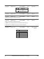
Contacts
The following list identifies important contacts within Honeywell.
Organization
Address
Technical Support
1-800-423-9883
Please have your instrument’s complete model number, serial number,
and software version available.
List of frequently asked questions and answers
1-888-423-9883
(Honeywell’s TACFACS: USA and
Canada only)
http://support.totalplant.honeywell.com
(Honeywell’s web site)
5/99
Honeywell Binary Serial Communications – User Manual
iii
Contents
1.
INTRODUCTION
1
2.
OVERVIEW
2
3.
NETWORK CONFIGURATION
3
3.1
Communication Levels
3.2 Physical Configuration
3.2.1
Terminations and Interconnections for RS-422/RS-485
4.
5.
UNIT CONFIGURATION
3
4
4
5
4.1
Unit Address
5
4.2
Parity and Baud Rate
5
DATA FORMATS
6
5.1 Binary Format
5.1.1
Number Conversions
5.1.1.1 BINARY TO DECIMAL CONVERSION
5.1.1.2 DECIMAL TO BINARY CONVERSION
5.1.2
8-Bit Binary Format
5.1.3
16-Bit Binary Format
5.1.4
32-Bit Binary Format
6
6
6
6
7
7
7
5.2 Text Format
5.2.1
ASCII CODE AND CHARACTER SET
7
8
5.3 Floating Point Format
5.3.1
IEEE 754 Format
5.3.1
Mantissa and Sign
5.3.2
Exponent
5.3.3
Mantissa and Exponent Combination
5.3.4
Reserved Operands
8
8
9
9
10
10
6
COMMUNICATION CONVENTIONS
11
7
DATA LINK LEVEL CONTROL
12
iv
7.1
Transparency Data Encoding
12
7.2
Control Encoding
12
7.3
Data Encoding
12
Honeywell Binary Serial Communications – User Manual
5/99
7.4 Data Transmission Control
7.4.1
Transmission Off
7.4.2
Transmission On
7.4.3
Abort
12
12
12
12
MESSAGE FORMAT
13
8
8.1
STX – Start of Text
13
8.2
UNIT –Unit Identification
13
8.3 MODE – Response Identification
8.3.1
Response Turnaround
8.3.2
Request Simple Poll
8.3.3
Data Block Continuation
8.3.4
Request Configuration Download
8.3.5
Response Mode
8.3.5.1 Read
8.3.5.2 Write
8.3.5.3 Simple Poll
8.3.5.4 Repoll
8.3.5.5 A-NAK
8.3.5.6 A-ACK
8.3.5.7 Pass Through
13
13
14
14
14
14
14
15
15
15
15
15
15
8.4
TYPE, ADDR – Data Identification and Transfer
15
8.5
DATA
16
8.6
ETX – End of Text
16
8.7
CHK – Checksum Error Detection
16
9
SAMPLE PROTOCOL EXCHANGES
17
9.1 Read
9.1.1
Read Single Request - No Error Detected
9.1.2
Read Multiple Request - No Error Detected
9.1.3
Read – Error Detected at the Data Link Level
9.1.4
Read – Error Detected at the Application Level
17
17
18
19
19
9.2 Write
9.2.1
Write – No Error Detected
9.2.2
Write – Error Detected at the Data Link Level
9.2.3
Write – Error Detected at the Application Level
20
20
21
21
9.3 Read With Repoll
9.3.1
Read With Repoll – No Error Detected
9.3.2
Read With Repoll – Error Detected at the Data Link Level
9.3.3
Read With Repoll – Error Detected at the Application Level
22
22
23
24
9.4 Write With Repoll
9.4.1
Write With Repoll – No Error Detected
24
24
5/99
Honeywell Binary Serial Communications – User Manual
v
9.4.2
9.4.3
9.5
Write With Repoll – Error Detected at the Data Link Level
Write With Repoll – Error Detected at the Application Level
Simple Poll
25
25
26
9.6 Data Continuation
9.6.1
Read
9.6.2
Write
10 COMMON MISTAKES DEVELOPING DRIVER SOFTWARE
26
27
28
29
10.1
Checksum Calculation
29
10.2
Forgotten A-ACK
29
10.3
IEEE Floating Point Format Problems
29
11. COMMUNICATION SUMMARY
30
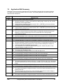
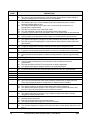
12. APPLICATION NAK SUMMARY
49
13. APPLICATION MESSAGES DETAIL
56
14. CTX/UDC5300/RSX/VPR/VRX CONFIGURATION PROTOCOL
97
14.1
Download Protocol
14.2
Upload Protocol
14.2.1 Control Message
14.2.2 Data Message
14.2.3 Example Upload Sequence For Entire Configuration
14.2.4 Clear Configuration:
14.3
Configuration Language Overview (LNC, LNL, LNS)
14.3.1 Grammar
14.3.2 Example LNC
vi
Honeywell Binary Serial Communications – User Manual
97
98
98
98
98
99
99
99
101
5/99
1.
Introduction
This manual covers use of the serial digital communications interface to the following Honeywell
instruments: Speedomax 25000 Recorder, Micromax LPU (Local Processing Unit), CTX/UDC5300, RSX,
VPR and VRX. The term “Unit” is used throughout this document as a general reference to these
instruments.
The serial digital communications interface is bi-directional: data can be read from as well as written to
each unit. All electrical design complies with EIA Standard RS-422A and EIA Standard RS-485. A
jumper-selectable RS232C interface is also available on the 25000 Recorder only. Protocol is modeled
after ANSI X3.28 “Procedures for the Use of the Communication Control Characters of American
National Standard Code for Information Interchange in Specified Data Links”.
5/99
Honeywell Binary Serial Communications – User Manual
1
2.
Overview
This serial digital communication interface is designed for a single Host computer with multiple Units. It is
a dedicated “Master-to-Slave” type, where the Unit is the “Slave” responding to the “Master”, or Host
computer, request. No direct Unit-to-Unit path can be established; each Unit listens only to the Host
computer.
MODES OF RESPONSE
The protocol provides a choice of two primary modes of response when data is requested from a Unit:
1. The Host computer can elect to wait for data to be sent back from the Unit immediately ( i.e., within
the expected response turn-around time).
2. The Host computer can elect to make a request for data from a Unit and then later repoll the unit for
the data.
A variation of the second response mode is when the Host computer requests data from all Units, and
then later repolls for the data. This mode of response is referred to as “Broadcast”.
SINGLE ACCESS REQUESTS
The most common Host computer request to a Unit is composed of a single access: read, write, or
repoll.
MULTIPLE ACCESS REQUESTS
This enhancement of the protocol allows for a single transaction to be composed of multiple access
requests (reads and/or writes). The following restrictions apply:
1. Receive Length - The received application message must not exceed 2000 bytes.
2. Transmit Length - The transmitted application message must not exceed 2000 bytes. If a Read
request detects buffer overflow, an error indication is returned.
3. The Repoll Host computer request remains a single transaction.
4. A Simple Poll Request can be issued starting with any mode byte of a multiple access request.
FIXED DATA PACKETS
The protocol provides for the read and write of specified “Packets” of data in order to minimize link
transaction time.
DYNAMICALLY ALLOCATED DATA PACKETS
The addition of this feature to the Micromax and Speedomax 25000 lines allows the Host computer to
dynamically describe the packets or blocks of data being requested. This approach reduces the number
of required fixed data packets.
2
Honeywell Binary Serial Communications – User Manual
5/99
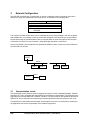
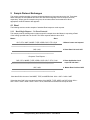
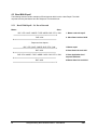
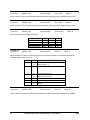
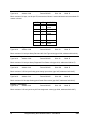
3.
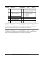
Network Configuration
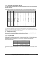
If the RS-485 multi-drop type of configuration is used, the maximum number of physical connections
(drops) on a single link is dependent on the type of Unit, as indicated in the following table:
UNIT CLASS
Speedomax 25000
Micromax 1
Micromax 2
CTX/UDC5300/RSX/
VPR/VRX
CONNECTIONS
60
30
60
31
The maximum number of links which can be used depends on the ports available in the Host computer.
With multiple links, it is possible to have up to 254 Units assigned, each identified by a unique address.
No data interchange is possible between Units, except that which is routed through the Host computer.
Transmission is over a four wire connection, using half-duplex operation in most cases.
A three wire RS232 is also provided for the Speedomax 25000 recorder, but the link is then restricted to
one Host and one recorder.
HOST
RS422
Unit 1
Unit 2
....
Unit n-1
Unit n
RS232
HOST
3.1
Unit
Communication Levels
The serial digital communications interface supports two layers or levels of hardware/software: Physical
and Data Link. This is consistent with the ISO/OSI Communications Layered Model. The Physical level is
supported by the RS-422A/RS-485 or RS232C interface. The Data Link level uses guidelines provided in
ANSI X3.28, and is responsible for maintaining an interchange between the Host computer and a unit.
The Network level, which determines the path, and the higher levels of the communications model up to
the Application level are the responsibility of the software programmer.
5/99
Honeywell Binary Serial Communications – User Manual
3
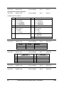
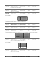
3.2
Physical Configuration
3.2.1
Terminations and Interconnections for RS-422/RS-485
The location at which the cables from the Host computer’s RS-422/RS-422 port terminate at a Unit is
found in the table below. Each screw terminal on the board accepts two #22 gage conductors. The
recommended cable type is two twisted pairs, each pair of which is shielded (typical Belden No. 8723 or
8728). The maximum recommended cable length is listed in the last column of the table.
A terminating resistor is provided on the receive port of every unit. It must be used only in the last unit on
the communication link. It is selected by positioning the unit’s associated jumper(s) as indicated in the
table.
For Host computers with RS-232-C ports, use shielded 3 conductor, 22 AWG cable. The maximum
recommended cable length is 50 feet.
UNIT
Speedomax
25000
Micromax 1 LPU
Micromax 2 LPU
CTX/UDC5300/
RSX/VPR/VRX
4
TERMINATION
LOCATION
30-Terminal Board
5-Terminal Board (TB5)
5-Terminal Board (TB5)
Terminal Board
JUMPER
ID
Port A:
W1, W2
W3(RS485)
W3(RS232)
Port B:
W4, W5
W6(RS485)
W6(RS232)
W2
W2
W2, W3
JUMPER
POSITION
CABLE LENGTH
(FEET)
1-2
1-2
2-3
2000
1-2
1-2
2-3
1-2
1-2
1-2
1000
2000
2000
Honeywell Binary Serial Communications – User Manual
5/99
4.
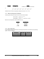
UNIT CONFIGURATION
Refer to the following manuals for detailed information concerning the configuration of a Unit:
UNIT
Speedomax
Micromax 2
CTX
UDC5300
RSX
VPR/VRX
4.1
PART
NUMBER
277800
70-MX-25-03
51-52-25-47
51-52-25-58
43-DR-25-10
57-77-25-15
MANUAL
25000 Recorder Operator’s Manual
Process Management System Instruction Manual
CTX Controller User Manual
UDC5300 User Manual
RSX Video Recorder User Manual
VPR/VRX Programmer Recorder User Manual
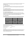
Unit Address
Each unit on the communications link requires a unique address, as indicated in the following table.
UNIT ADDRESS
(DECIMAL)
0
1-254
255
4.2
UNIT ADDRESS
(HEX)
00
01-FE
FF
DESCRIPTION
De-selects unit
Unit Address
De-selects unit
Parity and Baud Rate
The selection of odd, even, or no parity is dependent on the Host computer’s requirements; parity is
recommended.
The following table lists the baud rates available for selection for each type of Unit.
BAUD RATE
76800
38400
19200
9600
4800
2400
1200
5/99
BIT TIME
(MS)
0.01302
0.02604
0.05208
0.10417
0.20834
0.41668
0.83333
Speedomax 25000
Micromax LPU
X
X
X
X
X
X
X
Honeywell Binary Serial Communications – User Manual
CTX/UDC5300/RSX/
VPR/VRX
X
X
X
X
X
X
X
5
5.
Data Formats
The serial communications interface supports the following data formats: Binary, Text, and Floating
Point.
5.1
Binary Format
Binary format applies to data comprised of one or more contiguous unsigned bytes. In general, when
referring to bytes by number or position, the rightmost byte is the first byte (byte 1). Each byte consists of
8 bits. The data can be looked at as a stream of individual bits, or as individual bytes, depending on the
parameter.
5.1.1
Number Conversions
The follow section covers binary to decimal and decimal to binary conversions.
5.1.1.1 BINARY TO DECIMAL CONVERSION
The general equation for converting a binary (base 2) number to a decimal (base 10) number is the
following:
?10 = am 2 m + a m − 1 2 m − 1 +...+ a0 2 0 + a−1 2 −1 + ...+ a− ( n − 1) 2 − ( n − 1) + a− n 2 − n
Where:
?
a
m
= Decimal Number
= Coefficient (0 or 1)
= One less than the number of binary digits to the left of the
decimal point
= The number of binary digits to the right of the decimal point.
n
Example: Convert 110011.10101 to a decimal number.
Solution:
m=5
n=5
?10 = 1 × 2 5 + 1 × 2 4 + 0 × 2 3 + 0 × 2 2 + 1 × 2 1 + 1 × 2 0 + 1 × 2 −1 + 0 × 2 −2 + 1 × 2 −3 + 0 × 2 −4 + 1 × 2 −5
?10 = 32 + 16 + 0 + 0 + 2 + 1+ .5 + 0+ .125 + 0+ .03125
?10 = 51.66
5.1.1.2 DECIMAL TO BINARY CONVERSION
When converting an integer number from base 10 (decimal) to base 2 (binary), the integer to be
converted is repeatedly divided by 2. The consecutive divisions determine the coefficients (0 or 1) of
0
1
each binary digit. The first division corresponds to 2 , the second to 2 , and so on. If the number being
converted is divisible by 2, the power of two is multiplied by 0; while if a remainder is generated, the
power of two is multiplied by 1.
6
Honeywell Binary Serial Communications – User Manual
5/99
Example: Convert
2510 to its binary equivalent.
DIVISION
25 ÷ 2 = 12
12 ÷ 2 = 6
6÷2=3
3÷ 2 =1
1÷ 2 = 0
REMAINDER
1
0
0
1
1
POWER OF 2
20
21
22
23
24
Check:
2510 = 1 × 2 4 + 1 × 2 3 + 0 × 2 2 + 0 × 2 1 + 1 × 2 0
2510 = 16 + 8 + 0 + 0 + 1
5.1.2
8-Bit Binary Format
The 8-Bit Binary Format applies to data comprised of a single byte consisting of 8 bits, numbered from 7
to 0, left to right. Bit 7 is the high-order bit, and bit 0 is the low-order bit.
5.1.3
16-Bit Binary Format
The 16-Bit Binary Format applies to data comprised of two contiguous bytes. The bits are numbered from
15 to 0, left to right. Bit 15 is the high-order bit. Byte 1 contains bits 15 to 8; byte 2 contains bits 7 to 0.
5.1.4
32-Bit Binary Format
The 32-Bit Binary format applies to data comprised of four contiguous bytes. The bits are numbered from
31 to 0, left to right. Bit 31 is the high-order bit. Byte 4 contains bits 31-24, byte 3 contains bits 23 to 16,
and so on.
5.2
Text Format
Text format applies to data comprised of one or more contiguous bytes containing ASCII character
codes. In general, when referring to bytes by number or position, the leftmost byte is the first byte (byte
1). Each byte consists of 8 bits, numbered from 7 to 0. Bit 7 is the high-order bit, and bit 0 is the low-order
bit. Each bit number corresponds to an exponent of 2. Bits 6 to 0 contain the ASCII character code. For
example, the ASCII representation of the letter “A” in binary is 100 0001, which equals
1x2 6 + 0x2 5 + 0x2 4 + 0x2 3 + 0x2 2 + 0x2 1 + 1x2 0
or decimal 65 (hexadecimal 41).
5/99
Honeywell Binary Serial Communications – User Manual
7
5.2.1
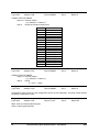
ASCII CODE AND CHARACTER SET
The codes detailed in the following table are per the ANSI Standard X3.4-1968 and are supported by all
Honeywell instruments.
Example: the letter (capital) A has a hexadecimal code of 41. Its binary representation is 0100 0001.
BITS
3-0
0000
0001
0010
0011
0100
0101
0110
0111
1000
1001
1010
1011
1100
1101
1110
1111
6-4
HEX
0
1
2
3
4
5
6
7
8
9
A
B
C
D
E
F
000
0
NUL
SOH
STX
ETX
EOT
ENQ
BEL
ACK
BS
HT
LF
VT
FF
CR
S0
S1
001
1
DLE
DC1
DC2
DC3
DC4
NAK
SYN
ETB
CAN
EM
SUB
ESC
FS
GS
RS
US
010
2
SP
!
“
#
$
%
&
‘
)
(
*
+
,
.
/
011
3
0
1
2
3
4
5
6
7
8
9
:
;
<
=
>
?
100
4
@
A
B
C
D
E
F
G
H
I
J
K
L
M
N
O
101
5
P
Q
R
S
T
U
V
W
X
Y
Z
¢
_
110
6
\
a
b
c
d
e
f
g
h
I
j
k
l
m
n
o
111
7
p
q
r
s
t
u
v
w
x
y
z
{
↑
}
°
DEL
The Speedomax 24000/25000 Series Recorder line also supports the use of hexadecimal codes 80
through AD of the IBM Extended ASCII character set. This portion of the extended character set includes
characters specific to the French and Spanish languages.
5.3 Floating Point Format
Floating point format is per the IEEE Standard for Binary Floating Point Arithmetic (TASK P754). This
format conforms to that of the Unit’s Math Firmware and/or Co-Processor.
5.3.1
IEEE 754 Format
The Floating Point data format consists of four contiguous bytes containing a 23-bit signed binary
mantissa with an 8-bit biased binary exponent. The bits are numbered from 31 to 0, left to right. Byte 4
contains bits 31-24, byte 3 contains bits 23 to 16, and so on. A description of the layout and
accompanying figure follow:
BITS
0-22
23-30
31
DESCRIPTION
Mantissa
Exponent: 8-bit unsigned value
Sign of the mantissa:
0 = positive, 1 = negative
An implied binary point exists between bits 22 and 23. Note that the transmission order is byte 1 to byte
4.
8
Honeywell Binary Serial Communications – User Manual
5/99
byte 4
byte 3
3
2 2
1
1
4 3
6
xxxxxxxx x.xxxxxxx
byte 2
1
5
8
xxxxxxxx
byte 1
7
0
xxxxxxx
mantissa (23 bits)
implied binary point
exponent
sign of the mantissa
The formula for calculating the floating point number is:
5.3.1
+ / −.mantissa x 2 exponent
Mantissa and Sign
The mantissa is defined by a sign bit (31) and a 23-bit binary fraction. This binary fraction is combined
with an “implied” value of 1 to create a mantissa value which is greater than or equal to 1.0 and less than
2.0.
The mantissa is positive if the sign bit is zero (reset), and negative if the sign bit is one (set). For
example:
DECIMAL
100
HEXADECIMAL
42C80000
BINARY
01000010 11001000 00000000 00000000
The sign bit is zero, indicating a positive mantissa. Removing the sign bits and exponent bits, the
mantissa becomes:
BINARY
xxxxxxxx x1001000 00000000 00000000
HEXADECIMAL
480000
Add an “implied” value of one to the left of the binary point:
BINARY
1.1001000 00000000 00000000
Using positioned notation, this binary number is equal to:
1.0 + (1x2 -1 ) + (0x2 -2 ) + (0x2 -3 ) + (1x2 -4 ) = 10
. + 0.5 + 0.0 + 0.0 + 0.0625 = 15625
.
5.3.2
Exponent
The exponent is defined by an unsigned 8-bit binary value (bits 23 through 30). The value of the
exponent is derived by performing a signed subtraction of 127 (decimal) from the 8-bit exponent value.
DECIMAL
100
HEXADECIMAL
42C80000
BINARY
01000010 11001000 00000000 00000000
removing the sign and mantissa bits, the exponent becomes:
5/99
Honeywell Binary Serial Communications – User Manual
9
DECIMAL
133
HEXADECIMAL
85
BINARY
x1000010 1xxxxxxx xxxxxxxx xxxxxxxx
or:
1x2 7 + 0x2 6 + 0x2 5 + 0x2 4 + 0x2 3 + 1x2 2 + 0x2 1 + 1x2 0
Subtract a bias of 127 from the exponent to determine its value: 133 – 127 = 6.
5.3.3
Mantissa and Exponent Combination
Combining the mantissa and exponent from the two previous examples:
float number = mantissa x 2 exponent
float number = 1.5625 x 2 6 = 15625
x 64 = 100.0
.
Below is a list of sample float values in IEEE 754 format:
DECIMAL
100.0
-100.0
0.5
-1.75
0.0625
5.3.4
HEXADECIMAL
42C80000
C2C80000
3F000000
BFE00000
3D800000
Reserved Operands
Per the Standard certain exceptional forms of floating point operands are excluded from the numbering
system. These are as follows:
EXCEPTION
+/- Infinity
Not-a-Number (NAN)
Denormalized Number
10
EXPONENT
All 1’s
All 1’s
All 0’s
MANTISSA
All 0’s
Other than 0’s
Other than 0’s
Honeywell Binary Serial Communications – User Manual
5/99
6
COMMUNICATION CONVENTIONS
The data transfer is half-duplex, using a 4-wire connection and a fifth wire used for a common. Data
transmission is asynchronous. The data format, detailed in Section 5, is a “Non-Return-to-Zero” (NRZ)
format; i.e., the bit level is maintained for the entire bit time. Additional bits of information are attached to
each byte delineating its Start, Stop, and Parity (if Parity applies to the Unit):
Start Bit (0) / Data (8 Bits) / Parity Bit / Stop Bit (1)
5/99
Honeywell Binary Serial Communications – User Manual
11
7
DATA LINK LEVEL CONTROL
7.1 Transparency Data Encoding
The protocol uses the Data Link Escape (DLE) method of encoding to differentiate communication
control characters from the binary data transmission. This method is consistent with ANSI X3.28.
7.2 Control Encoding
In order to be interpreted as a control character, the following codes must be immediately preceded by
the DLE (0x10) code:
FUNCTION
Abort
Acknowledge
End of Text
Not Acknowledge
Start of Text
Transmission Off
Transmission On
LABEL
ENQ
ACK
ETX
NAK
STX
DC2
DC1
CODE
0x05
0x06
0x03
0x15
0x02
0x12
0x11
7.3 Data Encoding
Whenever the DLE character is encountered in the data, it is sent twice to prevent the byte that follows
from being interpreted as a control character.
7.4 Data Transmission Control
The following control codes control the data flow from the Unit (Slave) to the Host computer (Master).
7.4.1
Transmission Off
When the Unit receives the Transmission Off/STOP (DLE DC2) control code, it stops its transmission to
the Host computer. The Unit resumes transmission upon receipt of a Transmission On/START control
code. Receiving an Abort (ENQ) or Start of Text (STX) aborts the transmission and previous request.
The Unit is then ready to respond to a new request.
Note that upon receipt of the Transmission Off/STOP request, a maximum of 10 characters will be
transmitted before the transmission actually stops.
7.4.2
Transmission On
Upon receipt of a Transmission On/START (DLE DC1) request, the Unit reactivates transmission.
7.4.3
Abort
Upon receipt of the Abort (DLE ENQ) request, the Unit terminates transmission and the previous request.
The Unit is then ready to respond to a new request.
12
Honeywell Binary Serial Communications – User Manual
5/99
8
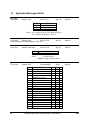
Message Format
The figures below lay out the general structure of a message from the Host computer (Master) to a Unit
(Slave), and from a Unit to the Host Computer.
Host Computer to Unit - READ
DLE
STX
UNIT
MODE
TYPE
ADDR
DLE
ETX
CHK
Unit to Host Computer - READ
DLE
STX
MODE
TYPE
ADDR
DA
…
TA
DLE
STX
CHK
Note that the UNIT field appears only in Master to Slave messages. The MODE field determines the
presence of the TYPE, ADDR, and DATA fields. If the message is a multiple access request, then more
than one MODE [, TYPE, ADDR, DATA] grouping is present, and the message may contain both reads
and writes.
8.1 STX – Start of Text
The STX field delineates the beginning of a message at the Data Link level. It consists of two bytes and
contains the DLE character followed by the Start of Text communications control code: DLE STX.
8.2 UNIT –Unit Identification
The UNIT field is used by the Host computer at the Data Link level to identify the target Unit. It consists of
one byte and contains a Unit’s unique address (refer to Section 4.1). If a Unit’s address is de-selected
(i.e., equals 0x00 or 0xFF), that Unit will not listen to the communications port.
Instead of a particular Unit’s address, the Host computer may send the “NO SELECT” (0x00) or
“BROADCAST” (0xFF) codes. In the No Select situation, no Unit responds to the Host computer’s
message. In the Broadcast situation, all Units listen to the Host computer’s message, but there is no
response from the Units, not even at the Data Link level.
8.3 MODE – Response Identification
The MODE field contains several pieces of information, as described below. It consists of a single byte,
with the bits numbered from left to right, 7 to 0.
BIT
7
6
5
4
0-3
8.3.1
DESCRIPTION
Response Turnaround
Request Simple Poll
Data Block Continuation
Request Configuration Download
Response Mode
SECTION
8.3.1
8.3.2
8.3.3
8.3.4
8.3.5
Response Turnaround
The Response Turnaround bit of the MODE field defines the type of response turnaround expected by
the Host computer.
If this bit is reset (0), the Host computer expects an immediate Data Link level acknowledge (ACK: 0x06)
with the Application Level data following in an accepted period of time.
5/99
Honeywell Binary Serial Communications – User Manual
13
If this bit is set (1), the Host computer expects only an immediate Data Link level acknowledge. The Host
computer will later repoll the Unit and at that time will there be an Application Level response
(acknowledge or data).
8.3.2
Request Simple Poll
The Request Simple Poll bit is used by the Unit to signal the Host computer that it has a status change
for an off-normal condition. By setting this bit, the Unit is requesting the Host computer to poll for this
data.
8.3.3
Data Block Continuation
The Data Field Continuation bit is used by the Micromax LPU to indicate to the Host computer that the
amount of data to be transmitted exceeds the allowable message length. By setting this bit, the Unit
indicates to the Host computer that the present data block is full and that more data will be transmitted
when the Host issues a new request.
8.3.4
Request Configuration Download
The Request Configuration Download bit is used by the Micromax LPU to signal the Host computer
(Master Station) that a configuration download is necessary. By setting this bit, the Unit is requesting the
Host computer to return configuration information via the Pass Through response mode. In turn, the Unit
will pass the configuration data on to its Local Station Host computer’s Application level.
8.3.5
Response Mode
The Response Mode sub-field consists of 4 bits and contains a code representing the Host computer’s
desired response from the Unit, and the Unit’s response in return, as described in the following table.
HOST TO UNIT:
Read
Write
Simple Poll
Repoll
CODE
0x01
0x02
0x07
0x08
SECTION
8.3.5.1
8.3.5.2
8.3.5.3
8.3.5.4
UNIT TO HOST:
Application Level A-NAK
Application Level A-ACK
Pass Through
CODE
0x09
0x0A
0x0B
SECTION
8.3.5.5
8.3.5.6
8.3.5.7
The response turnaround time for the Repoll response mode is typically within a few character times.
That for the Read/Write response modes, from the Host computer request to start of DATA or A-ACK
from the Unit’s Application level, is as follows:
Single/Group Read (Flt. Pt.)
Single Write (Flt. Pt.)
500 milliseconds
1 second
8.3.5.1 Read
The Host computer issues a Read (0x01) request when it desires to access data from a Unit. This type of
request requires the presence of the TYPE and ADDR fields (Section 8.4) which identify the data for
transfer. If the Response Turnaround bit is set, the Host computer does not expect any response from
the Unit, as it will later Repoll for the data.
14
Honeywell Binary Serial Communications – User Manual
5/99
If the Read request is successful, the Unit responds with a message containing the MODE, TYPE, ADDR
and associated data in the DATA field (Section 8.5). Otherwise, the Unit returns an A-NAK followed by
the corresponding reason code for the error.
8.3.5.2 Write
The Host computer issues a Write (0x02) request when it has data to be written to a Unit. This type of
request requires the presence of the TYPE, ADDR, and DATA fields which identify the data for transfer. If
the Response Turnaround bit is set, the Host computer does not expect any response from the Unit, as it
will later Repoll for the status of the Write request.
If the Write request is successful, the Unit responds with an A-ACK. Otherwise, the Unit returns an ANAK followed by the corresponding reason code for the error.
8.3.5.3 Simple Poll
The Host computer issues a Simple Poll (0x07) request upon receipt of a response which has the
Request Simple Poll bit set. A Unit can set this bit on the detection of an alarm, event, or diagnostic
change. This type of request requires only the presence of the MODE field. In response to this request
from the Host computer, the Unit responds with a TYPE 0x19, ADDR 0x03 data packet and clears the
request bit.
The Host computer can also issue this request at frequent intervals for alarm or diagnostic polling. If a
Unit does not have any information for the Host computer, it returns an A-NAK with reason code 007.
8.3.5.4 Repoll
The Host computer issues a Repoll (0x08) request when a previous Read or Write request had been
issued with the Response Turnaround bit set. If that previous request had not been successful, the Unit
returns an A-NAK with the corresponding reason code.
For a successful Write, the Unit responds with an A-ACK. For a successful Read, the Unit responds with
the requested data in the DATA field.
8.3.5.5 A-NAK
The A-NAK (0x09) response mode indicates that a Unit could not acknowledge (i.e., successfully
complete) the Host computer’s request. This response mode requires only the presence of the DATA
field which consists of a single byte and contains a code representing the reason for the failure. Section
0, Application NAK Summary, contains a complete list of all reason codes and associated descriptions.
8.3.5.6 A-ACK
The Unit responds with an A-ACK (0x0A) response mode to indicate the successful completion of a Host
computer Write request. This response also occurs after a Repoll for a previous Write request. No other
information is required with this response.
8.3.5.7 Pass Through
The Pass Through (0x0B) response mode applies only to the Micromax LPU. The Master Station Host
computer issues a Pass Through request upon receipt of a response which has the Request
Configuration Download bit set. This response mode informs the Unit that the following message is to be
passed on to its Local Station Host computer’s Application level.
8.4 TYPE, ADDR – Data Identification and Transfer
The TYPE and ADDR fields uniquely identify the data for transfer. TYPE is a one byte field. It contains a
number (0x00 – 0xFF) which represents a general parameter category selection. TYPEs fall into the
following broad classifications:
5/99
Honeywell Binary Serial Communications – User Manual
15
1.
2.
3.
4.
5.
Single – a single parameter or item reference
Program/Packet – a collection of Single items
Recipe – a binary block of data
Dynamic Packet – a special case of item 2 where the Host computer defines the list of Single items
Dynamic Block – a special case of item 3 where the Host computer can define the starting address
and size of a binary memory dump
ADDR is a one byte field which is a further breakdown of the TYPE classification. It contains a number
(0x00 – 0xFF) which is a specific index to an item within the general parameter category.
For example, TYPE 0x03 ADDR 0x01 refers to Loop 1’s Process Variable. Section 0, 5.3 Floating Point
Format.
Communication Summary, contains descriptions of all data available for transfer.
8.5 DATA
The DATA field is present in the following situations:
1. When the Host computer sends a Write request to a Unit
2. When the Unit responds with the data from a successful Read request
3. When the Unit responds after the detection of an error at the Application Level
The size and contents of this field are dependent on the parameter (TYPE, ADDR) being successfully
read/written in situations 1 and 2 above. Section 0, 5.3 Floating Point Format.
Communication Summary, contains descriptions of all data available for transfer.
When an error is detected at the Application level, this field consists of a single byte containing a code
representing the reason for the error. Section 0, 5.3 Floating Point Format.
Communication Summary, lists all codes and associated error conditions.
8.6 ETX – End of Text
The ETX field delineates the end of a message at the Data Link level. It consists of two bytes and
contains the DLE character followed by the End of Text communications control code: DLE ETX.
8.7 CHK – Checksum Error Detection
The CHK (checksum) field is used at the Data Link level to provide error detection of data blocks. (This is
in addition to the parity which is generated on each byte.) It consists of a single byte.
The associated algorithm adds the bytes comprising the MODE, TYPE, ADDR, and DATA fields; the
UNIT field is NOT included. The sum (truncated if necessary to 8 bits) follows the ETX field. Note that the
summation does not include duplicate DLE (i.e., data transparency) characters encountered in those
fields. Also note that when this byte is transmitted, data transparency is applied to it; that is, if it equals
the value of the DLE character, it will be transmitted twice.
16
Honeywell Binary Serial Communications – User Manual
5/99
9
Sample Protocol Exchanges
This section contains samples of protocol exchanges between a Host computer and a Unit. Throughout
these examples, the terms Master and Slave are used interchangeably for Host computer and Unit,
respectively. Where specific examples are given, the numbers shown are hexadecimal. Where
appropriate, the DLE character also appears.
9.1 Read
The following sections contain samples of standard Read response mode requests.
9.1.1
Read Single Request - No Error Detected
This sample protocol exchange also includes a specific example where the Master is requesting a Read
of the Analog Input #06 value for Unit 05. The Slave responds with the value 100.0.
Master
Slave
DLE / STX / UNIT / MODE / TYPE / ADDR / DLE / ETX / CHK
0x10 / 0x02 / 0x05 / 0x01 / 0x07 / 0x06 / 0x10 / 0x03 / 0x0E
-------------------------------------------------------------------------------------È
1. Master issues read request *
DLE / ACK
0x10 / 0x06
Ç------------------------------------------------------------------------------------
2. Slave Data Link level ACK
. . . Response Time Elapses . . .
DLE / STX / MODE / TYPE / ADDR / DATA / DLE / ETX / CHK
0x10 / 0x02 / 0x01 / 0x07 / 0x06 / 0x00 00 C8 42 / 0x10 / 0x03 / 0x18
Ç-----------------------------------------------------------------------------------DLE / ACK
0x10 / 0x06
-------------------------------------------------------------------------------------È
3. Slave Application Level
responds with data **
4. Master Data Link level ACK
*Note that CHK is the sum of the MODE, TYPE, and ADDR fields: 0x01 + 0x07 + 0x06 = 0x0E.
**Note that here CHK is the truncated summation of the MODE, TYPE, ADDR, and DATA fields: 0x01 +
0x07 + 0x06 + 0x00 + 0x00 +0xC8 + 0x42 = 0x118, which when truncated to 8 bits equals 0x18.
5/99
Honeywell Binary Serial Communications – User Manual
17
9.1.2
Read Multiple Request - No Error Detected
This sample protocol exchange also includes a specific example where the Master is requesting a Read
of the Analog Input #06 and Analog Input #2 values for Unit 05. The Slave responds with the value 100.0.
Master
Slave
DLE / STX / UNIT / MODE / TYPE / ADDR / MODE / TYPE / ADDR / DLE / ETX /
CHK
0x10 / 0x02 / 0x05 / 0x01 / 0x07 / 0x06 / 0x01 / 0x07 / 0x02 / 0x10 / 0x03 / 0x18
-------------------------------------------------------------------------------------È
1. Master issues read
DLE / ACK
0x10 / 0x06
Ç------------------------------------------------------------------------------------
2. Slave Data Link
level ACK
request *
. . . Response Time Elapses . . .
DLE / STX / MODE / TYPE / ADDR / DATA / DLE / ETX / CHK
0x10 / 0x02 / 0x01 / 0x07 / 0x06 / 0x00 00 C8 42 / 0x01 / 0x07 / 0x06 / 0x00 00 C8 42
/ 0x10 / 0x03 / 0x2C
Ç-----------------------------------------------------------------------------------DLE / ACK
0x10 / 0x06
-------------------------------------------------------------------------------------È
3. Slave Application
Level responds
with data **
4. Master Data Link level ACK
*Note that CHK is the sum of all the MODE, TYPE, and ADDR fields:
0x01 + 0x07 + 0x06 + 0x01 + 0x07 + 0x02 = 0x018
**Note that here CHK is the truncated summation of the MODE, TYPE, ADDR, and DATA fields:
0x01 + 0x07 + 0x06 + 0x00 + 0x00 +0xC8 + 0x42 + 0x01 + 0x07 + 0x02 + 0x00 + 0x00 +0xC8 + 0x42 =
0x22C, which when truncated to 8 bits equals 0x2C.
18
Honeywell Binary Serial Communications – User Manual
5/99
9.1.3
Read – Error Detected at the Data Link Level
This sample protocol exchange outlines a transaction where an error is detected at the Data Link level:
Master
Slave
DLE / STX / UNIT / MODE / TYPE / ADDR / DLE / ETX /CHK
------------------------------------------------------------------------------È
DLE / NAK
Ç----------------------------------------------------------------------------DLE / STX / UNIT / MODE / TYPE / ADDR / DLE/ ETX / CHK
------------------------------------------------------------------------------È
DLE / ACK
Ç----------------------------------------------------------------------------.
1. Master issues read request
2. Slave Data Link level NAK
3. Master re-transmits request
4. Slave Data Link level ACK
. . Response time elapses . . .
DLE / STX / MODE / TYPE / ADDR / DATA / DLE / ETX / CHK
Ç----------------------------------------------------------------------------DLE / NAK
------------------------------------------------------------------------------È
DLE / STX / MODE / TYPE / ADDR / DATA / DLE / ETX / CHK
Ç----------------------------------------------------------------------------DLE / ACK
------------------------------------------------------------------------------È
9.1.4
5. Slave Application Level
responds with data
6. Master Data Link level NAK
7. Slave re-transmits data
8. Master Data Link level ACK
Read – Error Detected at the Application Level
This sample protocol exchange outlines a transaction where an error is detected at the Application level.
In this situation, the Slave responds with A-NAK and associated reason code for data. The Master
acknowledges and will act accordingly.
Master
Slave
DLE / STX / UNIT / MODE / TYPE / ADDR / DLE / ETX / CHK
------------------------------------------------------------------------------È
DLE / ACK
Ç-----------------------------------------------------------------------------
1. Master issues read request
2. Slave Data Link level ACK
. . . Response Time Elapses . . .
DLE / STX / A-NAK / DATA / DLE / ETX / CHK
Ç----------------------------------------------------------------------------DLE / ACK
------------------------------------------------------------------------------È
5/99
Honeywell Binary Serial Communications – User Manual
3. Slave Application level
responds with A-NAK
4. Master Data Link level ACK
19
9.2 Write
The following sections contain samples of standard Write response mode requests.
9.2.1
Write – No Error Detected
This sample protocol exchange also includes a specific example where the Master is requesting a Write
of the value 100.0 to the Constant Value #3 of Unit 0x01.
Master
Slave
DLE / STX / UNIT / MODE / TYPE / ADDR / DATA / DLE / ETX / CHK
0x10 / 0x02 / 0x01 / 0x02 / 0x25 / 0x03 / 0x0000C842 / 0x10 / 0x03 / 0x34
-------------------------------------------------------------------------- -------------È
DLE / ACK
0x10 / 0x06
Ç----------------------------------------------------------------------------------------
1. Master issues write
request *
2. Slave Data Link level ACK
. . . Response time elapses . . .
DLE / STX / A-ACK / DLE / ETX / CHK
0x10 / 0x02 / 0x0A / 0x10 / 0x03 / 0x0A
Ç---------------------------------------------------------------------------------------DLE / ACK
0x10 / 0x06
----------------------------------------------------------------------------------------È
3. Slave Application Level
A-ACK
4. Master Data Link level ACK
*Note that here CHK is the truncated summation of the MODE, TYPE, ADDR, and DATA fields: 0x02 +
0x25 + 0x03 + 0x00 + 0x00 +0xC8 + 0x42 = 0x134, which when truncated to 8 bits equals 0x34.
**Note that since only the MODE field is present, CHK equals A-ACK, 0x0A.
20
Honeywell Binary Serial Communications – User Manual
5/99
9.2.2
Write – Error Detected at the Data Link Level
This sample protocol exchange outlines a transaction where an error is detected at the Data Link level:
Master
Slave
DLE / STX / UNIT / MODE / TYPE / ADDR / DATA / DLE / ETX / CHK
-------------------------------------------------------------------------------È
DLE / NAK
Ç-----------------------------------------------------------------------------DLE / STX / UNIT / MODE / TYPE / ADDR / DATA / DLE / ETX / CHK
-------------------------------------------------------------------------------È
DLE / ACK
Ç------------------------------------------------------------------------------
1. Master issues write request
2. Slave Data Link level NAK
3. Master retransmits
4. Slave Data Link level ACK
. . . Response time elapses . . .
DLE / STX / A-ACK / DLE / ETX / CHK
Ç------------------------------------------------------------------------------DLE / ACK
-------------------------------------------------------------------------------È
9.2.3
5. Slave Application level A-ACK
6. Master Data Link level ACK
Write – Error Detected at the Application Level
This sample protocol exchange outlines a transaction where an error is detected at the Application level.
In this situation, the Slave responds with A-NAK and associated reason code for data; the current request
is ignored. The Master acknowledges and will act accordingly.
Master
Slave
DLE / STX / UNIT / MODE / TYPE / ADDR / DATA / DLE / ETX / CHK
------------------------------------------------------------------------------È
DLE / ACK
Ç-----------------------------------------------------------------------------
1. Master issues write request
2. Slave Data Link level ACK
. . . Response time elapses . . .
DLE / STX / A-NAK / DATA / DLE / ETX / CHK
Ç----------------------------------------------------------------------------DLE / ACK
-------------------------------------------------------------------------------È
5/99
Honeywell Binary Serial Communications – User Manual
3. Slave Application level A-NAK
4. Master Data Link level ACK
21
9.3 Read With Repoll
The following sections contain examples of Read requests which involve a later Repoll. The initial
requests issued by the Master have the Response Turnaround bit set.
9.3.1
Read With Repoll – No Error Detected
Master
Slave
DLE / STX / UNIT / MODE / TYPE / ADDR / DLE / ETX / CHK
-------------------------------------------------------------------------------È
DLE / ACK
Ç-------------------------------------------------------------------------------
1. Master read with repoll
2. Slave Data Link level ACK
. . . Response time elapses . . .
DLE / STX / UNIT / MODE / DLE / ETX / CHK
-------------------------------------------------------------------------------È
DLE / ACK
Ç-----------------------------------------------------------------------------DLE / STX / MODE / TYPE / ADDR / DATA / DLE / ETX / CHK
Ç-----------------------------------------------------------------------------DLE / ACK
-------------------------------------------------------------------------------È
22
Honeywell Binary Serial Communications – User Manual
1. Master repoll
2. Slave Data Link level ACK
3. Slave Application level
responds with data
4. Master Data Link level ACK
5/99
9.3.2
Read With Repoll – Error Detected at the Data Link Level
This sample protocol exchange outlines a transaction where an error is detected at the Data Link level:
Master
Slave
DLE / STX / UNIT / MODE / TYPE / ADDR / DLE / ETX / CHK
-------------------------------------------------------------------------------È
DLE / NAK
Ç------------------------------------------------------------------------------DLE / STX / UNIT / MODE / TYPE / ADDR / DLE / ETX / CHK
-------------------------------------------------------------------------------È
DLE / ACK
Ç-------------------------------------------------------------------------------
1. Master read with repoll
2. Slave Data Link level NAK
3. Master re-transmits
4. Slave Data Link level ACK
. . . Response time elapses . . .
DLE / STX / UNIT / MODE / DLE / ETX / CHK
-------------------------------------------------------------------------------È
DLE / NAK
Ç------------------------------------------------------------------------------DLE / STX / UNIT / MODE / DLE / ETX / CHK
-------------------------------------------------------------------------------È
DLE / ACK
Ç------------------------------------------------------------------------------DLE / STX / MODE / TYPE / ADDR / DATA / DLE / ETX / CHK
Ç------------------------------------------------------------------------------DLE / ACK
-------------------------------------------------------------------------------È
5/99
Honeywell Binary Serial Communications – User Manual
1. Master repoll
2. Slave Data Link level NAK
3. Master re-transmits
4. Slave Data Link level ACK
5. Slave Application level
responds with data
6. Master Data Link level ACK
23
9.3.3
Read With Repoll – Error Detected at the Application Level
This sample protocol exchange outlines a transaction where an error is detected at the Application level.
In this situation, the Slave responds with A-NAK and associated reason code for data; the current request
is ignored. The Master acknowledges and will act accordingly.
Master
Slave
DLE / STX / UNIT / MODE / TYPE / ADDR / DLE / ETX / CHK
--------------------------------------------------------------------------È
DLE / ACK
Ç--------------------------------------------------------------------------
1. Master read with repoll
2. Slave Data Link level ACK
. . Response time elapses . . .
DLE / STX / UNIT / MODE / DLE / ETX / CHK
--------------------------------------------------------------------------È
DLE / ACK
Ç-------------------------------------------------------------------------DLE / STX / A-NAK / DATA / DLE / ETX / CHK
Ç-------------------------------------------------------------------------DLE / ACK
--------------------------------------------------------------------------È
3. Master repoll
4. Slave Data Link level ACK
5. Slave Application level A-NAK
6. Master Data Link level ACK
9.4 Write With Repoll
The following sections contain examples of Write requests which involve a later Repoll. The initial
requests issued by the Master have the Response Turnaround bit set.
9.4.1
Write With Repoll – No Error Detected
Master
Slave
DLE / STX / UNIT / MODE / TYPE / ADDR / DATA / DLE / ETX / CHK
-------------------------------------------------------------------------------È
DLE / ACK
Ç--------------------------------------------------------------------------------
1. Master write with repoll
2. Slave Data Link level ACK
. . . Response time elapses . . .
DLE / STX / UNIT / MODE / DLE / ETX / CHK
-------------------------------------------------------------------------------È
DLE / ACK
Ç-------------------------------------------------------------------------------DLE / STX / A-ACK / DLE / ETX / CHK
Ç-------------------------------------------------------------------------------DLE / ACK
-------------------------------------------------------------------------------È
24
Honeywell Binary Serial Communications – User Manual
3. Master repoll
4. Slave Data Link level ACK
5. Slave Application level A-ACK
6. Master Data Link level ACK
5/99
9.4.2
Write With Repoll – Error Detected at the Data Link Level
This sample protocol exchange outlines a transaction where an error is detected at the Data Link level:
Master
Slave
DLE / STX / UNIT / MODE / TYPE / ADDR / DATA / DLE / ETX / CHK
-------------------------------------------------------------------------------È
DLE / NAK
Ç------------------------------------------------------------------------------DLE / STX / UNIT / MODE / TYPE / ADDR / DATA / DLE / ETX / CHK
-------------------------------------------------------------------------------È
DLE / ACK
Ç-------------------------------------------------------------------------------
1. Master write with repoll
2. Slave Data Link level NAK
3. Master re-transmits
4. Slave Data Link level ACK
. . . Response time elapses . . .
DLE / STX / UNIT / MODE / DLE / ETX / CHK
-----------------------------------------------------------------------------È
DLE / ACK
Ç----------------------------------------------------------------------------DLE / STX / A-ACK / DLE / ETX / CHK
Ç----------------------------------------------------------------------------DLE / NAK
-----------------------------------------------------------------------------È
5. Master repoll
6. Slave Data Link level ACK
7. Slave Application level A-ACK
8. Master Data Link level NAK
DLE / STX / A-ACK / DLE / ETX / CHK
Ç----------------------------------------------------------------------------DLE / ACK
-----------------------------------------------------------------------------È
9.4.3
9. Slave re-transmits
10. Master Data Link level ACK
Write With Repoll – Error Detected at the Application Level
This sample protocol exchange outlines a transaction where an error is detected at the Application level.
In this situation, the Slave responds with A-NAK and associated reason code for data; the current request
is ignored. The Master acknowledges and will act accordingly.
Master
Slave
DLE / STX / UNIT / MODE / TYPE / ADDR / DATA / DLE / ETX / CHK
-----------------------------------------------------------------------------È
DLE / ACK
Ç----------------------------------------------------------------------------
1. Master write with repoll
2. Slave Data Link level ACK
. . . Response time elapses . . .
DLE / STX / UNIT / MODE / DLE / ETX / CHK
-----------------------------------------------------------------------------È
DLE / ACK
Ç----------------------------------------------------------------------------DLE / STX / A-NAK / DATA / DLE / ETX / CHK
Ç----------------------------------------------------------------------------DLE / ACK
-----------------------------------------------------------------------------È
5/99
3. Master repoll
4. Slave Data Link level ACK
5. Slave Application level A-NAK
6. Master Data Link level ACK
Honeywell Binary Serial Communications – User Manual
25
9.5 Simple Poll
The following sample illustrates a Simple Poll request. The first exchange is a standard read request
from the Master. The Application level response from the Slave has the Request Simple Poll (Section
8.3.2) bit set. This indication is recognized by the Master, who in turn issues a Simple Poll request.
Master
Slave
DLE / STX / UNIT / MODE / TYPE / ADDR / DLE / ETX / CHK
-----------------------------------------------------------------------------------È
DLE / ACK
Ç-----------------------------------------------------------------------------------
1. Master read request
2. Slave Data Link level ACK
. . . Response time elapses . . .
DLE / STX / MODE / TYPE / ADDR / DATA / DLE / ETX / CHK
Ç----------------------------------------------------------------------------------DLE / ACK
-----------------------------------------------------------------------------------È
...
DLE / STX / UNIT / MODE / DLE / ETX / CHK
-----------------------------------------------------------------------------------È
DLE / ACK
Ç-----------------------------------------------------------------------------------
3. Slave Application level
response: simple poll bit set
4. Master Data Link level ACK
5. Master simple poll request
6. Slave Data Link level ACK
. . . Response time elapses . . .
DLE / STX / MODE / TYPE / ADDR / DATA / DLE / ETX / CHK
Ç----------------------------------------------------------------------------------DLE / ACK
-----------------------------------------------------------------------------------È
7. Slave Application level
response: Type 0x19 Addr 0x03
8. Master Data Link level ACK
9.6 Data Continuation
The Micromax LPU provides for the transmission of large blocks of data in sections indicated by the Data
Block Continuation bit in the MODE field. The following sections contain sample protocol exchanges for
the Read and Write of large blocks of data.
26
Honeywell Binary Serial Communications – User Manual
5/99
9.6.1
Read
This following is the sample protocol when the Master reads a large block of data:
Master
Slave
DLE / STX / UNIT / MODE / TYPE / ADDR / DLE / ETX / CHK
------------------------------------------------------------------------------È
DLE / ACK
Ç------------------------------------------------------------------------------
1. Master read request
2. Slave Data Link level ACK
. . . Response time elapses . . .
DLE / STX / MODE / TYPE / ADDR / DATA / DLE / ETX / CHK
Ç------------------------------------------------------------------------------DLE / ACK
-------------------------------------------------------------------------------È
DLE / STX / UNIT / MODE / TYPE / ADDR / DLE / ETX / CHK /
-------------------------------------------------------------------------------È
DLE / ACK
Ç-------------------------------------------------------------------------------
3. Slave Application level
response: DBC bit set
4. Master Data Link level ACK
5. Master requests more data
6. Slave Data Link level ACK
. . . Response time elapses . . .
DLE / STX / MODE / TYPE / ADDR / DATA / DLE / ETX / CHK
Ç------------------------------------------------------------------------------DLE / ACK
-------------------------------------------------------------------------------È
5/99
Honeywell Binary Serial Communications – User Manual
7. Slave Application level
responds with data
8. Master Data Link level ACK
27
9.6.2
Write
This following is the sample protocol when the Master writes a large block of data:
Master
Slave
DLE / STX / UNIT / MODE / TYPE / ADDR / DATA / DLE / ETX / CHK
-------------------------------------------------------------------------------È
DLE / ACK
Ç-------------------------------------------------------------------------------
1. Master write request with
DBC bit set
2. Slave Data Link level ACK
. . . Response time elapses . . .
DLE / STX / A-ACK / DLE / ETX / CHK
Ç------------------------------------------------------------------------------DLE / ACK
DLE / STX / UNIT / MODE / TYPE / ADDR / DATA / DLE / ETX / CHK
-------------------------------------------------------------------------------È
DLE / ACK
Ç------------------------------------------------------------------------------
3. Slave Application level A-ACK
4. Master Data Link level ACK
5. Master write of more data
6. Slave Data Link level ACK
. . . Response time elapses . . .
DLE / STX / A-ACK / DLE / ETX / CHK
Ç------------------------------------------------------------------------------DLE / ACK
-------------------------------------------------------------------------------È
28
Honeywell Binary Serial Communications – User Manual
7. Slave Application level A-ACK
8. Master Data Link level ACK
5/99
10 Common Mistakes Developing Driver Software
The following sections address the most common problems when developing a software device driver for
these instruments, I hope this section helps avoid unnecessary development time.
10.1 Checksum Calculation
See Section 8.7, CHK – Checksum Error Detection
10.2 Forgotten A-ACK
See Section 9, Sample Protocol Exchanges
10.3 IEEE Floating Point Format Problems
See Section 5.3 Floating Point Format.
5/99
Honeywell Binary Serial Communications – User Manual
29
11.
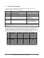
Communication Summary
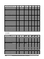
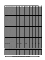
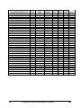
This section summarizes the Application Level data available for Read and/or Write access. The
information is presented in tabular format and includes:
HEADING
Parameter
Description
Type
Addr
Data Format
R/W
CONTENTS
Brief description of parameter available for
read and/or write access
General classification of parameter
Further breakdown of classification
BINARY/FLOAT/TEXT/BLOCK
Read/Write access
Size
Unit Code
Size of parameter
Type of Unit to which parameter applies
FOR MORE INFO
Section 8.4
Section 8.4
R: Read Only
W: Write Only
R/W: Read or Write
Number of bytes
S: Speedomax 25000
M: Micromax LPU (M1, M2)*
P: CTX/UDC5300/RSX/VPR/VRX
Family
Page
Reference to detailed description of parameter
*Where a distinction is needed between Micromax1 and Micromax2 M1 and M2 will be used as the unit
code. M1 represents all LPU(s) with software revisions A – G. M2 represents all LPU(s) with software
revisions >= H.
If a parameter is associated with a function block, a mnemonic for the function block appears as part of
the parameter description. A function block can apply to than one type of Unit. In these cases, the
address column may show a range: e.g., 0x01-xx. Refer to the following table to determine a parameter’s
end range value for the Speedomax and Micromax Units. NA indicates “Not Applicable”.
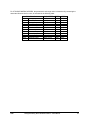
FUNCTION BLOCK
AI:
Analog Input
AL:
Alarm
AO:
Analog Output
CN:
Constant
CR:
Control Relays
CV:
Calculated Value
DI:
Discrete Input
DO:
Discrete Output
LP:
Control Loop
PP:
Pseudo Point
SPP: Setpoint Profiler
TL:
Totalizer
30
Speedomax
135
120
16
50
NA
NA
135
135
NA
60
NA
NA
Micromax1
75
150
16
100
999
NA
225
225
16
255
2
NA
Honeywell Binary Serial Communications – User Manual
Micromax2
225
150
16
200
999
NA
225
225
16
255
4
NA
5/99
For CTX/UDC5300/RSX/VPR/VRX, the parameter’s end range value is determined by accessing the
associated function block’s count, as indicated in the following table:
FUNCTION BLOCK
AI:
Analog Input
AL:
Alarm
AO:
Analog Output
CN:
Constant
CR:
Control Relay
CV:
Calculated Variable
DI:
Discrete Input
DO:
Discrete Output
LP:
Control Loop
PP:
Pseudo Point
SPP:
Setpoint Profile
TL:
Totalizer
5/99
PARAMETER
AI: Count
AL: Count
AO: Count
CN: Count
NA
CV: Count
DI: Count
DO: Count
LP: Count
NA
SPP: Count
TL: Count
TYPE
0x02
0x02
0x02
0x02
NA
0x02
0x02
0x02
0x02
NA
0x02
0x02
Honeywell Binary Serial Communications – User Manual
ADDR
0x51
0x56
0x52
0x55
NA
0x59
0x53
0x54
0x58
NA
0x57
0x60
31
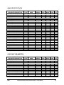
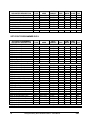
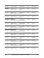
ANALOG INPUT DATA
ANALOG INPUT
PARAMETER DESCRIPTION
OUTPUTS:
AI: Output Value
AI: Output Values and Status
AI: RJ Compensation
PARAMETERS:
AI: Adjustment Value
AI: Count
AI: Default Value
AI: Engineering Units Text
AI: Engineering Units Text
AI: Function Block Description
AI: Function Block Description
AI: Function Block Tag
AI: Packet 1 – AI Output
AI: Packet 1 – AI Output
AI: Packet 6 – AI Status
AI: Packet 6 – AI Status
AI: Range High
AI: Range Low
AI: Raw Value
STATUS:
AI: Point Status/Assignment
TYPE
ADDR
DATA
FORMAT
SIZE
R/W
MODE
UNIT
CODE
PG.
0x07
0x9C
0x9B
0x01-xx
0x01-xx
0x01-xx
FLOAT
float+byte
FLOAT
4
5
4
R
R
R
S,M,P
S,M,P
S,M,P
68
89
89
0x15
0x02
0x95
0xCC
0xCC
0xC0
0xD6
0xC6
0x19
0x19
0x19
0x19
0xBB
0xBA
0x1A
0x01-xx
0x51
0x01-xx
0x01-0x87
0x01-xx
0x01-xx
0x01-xx
0x01-xx
0x00
0x12
0x05
0x16
0x01-xx
0x01-xx
0x01-xx
FLOAT
BINARY
FLOAT
TEXT
TEXT
TEXT
TEXT
TEXT
BLOCK
BLOCK
BLOCK
BLOCK
FLOAT
FLOAT
FLOAT
4
2
4
6
6
14
16
7
300
540
75
135
4
4
4
RW
R
R
RW
R
RW
RW
RW
R
R
R
R
R
R
R
S,M,P
P
S,M
S
P
S,P
P
S,P
M
S
M
S
S,M,P
S,M,P
P
71
66
89
93
93
92
94
93
71
74
72
74
92
92
75
0x28
0x01-xx
BINARY
1
R
S,M,P
77
R/W
MODE
UNIT
CODE
PG.
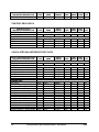
ALARM DATA
ALARM
PARAMETER DESCRIPTION
INPUTS:
AL: Set Point
OUTPUTS:
AL: Output Status
PARAMETERS:
AL: Count
AL: Function Block Description
AL: Function Block Tag
AL: Hysteresis
AL: Hysteresis
AL: Off Label Text
AL: On Label Text
AL: On/Off Label Text
AL: Packet 5 – AL Status Packed
32
TYPE
ADDR
DATA
FORMAT
SIZE
0x11
0x01-xx
FLOAT
4
RW
S,M,P
69
0x12
0x01-xx
BINARY
1
R
S,M,P
69
0x02
0xE1
0xE2
0x13
0x13
0xE4
0xE3
0xE5
0x19
0x56
0x01-xx
0x01-xx
0x00
0x01-xx
0x01-xx
0x01-xx
0x01-xx
0x04
BINARY
TEXT
TEXT
FLOAT
FLOAT
TEXT
TEXT
TEXT
BLOCK
2
16
7
4
4
6
6
6
19
R
RW
RW
R
RW
R
R
R
R
P
P
P
M
P
P
P
P
S,M
67
95
95
69
69
95
95
95
72
Honeywell Binary Serial Communications – User Manual
5/99
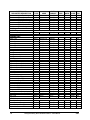
ANALOG OUTPUT DATA
ANALOG OUTPUT
PARAMETER DESCRIPTION
INPUTS:
AO: Input Source/Set Point
AO: Slidewire
OUTPUTS:
AO: Output Value
PARAMETERS:
AO Card Type
AO Card Type
AO: Count
AO: Decreasing Slew Rate Limit
AO: Drive Unit Sensitivity
AO: Drive Unit Speed
AO: Failsafe/Preset 1 Value
AO: Failsafe/Preset Value
AO: Function Block Description
AO: Function Block Description
AO: Function Block Tag
AO: Impulse Time
AO: Increasing Slew Rate Limit
AO: Minimum OFF Time
AO: Minimum ON Time
AO: Output Decreasing
AO: Output High Limit
AO: Output Increasing
AO: Output Low Limit
AO: Process Variable High Lim
AO: Process Variable Low Lim
AO: Slew Rate Time
TYPE
ADDR
DATA
FORMAT
SIZE
R/W
MODE
UNIT
CODE
PG.
0x3D
0x3F
0x01-xx
0x01-xx
FLOAT
FLOAT
4
4
R
R
S,M,P
M,P
80
80
0x3E
0x01-xx
FLOAT
4
R
S,M,P
80
0x02
0x02
0x02
0x4C
0x46
0x70
0x4A
0x36
0xC1
0xD7
0xC7
0x42
0x45
0x44
0x43
0x6F
0x90
0x6E
0x91
0x40
0x41
0x45
0x12-0x19
0x34-0x3B
0x52
0x01-xx
0x01-xx
0x01-xx
0x01-xx
0x01-xx
0x01-xx
0x01-xx
0x01-xx
0x01-xx
0x01-xx
0x01-xx
0x01-xx
0x01-0x10
0x01-xx
0x01-0x10
0x01-xx
0x01-xx
0x01-xx
0x01-0x10
BINARY
BINARY
BINARY
FLOAT
FLOAT
FLOAT
FLOAT
FLOAT
TEXT
TEXT
TEXT
FLOAT
FLOAT
FLOAT
FLOAT
BINARY
FLOAT
BINARY
FLOAT
FLOAT
FLOAT
FLOAT
1
1
2
4
4
4
4
4
14
16
7
4
4
4
4
1
4
1
4
4
4
4
R
R
R
RW
RW
RW
RW
RW
RW
RW
RW
RW
RW
RW
RW
R
RW
R
RW
RW
RW
RW
M
S
P
P
M,P
M,P
M,P
P
S,P
P
S,P
M,P
P
M,P
M,P
M
S,M,P
M
S,M,P
S,M,P
S,M,P
M
59
65
66
81
81
85
81
79
92
94
93
80
80
80
80
85
88
85
88
80
80
80
R/W
MODE
UNIT
CODE
PG.
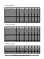
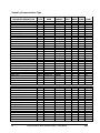
CONSTANT PARAMETERS
CONSTANT
PARAMETER DESCRIPTION
OUTPUTS:
CN: Value
PARAMETERS:
CN: Count
CN: Function Block Description
CN: Function Block Description
CN: Function Block Tag
CN: Packet 1-200
CN: Packet 1-25 (Recipe #1)
CN: Packet 101-125 (Recipe #3)
CN: Packet 126-150 (Recipe #4)
CN: Packet 151-200
CN: Packet 26-50 (Recipe #2)
5/99
TYPE
ADDR
DATA
FORMAT
SIZE
0x25
0x01-xx
FLOAT
4
RW
S,M,P
77
0x02
0xC3
0xD9
0xC9
0x17
0x17
0x17
0x17
0x17
0x17
0x55
0x01-xx
0x01-xx
0x01-xx
0x06
0x00
0x03
0x04
0x05
0x01
BINARY
TEXT
TEXT
TEXT
BLOCK
BLOCK
BLOCK
BLOCK
BLOCK
BLOCK
2
14
16
7
800
100
100
100
200
100
R
RW
RW
RW
RW
RW
RW
RW
RW
RW
P
S,P
P
S,P
M
M
M
M
M
M
66
92
94
93
71
71
71
71
71
71
Honeywell Binary Serial Communications – User Manual
33
CONSTANT
PARAMETER DESCRIPTION
CN: Packet 51-100
TYPE
0x17
ADDR
0x02
DATA
FORMAT
BLOCK
SIZE
200
R/W
MODE
RW
UNIT
CODE
M
PG.
71
TYPE
ADDR
DATA
FORMAT
SIZE
R/W
MODE
UNIT
CODE
PG.
CONTROL RELAY DATA
CONTROL RELAY
PARAMETER DESCRIPTION
OUTPUTS:
CR: Control Relays Output
PARAMETERS:
CR: Block 2
CR: Block 3
CR: Block 4
CR: Packet 9 – CR: 1-999 Output
0x7B
0x01-0xFF
BINARY
1
R
M
86
0x7C
0x7D
0x7E
0x19
0x00-0xFF
0x00-0xFF
0x00-0xE7
0x08
BINARY
BINARY
BINARY
BLOCK
1
1
1
134
R
R
R
R
M
M
M
M
87
87
87
74
R/W
MODE
UNIT
CODE
PG.
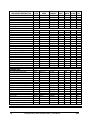
CALCULATED VALUE/PSEUDO POINT DATA
CALC’D VALUE/PSEUDO POINT
PARAMETER DESCRIPTION
INPUTS:
CV: Back Calc Input Value
OUTPUTS:
CV/PP: Output Value (256-511)
CV:/PP: Output Status
CV:/PP: Output Status 2
CV:/PP: Output Status 3
CV:/PP: Output Status 4
CV:/PP: Output Value (1-255)
PARAMETERS:
CV: Count
CV:/PP: Engineering Units Text
CV:/PP: Engineering Units Text
CV:/PP: Function Block Descr.
CV:/PP: Function Block Descr.
CV:/PP: Function Block Tag
CV:/PP: Limit Clamp
CV:/PP: Output High Limit
CV:/PP: Output High Limit
CV:/PP: Output Low Limit
CV:/PP: Output Low Limit
CV:/PP: Packet 2 – CV/PP Output
CV:/PP: Packet 2 – CV/PP Output
CV:/PP: Packet 3 – CV/PP Output
34
TYPE
ADDR
DATA
FORMAT
SIZE
0x48
0x01-xx
FLOAT
4
R
P
81
0x1F
0x85
0x87
0x89
0x8B
0x1E
0x01-0xFF
0x01-xx
0x01-xx
0x01-xx
0x01-xx
0x01-xx
FLOAT
BINARY
BINARY
BINARY
BINARY
FLOAT
4
1
1
1
1
4
R
R
R
R
R
R
M
S,M,P
S,M
S,M
S,M
S,M,P
76
87
87
87
88
76
0x02
0xCD
0xCD
0xC2
0xD8
0xC8
0x8D
0x49
0x49
0x4B
0x4B
0x19
0x19
0x19
0x59
0x01-0x3C
0x01-xx
0x01-xx
0x01-xx
0x01-xx
0x01-xx
0x01-xx
0x01-xx
0x01-xx
0x01-xx
0x01
0x13
0x02
BINARY
TEXT
TEXT
TEXT
TEXT
TEXT
BINARY
FLOAT
FLOAT
FLOAT
FLOAT
BLOCK
BLOCK
BLOCK
2
6
6
14
16
7
1
4
4
4
4
1016
240
1020
R
RW
R
RW
RW
RW
R
RW
R
RW
R
R
R
R
P
S
P
S,P
P
S,P
S,M
S,M
P
S,M
P
M
S
M
67
93
93
92
94
93
88
81
81
81
81
72
74
72
Honeywell Binary Serial Communications – User Manual
5/99
DIGITAL INPUT DATA
DIGITAL INPUT
PARAMETER DESCRIPTION
OUTPUTS:
DI: Output Status
PARAMETERS:
DI: Count
DI: Function Block Description
DI: Function Block Description
DI: Function Block Tag
DI: Off Label Text
DI: Off Label Text
DI: On Label Text
DI: On Label Text
DI: On/Off Label Text
DI: Packet 7 – DI Output
DI: Packet 7 – DI Output
TYPE
ADDR
DATA
FORMAT
SIZE
R/W
MODE
UNIT
CODE
PG.
0x21
0x01-xx
BINARY
1
RW
S,M,P
76
0x02
0xC4
0xDA
0xCA
0xD0
0xD0
0xCE
0xCE
0xD2
0x19
0x19
0x53
0x01-xx
0x01-xx
0x01-xx
0x01-0x87
0x01-xx
0x01-0x87
0x01-xx
0x01-xx
0x06
0x17
BINARY
TEXT
TEXT
TEXT
TEXT
TEXT
TEXT
TEXT
TEXT
BLOCK
BLOCK
2
14
16
7
6
6
6
6
6
30
18
R
RW
RW
RW
RW
R
RW
R
R
R
R
P
S,P
P
S,P
S
P
S
P
S,P
M
S
66
93
95
93
94
94
93
93
94
73
75
R/W
MODE
UNIT
CODE
PG.
DIGITAL OUTPUT DATA
DIGITAL OUTPUT
PARAMETER DESCRIPTION
OUTPUTS:
DO: Output Status
PARAMETERS:
DO: Count
DO: Function Block Description
DO: Function Block Description
DO: Function Block Tag
DO: Off Label Text
DO: Off Label Text
DO: On Label Text
DO: On Label Text
DO: On/Off Label Text
DO: Packet 8 – DO Output
DO: Packet 8 – DO Output
TYPE
ADDR
DATA
FORMAT
SIZE
0x23
0x01-xx
BINARY
1
RW
S,M,P
76
0x02
0xC5
0xDB
0xCB
0xD1
0xD1
0xCF
0xCF
0xD3
0x19
0x19
0x54
0x01-xx
0x01-xx
0x01-xx
0x01-0x87
0x01-xx
0x01-0x87
0x01-xx
0x01-xx
0x07
0x18
BINARY
TEXT
TEXT
TEXT
TEXT
TEXT
TEXT
TEXT
TEXT
BLOCK
BLOCK
2
14
16
7
6
6
6
6
6
30
18
R
RW
RW
RW
RW
R
RW
R
R
R
R
P
S,P
P
S,P
S
P
S
P
S,P
M
S
66
93
95
93
94
94
94
94
94
73
75
R/W
MODE
UNIT
CODE
PG.
R
R
R
R
R
M
M
M
M
M
89
89
89
89
89
CONTROL LOOP DATA
CONTROL LOOP
PARAMETER DESCRIPTION
INPUTS:
LP: Carbon; CO Compensation
LP: Carbon; Furnace Factor
LP: Carbon; Furnace Temp
LP: Carbon; Optional Selection
LP: Carbon; Sensor
5/99
TYPE
0x98
0x99
0x97
0x9A
0x96
ADDR
0x01-0x10
0x01-0x10
0x01-0x10
0x01-0x10
0x01-0x10
DATA
FORMAT
FLOAT
FLOAT
FLOAT
BINARY
FLOAT
SIZE
4
4
4
1
4
Honeywell Binary Serial Communications – User Manual
35
CONTROL LOOP
PARAMETER DESCRIPTION
LP: Control Feedback 1 Value
LP: Control Feedback 2 Value
LP: Control Feedback Value
LP: Local Set Point (SP1)
LP: Process Variable
LP: Remote Set Point (SP2)
LP: Self Tune Process Variable
OUTPUTS:
LP: Back Calc Output Value
LP: Cascade Status
LP: Control Action Selection
LP: Control Action Status
LP: Control Auto/Manual Status
LP: Control Auto/Manual Status
LP: Deviation
LP: Integral Hold Status
LP: Manual Output Value
LP: Output 1
LP: Output 2
LP: Output ON/OFF Status
LP: Output ON/OFF Status
LP: Output Value
LP: Output Value
LP: Set Point Status
LP: Set Point Status
LP: Tuning Parameter Status
LP: Windup Status
LP: Working Set Point
LP: Working Set Point (%)
PARAMETERS:
LP: Approach Value High
LP: Approach Value Low
LP: Bias (P: Manual Reset)
LP: Bias 1 (P: Manual Reset)
LP: Bias 2
LP: Cascade 1 Select
LP: Cascade 2 Select
LP: Control Action Change
LP: Control Auto/Man Selection
LP: Control Auto/Man Selection
LP: Control Forceback
LP: Control Output Force Manual
LP: Control Preset Output (PID)
LP: Count
LP: Deadband
LP: Decreasing Slew Rate Limit
LP: Error Square
LP: Feed Forward Value
LP: Force Bumpless Trnsfr Select
LP: Force Local Set Point
36
TYPE
0x47
0x48
0x38
0x04
0x03
0x05
0x67
ADDR
0x01-xx
0x01-0x10
0x01-xx
0x01-xx
0x01-xx
0x01-xx
0x01-0x10
DATA
FORMAT
FLOAT
FLOAT
FLOAT
FLOAT
FLOAT
FLOAT
FLOAT
SIZE
4
4
4
4
4
4
4
R/W
MODE
R
R
R
RW
R
RW
R
UNIT
CODE
M,P
M
M,P
M,P
M,P
M,P
M
PG.
81
81
79
68
67
68
84
0x31
0x5B
0x59
0x58
0x55
0x55
0x06
0x60
0x3C
0x69
0x6A
0x66
0x66
0x08
0x08
0x52
0x52
0x64
0x5E
0x2D
0x6B
0x01-xx
0x01-0x10
0x01-xx
0x01-xx
0x01-0x10
0x01-xx
0x01-xx
0x01-0x10
0x01-xx
0x01-xx
0x01-0x10
0x01-0x10
0x01-xx
0x01-0x10
0x01-xx
0x01-0x10
0x01-xx
0x01-xx
0x01-0x10
0x01-xx
0x01-0x10
FLOAT
BINARY
BINARY
BINARY
BINARY
BINARY
FLOAT
BINARY
FLOAT
FLOAT
FLOAT
BINARY
BINARY
FLOAT
FLOAT
BINARY
BINARY
BINARY
BINARY
FLOAT
FLOAT
4
1
1
1
1
1
4
1
4
4
4
1
1
4
4
1
1
1
1
4
4
R
R
W
R
R
RW
R
R
RW
RW
RW
R
RW
R
RW
R
RW
R
R
R
RW
M,P
M
M,P
M,P
M
P
M,P
M
M,P
M,P
M
M
P
M
P
M
P
M,P
M
M,P
M
79
83
83
82
82
82
68
83
80
84
84
84
84
68
68
82
82
84
83
78
84
0x0F
0x10
0x33
0x62
0x68
0x5C
0x5D
0x5A
0x56
0x56
0x39
0x57
0x36
0x02
0x3B
0x30
0x35
0x37
0x61
0x54
0x01-xx
0x01-xx
0x01-xx
0x01-xx
0x01-0x10
0x01-0x10
0x01-0x10
0x01-xx
0x01-0x10
0x01-xx
0x01-0x10
0x01-xx
0x01-0x10
0x58
0x01-xx
0x01-xx
0x01-0x10
0x01-xx
0x01-0x10
0x01-0x10
FLOAT
FLOAT
FLOAT
FLOAT
FLOAT
BINARY
BINARY
BINARY
BINARY
BINARY
FLOAT
BINARY
FLOAT
BINARY
FLOAT
FLOAT
FLOAT
FLOAT
BINARY
BINARY
4
4
4
4
4
1
1
1
1
1
4
1
4
2
4
4
4
4
1
1
RW
RW
RW
RW
RW
R
R
R
W
RW
RW
R
RW
R
RW
RW
RW
RW
RW
R
M,P
M,P
P
M,P
M
M
M
M,P
M
P
M
M,P
M
P
M,P
P
M
M,P
M
M
68
69
79
84
84
83
83
83
82
82
80
82
79
67
80
79
79
79
83
82
Honeywell Binary Serial Communications – User Manual
5/99
CONTROL LOOP
PARAMETER DESCRIPTION
LP: Force Off Select
LP: Function Block Description
LP: Function Block Tag
LP: Gain 1
LP: Gain 2
LP: Increasing Slew Rate Limit
LP: Integral Hold Selection
LP: Local SP Engineering Units
LP: Manual Reset
LP: PID Loop Type
LP: Process Variable High Limit
LP: Process Variable Low Limit
LP: Rate 1
LP: Rate 2
LP: Ratio
LP: Reset 1
LP: Reset 2
LP: Reset Limit
LP: Set Point Selection
LP: Set Point Selection
LP: Set Point Slew Rate
LP: Set Point Tracking
LP: Tuning Parameter Selection
LP: Wild Variable
LP: Working Set Point High Limit
LP: Working Set Point Low Limit
TYPE
0x65
0xDC
0xD4
0x0B
0x09
0x22
0x5F
0x32
0x33
0x6D
0x2B
0x2C
0x0D
0x3A
0x6C
0x0C
0x0A
0x34
0x53
0x53
0x30
0xA0
0x63
0x0E
0x2E
0x2F
ADDR
0x01-0x10
0x01-xx
0x01-xx
0x01-xx
0x01-xx
0x01-xx
0x01-0x10
0x01-xx
0x01-0x10
0x01-xx
0x01-xx
0x01-xx
0x01-xx
0x01-xx
0x01-xx
0x01-xx
0x01-xx
0x01-xx
0x01-0x10
0x01-xx
0x01-0x10
0x01-xx
0x01-xx
0x01-xx
0x01-xx
0x01-xx
DATA
FORMAT
BINARY
TEXT
TEXT
FLOAT
FLOAT
FLOAT
BINARY
FLOAT
FLOAT
BINARY
FLOAT
FLOAT
FLOAT
FLOAT
FLOAT
FLOAT
FLOAT
FLOAT
BINARY
BINARY
FLOAT
BINARY
BINARY
FLOAT
FLOAT
FLOAT
SIZE
1
16
7
4
4
4
1
4
4
2
4
4
4
4
4
4
4
4
1
1
4
1
1
4
4
4
R/W
MODE
RW
RW
RW
RW
RW
RW
RW
R
RW
R
RW
RW
RW
RW
RW
RW
RW
RW
W
RW
RW
R
RW
R
RW
RW
UNIT
CODE
M
P
P
M,P
M,P
P
M
M,P
M
M,P
M,P
M,P
M,P
M,P
M,P
M,P
M,P
M,P
M
P
M
M,P
M,P
M,P
M,P
M,P
PG.
84
95
94
68
68
76
83
79
79
84
78
78
68
80
84
68
68
79
82
82
79
90
84
68
78
79
DATA
FORMAT
SIZE
R/W
MODE
UNIT
CODE
PG.
PLC DATA
PLC
PARAMETER DESCRIPTION
INPUTS:
PLC: Counter Count Input
PLC: Counter Preset Value
PLC: Counter Reset Input
PLC: Drum Advance Step Input
PLC: Drum Jog Input
PLC: Drum Reset Input
PLC: Drum Run/Hold Input
PLC: Timer Preset Value
PLC: Timer Reset Input
PLC: Timer Time Input
OUTPUTS:
PLC: Run Status
PLC: Counter Current Value
PLC: Counter Down/Up
PLC: Drum 2 Outputs
PLC: Drum 3 Outputs
PLC: Drum 4 Outputs
5/99
TYPE
ADDR
0xA3
0x82
0xA5
0xA8
0xA7
0xA9
0xA6
0x80
0xA2
0xA1
0x01-0x50
0x01-0x50
0x01-0x50
0x01-0x04
0x01-0x04
0x01-0x04
0x01-0x04
0x01-0x50
0x01-0x50
0x01-0x50
BINARY
FLOAT
BINARY
BINARY
BINARY
BINARY
BINARY
FLOAT
BINARY
BINARY
1
4
1
1
1
1
1
4
1
1
R
RW
R
R
R
R
R
RW
R
R
M
M
M
M
M
M
M
M
M
M
91
87
91
91
91
91
91
87
91
90
0xAC
0x81
0xA4
0xBC
0xBD
0xBE
0x01
0x01-0x50
0x01-0x50
0x01-0x10
0x01-0x10
0x01-0x10
BINARY
FLOAT
BINARY
BINARY
BINARY
BINARY
1
4
1
1
1
1
R
R
R
R
R
R
M
M
M
M
M
M
91
87
91
92
92
92
Honeywell Binary Serial Communications – User Manual
37
PLC
PARAMETER DESCRIPTION
PLC: Drum Outputs (packed)
PLC: Drum Outputs (single)
PLC: Drum Step Number
PLC: Drum Step Time
PLC: MCR Coil Status
PLC: Skip Coil Status
PLC: Timer Current Value
PARAMETERS:
PLC: Drum Jog
TYPE
0x71
0x8F
0x83
0x84
0xAA
0xAB
0x7F
ADDR
0x01-0x04
0x01-0x10
0x01-0x04
0x01-0x04
0x00
0x01
0x01-0x50
DATA
FORMAT
BINARY
BINARY
FLOAT
FLOAT
BINARY
BINARY
FLOAT
SIZE
2
1
4
4
1
1
4
R/W
MODE
R
R
RW
RW
R
R
R
UNIT
CODE
M
M
M
M
M
M
M
PG.
85
88
87
87
91
91
87
0x92
0x01-0x04
FLOAT
4
R
M
88
R/W
MODE
UNIT
CODE
PG.
SET POINT PROGRAMMER DATA
SETPOINT PROGRAMMER
PARAMETER DESCRIPTION
OUTPUTS:
SPP: #1 Current Events
SPP: #2 Current Events
SPP: #3 Current Events
SPP: #4 Current Events
SPP: Current Step Number
SPP: Output Value
SPP: Program Elapsed Time
SPP: Status
SPP: Step Time Remaining
PARAMETERS:
SPP: #1 Current Recipe Index
SPP: #2 Current Recipe Index
SPP: #3 Current Recipe Index
SPP: #4 Current Recipe Index
SPP: Advance
SPP: Count
SPP: Events (packed)
SPP: Function Block Description
SPP: Function Block Tag
SPP: Hold
SPP: Jog
SPP: Jog to Segment
SPP: Reset
SPP: Start
SPP: #1 Step Duration/Time
SPP: #1 Step Value
SPP: #2 Step Duration/Time
SPP: #2 Step Value
SPP: #3 Step Duration/Time
SPP: #3 Step Value
SPP: #4 Step Duration/Time
SPP: #4 Step Value
SPP: Time
38
TYPE
ADDR
DATA
FORMAT
SIZE
0x79
0x7A
0x26
0x27
0x50
0x4D
0x4E
0x78
0x4F
0x01-0x10
0x01-0x10
0x01-0x10
0x01-0x10
0x01-xx
0x01-xx
0x01-xx
0x01-xx
0x01-xx
BINARY
BINARY
BINARY
BINARY
FLOAT
FLOAT
FLOAT
BINARY
FLOAT
1
1
1
1
4
4
4
1
4
R
R
R
R
R
R
R
R
R
M,P
M,P
M,P
M,P
M,P
M,P
M,P
M,P
M,P
86
86
77
77
81
81
81
86
81
0x9F
0x9F
0x9F
0x9F
0x76
0x02
0x9D
0xDD
0xD5
0x75
0x77
0x51
0x74
0x73
0x8A
0x88
0x8E
0x8C
0x24
0x1B
0xE7
0xE6
0x72
0x00
0x01
0x02
0x03
0x01-xx
0x57
0x01-xx
0x01-xx
0x01-xx
0x01-xx
0x01-xx
0x01-xx
0x01-xx
0x01-xx
0x01-0x3F
0x01-0x3F
0x01-0x3F
0x01-0x3F
0x01-0x3F
0x01-0x3F
0x01-0x3F
0x01-0x3F
0x01-xx
FLOAT
FLOAT
FLOAT
FLOAT
BINARY
BINARY
BINARY
TEXT
TEXT
BINARY
BINARY
FLOAT
BINARY
BINARY
FLOAT
FLOAT
FLOAT
FLOAT
FLOAT
FLOAT
FLOAT
FLOAT
BINARY
4
4
4
4
1
2
2
16
7
1
1
4
1
1
4
4
4
4
4
4
4
4
3
R
R
R
R
W
R
R
RW
RW
W
W
R
W
W
RW
RW
RW
RW
RW
RW
RW
RW
R
M
M
M
M
M,P
P
M,P
P
P
M,P
M
M
M,P
M,P
P
P
P
P
P
P
P
P
M
90
90
90
90
86
67
90
95
94
86
86
82
86
85
88
87
88
88
77
76
96
96
85
Honeywell Binary Serial Communications – User Manual
5/99
SELF TUNE DATA
SELF TUNE
PARAMETER DESCRIPTION
INPUTS:
Self Tune: Hold Input
OUTPUTS:
Self Tune: % Complete
PARAMETERS:
Self Tune: Advance
Self Tune: Current Gain
Self Tune: Current Rate
Self Tune: Current Reset
Self Tune: Hold
Self Tune: Optune Gain
Self Tune: Optune Rate
Self Tune: Optune Reset
Self Tune: Reset
Self Tune: Start
Self Tune: Status
TYPE
ADDR
DATA
FORMAT
SIZE
R/W
MODE
UNIT
CODE
PG.
0xB9
0x01
BINARY
1
R
M
92
0xB8
0x01
FLOAT
4
R
M
92
0xB6
0xAD
0xAE
0xAF
0xB5
0xB0
0xB1
0xB2
0xB4
0xB3
0xB7
0x01
0x01
0x01
0x01
0x01
0x01
0x01
0x01
0x01
0x01
0x01
BINARY
FLOAT
FLOAT
FLOAT
BINARY
FLOAT
FLOAT
FLOAT
BINARY
BINARY
BINARY
1
4
4
4
1
4
4
4
1
1
1
RW
R
R
R
RW
R
R
R
RW
RW
R
M
M
M
M
M
M
M
M
M
M
M
92
91
91
91
92
91
91
91
92
92
92
R/W
MODE
UNIT
CODE
PG.
SYSTEM/UNIT DATA
SYSTEM/UNIT
PARAMETER DESCRIPTION
COMMUNICATIONS:
Comm Configuration
Local Station Link Status
Main/Port A Comm Address
Main/Port A Comm Configuration
Optional/Port B Comm Address
Optional/Port B Comm Config.
Port A Baud Rate
Port A Unit Address
Port B Baud Rate
Port B Unit Address
Security Code – Comm Channels
DIAGNOSTICS:
AI: Calibration
AO: Calibration
Copy Block (AI)
Decrement/Escape
Diagnostic Display
Diagnostic Error Status
Enter
Increment/Advance
Mode DIP Switch
5/99
TYPE
ADDR
DATA
FORMAT
SIZE
0x02
0X02
0x02
0X02
0X02
0X02
0x02
0x02
0x02
0x02
0x02
0x1A
0x2A
0x22
0x23
0x24
0x25
0x41
0x40
0x43
0x42
0x44
BINARY
BINARY
BINARY
BINARY
BINARY
BINARY
BINARY
BINARY
BINARY
BINARY
BINARY
1
6
1
1
1
1
1
1
1
1
8
RW
RW
R
R
R
R
R
R
R
R
RW
M,P
M
S,M
S,M
S,M
S,M
M
M
M
M
M
59
63
61
61
62
62
66
66
66
66
66
0x02
0x02
0x02
0x02
0x00
0x14
0x02
0x02
0x02
0x2B
0x2C
0x45
0x1E
0x01
0x01-xx
0x1D
0x1F
0x21
BINARY
BINARY
BINARY
BINARY
TEXT
BINARY
BINARY
BINARY
BINARY
3
3
4
1
16
1
1
1
1
W
W
W
W
R
R
W
W
R
P
P
P
M,P
S,M
S,M
M,P
M,P
S,M
64
64
66
60
56
69
60
60
61
Honeywell Binary Serial Communications – User Manual
39
SYSTEM/UNIT
PARAMETER DESCRIPTION
Rack Loading AL: Time Usage
Rack Loading Free Space
Rack Loading PLC Free Space
Rack Loading PLC Time Usage
Rack Loading PP: Time Usage
Rack Loading Time Units
Rack Loading Time Usage
Slot Diagnostics
OUTPUTS:
Reference Temperature
Program Number
PARAMETERS:
Card Type
Chart Mode
Chart Speed 1
Chart Speed 2
Chart Speed Select
Chart Status
Clock
Configuration Download
Configuration Index
Configuration Upload
Configuration Upload
CPU Type
Database Programming
Dynamic Packet Definition
Dynamic Packet Definition
Dynamic Packet/Block Access
Dynamic Packet/Block Access
Firmware Part Number
Local Relays
Local Time
Mains Frequency
Packet 10 - Card Types
Packet 10 - Card Types
Packet 11 - Diagnostics
Packet 11 - Diagnostics
Packet 4 - Simple Poll
Rack Card Type
Rack Card Type
Response Queue
Security Access Groups - Local
Security Access Groups - PMC
Unit Type
Update Rate
STATUS:
Data Base Status
Local Station 1 Storage
Local Station 2 Storage
Operation Status
40
TYPE
0x94
0x94
0x94
0x94
0x94
0x94
0x94
0x93
ADDR
0x04
0x01
0x06
0x05
0x03
0x07
0x02
0x01-0x0F
DATA
FORMAT
FLOAT
FLOAT
FLOAT
FLOAT
FLOAT
FLOAT
FLOAT
BINARY
SIZE
4
4
4
4
4
4
4
1
R/W
MODE
R
R
R
R
R
R
R
R
UNIT
CODE
M
M
M
M
M
M
S,M
M
PG.
89
88
89
89
89
89
88
88
0x16
0x02
0x01-0xxx
0x2E
FLOAT
FLOAT
4
4
R
RW
P
P
71
64
0X02
0x02
0x02
0x02
0x02
0x02
0x02
0x02
0x02
0x02
0x02
0x02
0x20
0x29
0x29
0x2A
0x2A
0x01
0X02
0x1D
0x02
0x19
0x19
0x19
0x19
0x19
0x02
0x02
0x9E
0x02
0x02
0x00
0x02
0x2B-0x33
0x3C
0x3D
0x3E
0x3F
0x40
0x2F
0xC0
0x2D
0xC1
0xC2
0x65
0x00
0x00-0x04
0x04
0x00-0x04
0x04
0x00-0x03
0x27
0x00
0x30
0x09
0x19
0x0A
0x1A
0x03
0x03-0x11
0x-03-0x12
0x00
0x1C
0x1B
0x00
0x01
BINARY
BINARY
FLOAT
FLOAT
BINARY
BINARY
BINARY
TEXT
BINARY
BINARY
TEXT
BINARY
----------TEXT
BINARY
BINARY
BINARY
BLOCK
BLOCK
BLOCK
BLOCK
BLOCK
BINARY
BINARY
BINARY
BINARY
BINARY
TEXT
BINARY
1
1
4
4
1
1
7
--1
----1
----------16
1
3
1
23
17
23
60
26-326
1
1
1-301
1
1
16
1
R
R
R
R
RW
RW
RW
W
W
W
R
R
RW
RW
RW
RW
RW
R
RW
RW
RW
R
R
R
R
R
R
R
R
RW
RW
R
R
S
S
S
S
S
S
P
P
P
P
P
P
S,M
S,M
P
S,M
P
M,P
M
S,M,P
P
M
S
M
S
S,M,P
M
P
S,M
M
M
S,M,P
S,M,P
63
65
65
65
65
66
65
97
64
98
98
67
76
78
78
78
78
56
62
75
65
74
75
74
75
72
58
58
90
60
59
56
57
0X02
0X02
0X02
0x02
0x26
0x28
0x29
0x20
BINARY
BINARY
BINARY
BINARY
2
6
6
1
RW
RW
RW
W
M
M
M
S,M
62
62
62
60
Honeywell Binary Serial Communications – User Manual
5/99
SYSTEM/UNIT
PARAMETER DESCRIPTION
Operation Status
Profile Count
System Status
TYPE
0x02
0x02
0x02
ADDR
0x20
0x63
0x00
DATA
FORMAT
BINARY
BINARY
BINARY
SIZE
1
2
4
R/W
MODE
RW
R
R
UNIT
CODE
P
P
S,M,P
PG.
60
67
56
TYPE
ADDR
DATA
FORMAT
SIZE
R/W
MODE
UNIT
CODE
PG.
TOTALIZER DATA
TOTALIZER
PARAMETER DESCRIPTION
OUTPUTS:
TL: Output Status
TL: Output Value
PARAMETERS:
TL: Count
TL: Engineering Units Text
TL: Function Block Description
TL: Function Block Tag
5/99
0x86
0x1C
0x01-xx
0x01-xx
BINARY
FLOAT
1
4
R
R
P
P
87
76
0x02
0xE0
0xDE
0xDF
0x60
0x01-xx
0x01-xx
0x01-xx
BINARY
TEXT
TEXT
TEXT
2
6
16
7
R
R
RW
RW
P
P
P
P
67
95
95
95
Honeywell Binary Serial Communications – User Manual
41
Sorted by Communication Type
PARAMETER DESCRIPTION
Unit Type
Diagnostic Display
Firmware Part Number
System Status
Update Rate
Rack Card Type
Rack Card Type
AO Card Type
Comm Configuration
Security Access Groups - PMC
Security Access Groups - Local
Enter
Decrement/Escape
Increment/Advance
Operation Status
Operation Status
Mode DIP Switch
Main/Port A Comm Address
Main/Port A Comm Configuration
Optional/Port B Comm Address
Optional/Port B Comm Config.
Data Base Status
Local Relays
Local Station 1 Storage
Local Station 2 Storage
Local Station Link Status
Card Type
AI: Calibration
AO: Calibration
Configuration Index
Program Number
Clock
Mains Frequency
AO Card Type
Chart Mode
Chart Speed 1
Chart Speed 2
Chart Speed Select
Chart Status
Port A Unit Address
Port A Baud Rate
Port B Unit Address
Port B Baud Rate
Security Code - Comm Channels
Copy Block (AI)
AI: Count
AO: Count
DI: Count
DO: Count
42
TYPE
0x00
0x00
0x01
0x02
0x02
0x02
0x02
0x02
0x02
0x02
0x02
0x02
0x02
0x02
0x02
0x02
0x02
0x02
0X02
0X02
0X02
0X02
0X02
0X02
0X02
0X02
0X02
0x02
0x02
0x02
0x02
0x02
0x02
0x02
0x02
0x02
0x02
0x02
0x02
0x02
0x02
0x02
0x02
0x02
0x02
0x02
0x02
0x02
0x02
ADDR
0x00
0x01
0x00-0x03
0x00
0x01
0x03-0x11
0x03-0x12
0x12-0x19
0x1A
0x1B
0x1C
0x1D
0x1E
0x1F
0x20
0x20
0x21
0x22
0x23
0x24
0x25
0x26
0x27
0x28
0x29
0x2A
0x2B-0x33
0x2B
0x2C
0x2D
0x2E
0x2F
0x30
0x34-0x3B
0x3C
0x3D
0x3E
0x3F
0x40
0x40
0x41
0x42
0x43
0x44
0x45
0x51
0x52
0x53
0x54
DATA
FORMAT
TEXT
TEXT
TEXT
BINARY
BINARY
BINARY
BINARY
BINARY
BINARY
BINARY
BINARY
BINARY
BINARY
BINARY
BINARY
BINARY
BINARY
BINARY
BINARY
BINARY
BINARY
BINARY
BINARY
BINARY
BINARY
BINARY
BINARY
BINARY
BINARY
BINARY
FLOAT
BINARY
BINARY
BINARY
BINARY
FLOAT
FLOAT
BINARY
BINARY
BINARY
BINARY
BINARY
BINARY
BINARY
BINARY
BINARY
BINARY
BINARY
BINARY
SIZE
16
16
16
4
1
1
1
1
1
1
1
1
1
1
1
1
1
1
1
1
1
2
1
6
6
6
1
3
3
1
4
7
1
1
1
4
4
1
1
1
1
1
1
8
4
2
2
2
2
Honeywell Binary Serial Communications – User Manual
R/W
MODE
R
R
R
R
R
R
R
R
RW
RW
RW
W
W
W
W
RW
R
R
R
R
R
RW
RW
RW
RW
RW
R
W
W
W
RW
RW
RW
R
R
R
R
RW
RW
R
R
R
R
RW
W
R
R
R
R
UNIT
CODE
S,M,P
S,M
M,P
S,M,P
S,M,P
M
P
M
M,P
M
M
M,P
M,P
M,P
S,M
P
S,M
S,M
S,M
S,M
S,M
M
M
M
M
M
S
P
P
P
P
P
P
S
S
S
S
S
S
M
M
M
M
M
P
P
P
P
P
PAGE
56
56
56
56
57
58
58
59
59
59
60
60
60
60
60
60
61
61
61
62
62
62
62
62
62
63
63
64
64
64
64
65
65
65
65
65
65
65
66
66
66
66
66
66
66
66
66
66
66
5/99
PARAMETER DESCRIPTION
CN: Count
AL: Count
SPP: Count
LP: Count
CV: Count
TL: Count
Profile Count
CPU Type
Configuration Download
Configuration Upload
Configuration Upload
LP: Process Variable
LP: Local Set Point (SP1)
LP: Remote Set Point (SP2)
LP: Deviation
AI: Output Value
LP: Output Value
LP: Output Value
LP: Gain 2
LP: Reset 2
LP: Gain 1
LP: Reset 1
LP: Rate 1
LP: Wild Variable
LP: Approach Value High
LP: Approach Value Low
AL: Set Point
AL: Output Status
AL: Hysteresis
AL: Hysteresis
Diagnostic Error Status
AI: Adjustment Value
SY: Reference Temperature
CN: Packet 1-25 (Recipe #1)
CN: Packet 26-50 (Recipe #2)
CN: Packet 51-100
CN: Packet 101-125 (Recipe #3)
CN: Packet 126-150 (Recipe #4)
CN: Packet 151-200
CN: Packet 1-200
AI: Packet 1 - AI Output
CV:/PP: Packet 2 - CV/PP Output
CV:/PP: Packet 3 - CV/PP Output
Packet 4 - Simple Poll
AL: Packet 5 - AL Status Packed
AI: Packet 6 - AI Status
DI: Packet 7 - DI Output
DO: Packet 8 - DO Output
CR: Packet 9 - CR: 1-999 Output
Packet 10 - Card Types
Packet 11 - Diagnostics
5/99
TYPE
0x02
0x02
0x02
0x02
0x02
0x02
0x02
0x02
0x02
0x02
0x02
0x03
0x04
0x05
0x06
0x07
0x08
0x08
0x09
0x0A
0x0B
0x0C
0x0D
0x0E
0x0F
0x10
0x11
0x12
0x13
0x13
0x14
0x15
0x16
0x17
0x17
0x17
0x17
0x17
0x17
0x17
0x19
0x19
0x19
0x19
0x19
0x19
0x19
0x19
0x19
0x19
0x19
ADDR
0x55
0x56
0x57
0x58
0x59
0x60
0x63
0x65
0xC0
0xC1
0xC2
0x01-xx
0x01-xx
0x01-xx
0x01-xx
0x01-xx
0x01-0x10
0x01-xx
0x01-xx
0x01-xx
0x01-xx
0x01-xx
0x01-xx
0x01-xx
0x01-xx
0x01-xx
0x01-xx
0x01-xx
0x00
0x01-xx
0x01-xx
0x01-xx
0x01
0x00
0x01
0x02
0x03
0x04
0x05
0x06
0x00
0x01
0x02
0x03
0x04
0x05
0x06
0x07
0x08
0x09
0x0A
DATA
FORMAT
BINARY
BINARY
BINARY
BINARY
BINARY
BINARY
BINARY
BINARY
TEXT
BINARY
TEXT
FLOAT
FLOAT
FLOAT
FLOAT
FLOAT
FLOAT
FLOAT
FLOAT
FLOAT
FLOAT
FLOAT
FLOAT
FLOAT
FLOAT
FLOAT
FLOAT
BINARY
FLOAT
FLOAT
BINARY
FLOAT
FLOAT
BLOCK
BLOCK
BLOCK
BLOCK
BLOCK
BLOCK
BLOCK
BLOCK
BLOCK
BLOCK
BLOCK
BLOCK
BLOCK
BLOCK
BLOCK
BLOCK
BLOCK
BLOCK
SIZE
2
2
2
2
2
2
2
1
------4
4
4
4
4
4
4
4
4
4
4
4
4
4
4
4
1
4
4
1
4
4
100
100
200
100
100
200
800
300
1016
1020
26-326
19
75
30
30
134
23
23
Honeywell Binary Serial Communications – User Manual
R/W
MODE
R
R
R
R
R
R
R
R
W
W
R
R
RW
RW
R
R
R
RW
RW
RW
RW
RW
RW
R
RW
RW
RW
R
R
RW
R
RW
R
RW
RW
RW
RW
RW
RW
RW
R
R
R
R
R
R
R
R
R
R
R
UNIT
CODE
P
P
P
P
P
P
P
P
P
P
P
M,P
M,P
M,P
M,P
S,M,P
M
P
M,P
M,P
M,P
M,P
M,P
M,P
M,P
M,P
S,M,P
S,M,P
M
P
S,M
S,M,P
P
M
M
M
M
M
M
M
M
M
M
S,M,P
S,M
M
M
M
M
M
M
PAGE
66
67
67
67
67
67
67
67
67
98
98
67
68
68
68
68
68
68
68
68
68
68
68
68
68
69
69
69
69
69
69
71
71
71
71
71
71
71
71
71
71
72
72
72
72
72
73
73
74
74
74
43
PARAMETER DESCRIPTION
AI: Packet 1 - AI Output
CV:/PP: Packet 2 - CV/PP Output
AI: Packet 6 - AI Status
DI: Packet 7 - DI Output
DO: Packet 8 - DO Output
Packet 10 - Card Types
Packet 11 - Diagnostics
AI: Raw Value
SPP: #3 Step Value
TL: Output Value
Local Time
CV:/PP: Output Value (1-255)
CV/PP: Output Value (256-511)
Database Programming
DI: Output Status
LP: Increasing Slew Rate Limit
DO: Output Status
SPP: #3 Step Duration/Time
CN: Value
SPP: #3 Current Events
SPP: #4 Current Events
AI: Point Status/Assignment
Dynamic Packet Definition
Dynamic Packet Definition
Dynamic Packet/Block Access
Dynamic Packet/Block Access
LP: Process Variable High Limit
LP: Process Variable Low Limit
LP: Working Set Point
LP: Working Set Point High Limit
LP: Working Set Point Low Limit
LP: Set Point Slew Rate
LP: Decreasing Slew Rate Limit
LP: Back Calc Output Value
LP: Local SP Engineering Units
LP: Manual Reset
LP: Bias (P: Manual Reset)
LP: Reset Limit
LP: Error Square
LP: Control Preset Output (PID)
AO: Failsafe/Preset Value
LP: Feed Forward Value
LP: Control Feedback Value
LP: Control Forceback
LP: Rate 2
LP: Deadband
LP: Manual Output Value
AO: Input Source/Set Point
AO: Output Value
AO: Slidewire
AO: Process Variable High Lim
44
TYPE
0x19
0x19
0x19
0x19
0x19
0x19
0x19
0x1A
0x1B
0x1C
0x1D
0x1E
0x1F
0x20
0x21
0x22
0x23
0x24
0x25
0x26
0x27
0x28
0x29
0x29
0x2A
0x2A
0x2B
0x2C
0x2D
0x2E
0x2F
0x30
0x30
0x31
0x32
0x33
0x33
0x34
0x35
0x36
0x36
0x37
0x38
0x39
0x3A
0x3B
0x3C
0x3D
0x3E
0x3F
0x40
ADDR
0x12
0x13
0x16
0x17
0x18
0x19
0x1A
0x01-xx
0x01-0x3F
0x01-xx
0x00
0x01-xx
0x01-0xFF
0x00
0x01-xx
0x01-xx
0x01-xx
0x01-0x3F
0x01-xx
0x01-0x10
0x01-0x10
0x01-xx
0x00-0x04
0x04
0x00-0x04
0x04
0x01-xx
0x01-xx
0x01-xx
0x01-xx
0x01-xx
0x01-0x10
0x01-xx
0x01-xx
0x01-xx
0x01-0x10
0x01-xx
0x01-xx
0x01-0x10
0x01-0x10
0x01-xx
0x01-xx
0x01-xx
0x01-0x10
0x01-xx
0x01-xx
0x01-xx
0x01-xx
0x01-xx
0x01-xx
0x01-xx
DATA
FORMAT
BLOCK
BLOCK
BLOCK
BLOCK
BLOCK
BLOCK
BLOCK
FLOAT
FLOAT
FLOAT
BINARY
FLOAT
FLOAT
--BINARY
FLOAT
BINARY
FLOAT
FLOAT
BINARY
BINARY
BINARY
--------FLOAT
FLOAT
FLOAT
FLOAT
FLOAT
FLOAT
FLOAT
FLOAT
FLOAT
FLOAT
FLOAT
FLOAT
FLOAT
FLOAT
FLOAT
FLOAT
FLOAT
FLOAT
FLOAT
FLOAT
FLOAT
FLOAT
FLOAT
FLOAT
FLOAT
SIZE
540
240
135
18
18
17
60
4
4
4
3
4
4
--1
4
1
4
4
1
1
1
--------4
4
4
4
4
4
4
4
4
4
4
4
4
4
4
4
4
4
4
4
4
4
4
4
4
Honeywell Binary Serial Communications – User Manual
R/W
MODE
R
R
R
R
R
R
R
R
RW
R
RW
R
R
RW
RW
RW
RW
RW
RW
R
R
R
RW
RW
RW
RW
RW
RW
R
RW
RW
RW
RW
R
R
RW
RW
RW
RW
RW
RW
RW
R
RW
RW
RW
RW
R
R
R
RW
UNIT
CODE
S
S
S
S
S
S
S
P
P
P
S,M,P
S,M,P
M
S,M
S,M,P
P
S,M,P
P
S,M,P
M
M
S,M,P
S,M
P
S,M
P
M,P
M,P
M,P
M,P
M,P
M
P
M,P
M,P
M
P
M,P
M
M
P
M,P
M,P
M
M,P
M,P
M,P
S,M,P
S,M,P
M,P
S,M,P
PAGE
74
74
74
75
75
75
75
75
76
76
75
76
76
76
76
76
76
77
77
77
77
77
78
78
78
78
78
78
78
78
79
79
79
79
79
79
79
79
79
79
79
79
79
80
80
80
80
80
80
80
80
5/99
PARAMETER DESCRIPTION
AO: Process Variable Low Lim
AO: Impulse Time
AO: Minimum ON Time
AO: Minimum OFF Time
AO: Slew Rate Time
AO: Increasing Slew Rate Limit
AO: Drive Unit Sensitivity
LP: Control Feedback 1 Value
LP: Control Feedback 2 Value
CV: Back Calc Input Value
CV:/PP: Output High Limit
CV:/PP: Output High Limit
AO: Failsafe/Preset 1 Value
CV:/PP: Output Low Limit
CV:/PP: Output Low Limit
AO: Decreasing Slew Rate Limit
SPP: Output Value
SPP: Program Elapsed Time
SPP: Step Time Remaining
SPP: Current Step Number
SPP: Jog to Segment
LP: Set Point Status
LP: Set Point Status
LP: Set Point Selection
LP: Set Point Selection
LP: Force Local Set Point
LP: Control Auto/Manual Status
LP: Control Auto/Manual Status
LP: Control Auto/Man Selection
LP: Control Auto/Man Selection
LP: Control Output Force Manual
LP: Control Action Status
LP: Control Action Selection
LP: Control Action Change
LP: Cascade Status
LP: Cascade 1 Select
LP: Cascade 2 Select
LP: Windup Status
LP: Integral Hold Selection
LP: Integral Hold Status
LP: Force Bumpless Trnsfr Select
LP: Bias 1 (P: Manual Reset)
LP: Tuning Parameter Selection
LP: Tuning Parameter Status
LP: Force Off Select
LP: Output ON/OFF Status
LP: Output ON/OFF Status
LP: Self Tune Process Variable
LP: Bias 2
LP: Output 1
LP: Output 2
5/99
TYPE
0x41
0x42
0x43
0x44
0x45
0x45
0x46
0x47
0x48
0x48
0x49
0x49
0x4A
0x4B
0x4B
0x4C
0x4D
0x4E
0x4F
0x50
0x51
0x52
0x52
0x53
0x53
0x54
0x55
0x55
0x56
0x56
0x57
0x58
0x59
0x5A
0x5B
0x5C
0x5D
0x5E
0x5F
0x60
0x61
0x62
0x63
0x64
0x65
0x66
0x66
0x67
0x68
0x69
0x6A
ADDR
0x01-xx
0x01-xx
0x01-xx
0x01-xx
0x01-0x10
0x01-xx
0x01-xx
0x01-xx
0x01-0x10
0x01-xx
0x01-xx
0x01-xx
0x01-xx
0x01-xx
0x01-xx
0x01-xx
0x01-xx
0x01-xx
0x01-xx
0x01-xx
0x01-xx
0x01-0x10
0x01-xx
0x01-0x10
0x01-xx
0x01-0x10
0x01-0x10
0x01-xx
0x01-0x10
0x01-xx
0x01-xx
0x01-xx
0x01-xx
0x01-xx
0x01-0x10
0x01-0x10
0x01-0x10
0x01-0x10
0x01-0x10
0x01-0x10
0x01-0x10
0x01-xx
0x01-xx
0x01-xx
0x01-0x10
0x01-0x10
0x01-xx
0x01-0x10
0x01-0x10
0x01-xx
0x01-0x10
DATA
FORMAT
FLOAT
FLOAT
FLOAT
FLOAT
FLOAT
FLOAT
FLOAT
FLOAT
FLOAT
FLOAT
FLOAT
FLOAT
FLOAT
FLOAT
FLOAT
FLOAT
FLOAT
FLOAT
FLOAT
FLOAT
FLOAT
BINARY
BINARY
BINARY
BINARY
BINARY
BINARY
BINARY
BINARY
BINARY
BINARY
BINARY
BINARY
BINARY
BINARY
BINARY
BINARY
BINARY
BINARY
BINARY
BINARY
FLOAT
BINARY
BINARY
BINARY
BINARY
BINARY
FLOAT
FLOAT
FLOAT
FLOAT
SIZE
4
4
4
4
4
4
4
4
4
4
4
4
4
4
4
4
4
4
4
4
4
1
1
1
1
1
1
1
1
1
1
1
1
1
1
1
1
1
1
1
1
4
1
1
1
1
1
4
4
4
4
Honeywell Binary Serial Communications – User Manual
R/W
MODE
RW
RW
RW
RW
RW
RW
RW
R
R
R
RW
R
RW
RW
R
RW
R
R
R
R
R
R
RW
W
RW
R
R
RW
W
RW
R
R
W
R
R
R
R
R
RW
R
RW
RW
RW
R
RW
R
RW
R
RW
RW
RW
UNIT
CODE
S,M,P
M,P
M,P
M,P
M
P
M,P
M,P
M
P
S,M
P
M,P
S,M
P
P
M,P
M,P
M,P
M,P
M
M
P
M
P
M
M
P
M
P
M,P
M,P
M,P
M,P
M
M
M
M
M
M
M
M,P
M,P
M,P
M
M
P
M
M
M,P
M
PAGE
80
80
80
80
80
80
81
81
81
81
81
81
81
81
81
81
81
81
81
81
82
82
82
82
82
82
82
82
82
82
82
82
83
83
83
83
83
83
83
83
83
84
84
84
84
84
84
84
84
84
84
45
PARAMETER DESCRIPTION
LP: Working Set Point (%)
LP: Ratio
LP: PID Loop Type
AO: Output Increasing
AO: Output Decreasing
AO: Drive Unit Speed
PLC: Drum Outputs (packed)
SPP: Time
SPP: Start
SPP: Reset
SPP: Hold
SPP: Advance
SPP: Jog
SPP: Status
SPP: #1 Current Events
SPP: #2 Current Events
CR: Control Relays Output
CR: Block 2
CR: Block 3
CR: Block 4
PLC: Timer Current Value
PLC: Timer Preset Value
PLC: Counter Current Value
PLC: Counter Preset Value
PLC: Drum Step Number
PLC: Drum Step Time
CV:/PP: Output Status
TL: Output Status
CV:/PP: Output Status 2
SPP: #1 Step Value
CV:/PP: Output Status 3
SPP: #1 Step Duration/Time
CV:/PP: Output Status 4
SPP: #2 Step Value
CV:/PP: Limit Clamp
SPP: #2 Step Duration/Time
PLC: Drum Outputs (single)
AO: Output High Limit
AO: Output Low Limit
PLC: Drum Jog
Slot Diagnostics
Rack Loading Free Space
Rack Loading Time Usage
Rack Loading PP: Time Usage
Rack Loading AL: Time Usage
Rack Loading PLC Time Usage
Rack Loading PLC Free Space
Rack Loading Time Units
AI: Default Value
LP: Carbon; Sensor
LP: Carbon; Furnace Temp
46
TYPE
0x6B
0x6C
0x6D
0x6E
0x6F
0x70
0x71
0x72
0x73
0x74
0x75
0x76
0x77
0x78
0x79
0x7A
0x7B
0x7C
0x7D
0x7E
0x7F
0x80
0x81
0x82
0x83
0x84
0x85
0x86
0x87
0x88
0x89
0x8A
0x8B
0x8C
0x8D
0x8E
0x8F
0x90
0x91
0x92
0x93
0x94
0x94
0x94
0x94
0x94
0x94
0x94
0x95
0x96
0x97
ADDR
0x01-0x10
0x01-xx
0x01-xx
0x01-0x10
0x01-0x10
0x01-xx
0x01
0x01-xx
0x01-xx
0x01-xx
0x01-xx
0x01-xx
0x01-xx
0x01-xx
0x01-0x10
0x01-0x10
0x01-0xFF
0x00-0xFF
0x00-0xFF
0x00-0xE7
0x01-0x50
0x01-0x50
0x01-0x50
0x01-0x50
0x01
0x01
0x01-xx
0x01-xx
0x01-xx
0x01-0x3F
0x01-xx
0x01-0x3F
0x01-xx
0x01-0x3F
0x01-xx
0x01-0x3F
0x01-0x10
0x01-xx
0x01-xx
0x01
0x01-0x0F
0x01
0x02
0x03
0x04
0x05
0x06
0x07
0x01-xx
0x01-0x10
0x01-0x10
DATA
FORMAT
FLOAT
FLOAT
BINARY
BINARY
BINARY
FLOAT
BINARY
BINARY
BINARY
BINARY
BINARY
BINARY
BINARY
BINARY
BINARY
BINARY
BINARY
BINARY
BINARY
BINARY
FLOAT
FLOAT
FLOAT
FLOAT
FLOAT
FLOAT
BINARY
BINARY
BINARY
FLOAT
BINARY
FLOAT
BINARY
FLOAT
BINARY
FLOAT
BINARY
FLOAT
FLOAT
FLOAT
BINARY
FLOAT
FLOAT
FLOAT
FLOAT
FLOAT
FLOAT
FLOAT
FLOAT
FLOAT
FLOAT
SIZE
4
4
2
1
1
4
2
3
1
1
1
1
1
1
1
1
1
1
1
1
4
4
4
4
4
4
1
1
1
4
1
4
1
4
1
4
1
4
4
4
1
4
4
4
4
4
4
4
4
4
4
Honeywell Binary Serial Communications – User Manual
R/W
MODE
RW
RW
R
R
R
RW
R
R
W
W
W
W
W
R
R
R
R
R
R
R
R
RW
R
RW
RW
RW
R
R
R
RW
R
RW
R
RW
R
RW
R
RW
RW
R
R
R
R
R
R
R
R
R
R
R
R
UNIT
CODE
M
M,P
M,P
M
M
M,P
M
M
M,P
M,P
M,P
M,P
M
M,P
M,P
M
M
M
M
M
M
M
M
M
M
M
S,M,P
P
S,M
P
S,M
P
S,M
P
S,M
P
M
S,M,P
S,M,P
M
M
M
S,M
M
M
M
M
M
S,M
M
M
PAGE
84
84
84
85
85
85
85
85
85
86
86
86
86
86
86
86
86
87
87
87
87
87
87
87
87
87
87
87
87
87
87
88
88
88
88
88
88
88
88
88
88
88
88
89
89
89
89
89
89
89
89
5/99
PARAMETER DESCRIPTION
LP: Carbon; CO Compensation
LP: Carbon; Furnace Factor
LP: Carbon; Optional Selection
AI: RJ Compensation
AI: Output Values and Status
SPP: Events (packed)
Response Queue
SPP: #1 Current Recipe Index
SPP: #2 Current Recipe Index
SPP: #3 Current Recipe Index
SPP: #4 Current Recipe Index
LP: Set Point Tracking
PLC: Timer Time Input
PLC: Timer Reset Input
PLC: Counter Count Input
PLC: Counter Down/Up
PLC: Counter Reset Input
PLC: Drum Run/Hold Input
PLC: Drum Jog Input
PLC: Drum Advance Step Input
PLC: Drum Reset Input
PLC: MCR Coil Status
PLC: Skip Coil Status
PLC: Run Status
Self Tune: Current Gain
Self Tune: Current Rate
Self Tune: Current Reset
Self Tune: Optune Gain
Self Tune: Optune Rate
Self Tune: Optune Reset
Self Tune: Start
Self Tune: Reset
Self Tune: Hold
Self Tune: Advance
Self Tune: Status
Self Tune: % Complete
Self Tune: Hold Input
AI: Range Low
AI: Range High
PLC: Drum 2 Outputs
PLC: Drum 3 Outputs
PLC: Drum 4 Outputs
AI: Function Block Description
AO: Function Block Description
CV:/PP: Function Block Descr.
CN: Function Block Description
DI: Function Block Description
DO: Function Block Description
AI: Function Block Tag
AO: Function Block Tag
CV:/PP: Function Block Tag
5/99
TYPE
0x98
0x99
0x9A
0x9B
0x9C
0x9D
0x9E
0x9F
0x9F
0x9F
0x9F
0xA0
0xA1
0xA2
0xA3
0xA4
0xA5
0xA6
0xA7
0xA8
0xA9
0xAA
0xAB
0xAC
0xAD
0xAE
0xAF
0xB0
0xB1
0xB2
0xB3
0xB4
0xB5
0xB6
0xB7
0xB8
0xB9
0xBA
0xBB
0xBC
0xBD
0xBE
0xC0
0xC1
0xC2
0xC3
0xC4
0xC5
0xC6
0xC7
0xC8
ADDR
0x01-0x10
0x01-0x10
0x01-0x10
0x01-xx
0x01-xx
0x01-xx
0x00
0x00
0x01
0x02
0x03
0x01-xx
0x01-0x50
0x01-0x50
0x01-0x50
0x01-0x50
0x01-0x50
0x01
0x01
0x01
0x01
0x00
0x01
0x01
0x01
0x01
0x01
0x01
0x01
0x01
0x01
0x01
0x01
0x01
0x01
0x01
0x01
0x01-xx
0x01-xx
0x01-0x10
0x01-0x10
0x01-0x10
0x01-xx
0x01-xx
0x01-xx
0x01-xx
0x01-xx
0x01-xx
0x01-xx
0x01-xx
0x01-xx
DATA
FORMAT
FLOAT
FLOAT
BINARY
FLOAT
float+byte
BINARY
BINARY
FLOAT
FLOAT
FLOAT
FLOAT
BINARY
BINARY
BINARY
BINARY
BINARY
BINARY
BINARY
BINARY
BINARY
BINARY
BINARY
BINARY
BINARY
FLOAT
FLOAT
FLOAT
FLOAT
FLOAT
FLOAT
BINARY
BINARY
BINARY
BINARY
BINARY
FLOAT
BINARY
FLOAT
FLOAT
BINARY
BINARY
BINARY
TEXT
TEXT
TEXT
TEXT
TEXT
TEXT
TEXT
TEXT
TEXT
SIZE
4
4
1
4
5
2
1-301
4
4
4
4
1
1
1
1
1
1
1
1
1
1
1
1
1
4
4
4
4
4
4
1
1
1
1
1
4
1
4
4
1
1
1
14
14
14
14
14
14
7
7
7
Honeywell Binary Serial Communications – User Manual
R/W
MODE
R
R
R
R
R
R
R
R
R
R
R
R
R
R
R
R
R
R
R
R
R
R
R
R
R
R
R
R
R
R
RW
RW
RW
RW
R
R
R
R
R
R
R
R
RW
RW
RW
RW
RW
RW
RW
RW
RW
UNIT
CODE
M
M
M
S,M,P
S,M,P
M,P
S,M
M
M
M
M
M,P
M
M
M
M
M
M
M
M
M
M
M
M
M
M
M
M
M
M
M
M
M
M
M
M
M
S,M,P
S,M,P
M
M
M
S,P
S,P
S,P
S,P
S,P
S,P
S,P
S,P
S,P
PAGE
89
89
89
89
89
90
90
90
90
90
90
90
90
91
91
91
91
91
91
91
91
91
91
91
91
91
91
91
91
91
92
92
92
92
92
92
92
92
92
92
92
92
92
92
92
92
93
93
93
93
93
47
PARAMETER DESCRIPTION
CN: Function Block Tag
DI: Function Block Tag
DO: Function Block Tag
AI: Engineering Units Text
AI: Engineering Units Text
CV:/PP: Engineering Units Text
CV:/PP: Engineering Units Text
DI: On Label Text
DI: On Label Text
DO: On Label Text
DO: On Label Text
DI: Off Label Text
DI: Off Label Text
DO: Off Label Text
DO: Off Label Text
DI: On/Off Label Text
DO: On/Off Label Text
LP: Function Block Tag
SPP: Function Block Tag
AI: Function Block Description
AO: Function Block Description
CV:/PP: Function Block Descr.
CN: Function Block Description
DI: Function Block Description
DO: Function Block Description
LP: Function Block Description
SPP: Function Block Description
TL: Function Block Description
TL: Function Block Tag
TL: Engineering Units Text
AL: Function Block Description
AL: Function Block Tag
AL: On Label Text
AL: Off Label Text
AL: On/Off Label Text
SPP: #4 Step Value
SPP: #4 Step Duration/Time
48
TYPE
0xC9
0xCA
0xCB
0xCC
0xCC
0xCD
0xCD
0xCE
0xCE
0xCF
0xCF
0xD0
0xD0
0xD1
0xD1
0xD2
0xD3
0xD4
0xD5
0xD6
0xD7
0xD8
0xD9
0xDA
0xDB
0xDC
0xDD
0xDE
0xDF
0xE0
0xE1
0xE2
0xE3
0xE4
0xE5
0xE6
0xE7
ADDR
0x01-xx
0x01-xx
0x01-xx
0x01-0x87
0x01-xx
0x01-0x3C
0x01-xx
0x01-0x87
0x01-xx
0x01-0x87
0x01-xx
0x01-0x87
0x01-xx
0x01-0x87
0x01-xx
0x01-xx
0x01-xx
0x01-xx
0x01-xx
0x01-xx
0x01-xx
0x01-xx
0x01-xx
0x01-xx
0x01-xx
0x01-xx
0x01-xx
0x01-xx
0x01-xx
0x01-xx
0x01-xx
0x01-xx
0x01-xx
0x01-xx
0x01-xx
0x01-0x3F
0x01-0x3F
DATA
FORMAT
TEXT
TEXT
TEXT
TEXT
TEXT
TEXT
TEXT
TEXT
TEXT
TEXT
TEXT
TEXT
TEXT
TEXT
TEXT
TEXT
TEXT
TEXT
TEXT
TEXT
TEXT
TEXT
TEXT
TEXT
TEXT
TEXT
TEXT
TEXT
TEXT
TEXT
TEXT
TEXT
TEXT
TEXT
TEXT
FLOAT
FLOAT
SIZE
7
7
7
6
6
6
6
6
6
6
6
6
6
6
6
6
6
7
7
16
16
16
16
16
16
16
16
16
7
6
16
7
6
6
6
4
4
Honeywell Binary Serial Communications – User Manual
R/W
MODE
RW
RW
RW
RW
R
RW
R
RW
R
RW
R
RW
R
RW
R
R
R
RW
RW
RW
RW
RW
RW
RW
RW
RW
RW
RW
RW
R
RW
RW
R
R
R
RW
RW
UNIT
CODE
S,P
S,P
S,P
S
P
S
P
S
P
S
P
S
P
S
P
S,P
S,P
P
P
P
P
P
P
P
P
P
P
P
P
P
P
P
P
P
P
P
P
PAGE
93
93
93
93
93
93
93
93
93
94
94
94
94
94
94
94
94
94
94
94
94
94
94
95
95
95
95
95
95
95
95
95
95
95
95
96
96
5/99
12.
Application NAK Summary
Whenever an error occurs at its Application level, the Unit (Slave) responds with a message containing
an A-NAK and corresponding reason code for the error. The following table lists all reason codes and
associated text descriptions.
REASON
CODE
001
002
003
004
005
006
007
008
009
010
011
012
013
014
015
016
5/99
DESCRIPTION
INVALID OR UNRECOGNIZABLE MESSAGE
UNIT NOT IN CORRECT MODE TO RECEIVE A PACKET, PROGRAM, OR RECIPE LOAD
11 Operator attempted to configure a Pseudo-Point, analog range, control loop, etc., but the
unit was not in the Program Mode.
12 Communications attempted to operate the INC, DEC, or ENTER key functions while the
unit was not in the Cal/Test Mode.
READ/WRITE VIOLATION - PARTICULAR ACCESS IS NOT ALLOWED
13 Communications attempted to operate the INC, DEC, or ENTER key functions on the unit
using an invalid data byte code.
BUSY/NOT READY TO RECEIVE TRANSMISSION
14 This error is returned when the operator initiates a configuration download to the Local
Station(s). It is only a problem if the error occurs more than once during a single
configuration download.
VALUE OUTSIDE ALLOWABLE LIMITS
15 Operator attempted to write a value that is outside either program limits or allowable limits.
CANNOT WRITE DUE TO DIAGNOSTIC ERROR
NO DATA AVAILABLE - UNIT HAS NO DATA FOR REQUEST
16 Indicates that there is no data to be transmitted in response to a Simple Poll request.
OPTION NOT PRESENT: OPTION PROM NOT PRESENT OR WRONG OPTION
17 Operator attempted to program an Analog Output which is not physically present in the unit.
18 Pseudo Point programming (internal error): Communications attempted to schedule a
control loop with an unrecognized loop-type code.
19 The “PID present” bit is not set in System Status (Type 02, Address 00) when a Loop
Compare equation is written to the unit.
IMPROPER DATA FIELD LENGTH
20 Too much or too little data to write
21 A communications message contained an invalid data-byte count.
INVALID MODE BYTE
22 A communications message contained an invalid code in the mode byte.
INVALID TYPE BYTE
23 A communications message contained an invalid code in the type byte.
INVALID ADDRESS BYTE
24 A communications message contained an invalid address code in the address byte.
WRITE VIA CURRENT POINT NOT ALLOWED
25 The operator attempted to change a value (e.g., a control Setpoint, gain, rate, reset) which
has been redirected to point to a write-protected variable (e.g., an Analog Input, a Pseudo
Point).
INVALID FLOATING POINT NUMBER FORMAT
26 A communications message contained a floating point value with an illegal value or format.
ERROR GROUP HAS INVALID TYPE
27 The operator attempted to configure an alarm or event for a discrete element which is not
present in the unit.
28 The host computer has attempted to create a dynamic packet which contains analog or
discrete elements which are not present in the unit database.
GROUP HAS INVALID ADDRESS
29 The operator attempted to configure an alarm or event for a discrete element which is not
Honeywell Binary Serial Communications – User Manual
49
REASON
CODE
DESCRIPTION
present in the unit.
The host computer has attempted to create a dynamic packet which contains analog or
discrete elements which are not present in the unit database
WRITE NOT ALLOWED
31 The alternate gain, rate, or reset variables have been redirected to point to a writeprotected variable within the unit.
32 The operator attempted to enter a gain, rate, or reset value for a loop that is not
programmed or not scheduled.
33 The Self Tune process is not in the STOP mode.
34 The user attempted a download of a configuration when it was locked.
35 In general, communications has attempted to alter a unit variable which is write-protected.
WRITE VIA CURRENT MASK NOT ALLOWED
36 Communications has attempted to alter a digital unit variable which is write-protected.
PACKET LENGTH ASSIGNED
37 The operator attempted to configure more than 100 alarms and events for a single unit.
38 The host computer has attempted to create a dynamic packet which contains more than
100 elements.
INVALID ASSIGNMENT CODE
39 A Type 20 configuration message contained an invalid type-of-assignment code.
READ NOT ALLOWED
40 In general, communications has attempted to access a unit variable which is Write-Only.
GROUP HAS INVALID DATA FORMAT
41 Communications has attempted to include an analog variable in the time_tag processing
list.
BYTE COUNT INVALID
REQUESTED ELEMENT IS NOT DEFINED
42 Communications attempted to read an element of the unit which has not been
programmed.
43 The loop specified on the Self Tune screen has not been programmed.
44 The operator attempted to switch a Setpoint to an undefined Setpoint.
RETURN BUFFER WOULD OVERFLOW - NO DATA RETURNED
45 Insufficient space in the unit’s communications buffer to contain the requested data.
30
017
018
019
020
021
022
023
024
025
026
027
028
029
030
031
032
033
034
50
TYPE ADDRESS NOT AVAILABLE
46 One or more of the elements in the communications request does not exist in the unit.
Check request against hardware configuration or software features installed.
INVALID SEQUENCE NUMBER
47 The operator entered a sequence number greater than 250 or less than 0.
48 The operator attempted to program a PLC rung with a number greater than 200 or less
than zero. This is an internal error for the normal PLC interface.
PREVIOUSLY ASSIGNED
49 The operator attempted to assign a Loop or Setpoint Programmer which is already
assigned as another Pseudo Point.
INVALID PSEUDO POINT LIMIT
50 Operator did not enter limits.
51 Both low and high limits are set to the same value.
52 Limit values are not valid for the type of function selected.
INVALID PSEUDO POINT NUMBER
53 The unit was requested to configure a Pseudo Point with a number greater than 250 or less
than 1.
Honeywell Binary Serial Communications – User Manual
5/99
REASON
CODE
035
036
037
038
DESCRIPTION
INVALID FUNCTION CODE
54 The unit was requested to configure an unrecognized canned function.
SYNTAX
55 The order of operands within a Pseudo Point Math equation is in error. Types of errors
could include missing or unneeded parentheses, operators, or variables.
56 The unit received an incomplete Custom Input programming message.
57 The order of the elements within a PLC configuration message is out of sequence.
TOO MANY PARENS
58 The operator entered a Pseudo Point Math equation which used more than ten levels of
nesting of parenthetical expressions.
RUN TIME ARRAYS FULL
PLC:
59 The operator has too many elements in the PLC ladder diagram.
60 The operator has more than 100 transitional contacts in the PLC ladder diagram.
61 The operator has more than 100 interfacing coils in the PLC ladder diagram.
039
040
041
042
043
044
Pseudo Points:
62 The unit database cannot accept additional functions of the type being programmed. (It is
important to note that other types of Pseudo Point functions may still be programmable.)
TOO MANY LEVELS ASSIGNED
63 Operator attempted to assign the same Data Point to more than four alarm levels.
TOO MANY ASSIGNS PLC ELEMENT
64 A PLC configuration message contained a reference to a non-existent PLC element type
VARIABLE INVALID FOR ARGUMENT
65 An illegal assignment of an existing variable was made during programming.
VARIABLE MISSING
66 The communications message for a Pseudo Point configuration is incomplete.
67 One of the parameters of a function block is missing in the configuration.
INVALID NUMBER OF INPUTS
68 The communications message for a Pseudo Point configuration contained too many args.
69 One of the parameters of a function block is missing in the configuration.
INVALID CHOICE
Pseudo Points:
70 A loop number less than one or greater than 16 was specified.
71 A Setpoint Programmer number less than 1 or greater than 4 was specified.
72 A parameter has been programmed with an invalid value.
SPP:
73 A non-existent Start Time was specified.
74 No segments have been defined.
75 The number of the “recycle from” segment is greater than the total number of segments in
the current Setpoint Program.
76 The number of the “recycle to” segment is greater than the number of the “recycle from”
segment.
77 The number of the “jog to” segment is greater than the total number of segments in the
current Setpoint Program.
78 The “ramp rate” value is less than or equal to zero.
79 The “soak time” value is less than or equal to zero.
80 The last segment in the current Setpoint Program is not a soak.
81 Invalid Loop Programming
82 Invalid Jump Programmed
5/99
Honeywell Binary Serial Communications – User Manual
51
REASON
CODE
045
046
047
048
049
050
051
052
053
054
055
056
057
058
059
060
061
062
52
DESCRIPTION
83 Invalid Batch Start or Batch End Porgrammed, must point to a programmed segment.
RANGE LOW INVALID
84 The value entered for Range Low is not valid for the Input Type selected.
RANGE HIGH INVALID
85 The value entered for Range High is not valid for the Input Type selected.
INVALID RANGE TYPE
86 The operator attempted to SAVE an analog input that has an invalid Range Number.
87 “Range X” is selected as the Input Type and assigned to an analog input before the
Custom Input data is programmed.
REVERSED INPUT
88 The Range Low value is greater than or equal to the Range High value.
CIRCUIT LOW INVALID
89 The Electrical Range Low value is less than the low limit of the measuring circuit of the
analog input card..
CIRCUIT HIGH INVALID
90 The Electrical Range High value is greater than the high limit of the measuring circuit of the
analog input card.
INVALID CIRCUIT TYPE
91 The Electrical Units code in the communications message is not Volts or Millivolts.
INVALID SPAN
92 The electrical span defined by the range is less than the minimum span specification for the
analog input card to which the range is assigned.
For DIRECT ranges, span = Displayed Range High - Displayed Range Low
For INDIRECT ranges, span = Electrical Range High - Electrical Range Low
ANALOG INPUT CARD INCOMPATIBLE WITH SELECTED RANGE TYPE
93 The operator attempted to assign a range whose Input Type is not compatible with the Card
Type of the analog input card: e.g., Input Type “Type J TC” cannot be assigned to an RTD
card.
COMPOSER ASSIGNMENT STRUCTURE
94 The communications message to configure an element within the unit is incomplete.
INVALID CR DO ASSIGN
95 An attempt was made to assign an analog variable to a digital function.
INVALID DISCRETE ASSIGN
96 One or more of the digital elements in the program request do not exist in the unit.
INVALID COMPOSER MODE
97 The communications message to configure an element in the unit contained an
unrecognized code in the mode byte.
PLC UNABLE TO COMPOSE
98 The communications message to configure the PLC contained invalid data.
PLC COPY OF LADDER FULL
99 There are too many elements on the PLC Ladder diagram.
CURRENT DATA COEFFS IN USE
100 The operator attempted to SAVE the Custom Input data screen while there are analog
inputs still assigned to Range X. All analog inputs assigned to Range X must be reassigned to a “dummy” range before the Custom Input data may be changed.
INVALID DATA POINT INCREMENT
101 Increment is a value less than or equal to zero.
ERROR IN DATA POINT COUNT
102 This error occurs when the operator enters either too many or too few data points for the
specified custom range.
Honeywell Binary Serial Communications – User Manual
5/99
REASON
CODE
063
064
065
066
067
068
069
070
071
072
073
074
075
076
077
078
079
080
081
082
083
084
085
086
087
088
089
090
091
092
093
094
095
096
097
098
099
100
5/99
DESCRIPTION
The number of data points entered should be equal to: (Range High - Range Low) / Increment
RANGE LOW GREATER THAN RANGE HIGH
103 The Range High value must be greater than the Range Low value. “Reversed” ranges are
not allowed.
CANNOT FIT CURVE WITHIN CONFORMITY
104 The curve described by the custom input data cannot be fit to the conformity specified. The
operator must either make the conformity value larger or provide a more detailed
description of the curve by providing additional data points.
NO FIT POSSIBLE DATA TOO NONLINEAR
105 The curve described by the custom input data cannot be described as a third-order
polynomial.
UNIT CYCLE TIME EXCEEDED
106 PLC: The PLC elements programmed on the ladder exceed the amount of time available
for PLC in the unit.
107 The number of alarm levels and Pseudo Points programmed in the unit will exceed the
amount of processing time available in the unit.
INTERNAL CONVERT TYPE ADDRESS
FEATURE REQUIRES HARDWARE
PP VECTOR ARRAY FULL
COPY OF EQUATION ARRAY FULL
DISCRETE ARRAY FULL
PP PREVIOUS-VALUE ARRAY FULL
PP MATH-OPERATOR ARRAY FULL
PP CONST ARRAY FULL
FUNCTION IS NOT ACTIVE
INTERNAL MODE READ
INTERNAL READ SINGLE
INTERNAL SINGLE READ FLOAT
INTERNAL SINGLE READ BINARY
INTERNAL READ GROUP RANDOM
INTERNAL READ GROUP CONTINUOUS
INTERNAL MODE WRITE
INTERNAL WRITE SINGLE
INTERNAL SINGLE WRITE FLOAT
INTERNAL SINGLE WRITE BINARY
INTERNAL WRITE GROUP RANDOM
INTERNAL WRITE GROUP CONTINOUS
OUT OF RAM MEMORY
108 No more RAM available.
Honeywell Binary Serial Communications – User Manual
53
REASON
CODE
101
102
103
104
105
106
107
108
109
110
111
112
113
114
115
116
117
118
119
120
121
122
123
124
125
126
54
DESCRIPTION
OUT OF EEPROM MEMORY
109 No more Non-Volatile memory.
INVALID INPUT CONNECTION
110 A function block has been programmed with a wrong input type.
DATABASE CHECKSUM ERROR
111 This error occurs during software upgrade. To correct, restore configuration.
INVALID BLOCK PERIOD
NUMBER OF FRAMES OUT OF RANGE
112 The number of samples for the Rolling Average Calculated Value is less than 1 or greater
than 60.
TEMP SCALE OUT OF RANGE
TYPE INCOMPATIBLE WITH HARDWARE
113 The Analog Output type is different from the hardware setting. For example, an AO is
programmed as CAT, but the hardware is set to VAT.
TYPE REQUIRES HARDWARE
114 Hardware is missing for the programmed function block.
IMPULSE RATE LESS THAN OR EQUAL TO 0
115 The impulse time on a DAT output cannot be less than or equal to zero.
DRIVE UNIT SPEED LESS THAN OR EQUAL TO 0
116 For the PAT type analog outputs, the drive unit speed must be greater than zero.
CONDITION TYPE OUT OF RANGE
117 Internal error - no user action.
HYSTERESIS LESS THAN 0
118 The alarm hysteresis parameter must be greater than or equal to zero.
LAG OR DELAY LESS THAN 0
119 The Analog Input lag or delay parameter is less than zero.
PAIRS INCONSISTENT
120 The operator has attempted to program a Custom Analog Input curve with inconsistent X,Ycoordinate pairs. For example, specifying less than two pairs, or supplying an X-value
without a Y-value or vice versa.
X AXIS MUST INCREASE
121 The operator has attempted to program a Custom AI with X-values that are not ascending
in value; i.e., Xn is greater than or equal to Xn+1.
X AXIS NOT ENOUGH CHANGE
122 The operator has attempted to program a Custom AI with X-values that do not increase by
at least 0.00001.
Y AXIS NOT INCREASED ENOUGH
123 The operator has attempted to program a Custom AI which requires Reference Junction
compensation and whose Y-values do not increase by at least 0.0001.
INCOMPATIBLE CURVE TYPE
RJ NOT IN CURVE
124 The operator has attempted to program a Custom AI which requires Reference Junction
compensation and whose Y-values do not contain the range 0-65 degrees C (32-149
degrees F).
BLOCK PHASE GREATER THAN BLOCK PERIOD
INVALID BLOCK PERIOD
MONTHLY PERIODS MUST BE PHASED
VOTE MAX GREATER THAN VOTE MAX LIMIT
VOTE MIN GREATER THAN OR EQUAL TO VOTE MAX
MACHINE UPDATE RATE OUT OF RANGE
PROFILE DATA INCONSISTENT
125 Setpoint Profiler contains a step time and step value that are not both OFF or that are not
Honeywell Binary Serial Communications – User Manual
5/99
REASON
CODE
127
128
129
130
5/99
DESCRIPTION
both a value.
DEVIATION LIMIT MUST BE POSITIVE
126 Setpoint Profiler Deviation Low Limit and Deviation High Limit must be positive.
MUST HAVE AT LEAST ONE STEP
127 Setpoint Profiler was programmed with no steps.
INCORRECT INPUT COORDINATES
128 The Advanced Splitter Calculated Value was programmed with input limits for Output #2
(A2) only, or for Outputs #1 and #3 (A1 and A3) only, or for Output #3 (A3) only.
INCORRECT OUTPUT COORDINATES
129 The Advanced Splitter Calculated Value was programmed with output limits for Output #2
(A2) only, or for Outputs #1 and #3 (A1 and A3) only, or for Output #3 (A3) only
Honeywell Binary Serial Communications – User Manual
55
13.
Application Messages Detail
Unit Type
Type: 0x00
Address: 0x00
Format: Text
UNIT
S
M
P
Size: 16
Mode: R
TEXT
25000 REC ISS xx
MICROMAX LPU xx
PROGENY yyy xx
NOTE: yyy = Product code (i.e. CTX, RSX, ADO, etc)
xx = Revision (A, B, B0, C1, P, etc.)
Diagnostic Display
Type: 0x00
Address: 0x01
Format: TEXT
Actual message from 4-digit display on CPU card
Firmware Part Number
Type: 0x01
Address: 0x00-0x03
UNIT
S,M,P
NOTE:
System Status
Type: 0x02
Address: 0x00
BIT
0
1
2
3
4
5
6
7
8
9
10
11
12
13
14
15
16
17
18
19
56
Format: TEXT
Size: 16
Mode: R
Size: 16
Mode: R
TEXT
L+N ###### REV x
x = Revision letter
###### = 6-digit L+N part number
Format: BINARY
MEANING
Offline
Offline diagnostic
Offline calibration
Diagnostic hold/
Maintenance mode
Run/Online mode
Cold start
Warm start
Program mode
First time power up
spare
Data Storage present
Opt RAM board present
Opt ROM board present
Opt comm board present
PID present
PLC present
ESC key pressed
+/- key pressed
ENTER key pressed
50 Hz operation
Size: 4
S
X
X
X
X
M
X
X
X
X
P
X
X
X
X
X
X
X
X
X
X
Mode: R
X
X
X
X
X
X
X
X
X
X
X
X
X
X
X
Honeywell Binary Serial Communications – User Manual
5/99
BIT
20
21
22
23
24
25
26
27
28
29
30
31
Update Rate
Type: 0x02
MEANING
reserved
reserved
reserved
Operator MMI active
Program MMI active
spare
spare
spare
spare
Comm Port B present
Comm Port A present
Printer present
Address: 0x01
Format: BINARY
UNIT
S
M
P
5/99
VALUE
100
25
50
75
12
25
50
75
100
200
S
X
X
X
X
X
M
P
X
X
X
Size: 1
Mode: R
UPDATE RATE
1 second
250 ms
500 ms
750 ms
125 ms
250 ms
500 ms
750 ms
1 second
2 seconds
Honeywell Binary Serial Communications – User Manual
57
Rack Card Type
Type: 0x02
Address: 0x03-0xxx
Format: BINARY
Size: 1
Mode: R
Micromax & Speedomax
Address: 0x03-0x11
RACK CARD TYPE SENSE
card position #1 - #5: Address 0x03-0x07
EXTENSION RACK 1
card position #1 - #5: Address 0x08-0x0C
EXTENSION RACK 2
card position #1 - #5 Address 0x0D-0x11
FORMAT FOR ABOVE:
CODE
0xE1
0xE2
0xE3
0xE4
0xE5
0xE6
0xE7
FUNCTION
1-15 AI low level inputs
1-10 AI low level inputs
1-10 AI RTD inputs
1-8 AI high level inputs
1-5 AI pulse inputs
1-15 DI Solid State
1-8 DO, 9-15 DI (SS)
VRX180
Address: 0x03-0x12
FORMAT FOR ABOVE:
CODE
0x00
0x01
0x02
0x03
Slot:
Address:
Slot:
Address:
1
3
9
B
CODE
0xE8 or 0x1A
0xE9 or 0x1B
0xEA or 0x1C
0xEB or 0x 1D
0xF0
0xF1
0xF2
0xFF
FUNCTION
6 channel DI logic
4 channel universal AI
6 channel DO Relay
4 channel AO CAT
2
4
10
C
3
5
11
D
4
6
12
E
5
7
13
F
VRX180
Slot Contains
Slot Contains
1
none
9
none
2
none
10
none
3
AI1-AI4
11
AI25-AI28
4
AI5-AI8
12
AI29-AI32
5
AI9-A12
13
AI33-A36
6
AI13-AI16 14
AI37-AI40
7
AI17-AI20 15
AI41-A44
8
AI21-AI24 16
AI45-AI48
Slots 1, 2, 9, 10 are reserved for VRX250.
58
FUNCTION
Comm 2 channel (no switches)
Comm 2 channel
Comm 1 channel (no switches)
Comm 1 channel
AO (base card has 4 cards)
1-10 DO Solid State
1-10 DO relay output
no card
CODE
0x07
0x08
0x40
0x80
0xFF
FUNCTION
6 channel DO – AC
6 channel DO – DC
6 channel DI DC
6 channel DI AC
No card
6
8
14
10
8
A
16
12
Slot
1
2
3
4
5
6
7
8
7
9
15
11
Contains
AI1-AI4
AI5-AI8
AI9-A12
AI13-AI16
AI17-AI20
AI21-AI24
AI25-AI28
AI29-AI32
VRX250
Slot
9
10
11
12
13
14
15
16
Honeywell Binary Serial Communications – User Manual
Contains
AI33-A36
AI37-AI40
AI41-A44
AI45-AI48
AI49-AI52
AI53-AI56
AI57-AI60
AI61-AI64
5/99
AO Card Type
Type: 0x02
Address: 0x12-0x19
Format: BINARY
Size: 1
Mode: R
Size: 1
Mode: RW
ANALOG OUTPUT CARD TYPE
card position #1
daughter card 1 - 4: Address 0x12-0x15
card position #2
daughter card 1- 4 Address 0x16-0x19
FORMAT FOR ABOVE:
CODE
0x00
0x08
0x0A
0x0C
0x0D
0x0E
0x0E
0x0F
Comm Configuration
Type: 0x02
Address: 0x1A
FUNCTION
no card
dual VAT outputs
dual DAT relay outputs
dual CAT outputs
dual PAT outputs
dual DAT triac
dual DAT triac
no card
Format: BINARY
DATA FORMAT:
BITS
0-1
2-3
4-5
6
7
MEANING
Simple Poll Request: 00 = None
01 = Set on alarm change
10 = Set on diag change
11 = Set on both
Transmit buffer length - Fixed at 2K
Parity: 00 = None
01 = Odd
10 = Even
11 = None
Communications Status: 0 = Read/Write
1 = Read Only
spare
Security Access Groups - PMC
Type: 0x02
Address: 0x1B
Format: BINARY
BIT
0
7
5/99
Size: 1
Mode: RW
FUNCTION
GROUP 1 write access = 1
thru
GROUP 8 write access = 1
Honeywell Binary Serial Communications – User Manual
59
Security Access Groups - Local
Type: 0x02
Address: 0x1C
Format: BINARY
Size: 1
Mode: RW
Format: BINARY
Size: 1
Mode: W
**
Decrement/Escape
Type: 0x02
Address: 0x1E
Format: BINARY
Number of decrements to be performed (P only)
Size: 1
Mode: W
**
Increment/Advance
Type: 0x02
Address: 0x1F
Format: BINARY
Number of increments to be performed (P only)
Size: 1
Mode: W
**
BIT
0
7
Enter
Type: 0x02
Address: 0x1D
FUNCTION
GROUP 1 write access = 1
thru
GROUP 8 write access = 1
** NOTE A write of binary data 0x55 will activate these functions (M, S).
These cells are not readable since they are one-shot occurrences.
Operation Status
Type: 0x02
Address: 0x20
Format: BINARY
BITS
0
1
2
3
4
5
6-7
60
Size: 1
Mode: W (S,M)
RW (P)
MEANING
Offline diagnostic
Offline calibration
Offline (Maintenance)
Program
Cold start(rack reset)
Online
spare
Honeywell Binary Serial Communications – User Manual
5/99
Mode DIP Switch
Type: 0x02
Address: 0x21
BIT
0
Format: BINARY
Speedomax
BIT
0
not used
1
0 = IBM AT keyboard
1 = IBM PC/XT keyboard
2
3
4
not used
1 = force to calib. mode
0 = select 60 Hz operation
1 = select 50 Hz operation
1 = default config at power up
1 = cold start on reset
1 = perform offline diags
5
6
7
Main/Port A Comm Address
Type: 0x02
Address: 0x22
Size: 1
Mode: R
1,2
Micromax
option communications board:
0 = SLAVE TO HOST COMPUTER
1 = LOCAL STATION HOST
update rate:
00 = automatic selection
01 = 250 ms
10 = 500 ms
11 = 750 ms
3
4
1 = calibration mode request
1 = select 50 Hz operation
5-6
not used
7
1 = perform offline diagnostics
Format: BINARY
Size: 1
Mode: R
This parameter has an 8-bit binary format, with values ranging from 0 through 255 decimal, or 0x00
through 0xFF hexadecimal. Note that values 0 and 255 (0xFF) de-select the unit.
Optional/Port B Comm Address
Type: 0x02
Address: 0x24
Format: BINARY
Size: 1
Mode: R
This parameter has an 8-bit binary format, with values ranging from 0 through 255 decimal, or 0x00
through 0xFF hexadecimal. Note that values 0 and 255 (0xFF) de-select the unit.
5/99
Honeywell Binary Serial Communications – User Manual
61
Main/Port A Comm Configuration
Type: 0x02
Address: 0x23
Format: BINARY
Size: 1
Mode: R
Optional/Port B Comm Configuration
Type: 0x02
Address: 0x25
Format: BINARY
Size: 1
Mode: R
FORMAT FOR THE ABOVE:
BIT
0-1
2
3-4
5-7
Speedomax
Baud Rate:
00 = unused
01 = 1200 BAUD
10 = 9600 BAUD
11 = 19200 BAUD
spare
Parity:
00 = no parity
01 = odd
10 = even
11 = unused
spare
BIT
0-1
2
3-4
5
6-7
Data Base Status
Type: 0x02
Address: 0x26
BYTE 1
0x55
0xAA
any other value
Local Relays
Type: 0x02
Address: 0x27
BIT
0
1
2
3
Micromax
Baud Rate:
00 = 300 BAUD
01 = 1200 BAUD
10 = 9600 BAUD
11 = 19200 BAUD
spare
Parity
00 = no parity
01 = odd
10 = even
11 = unused
Read/Write Status:
0 = Read/write
1 = Read only
spare
Format: BINARY
BYTE 2
0xAA
0x55
any other value
Mode: RW
MEANING
Data base OK
Initialize Data base new
Data base questionable
Format: BINARY
FUNCTION:
CURRENT STATUS
1 = diagnostic failure
1 = open input
1 = local comm alarm w/o ack
1 = local comm alarm a ack
Size: 2
BIT
4
5
6
7
Size: 1
Mode: RW
FUNCTION:
ACK OF PRECEDING
1 = ack diagnostic
1 = ack open
not used
1 = ack alarm w ack
Local Station 1 Storage
Type: 0x02
Address: 0x28
Format: BINARY
Size: 6
Mode: RW
Local Station 2 Storage
Type: 0x02
Address: 0x29
Format: BINARY
Size: 6
Mode: RW
62
Honeywell Binary Serial Communications – User Manual
5/99
Local Station Link Status
Type: 0x02
Address: 0x2A
BIT
0
1
2-7
Card Type
Type: 0x02
Format: BINARY
Size: 6
Mode: RW
LOCAL STATION LINK STATUS
1 = local station 1 linked
1 = local station 2 linked
unused
Address: 0x2B-0x33
Format: BINARY
Size: 1
Mode: R
CARD TYPE:
card position #1 - #4: Address 0x2B-0x2E
RECORDER EXPANSION UNIT (only available on the 25000 Recorder):
card position #1 - #5: Address 0x2F-0x33
The following I/O cards are available on the 25000 Recorder:
CODE
0xE1
0xE2
0xE3
0xE4
0xE5
0xE6
0xE7
0xE8
0xEA
0xEB or 0x1D
0xF0
0xF1
0xF2
0xFF
FUNCTION
1-15 AI low level inputs
1-10 AI low level inputs
1-10 AI RTD inputs
1-8 AI high level inputs
1-5 AI pulse inputs
1-15 DI Solid State
1-8 DO, 9-15 DI (SS)
Comm card, 2 channel
Comm card, single channel
Comm 1 channel
AO (base card has 4 pairs)
1-10 DO Solid State
1-10 DO relay output
no card
The following I/O cards are available on the 24000 Recorder:
CODE
0xE1
0xE7
0xEA
0xFF
5/99
FUNCTION
1-15 AI low level inputs
1-8 DO, 9-10 DI (SS)
Comm card, single channel
no card
Honeywell Binary Serial Communications – User Manual
63
AI Calibration
Type: 0x02
Address: 0x2B
Format: BINARY
Size: 3
Mode: W
Size: 3
Mode: W
Size: 1
Mode: W
FORMAT FOR THE ABOVE:
Bytes 0,1: Channel number
e.g., 0x00 0x01 = Channel 1
Byte 2:
Range as indicated in table below:
VALUE
0
1
2
3
4
5
6
7
8
9
10
11
12
13
14
15
16
17
AO Calibration
Type: 0x02
Address: 0x2C
RANGE
5V
1V
75 mV
25 mV
100 Ohm
500 Ohm
10 Ohm
25 Ohm
ADO Cal ADC Zero
ADO Cal ADC Max
ADO Cal 350 Zero
ADO Cal 350 Max
ADO Cal 35 Zero
ADO Cal 35 Max
ADO Cal 3.5 Zero
ADO Cal 3.5 Max
ADO Cal .35 Zero
ADO Cal .35 Max
Format: BINARY
FORMAT FOR THE ABOVE:
Bytes 0,1: Channel number
e.g., 0x00 0x01 = Channel 1
Byte 2:
Range
0 = 20%, 1 = Span
Configuration Index
Type: 0x02
Address: 0x2D
Format: BINARY
Configuration index number: 0 clears configuration (does not clear calibration). Any other number selects
the factory configuration to load.
Program Number
Type: 0x02
Address: 0x2E
Format: FLOAT
Size: 4
Mode: RW
Read: Value is currently loaded Program.
Write: Loads Program selected.
64
Honeywell Binary Serial Communications – User Manual
5/99
Clock
Type: 0x02
Address: 0x2F
Format: BINARY
Size: 7
Mode: RW
Format: BINARY
Size: 1
Mode: RW
Format: BINARY
Size: 1
Mode: R
BYTE
0
1
2
3
4
5
6
Mains Frequency
Type: 0x02
Address: 0x30
50 Hz = 50
60 Hz = 60
AO Card Type
Type: 0x02
Address: 0x34-0x3B
CONTENTS
Year: century
Year: year
Month (1-12)
Day in month (1-31)
Hour (00-23)
Minute (00-59)
Second (00-59)
ANALOG OUTPUT CARD TYPE - available only on the 25000 Recorder
card position #1
daughter card 1 - 4: Address 0x34-0x37
card position #2
daughter card 1- 4
Address 0x38-0x3B
FORMAT FOR ABOVE:
CODE
0x00
0x08
0x0A
0x0C
0x0D
0x0E
0x0F
Chart Mode
Type: 0x02
Address: 0x3C
FUNCTION
no card
dual VAT outputs
dual DAT relay outputs
dual CAT outputs
dual PAT outputs
dual DAT triac
no card
Format: BINARY
Size: 1
Mode: R
Chart Speed 1
Type: 0x02
Address: 0x3D
Format: FLOAT
Size: 4
Mode: R
Chart Speed 2
Type: 0x02
Address: 0x3E
Format: FLOAT
Size: 4
Mode: R
Chart Speed Select
Type: 0x02
Address: 0x3F
Format: BINARY
Size: 1
Mode: RW
Chart mode: 1 = trend; 2 = datalog
Chart Speed Select: 1 = speed 1; 2 = speed 2
5/99
Honeywell Binary Serial Communications – User Manual
65
Chart Status
Type: 0x02
Address: 0x40
Format: BINARY
Size: 1
Mode: RW
Chart Status: 0 = chart off
1 = chart on
3 = out of service
The “out of service” indication results from one of the following conditions:
- the recorder is out of paper
- the recorder platen assembly has been lowered
- the printer system has encountered an internal error which prevents further printing
This condition can be cleared by selecting a chart function (trend or datalog) from the Operator’s
Keyboard or by restarting the recorder.
Port A Unit Address
Type: 0x02
Address: 0x40
Format: BINARY
Size: 1
Mode: R
Port A Baud Rate
Type: 0x02
Address: 0x41
Format: BINARY
Size: 1
Mode: R
Port B Unit Address
Type: 0x02
Address: 0x42
Format: BINARY
Size: 1
Mode: R
Port B Baud Rate
Type: 0x02
Address: 0x43
Format: BINARY
Size: 1
Mode: R
Security Code for Communication Channels
Type: 0x02
Address: 0x44
Format: BINARY
Size: 8
Mode: RW
Copy Block
Type: 0x02
Address: 0x45
Format: BINARY
Size: 4
Mode: W
Copies AI block from source AI channel to destination AI channel. If destination AI channel is 0, copies
to all AI channels. If destination channel is greater than source channel, copies to all AI channels greater
than source channel. First 16 bit value is source channel, second 16 bit value is destination channel.
DATA FORMAT:
Value - 0x0001
BYTE
0
1
VALUE
0x00
0x01
AI Count
Type: 0x02
Address: 0x51
Format: BINARY
Size: 2
Mode: R
AO Count
Type: 0x02
Address: 0x52
Format: BINARY
Size: 2
Mode: R
DI Count
Type: 0x02
Address: 0x53
Format: BINARY
Size: 2
Mode: R
DO Count
Type: 0x02
Address: 0x54
Format: BINARY
Size: 2
Mode: R
66
Honeywell Binary Serial Communications – User Manual
5/99
CN Count
Type: 0x02
Address: 0x55
Format: BINARY
Size: 2
Mode: R
AL Count
Type: 0x02
Address: 0x56
Format: BINARY
Size: 2
Mode: R
SPP Count
Type: 0x02
Address: 0x57
Format: BINARY
Size: 2
Mode: R
LP Count
Type: 0x02
Address: 0x58
Format: BINARY
Size: 2
Mode: R
CV Count
Type: 0x02
Address: 0x59
Format: BINARY
Size: 2
Mode: R
TL Count
Type: 0x02
Address: 0x60
Format: BINARY
Size: 2
Mode: R
Profile Count
Type: 0x02
Address: 0x63
Format: BINARY
Size: 2
Mode: R
Size: 1
Mode: R
Size: --
Mode: W
DATA FORMAT:
Value - 0x0001
BYTE
0
1
CPU Type
Type: 0x02
Address: 0x65
VALUE
0x00
0x01
Format: BINARY
CPU Type: 0 = Basic; 1 = Enhanced
Configuration Download
Type: 0x02
Address: 0xC0
Format: TEXT
ASCII language compatible with the LNC file format
Each message is one line from the LNC file format. Excluding the header line, all ASCII strings MUST
NOT have CR LF in the string and MUST be terminated by a NULL character. Refer to Section 0 for
more information.
Configuration Upload Control
Type: 0x02
Address: 0xC1
Format: TEXT
Size: --
Mode: W
Size: --
Mode: R
Refer to Page 98 Section 0 for more information.
Configuration Upload
Type: 0x02
Address: 0xC2
Format: TEXT
Each message is one line from the LNC file format. Excluding the header line. Refer to Section 980 for
more information.
5/99
Honeywell Binary Serial Communications – User Manual
67
LP Process Variable
Type: 0x03
Address: 0x01-xx
Format: FLOAT
where xx = 0x10 (M), LP: Count (P)
Size: 4
Mode: R
LP Local Set Point (SP1)
Type: 0x04
Address: 0x01-xx
Format: FLOAT
where xx = 0x10 (M), LP: Count (P)
Size: 4
Mode: RW
LP Remote Set Point (SP2)
Type: 0x05
Address: 0x01-xx
Format: FLOAT
where xx = 0x10 (M), LP: Count (P)
Size: 4
Mode: RW
Size: 4
Mode: R
AI Output Value
Type: 0x07
Address: 0x01-xx
Format: FLOAT
Size: 4
where xx = 0x87 (S), 0x4B (M1), 0xE1 (M2), AI: Count (P)
Mode: R
LP Deviation
Type: 0x06
Address: 0x01-xx
Format: FLOAT
where xx = 0x10 (M), LP: Count (P)
NOTE: For S, a “write”of an AI value will only be permitted if the AI has been configured as a “REMOTE”
AI. See AI Programming, Type 0x20, Subtype 0x32.
LP Output Value
Type: 0x08
Address: 0x01-xx
Format: FLOAT
where xx = 0x10 (M), LP: Count (P)
LP Gain 2
Type: 0x09
LP Reset 2
Type: 0x0A
LP Gain 1
Type: 0x0B
LP Reset 1
Type: 0x0C
LP Rate 1
Type: 0x0D
Size: 4
Mode: R (M); RW (P)
Address: 0x01-xx
Format: FLOAT
where xx = 0x10 (M), LP: Count (P)
Size: 4
Mode: RW
Address: 0x01-xx
Format: FLOAT
where xx = 0x10 (M), LP: Count (P)
Size: 4
Mode: RW
Address: 0x01-xx
Format: FLOAT
where xx = 0x10 (M), LP: Count (P)
Size: 4
Mode: RW
Address: 0x01-xx
Format: FLOAT
where xx = 0x10 (M), LP: Count (P)
Size: 4
Mode: RW
Address: 0x01-xx
Format: FLOAT
where xx = 0x10 (M), LP: Count (P)
Size: 4
Mode: RW
Size: 4
Mode: R
LP Wild Variable
Type: 0x0E
Address: 0x01-xx
Format: FLOAT
where xx = 0x10 (M), LP: Count (P)
68
Honeywell Binary Serial Communications – User Manual
5/99
LP Approach Value High
Type: 0x0F
Address: 0x01-xx
Format: FLOAT
where xx = 0x10 (M), LP: Count (P)
Size: 4
Mode: RW
LP Approach Value Low
Type: 0x10
Address: 0x01-xx
Format: FLOAT
where xx = 0x10 (M), LP: Count (P)
Size: 4
Mode: RW
Size: 4
Mode: RW
Size: 1
Mode: R
AL Set Point
Type: 0x11
Address: 0x01-xx
Format: FLOAT
where xx = 0x78 (S), 0x96 (M), AL: Count (P)
AL Output Status
Type: 0x12
Address: 0x01-xx
Format: BINARY
where xx = 0x78 (S), 0x96 (M), AL: Count (P)
AL Hysteresis
Type: 0x13
Type: 0x13
Address: 0x00
Format: FLOAT
Size: 4
Mode: R (M)
Address: 0x01-xx
where xx = AL: Count (P)
Format: FLOAT
Size: 4
Mode: RW (P)
Size: 1
Mode: R
Diagnostic Error Status
Type: 0x14
Address: 0x01-xx
Format: BINARY
where xx = 0x3B (S), 0x1F (M)
DATA FORMAT FOR Speedomax:
ADDRESS
0x00
BIT
0
1
2
3
4
5
6
7
0x22
0
1
2
3
4
5
6
7
--
0x23-0x3B
FUNCTION
CPU TIME OVERRUN
D 0x01 : Invalid Slot 1 ID
D 0x02 : Invalid Slot 2 ID
D 0x03 : Invalid Slot 3 ID
D 0x04 : Invalid Slot 4 ID
D 0x05 : Invalid Slot 5 ID
D 0x06 : Invalid Slot 6 ID
D 0x07 : Invalid Slot 7 ID
---- through ---D 0x110: Chart Data base Error
D 0x111: No trendable points
D 0x112: More than 30 pt trend
D 0x113: Bad zone combination
D 0x114: Chart Pt Hold invalid
D 0x115: Cannot trend discretes
D 0x116: RPD calib. Checksum error
D 0x117: Prom upgrade complete
reserved for future expansion
For a complete and detailed list of these diagnostics, refer to Service Manual 277801.
5/99
Honeywell Binary Serial Communications – User Manual
69
DATA FORMAT FOR Micromax:
CELL
1
70
ADDRESS
0x00
2
0x01
3
0x02
4
0x03
.
.
.
13
0x0C
14
0x0D
15
0x0E
16
0x0F
.
.
.
BIT
0
1
2
3
4
5
6
7
8
9-15
16
17
18
19
20
21
22
23
24
25
26
27
28
29
30
31
.
.
.
96
97
98
99
100
101
102
103
104111
112
113
114
115
116
117
118
119
120
121
122
123
124
125
FUNCTION
power up (program reset)
calibration area error
calculation area error
user program area error
unspecified error
REAL TIME CLOCK time lost
unused
low battery
communications
not defined
slot 1 diag flag
slot 2 diag flag
slot 3 diag flag
slot 4 diag flag
slot 5 diag flag
slot 6 diag flag
slot 7 diag flag
slot 8 diag flag
slot 9 diag flag
slot 10 diag flag
slot 11 diag flag
slot 12 diag flag
slot 13 diag flag
slot 14 diag flag
slot 15 diag flag
not defined
.
.
.
not used
slave ram failure
adc stopped
counter stopped
novram nonvolatile fail
novram ram fail
measurement cycle active
not defined
not defined
not defined
pos #1/out A data fail
pos #1/out B data fail
pos #2/out A data fail
pos #2/out B data fail
pos #3/out A data fail
pos #3/out B data fail
pos #4/out A data fail
pos #4/out B data fail
pos #1 type mismatch
pos #2 type mismatch
pos #3 type mismatch
pos #4 type mismatch
not defined
Honeywell Binary Serial Communications – User Manual
5/99
AI Adjustment Value
Type: 0x15
Address: 0x01-xx
Format: FLOAT
Size: 4
where xx = 0x87 (S), 0x4B (M1), 0xE1 (M2), AI: Count (P)
Mode: RW
Note for (S): If the AI adjustment value is written to a “remote” AI, the value written will be clamped
between the Left Scale Value and the Right Scale Value programmed for that AI. If clamping is not
desired, write values to the AI using comm Type 0x07 instead.
SY Reference Temperature
Type: 0x16
Address: 0x01-0xXX
Format: FLOAT
Size: 4
Mode: R
Constant Values 1-25 (Recipe #1)
Type: 0x17
Address: 0x00
Format: BLOCK
Size: 100
Mode: RW
Size: 100
Mode: RW
Size: 200
Mode: RW
Size: 100
Mode: RW
Size: 100
Mode: RW
Size: 200
Mode: RW
Size: 800
Mode: RW
Size: 300
Mode: R
Block consists of 25 four-byte floating point Constant values
Constant Values 26-50 (Recipe #2)
Type: 0x17
Address: 0x01
Format: BLOCK
Block consists of 25 four-byte floating point Constant values
Constant Values 51-100
Type: 0x17
Address: 0x02
Format: BLOCK
Block consists of 50 four-byte floating point Constant values
Constant Values 101-125 (Recipe #3)
Type: 0x17
Address: 0x03
Format: BLOCK
Block consists of 25 four-byte floating point Constant values
Constant Values 126-150 (Recipe #4)
Type: 0x17
Address: 0x04
Format: BLOCK
Block consists of 25 four-byte floating point Constant values
Constant Values 151-200
Type: 0x17
Address: 0x05
Format: BLOCK
Block consists of 50 four-byte floating point Constant values
Constant Values 1-200
Type: 0x17
Address: 0x06
Format: BLOCK
Block consists of 200 four-byte floating point Constant values
Packet 1 - AI
Type: 0x19
Address: 0x00
Format: BLOCK
Block consists of 75 four-byte floating point Analog Input values (type 0x07, addresses 0x01-0x4B).
5/99
Honeywell Binary Serial Communications – User Manual
71
Packet 2 - PP
Type: 0x19
Address: 0x01
Format: BLOCK
Size: 1020
Mode: R
Block consists of 255 four-byte floating point Pseudo Point values (type 0x1E, addresses 0x01-0xFF).
Packet 3 - PP
Type: 0x19
Address: 0x02
Format: BLOCK
Size: 1020
Mode: R
Block consists of 255 four-byte floating point Pseudo Point values (type 0x1F, addresses 0x01-0xFF).
Packet 4 - Simple Poll
Type: 0x19
Address: 0x03
Format: BLOCK
Size: 26-326
Mode: R
Block consists of the following parameters:
PARAMETER
Local Time
Packet 5 - AL:
System Status
Response Queue
Packet 5 - AL
Type: 0x19
Address: 0x04
TYPE
0x1D
0x19
0x02
0x9E
ADDR
0x00
0x04
0x00
0x00
Format: BLOCK
SIZE
3
19
4
1-301
Size: 19
Mode: R
Block consists of 19 bytes, one bit per Alarm Level, structured as follows. A set bit indicates that its
associated alarm level is in alarm.
BYTE
1
2
.
.
.
15
16
17
18
19
Packet 6 - Point Assign
Type: 0x19
Address: 0x05
BIT
0
1-7
0-7
.
.
.
0-7
0
1-7
0-7
0-7
0-6
7
ALARM LEVEL STATUS
unused
Alarm Levels 1 - 7
Alarm Levels 8 - 15
.
.
.
Alarm Levels 112-119
Alarm Level 120 (Note: last AL for (S))
Alarm Levels 121-127
Alarm Levels 128 - 135
Alarm Levels 136-143
Alarm Levels 144 - 150
unused
Format: BLOCK
Size: 75
Mode: R
Block consists of 75 one-byte binary AI Point Assignment values (type 0x28, addresses 0x01-0x4B).
72
Honeywell Binary Serial Communications – User Manual
5/99
Packet 7 - DI
Type: 0x19
Address: 0x06
Format: BLOCK
Size: 30
Mode: R
Block consists of 30 bytes, one bit per DI, structured as follows. A set bit indicates that its associated DI
contact is closed.
BYTE
1
2
3
4
.
.
.
29
30
Packet 8 - DO
Type: 0x19
Address: 0x07
BIT
0-7
0-6
7
0-7
0-6
7
.
.
.
0-7
0-6
7
DI STATUS
DIs 1 - 8
DIs 9 - 15
unused
DIs 16-23
DIs 24-30
unused
.
.
.
DIs 211-218
DIs 219-225
unused
Format: BLOCK
Size: 30
Mode: R
Block consists of 30 bytes, one bit per DO, structured as follows. A set bit indicates that its associated
DO contact is closed.
BYTE
1
2
3
4
.
.
.
29
30
5/99
BIT
0-7
0-6
7
0-7
0-6
7
.
.
.
0-7
0-6
7
DO STATUS
DOs 1 - 8
DOs 9 - 15
unused
DOs 16-23
DOs 24-30
unused
.
.
.
DOs 211-218
DOs 219-225
unused
Honeywell Binary Serial Communications – User Manual
73
Packet 9 - CR 1-999
Type: 0x19
Address: 0x08
Format: BLOCK
Size: 134
Mode: R
Block consists of 30 bytes, one bit per CR, structured as follows. A set bit indicates that its associated CR
contact is closed.
BYTE
1
2
3
4
.
.
.
133
134
Packet 10 - Card Types
Type: 0x19
Address: 0x09
BIT
0-7
0-6
7
0-7
0-6
7
.
.
.
0-7
0
1-7
CR STATUS
CRs 1- 8
CRs 9- 15
unused
CRs 16-23
CRs 24-30
unused
.
.
.
CRs 991-998
CR 999
unused
Format: BLOCK
Size: 23
Mode: R
Block consists of 23 one-byte binary Rack and AO Card Type values (type 0x02, addresses 0x03-0x19).
Packet 11 - Diagnostics
Type: 0x19
Address: 0x0A
Format: BLOCK
Size: 32
Mode: R
Block consists of 32 one-byte binary Diagnostic Error Status cells (type 0x14, addresses 0x00-0x1F).
Packet 1 - AI
Type: 0x19
Address: 0x12
Format: BLOCK
Size: 540
Mode: R
Block consists of 135 four-byte floating point Analog Input values (type 0x07, addresses 0x01-0x87).
Packet 2 - PP
Type: 0x19
Address: 0x13
Format: BLOCK
Size: 240
Mode: R
Block consists of 60 four-byte floating point Pseudo Point values (type 0x1E, addresses 0x01-0x3C).
Packet 6 - Point Assign
Type: 0x19
Address: 0x16
Format: BLOCK
Size: 135
Mode: R
Block consists of 135 one-byte binary AI Point Assignment values (type 0x28, addresses 0x01-0x87).
74
Honeywell Binary Serial Communications – User Manual
5/99
Packet 7 - DI
Type: 0x19
Address: 0x17
Format: BLOCK
Size: 18
Mode: R
Block consists of 18 bytes, one bit per DI, structured as follows. A set bit indicates that its associated DI
contact is closed.
BYTE
1
2
3
4
.
.
.
17
18
Packet 8 - DO
Type: 0x19
Address: 0x18
BIT
0-7
0-6
7
0-7
0-6
7
.
.
.
0-7
0-6
7
DI STATUS
DIs 1 - 8
DIs 9 - 15
unused
DIs 16-23
DIs 24-30
unused
.
.
.
DIs 121-128
DIs 129-135
unused
Format: BLOCK
Size: 18
Mode: R
Block consists of 18 bytes, one bit per DO, structured as follows. A set bit indicates that its associated
DO contact is closed.
BYTE
1
2
3
4
.
.
.
17
18
Packet 10 - Card Types
Type: 0x19
Address: 0x19
BIT
0-7
0-6
7
0-7
0-6
7
.
.
.
0-7
0-6
7
DO STATUS
DOs 1 - 8
DOs 9 - 15
unused
DOs 16-23
DIs 24-30
unused
.
.
.
DOs 121-128
DOs 129-135
unused
Format: BLOCK
Size: 17
Mode: R
Block consists of 17 one-byte binary Rack and AO Card Type values (type 0x02, addresses 0x2B-0x3B).
Packet 11 - Diagnostics
Type: 0x19
Address: 0x1A
Format: BLOCK
Size: 60
Mode: R
Block consists of 60 one-byte binary Diagnostic Error Status cells (type 0x14, addresses 0x00-0x3B).
AI Raw Value
Type: 0x1A
5/99
Address: 0x01-xx
where xx = AI: Count (P)
Format: FLOAT
Size: 4
Honeywell Binary Serial Communications – User Manual
Mode: R
75
SPP #3 Step Value
Type: 0x1B
Address: 0x01-0x3F
Format: FLOAT
The address is the step number.
Size: 4
Mode: RW
TL Output Value
Type: 0x1C
Address: 0x01-xx
where xx = TL: Count (P)
Format: FLOAT
Size: 4
Mode: R
Format: BINARY
Size: 3
Mode: RW
Size: 4
Mode: R
Local Time
Type: 0x1D
Address: 0x00
DATA FORMAT:
BYTE
0
1
2
DESCRIPTION
Hour (00-23)
Minute (00-59)
Second (00-59)
TRANSMISSION ORDER: byte 0, 1, 2, first to last respectively.
CV/PP Output Value (1-255)
Type: 0x1E
Address: 0x01-xx
Format: FLOAT
where xx = 0x3C (S), 0xFF (M), CV: Count (P)
PP Output Value (256-511)
Type: 0x1F
Address: 0x01-0xFF
Format: FLOAT
Size: 4
Mode: R
Database Programming
Type: 0x20
Address: 0x00
Format: ---
Size: --
Mode: RW
The following sections contain detailed descriptions of the Configuration Protocol for each Unit type:
UNIT
SECTION
Speedomax
Micromax
CTX/UDC5300/RSX/
0
VPR/VRX
DI Output Status
Type: 0x21
Address: 0x01-xx
Format: BINARY
where xx = 0x87 (S), 0xE1 (M), DI: Count (P)
Size: 1
Mode: RW
Size: 4
Mode: RW
***
DATA FORMAT:
BIT
0
1-6
7
LP Increasing Slew Rate Limit
Type: 0x22
Address: 0x01-xx
where xx = LP: Count (P)
76
FUNCTION
data
not used
0 = not forced
1 = force
Format: FLOAT
Honeywell Binary Serial Communications – User Manual
5/99
DO Output Status
Type: 0x23
Address: 0x01-xx
Format: BINARY
where xx = 0x87 (S), 0xE1 (M), DO: Count (P)
Size: 1
Mode: RW
***
DATA FORMAT:
BIT
0
1-6
7
FUNCTION
data
not used
0 = not forced
1 = force
*** NOTE: Speedomax DI and DO point positions which have no associated I/O card may be used as
“remote” points. Refer to DI Programming (Type 0x20, Subtype 0x35) and DO Programming (Type 0x20,
Subtype 0x38) for details concerning the creation of remote points. Unused DI and DO points may be
written to only if programmed as “remote” points.
SPP #3 Step Duration/Time
Type: 0x24
Address: 0x01-0x3F
Format: FLOAT
The address is the step number.
CN Value
Type: 0x25
Size: 4
Mode: RW
Address: 0x01-xx
Format: FLOAT
Size: 4
where xx = 0x32 (S), 0x64 (M1), 0xC8 (M2), CN: Count (P)
Mode: RW
SPP #3 Current Events
Type: 0x26
Address: 0x01-0x10
Format: BINARY
Size: 1
Mode: R
SPP #4 Current Events
Type: 0x27
Address: 0x01-0x10
Format: BINARY
Size: 1
Mode: R
AI Point Status/Assignment
Type: 0x28
Address: 0x01-xx
Format: BINARY
Size: 1
where xx = 0x87 (S), 0x4B (M1), 0xE1 (M2), AI: Count (P)
Mode: R
DATA FORMAT:
BIT
0
1
2
3
4
5
6
7
FUNCTION
Open Input Status
AI Comp/Emmiss
Underrange
Overrange
Point Skip
Open Status
Open Check
deg F/C
IF SET:
Reported
Active
Under
Over
Skip
Open
Enable
deg F
S
X
X
X
X
X
X
M
X
X
X
X
X
X
X
X
P
X
X
X
X
X
X
X
X
Point not present indication: 0xFA (S), 0xFF (M), A-NAK (P).
5/99
Honeywell Binary Serial Communications – User Manual
77
Dynamic Packet Definition
Type: 0x29
Address: 0x01-0x04
Format: ---
Size: --
Mode: RW
Dynamic Packet Definition
Type: 0x29
Address: 0x04
Format: ---
Size: --
Mode: RW
Definitions for Dynamic Packets 1 thru 5: Addresses 0x00 - 0x04
STRUCTURE OF PACKET:
AA Number of assignments
TT[1],AA[1]
First type/address assignment
thru
TT[n],AA[n]
Last type/address assignment - up to 100 TT,AA pairs allowed
ZZ
Low byte of checksum (present for read only)
NOTE: Dynamic Packet Definition 5, type 0x29 address 0x04, is used for state change reporting. When
items in the list change state they are reported to the Response Queue (type 0x9E). This packet is
restricted to DI, DO, and (for Micromax only) CR types. See Type 0x2A for additional information.
Dynamic Packet/Block Access
Type: 0x2A
Address: 0x01-0x04
Format: ---
Size: --
Mode: RW
Dynamic Packet/Block Access
Type: 0x2A
Address: 0x04
Format: ---
Size: --
Mode: RW
Dynamic Packets 1 through 5: Addresses 0x01-0x04
STRUCTURE OF PACKET:
DATA[1]
Data of first type/address assignment
thru
DATA[n]
Data of last type/address assignment
ZZ
Low byte of checksum from type 0x29 assignment pairs (can be
used to flag change of assignment via type 0x29)
NOTE: Dynamic Packet 5, type 0x2A address 0x04, contains digital status in a bit-packed form which
can be read. Bit 7 is used for alarm reporting: 0 = alarm/ 1 = event. The other dynamic packets return
data as defined by their type and address specifications.
LP Process Variable High Limit
Type: 0x2B
Address: 0x01-xx
Format: FLOAT
where xx = 0x10 (M), LP: Count (P)
Size: 4
Mode: RW
LP Process Variable Low Limit
Type: 0x2C
Address: 0x01-xx
Format: FLOAT
where xx = 0x10 (M), LP: Count (P)
Size: 4
Mode: RW
LP Working Set Point
Type: 0x2D
Address: 0x01-xx
Format: FLOAT
where xx = 0x10 (M), LP: Count (P)
Size: 4
Mode: R
78
Honeywell Binary Serial Communications – User Manual
5/99
LP Working Set Point High Limit
Type: 0x2E
Address: 0x01-xx
Format: FLOAT
where xx = 0x10 (M), LP: Count (P)
Size: 4
Mode: RW
LP Working Set Point Low Limit
Type: 0x2F
Address: 0x01-xx
Format: FLOAT
where xx = 0x10 (M), LP: Count (P)
Size: 4
Mode: RW
Format: FLOAT
Size: 4
Mode: RW
Format: FLOAT
Size: 4
Mode: RW
LP Back Calc Output Value
Type: 0x31
Address: 0x01-xx
Format: FLOAT
where xx = 0x10 (M), LP: Count (P)
Size: 4
Mode: R
LP Local Set Point Engineering Units
Type: 0x32
Address: 0x01-xx
Format: FLOAT
where xx = 0x10 (M), LP: Count (P)
Size: 4
Mode: R
Format: FLOAT
Size: 4
Mode: RW
Format: FLOAT
Size: 4
Mode: RW
LP Reset Limit
Type: 0x34
Address: 0x01-xx
Format: FLOAT
where xx = 0x10 (M), LP: Count (P)
Size: 4
Mode: RW
LP Set Point Slew Rate
Type: 0x30
Address: 0x01-0x10
LP Decreasing Slew Rate Limit
Type: 0x30
Address: 0x01-xx
where xx = LP: Count (P)
LP Manual Reset
Type: 0x33
Address: 0x01-0x10
LP Bias (P: Manual Reset)
Type: 0x33
Address: 0x01-xx
where xx = LP: Count (P)
Error Square
Type: 0x35
Address: 0x01-0x10
Format: FLOAT
Size: 4
Mode: RW
LP Control Preset Output (PID)
Type: 0x36
Address: 0x01-0x10
Format: FLOAT
Size: 4
Mode: RW
Format: FLOAT
Size: 4
Mode: RW
LP Feed Forward Value
Type: 0x37
Address: 0x01-xx
Format: FLOAT
where xx = 0x10 (M), LP: Count (P)
Size: 4
Mode: RW
LP Control Feedback Value
Type: 0x38
Address: 0x01-xx
Format: FLOAT
where xx = 0x10 (M), LP: Count (P)
Size: 4
Mode: R
AO Failsafe/Preset Value
Type: 0x36
Address: 0x01-xx
where xx = AO: Count (P)
5/99
Honeywell Binary Serial Communications – User Manual
79
LP Control Forceback
Type: 0x39
Address: 0x01-0x10
Format: FLOAT
Size: 4
Mode: RW
Address: 0x01-xx
Format: FLOAT
where xx = 0x10 (M), LP: Count (P)
Size: 4
Mode: RW
Address: 0x01-xx
Format: FLOAT
where xx = 0x10 (M), LP: Count (P)
Size: 4
Mode: RW
LP Manual Output Value
Type: 0x3C
Address: 0x01-xx
Format: FLOAT
where xx = 0x10 (M), LP: Count (P)
Size: 4
Mode: RW
AO Input Source/Set Point
Type: 0x3D
Address: 0x01-xx
Format: FLOAT
where xx = 0x17 (S), 0x17 (M), AO: Count (P)
Size: 4
Mode: R
AO Output Value
Type: 0x3E
Address: 0x01-xx
Format: FLOAT
where xx = 0x17 (S), 0x17 (M), AO: Count (P)
Size: 4
Mode: R
Size: 4
Mode: R
AO Process Variable High Limit
Type: 0x40
Address: 0x01-xx
Format: FLOAT
where xx = 0x17 (S), 0x17 (M), AO: Count (P)
Size: 4
Mode: RW
AO Process Variable Low Limit
Type: 0x41
Address: 0x01-xx
Format: FLOAT
where xx = 0x17 (S), 0x17 (M), AO: Count (P)
Size: 4
Mode: RW
AO Impulse Time
Type: 0x42
Address: 0x01-xx
Format: FLOAT
where xx = 0x17 (M), AO: Count (P)
Size: 4
Mode: RW
AO Minimum ON Time
Type: 0x43
Address: 0x01-xx
Format: FLOAT
where xx = 0x17 (M), AO: Count (P)
Size: 4
Mode: RW
AO Minimum OFF Time
Type: 0x44
Address: 0x01-xx
Format: FLOAT
where xx = 0x17 (M), AO: Count (P)
Size: 4
Mode: RW
Size: 4
Mode: RW
LP Rate 2
Type: 0x3A
LP Deadband
Type: 0x3B
AO Slidewire
Type: 0x3F
Address: 0x01-xx
Format: FLOAT
where xx = 0x17 (M), AO: Count (P)
AO Slew Rate Time
Type: 0x45
Address: 0x01-0x17
80
Format: FLOAT
Honeywell Binary Serial Communications – User Manual
5/99
AO Increasing Slew Rate Limit
Type: 0x45
Address: 0x01-xx
where xx =AO: Count (P)
Format: FLOAT
Size: 4
Mode: RW
AO Drive Unit Sensitivity
Type: 0x46
Address: 0x01-xx
Format: FLOAT
where xx = 0x17 (M), AO: Count (P)
Size: 4
Mode: RW
LP Control Feedback 1 Value
Type: 0x47
Address: 0x01-xx
Format: FLOAT
where xx = 0x10 (M), LP: Count (P)
Size: 4
Mode: R
Format: FLOAT
Size: 4
Mode: R
Format: FLOAT
Size: 4
Mode: R
Format: FLOAT
Size: 4
Mode: RW (M, S)
R (P)
Size: 4
Mode: RW
Size: 4
Mode: RW (M, S)
R (P)
Size: 4
Mode: RW
SPP Output Value
Type: 0x4D
Address: 0x01-xx
Format: FLOAT
where xx = 0x02 (M1), 0x04 (M2), SPP: Count (P)
Size: 4
Mode: R
SPP Program Elapsed Time
Type: 0x4E
Address: 0x01-xx
Format: FLOAT
where xx = 0x02 (M1), 0x04 (M2), SPP: Count (P)
Size: 4
Mode: R
SPP Step Time Remaining
Type: 0x4F
Address: 0x01-xx
Format: FLOAT
where xx = 0x02 (M1), 0x04 (M2), SPP: Count (P)
Size: 4
Mode: R
SPP Current Step Number
Type: 0x50
Address: 0x01-xx
Format: FLOAT
where xx = 0x02 (M1), 0x04 (M2), SPP: Count (P)
Size: 4
Mode: R
LP Control Feedback 2 Value
Type: 0x48
Address: 0x01-0x10
CV Back Calc Input Value
Type: 0x48
Address: 0x01-xx
where xx = CV: Count (P)
CV/PP Output High Limit
Type: 0x49
Address: 0x01-xx
where xx = 0x3C (S), 0xFF (M), CV: Count (P)
AO Failsafe/Preset 1 Value
Type: 0x4A
Address: 0x01-xx
Format: FLOAT
where xx = 0x10 (M), AO: Count (P)
CV/PP Output Low Limit
Type: 0x4B
Address: 0x01-xx
Format: FLOAT
where xx = 0x3C (S), 0xFF (M), CV: Count (P)
AO Decreasing Slew Rate Limit
Type: 0x4C
Address: 0x01-xx
where xx = AO: Count (P)
5/99
Format: FLOAT
Honeywell Binary Serial Communications – User Manual
81
SPP Jog to Segment
Type: 0x51
Address: 0x01-xx
Format: FLOAT
where xx = 0x02 (M1), 0x04 (M2)
LP Set Point Status
Type: 0x52
Address: 0x01-xx
Size: 4
Mode: R
Size: 1
Mode: R (M)
RW (P)
Size: 1
Mode: W (M)
RW (P)
Format: BINARY
Size: 1
Mode: R
Format: BINARY
Size: 1
Mode: R (M)
RW (P)
Size: 1
Mode: W (M)
RW (P)
Size: 1
Mode: R
Size: 1
Mode: R
Format: BINARY
where xx = 0x10 (M), LP: Count (P)
DATA FORMAT:
0 = local (SP1)
1 = remote (SP2)
LP Set Point Selection
Type: 0x53
Address: 0x01-xx
Format: BINARY
where xx = 0x10 (M), LP: Count (P)
DATA FORMAT:
0 = local (SP1)
1 = remote (SP2)
LP Force Local Set Point
Type: 0x54
Address: 0x01-0x10
DATA FORMAT: 0 = force local
LP Control Auto/Manual Status
Type: 0x55
Address: 0x01-xx
where xx = 0x10 (M), LP: Count (P)
DATA FORMAT:
0 = manual
1 = auto
LP Control Auto/Man Selection
Type: 0x56
Address: 0x01-xx
Format: BINARY
where xx = 0x10 (M), LP: Count (P)
DATA FORMAT:
0 = manual
1 = auto
LP Control Output Force Manual
Type: 0x57
Address: 0x01-xx
Format: BINARY
where xx = 0x10 (M), LP: Count (P)
DATA FORMAT: 0 = force manual
LP Control Action Status
Type: 0x58
Address: 0x01-xx
Format: BINARY
where xx = 0x10 (M), LP: Count (P)
DATA FORMAT:
82
0 = reverse
1 = direct
Honeywell Binary Serial Communications – User Manual
5/99
LP Control Action Selection
Type: 0x59
Address: 0x01-xx
Format: BINARY
where xx = 0x10 (M), LP: Count (P)
Size: 1
Mode: W
Size: 1
Mode: R
Format: BINARY
Size: 1
Mode: R
Format: BINARY
Size: 1
Mode: R
Format: BINARY
Size: 1
Mode: R
Format: BINARY
Size: 1
Mode: R
Format: BINARY
Size: 1
Mode: RW
Format: BINARY
Size: 1
Mode: R
Format: BINARY
Size: 1
Mode: RW
DATA FORMAT: 0 = reverse
1 = direct
LP Control Action Change
Type: 0x5A
Address: 0x01-xx
Format: BINARY
where xx = 0x10 (M), LP: Count (P)
DATA FORMAT:
0 = inactive
1 = change action
LP Cascade Status
Type: 0x5B
Address: 0x01-0x10
DATA FORMAT:
0 = in cascade
1 = out cascade
LP Cascade 1 Select
Type: 0x5C
Address: 0x01-0x10
DATA FORMAT:
0 = in cascade
1 = out cascade
LP Cascade 2 Select
Type: 0x5D
Address: 0x01-0x10
DATA FORMAT: 0 = in cascade
1 = out cascade
LP Windup Status
Type: 0x5E
Address: 0x01-0x10
DATA FORMAT:
0 = inactive
1 = woundup
LP Integral Hold Selection
Type: 0x5F
Address: 0x01-0x10
DATA FORMAT: 1 = hold
LP Integral Hold Status
Type: 0x60
Address: 0x01-0x10
DATA FORMAT: 1 = hold
LP Force Bumpless Transfer Select
Type: 0x61
Address: 0x01-0x10
5/99
Honeywell Binary Serial Communications – User Manual
83
LP Bias 1 (P: Manual Reset)
Type: 0x62
Address: 0x01-xx
Format: FLOAT
where xx = 0x10 (M), LP: Count (P)
Size: 4
Mode: RW
Size: 1
Mode: RW
Size: 1
Mode: R
Format: BINARY
Size: 1
Mode: RW
Format: BINARY
Size: 1
Mode: R (M)
RW (P)
DATA FORMAT: Change from 0 to 1 causes bumpless transfer.
LP Tuning Parameter Selection
Type: 0x63
Address: 0x01-xx
Format: BINARY
where xx = 0x10 (M), LP: Count (P)
DATA FORMAT:
0 = primary
1 = secondary
LP Tuning Parameter Status
Type: 0x64
Address: 0x01-xx
Format: BINARY
where xx = 0x10 (M), LP: Count (P)
DATA FORMAT:
0 = primary
1 = secondary
LP Force OFF Select
Type: 0x65
Address: 0x01-0x10
DATA FORMAT: 1 = force off
LP Output ON/OFF Status
Type: 0x66
Address: 0x01-xx
where xx = 0x10 (M), LP: Count (P)
DATA FORMAT:
0 = off
1 = on
LP Self Tune Process Variable
Type: 0x67
Address: 0x01-0x10
Format: FLOAT
Size: 4
Mode: R
LP Bias 2
Type: 0x68
Format: FLOAT
Size: 4
Mode: RW
Address: 0x01-xx
Format: FLOAT
where xx = 0x10 (M), LP: Count (P)
Size: 4
Mode: RW
Address: 0x01-0x10
Format: FLOAT
Size: 4
Mode: RW
LP Working Set Point (%)
Type: 0x6B
Address: 0x01-0x10
Format: FLOAT
Size: 4
Mode: RW
Address: 0x01-xx
Format: FLOAT
where xx = 0x10 (M), LP: Count (P)
Size: 4
Mode: RW
LP Output 1
Type: 0x69
LP Output 2
Type: 0x6A
LP Ratio
Type: 0x6C
84
Address: 0x01-0x10
Honeywell Binary Serial Communications – User Manual
5/99
LP PID Loop Type
Type: 0x6D
Address: 0x01-xx
Format: BINARY
where xx = 0x10 (M), LP: Count (P)
Size: 2
Mode: R
BYTE 1 FORMAT:
VALUE
0
1
2
3
4
MEANING
PID (not programmed)
PID simple
PID medium
PID complex
on-off ratio
VALUE
5
6
7
8
9
MEANING
PID ratio
CASCADE primary
CASCADE secondary
slit output
carbon potential
BYTE 2 FORMAT: (NOTE: for P, always zero)
BITS
0-3
4
5
MEANING
other cascade loop (0000 = 1 thru 1111 = 16)
sp tracks pv = 1
sp tracks rsp = 1
AO Output Increasing
Type: 0x6E
Address: 0x01-0x10
Format: BINARY
Size: 1
Mode: R
AO Output Decreasing
Type: 0x6F
Address: 0x01-0x10
Format: BINARY
Size: 1
Mode: R
Size: 4
Mode: RW
Format: BINARY
Size: 2
Mode: R
Address: 0x01-xx
Format: BINARY
where xx = 0x02 (M1), 0x04 (M2)
Size: 3
Mode: R
Size: 1
Mode: W
AO Drive Unit Speed
Type: 0x70
Address: 0x01-xx
Format: FLOAT
where xx = 0x10 (M), AO: Count (P)
PLC Drum Outputs (packed)
Type: 0x71
Address: 0x01-0x04
SPP Time
Type: 0x72
DATA FORMAT:
BYTE
2
1
0
SPP Start
Type: 0x73
DESCRIPTION
Hour (00-23)
Minute (00-59)
Second (00-59)
Address: 0x01-xx
Format: BINARY
where xx = 0x02 (M1), 0x04 (M2), SPP: Count (P)
NOTE: A write of binary data 0x55 will activate the function. This cell is not readable since it is a one-shot
occurrence.
5/99
Honeywell Binary Serial Communications – User Manual
85
SPP Reset
Type: 0x74
Address: 0x01-xx
Format: BINARY
where xx = 0x02 (M1), 0x04 (M2), SPP: Count (P)
Size: 1
Mode: W
NOTE: A write of binary data 0x55 will activate the function. This cell is not readable since it is a one-shot
occurrence.
SPP Hold
Type: 0x75
Address: 0x01-xx
Format: BINARY
where xx = 0x02 (M1), 0x04 (M2), SPP: Count (P)
Size: 1
Mode: W
NOTE: A write of binary data 0x55 will activate the function. This cell is not readable since it is a one-shot
occurrence.
SPP Advance
Type: 0x76
Address: 0x01-xx
Format: BINARY
where xx = 0x02 (M1), 0x04 (M2), SPP: Count (P)
Size: 1
Mode: W
NOTE: A write of binary data 0x55 will activate the function. This cell is not readable since it is a one-shot
occurrence.
SPP Jog
Type: 0x77
Address: 0x01-xx
Format: BINARY
where xx = 0x02 (M1), 0x04 (M2)
Size: 1
Mode: W
NOTE: A write of binary data 0x55 will activate the function. This cell is not readable since it is a one-shot
occurrence.
SPP Status
Type: 0x78
Address: 0x01-xx
Format: BINARY
where xx = 0x02 (M1), 0x04 (M2), SPP: Count (P)
Size: 1
Mode: R
DATA FORMAT:
BIT
0,1
2
7
FUNCTION
0 = stop
1 = run
2 = delayed start
3 = hold
1 = start
time display units:
0 = minute
1 = hours
SPP #1 Current Events
Type: 0x79
Address: 0x01-0x10
Format: BINARY
Size: 1
Mode: R
SPP #2 Current Events
Type: 0x7A
Address: 0x01-0x10
Format: BINARY
Size: 1
Mode: R
Format: BINARY
Size: 1
Mode: R
CR Control Relays
Type: 0x7B
Address: 0x01-0xFF
Relays 1 through 255
86
Honeywell Binary Serial Communications – User Manual
5/99
CR Block 2
Type: 0x7C
Address: 0x00-0xFF
Relays 256 through 511
Format: BINARY
Size: 1
Mode: R
CR Block 3
Type: 0x7D
Address: 0x00-0xFF
Relays 512 through 767
Format: BINARY
Size: 1
Mode: R
CR Block 4
Type: 0x7E
Address: 0x00-0xE7
Relays 768 through 999
Format: BINARY
Size: 1
Mode: R
PLC Timer Current Value
Type: 0x7F
Address: 0x01-0x50
Format: FLOAT
Size: 4
Mode: R
PLC Timer Preset Value
Type: 0x80
Address: 0x01-0x50
Format: FLOAT
Size: 4
Mode: RW
PLC Counter Current Value
Type: 0x81
Address: 0x01-0x50
Format: FLOAT
Size: 4
Mode: R
PLC Counter Preset Value
Type: 0x82
Address: 0x01-0x50
Format: FLOAT
Size: 4
Mode: RW
PLC Drum Step Number
Type: 0x83
Address: 0x01-0x04
Format: FLOAT
Size: 4
Mode: RW
PLC Drum Step Time
Type: 0x84
Address: 0x01-0x04
Format: FLOAT
Size: 4
Mode: RW
CV/PP Output Status
Type: 0x85
Address: 0x01-xx
Format: BINARY
where xx = 0x3C (S), 0xFF (M), CV: Count (P)
Size: 1
Mode: R
TL Output Status
Type: 0x86
Address: 0x01-xx
where xx = TL: Count (P)
Format: BINARY
Size: 1
Mode: R
PP Output Status 2
Type: 0x87
Address: 0x01-xx
Format: BINARY
where xx = 0x3C (S), 0xFF (M)
Size: 1
Mode: R
SPP #1 Step Value
Type: 0x88
Address: 0x01-0x10
Format: FLOAT
The address is the step number.
Size: 4
Mode: RW
PP Output Status 3
Type: 0x89
Address: 0x01-xx
Format: BINARY
where xx = 0x3C (S), 0xFF (M)
Size: 1
Mode: R
5/99
Honeywell Binary Serial Communications – User Manual
87
SPP #1 Step Duration/Time
Type: 0x8A
Address: 0x01-xx
Format: FLOAT
The address is the step number.
where xx = 0x3F (P), 0x10 (M)
Size: 4
Mode: RW
PP Output Status 4
Type: 0x8B
Address: 0x01-xx
Format: BINARY
where xx = 0x3C (S), 0xFF (M)
Size: 1
Mode: R
SPP #2 Step Value
Type: 0x8C
Address: 0x01-0x3F
Format: FLOAT
The address is the step number.
Size: 4
Mode: RW
PP Limit Clamp
Type: 0x8D
Address: 0x01-xx
Format: BINARY
where xx = 0x3C (S), 0xFF (M)
Size: 1
Mode: R
Size: 4
Mode: RW
Format: BINARY
Size: 1
Mode: R
AO Output High Limit
Type: 0x90
Address: 0x01-xx
Format: FLOAT
where xx = 0x17 (S), 0x17 (M), AO: Count (P)
Size: 4
Mode: RW
AO Output Low Limit
Type: 0x91
Address: 0x01-xx
Format: FLOAT
where xx = 0x17 (S), 0x17 (M), AO: Count (P)
Size: 4
Mode: RW
DATA FORMAT:
BIT
0
4
5
6
FUNCTION
pp flags 1-set
hi limit clamp
lo limit clamp
limit clamped
SPP #2 Step Duration/Time
Type: 0x8E
Address: 0x01-0x3F
Format: FLOAT
The address is the step number.
PLC Drum Outputs (single)
Type: 0x8F
Address: 0x01-0x10
PLC Drum Jog
Type: 0x92
Address: 0x01-0x04
Format: FLOAT
Size: 4
Mode: R
Slot Diagnostics
Type: 0x93
Address: 0x01-0x0F
Format: BINARY
Size: 1
Mode: R
Rack Loading Free Space
Type: 0x94
Address: 0x01
Format: FLOAT
Size: 4
Mode: R
Rack Loading Time Usage
Type: 0x94
Address: 0x02
Format: FLOAT
Size: 4
Mode: R
88
Honeywell Binary Serial Communications – User Manual
5/99
Rack Loading PP Time Usage
Type: 0x94
Address: 0x03
Format: FLOAT
Size: 4
Mode: R
Rack Loading AL Time Usage
Type: 0x94
Address: 0x04
Format: FLOAT
Size: 4
Mode: R
Rack Loading PLC Time Usage
Type: 0x94
Address: 0x05
Format: FLOAT
Size: 4
Mode: R
Rack Loading PLC Free Space
Type: 0x94
Address: 0x06
Format: FLOAT
Size: 4
Mode: R
Rack Loading Time Units
Type: 0x94
Address: 0x07
Format: FLOAT
Size: 4
Mode: R
AI Default Value
Type: 0x95
Address: 0x01-xx
Format: FLOAT
where xx = 0x87 (S), 0x4B (M1), 0xE1 (M2)
Size: 4
Mode: R
Carbon Potential - Carbon Sensor
Type: 0x96
Address: 0x01-0x10
Format: FLOAT
Size: 4
Mode: R
Carbon Potential - Furnace Temperature
Type: 0x97
Address: 0x01-0x10
Format: FLOAT
Size: 4
Mode: R
Carbon Potential - CO Compensation
Type: 0x98
Address: 0x01-0x10
Format: FLOAT
Size: 4
Mode: R
Carbon Potential - Furnace Factor
Type: 0x99
Address: 0x01-0x10
Format: FLOAT
Size: 4
Mode: R
Carbon Potential - Optional Selection
Type: 0x9A
Address: 0x01-0x10
Format: BINARY
Size: 1
Mode: R
AI RJ Compensation
Type: 0x9B
Address: 0x01-xx
Format: FLOAT
Size: 4
where xx = 0x09 (S), 0x05 (M1), 0x0F (M2), AI: Count (P)
Mode: R
AI Output Values and Status
Type: 0x9C
Address: 0x01-xx
Format: float+byte
where xx = 0x87 (S), 0x4B (M1), 0xE1 (M2)
Size: 5
Mode: R
DATA FORMAT FOR STATUS BYTE:
BIT
0
1
2
3
4
5
6
7
5/99
FUNCTION
Open Input Status
AI Comp/Emmiss
Underrange
Overrange
Point Skip
Open Status
Open Check
deg F/C
IF SET:
Reported
Active
Under
Over
Skip
Open
Enable
deg F
S
X
X
X
X
X
X
M
X
X
X
X
X
X
X
X
Honeywell Binary Serial Communications – User Manual
P
X
X
X
X
X
X
X
X
89
SPP Events (packed)
Type: 0x9D
Address: 0x01-xx
Format: BINARY
where xx = 0x02 (M1), 0x04 (M2), SPP: Count (P)
Size: 2
Mode: R
DATA FORMAT:
The data are the events for the current SPP step.
Event 01 = bit 0 of byte 1
Event 09 = bit 0 of byte 2
Response Queue
Type: 0x9E
Address: 0x00
Event 08 = bit 7 of byte 1
Event 16 = bit 7 of byte 2
Format: BINARY
Size: 1-301
Mode: R
DATA FORMAT:
BYTE
1
2-301
CONTENT
Bits 0-6: Number of queued messages
7: Queue overflow indicator - 1 = yes
Up to 50 six-byte messages consisting of:
Byte 1: Type
Byte 2: Address
Byte 3: Data State
Byte 4: Time (hours)
Byte 5: Time (minutes)
Byte 6: Time (seconds)
The Response Queue is filled based on state changes of user-defined response packet (Type 0x29,
Address 0x04) and diagnostic changes. The queue is implemented as a FIFO and is emptied upon
reading. The queue holds up to 50 messages. To avoid overflow the queue should be read periodically.
SPP #1 Current Recipe Index
Type: 0x9F
Address: 0x00
Format: FLOAT
Size: 4
Mode: R
SPP #2 Current Recipe Index
Type: 0x9F
Address: 0x01
Format: FLOAT
Size: 4
Mode: R
SPP #3 Current Recipe Index
Type: 0x9F
Address: 0x02
Format: FLOAT
Size: 4
Mode: R
SPP #4 Current Recipe Index
Type: 0x9F
Address: 0x03
Format: FLOAT
Size: 4
Mode: R
Size: 1
Mode: R
Size: 1
Mode: R
LP Set Point Tracking
Type: 0xA0
Address: 0x01-xx
Format: BINARY
where xx = 0x10 (M), LP: Count (P)
LP Set Point Tracking: 0 = no track; 1 = track pv; 2 = track rem sp
PLC Timer Time Input
Type: 0xA1
Address: 0x01-0x50
90
Format: BINARY
Honeywell Binary Serial Communications – User Manual
5/99
PLC Timer Reset Input
Type: 0xA2
Address: 0x01-0x50
Format: BINARY
Size: 1
Mode: R
PLC Counter Count Input
Type: 0xA3
Address: 0x01-0x50
Format: BINARY
Size: 1
Mode: R
PLC Counter Down/Up
Type: 0xA4
Address: 0x01-0x50
Format: BINARY
Size: 1
Mode: R
PLC Counter Reset Input
Type: 0xA5
Address: 0x01-0x50
Format: BINARY
Size: 1
Mode: R
Format: BINARY
Size: 1
Mode: R
PLC Drum Jog Input
Type: 0xA7
Address: 0x01-0x04
Format: BINARY
Size: 1
Mode: R
PLC Drum Advance Step Input
Type: 0xA8
Address: 0x01-0x04
Format: BINARY
Size: 1
Mode: R
PLC Drum Reset Input
Type: 0xA9
Address: 0x01-0x04
Format: BINARY
Size: 1
Mode: R
PLC MCR Coil Status
Type: 0xAA
Address: 0x00
Format: BINARY
Size: 1
Mode: R
PLC Skip Coil Status
Type: 0xAB
Address: 0x01
Format: BINARY
Size: 1
Mode: R
PLC Run Status
Type: 0xAC
Address: 0x01
Format: BINARY
Size: 1
Mode: R
Self Tune Current Gain
Type: 0xAD
Address: 0x01
Format: FLOAT
Size: 4
Mode: R
Self Tune Current Rate
Type: 0xAE
Address: 0x01
Format: FLOAT
Size: 4
Mode: R
Self Tune Current Reset
Type: 0xAF
Address: 0x01
Format: FLOAT
Size: 4
Mode: R
Self Tune Optune Gain
Type: 0xB0
Address: 0x01
Format: FLOAT
Size: 4
Mode: R
Self Tune Optune Rate
Type: 0xB1
Address: 0x01
Format: FLOAT
Size: 4
Mode: R
Self Tune Optune Reset
Type: 0xB2
Address: 0x01
Format: FLOAT
Size: 4
Mode: R
PLC Drum Run/Hold Input
Type: 0xA6
Address: 0x01-0x04
Data: 1=RUN, 0=HOLD
5/99
Honeywell Binary Serial Communications – User Manual
91
Self Tune Start
Type: 0xB3
Address: 0x01
Format: BINARY
Size: 1
Mode: RW
Self Tune Reset
Type: 0xB4
Address: 0x01
Format: BINARY
Size: 1
Mode: RW
Self Tune Hold
Type: 0xB5
Address: 0x01
Format: BINARY
Size: 1
Mode: RW
Self Tune Advance
Type: 0xB6
Address: 0x01
Format: BINARY
Size: 1
Mode: RW
Self Tune Status
Type: 0xB7
Address: 0x01
Format: BINARY
Size: 1
Mode: R
Self Tune % Complete
Type: 0xB8
Address: 0x01
Format: FLOAT
Size: 4
Mode: R
Self Tune Hold Input
Type: 0xB9
Address: 0x01
Format: BINARY
Size: 1
Mode: R
Address: 0x01-xx
Format: FLOAT
Size: 4
where xx = 0x87 (S), 0x4B (M1), 0xE1 (M2), AI: Count (P)
Mode: R
AI Range Low
Type: 0xBA
AI Range High
Type: 0xBB
Address: 0x01-xx
Format: FLOAT
Size: 4
where xx = 0x87 (S), 0x4B (M1), 0xE1 (M2), AI: Count (P)
Mode: R
PLC Drum 2 Outputs
Type: 0xBC
Address: 0x01-0x10
Format: BINARY
Size: 1
Mode: R
PLC Drum 3 Outputs
Type: 0xBD
Address: 0x01-0x10
Format: BINARY
Size: 1
Mode: R
PLC Drum 4 Outputs
Type: 0xBE
Address: 0x01-0x10
Format: BINARY
Size: 1
Mode: R
AI Function Block Description
Type: 0xC0
Address: 0x01-xx
Format: Text
where xx = 0x87 (S), AI: Count (P)
Size: 14
Mode: RW
AO Function Block Description
Type: 0xC1
Address: 0x01-xx
Format: Text
where xx = 0x10 (S), AO: Count (P)
Size: 14
Mode: RW
CV/PP Function Block Description
Type: 0xC2
Address: 0x01-xx
Format: Text
where xx = 0x3C (S), CV: Count (P)
Size: 14
Mode: RW
92
Honeywell Binary Serial Communications – User Manual
5/99
CN Function Block Description
Type: 0xC3
Address: 0x01-xx
Format: Text
where xx = 0x32 (S), CN: Count (P)
Size: 14
Mode: RW
DI Function Block Description
Type: 0xC4
Address: 0x01-xx
Format: Text
where xx = 0x87 (S), DI: Count (P)
Size: 14
Mode: RW
DO Function Block Description
Type: 0xC5
Address: 0x01-xx
Format: Text
where xx = 0x87 (S), DO: Count (P)
Size: 14
Mode: RW
AI Function Block Tag
Type: 0xC6
Address: 0x01-xx
Format: Text
where xx = 0x87 (S), AI: Count (P)
Size: 7
Mode: RW
AO Function Block Tag
Type: 0xC7
Address: 0x01-xx
Format: Text
where xx = 0x10 (S), AO: Count (P)
Size: 7
Mode: RW
CV/PP Function Block Tag
Type: 0xC8
Address: 0x01-xx
Format: Text
where xx = 0x3C (S), CV: Count (P)
Size: 7
Mode: RW
CN Function Block Tag
Type: 0xC9
Address: 0x01-xx
Format: Text
where xx = 0x32 (S), CN: Count (P)
Size: 7
Mode: RW
DI Function Block Tag
Type: 0xCA
Address: 0x01-xx
Format: Text
where xx = 0x87 (S), DI: Count (P)
Size: 7
Mode: RW
DO Function Block Tag
Type: 0xCB
Address: 0x01-xx
Format: Text
where xx = 0x87 (S), DO: Count (P)
Size: 7
Mode: RW
AI Engineering Units Text
Type: 0xCC
Address: 0x01-0x87
Format: Text
Size: 6
Mode: RW
Type: 0xCC
Format: Text
Size: 6
Mode: R
Format: Text
Size: 6
Mode: RW
Format: Text
Size: 6
Mode: R
Address: 0x01-xx
where xx = AI: Count (P)
PP Engineering Units Text
Type: 0xCD
Address: 0x01-0x3C
CV Engineering Units Text
Type: 0xCD
Address: 0x01-xx
where xx = CV: Count (P)
5/99
Honeywell Binary Serial Communications – User Manual
93
DI On Label Text
Type: 0xCE
Address: 0x01-0x87
Format: Text
Size: 6
Mode: RW
Type: 0xCE
Format: Text
Size: 6
Mode: R
DO On Label Text
Type: 0xCF
Address: 0x01-0x87
Format: Text
Size: 6
Mode: RW
Type: 0xCF
Format: Text
Size: 6
Mode: R
DI Off Label Text
Type: 0xD0
Address: 0x01-0x87
Format: Text
Size: 6
Mode: RW
Type: 0xD0
Format: Text
Size: 6
Mode: R
DO Off Label Text
Type: 0xD1
Address: 0x01-0x87
Format: Text
Size: 6
Mode: RW
Type: 0xD1
Format: Text
Size: 6
Mode: R
DI On/Off Label Text
Type: 0xD2
Address: 0x01-xx
Format: Text
where xx = 0x87 (S), DI: Count (P)
Size: 6
Mode: R
DO On/Off Label Text
Type: 0xD3
Address: 0x01-xx
Format: Text
where xx = 0x87 (S), DO: Count (P)
Size: 6
Mode: R
LP Function Block Tag
Type: 0xD4
Address: 0x01-xx
where xx = LP: Count (P)
Format: Text
Size: 7
Mode: RW
SPP Function Block Tag
Type: 0xD5
Address: 0x01-xx
Format: Text
where xx = SPP: Count (P)
Size: 7
Mode: RW
AI Function Block Description (16)
Type: 0xD6
Address: 0x01-xx
where xx = AI: Count (P)
Format: Text
Size: 16
Mode: RW
AO Function Block Description (16)
Type: 0xD7
Address: 0x01-xx
where xx = AO: Count (P)
Format: Text
Size: 16
Mode: RW
CV Function Block Description (16)
Type: 0xD8
Address: 0x01-xx
where xx = CV: Count (P)
Format: Text
Size: 16
Mode: RW
94
Address: 0x01-xx
where xx = DI: Count (P)
Address: 0x01-xx
where xx = DO: Count (P)
Address: 0x01-xx
where xx = DI: Count (P)
Address: 0x01-xx
where xx = DO: Count (P)
Honeywell Binary Serial Communications – User Manual
5/99
CN Function Block Description (16)
Type: 0xD9
Address: 0x01-xx
where xx = CN: Count (P)
Format: Text
Size: 16
Mode: RW
DI Function Block Description (16)
Type: 0xDA
Address: 0x01-xx
where xx = DI: Count (P)
Format: Text
Size: 16
Mode: RW
DO Function Block Description (16)
Type: 0xDB
Address: 0x01-xx
where xx = DO: Count (P)
Format: Text
Size: 16
Mode: RW
LP Function Block Description (16)
Type: 0xDC
Address: 0x01-xx
where xx = LP: Count (P)
Format: Text
Size: 16
Mode: RW
SPP Function Block Description (16)
Type: 0xDD
Address: 0x01-xx
Format: Text
where xx = SPP: Count (P)
Size: 16
Mode: RW
TL Function Block Description (16)
Type: 0xDE
Address: 0x01-xx
where xx = TL: Count (P)
Format: Text
Size: 16
Mode: RW
TL Function Block Tag
Type: 0xDF
Address: 0x01-xx
where xx = TL: Count (P)
Format: Text
Size: 7
Mode: RW
TL Engineering Units Text
Type: 0xE0
Address: 0x01-xx
where xx = TL: Count (P)
Format: Text
Size: 6
Mode: R
AL Function Block Description (16)
Type: 0xE1
Address: 0x01-xx
where xx = AL: Count (P)
Format: Text
Size: 16
Mode: RW
AL Function Block Tag
Type: 0xE2
Address: 0x01-xx
where xx = AL: Count (P)
Format: Text
Size: 7
Mode: RW
AL On Label Text
Type: 0xE3
Address: 0x01-xx
where xx = AL: Count (P)
Format: Text
Size: 6
Mode: R
AL Off Label Text
Type: 0xE4
Address: 0x01-xx
where xx = AL: Count (P)
Format: Text
Size: 6
Mode: R
AL On/Off Label Text
Type: 0xE5
Address: 0x01-xx
where xx = AL: Count (P)
Format: Text
Size: 6
Mode: R
5/99
Honeywell Binary Serial Communications – User Manual
95
SPP #4 Step Value
Type: 0xE6
Address: 0x01-0x3F
Format: FLOAT
The address is the step number.
Size: 4
Mode: RW
SPP #4 Step Duration/Time
Type: 0xE7
Address: 0x01-0x3F
Format: FLOAT
The address is the step number.
Size: 4
Mode: RW
96
Honeywell Binary Serial Communications – User Manual
5/99
14.
CTX/UDC5300/RSX/VPR/VRX Configuration Protocol
14.1
Download Protocol
The download to the device is achieved via a write to type 0x02 and address 0xC0. The data for the
message is one line from the Configuration Language file (.LNC, etc.). The line must be terminated with a
null character and the line must not include any carriage return or line feed characters.
Example:
0x02
↑
M
0x02
↑
T
0xC0
↑
A
SY,1,TAG_DESC,RSX 0x00
↑
↑
LNC Message
NULL
Note:
M = Mode, T = Type, A = Address.
0x## is a hex number where ## is the 8 bit hex code.
There are no spaces between fields in the message, spacing
shown only to show separation of the fields in the message.
A simple way of achieving the download is to open an existing LNC file and strip off the header line (first
line) and then write via 0x02-0xC0 each remaining line in the file (one line per message).
If the line downloaded successfully the slave will respond with the following.
Example:
0x0A
↑
A-ACK
If any line is found to be in error the slave will A-NAK the message and report the standard Serial
Instrument Protocol code followed by the text for the error message in the currently selected language.
The Serial Instrument Protocol codes are found in the current Micromax Serial Communication User’s
Manual.
Example:
0x09
↑
A-NAK Code
Note:
0x##
↑
0x## is a hex number where ## is the 8 bit hex protocol error
code. There are no spaces between fields in the message,
spacing shown only to show separation of the fields in the
message.
The host station should hold onto all of the error codes and the line number that the error was found on
and displayed the following data to the customer.
Example:
AI,1,COMPILE
^ Line #203: AI Limits Outside of Table
The error message that the customer sees is a translated message from the error code returned by the
slave unit.
After every line is written from the file to the product the configuration is downloaded.
There will be different link turnaround times depending on the length, data type or structure of the line
being transmitted. There will also be a delay when the COMPILE line is transmitted due to EEPROM
delays. The host computer should not be concerned with the delays, I only mention this so the host can
5/99
Honeywell Binary Serial Communications – User Manual
97
make the link turnaround time large enough to accommodate the largest message. At this time I do not
know the ideal turnaround time, it will have to be discovered during testing.
14.2
Upload Protocol
The upload from the device is achieved via two communications commands. The first command is a
control command: it describes what is to be uploaded and starting from what line number, it also
determines when to stop the transmission. The second command is used to read the configuration data.
The upload should continue until the read next message is responded to with the UPLOAD COMPLETE
A-NAK.
14.2.1 Control Message
Type 0x02 - Address 0xC1 (Write Only):
Byte 0: control byte:
0x00 - Stop upload.
0x01 - upload all configuration information.
0x02 - upload calibration information.
0x03 - upload specific function block.
0x04 - upload specific profile.
Bytes 1 - 4:
Starting record number (Binary zero based)
Bytes 5 - 10:
identifier code (optional block and profile upload)
Byte 1 - 3: Type code (i.e. AI, AO, DI, DO, SP, etc.) (ASCII - space filled)
Byte 4 - 6: Channel code (i.e. 001, 005, etc.) (ASCII - zero filled)
14.2.2 Data Message
Type 0x02 - Address 0xC2 (Read Only):
Bytes 0 - n: Configuration Language line (LNC)
14.2.3 Example Upload Sequence For Entire Configuration
1. Start sequence by sending:
Master Message:
0x02
0x02 0xC1 0x01
↑
↑
↑
↑
M
T
A
All
0x00000000
↑
Start at line #0
Slave Response (Success):
0x0A
↑
A-ACK
Slave Response (Failure):
0x09
0x##
↑
↑
A-NAK
Reason Code
98
Honeywell Binary Serial Communications – User Manual
5/99
2. Read Sequential Lines.
Master Message:
0x01
0x02 0xC2
↑
↑
↑
M
T
A
Slave Response (Success):
0x01
0x02 0xC2 SY,1,TAG_DESC,RSX 0x00
↑
↑
↑
↑
↑
M
T
A
Data
NULL
Slave Response (Failure):
0x09
0x##
↑
↑
A-NAK
Reason Code
14.2.4 Clear Configuration:
The unit’s configuration may be cleared by sending the 0x02 0x2D message writing a zero for the
configuration index.
14.3
Configuration Language Overview (LNC, LNL, LNS)
These languages are used to backup and restore the configuration, calibration and profile data.
Currently the RSX and CTX revision B2 products produce the entire configuration on the media when a
store is requested. What is meant by the entire configuration is as follows: all the AI, DI, DO, AO, LP, TL,
CN, AL, etc. points configuration, whether defaults or customer programming. CV points are on the
media if the customer programmed them. If the customer never programmed a CV point the point will not
exist on the media.
Any configuration loaded into the CTX or RSX product will take the data that is on the media and place it
into the product in an overlay fashion, which means no block will be deleted prior to loading the data. If
any block is not in the configuration file it will not be modified by the load process, i.e. if the product
contains CV #1 as a math block prior to the load and the configuration does not have a CV #1 the load
process will not effect CV #1.
14.3.1 Grammar
NOTE: Any future development of the CTX/UDC5300/RSX/VPR/VRX family MUST NOT write code to
parse this syntax. All syntax parsing is available using database backup and restore routines provided by
the database shell.
<lnc-program> ::=
<header>
<lnc-series>
<header> ::= LNCFCONFIG <product> <revision>
<product> ::= <string>
<revision> ::= <string>
<lnc-series> ::= <lnc-statement> | <lnc-series>, <lnc-statement>
5/99
Honeywell Binary Serial Communications – User Manual
99
<lnc-statement> ::= <type>,<channel>,<parameter>,<lnc-value>
<type> ::= <string>
<channel> ::= <value>
<parameter> ::= <string>
<lnc-value> ::= <parameter-value> | <input-value>
<parameter-value> ::= <value> | <value-series>
<input-value> ::= <direct-value> | <indirect-value>
<direct-value> ::= D,<parameter-value>
<indirect-value> ::= I,<tag>,<parameter>
<tag> ::= <string>
<value-series> ::= <value> | <value>,<value-series>
<value> ::= <digit> | <value> <digit>
<string> ::= <letter> | <string> <letter>
<letter> ::= a | b | c | d | e | f | g | h | I | j | k | l | m | n | o | p | q | r | s | t | u | v | w | x | y | z | A | B | C | D | E | F
|G|H|I|J|K|L|M|N|O|P|Q|R|S|T|U|V|W|X|Y|Z
<digit> ::= 0 | 1 | 2 | 3 | 4 | 5 | 6 | 7 | 8 | 9
Non-Terminals:
<lnc-program>, <header>, <product>, <version>, <lnc-series>, <lnc-statement>, <type>, <channel>,
<parameter>, <lnc-value>, <parameter-value>, <input-value>, <direct-value>, <indirect-value>, <tag>,
<value-series>, <value>, <string>, <letter>, <digit>
Terminals:
a, b, c, d, e, f, g, h, I, j, k, l, m, n, o, p, q, r, s, t, u, v, w, x, y, z, A, B, C, D, E, F, G, H, I, J, K, L, M, N, O, P,
Q, R, S, T, U, V, W, X, Y, Z, 0, 1, 2, 3, 4, 5, 6, 7, 8, 9, ‘,’, LNCFCONFIG
Rules:
1. The LNC file must start with block descriptions. These block descriptions consist of two statements
per block. Statement one is the ALGORITHM statement. Statement two is the TAG statement.
Example: AI,1,ALGORITHM,Analog In
AI,1,FB_TAG,AI 1
2. The type field must be the standard family type name.
3. The parameter field must be the standard family parameter name.
4. The data for the ALGORITHM parameter is defined in products.
5. The type of data represented for each parameter is dependent on the data type of that parameter.
6. The header and each lnc-statement must be on a separate line.
7. After each block’s data is listed the compile line for this block must be on the next line.
Example: AI,1,COMPILE
100
Honeywell Binary Serial Communications – User Manual
5/99
14.3.2 Example LNC
LNCFCONFIG PROGENY RSX Rev B2
SY,1,ALGORITHM,System
SY,1,FB_TAG,SY 1
AI,1,ALGORITHM,Analog In
AI,1,FB_TAG,AI 1
SY,1,TAG_DESC,RSX
SY,1,OUT_SCALE,150.000000,0.000000,0,2
SY,1,COMPILE
AI,1,TAG_DESC,Analog In 1
AI,1,OUT_SCALE,5.000000,0.000000,0,2
AI,1,RJTEMP,D,0.000000AI,1,COMPILE
5/99
Honeywell Binary Serial Communications – User Manual
101
102
Honeywell Binary Serial Communications – User Manual
5/99
Industrial Automation and Control
Honeywell, Inc.
1100 Virginia Drive
Fort Washington, Pennsylvania 19034