1
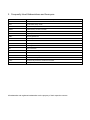
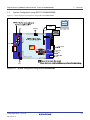
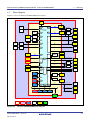
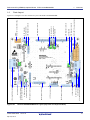
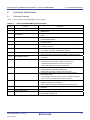
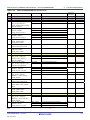
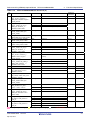
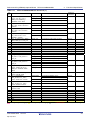
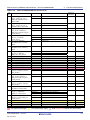
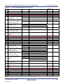
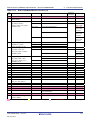
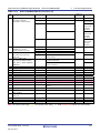
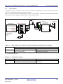
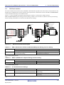
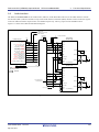
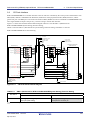
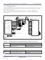
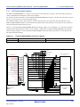
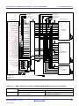
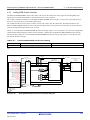
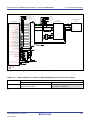
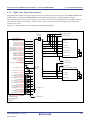
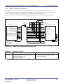
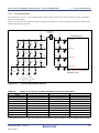
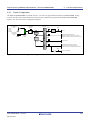
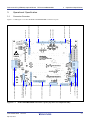
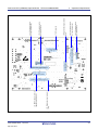
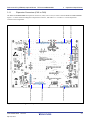
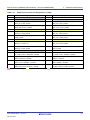
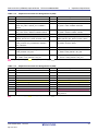
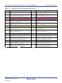
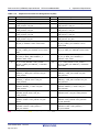
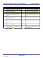
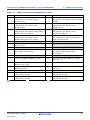
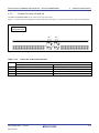
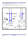
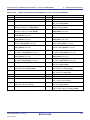
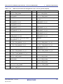
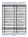
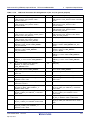
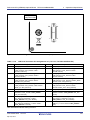
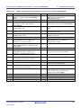
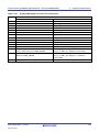
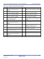
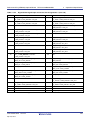
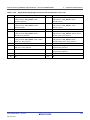
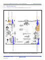
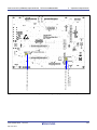
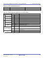
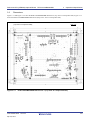
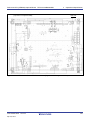
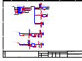
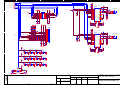
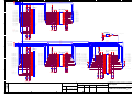
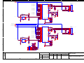
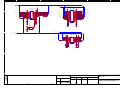
R7S72100 CPU (GENMAI) Optional Board
2.2
RTK7721000B00000BR
2.
Functional Specification
CPU
2.2.1
R7S72100 Overview
The RTK7721000B00000BR is used by connecting with the R7S72100 CPU board RTK772100BC00000BR which has the
32-bit RISK microcomputer with the maximum CPU clock frequency 400MHx.
2.2.2
RTK7721000B00000BR Pin Functions
Table 2.2.1to Table 2.2.14 show the RTK7721000B00000BR Pin Functions.
Table 2.2.1
Pin
No.
RTK7721000B00000BR Pin Functions (1)
Pin Name
A1
Vss
A2
P6_4 / D4 / LCD1_DATA12 /
Function
D4
Description
Expansion
Connector
Data bus
CN1-15
Connected to DIPSW as a clock selection
-
Remarks
CRx2 / IRQ3 / RTS5 / RSPCK1 /
DV0_DATA20
A3
P0_3 / MD_CLKS
MD_CLKS
SW1-5
input.
A4
A5
P11_0 / DV0_DATA12 / TIOC4A /
DV0_DATA12
Connected to DV0 input connector
SCK6 / LCD0_DATA7 / VIO_D12
LCD0_DATA7
Connected to LCD0 output connector
VIO_D12
Connected to CMOS camera input connector
P9_6 / LCD1_DATA22 /
SPBIO20_0
Connected to serial flash memory 1
SPBIO20_0 / SSIWS2 / RTS1 /
LCD1_DATA22
Connected to LCD1 output connector
P9_3 / LCD1_DATA19 /
SPBSSL_0
Connected to serial flash memory 1 and 2
SPBSSL_0 / TxD1
LCD1_DATA19
Connected to LCD1 output connector
P5_9 / WE2/DQMUL / ET_MDC /
ET_MDC
Connected to Ethernet PHY
CN9-28
CN9-24
CS5
A6
A7
CN9-19
CN9-16
DV0_VSYNC / IRQ2 / CRx1 /
IERxD / LCD1_DATA16
JP7:Short
JP7:Open
JP4:2-3
JP7:Open
CRx1
Connected to CAN transceiver
JP4:1-2
IERxD
Connected to IEBus transceiver
JP4:Open
JP2:1-2
JP7:Short
LCD1_DATA16
Connected to LCD1 output connector
JP4:Open
JP2:Open
JP7:Short
A8
Vss
A9
P5_6 / TXOUT0P /
TXOUT0P
Connected to LCD panel for LVDS
-
LCD1_DATA6 / LCD0_DATA22 /
LCD1_DATA6
Connected to LCD1 output connector
CN9-8
DV1_DATA6 / TxD6 / IRQ6 /
DV1_DATA6
Connected to DV1 input connector
SPDIF_IN / DV0_DATA14
A10
P5_2 / TXOUT2P /
TXOUT2P
Connected to LCD panel for LVDS
-
LCD1_DATA2 / LCD0_DATA18 /
LCD1_DATA2
Connected to LCD1 output connector
CN9-4
DV1_DATA2 / SCK3 / TIOC1B /
DV1_DATA2
Connected to DV1 input connector
MOSI3
A11
P5_0 / TXCLKOUTP /
TXCLKOUTP
Connected to LCD panel for LVDS
-
LCD1_DATA0 / LCD0_DATA16 /
LCD1_DATA0
Connected to LCD1 output connector
CN9-2
DV1_DATA0 / TxD4 / TIOC0A /
DV1_DATA0
Connected to DV1 input connector
RSPCK3
A12
Vss
A13
VIN2B
Composite video, blanking, and sync (CVBS)
-
channel 1 input pin2
A14
VDAVss
: 3.3V system power supply,
R20UT2696EJ0005 Rev.0.05
Sep. 06, 2013
: 1.18V system power supply,
: GND, Letters in Red indicate CPU board setting.
2-2