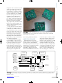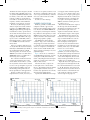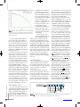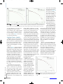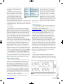
1
Cover - 235.qxp 12/30/2009 11:32 AM Page 1 CIRCUIT CELLAR Various 32-Bit Possibilities, p. 30 • Floating Point for DSP on an FPGA, p. 46 • Forward Error Correction Explained, p. 62 www.circuitcellar.com THEMAGAZINEFOR COMPUTER APPLICATIONS #235 February 2010 WIRELESS COMMUNICATIONS Multi-Functional Wireless Monitoring and Control Build a WWVB-Style Signal Transmitter Customize an Embedded MCU Environment The Advanced Encryption Standard Explained Directional Light Sensor Design $5.95 U.S. ($6.95 Canada) C2.qxp 12/4/2009 2:11 PM Page 1 SSH Encrypted SERIAL TO ETHERNET SOLUTIONS Instantly network-enable any serial device Works out of the box no programming is required Device P/N: SB70LC-100CR Kit P/N: NNDK-SB70LC-KIT $47 Qty. 1000 Customize to suit any application with low-cost development kit SB70LC 256-bit encryption protects data from unauthorized monitoring 2-port serial-to-Ethernet server Features: 10/100 Ethernet TCP/UDP/SSH/SSL modes DHCP/Static IP Support Data rates up to 921.6kbps Web-based configuration Device P/N: SB700-EX-100CR Kit P/N: NNDK-SB700EX-KIT SB700EX 2-port serial-to-Ethernet server with RS-232 & RS-485/422 support $129 Qty. 1000 Need a custom solution? NetBurner Serial to Ethernet Development Kits are available to customize any aspect of operation including web pages, data filtering, or custom network applications. All kits include platform hardware, ANSI C/C++ compiler, TCP/IP stack, web server, email protocols, RTOS, flash file system, Eclipse IDE, debugger, cables and power supply. The NetBurner Security Suite option includes SSH v1 & v2 support. Device P/N: CB34-EX-100IR Kit P/N: NNDK-CB34EX-KIT $149 Qty. 1000 CB34EX industrial temperature grade 2-port serial-to-Ethernet server with RS-232 & RS-485/422 support and terminal block connector Information and Sales | [email protected] Web | www.netburner.com Telephone | 1-800-695-6828 9.qxp 8/7/2008 11:04 AM Page 1 2-3.qxp 11/2/2009 3:52 PM Page 2 2-3.qxp 11/2/2009 3:52 PM Page 3 Task_Masthead_235.qxp 1/13/2010 11:58 AM Page 4 T ASK MANAGER Choose Your Own Design Adventure February 2010 – Issue 235 W 4 hen I was a child, I read a few of the books in Bantam’s “Choose Your Own Adventure” series. The point was to make decisions that would influence the course of the tale. Decisions were presented in a simple format. Example: To do X, turn to page 5. To do Y, turn to page 10. As a book’s main character, I’d drive the story by turning to certain pages and then reading on. Some choices led to situations in which the main character was rewarded. Other choices led to negative scenarios, such as the main character’s death. Thus, each book had a few possible endings. Hmm. That’s kind of like each issue of Circuit Cellar (except for the death part). Let’s say that while reading a project-centric article you become so interested in a part that you immediately go to the manufacturer’s website. That’s one adventure. Now imagine that instead of checking out the part you decide to get more information by emailing the author. That’s another adventure. The great thing about Circuit Cellar is that each issue provides the possibility for dozens of engineering adventures. You’re in charge. I urge you to approach this issue in the spirit of choosing your own adventure. Are you ready? Let’s begin. Turn to page 16 to learn how to build an RFID-based monitoring and control system. Brian Millier describes how he designed a wireless control system for a liquid nitrogen tank. To learn how to start an FPGA-based embedded design, jump to John Clayton’s article on page 24. He covers topics ranging from custom development environments to HDL coding/synthesis tools. For more FPGA-related content, check out Bruce Land’s article on page 46. Skip to page 30 to learn why Tom Cantrell says many MCU suppliers are “betting” on the ARM Cortex-M3. Are you with them? On page 38, Ed Nisley presents a “totally featureless clock” design, which requires you to first build a WWVB simulator. Are you fascinated in the Advanced Encryption Standard (AES) but put off in the complicated math? You aren’t alone. Go to page 54 for Monte Dalrymple’s useful presentation of the AES. If you’re confused by the topic of forward error correction (FEC), refer to Robert Lacoste’s article on the subject (p. 62). It’s a great introduction to the subject. Jeff Bachiochi wraps up the articles section of the issue with the first installment of his “Sun Tracker” article series (p. 68). This project enables you to tell time with a mixture of old and new technologies. Sundials, sensors, and MCUs. Now that’s a bill of materials bound to lead to an amazing design adventure. As usual, we have a lot of handy information packed in a single issue. You can’t build all the projects and test all the theories at once, so choose your adventure wisely. There’s no rush. You can always return to the issue to start a new journey. [email protected] CIRCUIT CELLAR ® THE MAGAZINE FOR COMPUTER APPLICATIONS FOUNDER/EDITORIAL DIRECTOR Steve Ciarcia PUBLISHER Hugo Vanhaecke MANAGING EDITOR C. J. Abate MARKETING Shannon Barraclough WEST COAST EDITOR Tom Cantrell CUSTOMER SERVICE Debbie Lavoie CONTRIBUTING EDITORS Jeff Bachiochi Robert Lacoste George Martin Ed Nisley CONTROLLER Jeff Yanco ART DIRECTOR KC Prescott GRAPHIC DESIGNERS Grace Chen Carey Penney NEW PRODUCTS EDITOR John Gorsky PROJECT EDITORS Gary Bodley Ken Davidson David Tweed STAFF ENGINEER John Gorsky ADVERTISING 800.454.3741 • 978.281.7708 • www.circuitcellar.com/advertise ADVERTISING REPRESENTATIVE Peter Wostrel Strategic Media Marketing, Inc. 1187 Washington St., Gloucester, MA 01930 USA 800.454.3741 • 978.281.7708 [email protected] • www.smmarketing.us Fax: 978.281.7706 ADVERTISING COORDINATOR Valerie Luster E-mail: [email protected] Cover photography by Chris Rakoczy—Rakoczy Photography www.rakoczyphoto.com PRINTED IN THE UNITED STATES CONTACTS SUBSCRIPTIONS Information: www.circuitcellar.com/subscribe, E-mail: [email protected] Subscribe: 800.269.6301, www.circuitcellar.com/subscribe, Circuit Cellar Subscriptions, P.O. Box 5650, Hanover, NH 03755-5650 Address Changes/Problems: E-mail: [email protected] GENERAL INFORMATION 860.875.2199, Fax: 860.871.0411, E-mail: [email protected] Editorial Office: Editor, Circuit Cellar, 4 Park St., Vernon, CT 06066, E-mail: [email protected] New Products: New Products, Circuit Cellar, 4 Park St., Vernon, CT 06066, E-mail: [email protected] AUTHORIZED REPRINTS INFORMATION 860.875.2199, E-mail: [email protected] AUTHORS Authors’ e-mail addresses (when available) are included at the end of each article. CIRCUIT CELLAR®, THE MAGAZINE FOR COMPUTER APPLICATIONS (ISSN 1528-0608) is published monthly by Circuit Cellar Incorporated, 4 Park Street, Vernon, CT 06066. Periodical rates paid at Vernon, CT and additional offices. One-year (12 issues) subscription rate USA and possessions $29.95, Canada/Mexico $34.95, all other countries $49.95.Two-year (24 issues) subscription rate USA and possessions $49.95, Canada/Mexico $59.95, all other countries $85. All subscription orders payable in U.S. funds only via Visa, MasterCard, international postal money order, or check drawn on U.S. bank. Direct subscription orders and subscription-related questions to Circuit Cellar Subscriptions, P.O. Box 5650, Hanover, NH 03755-5650 or call 800.269.6301. Postmaster: Send address changes to Circuit Cellar, Circulation Dept., P.O. Box 5650, Hanover, NH 03755-5650. Circuit Cellar® makes no warranties and assumes no responsibility or liability of any kind for errors in these programs or schematics or for the consequences of any such errors. Furthermore, because of possible variation in the quality and condition of materials and workmanship of reader-assembled projects, Circuit Cellar® disclaims any responsibility for the safe and proper function of reader-assembled projects based upon or from plans, descriptions, or information published by Circuit Cellar®. The information provided by Circuit Cellar® is for educational purposes. Circuit Cellar® makes no claims or warrants that readers have a right to build things based upon these ideas under patent or other relevant intellectual property law in their jurisdiction, or that readers have a right to construct or operate any of the devices described herein under the relevant patent or other intellectual property law of the reader’s jurisdiction. The reader assumes any risk of infringement liability for constructing or operating such devices. Entire contents copyright © 2010 by Circuit Cellar, Incorporated. All rights reserved. Circuit Cellar is a registered trademark of Circuit Cellar, Inc. Reproduction of this publication in whole or in part without written consent from Circuit Cellar Inc. is prohibited. CIRCUIT CELLAR® • www.circuitcellar.com 5.qxp 1/11/2010 9:11 AM Page 1 INSIDE ISSUE 235 February 2010 • BONUS CONTENT Using USB for Computer Interfacing Projects Wireless Communications 16 24 p. 16, RFID Tech p. 24, Designing with an FPGA 46 54 RFID-Based Liquid Control (Part 1) Working with Off-the-Shelf Components Brian Millier FPGA Embedded Microcontroller Environment John Clayton Floating Point for DSP Bruce Land Advanced Encryption Standard Understanding AES Without Math Monte Dalrymple p. 38, Featureless Clock Design 30 38 February 2010 – Issue 235 62 6 68 SILICON UPDATE A Winning Hand Betting on the ARM Cortex-M3 Tom Cantrell ABOVE THE GROUND PLANE Totally Featureless Clock (Part 1) WWVB Simulator Ed Nisley THE DARKER SIDE Living with Errors An Introduction to Forward Error Correction Robert Lacoste FROM THE BENCH Sun Tracker (Part 1) Create a Directional Light Sensor Jeff Bachiochi TASK MANAGER Choose Your Own Design Adventure C. J. Abate 4 NEW PRODUCT NEWS edited by John Gorsky 8 CROSSWORD 74 INDEX OF ADVERTISERS 236 Preview 79 PRIORITY INTERRUPT Feature Creep Steve Ciarcia 80 CIRCUIT CELLAR® • www.circuitcellar.com 29.qxp 11/30/2009 12:49 PM Page 1 The New High-Performance Catalog Industry’s only full-featured online catalog •Browse •Search •Check Stock tock k •Buyy Try It Now at www.mouser.com WARNING: Designing with Hot, New Products May Cause A Time-to-Market Advantage. Introducing the new, enhanced, high-tech online catalog. Allowing you to browse, search, check stock, buy, and more — An industry rst And only online catalog to offer all these features without ever having to leave the catalog!. www.mouser.com (800) 346-6873 Mouser and Mouser Electronics are registered trademarks of Mouser Electronics, Inc. Other products, logos, and company names mentioned herein, may be trademarks of their respective owners. Mouser_CircuitCellar_Jan.indd 1 11/24/09 1:40:11 PM npn235.qxp 1/8/2010 1:09 PM Page 8 WIRELESS SENSOR NETWORK DEVELOPMENT TOOLSET The @ANY DESIGN development kit is a new toolset for the development of 868/915-MHz wireless sensor network applications in energy management, smart metering, industrial and building automation, and more. The easy-to-use toolset includes @ANY900 RF modules, USB dongles, development tools, and embedded software, supporting IEEE 802.15.4based protocols, including ZigBee PRO and 6LoWPAN, as well as proprietary solutions. Combined with Adaptive Network Solutions’s RF design and customization services, these tools empower OEMs and system integrators to take their new products from concept to market faster and more cost-effectively. The development kit provides developers with everything they need to create market-ready wireless systems and applications, while mastering the intricacies of WSN technology. The kit features support of third-party applications and convenient reference drivers, as well as APIs for UART, I2C, ADC, and 1-wire peripherals. The @ANY DESIGN kit supports the intuitive development environment from Atmel, including an embedded debugging feature using Atmel JTAG in-circuit debugger. The @ANY DESIGN development kit consists of an @ANY900 USB dongle with JTAG programming adapter, three fully programmable @ANY BRICK boards, and a CD-ROM containing documentation and software, including the Smart MAC Suite software toolchain and network visualization tool. The development kit can be extended with additional @ANY900 BRICK development boards and @ANY900 USB dongles on an as-needed basis. @ANY DESIGN development kits (Part number @ANY 900 DK) cost approximately $440. Adaptive Network Solutions GmbH www.an-solutions.de COMPACT ANTENNAS WITH SMA CONNECT OR Antenna Factor’s HW Series half-wave center-fed dipole antennas and quarter-wave monopole antennas are now available with standard SMA connector terminations. HW Series antennas are ideal for applications requiring a com- pact, low-cost antenna solution. These antennas attach using an FCCcompliant RP-SMA connector or the newly available standard SMA connector. Alternate connectors and custom colors are available for volume OEM orders. The antennas are available in standard center frequencies of 315, 418, 433, 868, and 916 MHz. The 868 and 916 MHz versions are half-wave center-fed dipoles, while the 315, 418, and 433 MHz versions are all quarter-wave monopoles. The HW Series feature an internal counterpoise, an omnidirectional pattern, outstanding VSWR, and excellent performance. The antennas are rugged and damage-resistant. HW Series antennas cost $4.98 in volume quantities. February 2010 – Issue 235 Antenna Factor www.antennafactor.com 8 E WS N CT DU R O P EW N Edited by CIRCUIT CELLAR® • John Gorsky www.circuitcellar.com npn235.qxp 1/8/2010 1:09 PM Page 9 ULTRA LOW-POWER, LOW-PROFILE COOLER USES PULSES OF AIR The new NtelliJet series of low-profile, low-acoustic coolers uses rapid-fire pulses of turbulent air (produced by an oscillating diaphragm working between 50 and 200 Hz ) to cool heatsinks and surrounding components. The features of the NtelliJet cooler present an entirely new concept of thermal cooling ability. In addition to ultra-high reliability and low-profile height (max. 15 mm), there is also a total elimination of mechanical wear, dirt, and dust clogging. The new series is also immune to shock and vibration, and it provides an impressive 100,000 hours of life at 60°C. The NtellJet is ideal for focused thermal requirements, when cooling is needed for specific chips or areas of coverage. The NtelliJet offers a flexible alternative for fans across a large range of industrial applications and designs. Designed for directed cooling, the NtelliJet optimizes heat exchange through the use of turbulent, high-velocity jets. The vortex-dominated flow enhances small-scale mixing near the heated surfaces to yield higher effective heat transfer at low-volume flow rates compared to conventional air movers. The NtelliJet flow is created using patented actuator technology and proprietary fluidic packaging expertise. The system-wide heat removal takes advantage of the ejector effect inherent to high-momentum jet flows. As it operates, the NtelliJet module expels high momentum pulses of air. Each pulse of air “entrains” or pulls nearby ambient air behind it in its wake. Please contact JARO Thermal directly for pricing information. JARO Thermal www.jarothermal.com February 2010 – Issue 235 NPN S www.circuitcellar.com • CIRCUIT CELLAR® 9 npn235.qxp 1/8/2010 1:09 PM Page 10 HIGH-PERFORMANCE 125-KHZ LF WAKEUP RECEIVER The AS3930 is a single-channel, low-power, low-frequency wakeup receiver that offers the highest sensitivity at the lowest current consumption for the industry’s best range. The AS3930 supports the widely used 125-kHz band and—through the optimization of power consumption, sensitivity and programmability—enables a variety of applications. The AS3930 has a single receiving channel and an internal RC oscillator, allowing a very low external component count for maximum performance versus cost and reduced size. The received data can be correlated with a pattern that is programmed in the register preventing false wakeups. Primary target applications are active RFID, high-value asset tracking, real-time location systems, operator identification and access control or keyless entry. The AS3930 wakeup receiver is available in a TSSOP16 or a QFN (4 × 4) package. It is suitable for operating environments ranging from –40° to 85°C. The AS3930 is priced at $2.30 each in 1,000-unit quantities. austriamicrosystems AG www.austriamicrosystems.com ETHERNET DATA RADIO The SureCross DXER9 Ethernet data radio is an industrial-grade, long-range, 900-MHz radio used to create point-to-multipoint configurations of wireless Ethernet networks. The DXER9 is designed for industrial applications and will perform reliably in applications that prove too noisy or too far for standard Wi-Fi-based systems. This is a high-gain system that has over 10 times the range of a Wi-Fi network. It offers an outside line of sight range of 10-plus miles and an indoor range of 1,500-plus feet (easily penetrating walls). Key features include 128-bit AES encryption, sub-block error detection and retransmission, and automatic scan or manual override for the best of 12 communication channels. It also features indicator LEDs for channel selection and signal strength, point-to-multipoint configurations with up to 16 subscriber units, and up to 12 access points per site to provide a total of 192 points. User configuration is via an internal web-page. Please contact Banner Engineering for pricing. Banner Engineering www.bannerengineering.com February 2010 – Issue 235 DIGITAL PREAMPLIFIER CONTROLLER IC 10 The THAT5171 is a new digital gain controller IC for lownoise analog, differential, current-feedback audio preamplifiers. When used in conjunction with an appropriate analog gain block, the 5171 can set gain in 1-dB steps while preserving low noise and distortion. The 5171 operates from ±5 V to ±17 V supplies and supports input signal levels as high as 22 dBu at 5.6 dB gain and ±17 V supplies, with gain error guaranteed at +/- 0.5 dB, maximum, at all gain settings. Applications for the 5171 include digitally controlled instrumentation amplifiers, digitally controlled differential amplifiers, and a variety of digitally controlled audio instrumentation. The 5171 mates with the THAT1570 differential audio preamplifier IC for a best-in-class solution for digitally con- trolled audio preamplifiers. For designers who prefer a more customized solution, the 5171 may be used to control a discrete preamplifier. To reduce “zipper noise” in audio applications, the 5171 includes a differential servo and zerocrossing detector to minimize DC offsets and glitches during gain adjustments. The 5171 is controlled via an addressable SPI port. Four general-purpose digital outputs can be controlled via this interface. The SPI bus supports read-back so that host software can verify proper operation. The THAT5171 comes in a 7 mm × 7 mm QFN32 package. It costs $6.70 in 1,000-piece quantities. THAT Corp. www.thatcorp.com NPN CIRCUIT CELLAR® • www.circuitcellar.com npn235.qxp 1/8/2010 1:09 PM Page 11 ADVANCED FAMILY OF ZIGBEE MODULES The ETRX3 series is a third generation of advanced ZigBee module and the first module family on the market to feature the EM357 and EM351—the latest ARM Cortex M-3 SoCs from Ember. ETRX3 series modules have a footprint of just 19 mm × 25 mm for both standard and PA/LNA versions, which represents a 40% reduction in size compared to the ETRX2 module. They are available with either an on-board antenna or a Hirose U.FL connector for an external antenna. A link budget of 105 dB on the standard ETRX3 module gives excellent performance, and RF power can be further boosted by the ETRX3-LR, which adds an extra LNA+PA boosting the link budget to 123 dB. The ETRX3 series modules integrate a 2.4-GHz, IEEE 802.15.4-compliant transceiver with up to 192 KB of flash memory, 12 KB of RAM, and many advanced peripherals. To maintain the strict timing requirements imposed by the ZigBee and IEEE 802.15.42003 standards, the EM357and EM351 integrate a number of MAC functions into the hardware, handling automatic ACK transmission and reception, automatic back-off delay, clear channel assessment for transmission, and the automatic filtering of received packets. ETRX3 series modules work from a 2.1- to 3.6-V supply and active power consumption is reduced by over 20% compared to the ETRX2. In deep sleep mode, current consumption is reduced to 800 nA and further reduced to 400 nA if the self wakeup feature is not enabled. The ETRX3 series is available from Lemos International (Telegesis’s U.S. distributor). Pricing starts at $18 in small quantities. Lemos International Corp. www.lemosint.com February 2010 – Issue 235 NPN www.circuitcellar.com • CIRCUIT CELLAR® 11 npn235.qxp 1/8/2010 1:09 PM Page 12 LOW-COST WIRED AND WIRELESS NETW ORKING MODULES Rabbit has expanded its MiniCore series of easy-to-use, ultra-compact, low-profile, low-cost networking modules. Available in pin-compatible wired and Wi-Fi versions, the family now includes the Ethernet RCM5760 and Wi-Fi RCM5650W. The new modules offer increased memory for data-intensive applications, such as building automation and security applications. The products also allow a customer to wirelessly update firmware from anywhere an Internet connection is available to reduce maintenance costs. The MiniCore family provides a rich embedded feature set on an ultra-compact mini PCI Express form factor. Its small size makes it easy for customers to place wired or wireless network connectivity anywhere on a motherboard. The family includes the pin-compatible and interchangeable wired RCM5700, Wi-Fi RCM5600W, wired RCM5760, and Wi-Fi RCM5650W. Rabbit MiniCore products feature 10/100 Base-T Ethernet and secure 802.11 b/g with WPA2 and 802.11i compliance for the highest levels of security. It also features up to 640-KB SRAM data storage, 1-MB flash memory for program storage and two MB serial flash for mass storage. Depending on the version, modules include up to 32 GPIO, six serial ports, a serial-to-Ethernet bridge, an embedded Web server for greater application control monitoring and wireless remote firmware update functionality. The Ethernet RCM5700 kit costs $99. The Wi-Fi RCM5600W kit, with one year of free tech support, is available now for a promotional price of $149. Rabbit, Inc. www.rabbit.com February 2010 – Issue 235 NPN 12 CIRCUIT CELLAR® • www.circuitcellar.com npn235.qxp 1/8/2010 1:09 PM Page 13 HIGH-PERFORMANCE, SMALL-FOOTPRINT DEVELOPMENT BOARD The Chameleon is the next step in the evolution of the high-performance, small-footprint, application development board. It is a credit cardsized computer with two processors, nine processing cores, 1 MB of onboard flash memory, and 64 KB of EEPROM. It also includes numerous I/O interfaces that include composite video for NTSC/PAL, VGA, audio out, PS/2 for keyboards and mice. Additionally, it has a number of digital I/Os and analog inputs. The power of the Chameleon is in its dual-processor design. It is available in two flavors—an AVR 8-bit version and a PIC 16-bit version. The AVR version uses the Atmel AVR328P processor, while the PIC version uses the Microchip Technology PIC24 as the main master processor (client) along with the multicore Propeller chip as the media processor (server). The AVR/PIC sends commands to the Propeller chip over a high-speed SPI to command the Propeller to execute various operations all with a simple API that usually consists of a few lines of code to perform any task. Thus, the AVR/PIC programming is easy; and with simple APIs, engineers can develop complex and rich media applications. Both versions are designed to have Arduino I/O header compatibility as much as possible, but the AVR version is additionally 100% software-compatible and the Arduino tool can be used to develop software for the AVR version (as well as AVRStudio). The PIC version works with MPLab as well as a standalone “Arduino-like” tool chain that relies on a bootloader. A complete BASIC programming language for the Chameleon is available. Code can be written on a PC with a simple editor, compiled, and downloaded to the Chameleon. The Chameleon also features a “break away” experimentation protoboard built into the PCB. The Chameleon costs $59.95 for the AVR version and $69.95 for the PIC version. Nurve Networks LLC www.xgamestation.com February 2010 – Issue 235 NPN www.circuitcellar.com • CIRCUIT CELLAR® 13 npn235.qxp 1/8/2010 1:10 PM Page 14 DEVELOPMENT ENVIRONMENT IN A SPORTS WATCH Representing a new era in development, Texas Instruments has announced the eZ430-Chronos, the world’s first customizable development environment within a sports watch. Taking the popular line of eZ430 development tools to the next level, the kit allows developers to easily harness the capabilities of the CC430 microcontroller. The Chronos is designed to provide customers with all of the hardware and software needed to immediately begin development of wireless networking applications, regardless of programming expertise. The kit is equipped with sensors for measurement and motion-based control and can serve as a central hub for nearby wireless sensors so that users have remote access to real-time data from devices such as pedometers and heart rate monitors. Sensors in the kit include an integrated threeaxis accelerometer, an altimeter, along with temperature and battery voltage sensors. Also included is a large 96-segment LCD. The Chronos includes a USB-RF access point for wireless set-up and PC connectivity, as well as multiple production-ready open-source projects to foster easy evaluation, design, and community collaboration. The kit is available in three different RF frequency bands—915, 868, and 433 MHz—allowing for worldwide usage. TI’s SimpliciTI and BM Innovations’s BlueRobin RF protocols enable developers to easily establish wireless links (regardless of their RF knowledge) right out of the box. The new eZ430-Chronos costs $49. Texas Instruments, Inc. www.ti.com February 2010 – Issue 235 ProtoMat® Benchtop PCB Prototyping Machine 14 What would your day look like tomorrow if you could cut yourself free from the board house and produce true, industrial quality PCBs right at your desk? LPKF’s ProtoMat benchtop prototyping systems are helping thousands of engineers around the world take their development time from days and weeks to minutes and hours. In today’s race to market, it’s like having a time machine. www.lpkfusa.com/pcb 1-800-345-LPKF “You can’t beat an LPKF system for prototyping. We do up to three iterations of a design within a day.” Leonard Weber Agilent NPN CIRCUIT CELLAR® • www.circuitcellar.com How far will your design take you? Challenge yourself against other top embedded engineers around the world in DesignStellaris 2010, sponsored by Texas Instruments. Use the Stellaris® LM3S9B96 microcontroller from Texas Instruments with Keil’s RealView® Microcontroller Development Kit (RVMDK) and SafeRTOS™ from Wittenstein to create your design content entry, and see how far your design will take you! Stellaris EKK-LM3S9B96 Evaluation Kit free with your contest entry while supplies last! • No purchase necessary to enter. • $10,000 in cash prizes! The EKK-LM3S9B96 Evaluation Kit includes: an evaluation board with an 80 MHz LM3S9B96 MCU featuring Ethernet MAC+PHY, CAN, USB OTG, and SafeRTOS in ROM; a time-limited copy of the Keil RealView Microcontroller Development Kit, cables, documentation, and StellarisWare® software. • Entry deadline is June 23, 2010. • Winners will be announced at the Embedded Systems Conference Boston 2010. • Submit your design today! For Complete Details, Visit: www.ti.com/designstellaris2010 1/11/2010 9:15 AM Page 16 F EATURE 2102014_millier.qxp ARTICLE by Brian Millier RFID-Based Liquid Control (Part 1) Working with Off-the-Shelf Components With this article series, you’ll learn how to build an RFID-based controller for monitoring dispensed liquid nitrogen from a tank. Operated in a laboratory setting, the system also bills customers for what they use. This article details how to get started with some off-the-shelf components and simple code. February 2010 – Issue 235 T 16 to transfer the transactions stored in the controller to a USB he recent commercialization of electronic devices like flash drive as standard files. These files are readily imported radio frequency identification (RFID) tags and USB flash into an Excel spreadsheet on a computer in our accounting drives has made it possible to design such things as vending office. An alternate scheme would be to link the dispensing kiosks and building access controls, which are both affordable controller to a computer in the accounting office via an Etherand user-friendly. Furthermore, the availability of inexpensive net connection. But running a dedicated 10BaseT connection modules—which encapsulate the often complex protocols and operating the controller as an Internet node would cost used by such devices—is a boon to designers who don’t have the expertise to augment their product’s firmware. I built a controller that monitors the liquid nitrogen disb) pensed from a tank and bills customers for what they use (see Photo 1). The tank is located in the basement of my building at Dalhousie University in Halifax, Canada. RFID tags costing less than $1 are issued to each customer. The controller has a low-cost RFID reader module. After passing the tag near the controller, the customer interacts with an LCD and keypad to enter the amount of liquid needed. The cona) troller maintains a realtime clock (RTC) circuit, and it stores the account number, sales data, and a time/date stamp for each transaction. All transaction records are maintained internally using E2PROM. A USB host port on Phhoto oto 1a—This 1a —This is the dispenser. The VDrive2 module, which the USB flash drive plugs into, is tucked away the controller is the — Almost all of the ciron the left side panel because it is not accessed by the liquid nitrogen customers. bb—Almost aspect of the design cuitry is mounted behind the front panel (on the bottom). The main power supply components are mounted that makes it so userin the enclosure’s body. The VDrive2 module is visible above the main circuit board. The solenoid valve is on the right. friendly. It enables me CIRCUIT CELLAR® • www.circuitcellar.com 1/13/2010 10:49 AM 1 4 4 × 20 LCD 2 5 Page 17 3 A 6 B 7 8 9 C * 0 # D 3-V Coin cell DS1307 RTC 74C922 1,024-KB I2C EEPROM (×2) LF RFID Reader 2:1 Mux RFID Tag 4052 Serial in/out ATmega32 VDrive 2 Dev. select USB Flash drive Solenoid valve Figure 1— The project is built around an ATmega32. You can see how the RFID reader and the VDrive2 module interact. more than using a USB flash drive. In this article, I’ll describe how I simplified the design by using an offthe-shelf RFID reader module and a Vinculum VDrive2 module, which handles reading and writing files to a USB flash drive. All told, the project consists of an Atmel ATmega32 microcontroller and just five other peripheral chips (see Figure 1). I wrote the code in BASCOM BASIC. AFFORDABLE LAB SOLUTION In the past, I’d considered Smart Cards for this application (B. Millier, “BasicCards 101,” Circuit Cellar 164). But when I came to this project, I concluded that an ideal solution would include RFID tags for user validation and a USB flash drive (64 MB suffices) for file transfers. Cost is probably the biggest project limitation in the Department of Chemistry where I work. Therefore, the first thing I looked into was the cost of the RFID devices and an associated reader. The cost of readers varies widely, and it becomes significant if you are just setting up a small system. Fortunately, I www.circuitcellar.com • CIRCUIT CELLAR® found a low-cost reader that would work with inexpensive RFID tags, so I had a good start to my design. I then investigated the best way to incorporate a USB flash drive into my design. I settled on a product from FTDI, which produces various USB modules, some of which I had used in earlier projects. I consider the Vinculum VDrive2 module to be a USB flash drive coprocessor. It interfaces to a microcontroller via a serial port and handles all the complexity of the drive’s FAT32 file system. Thirty years ago, when I was building my own PC from boards and components, I wrote my own simple floppy disk operating system in assembly code. Today, however, I’d rather leave that chore to the programmers at FTDI. DESIGN OVERVIEW Before examining the details of the various modules used in the project, refer back to Figure 1. The RFID reader is a low-cost module that signals the presence of a low-frequency RFID tag by sending the tag’s unique, 10-hex-character ID code via a 9,600-bps RS-232 link. Upon authentication, you interact with the controller via a 4 × 20 LCD and a numeric keypad. The transaction data and RFID identification code memory is provided by two Microchip Technology 24AA1025 1,024-Kb I2C flash memory devices, yielding a total storage capacity of 256 KB of nonvolatile memory. The controller opens a solenoid valve for an interval timed to dispense the desired volume of liquid nitrogen. An RTC circuit is needed because the time and date of each transaction must be stored with its record. The ATmega series of microcontrollers does not include a dedicated RTC module featuring a separate battery back-up power supply pin. Therefore, I chose the common Maxim Integrated Products DS1307 I2C RTC chip with a 3-V coin cell for back-up power. Transferring the data from the transaction tables stored in the controller’s I2C flash memory over to a remotely located PC is accomplished with a USB flash drive. The flash drive is interfaced to the microcontroller via the Vinculum VDrive2 module. This module communicates via a full-duplex serial data link. All the firmware needed to work with the USB flash drive’s FAT32 file structure is handled by the VDrive2. It does so in response to ASCII commands sent to it via its serial link. Because the RFID reader and the VDrive2 modules are never used simultaneously, it’s possible to multiplex both modules to the single serial port present on the ATmega32 microcontroller using an ON Semiconductor MC14052 multiplexer chip. You might wonder why I didn’t use the USB flash drive to handle the controller’s nonvolatile storage needs. Why bother with the two 24AA1025 1,024-KB I2C flash memory devices at all? The main reason is that I wanted a userfriendly design. I wanted to be able to merely plug a USB flash drive into the externally mounted VDrive2 module (once a month) to download the transaction figures. If the USB flash drive were to be used to store all the transaction data (as it was being collected), the drive would have to be connected all the time. That would involve mounting it inside the controller’s cabinet, behind a locked access door; otherwise, someone could just steal it. While the current cost of a 64-MB February 2010 – Issue 235 2102014_millier.qxp 17 40-41.qxp 8/5/2009 9:53 AM Page 40 40-41.qxp 8/5/2009 9:53 AM Page 41 2102014_millier.qxp 1/11/2010 9:15 AM flash drive is practically negligible, the transaction data is not! Mounting two small I2C flash memory devices on the controller board was more practical than worrying about a cabinet with a locked access door. It also helped that Microchip had sent me some free samples of the 24AA1025 flash devices. RFID TAGS & READERS February 2010 – Issue 235 RFID tags come in various packages, sizes, and prices. Some readers can cost thousands of dollars depending on their 20 Page 20 intended uses. My cost constraints meant that I had to find tags or cards worth less than a $1, as well as a comparably low-cost reader. In an RFID scheme, the reader generally consists of a pulsed transmitter/ receiver. The reader’s transmitter produces enough RF energy at a specific frequency. Thus, when a matching RFID tag comes into proximity, the tag’s antenna extracts enough energy from this RF field to charge a small capacitor inside it. The stored energy is then used to power a small microcontroller in the tag which either sends back a short burst of RF energy or modulates the reader’s own transmitted signal by “shorting out” its own antenna. In either case, the modulated RF field is encoded with a pattern that’s unique to that particular tag. The reader decodes this ID information and sends it as a message to an external microcontroller, usually via a serial data link. The most common RFID tags—the socalled low-frequency (LF) tags—operate at 125 kHz. ISO14443 high-frequency (HF) cards operate at 13.56 MHz. All things being equal, the HF tags would require a much smaller antenna, which is advantageous if one needs physically smaller tags. Also, due to the higher carrier frequency, the HF tags can transmit much more information in a given amount of time, which is beneficial in some applications. Therefore, LF tags are often used when all that is needed is a unique ID code per tag—frequently a unique 10character (hex) code. The HF tags can be used when you need the ability to store a larger amount of data in the tag. With HF tags, the reader is often also able to write data to the tag as part of the transaction that occurs when the tag is near it. All that I needed for this project was a tag with a unique ID code, nothing more. Furthermore, because the tag wasn’t going to be embedded inside a product or worn, it would be easy for the user to bring it up close to the reader, removing the need for a long-range system. While searching the Internet, I found a reasonably priced tag/reader LF system distributed by Futurlec. The company’s EM LF RFID reader module costs only $33, and it also carries a variety of tags: plastic “credit cards,” key fobs, dog collar tags, laundry tags, and so on. For my purposes, 30-cm plastic keychain tags seemed the best choice. They were only $0.80 each, even in multi-unit quantities. I chose the EM card reader because it’s easy to use and interface. Physically, it’s built to be mounted like a conventional wall lighting switch (i.e., it can be mounted to the standard electrical box used for lighting switches). CIRCUIT CELLAR® • www.circuitcellar.com 21.qxp 12/30/2009 10:19 AM Page 1 MobileLife } Mobile Business 2102014_millier.qxp 1/13/2010 10:45 AM Page 22 A 12″ eight-conductor cable exits from the back of the unit. All you need to do is supply the unit with 9 to 12 VDC, and monitor the 9,600-bps, RS-232 level signal on the TxD wire. The reader’s front panel contains a two-color LED that illuminates red when the unit is powered up and flashes green when a valid RFID tag is nearby. The unit also has a loud piezo buzzer that beeps when a matching RFID tag is sensed. These built-in user feedback features are handy because you don’t have to write DISCOVER . C ONN code or use any I/O port lines for them. There are also control wires to externally control the buzzer and the LED, but I didn’t use them. Whenever a valid RFID tag is near, the reader sends a message via its TxD wire in the following format: STX, ID1,ID2,ID3,ID4,ID5,ID6,ID7,ID8, ID9,ID10,ETX Note that STX is ASCII code 02H. ETX is ASCII code 03 H. IDx is 10 ASCII TH . T EC V RI E. VINCULUM VDRIVE2 Opportunities New Suppliers Equipment Demonstrations Solutions Network Industry Experts Emerging Technologies Solutions February 2010 – Issue 235 DESIGN 22 U OARD PRINTED B CONFERENCE & EXHIBITION April 6–8, 2010 MEETINGS & EDUCATION April 6–9, 2010 Mandalay Bay Resort & Convention Center Las Vegas, Nevada www.IPCAPEXEXPO.org S U TEST U ELE CT N RO IC characters representing hex values. Although the datasheet is sparse and not translated well into English, it appears that ID1 through ID8 form a 64-bit code, and ID9 and ID10 are the checksum of the previous 8 bytes. However, the datasheet also mentions XOR, which is used for CRC error-checking, not checksum error calculations. In any case, I considered all 10 characters as the ID code. I bought my reader several months ago. Futurlec now carries a slightly different model. It costs about the same and mounts in the same fashion, but it has fewer interface wires and is black rather than white. But I suspect that it operates identically. S S A M SE Y BL THERE’S NO OTHER SHOW LIKE IT IN THE WORLD! Benefit from the industry’s premier technical conference, half-day courses, Designers Day and IPC standards meetings. Solve your manufacturing challenges, visit hundreds of exhibitors and meet thousands of peers and industry experts in electronics manufacturing. Focus on critical areas, such as high speed signal integrity PCB design, materials compliance, design for manufacture and embedded technologies. Pre-register for free exhibit hall admission and take advantage of free keynotes, posters, forums and networking events. FTDI spun off a subset of its USB devices into what it calls the Vinculum line. Vinculum is Latin for a bond or a tie, and that is what these devices do: they tie USB devices together. You are probably familiar with the various USB serial and USB parallel chips/modules which the company also makes. You’ll find them embedded in many commercial products, including many microcontroller evaluation boards and device programmers, for example. The USB serial and parallel chips/modules are USB slaves—that is, they’re meant to be plugged into a USB host controller, which is in most cases a computer of some sort. The main purpose of the USB serial device is to enable a manufacturer to modernize a design that includes an RS-232 data link into one that communicates via USB. Many newer computers no longer contain serial ports, but have numerous USB ports. The Vinculum line is different in that it implements a USB host controller (as well as other functions). Thus, if you are using a microcontroller, you can easily connect a great variety of low-cost, consumer devices (e.g., such as flash drives and HID class devices) without having to worry about adding the USB host controller protocol to your firmware. The Vinculum line starts out with the VNC1L USB host controller chip. This contains two USB 2.0 ports, which can be configured in either Host or Slave mode. This enables you to connect a USB flash drive to your microcontroller-based CIRCUIT CELLAR® • www.circuitcellar.com 2102014_millier.qxp 1/11/2010 9:16 AM Page 23 design. It also allows you to connect your device to a PC to upload or download data or program information. The VNC1L chip is really a fullfledged system on a chip because it contains an MCU core, 64 KB of flash memory, 4 KB of SRAM, dual DMA controllers, a UART, a SPI and a PS2 port, and a lot of general-purpose I/O. The chip is delivered unprogrammed, but FTDI offers several versions of firmware, which you can download to the device’s flash memory via its UART port and the bootloader firmware built into the device. FTDI provides a PC application called VPROG that enables you to program (and reprogram) the firmware into the VNC1L chip, using either a USB port or a legacy COM port (a version of the program exists for each). As I write this article, the following versions of the firmware are available: disk drives and peripherals (VDAP); disk and FTDI interface (VDIF); disk and MP3 player function (VMSC); disk, PC monitor, and slave port (VDPS); and communication class device (VCDC). Purchasing an FTDI VDRIVE2 OEM module makes sense for a “one-off” project like mine. For about $13 more than the cost of the VNC1L chip alone, you get a small module containing the VNC1L chip, a USB socket, a traffic LED, and a cable to connect to its eight-pin SIP header. This module comes preloaded with the VDAP firmware, so you don’t have to do it yourself using the bootloader. Although the VNC1L chip operates on 3.3 V, you must supply the VDRIVE2 module with 5 V, which is needed to supply the USB port power. The VDRIVE2 I/O ports are 5-V logic tolerant, which means that level translation devices are not needed to interface with the 5-V ATmega32 MCU in the project. So far, I’ve covered the project’s design and explained my rationale for selecting the particular technologies. I also provided important details about how both the RFID and USB flash drive host interfaces operate. Next month, I’ll continue by describing how everything ties together. I’ll include a discussion on navigating the subtleties of the VDrive2 command set, and I’ll post a schematic diagram of the project. I Brian Millier ([email protected]) is an instrumentation engineer in the Department of Chemistry at Dalhousie University in Halifax, Canada. He also runs Computer Interface Consultants. P PROJECT FILES To download code, go to ftp://ftp.circuitcellar.com/pub/Circuit_Cellar/2010/ 235. S OURCES ATmega32 Microcontroller Atmel Corp. | www.atmel.com VDRIVE2 Interface module Future Technology Devices International | www.ftdichip.com Bascom AVR Basic compiler MCS Electronics | www.mcselec.com MC14052 Multiplexer chip ON Semiconductor | www.onsemi.com EM RFID Card reader Shanghai Huayuan Electronic Co. Futurlec (distributor) | www.futurlec.com www.circuitcellar.com • CIRCUIT CELLAR® February 2010 – Issue 235 DS1307 Real-time clock Maxim Integrated Products, Inc. | www.maxim-ic.com 23 1/11/2010 9:19 AM Page 24 F EATURE 2101018_Clayton.qxp ARTICLE by John Clayton FPGA Embedded Microcontroller Environment If you want to set up a simple custom microcontroller development environment, this article is for you. As you’ll see, all you need to get started with FPGA-based embedded design is a PC, some HDL coding/synthesis tools, and an FPGA board. F ield programmable arrays (FPGAs) have become packed with logic gates, and many types also include features such as embedded block RAMs, hardware multipliers, and PLLs. Some throw in SERDES, memory interfaces, or Ethernet MAC functions—all the essential items needed for putting together really fancy “systems on a chip.” The FPGA offers these capabilities at an affordable price point, which adds excitement for the designer and begs the question: How can you take advantage of all that capability? Perhaps best of all, with FPGAs, there is no real penalty for trying out a design. If it’s faulty, you can easily modify it. In this sense, the FPGA becomes like a quickturnaround personal foundry, a veritable playground for experimentation and innovation. In this article, I’ll share some advice on setting up a simple custom microcontroller development environment. Along the way, I’ll also present some ideas for an “easygoing” approach to design and development. cable built right in. In this article, I’ll first describe the rationale behind my slightly unusual approach to FPGA design. Then I’ll explain how I built up a system of building blocks that eventually became the trusted foundation on which I built and refined an embedded Microchip Technology PIC16F84compatible embedded microcontroller. The complete code for the design is provided in Verilog, and you can use many of the same blocks to build your own designs. (The code is posted on the Circuit Cellar FTP site.) If VHDL is the preferred language, I’ll leave the translation as an exercise for you. I use both languages, and because VHDL is “strongly typed,” I believe that Verilog is more appropriate for the “easygoing” experimenter. If translation is to be performed from one language to the other, I recommend doing it the old-fashioned way—by hand. I don’t currently know of any really good, automated, free tools for the purpose. DESIGNERS COME FIRST February 2010 – Issue 235 THE INGREDIENTS 24 All you need to get started with embedded design using FPGAs is a PC, some HDL coding/synthesis tools, and a suitable FPGA board to download to. Several suppliers have parts that are suitable for developing a small custom microcontroller environment. Obviously, the larger FPGAs will allow instantiating more logic (Multicore anyone?) and hardwired multipliers will often aid in the pursuit of higher execution speeds. The board design I used is also given out free, and there’s a user’s manual describing the board. One word of warning though: There’s no schematic. It’s basically an FPGA breakout board, with the download One principle that I think is self-evident—but which is quite often sacrificed in industry for the sake of cost reduction or basic economy—is this: The designer/developer is a respectable person, and some effort should be expended to make life easier for that person. Now, back in the good old times (Like the late 1970s?), there were these simple monitor programs that developers used on SBCs. They were extremely low-level programs like Motorola’s MIKBUG or the firmware for Steve Ciarcia’s Z-80 Applications Processor (ZAP). These monitor programs filled a very important function by providing the ability to reset, read, modify, write, and single-step or begin code execution at a given CIRCUIT CELLAR® • www.circuitcellar.com 1/11/2010 9:19 AM Page 25 debugging environment built around a Serial homemade IP core PC called “rs232_syscon” RS232_syscon (see Photo 1). It works through a serial port, Tristate bus with no software needreg_8 reg_8 reg_8 ed, and it allows you to enter and read back parallel data from regDeveloping module isters and memory, as or function under test well as initiate a Reset command. With userdefined register fields for “go,” “single_step,” Figure 1—A “module under test” can be run through its paces and for setting hardusing the actual target FPGA instead of a simulator. This is the ware breakpoints, concept I used. there is really no limit to what the digital or DSP designer point. Now, within an FPGA, you can can define, debug, and use with such a create state machines that provide system. Although it is tedious to many of these basic functions in hardhand-enter large amounts of data ware, without making any demands through the “hyperterm”-driven interon the target processor at all. As you face, scripts can be easily run from the may have guessed, the “monitor hardPC that help alleviate the drudgery. ware” will have a super-short learning After all, if it’s no fun, why pursue curve, which is really not a bad deal. it as a hobby or otherwise? Once it has met its purpose, it can be cut out of the design completely, if desired. SIMULATION OR NOT? With the rs232_syscon core, and some ready-made parameterized and IP CORES configurable register blocks up the This article focuses on producing designer’s sleeve, a “Module Under complex FPGA designs from basic Test” can be run through its paces building blocks that were written from using the actual target FPGA instead scratch. This presents a paradox of of a simulator. Figure 1 shows the sorts. How do I effectively share what concept I used. I will not deny that I’ve already built up, while at the same simulations work like a charm. But I time encourage the sort of deep learnwill say that it takes time to put ing that comes from building a set of together a really good simulation test code modules from scratch? In essence, bench. It takes more time to carefully what I’ve decided is that most designers want to build a particular new func- run and analyze the simulation both pre- and post-synthesis. And in the tion, and would rather not have to end, there may well be some sort of “reinvent the wheel” for all the surreal-world gotchas that just weren’t rounding support logic needed to exercovered by the simulation. For examcise the experimental new module. ple, will a frequency-doubling PLL Enter the firmware-based design and FPGA correctly lock? Very few simulations will give good satisfaction on this type of question. Personally, I want to know about those real-world gotchas as early as possible, so I’m suggesting you get the code compiled and the bitstream loaded into the FPGA and start debugging ASAP. DEVELOPMENT MODULES As I previously stated, there are two major components which work together in this firmware-based development environment: the rs232_syscon, which is the “system controller,” and the register blocks, which form the boundary between the development environment and the new logic or IP core under test. Describing the rs232_syscon module is easy because its purpose is to provide the world’s simplest command line. There are three commands: read, write, and initialize. The syntax is parameterized, so it scales according to the way the module is instantiated (see Table 1). The UART function is designed with simplicity in mind—a simple TX, RX, and GND interface, without double buffering or flow control of any kind. I trust I haven’t offended anyone by also conveniently leaving out the parity bit and fixing the UART transfer size at 8 bits. After all, its just for simple debugging. I am particularly proud of the automatic data rate generator inside this module because it synchronizes to whatever data rate it sees from the host terminal—even nonstandard speeds. It does this by checking the received intervals of each character, filtering out and rejecting the characters that do not match what it is looking for, which happens to be an “enter” character (technically, the carriage return, 0x0D). If the relative sizes of the intervals RS232_syscon Syntax All parameters are in hexadecimal. within the received candidate character match those Command Parameter 1 Parameter 2 Parameter 3 Comments of an enter character (which r aaaa qq Read starting from address aaaa, quantity qq items are known a priori), the modw aaaa dd qq Write starting at address aaaa, data dd, quantity qq times ule decides that the candiI Initialize, issues a reset pulse date character must be an “enter” character, so it sets Table 1—The unit is parameterized, so that the width of the data bus determines the width of the dd its divider to the count field. Likewise, the address bus can be scaled to any width. Even the quantity field can be enlarged if derived from measuring the desired. Output formatting for reads is automatic. www.circuitcellar.com • CIRCUIT CELLAR® February 2010 – Issue 235 2101018_Clayton.qxp 25 February 2010 – Issue 235 2101018_Clayton.qxp 26 1/11/2010 9:19 AM intervals, and implements the new baud rate automatically. If the target system uses a programmable system clock generator, the user can adjust system clock frequencies under register control, and the board’s UART still easily adjusts to the new baud rates “on the fly.” This is excellent for the human user, who can see a prompt after simply pressing Enter a time or two. Now that I think of it, wouldn’t it be a fun feature to add an automatic TX/RX swapping function for those times when the lines end up connected backwards? It might save some head scratching. But I digress. The other part of the support environment is the register block. For the most “easygoing” environment, I’ve chosen to embrace the use of internal tristate gates. Some have preached against the use of internal tristates, citing inherent difficulties in formal verification methods, test coverage, and lack of ability to completely avoid glitches or bus contention. The debugging environment described here uses them for one simple reason: they can make life easier. With internal tristates, I can run a single bidirectional data bus out to register blocks, and they all get an address and respond to commands quite well. They’re easily scalable in number. When you think about it, without the tristate bus, each new block of registers would require a separate new input on a data read multiplexer, which can become cumbersome as it doesn’t change its number of ports quite so easily as this tristate bus. Most systems need several registers to control a given function, so why not group them together? I put them into sets of eight. If I want another set of eight registers, I just “plop” down another instance of the “reg_8pack” module. (I suppose there could have been a register six-pack, which sounds nice, but of course, being greedy for more registers, in the end I yielded to the fact that eight is a power of two.) The register block gets three address lines, the data bus, read/write line and a decoded “register block select” line. From continual use and tweaking, many features have been added to the basic register block. For example, the current register Page 26 Photo 1—This is an example of a screenshot of rs232_syscon in action, set up for 16-bit address with 8-bit data and quantity fields. If the quantity is omitted, the previous value is used. block is fully parameterized as to data bus width, individual register widths (1 bit minimum), default contents of the registers at reset, and whether each register is R/W or read only. There is even a provision for setting or clearing the register bits under control of the logic within the fabric of the FPGA. This can come in quite handy when single-stepping a microcontroller or implementing a hardware breakpoint. BREAKING THE MOLD So, now that I’ve established some useful building blocks for a basic development environment, what about this fabled microcontroller design I’ve been dreaming of? I’ll describe something I figured out while implementing the “risc16f84” instruction execution engine. I’m giving it that funny name this time to highlight the fact it’s not a fully featured PIC16F84 microcontroller. Its design has been modified so that it’s missing some things which are in the standard PIC16F84 microcontroller, and it’s got some extra growth as well. When working to approximate the performance of an existing processor design, you can choose which level of compatibility is preserved. One, choose a design that is completely bit-accurate and cycle-accurate in every way. It’s a lot of work, and less fun in my opinion. Two, choose a design that’s the same as the first, but throw out JTAG debugging. After all, you can load code in different ways. Three, choose a design similar to the first two, but also throw out cycle accuracy. You really just want it to function correctly. After all, what are a few cycles between friends? Four, choose a design that’s instruction set-compatible, but not codelibrary-compatible. In other words, eliminate the package-constrained ports and begin to set up I/O for the microcontroller the way you really want it. After all, it’s inside an FPGA now so you needn’t be limited to ports A, B, and C. Add a few new ports into the memory map. Obviously, this choice may require custom SW coding or modifying existing code libraries somewhat. Five, you have control of the CPU instruction superset. Consider adding new instructions. And six, add tightly coupled hardware accelerators to take workload off of the processor. After all, you can completely halt and restart the processor on a cycle-by-cycle basis if desired. This list should inspire some creative ideas and help you “think outside the box.” As you’ll see, I chose to work at level four from the aforementioned list. Also, you can pipeline the design, or not, to whatever level you choose. DEBUGGING ENVIRONMENT Initially, I was stumped when my UART wasn’t responding properly. So, I borrowed a logic analyzer and saw what was happening. As luck would have it, the problem wasn’t immediately obvious. So, I recompiled the code, this time adding a “debug port,” which would show the shift register contents and finite state machine state. This quickly led to the “ah-ha” moment, and the problems were fixed in the code. Hopefully, with the building block provided in this article, you will not be CIRCUIT CELLAR® • www.circuitcellar.com 1/11/2010 9:19 AM constrained to work at such a low level as this. But I can’t guarantee it, and you may need a logic analyzer, or even (gasp) a simulation or two. Once the design environment is working, many problems can be attacked by looking at register contents and reasoning about what the unit under test/development is actually doing. I was able to develop several different cores by using the rs232_syscon core, and these are all posted at www.opencores.org. Some of the older projects will have earlier versions of the support environment which don’t include some of the features now present. LCD PANEL One of the fun dreams I realized with my completed RISC PIC16F84 core was to hook it up to an old VGA resolution LCD flat panel from a laptop. I purchased a broken laptop on the Internet that would only put up error codes on the screen. This was what I wanted because I knew I could use the FPGA to scope out the signals present at the LCD interface. I made sure it was an older, parallel direct drive type of display, not one of the newer high-speed serial LVDS types—although now that I think of it, some FPGAs will support LVDS. But there I go digressing again. My FPGA breakout board did not contain external RAM. Rather than add some, I decided to use the internal block RAMs as a rudimentary display buffer. Because of the limited amount of memory, I ended up with “fat” 5 × 5 pixel color blocks in a 128 × 96 array, supporting eight colors. I was able to write a colored-rectangle “screen saver” program for the RISC PIC16F84 processor in C and load it via the rs232_syscon module. Then I began speed-testing the processor core. I enjoyed watching the screen updates vary in speed as I adjusted the clock, all the while keeping an eye on my interrupt-serviced LED display which would change at a constant rate because I had a fixed-frequency interrupt request generator set up. A fun variation on the full-size LCD panel project is to grab an old cell phone and use the FPGA to explore the interface to its little display. www.circuitcellar.com • CIRCUIT CELLAR® Page 27 Sometimes cell phone displays can be purchased with datasheets as well. WILL ANY BOARD DO? The FPGA board used for the coding described in this article was homemade, and the design files for that board are provided freely to anyone who wishes to use or modify it. One day I heard my spouse very clearly utter the nonsense word “Pondooker” and I thought it was a cute name for the board, plus it fit into a neat five-letter, consonants-only naming scheme: PNDKR. As I mentioned earlier, PNDKR is really a simple board—more of an “FPGA breakout board,” than anything else. Other than RS-232-level translators, the board just has a bunch of I/O headers. So I would say that any FPGA board with a suitable number of available I/O pins can work. One can even go onto an online auction and purchase an FPGA board pulled from some product. A board schematic is not always required. As long as you can configure the FPGA device, provide it power, reset and clock, and obtain access to an appropriate number of I/O pins, those are the main requirements. One factor which militates in favor of finding a commercially produced board instead of making one is the growing number of FPGAs that are housed in fine-pitch BGA packages. These can be difficult to work with by hand. Unless the BGA balls are brought out to headers or vias, the FPGA cannot easily be “probed” on an oscilloscope or logic analyzer. Nevertheless, one company, SchmartBoard, provides a 400-pin board that purportedly allows hand soldering at a 1.0-mm pitch for those who wish to try their hand. AUDIO OVER ETHERNET During the 2007 WIZnet iEthernet Design Contest, I was tantalized by the possibility of interfacing an FPGA board with WIZnet’s WIZ810MJ board for easy Ethernet connectivity. I found that the embedded RISC PIC16F84 microcontroller interfaced with the WIZnet IC quite easily. The connections were provided by an IDC cable (see Photo 2). You can review February 2010 – Issue 235 2101018_Clayton.qxp 27 2101018_Clayton.qxp 1/11/2010 9:19 AM Page 28 b) a) Photo 2a—This is the FPGA breakout board. There is a ribbon cable connection to the WIZnet board. The USB is only for power. The interface to rs232_syscon is via a nine-pin D-shell connector. b—This view from the back shows the Xilinx FPGA configuration PROM and an on-board parallel cable implementation. my flexible audio transmission over Ethernet (FATE) project at www.circuit cellar.com/Wiznet/winners/001103.html. The design sets up a simple dedicated wired Ethernet network. You can then use the network to coordinate the distribution of high-quality audio signals throughout a building and the area around it. February 2010 – Issue 235 AFFORDABLE FUN 28 I currently write VHDL code for various aerospace-related FPGA applications. As you can imagine, the test requirements for these applications are rigorous. If you will pardon the pun, the exclusive use of hardware testing in lieu of simulation for aerospace circuit development and debug “will not fly.” Therefore, I was pleased to embark on a course of writing test benches and using simulations to create and debug new designs. This effort has resulted in the realization that within a test bench, a simulation can support a system controller that generates the same bus cycles as the hardware-based “rs232_syscon” module—effectively using text input and output files to deliver commands to the system under test—and record the responses from the system. This approach has the advantage that a particular set of “syscon” commands can be used (with very little modification) during both the simulation and hardware checkout phases of design and test. I have not gone to the trouble to make the output identical between the two modules, but it could be done easily. The input is mostly identical. The only modification is the addition of a simulation delay value per command line for sim_syscon. The VHDL source code for this module and example I/O text files have been included with the other (Verilog) source files posted on the Circuit Cellar FTP site. A recent translation of rs232_syscon into VHDL is now available. If anyone translates “sim_syscon” into Verilog, I’d be pleased to receive a copy. Also note that in sim_syscon the “w” command (write) has been renamed as “f” (fill) so that the write command can be revamped to handle multiple data items on a single command line. This should be a useful modification if you want to use the interface for loading processor code or large volumes of data to the target system. The number of command lines needed can be reduced by more than an order of magnitude. While it is difficult for an FPGA to compete directly with ASICs on fundamental clock speed, power per MIPS, analog capability, or low cost in volume of millions of units, I like to think they get closer than anything else can at fairly low cost. And besides, I probably won’t be selling millions of units any time soon. But I should be having fun along the way. I John Clayton ([email protected]) holds a BSEE from Brigham Young University and an MSEE degree from The University of Texas, Austin. After working for 12 years as a DSP programmer and board designer, he is now a principal design engineer at Orbital Sciences Corporation in Chandler, AZ. John’s technical interests include embedded design, FPGAs, embedded programming, and CNC machining. P ROJECT FILES To download the code, go to ftp://ftp.circuitcellar.com/pub/Circuit_Cellar/ 2010/235. R S ESOURCE PNDKR User’s manual and files, www.opencores.org. OURCES PIC16F84 Microcontroller Microchip Technology, Inc. | www.microchip.com XC2S200E Spartan-IIE FPGA Xilinx, Inc. | www.xilinx.com CIRCUIT CELLAR® • www.circuitcellar.com 12/30/2009 10:21 AM Page 1 UNIQUE PRODUCTS & SUPPORT www.saelig.com CAN-USB FT232RL USBI2CIO Keyboard Simulator Instant Ethernet Ethernet-IO No OS needed. TCP/IP offload, ICs improve system performance. .NET Board Easy OLED Display USBizi Small (2.2” x 2.2”) lowest cost .NET Micro Framework dev system. Compact, economical smart OLED with graphics drive from USB or RS232. Serial-Ethernet Cable Lorlin Switches Network serial product easily without a PC using this 28” cable. $89 FPGA Systems CGR-101 www.saelig.com Mention offer# SBW PS9200 RF Testing / EMI Tents transducers with integral electronics. Sound Module 14-pin module plays back prestored audio files from microSD card Wireless Solutions Temp/RH Sensors Analog input, bluetooth wireless designs for beginners and experts! modules 433/868/915MHz. RF Modules RS232 to 422/485 9p-9p or 25p-25p self-pwrd, isolated RS232-RS422/485 non-contact SAW digital rotary torque Fantastic array of stock and custom switching devices. Ready-to-go out-of-the-box FPGA/DSP Simultaneously transmit composite video and stereo audio signals. Configurable, patented USB-output RWT320 APSIN6000 conductance, voltage & power modes 60/100/120MHz USB 14-bit ARB with USB RS-232, LAN/GPIB. Const. current, resistance, UDP/IP-controlled 24 digital I/O board 3 x 8-bit TTL ports. uOLED-96-G1 10-bit A/D inputs, 1 x 10-bit analog O/P. TorqSense Ether-IO 24 Intelligent CAN connection from PC’s USB port. $299 WIZ110SR / W5100 Popular UART and FIFO chips. Upgrade Legacy designs to USB. PoKeys55T “Drop-in” solution connects PC to I2C/SMBUS + 32 I/O lines. $89 USB board adds 55 I/O and 5 x 60/100/120MHz AWG SOMO-14D FTDI USB ICs L Pr owe ic st es USB to I2C Standalone USB temp / hum / volt / current loop data logger. $49+ Electronic DC Load Novel ambient sensors & modules accurately measure temp/RH. USB-Serial 1/2/4/8/16 x RS232 Add 1-16 COMports via your PC’s USB Port easily. CE-USB event-time or pulse-counting data Mini-logger with built-in temp/hum/ pressure/3-axis accel sensors. Portable RF test enclosures & shielding tents with external frame. ! MSR145S RTR-50 Log and display temp, hum, volt, High-res, extremely low-noise, portable 6GHz RF generator. DG3061A/3101A/3121A USB Loggers Multiparameter Loggers CANbus, Ehternet, USB2.0, CF. Embedded controller series: 2 x EW Kits turn your PC into vehicleelectrics diagnostic tool. RF Testing/EMI Tents RTG005 exerciser and analyzer. RF Generator KK Systems Versatile USB 2.0 I2C protocol or arbitrary waveform generator. 2-ch 12GHz sampling scope for high-speed electrical signals. N I2C Xpress Wave Xpress USB2.0 speed 16-bit digital pattern CANminiBOX Worlds’s Fastest Lorlin Automotive Testing While supplies last - not available with any other offers Handheld Palm PC-based 2.7GHz Spectrum Analyzer. emPC-x133 I2C Xpress RF & EMF Spectrum Analyzer 1Hz to 7GHz for WiFi, mikes, etc. LD300 N RI EW GO ! L Protocol exerciser/analyzer for standard SPI and non-standard 4-wire and 3-wire serial protocol interfaces up to 50 Mbps. to get a free Starbucks Card with your >$50 order! EMC Spectrum Analyzer eCOV-110-P Intuitive full-featured 16-ch 4MB 200MHz sampling memory. $279 12/16 input 1kS/s 10/12-bit PC-connected voltage logger. Call 1-888-772-3544 UPSICAP / DLP-TH1 EMC Spectrum Analyzer FREE COFFEE Multichannel DAQ PL1012 / PL1216 SPI Bus Analyzer Alan Lowne Saelig CEO PSA2701T 16-Ch Logic Analyzer Waveform Generator Wireless Data Loggers CS328 Compact compressed-serial output camera module for any host system. SPI Xpress Analyzer and Signal Generator. $1259+ LAD-16128U 100MHz Scope, + Spectrum/Logic PS3423 / KLARI-MOD $699 + 2-ch DSO 16-bit DSO, FFT, VM, logic analyzer, standalone + 24 I/O. EL-USB-1/2/3/4 analyzers and generators. microCAM Mixed-Signal Scopes CAN-USB Packet-Master™ - USB 1.1/2.0 Ethernet/3xUSB/SD. Mephisto PS2203/4/5 USB Bus Analyzers USB12 / 480+ / 500AG 2-ch 40/100/200MS/s 8-bit scope range with 5/10/25MHz. $246 + Windows PC. LX800/512MB/4GB/ EmbedRF / Adeunis probe! Up to 100MS/s. $193 / $280 Touch-input 10.2” LCD 12V-powered “I really like this scope adapter - it’s meant for teaching electronic experiments but it’s ideal for engineers too.” USB-COM 10/25MHz USB powered scope-in-a- uCAM-232 / uCAM-TTL XP Emb Touchpanel $180 CircuitGear CGR-101™ is a unique new, low-cost PC-based instrument which provides the features of seven devices in one USB-powered compact box: 2-ch 10-bit 20MS/sec 2MHz oscilloscope, 2-ch spectrum-analyzer, 3MHz 8-bit arbitrary-waveform/standard-function generator with 8 digital I/O lines. It also functions as a Network Analyzer, a Noise Generator and a PWM Output source. What’s more – its’ open-source software runs with Windows, Linux and Mac OS’s! Only $180! EMC RF & EMC Spectrum Pen Scopes CUPC-80 25MHz 2-ch /16 logic scope and logic analyzer. $1195 Scope/Logger Low-Cost Scopes DS1052D DS1000E N RI EW GO ! L 50/100 MHz scope. $595 / $795 2-ch 1GSa/s (25GSa/s equiv.) Amazing 7 in 1 Scope! AWM6XX TX/RX 20MHz / 60MHz rugged handheld USB 2-ch scope. $593 / $699 Scope + Analyzer PS2104/PS2105 Handheld Scopes PDS5022S / PDS6062T N RI EW GO ! L 2-ch + trigger standalone USB bench scope. $315 / $499 2-ch 1GSa/s Scopes HDS1022MN / HDS2062M Se Bes lle t r Color LCD Scopes B Va es lu t e 29.qxp A complete CP2102 USB-serial converter in a DB9 shell. $26 Above are some of our best-selling, unique, time-saving products - see our website for 100s more: WiFi/910MHz antennas, wireless boards, LCD display kits, Ethernet/IO, USB/RS232/485, USB-OTG, instant Ethernet-serial, CAN/LINbus, USB cables/extenders, line testers, logic analyzers, color sensors, motion controllers, eng. software, wireless boards, SMD adapters, I2C adapters, GPS loggers, automotive testing, security dongles, video motion detectors, crystals/oscillators, custom switches, barcode scanners, DSP filters, PLCs, Remote MP3 players, etc. FREE Starbucks card with your $50 order! Check www.saelig.com often for special offers, bargains, business hints, blog, etc. 2102003-cantrell.qxp S 1/11/2010 9:29 AM Page 30 ILICON UPDATE by Tom Cantrell A Winning Hand Betting on the ARM Cortex-M3 Thirty-two-bit flash MCUs are the hottest game in town. The stakes are high, but so is the opportunity presented by billions of sockets to fill. Top MCU suppliers are placing their bets on ARM Cortex-M3 and putting their chips—of the silicon variety, naturally—on the table. L ongtime readers know I’ve been a stalwart defender of 8-bit MCUs. I can’t count how many times over the years some pundit has read their eulogies. Of course, all the while our little friends continue to ship billions of units a year, and they will for many years to come to fill a backlog of evermore global demand. But at the same time, there’s no doubt that 32-bit MCUs are hitting their stride. And when it comes to 32-bit MCUs, nobody holds a better hand than ARM. They’ve leveraged an “open” business model and the knowhow of heavyweight chip partners to finesse their way through architectural hoops that might have tripped up a lesser contender. I’ll admit I had some doubts about the transition from the historic ARM7/9/11 lineup to the new Cortex regime. But in the case of their microcontroller offering, Cortex-M3, those doubts have been erased as major MCU suppliers February 2010 – Issue 235 Brainstorm class • Advanced analog • 1,024-KB Flash memory 30 Sandstorm • 64-KB Flash memory • 8-KB SRAM • Motion control • 1-MSPS ADC 2006 Fury class • 256-KB Flash memory • 64-KB SRAM • Motion control • ETH MAC+PHY • CAN 2.0 • Ethernet+CAN DustDevil class • 128-KB Flash memory • 64-KB SRAM • Motion control enhancements • USB 2.0 O/H/D • 32-Channel DMA Tempest class • Higher performance • Low power • ETH+CAN+USB OTG • External bus capability • I2S • Precision oscillator Firestorm class • Advanced analog • 512-KB Flash memory Blizzard class • Small form factor • Low pin count • Expanded serial connectivity Whiteout class • Small form factor • Low pin count 2007 2008 2009 2010 2011 Figure 1—The letterhead may be different (it now says TI instead of Luminary), but the Stellaris family continues to grow. The most recent addition is the ’9000 line of “Tempest Class” MCUs to be followed by both higher- and lowerend parts. CIRCUIT CELLAR® • www.circuitcellar.com 31.qxp 12/30/2009 10:23 AM Page 1 Jameco_CC_P5_Jan10 12/8/09 2:54 PM Page 1 What is the missing component? Industry guru Forrest M. Mims III has created yet another stumper. The Ultra Simple Sensors Company assigned its engineering staff to design a circuit that would trigger an LED when a few millimeters of water is present in a basement or boat. What is the water sensor behind the puzzle piece? Go to www.Jameco.com/teaser5 to see if you are correct and while you are there, sign-up for our free full color catalog. 1-800-831-4242 | www.Jameco.com 2102003-cantrell.qxp 1/11/2010 9:29 AM have hopped on the bandwagon one by one. There’s no better way to reinforce the point than to take a look at new Cortex-M3 MCUs from a premier global supply chain, a who’s who of six (count ’em) major players. Page 32 fence sitters went ahead and signed up as well. Luminary did such a good job that Texas Instruments (TI) recently bought them as the most expeditious way to get their own piece of the ’M3 action. LIGHTING THE WAY Photo 1—The new Tempest Class MCUs are the first Stellaris MCUs to offer a high-speed external bus interface. To show off the new feature, they offer an evaluation kit add-on that tightly couples the MCU with a video capture/processing subsystem comprising an FPGA and CCD camera. February 2010 – Issue 235 There’s a good chance I wouldn’t be writing this article, at least not yet, if it wasn’t for Luminary Micro. Recall that when ARM first announced the move to Cortex M3, the news was met with some ambivalence by their existing MCU partners. Outfits like NXP Semiconductors and Atmel had already invested heavily in ARM7-based flash MCU lineups which were selling just fine. With all the major players waiting for the other guy to blink first, Luminary stepped into the breach to break the deadlock. They were able to successfully establish a catalog of ’M3 parts and plenty of marketing momentum and credibility to go with. Facing an upstart ’M3 contender gaining traction, the 32 CIRCUIT CELLAR® • www.circuitcellar.com 2102003-cantrell.qxp 1/11/2010 9:29 AM With the TI brand, manufacturing capability, and balance sheet backing their hand, it’s onward and upward for the Stellaris roadmap (see Figure 1) with the recent release of dozens of new parts. At the high-end, the new 9000 series (aka “Tempest Class”) with 256-KB flash memory and 64-KB SRAM covers home (USB 2.0 fullspeed), factory (CAN 2.0), and office (10/100 Ethernet MAC and PHY) apps with one chip that does it all. The 9000 series parts also include software in ROM that goes beyond the typical bootloader to include things like peripheral, USB, and graphics drivers. I don’t have the details yet, but this is an interesting feature worthy of further exploration. The 9000 series also has a high-speed external bus interface with a 150 MBps “machine-to-machine” mode that seems ideal for high-speed chip-to-chip connections, such as with another processor or an FPGA (see Photo 1). At the other end of the lineup, recalling the buzz Luminary generated with their $1 price breakthrough, entry-level parts (e.g., the LM3S1Z16 with 16 KB of flash and 6 KB of SRAM) now have a tiny (7 × 7 mm) 44-pin QFN package option joining the original’s LQFP. Page 33 Photo 2—The first NXP ’M3 MCU, the LPC1768, makes its debut in the ARM mbed module, which combines easy-to-use hardware and unique “cloud-computing” web-based tools. opportunity for 32-bit flash memory MCUs. The LPC1300 is a little socket rocket, cramming ’M3 horsepower into tiny 33- and 44-pin packages. Sure the gas tank is small (up to 32-KB flash memory and 8-KB RAM), but the ’1300 is really quick stoplight-to-stoplight with 70 MHz on tap, and it burns just 200 µA/MHz along the way. Despite its small size, the chip has a decent complement of I/O and glue logic (i.e., like you’d typically find on 8-bit MCU in a similar package), and it even includes a full-speed USB device interface. At the other end of the spectrum is the LPC1700. It’s one of those amazing “kitchen sink” microcontrollers that These days, ARM sings the praises of the mass-market MCU. But it wasn’t always so. Between their “computer” heritage and infatuation with cell phones, I wondered for a long time if they would ever “get it.” Now they do, thanks largely to the pioneering efforts of NXP (then Philips Semiconductors) and Atmel. In the early part of the decade, these outfits pioneered the concept of putting an ARM “computer” to work in “controller” sockets (T. Cantrell, “In ARM’s Way,” Circuit Cellar 158, 2003). It’s no surprise that NXP and Atmel are still the driving forces today, with catalogs chock full of practical ARM7 and ARM9 workhorses from $1 to $10 and tens to hundreds of MIPS. And now they’re rolling out ’M3s. NXP offers two distinct ’M3-based product lines, the LPC1300 and LPC1700. The range between the two is testimony to the vast application www.circuitcellar.com • CIRCUIT CELLAR® February 2010 – Issue 235 IN THE BEGINNING 33 2102003-cantrell.qxp 1/11/2010 9:29 AM Page 34 has everything and then some: more megahertz (up to 100), more memory (up to 512-KB flash memory, 64-KB RAM), more pins (80 to 100), and more than enough I/O for virtually any application. There’s a 10/100 Ethernet MAC, CAN, USB 2.0 (full-speed host/device), UART, SPI, I2C, PWM, RTC, ADC, DAC, and the list goes on. It’s like the Humvee of MCUs, except it gets good mileage and doesn’t cost a lot. Check out the latest “mbed” module from ARM starring an LPC1768 in Photo 2. It’s just $99, which is all the more a bargain since the web-based tools are free. Refer to my June 2009 article, “Easy (E)mbed,” for more information (Circuit Cellar 227). Atmel’s first ’M3 offering, the SAM3U, is supersized as well with up to 256-KB flash memory and 56-KB SRAM plus even more pins (up to 144) to play with, notably including high-speed USB 2.0 Photo 3—“Kitchen-sink” MCUs like the Atmel SAM3U have so many I/O features that it takes a lot of evaluation board to support a single chip. (480 Mbps). Photo 3 is 4FSWJDJOH ZPVS DPNQMFUF 1$# QSPUPUZQF OFFET ƅ Low Cost - High Quality PCB Prototypes ƅ&BTZ POMJOF 0SEFSJOH February 2010 – Issue 235 ƅ'VMM %3$ JODMVEFE /&8 ƅ -FBEUJNFT 34 GSPN IST /&8 ƅ0QUJPOBM $IFNJDBM 5JO GJOJTI no extra cost 8BUDI “VS” 1$#® Follow the production of your PCB in 3&"-5*.& email : [email protected] Toll Free USA : 1 877 390 8541 www.pcb-pool.com CIRCUIT CELLAR® • www.circuitcellar.com 1/11/2010 9:29 AM Page 35 the picture that’s worth the thousand words it would take to describe all the on-chip goodies. When it comes to performance, clock rate is usually all anyone talks about, and the ’3U is no slouch running at up to 96 MHz. But when dealing with so much I/O, the ability to move data around quickly with minimal CPU overhead (e.g., driver software and stalls due to bus contention) is just as important. Featuring a five-layer bus matrix, dual peripheral bus, distributed RAM buffers, and 22-channel DMAC, the ’3U keeps the traffic moving even at the peak of rush hour. Proving the ’3U is no fluke, Atmel has just announced their second line of ’M3 parts, the SAM3S. I haven’t seen the datasheet yet, but according to the press release, the ’3S has some interesting features: on-die termination resistors, low-speed (not just active and sleep) power optimization, PIO DMA, memory ECC and background CRC, encrypted external bus, and enhanced peripherals. In the marketing pitches, migrating from ARM7 to ’M3 is treated as an easy pushbutton affair. But actually, there are under-the-hood differences with things like interrupts, power management, and I/O drivers. To ease the migration, both NXP and Atmel offer ’M3 parts that are pinand I/O-register-compatible with Photo 4—You’ve heard of “Smart Dust” wireless sensor networks, right? Well, now it’s “Smarter Dust” thanks to the STM32W, which combines a 32-bit ’M3 flash MCU and IEEE 802.15.4 radio on the same die. MORE BITS, LESS WIRES Although a bit late to the game, STMicroelectronics is upping the ante in with a full line card of M3-based MCUs befitting their status as a major global player in the IC business. Right now I’m playing with their new STM32W, an ’M3 that claims fame with a built-in IEEE 802.15.4 radio. It’s Convert to three-phase output PI Control loop on ld and lq FOC Algorithm generates set points for [Id, Iq] Current control Id ref Iq ref Phase angle and frequency from FOC algonithm φ ω Pl Control Pl Control VA Coordinate conversion VB [d, q] AB Vd Vq SIN/COS Computation Sin, Phase interpolation cos Phase conversion 2 3 [Id, lq] back to FOC algorithm Duty cycle outputs to PMD Unit DUTYA DUTYB DUTYC SECTOR Output control Trigger generation SIN Three-phase PWM Output settings (PMD) Sync trigger settings (PMD) COS VDC VDC ld lq not the first chip to combine an MCU and a radio. But where earlier devices might have used an 8-bit MCU or a multi-die system-in-package, the ’32W integrates the ’M3 MCU and radio on the same die. Without dissecting the rationale for single-die, multiple die in a single chip, and multi-chip solutions (a nontrivial discussion), let’s just say that if you want a 32-bit MCU and radio on a single piece of silicon, the their existing ARM7-based MCUs. lq ld Coordinate conversion [d, q] AB lA lB Phase conversion 2 3 Convert to [ld, lq ] input lU lV lW Input processing Current/voltage detection (ADC) Shunt readings from ADC Figure 2—Field-oriented motor control calls for significant computation. The Toshiba TMPM370 includes a dedicated “Vector Engine” that handles the major tasks in hardware including vector to three-phase conversion, sensorless (i.e., back EMF) speed sensing, and proportionalintegral (PI) control. www.circuitcellar.com • CIRCUIT CELLAR® February 2010 – Issue 235 2102003-cantrell.qxp 35 2102003-cantrell.qxp 1/11/2010 9:29 AM Page 36 latter intends to replace your quiver of IR remote controls (e.g., TV, DVD, etc.) with radio versions (i.e., no more “point-and-shoot,” just “shoot”). However, RF4CE does have capabilities (e.g., acknowledged transactions) that could take it beyond couch-potato applications. Maybe it has a role to play as kind of a “ZigBee-Lite,” with ZigBee PRO having moved onto bigger, and ostensibly better, things. At $200, the STM32W Starter Kit is a decent deal because it comes with a full-fledged IAR J-Link emulator/programmer and three radios to play with (see Photo 4). To fully exercise advanced “mesh-networking” capabilities, an Extension Kit delivers four extra radio boards for $180. Keeping track of all the packets hopping hither and yon isn’t easy, so the starter kit also comes with a basic version of the Daintree Sensor Network Analyzer (SNA) wireless network packet sniffer/analyzer software (see Photo 5). One nice feature is that SNA supports the ever growing list of popular protocols including the aforementioned Zigbee PRO, RF4CE, and 6LowPAN. DIAL M3 FOR MOTORS February 2010 – Issue 235 Photo 5—The STM32W Starter Kit includes an evaluation version of the Daintree Sensor Network Analyzer (SNA). It uses one of the three radios in the Starter Kit as a “sniffer” to capture and decode traffic between the other two. 36 ’32W is a noteworthy option. The chip is as much about the radio as the ’M3 MCU itself. The latter is rather conventional with a typical mix of peripherals, and according to the specs the core tops out at 24 MHz, which is somewhat less than typical for an ’M3. Indeed, a likely scenario has the core running at just 12 MHz to reduce power because that’s the minimum clock rate required by the radio. I’m no RF expert, but features like “two-point direct synthesizer modulation” and a “low-IF superheterodyne receiver” apparently do the trick when it comes to delivering a robust link budget (100-dBm sensitivity, up to 7-dBm output power). Better yet, the radio hardware, working together with the built-in DMAC, handles many MAC layer functions that would otherwise burden the MCU, such as packet filtering, acknowledgement and timing, CRC generation/checking, link quality/receive signal strength, and so on. AES acceleration hardware and a true (i.e., thermal noise) random number generator facilitate secure applications. The radio even gets its own debug support with a dedicated packet trace interface that nonintrusively monitors traffic between the MAC and baseband. On the software side, STMicroelectronics does their best to keep up with ZigBee feature creep, particularly with recent moves towards IP interoperability (6LowPAN) and a shotgun marriage with consumer electronics (RF4CE). The I’ve got to admit when the subject is ’M3 flash MCUs, Toshiba isn’t the first name that comes to my mind. Last I recall, they were doing chips based on the MIPS architecture, high-end computery ones at that. Nevertheless, it would be a mistake to ignore a global giant that claims to be Japan’s largest semiconductor manufacturer and ranked #3 in the world. Electric motors are a huge market, and fancy motor drives with sophisticated algorithms are all the rage. Toshiba takes on the challenge with the TMPM370. What sets this otherwise conventional (80-MHz, 256-KB flash, 10-KB SRAM) ’M3 MCU apart is a dedicated Vector Motor Control subsystem that does the heavy lifting Photo 6—The history of silicon has been all about performance. But now, by virtue (“green” designs and longer battery life) or necessity (thermal overload), low-power is where it’s at. Energy Micro is leading the way with 32-bit ’M3 MCUs that are so cool (i.e., low-power) that they could be hot (sellers). CIRCUIT CELLAR® • www.circuitcellar.com 1/11/2010 9:29 AM (vector to three-phase conversion, PWM, automatic task sequencing) for field-oriented motor control algorithms (see Figure 2). As a result, the ’370 is said to consume less than half the ’M3 cycles of a software-only implementation, freeing application software to focus on higher-level control and extra features (e.g., controlling a second motor). By contrast, the TMPM360 is notable for what it doesn’t include. Targeting the bluest of blue-collar apps, there’s no Ethernet, USB, CAN, radio, etc. But what the ’360 lacks in fancy I/O, it makes up for by doubling-down with the basics. Versions are available with up to 2-MB flash and 128-KB SRAM, a natural for spiffing up yesterday’s boring LCDs with some memory-intensive eye candy. When it comes to standard I/O, the ’360 goes all in, calling a designers bluff with a big stack of peripherals including up to 12 UARTs, five I2C ports, 16 timers, and 16-input 10-bit ADC. LEAN, MEAN, & GREEN The ’M3 bandwagon is big enough for young and old alike. Say “hello” to newborn Energy Micro (see Photo 6). As the company name implies, they aspire to be the Energizer Bunny of ’M3 flash MCUs by taking a hard look at every electron that dares to make a move. Now it’s not as though other chip companies don’t get the picture that “green is the new black.” Every modern MCU takes advantage of lower voltages, sleep modes, clock gating, and so on. But by virtue of their single-minded focus and attention to detail, Energy Micro does stretch the concept (not to mention battery life) further. Batteries deliver power, but store energy (i.e. power over time) and that’s what matters. Thus, a “lowerpower” MCU isn’t always better if it takes a lot longer to do the work at hand. The idea is to sleep a lot, then wake up and get work done fast so you can sleep even more. But the devil is in the details and all sleep modes aren’t created equal. Some are quick and easy to wake up from, www.circuitcellar.com • CIRCUIT CELLAR® Page 37 while others are more like a coma, little more than “The Big Sleep” mode (i.e. an ON/OFF switch). To that end the Energy Micro MCUs feature four different sleep modes that allow designers to fine tune the tradeoff between power consumption and responsiveness. Energy Micro hoards energy that other MCUs may leave on the table with a “Peripheral Reflex System” that handles a measure of I/O autonomously without having to wake the processor. They also pay attention to reducing the power consumed by the peripherals themselves. For instance, the ADC can perform 12-bit conversions at up to 1 MHz, consuming 200 µA. But if you don’t need the performance, you can cut back the resolution and sample rate to slash power consumption to, for example, just 500 nA for a 6-bit at 1-kHz application. There’s also a “Low Energy UART” that runs off the 32-kHz RTC clock. The low frequency limits the bitrate, but the UART can keep up with a 9,600-bps connection while consuming a mere 100 nA. YOUR DEAL I gave a conference presentation a few years back titled “Is ARM the ’51 of Tomorrow?” My conclusion was yes and no. Yes, in the sense that the “openness” of the architecture and a bandwagon of suppliers is a boon for business. No in the sense that, unlike the ’51, the ’M3 benefits from having an “owner” (i.e., ARM, Inc.) to keep the bandwagon rolling. In my conclusion, I predicted that ARM wouldn’t eliminate the competition, witnessing the fact the ’51 didn’t either. But I also said, “ARM can capture the largest share of a market that’s going to grow quickly and last a really long time!” I’ll stand by that today. One thing is for sure, whatever application game your playing, six (’M3 flash MCU suppliers) of a kind sure seems like a winning hand. I Tom Cantrell has been working on chip, board, and systems design and marketing for several years. You may reach him by e-mail at [email protected]. R ESOURCE T. Cantrell, “Is ARM the ’51 of Tomorrow?,” Presentation, ARM Developers’ Conference, October 4, 2006. S OURCES mbed Microcontroller rapid prototyping tools ARM | www.arm.com SAM3U Cortex-M3 flash MCU Atmel Corp. | www.atmel.com Sensor Network Analyzer (SNA) Daintree Networks | www.daintree.com EFM32G Cortex-M23 flash MCU Energy Micro | www.energymicro.com LPC1300 and LPC1700 Cortex-M3 flash MCU NXP Semiconductors | www.nxp.com STM32W Cortex-M3 flash MCU with IEEE 802.15.4 radio ST Microelectronics | www.st.com Stellaris 9000-series Cortex-M3 flash MCU Texas Instruments | www.ti.com/stellaris-prhome TMPM 360 and TMPM 370 Cortex-M3 flash MCU Toshiba America Electronic Components February 2010 – Issue 235 2102003-cantrell.qxp 37 2102004_nisley.qxp 1/11/2010 A 9:31 AM Page 38 BOVE THE GROUND PLANE by Ed Nisley Totally Featureless Clock (Part 1) WWVB Simulator Ed began constructing a Totally Featureless Clock for a friend by first building a WWVB simulator. That’s mostly a simple matter of softwar e. But there’s also the analog chain: a crystal oscillator , a steep filter built around a MAX274, and a feeble power amp driving a bar antenna. February 2010 – Issue 235 A 38 friend recently asked me to build a vagaries of RF propagation. wall clock for her kitchen. Although In this column, I’ll describe the WWVB you can buy a clock at any big-box retailer, simulator shown in Photo 1. In my next colher single highest priority requirement elimiumn, I will cover the other end of the project, nated an off-the-shelf solution: the clock where RF once again becomes bits. should never, ever, display an incorrect time. She had several other challenging design TIME CODING specs: no blinking or flashing, no seconds or Radio station WWVB, operated by the date display, no alarm or snooze function, and National Institute of Standards and Technolohuge blue LED digits. Basically, she wanted a gy (NIST), continuously transmits a time and clock with an utterly simple user interface: frequency reference signal on a 60-kHz carrijust the time, all the time. er. Nearly all other radio services use freConstructing her Totally Featureless Clock quencies denominated in megahertz, but turned out to be an interesting project. The digWWVB lies in the Low Frequency (LF) band. ital circuitry and firmware consist mostly of It’s a radio service with circuitry that uses counters, but (as always) the analog circuits presented some challenges. Because this was an entirely indoor application, I decided the clock should set its time automatically using a WWVB radio receiver. That meant I had to build a very low power transmitter sending a WWVB-style timecode signal, allowing me to check out the clock logic with Figure 1—The 12-MHz crystal oscillator and divider chain produce a 60-kHz square wave. known test data The 20-dB attenuator reduces the amplitude to ensure that the MAX274 filter shown in and without the Figure 2 has enough headroom to operate properly. CIRCUIT CELLAR® • www.circuitcellar.com 1/11/2010 9:31 AM Page 39 variety of rules and regulations, not to mention possessing a license authorizing the broadcasts. The technical specifications may well present the smallest part of the overall challenge. My “transmitter” required just enough power to get from one end of my electronics workbench to the other, akin to the old amateur radio technique of transPhoto 1—This board simulates the NIST WWVB time-signal transmitter. The analog circuitry generates and AM-modmitting into a ulates a 60-kHz sine wave, while the Arduino board plugged underneath provides data bits at the proper times. The dummy load to test circuitry surrounding the MAX274 filter in the right-front corner is sensitive to stray capacitance: no ground plane an adjacent receiver allowed! using the signal leaking through the coaxial cable ordinary audio techniques. simplified this part of the project. shield. Indeed, the WWVB carrier has Unlike the computer-generated a 5-km wavelength that makes any voice announcements on the moreCARRIER GENERATION desktop-scale “antenna” essentially familiar WWV and WWVH stations, Operating an actual radio transmitequivalent to a dummy load. the time information is also peculiar: ter requires conformance with a wide WWVB sends pure machine-readable data in BCD format at one bit per second. Yes, that’s 1 baud! Steven Nickels described his WWVB-based Time Server in Circuit Cellar 220 and gave an excellent description of the WWVB time code format, so I won’t cover that same material. Keep in mind that he lives 50 miles from the 50-kW WWVB transmitter and I live half a continent away in the Hudson Valley, so we have entirely different attitudes toward RF reception and data reliability. For our purposes here, it’s enough to know that the time code frame repeats each minute, with pulsewidth modulated (PWM) frame markers and data bits. The RF signal uses amplitude modulation: the carrier power drops 10 dB at the start of each second (at the On-Time Mark) and returns to full power at the end of the PWM pulse. The pulses have three durations: 800 ms frame markers, 500 ms binary-1 bits, and 200 ms binary-0 bits. The low carrier frequency and slow pulse timing requirements certainly www.circuitcellar.com • CIRCUIT CELLAR® February 2010 – Issue 235 2102004_nisley.qxp 39 40-41.qxp 12/30/2009 10:57 AM Page 1 BOARDS, BOOKS, DVDs AND MORE AT WWW.ELEKTOR.COM/SHOP Elektor Shop The world of electronics at your fingertips! Microsoft approved! Learn more about C# programming and .NET C# 2008 and .NET programming This book is aimed at Engineers and Scientists who want to learn about the .NET environment and C# programming or who have an interest in interfacing hardware to a PC. The book covers the Visual Studio 2008 development environment, the .NET framework and C# programming language from data types and program flow to more advanced concepts including object oriented programming. 240 pages • ISBN 978-0-905705-81-1• $47.60 Books more This book and t are available a /books m o c r. o t k le .e www Circuit design and programming in C# and Visual Basic Learn by doing Complete practical measurement systems using a PC C Programming This is a highly-practical guide for Hobbyists, Engineers and Scientists wishing to build for Embedded Microcontrollers measurement and control systems to be used in conjunction with a local or even remote Per- If you would like to learn the C Programming sonal Computer. The book covers both hardware and software aspects of designing typical language to program microcontrollers, then embedded systems based on personal computers running the Windows operating system. this book is for you. No programming expe- It’s use of modern techniques in detailed, numerous examples has been designed to show rience is necessary! You’ll start learning to clearly how straightforward it can be to create the interfaces between digital and analog program from the very first chapter with electronics, programming and Web-design. Hardware developers will discover how use simple programs and slowly build from of latest high-level language constructs overcomes the need for specialist programming there. Initially, you program on the PC only, skills. Software developers will appreciate how a better understanding of circuits will en- so no need for dedicated hardware. This able them to optimize related programs, including drivers. There is no need to buy spe- book uses only free or open source software cial equipment or expensive software tools in order to create embedded projects covered and sample programs and exercises can be in this book. downloaded from the Internet. 292 pages • ISBN 978-0-905705-79-8• $46.00 324 pages • ISBN 978-0-905705-80-4 • $52.50 Prices and item descriptions subject to change. E. & O.E CD/DVD-ROMs 40-41.qxp 12/30/2009 10:57 AM Page 2 00 More than 69,0 components! Elektor’s Components Database More than 100 Elektor articles included DVD LED Toolbox CD ECD 5 OBD2 Analyser NG The compact OBD2 Analyzer in the June 2007 issue was an enormous success — not surpris- The program package consists of eight data- ing for an affordable handheld onboard diag- This DVD-ROM contains carefully-sorted banks covering ICs, germanium and silicon nostics device with automatic protocol comprehensive technical documentation transistors, FETs, diodes, thyristors, triacs and recognition and error codes explained in about and around LEDs. For standard models, optocouplers. A further eleven applications plain language. Now enhanced with a graph- and for a selection of LED modules, this Tool- cover the calculation of, for example, LED se- ical display, Cortex M3 processor and an box gathers together data sheets from all the ries droppers, zener diode series resistors, Open Source user interface, the next genera- manufacturers, application notes, design voltage regulators and AMVs. A colour band tion of Elektor’s standalone analyser sets new guides, white papers and so on. It offers sev- decoder is included for determining resistor standards fora DIY OBD2 project. The OBD2 eral hundred drivers for powering and con- and inductor values. ECD 5 gives instant ac- Analyser NG is self-contained and can plug trolling LEDs in different configurations, cess to data on more than 69,000 compo- into any OBD diagnostic port. along with ready-to-use modules (power nents. All databank applications are fully supply units, DMX controllers, dimmers, interactive, allowing the user to add, edit and Kit of parts including DXM Module, PCB SMD- etc.). In addition to optical systems, light de- complete component data. This CD-ROM is a prefitted, case, mounting materials and cable tectors, hardware, etc., this DVD also ad- must-have for all electronics enthusiasts. Art.# 090451-71 • $135.50 dresses the main shortcoming of power LEDs: ISBN 978-90-5381-159-7 • $40.20 heating. ISBN 978-90-5381-245-7 • $46.00 Elektor is more than just your favorite electronics magazine. Hot product! It’s your one-stop shop Bestseller! for Elektor Books, CDs, DVDs, 110 issues, more than 2,100 articles DVD Elektor 1990 through 1999 1990-1999 volumes (all 110 issues) of Elektor Electronics magazine (PDF). The more SD radio receivers use a bare minimum of hardware, relying instead on their software Kits & Modules capabilities. The Elektor SDR project (by Burk- and much more! ble, in this case a multi-purpose receiver www.elektor.com/shop It’s been optimised for receiving DRM and hard Kainka) demonstrates what’s achievacovering all bands from 150 kHz to 30 MHz. AM broadcasts but is also suitable for listen- than 2,100 separate articles have been clas- ing in to the world of amateur transmissions. sified chronologically by their dates of publi- The designer’s aim for this project was to cre- cation (month/year), but are also listed ate a receiver displaying high linearity and alphabetically by topic. A comprehensive in- phase accuracy. Development was focussed dex enables you to search the entire DVD. on the characteristics that were most impor- The DVD also contains (free of charge) the entire ‘The Elektor Datasheet Collection 1…5’ CD-ROM series, with the original full datasheets of semiconductors, memory ICs, microcontrollers, and more. ISBN 978-0-905705-76-7 • $111.30 tant for a top-notch DRM receiver and the Elektor US 4 Park Street Vernon CT 06066 USA Phone: 860-875-2199 Fax: 860-871-0411 E-mail: [email protected] end result is a receiver with remarkable interference rejection characteristics! 2EADYPOPULATEDANDTESTEDBOARD Art. # 070039-91 • $139.60 Kits & Modules This DVD-ROM contains the full range of Software Defined Radio February 2010 – Issue 235 2102004_nisley.qxp 42 1/11/2010 9:31 AM Page 42 I planned to use an Arduino Duemilanove board to generate the time code, so my first thought was to divide its 16-MHz clock to 60 kHz using the chip’s internal hardware. Alas, 60 kHz is not an integral fraction of 16 MHz: the exact ratio is 266-2/3. Dividing 16 MHz by 267, the closest integer, introduces a 0.125% frequency error that, under ordinary circumstances, probably wouldn’t matter. After all, 59.925 kHz is pretty close to 60 kHz, Figure 2—The MAX274 implements an 8th order Butterworth low-pass filter that converts a square wave into right? a nearly perfect sine wave. The output attenuator reduces the amplitude in preparation for the modulator’s However, the C-Max gain. WWVB receiver I planned to use in the clock has a a resonant bar antenna bandwidth, which implies a banddon’t give its overall bandwidth, but and series crystal filter to extract the width of about 0.6 Hz. A much the chip documentation lists a nomi60 kHz carrier. A single-crystal filter broader crystal filter with Q = 10 4 nal 10-Hz bandwidth. Because the might have a Q around 105, where Q transmitter frequency is fixed (WWVB would have a bandwidth of 6 Hz. defines 60 kHz!), that bandwidth is the ratio of center frequency to The receiver board specifications accommodates the crystal filter’s tolerances. Therefore, you cannot assume a passband centered at 60.000 kHz. A 59.925-kHz carrier could well lie in the filter’s stopband where the attenuation should exceed 50 dB. Simply turning up the transmitter power might punch through the filter’s attenuation, but getting the carrier on the right frequency seemed to be a better solution. My parts heap included a bag of 12MHz microprocessor clock crystals, with a frequency of exactly 200 × 60 kHz. The Pierce topology logic-gate oscillator in Figure 1 produces a 12-MHz clock signal to drive the 74HC40103 counter, which divides it down to 120 kHz. The 74HC109 flipflop then produces a precise 60-kHz square wave. Unfortunately, the crystals lack documentation and I lack the ability to measure their parameters. The correct values of C1 and C2 depend on the properties of both the crystal and the logic gate, so the 27 pF I used is simply a guesstimate. An uncompensated crystal oscillator should have an accuracy around 100 parts per million, which means the CIRCUIT CELLAR® • www.circuitcellar.com 1/11/2010 9:31 AM Page 43 divided-down carrier frequency should be within 6 Hz of 60 kHz. The receiver’s (assumed) 10-Hz bandwidth could be entirely on the other side of 60 kHz from the oscillator’s crystal, but it’s reasonable to assume that the crystal frequency will be either within the passband or very high up on a skirt. However, my HP 8591 spectrum analyzer reports the actual oscillator frequency as 12.00664 MHz, about 600 ppm high. Working through the instrument’s accuracy specifications shows that the measurement error is 2 kHz, so the oscillator really is running high. My HP 54602 oscilloscope reports 11.99 to 12.01 MHz, while a hand-held frequency counter weighed in at 12.0066. Your results will certainly differ! I have no confidence that the receiver’s crystal filter has any better accuracy than that, its bandwidth is just 10 Hz, or the stopband attenuation is 50 dB with steep skirts. As it turns out, the WWVB receiver has no trouble with a 60.030-kHz carrier, so perhaps all of this fussing was for naught. The oscillator and divider circuitry occupies the middle-left area of the circuit board shown in Photo 1, with the crystal flat on the board. I soldered its case to the ground plane to provide both mechanical stability and some RF shielding, although the latter is likely superfluous in this application. Because a square wave has very high harmonic content; however, it’s a) not the sort of signal you want to feed directly into a transmitter. Even for my very low-power transmitter, I wanted a sine-wave carrier with reasonably low harmonics. It’s time for some filtering! CARRIER PURIFICATION RF filters generally resemble small sculptures: helical copper-wound inductors surrounded by lumpy capacitors. Because the 60-kHz WWVB carrier frequency would require relatively large inductors and capacitors, I used a MAX274 active filter chip. You could achieve much the same result with a design using separate op-amps. The MAX274 is what’s called a “mature” chip, to the extent that its design-support software was written for ’386-class PCs and VGA displays. I wasn’t too surprised to find that the Linux dosemu virtual machine handles it perfectly, producing a very nice graphical display. Figure 2 shows an 8th order Butterworth 60-kHz low-pass filter. I set the cutoff gain to 0 dB, rather than the usual –3 dB, simply because the input signal was a square wave with essentially no DC content. The filter circuitry occupies the lower-right corner of the board in Photo 1. The datasheet cautions against a ground plane under the resistors, because stray capacitance can seriously affect the filter characteristics. I operated the MAX274 from a single 5-V supply with a simulated ground at VCC/2 = 2.5 V, which requires careful attention to keep the peak signal amplitude under about 2 V. Resistors R3 and R4 in Figure 1 attenuate the 5-V square wave input by 20 dB to 500 mV, with C6 centering the average value at VCC/2. Resistors R7 and R8 at the output of the filter provide another 20 dB of attenuation in preparation for the output modulator’s gain. There’s no capacitor in that attenuator because the modulator’s input is AC-coupled. The MAX274 design software can tweak the resistors required for each stage to match standard 1% or 0.1% values. Lacking a complete E96 or E192 stockpile, I soldered pairs of resistors in series and stacked others in parallel to get the right values. Fortunately, that’s easy to do with SMD resistors on a one-off board. Figure 3a shows the square wave spectrum, as seen at the output of the modulator with a jumper around the filter. The third harmonic should be 1/3 of the carrier amplitude, about 9.5 dB down, and the split marker shows it’s actually just over 10 dB down. Figure 3b shows the output after the filter, again routed through the modulator: the third harmonic is now down to –44 dB. The filter does a better job than presented here, because the modulator introduces some harmonic distortion, but the output is certainly clean enough for my purposes. b) Figure 3a—The 60-kHz square-wave output of IC1A shows the expected harmonic content. b—The filter reduces the third harmonic by more than 35 dB, considerably cleaning up the output. The modulator contributes some additional harmonic distortion. www.circuitcellar.com • CIRCUIT CELLAR® February 2010 – Issue 235 2102004_nisley.qxp 43 2102004_nisley.qxp 1/11/2010 With a good-looking carrier in hand, it’s time to combine it with some PWM data. February 2010 – Issue 235 DATA MODULATION 44 9:31 AM Page 44 level is 10 dB above the low level. Figure 5 shows the modulator output at the end of a PWM pulse. The MOSFET relay introduces 100 µs of delay from the digital input, plus a few carrier cycles while the LM386 settles at the new level. The NIST WWVB transmitter locks the data bits to the carrier waveform, but by the time the signal passes through their antenna and travels OUTPUT DRIVE halfway across the contiA transmitter is only as Figure 4—The LM386 low-power audio amplifier has ample bandwidth nent, that relationship is good as its antenna, but all for a 60-kHz signal. The optical relay switches in an RC network to largely irrelevant. The Cboost the gain by 10 dB and duplicate the WWVB AM modulation levels. the antenna choices are bad Max WWVB receiver for LF operation in a conspecifies a ±35-ms pulse width tolerfined space. Fortunately, this transmitdefault 26-dB gain. A low bit turns the ance, roughly 2100 carrier cycles, so ter has a key advantage: it’s very close relay on and boosts the gain 10 dB. precise PWM timing wasn’t really an to the receiver. I’ll go into more detail The resulting 36-dB gain corresponds issue even for my local signal. in the next column, but a few tips to a voltage ratio of 63. Because the PWM pulses are all mulshould get you started. Recall that the flipflop output was a tiples of 100 ms, I routed the 60-kHz I’m using a ferrite bar antenna to 5-VPP square wave, attenuated 20 dB carrier to the Atmel ATmega168’s T1 bridge the workbench gap. It’s tuned into the filter. The filter has 0-dB gain input; I used the inverted output of to resonance with a parallel capacitor at 60 kHz and the output was attenuIC1A, rather than the non-inverted installed as C15 on the circuit board. ated another 20 dB. The LM386 then signal undergoing analog filtering. Pick the capacitor value by measuring applies either +26 or +36 dB for an Timer1 then divides the frequency by the transmitter’s antenna coil inducoverall gain of –14 or –4 dB at the 6000 to produce an interrupt every tance, then plugging that value into amplifier output. 100 ms, whereupon an interrupt hanthis formula. The highest output, 4 dB below 5 VPP, dler generates the PWM output by tog- is 3.2 VPP, which I chose because the 1 C15 = 2 gling an output bit. LM386 can drive that level into a 4-Ω 2π ⋅ 60 × 103 ) LCOIL ( The Arduino run-time routines load. A 3.2-VPP sine wave is 1.1 VRMS, givoccasionally disable interrupts around ing an output power just over 300 mW. A tank (parallel LC) circuit has a high critical sections of the code, which The –10-dB output, 14 dB below 5 VPP, impedance at its resonant frequency, so introduces several microseconds of jityou can measure the antenna current is 1 VPP, 350 mVRMS, and 30 mW. ter on the leading and trailing edges of using R17 as a sampling resistor. Tweak trimpot R15 so the high-gain each PWM pulse. Compared with the vagaries of RF propagation and the receiver’s internal jitter, those delays simply don’t matter. The carrier power drops by 10 dB (a voltage ratio of 3.2) during the PWM pulse, so the modulator must produce only two output levels: full power and –10 dB. I used a venerable LM386 as a modulator and power driver, although it normally serves as a low-power audio amplifier capable of driving a few hundred milliwatts into a 4-Ω load. The schematic in Figure 4 shows that I powered it from the raw 9-V supply to isolate it from the usual hash on the digital logic supply and provide more headroom for the output signal. The ATmega168 output bit drives K1, a MOSFET relay, to vary the amplifier gain. When the bit is high, Figure 5—The modulator output runs 10 dB below full power during the PWM pulse that ends the relay is off and the LM386 has its when the output bit goes low. CIRCUIT CELLAR® • www.circuitcellar.com 2102004_nisley.qxp 1/11/2010 9:31 AM Page 45 You also can couple the output signal directly to the receiver’s ferrite bar antenna by wrapping a few turns of wire around the bar. In this case, R17 provides the LM386’s minimum allowed load resistance and dissipates essentially all the output power. In either case, the receiver will almost certainly overload and misbehave unless you dramatically increase R17 to reduce the power output. There’s no algorithmic way to predict the correct value of R17, so start high and decrease the resistance until your receiver just barely works. That will also ensure you’re not forcing bogus time codes into your neighbor’s receiver. Remember that LCD monitors, oscilloscopes, and other common gadgets may produce enough EMI at or near 60 kHz to swamp the receiver. Try to get good reception at night, then turn on your test equipment to find the culprit. CONTACT RELEASE The source code for this column sets up the Arduino microcontroller as a WWVB simulator, but without much of a user interface. The DIP switches at the top of Photo 1 set various debugging modes and the program dumps the current time and interesting events over the USB serial link. The row of empty holes on the circuit board to the right of the power supply can connect to an ordinary 44780-based LCD panel. The program doesn’t use that hardware. The schematics shown here do not include the Arduino interface and power supply. You can download the complete schematics and PCB layout from the Circuit Cellar FTP site. In short: use the source! I Ed Nisley is an EE and author in Poughkeepsie, NY. Contact him at [email protected] with “Circuit Cellar” in the subject to avoid spam filters. P ! New OSD-232+ RS-232/TTL controlled on-screen composite video character and graphic overlay in a small 28 pin dip package. ROJECT FILES To download schematics, a PCB layout, and Arduino programs, go to ftp://ftp.circuitcellar.com/pub/Circuit_Cellar/2010/235. R ESOURCES R. Cerda, “Pierce-Gate Oscillator Crystal Load Calculation,” Crystek Crystals Corp, 2004, www.crystekcrystals.com/crystal/appnotes/PierceGate LoadCap.pdf. Intuitive Circuits www.icircuits.com (248) 588-4400 Lownoise Productions, Parody of WWV Time Station Programming, www.lownoiserecords.com/wwv_the_tick.html. S. Nickels, “Time Server Design: Synchronize with the WWVB Time Code Signal,” Circuit Cellar 220, 2008. J. Walker, Calendar Converter and Information, Fourmilab, www.fourmilab. ch/documents/calendar/. S OURCES Arduino Duemilanove Microcontroller board www.arduino.cc/en/Main/ArduinoBoardDuemilanove CMMR-6P-60 WWVB Receiver (Digi-Key Part No. 561-1014-ND) C-Max | www.c-max-time.com Digi-Key Corp. (distributor) | www.digikey.com www.circuitcellar.com • CIRCUIT CELLAR® February 2010 – Issue 235 WWVB Transmitter and Data Format Specs, NIST, http://tf.nist.gov/stations/ wwvb.htm. 45 F EATURE 2102016_Land.qxp 1/11/2010 ARTICLE 9:39 AM Page 46 by Bruce Land Floating Point for DSP For DSP and other fine-grained parallel operations, you need to pick a floating-point representation and implement five basic operations. The 18-bit floating point described here allows up to 70 floating-point multipliers and around 150 floating-point adders to be placed on an FPGA. February 2010 – Issue 235 I 46 Finally, narrow floating-point formats have been shown to teach a course at Cornell University in which students learn how to use Verilog and FPGAs to build processors be quite useful for DSP applications where IEEE-754 is and custom hardware. The goal is to build interesting overkill.[2,3,4,5] devices such as robots, games, and lab instruments. What To implement a floating-point system, you need to pick a distinguishes the projects from general microcontroller projfloating-point representation and execute five basic operaects is the high parallel throughput possible using parallel tions necessary to use floating point for DSP and other finehardware on the FPGA. There is a definite need for a lightgrained parallel operations. You need to be able to add, mulweight, floating-point format in this class. Floating-point tiply, and negate—and because audio and video codecs arithmetic is very handy for designing filters and other require fixed-point integers, you need to convert integer-toimage- and sound-related computations. You can concenfloat and float-to-integer. trate on the algorithm at hand without worrying about fixed-point scaling or overflow. Numerical dynamic range is IMPLEMENT FLOATING POINT hugely increased, although algorithm accuracy is always an I decided to use 18-bit numbers because 18 bits is a native issue. Also, numerical tools such as Matlab or Octave prowidth for Altera’s M4K memory blocks and can be read or duce filter design results in floating format, so the converwritten in one clock cycle. Of those 18 bits, nine are used for sion of the design results to hardware is easier. the mantissa, one for the sign and eight for the exponent. This There are several dozen formats for floating-point numbers format gives a numerical range of about ±1038. Any number ranging from the high-accuracy 32-bit IEEE-754 standard to smaller than about 10–38 underflows to zero. The resolution of lowly 8-bit formats used in speech and video compression and the mantissa is only about 0.002, but this relatively low resofor lecture examples.[1] So why would I want to invent anothlution is high enough for a range of DSP applications. Also, a 9-bit mantissa allowed me to use just one hardware multiplier. er format? There are several reasons. The basic reason follows The mantissa is an unsigned fraction with the radix point just from a quote from physicist Richard Feynman: “What I canto the left of the top digit, so the maximum fraction is 1 – 2–9. I not create, I do not understand.” Building floating-point hardware from scratch helps my understanding and teachmade the decision not to support denormalized fractions, so ing. Also, I was able to fit the algothe minimum fraction is 0.5, with just rithms more closely to the architecture the high-order bit of the mantissa set. If of the Altera Corp. Cyclone II FPGAs the number underflows, then the mansign exp mantissa value we use at Cornell to teach the course tissa is set to zero. The sign bit is zero if 0.5 0 0h80 0h100 titled Advanced Microcontroller the number is positive. The exponent is Design (ECE5760). The close fit to the represented in 8-bit, offset binary, form. –0.5 1 0h80 0h100 architecture makes it possible to For example, 20 is represented as 0h80, 2.0 0 0h82 0h100 instantiate up to 70 floating-point 22 as 0h82, and 2–1 as 0h7f. The Verilog multipliers on the Cyclone II, which representation for the 18-bit format is 10.0 0h84 0h140 0 ships with the Altera/Terasic educa{sign,exp[7:0],mantissa[8:0]}. I 0.1 0 0h7d 0h199 tional DE2 prototype board. When we did not implement the special numerical use the full IEEE floating-point multivalues available in IEEE-754 (NANs, plier from Altera, we can fit only three Figure 1—These are decimal values and infinities, denorms), so no bit patterns multipliers on the FPGA we use. were allocated for these values. A few their floating format equivalents. CIRCUIT CELLAR® • www.circuitcellar.com 1/11/2010 9:39 AM Page 47 Listing 1—This is code for the floating multiplier. ////////////////////////////////////////////////////////// // floating point multiply // -- sign bit -- 8-bit exponent -- 9-bit mantissa // NO denorms, no flags, no NAN, no infinity, no rounding! ////////////////////////////////////////////////////////// // f1 = {s1, e1, m1), f2 = {s2, e2, m2) // If either is zero (zero MSB of mantissa) then output is zero // If e1+e2<129 the result is zero (underflow) /////////////////////////////////////////////////////////// module fpmult (fout, f1, f2); input [17:0] f1, f2 ; //the two floating inputs output [17:0] fout ; // the floating product wire [17:0] fout ; reg sout ; // the output sign reg [8:0] mout ; // the output mantissa reg [8:0] eout ; // the output exponent extended to 9-bits for overflow wire wire wire wire s1, s2; // the two input signs [8:0] m1, m2 ; // the two input mantissas [8:0] e1, e2, sum_e1_e2 ; // extend to 9 bits to avoid overflow [17:0] mult_out ; // raw multiplier output // parse f1 assign s1 = assign e1 = assign m1 = // parse f2 assign s2 = assign e2 = assign m2 = f1[17]; // sign {1'b0, f1[16:9]}; // exponent extended one bit f1[8:0] ; // mantissa f2[17]; {1'b0, f2[16:9]}; f2[8:0] ; // first step in mult is to add extended exponents assign sum_e1_e2 = e1 + e2 ; // build output // raw integer multiply unsigned_mult mm(mult_out, m1, m2); // assemble output bits assign fout = {sout, eout[7:0], mout} ; always @(*) begin // if either is denormed or exponents are too small // the the output is zero if ((m1[8]==1'd0) || (m2[8]==1'd0) || (sum_e1_e2 < 9'h82)) begin mout = 0; eout = 0; sout = 0; // output sign end else // both inputs are nonzero and no exponent underflow begin sout = s1 ^ s2 ; // output sign if (mult_out[17]==1) begin //MSB of product==1 normalized: result >=0.5 eout = sum_e1_e2 - 9'h80; mout = mult_out[17:9] ; end else //MSB of product==0 result <0.5, so shift left begin eout = sum_e1_e2 - 9'h81; mout = mult_out[16:8] ; end end // nonzero mult logic end // always @(*) endmodule www.circuitcellar.com • CIRCUIT CELLAR® examples of decimal values and their floating format equivalents are shown in Figure 1. Of the five operations that need to be implemented, negation is very easy. You just complement the sign bit. The other operations are more involved and are best understood as outlines. The first is multiplication. MULTIPLICATION If either input number has a mantissa high-order bit of zero, then that input is zero and the product is zero. This follows from the disallowing denorms. If the sums of the input exponents are less than 128, then the exponent will underflow and the product is zero. This follows because the sum of exponents includes the 128 offset twice and therefore 128 must be subtracted from the input exponent sum. If both inputs are nonzero and the exponents don’t underflow, then the product of the mantissas will be in the range from just less than one down to 0.25. If the simple product (mantissa1)×(mantissa2) has the high order-bit set (result ≥ 0.5), then the top 9 bits of the product are the output mantissa and the output exponent is exp1+exp2-128. Otherwise, the second bit of the product will be set (since the product of the mantissas must be greater than or equal to 0.25), and the output mantissa is the top 9 bits of the product shifted left 1 bit. The output exponent is exp1+exp2-129 to account for the left shift of the mantissa. And finally, the sign of the product is (sign1)xor(sign2). ADDITION Addition is actually a little more complicated than multiplication. If both inputs are zero, the sum is zero. Then determine which input is bigger, which is smaller (absolute value) by first comparing the exponents, and then the mantissas if necessary. Next, determine the difference in the exponents and shift the smaller input mantissa right by the difference. If the exponent difference is greater than eight, then just output the bigger input. The smaller number does not contribute significant bits. If the signs of the inputs are the same, add the bigger and (shifted) February 2010 – Issue 235 2102016_Land.qxp 47 2102016_Land.qxp 1/11/2010 9:39 AM Page 48 smaller mantissas. The result must be 0.5 < sum < 2.0. If the result is greater than one, shift the mantissa sum right one bit and increment the bigger input exponent, to become the output exponent. The sign is the sign of either input. If the signs of the inputs are different, subtract the bigger and (shifted) smaller mantissas so that the result is always positive. The result must be 0.0 < difference < 0.5. Shift the mantissa left until the high bit is set, while decrementing the bigger exponent once per shift, to become the output exponent. The sign is the sign of the bigger input. CONVERSION February 2010 – Issue 235 It turns out that converting from integer to float is fairly simple. I assumed 10-bit, 2’s complement, integers since the mantissa is only 9 bits, but the process generalizes to more bits. Save the sign bit of the input and take the absolute value of the input. Shift the input left until the high order bit is set and count the number of shifts required. This forms the floating mantissa. Next, form the floating exponent by subtracting the number of shifts from step 2 from the constant 48 Listing 2—Verilog describing a fourth-order filter generated by a Matlab/Octave script. //Filter: cutoff=0.100000 //Filter: cutoff=0.200000 IIR4sos filter4( .audio_out (filter4_out), .audio_in (audio_inR), .b11 (18'h10300), .b12 (18'h10500), .b13 (18'h10300), .a12 (18'h1037A), .a13 (18'h30185), .b21 (18'h10300), .b22 (18'h30500), .b23 (18'h10300), .a22 (18'h103BC), .a23 (18'h301B0), .gain(18'hF749), .state_clk(AUD_CTRL_CLK), .lr_clk(AUD_DACLRCK), .reset(reset) ) ; //end filter 137 or (0h89–(#of shifts)). Assemble the float from the sign, mantissa, and exponent. Converting back to integer is similarly simple, but no overflow is detected, so scale carefully. If the float exponent is less than 0h81, then the output is zero because the input is less than one. Otherwise, shift the floating mantissa to the right by (0h89–(floating exponent)) to form the absolute value of the output integer. Form the 2’s complement signed integer. I coded the above outlines into Verilog for conversion to hardware on the FPGA. I wanted to see how fast I could make purely combinatorial floating point execute, so there is no pipelining or clocking of the arithmetic modules. Remember that every statement in Verilog represents the signal on a wire or bus, and therefore every statement can change value simultaneously! The code for the floating multiplier is shown in Listing 1. The low-level, unsigned, integer multiply of the mantissas is performed by a small module which gives the Altera Quartus II software a hint that a hardware multiplier should be used. The 9-bit × 9-bit multiply yields 18 bits, of which nine are selected for output in the asynchronous always @(*) statement. All of the modules are available on both the Circuit Cellar FTP and the ECE5760 course website. The Quartus II design software converted this multiplier code to about 60 logic elements plus one hardware multiplier on the Cyclone II FPGA (out of 33,000 logic elements and 70 multipliers), while the adder takes about 220 logic elements. The timing analyzer suggests that the purely combinatorial multiplier should be able to run at 50 MHz and the adder at 30 MHz, and in fact run fine at 27 MHz. DSP APP & TESTING Figure 2—Computed and observed filter response. The line is the exact response. The points are the observed floating-point filter response on the FPGA. To test the floating-point modules, I wrote a DSP application to filter an CIRCUIT CELLAR® • www.circuitcellar.com 41.qxp 1/7/2009 3:07 PM Page 1 63.qxp 1/7/2009 3:20 PM Page 1 2102016_Land.qxp 1/11/2010 9:39 AM Page 51 Listing 3—Verilog description of a second-order IIR filter. /////////////////////////////////////////////////////////////////// /// Second order IIR filter /////////////////////////////////////// /////////////////////////////////////////////////////////////////// module IIR2sos_18bit_fp (audio_out, audio_in, b11, b12, b13, a12, a13, gain, state_clk, lr_clk, reset) ; // The filter is a "Direct Form II Transposed" // but is factored into two second order filters and a gain // // a(1)*y(n) = b(1)*x(n) + b(2)*x(n-1) + ... + b(nb+1)*x(n-nb) // - a(2)*y(n-1) - ... - a(na+1)*y(n-na) // // If a(1) is not equal to 1, FILTER normalizes the filter coefficients by a(1). // // one audio sample, 16 bit, 2's complement output wire signed [15:0] audio_out ; // one audio sample, 16 bit, 2's complement input wire signed [15:0] audio_in ; // filter coefficients input wire [17:0] b11, b12, b13, a12, a13, gain ; input wire state_clk, lr_clk, reset ; /// filter vars ////////////////////////////////////////////////// wire [17:0] f_mac_new, f_coeff_x_value ; reg [17:0] f_coeff, f_mac_old, f_value ; // input to filters reg [17:0] x1_n ; // input history x(n-1), x(n-2) reg [17:0] x1_n1, x1_n2 ; // output history: y_n is the new filter output, BUT it is // immediately stored in f1_y_n1 for the next loop through // the filter state machine reg [17:0] f1_y_n1, f1_y_n2 ; // i/o conversion // int output of FP calc wire [9:0] audio_out_int ; reg [17:0] audio_out_FP ; wire [17:0] audio_in_FP ; int2fp f_input(audio_in_FP, audio_in[15:6], 0) ; fp2int f_output(audio_out_int, audio_out_FP, 0) ; assign audio_out = {audio_out_int, 6'h0} ; // MAC operation fpmult f_c_x_v (f_coeff_x_value, f_coeff, f_value); fpadd f_mac_add (f_mac_new, f_mac_old, f_coeff_x_value) ; // state variable reg [3:0] state ; //oneshot gen to sync to audio clock reg last_clk ; /////////////////////////////////////////////////////////////////// //Run the filter state machine FAST so that it completes in one //audio cycle always @ (posedge state_clk) begin if (reset) begin state <= 4'd15 ; //turn off the state machine end 1: begin // set up b11*x(n) f_mac_old <= 18'd0 ; f_coeff <= b11 ; f_value <= audio_in_FP ; //register input x1_n <= audio_in_FP ; // next state state <= 4'd2; end 2: begin // set up b12*x(n-1) f_mac_old <= f_mac_new ; f_coeff <= b12 ; f_value <= x1_n1 ; // next state www.circuitcellar.com • CIRCUIT CELLAR® (Continued on p. 52) February 2010 – Issue 235 else begin case (state) 51 February 2010 – Issue 235 2102016_Land.qxp 52 1/11/2010 9:39 AM Page 52 incoming audio signal through a two-, four-, or six-pole infinite impulse response filter. I figured that the actual audio input, plus the dynamics of the filters themselves, would produce a large range of different floats. When the output of the filters had the correct frequency response and were free of artifacts, I could be reasonably sure that the modules were working correctly. At first, I tried to match the frequency response of the three filter types using a naïve “Direct Form II Transposed” form similar to the Matlab filter function. It worked for the second-order filters, but failed for the higher-order filters because the 9-bit mantissa did not carry enough precision to represent the filter coefficients. The solution was to factor the filters into second-order sections (SOSs). SOSs typically have coefficients which require lower accuracy, but more dynamic range, perfect for this floating point. Once rewritten as SOSs, the filter cutoff frequencies and phase shifts were close to the calculated values, implying that the floating point was working. Figure 2 shows a 4th order Butterworth response computed by Matlab in blue and the actual response of the FPGA implemented filter in red. The red points follow the exact solution fairly well, but diverge a little at low frequency. It became tedious to use Matlab to generate the filter coefficients, convert the coefficients into custom floating format, and then write the Verilog. So I wrote a Matlab script to convert the filter specification to Verilog, given the order of the filter, the filter type (Butterworth, etc.), and the cutoff frequencies. The script uses a Matlab signal-processing toolbox function (tf2sos) to convert the filter to SOSs. The Matlab script output for a fourth-order filter is shown in Listing 2 as Verilog source. The As and Bs and gain are the SOS filter constants (see Listing 2). The IIr4sos module is a state machine running at about 27 MHz that sequentially performs all the floating-point filter operations in less than 2 µs, which is easily fast enough to keep up with a 48-kHz audio sample Listing 3—Continued from p. 51. state <= 4'd3; end 3: begin // set up b13*x(n-2) f_mac_old <= f_mac_new ; f_coeff <= b13 ; f_value <= x1_n2 ; // next state state <= 4'd4; end 4: begin // set up a12*y(n-1) f_mac_old <= f_mac_new ; f_coeff <= a12 ; f_value <= f1_y_n1 ; // next state state <= 4'd5; end 5: begin // set up a13*y(n-2) f_mac_old <= f_mac_new ; f_coeff <= a13 ; f_value <= f1_y_n2 ; // next state state <= 4'd6; end 6: begin // get the output of the first SOS // and put it in the LAST output var // for the next pass thru the state machine f1_y_n1 <= f_mac_new ; // apply the final gain mult f_value <= f_mac_new ; f_coeff <= gain ; // update output history f1_y_n2 <= f1_y_n1 ; // update input history x1_n1 <= x1_n ; x1_n2 <= x1_n1 ; //next state state <= 4'd8; end 8: begin audio_out_FP <= f_coeff_x_value ; //next state state <= 4'd15; end 15: begin // wait for the audio clock and one-shot it if (lr_clk && last_clk==1) begin state <= 4'd1 ; last_clk <= 1'h0 ; end // reset the one-shot memory else if (~lr_clk && last_clk==0) begin last_clk <= 1'h1 ; end end default: begin // default state is end state state <= 4'd15 ; end endcase end end endmodule ===================================================== CIRCUIT CELLAR® • www.circuitcellar.com 1/11/2010 9:39 AM Page 53 rate. The code is summarized as follows: One, convert the 16-bit integer audio codec input to floating point. Two, wait for the next 48-kHz audio clock edge to start the state machine. Three, compute the first floatingpoint SOS as: y1( n ) = b11 × x ( n ) + b12 × x ( n − 1) + b13 × x ( n − 2) − a12 × y1( n − 1) − a13 × y1( n − 2) where x(n) is the input at time n and, y1(n) is the output at time n. Four, update the filter state for the next time step. Five, compute the second floating-point SOS as: y 2 ( n ) = b21 × y1( n ) + b22 × y1( n − 1) + b23 × y1( n − 2) − a22 × y2 ( n − 1) − a23 × y2 ( n − 2) Six, update the filter state for the next time step. Seven, multiply y2(n) by the gain input to form the filter output. Eight, convert the filter output back to 16-bit fixed point for the audio output codec. In the code file “Fourth order IIR filter.pdf” posted on the Circuit Cellar FTP site, the floating-point, multiplyand-accumulate (MAC) operation sequentially takes its inputs from two registers—f_coeff and f_value—and places the result in f_mac_new. Most of the state machine consists of five MAC operations for each of the two SOSs. State 15 stops the execution of the filter until the next audio sample becomes available. States 1 to 5 compute the MAC operations for SOS one. State 5 updates the history registers for SOS one and couples SOS 1 to SOS 2. States 8 to 12 compute the MAC operations for SOS two. State 13 updates the history registers for SOS 2 and couples SOS 2 to the output register. Listing 3 is a two-pole version of the code. One 2009 student project used the floating-point routines to implement a polygon-rendering pipeline on the FPGA (Penmetcha and Pryor). The Bruce Land ([email protected]) is a Senior Lecturer in Electronics and Computer Engineering at Cornell University (www.nbb.cornell.edu/neurobio/land/). This year he’s teaching three courses: one covering microcontrollers as components in electronic designs, one dealing with designing FPGA circuits for embedded applications, and one covering electronic bio-instrumentation. Bruce also runs the Energy Conservation and Control Project (www.ece.cornell.edu/aca-meng-energy.cfm) in the Cornell School of ECE. P www.circuitcellar.com • CIRCUIT CELLAR® PROJECT FILES To download the file “Fourth order IIR filter.pdf”, go to ftp://ftp.circuitcellar. com/pub/Circuit_Cellar/2010/235. R EFERENCES [1] R. Munafo, “Survey of Floating-Point Formats,” www.mrob.com/pub/ math/floatformats.html. [2] F. Fang, et al., “Floating-Point Bit-Width Optimization for Low-Power Signal Processing Applications,” Carnegie Mellon University, 2002. [3] ———, “Lightweight Floating-Point Arithmetic: Case Study of Inverse Discrete Cosine Transform,” EURASIP J. Sig. Proc., Special Issue on Applied Implementation of DSP and Communication Systems, 2002. [4] J. Ying Fai Tong, et al., “Reducing Power by Optimizing the Necessary Precision/Range of Floating-Point Arithmetic,” IEEE Transactions on Very Large Scale Integration (VLSI) Systems, Volume 8, Issue 3, 2000. [5] E. J. Ehliar, et al., “Using Low Precision Floating Point Numbers to Reduce Memory Cost for MP3 Decoding,” IEEE 6th Workshop on Multimedia Signal Processing, Linkoping University, Sweden, 2004, www.da.isy.liu. se/pubs/eilert/eilert-mmsp2004.pdf. R ESOURCES Altera University Program (Quartus II download and information on hardware), Altera Corp., www.altera.com/education/univ/unv-index.html. ECE5760 Floating point page, http://instruct1.cit.cornell.edu/courses/ece 576/FloatingPoint/index.html. 18-BIT FLOATING POINT The 18-bit floating point described here allows up to 70 floating-point multipliers and around 150 floatingpoint adders to be placed on the 33,000-logic element Cyclone II FPGA, which is standard on the the Altera DE2 educational development board. At a 30-MHz clock rate, this would allow around 6 billion floating-point operations per second, which is enough for serious audio processing and even some video processing. pipeline worked—another good test for the floating-point routines—although 9-bit resolution on the mantissa was a little low for good z-buffering. I ECE5760 Main page, Cornell University, http://instruct1.cit.cornell.edu/ courses/ece576/. A. Penmetcha and S. Pryor, Graphics Processing Unit, ECE5760, Cornell University, http://instruct1.cit.cornell.edu/courses/ece576/FinalProjects/ f2008/ap328_sjp45/website/introduction.htm. VHDL-2008 Support Library, EDA Industry Working Groups, www.eda.org/fphdl/. S OURCE Cyclone II FPGA and Quartus II software Altera Corp. | www.altera.com February 2010 – Issue 235 2102016_Land.qxp 53 1/11/2010 9:50 AM Page 54 F EATURE 2102015_Dalrymple.qxp ARTICLE by Monte Dalrymple Advanced Encryption Standard Understanding AES Without Math Does the Advanced Encryption Standard (AES) confuse you? Try taking the complicated math out of the pictur e and approaching it from a hardware point of view. This will make the encryption/decryption pr ocess a little clearer and help you ensure your data is protected. I ’d always been curious about how data encryption and decryption worked, but the math involved had put me off until recently. While I was designing a CPU, I was asked to add instructions to speed up encryption and decryption using the Advanced Encryption Standard (AES), which is the current United States government’s approved encryption standard. This meant digging into the standard and figuring out how it actually works. In this article, I’ll show you how AES really works from a hardware standpoint and hopefully spare you the complicated and confusing math that the standard uses to specify the algorithm. Instead of terms like “affine transformations” and “Galois Fields,” I’ll describe the algorithm using the Verilog hardware description language and some pseudo-code for the high-level stuff. While there is just one AES algorithm, there are three different “flavors” (the word used in the standard) that depend on the cipher key’s length. For this description, I’ll use the most common version, which is AES-128. It uses a cipher key that is 128 bits long. February 2010 – Issue 235 HIGH-LEVEL VIEW 54 The AES algorithm is a type of symmetric block cipher. This means the algorithm uses the same key for encrypting and decrypting (the symmetric part) and operates on blocks of data of a particular size, transforming a fixed-size block of data (known as the plaintext) into an identical size block of encrypted data (called the ciphertext) and vice versa. The block size for AES is 128 bits, which conveniently fits into four 32-bit registers, as shown in Figure 1. The AES algorithm applies a handful of fairly simple operations to these data bits in a series of “rounds” (a fancy way of saying iterations). For AES-128, there are 10 of these rounds, nine of which are identical. The output of each round is used as the input to the next round, and the output of the final round is the encrypted data. Decryption reverses this process, step by step, to transform the encrypted data back to its original form. During each round, the intermediate data is combined with a round key, which is an expanded version of the original 128-bit cipher key. I’ll cover the algorithm to generate these round keys later in this article. Using a different key for each round makes the encryption significantly stronger, because it’s almost the same as using a much longer cipher key. Using an expanded key generated from the smaller cipher key has two other advantages. One, a smaller cipher key is easier to communicate and keep track of. Two, the key expansion process can compensate for what would otherwise be weak keys. Think of the case where someone inadvertently picked a key of all zeros. Before I dig into the details of the algorithm, let me point out the most important fact to remember when dealing with encryption: the original data cannot be destroyed. So, no matter what the algorithm does to those original 128 bits of data—by shuffling the order of the bits, or combining them amongst themselves in convoluted ways, or combining them with bits of a key—the original data bits are all still there. w_reg 31:24 23:16 15:8 7:0 x_reg 63:56 55:48 47:40 39:32 y_reg 95:88 87:80 79:72 71:64 z_reg 127:120 119:112 111:104 103:96 Figure 1—The 128-bit data block is contained in four 32-bit registers. In this implementation all 128 bits are operated on in parallel, simplifying the storage requirements and increasing performance. CIRCUIT CELLAR® • www.circuitcellar.com 2102015_Dalrymple.qxp 1/11/2010 9:50 AM In a practical sense, what this means is that the only kind of operations available for encryption are inversion and Exclusive-OR (XOR). This fact Page 55 makes the basic operations used in the AES algorithm much easier to implement, but more difficult to understand, because you have to remember that terms like “add” and “multiply” in the AES standard don’t have the usual meanings. For example, “adding” two or more bytes together is just an XOR Listing 1—This is the ALU that performs all of the AES operations for the data. Some of these operations are also used for the key expansion. /*****************************************************************************************/ /* w register next input */ /*****************************************************************************************/ always @ (aluop_reg or w_reg or x_reg or y_reg or z_reg or key_reg) begin casex (aluop_reg) `AOP_SBOX: w_reg_nxt = {sbox(w_reg[31:24]), sbox(w_reg[23:16]), sbox(w_reg[15:8]), sbox(w_reg[7:0])}; `AOP_ISBOX: w_reg_nxt = {ibox(w_reg[31:24]), ibox(w_reg[23:16]), ibox(w_reg[15:8]), ibox(w_reg[7:0])}; `AOP_SHROW: w_reg_nxt = {z_reg[31:24], y_reg[23:16], x_reg[15:8], w_reg[7:0]}; `AOP_ISHROW: w_reg_nxt = {x_reg[31:24], y_reg[23:16], z_reg[15:8], w_reg[7:0]}; `AOP_MXCOL: w_reg_nxt = mixcol(w_reg); `AOP_IMXCOL: w_reg_nxt = invmixcol(w_reg); `AOP_ADDKEY: w_reg_nxt = w_reg ^ key_reg[31:0]; default: w_reg_nxt = w_reg; endcase end /*****************************************************************************************/ /* x register next input */ /*****************************************************************************************/ always @ (aluop_reg or w_reg or x_reg or y_reg or z_reg or key_reg) begin casex (aluop_reg) `AOP_SBOX: x_reg_nxt = {sbox(x_reg[31:24]), sbox(x_reg[23:16]), sbox(x_reg[15:8]), sbox(x_reg[7:0])}; `AOP_ISBOX: x_reg_nxt = {ibox(x_reg[31:24]), ibox(x_reg[23:16]), ibox(x_reg[15:8]), ibox(x_reg[7:0])}; `AOP_SHROW: x_reg_nxt = {w_reg[31:24], z_reg[23:16], y_reg[15:8], x_reg[7:0]}; `AOP_ISHROW: x_reg_nxt = {y_reg[31:24], z_reg[23:16], w_reg[15:8], x_reg[7:0]}; `AOP_MXCOL: x_reg_nxt = mixcol(x_reg); `AOP_IMXCOL: x_reg_nxt = invmixcol(x_reg); `AOP_ADDKEY: x_reg_nxt = x_reg ^ key_reg[63:32]; default: x_reg_nxt = x_reg; endcase end /*****************************************************************************************/ /* z register next input */ /*****************************************************************************************/ always @ (aluop_reg or w_reg or x_reg or y_reg or z_reg or key_reg) begin casex (aluop_reg) `AOP_SBOX: z_reg_nxt = {sbox(z_reg[31:24]), sbox(z_reg[23:16]), sbox(z_reg[15:8]), sbox(z_reg[7:0])}; `AOP_ISBOX: z_reg_nxt = {ibox(z_reg[31:24]), ibox(z_reg[23:16]), ibox(z_reg[15:8]), ibox(z_reg[7:0])}; `AOP_SHROW: z_reg_nxt = {y_reg[31:24], x_reg[23:16], w_reg[15:8], z_reg[7:0]}; `AOP_ISHROW: z_reg_nxt = {w_reg[31:24], x_reg[23:16], y_reg[15:8], z_reg[7:0]}; `AOP_MXCOL: z_reg_nxt = mixcol(z_reg); `AOP_IMXCOL: z_reg_nxt = invmixcol(z_reg); `AOP_ADDKEY: z_reg_nxt = z_reg ^ key_reg[127:96]; default: z_reg_nxt = z_reg; endcase end www.circuitcellar.com • CIRCUIT CELLAR® February 2010 – Issue 235 /*****************************************************************************************/ /* y register next input */ /*****************************************************************************************/ always @ (aluop_reg or w_reg or x_reg or y_reg or z_reg or key_reg) begin casex (aluop_reg) `AOP_SBOX: y_reg_nxt = {sbox(y_reg[31:24]), sbox(y_reg[23:16]), sbox(y_reg[15:8]), sbox(y_reg[7:0])}; `AOP_ISBOX: y_reg_nxt = {ibox(y_reg[31:24]), ibox(y_reg[23:16]), ibox(y_reg[15:8]), ibox(y_reg[7:0])}; `AOP_SHROW: y_reg_nxt = {x_reg[31:24], w_reg[23:16], z_reg[15:8], y_reg[7:0]}; `AOP_ISHROW: y_reg_nxt = {z_reg[31:24], w_reg[23:16], x_reg[15:8], y_reg[7:0]}; `AOP_MXCOL: y_reg_nxt = mixcol(y_reg); `AOP_IMXCOL: y_reg_nxt = invmixcol(y_reg); `AOP_ADDKEY: y_reg_nxt = y_reg ^ key_reg[95:64]; default: y_reg_nxt = y_reg; endcase end 55 2102015_Dalrymple.qxp 1/11/2010 9:50 AM of the bytes, without the normal carry between bits. And remember that XORing a bit with itself always results in a zero, which serves to remove that bit from contributing to the result. This fact is important because this is what allows the decryption operations to be as simple as those used for the original encryption. With this background information in mind, let’s go over the basic operations used for encryption. February 2010 – Issue 235 FOUR BASIC OPERATIONS 56 For what follows, assume that the data to be encrypted is held in the four 32-bit registers in Figure 1, and that each operation is applied to all four registers in parallel. Also assume the entire 128-bit round key is available in another register. This is very close to what I ended up with in my CPU design. (It’s actually the Rabbit 6000.) This design uses one clock cycle per operation, attempting to balance the amount of logic required against time. Different trade-offs are certainly possible. At one extreme, it is possible to perform the entire encryption or decryption process in one clock cycle, with each round implemented as a few of layers of logic. The other extreme is operating on one byte at a time, minimizing the logic, but requiring significantly more time. For example, this would be the case when implementing the algorithm on an 8-bit microprocessor in software. My intent here is to provide a useful starting point, even if your implementation will be in software. Listing 1 shows how the 128 bits of data in the four registers are modified by each operation. Let’s start by looking at each operation in the listing individually, and then I’ll put everything together later for the full AES algorithm. The first operation is a byte-wise substitution that the AES standard calls SubBytes, or S-Box. In this operation each individual byte is replaced by another byte, using the table look-up in Listing 2. Remember that data cannot be destroyed, so each input byte maps one-to-one to a different output byte. (This is an affine transformation.) The standard provides the mathematical basis for this transformation, but admits that expressing it in terms Page 56 Listing 2—The byte substitution is most easily specified using a look-up table. This could be implemented as a small ROM, but a logic synthesis tool will minimize the logic into something quite small. /****************************************************************/ /* aes sbox */ /****************************************************************/ function [7:0] sbox; input [7:0] byte; reg [127:0] msb_sbox; begin case (byte[7:4]) 4'b0000: msb_sbox = 128'h637c777bf26b6fc53001672bfed7ab76; 4'b0001: msb_sbox = 128'hca82c97dfa5947f0add4a2af9ca472c0; 4'b0010: msb_sbox = 128'hb7fd9326363ff7cc34a5e5f171d83115; 4'b0011: msb_sbox = 128'h04c723c31896059a071280e2eb27b275; 4'b0100: msb_sbox = 128'h09832c1a1b6e5aa0523bd6b329e32f84; 4'b0101: msb_sbox = 128'h53d100ed20fcb15b6acbbe394a4c58cf; 4'b0110: msb_sbox = 128'hd0efaafb434d338545f9027f503c9fa8; 4'b0111: msb_sbox = 128'h51a3408f929d38f5bcb6da2110fff3d2; 4'b1000: msb_sbox = 128'hcd0c13ec5f974417c4a77e3d645d1973; 4'b1001: msb_sbox = 128'h60814fdc222a908846eeb814de5e0bdb; 4'b1010: msb_sbox = 128'he0323a0a4906245cc2d3ac629195e479; 4'b1011: msb_sbox = 128'he7c8376d8dd54ea96c56f4ea657aae08; 4'b1100: msb_sbox = 128'hba78252e1ca6b4c6e8dd741f4bbd8b8a; 4'b1101: msb_sbox = 128'h703eb5664803f60e613557b986c11d9e; 4'b1110: msb_sbox = 128'he1f8981169d98e949b1e87e9ce5528df; 4'b1111: msb_sbox = 128'h8ca1890dbfe6426841992d0fb054bb16; endcase case (byte[3:0]) 4'b0000: sbox = msb_sbox[127:120]; 4'b0001: sbox = msb_sbox[119:112]; 4'b0010: sbox = msb_sbox[111:104]; 4'b0011: sbox = msb_sbox[103:96]; 4'b0100: sbox = msb_sbox[95:88]; 4'b0101: sbox = msb_sbox[87:80]; 4'b0110: sbox = msb_sbox[79:72]; 4'b0111: sbox = msb_sbox[71:64]; 4'b1000: sbox = msb_sbox[63:56]; 4'b1001: sbox = msb_sbox[55:48]; 4'b1010: sbox = msb_sbox[47:40]; 4'b1011: sbox = msb_sbox[39:32]; 4'b1100: sbox = msb_sbox[31:24]; 4'b1101: sbox = msb_sbox[23:16]; 4'b1110: sbox = msb_sbox[15:8]; default: sbox = msb_sbox[7:0]; endcase end endfunction Listing 3—The inverse of the byte substitution is specified in exactly the same way and requires about the same amount of logic. /*****************************************************************/ /* aes inverse sbox */ /*****************************************************************/ function [7:0] ibox; input [7:0] byte; reg [127:0] msb_ibox; begin case (byte[7:4]) 4'b0000: msb_ibox = 128'h52096ad53036a538bf40a39e81f3d7fb; 4'b0001: msb_ibox = 128'h7ce339829b2fff87348e4344c4dee9cb; 4'b0010: msb_ibox = 128'h547b9432a6c2233dee4c950b42fac34e; 4'b0011: msb_ibox = 128'h082ea16628d924b2765ba2496d8bd125; 4'b0100: msb_ibox = 128'h72f8f66486689816d4a45ccc5d65b692; 4'b0101: msb_ibox = 128'h6c704850fdedb9da5e154657a78d9d84; 4'b0110: msb_ibox = 128'h90d8ab008cbcd30af7e45805b8b34506; 4'b0111: msb_ibox = 128'hd02c1e8fca3f0f02c1afbd0301138a6b; 4'b1000: msb_ibox = 128'h3a9111414f67dcea97f2cfcef0b4e673; 4'b1001: msb_ibox = 128'h96ac7422e7ad3585e2f937e81c75df6e; 4'b1010: msb_ibox = 128'h47f11a711d29c5896fb7620eaa18be1b; 4'b1011: msb_ibox = 128'hfc563e4bc6d279209adbc0fe78cd5af4; 4'b1100: msb_ibox = 128'h1fdda8338807c731b11210592780ec5f; 4'b1101: msb_ibox = 128'h60517fa919b54a0d2de57a9f93c99cef; 4'b1110: msb_ibox = 128'ha0e03b4dae2af5b0c8ebbb3c83539961; (continued on p. 57) CIRCUIT CELLAR® • www.circuitcellar.com 2102015_Dalrymple.qxp 1/11/2010 9:50 AM Page 57 Listing 3—Continued from p. 56 4'b1111: msb_ibox = 128'h172b047eba77d626e169146355210c7d; endcase case (byte[3:0]) 4'b0000: ibox = msb_ibox[127:120]; 4'b0001: ibox = msb_ibox[119:112]; 4'b0010: ibox = msb_ibox[111:104]; 4'b0011: ibox = msb_ibox[103:96]; 4'b0100: ibox = msb_ibox[95:88]; 4'b0101: ibox = msb_ibox[87:80]; 4'b0110: ibox = msb_ibox[79:72]; 4'b0111: ibox = msb_ibox[71:64]; 4'b1000: ibox = msb_ibox[63:56]; 4'b1001: ibox = msb_ibox[55:48]; 4'b1010: ibox = msb_ibox[47:40]; 4'b1011: ibox = msb_ibox[39:32]; 4'b1100: ibox = msb_ibox[31:24]; 4'b1101: ibox = msb_ibox[23:16]; 4'b1110: ibox = msb_ibox[15:8]; default: ibox = msb_ibox[7:0]; endcase end endfunction of understandable logical operations is not feasible. This is why a table lookup is used. The object here is to scramble the individual bytes before performing any other operation. One reason why this step is necessary is because ASCII text effectively uses only 7 bits, which would otherwise mean that 1 bit of every byte would be known, significantly weakening the strength of the encryption. The inverse of this operation is called the Inverse S-Box, and it’s shown in Listing 3. As an example, an input byte of 0x00 is mapped to 0x63 by the sbox function. If you look up 0x63 in the ibox function, you'll see that the result is 0x00. So it is for each different input byte. The next operation is called ShiftRows in the standard, which is confusing because it seems to be operating on columns of bytes in Figure 1. This is because the examples in the standard rotate the data in the figure by 90° counterclockwise compared to what you see here. Keep this in mind if you try to compare this implementation with the standard. ShiftRow leaves the least-significant bytes in each register unchanged, but rotates the other bytes between the four registers by one, two, or three positions. The intent here seems to be to scramble 16- or 32-bit values. This operation can be cumbersome to implement in software or in hardware when the parallel operation on all four registers is not possible. This is one reason that I chose this particular implementation. Anything else would require keeping temporary copies of the registers while doing the scrambling. The inverse of ShiftRow is identical, except that the rotations occur in High Resolution Spectrum Analysis 100 MHz MSO 8M Samples 14 bit Spectrum Graph zoom: High Resolution Spectrum Analysis Capture a 50Mhz bandwidth with 50 Hz resolution. Zoom on any point. Using the 14 bit ADC, you get a -85 dB noise floor over the whole bandwidth. Use the hardware moving average filter to further improve this. www.cleverscope.com www.circuitcellar.com • CIRCUIT CELLAR® Check out High Resolution Spectrum Analysis on the Examples page at www.cleverscope.com In the USA call: February 2010 – Issue 235 + Two mixed signal triggers + Protocol decoding + Spectrum analysis + Symbolic maths + Custom units + Copy & paste + Signal generator + USB or Ethernet + 4 or 8M samples storage + 100 MHz sampling + Dual 10, 12 or 14 bit ADC + Ext Trigger, 8 Digital Inputs + 1 MSa/sec charting Example: Example Capture 1.000 and 1.001 MHz mixed signals. Display the signals. Intermod is -80 dB! 57 25.qxp 9/9/2009 5:09 PM Page 1 Pick a Chip Ad 7/29/09 10:03 AM Page 1 Pick a Chip. Any Chip. Find a Solution to your next Embedded Challenge. Do the Research you should, but never had time for. Embedded Developer’s intuitive research engine helps you speed your chip evaluation time. You don’t have to know the manufacturer, chip family or part number--just select the features you want and let us do the rest. Part Number AT91SAM7X Manufacturer Core Variant Flash RAM Max. Freq. Dhrystone MIPS Timer Bits ARM7TDMI 262144 65536 55 50 16 MCF5208 LPC2923 We help you research your best option. Nowhere else can you compare your best options side-by-side from different manufacturers. Click on the device you want, ColdFire V2 ARM968E-S and a product page lets you select 0 262144 Distributor Buy/Quote options, send RFQs, 16384 16384 download datasheets, and more. 166 125 Plus--Hearst stock check gives you 159 156 up-to-date inventory on every device. 32 32 Once you have the chip that meets your needs, review and compare the hardware and software development tools that support it from multiple manufacturers, and buy them on-line through our shopping cart. Shave days off your schedule with Embedded Developer, the only site in the world where you’re only clicks away from finding the chips and tools to get you up and running, quickly. Try EmbeddedDeveloper.com, or EmbeddedDeveloper.cn in Chinese. The Sites for Engineers with a Job to Do. 1/14/2010 11:11 AM Page 59 Listing 4—These basic functions are used in the MixColumn operation. Each operates on one byte, mixing the bits of a byte in unique ways. /****************************************************************/ /* aes functions for mixcolumn and inverse */ /****************************************************************/ function [7:0] mul_02; input [7:0] byte; begin mul_02 = { byte[6], byte[5], byte[4], (byte[3] ^ byte[7]), (byte[2] ^ byte[7]), byte[1], (byte[0] ^ byte[7]), byte[7]}; end endfunction function [7:0] mul_03; input [7:0] byte; begin mul_03 = {(byte[6] ^ byte[7]), (byte[5] ^ byte[6]), (byte[4] ^ byte[5]), (byte[3] ^ byte[7] ^ byte[4]), (byte[2] ^ byte[7] ^ byte[3]), (byte[1] ^ byte[2]), (byte[0] ^ byte[7] ^ byte[1]), (byte[7] ^ byte[0])}; end endfunction function [7:0] mul_09; input [7:0] byte; begin mul_09 = {(byte[4] ^ byte[7]), (byte[3] ^ byte[7] ^ byte[6]), (byte[2] ^ byte[7] ^ byte[6] ^ byte[5]), (byte[1] ^ byte[6] ^ byte[5] ^ byte[4]), (byte[0] ^ byte[7] ^ byte[5] ^ byte[3]), (byte[7] ^ byte[6] ^ byte[2]), (byte[6] ^ byte[5] ^ byte[1]), (byte[5] ^ byte[0])}; end endfunction function [7:0] mul_0b; input [7:0] byte; begin mul_0b = {(byte[4] ^ byte[6] ^ byte[7]), (byte[3] ^ byte[7] ^ byte[5] ^ byte[6]), (byte[2] ^ byte[7] ^ byte[6] ^ byte[4] ^ byte[5]), (byte[1] ^ byte[6] ^ byte[5] ^ byte[3] ^ byte[7] ^ byte[4]), (byte[0] ^ byte[5] ^ byte[2] ^ byte[3]), (byte[7] ^ byte[6] ^ byte[1] ^ byte[2]), (byte[6] ^ byte[5] ^ byte[0] ^ byte[7] ^ byte[1]), (byte[5] ^ byte[7] ^ byte[0])}; end endfunction function [7:0] mul_0d; input [7:0] byte; begin mul_0d = {(byte[4] ^ byte[5] ^ byte[7]), (byte[3] ^ byte[7] ^ byte[4] ^ byte[6]), (byte[2] ^ byte[6] ^ byte[3] ^ byte[5]), (byte[1] ^ byte[5] ^ byte[2] ^ byte[7] ^ byte[4]), (byte[0] ^ byte[7] ^ byte[5] ^ byte[1] ^ byte[6] ^ byte[3]), (byte[6] ^ byte[0] ^ byte[2]), (byte[5] ^ byte[7] ^ byte[1]), (byte[5] ^ byte[6] ^ byte[0])}; end endfunction function [7:0] mul_0e; input [7:0] byte; begin mul_0e = {(byte[4] ^ byte[5] ^ byte[6]), (byte[3] ^ byte[7] ^ byte[4] ^ byte[5]), (byte[2] ^ byte[6] ^ byte[3] ^ byte[4]), (byte[1] ^ byte[5] ^ byte[2] ^ byte[3]), (byte[0] ^ byte[5] ^ byte[1] ^ byte[6] ^ byte[2]), (byte[6] ^ byte[0] ^ byte[1]), (byte[5] ^ byte[0]), (byte[5] ^ byte[6] ^ byte[7])}; end endfunction www.circuitcellar.com • CIRCUIT CELLAR® the opposite direction. These two operations are the only ones that are simple enough (except for the key addition) to specify directly in Listing 1 without resorting to functions. The third operation is called MixColumns in the standard, and it is the most difficult to comprehend. It operates on individual registers in this implementation, which are columns in the standard. MixColumn replaces each byte in a register with a unique combination of all 4 bytes of the register. The replacement values are made unique by two of the operations shown in Listing 4, called mul_02 and mul_03. If you’re interested, this is how multiplication is defined for the math used in the AES standard. Multiplying a byte by two is the basic operation from which all of the other transformations are created. Multiplying by two involves a rotate left, plus the conditional inversion of three of the resultant bits, as shown in the mul_02 function. All of the other multiply operations shown in Listing 4 can be built up from this basic definition along with addition, but for our purposes they are just byte-scrambling functions. These transformations could be specified in table form like the sbox and ibox functions, but I find this XOR version easier to understand. The exact combinations of transformations used for each byte are shown in Listing 5. Like ShiftRow, this operation can be extremely cumbersome to implement in software, because both scrambled versions of each byte in a 32-bit word are needed to create the new 32-bit word. Even so, AES is much easier to implement than the previous Data Encryption Standard (DES) because at least the operations here are byte-aligned. The inverse of MixColumn is identical, except that the scrambling functions are different and now there are four of them. Although it’s hard to believe from looking at the two operations, they really are the inverse of each other. I won’t try to prove it here, but if you write out the equations and keep track of the individual bits, it works out. I know because I went through the equations to prove it to myself. The final basic operation is the addition of the round key to the data. This February 2010 – Issue 235 2102015_dalrymple.qxp 59 2102015_Dalrymple.qxp 1/11/2010 9:50 AM Page 60 Listing 5—The MixColumn operation combines different versions of all 4 bytes into each resultant byte. The inverse operation really does reverse the process. /*****************************************************************************************/ /* aes mixcolumn */ /*****************************************************************************************/ function [31:0] mixcol; input [31:0] inp; begin mixcol = {(mul_03(inp[7:0]) ^ inp[15:8] ^ inp[23:16] ^ mul_02(inp[31:24])), ( inp[7:0] ^ inp[15:8] ^ mul_02(inp[23:16]) ^ mul_03(inp[31:24])), ( inp[7:0] ^ mul_02(inp[15:8]) ^ mul_03(inp[23:16]) ^ inp[31:24]), (mul_02(inp[7:0]) ^ mul_03(inp[15:8]) ^ inp[23:16] ^ inp[31:24])}; end endfunction /*****************************************************************************************/ /* aes inverse mixcolumn */ /*****************************************************************************************/ function [31:0] invmixcol; input [31:0] inp; begin invmixcol = {(mul_0b(inp[7:0]) ^ mul_0d(inp[15:8]) ^ mul_09(inp[23:16]) ^ mul_0e(inp[31:24])), (mul_0d(inp[7:0]) ^ mul_09(inp[15:8]) ^ mul_0e(inp[23:16]) ^ mul_0b(inp[31:24])), (mul_09(inp[7:0]) ^ mul_0e(inp[15:8]) ^ mul_0b(inp[23:16]) ^ mul_0d(inp[31:24])), (mul_0e(inp[7:0]) ^ mul_0b(inp[15:8]) ^ mul_0d(inp[23:16]) ^ mul_09(inp[31:24]))}; end endfunction is just an exclusive-OR across all 128 bits. I show it operating in parallel here, but in my CPU implementation, software is responsible for doing this 32 bits at a time because the round key is in external memory. February 2010 – Issue 235 THE FULL SEQUENCE 60 As I mentioned previously, the full algorithm for encryption (and decryption) consists of 10 rounds, nine of which are identical. Listing 6 shows the sequences for both encryption and decryption in pseudo-code format. If you want to think of it from a hardware standpoint, each operation corresponds to one clock cycle, for a total of 40 clocks for either encryption or decryption in this example. For encryption, the very first operation is the addition of the first round key, which is actually the original cipher key. This is followed by nine iterations of the three basic operations plus round key addition, followed by a truncated final round. If you unroll the loop in the encryption algorithm and reverse the order of the operations, you can then find the buried reverse loop and shorten the decryption algorithm to that shown in Listing 6. The Verilog module posted on the Circuit Cellar FTP site implements the algorithm in exactly this way. A state machine cycles through 40 states just like the pseudocode. This state machine runs forward in the case of encryption and backwards in the case of decryption. One of the primary design goals for the AES algorithm was that it be easy to implement in software on an 8-bit machine. This was because the predecessor to AES was fiendishly difficult to implement on such a machine. The DES algorithm used odd length bit shifts and operations that were not byte-aligned. In this regard, AES succeeded admirably. EXPANDING THE KEY Compared to the encryption and decryption operations, key expansion seems much more complicated. This is okay though, because the key expansion really only needs to be done once for a given cipher key. The key expansion algorithm takes the original 128-bit key and expands it into a total of 1,408 bits. It uses the sbox operation from the encryption algorithm, but only on a 32-bit word. In fact, all of the operations required for key expansion operate on 32-bit words, generating one new word at a time. This algorithm seems to have been optimized for a software implementation. It is shown in Listing 7, again in pseudocode. As I mentioned, the first round key is just the original cipher key. This is the starting value for the loop that generates the next 10 round keys. The first operation in the loop rotates a 32-bit quantity right by eight bit positions. Many 32-bit machines support this operation, as it is useful for parsing text strings. This is followed by applying Listing 6—The full algorithms for encryption and decryption are simple. The basic operations are applied repeatedly, using a different round key for each round. begin encrypt AddKey(0) for (i=1, i<10, i++) begin SubByte ShiftRow MixColumn AddKey(i) end SubByte ShiftRow AddKey(10) end encrypt begin decrypt AddKey(10) for (i=9, i>0, i--) begin InvShiftRow InvSubByte AddKey(i) InvMixColumn end InvShiftRow InvSubByte AddKey(0) end decrypt CIRCUIT CELLAR® • www.circuitcellar.com 1/11/2010 9:50 AM Page 61 Listing 7—The key expansion algorithm operates on 32-bit words. It seems to have been optimized for a software implementation. begin keyexpand work(0) = Key[31:0] work(1) = Key[63:32] work(2) = Key[95:64] work(3) = Key[127:96] RoundKey(0) = {work(3), work(2), work(1), work(0)} for (i=1, i<11, i++) begin temp = work(4*i-1) temp = {temp[23:0], temp[31:24]} temp = sbox(temp) temp = temp ^ roundCon(i) temp = temp ^ work(4*i-4) work(4*i) = temp temp = temp ^ work(4*i-3) work(4*i+1) = temp temp = temp ^ work(4*i-2) work(4*i+2) = temp temp = temp ^ work(4*i-1) work(4*i+3) = temp RoundKey(i) = {work(4*i+3), work(4*i+2), work(4*i+1), work(4*i)} end end keyexpand the sbox function to each of the 4 bytes. Then one or more bits are inverted, using the constants shown in Listing 8. The final step adds a word from the previous iteration, creating the leastsignificant word of the new round key. The remaining three words of the new round key start with this word, successively adding words from the previous iteration to create the full round key. You’ll notice that each cipher key is expanded to a specific set of round keys. I haven’t gone through the details, but I presume the round keys are evenly distributed over all possible values. I suspect that this is the reason for the inclusion of the byte shift and inversion of different bits for each round. Like the encryption/decryption Verilog module, the key expansion module does one step per clock cycle, requiring 40 clocks to generate the full set of Listing 8—The key expansion toggles one or more bits during each round. This seems to have been included to prevent cyclic patterns from appearing in the round key. roundCon(0) roundCon(1) roundCon(2) roundCon(3) roundCon(4) roundCon(5) roundCon(6) roundCon(7) roundCon(8) roundCon(9) = = = = = = = = = = www.circuitcellar.com 0x00000001 0x00000002 0x00000004 0x00000008 0x00000010 0x00000020 0x00000040 0x00000080 0x0000001b 0x00000036 • CIRCUIT CELLAR® round keys. You’ll notice that with this implementation the key generation and encrypt operations could be done in parallel, eliminating the need for registers to hold the full set of round keys. This won’t work for decryption though, because the round keys are needed in the reverse order. That’s why the key generation module stores the entire set of round keys. A LITTLE HISTORY In 2002, the United States government officially adopted AES. The previous standard, DES, used a much smaller key (56 bits), which became too small to resist cracking. In addition, because elements of the DES algorithm were classified, there was suspicion that there might be a “backdoor” in the algorithm that would enable the government to crack private messages. The AES algorithm is completely public, with no known backdoors and no weaknesses beyond those inherent in a symmetric-key cipher. As a result AES has been widely adopted. Whenever you communicate over the Internet using the secure socket layer (SSL), it’s usually AES that’s protecting your data. Likewise, when you communicate over an encrypted Wi-Fi link, you’re using AES. And it’s the only security specified for 802.15.4 (ZigBee) wireless networks. Communications isn’t the only use for AES either. It’s commonly used to protect data in hard disks, flash drives, smart cards, and even video and audio content. In fact, some hard disk-scrubbing algorithms use AES-generated data patterns to write pseudo-random data to empty space on the disk to wipe out “deleted” information. PROTECT YOUR DATA For all of its power, the AES algorithm is fairly easy to understand once the individual operations are clear. However, the AES specifies the operations with mathematical rigor, which obscures what is going on during the encryption/decryption process. Hopefully, I’ve made the encryption/decryption process a little clearer, and now you can be confident that your data really is protected. I Monte Dalrymple ([email protected]) has been designing integrated circuits for over 30 years. He holds a BSEE and an MSEE from the University of California at Berkeley and has 15 patents. Monte designed all five generations of Rabbit microprocessors. Not limited to things digital, he holds both amateur and commercial radio licenses. P ROJECT FILES To download the code, go to ftp://ftp.circuitcellar.com/pub/Circuit_Cellar/ 2010/235. R ESOURCE NIST, “Announcing the Advanced Encryption Standard,” Federal Information Processing Standards Publication 197, 2001, www.csrc.nist.gov/publications/ fips/fips197/fips-197.pdf. February 2010 – Issue 235 2102015_Dalrymple.qxp 61 2102005_lacoste.qxp T 1/11/2010 10:11 AM Page 62 HE DARKER SIDE by Robert Lacoste Living with Errors An Introduction to Forward Error Correction Forward error correction (FEC) algorithms are commonly used in disk encoding, RAM chips, GSM mobile phones, and more. But what is FEC? This article int roduces the topic of FEC, and Hamming FEC encoding and decoding in particular. With this information, you’ll be knowledgeable enough to use FEC algorithms in a future project. W elcome back to The Darker Side. As humans, we are really lucky: our brains are quite powerful. Aren’t you convinced? You can make sense of a sentence even if words and letters are missing or incorrect. For example, I’m sure you can decipher this sentence despite its various errors: I amm shure yu underztand htis sentince despiite itts varius erors. Similarly, you can understand a speech even if it’s given in a noisy environment. The reason? Simply that our language has an intrinsic high level of redundancy, and our brains are programmed to use this redundancy and recover erroneous messages. In a similar way, digital data transmissions, and especially wireless links, wouldn’t be usable without error-correction mechanisms. Unfortunately, noise and interference add errors to most communications. There are two usual methods for avoiding errors—or, more exactly, for living with errors. The first method is to add an errordetection system (i.e., a checksum). The receiving device can then check if the message is error-free. If it isn’t, it can ask the sender for a retransmission. This is a good solution, but it may not be usable if there are a lot of errors through the transmission channel. For example, let’s say your messages are 50 bytes long (400 bits). If you get an average of one wrong bit for each 100 bits, then the probability of receiving a message correctly will be low, even with hundreds of retransmissions. The other difficulty is that this retransmission method can’t be used if the transmission is unidirectional. Why? The receiver would have no way to request that the transmitter resend the message. The second solution is forward error correction (FEC). The idea is to add redundant data to the transmitted message so the receiver can +1V February 2010 – Issue 235 –1V 62 + Gaussian noise 1 VRMS Error counter – Figure 1—The reference transmission system that I used included an NRZ signal generator, added Gaussian noise, and a simple comparator receiver. CIRCUIT CELLAR® • www.circuitcellar.com 2102005_lacoste.qxp 1/11/2010 10:11 AM Page 63 ideas about the most powerful codes to date. 0.40 0.35 0.25 0.20 erfc(x) 0.15 0.10 0.05 0.00 −4 −3 −2 −1 0 1 X 2 3 4 Figure 2—A Gaussian curve is a natural model for noise, thanks to its statistical properties. The probability that the noise is above a certain threshold x is noted erfc(x). identify and correct transmission errors. So, the concept is that the receiver can work autonomously and obtain error-free messages, at least if the number of errors stays reasonably low, without any retransmission. Of course, both methods—retransmissions and FEC—can be used jointly for even better performance. You will not be surprised that FEC algorithms are used everywhere, from a CD’s encoding (which uses the socalled Reed-Solomon FEC algorithm), to server-class RAM chips, and also from GSM mobile phones to satellite communications. In this article, I’ll describe the most basic FEC system, Hamming codes. I’ll also present some Figure 3—These histograms show you the effect of noise on the received voltage with a low (top) to high (bottom) level of noise. Bit errors appear when both curves overlap. www.circuitcellar.com • CIRCUIT CELLAR® Let’s consider a very basic example (see Figure 1). Suppose you have a message encoded as a nonreturn to zero (NRZ) bit stream. NRZ is a complicated way to say that the successive bits are simply transmitted serially with two voltage levels—here they’re supposed to be –1 V for zeros and 1 V for ones. Add to this signal a random noise voltage with variable amplitude defined by its round mean square voltage. You could then try to recover the data bits with a voltage comparator set at a 0 V threshold and sample the line voltage at a given point (e.g., at the middle of the bit duration). You should receive the same bit stream as long as the noise is low. A note about the random noise generator: The usual model used for such simulations of real-life noise is the so-called additive white Gaussian noise model (AWGN). The probability that the noise voltage is equal to a given voltage follows a Gaussian curve around zero (see Figure 2). Throw a die 100 times, sum the results, repeat the test 100 times, plot the histogram of the sums, and you will get a Gaussian curve. So this is a reasonable model of noise. With a Gaussian model, the noise voltage can be extremely high, but the probability that it exceeds a given threshold becomes lower and lower when the threshold increases. It follows the “erfc” function (see Figure 2). For example, with a 1-VRMS noise, the probability that the noise exceeds 1 V or –1 V is calculated as: erfc(1) = 15.7%. The probability that it will exceed 3 V is: erfc(3) = 0.002%. That’s low, but not null. What happens when you increase the noise voltage? As long as it stays low, the noise spreads the bit voltage around its nominal value, but the probability to cross the comparator threshold is low, so few bits are erroneous (see Figure 3). However, when the noise voltage increases, this probability increases, following the erfc function. More exactly, it’s half because the threshold is only crossed on one side of the Gaussian curve. For example, if the noise voltage is 1 VRMS, the bit error rate is expected to be 7.8% (i.e., 15.7%/2). February 2010 – Issue 235 BIT ERROR RATE & AWGN 0.30 63 2102005_lacoste.qxp 1/11/2010 10:11 AM Page 64 February 2010 – Issue 235 fundamental to the FEC discussion. It says that if you have a transmission channel with a bandwidth B (in hertz), and a given signal-over-noise ratio S/N, then the maximum error-free bit rate you can dream of is calculated as: C = B × log2(1 + S/N). Even if you have a powerful error-correction algorithm or ultrasophisticated modulation system, you’ll never be able to transmit more data without Figure 4—This is the theoretical bit error rate for an NRZ trans- errors through this transmismission as a function of the signal-to-noise ratio (plain line), sion channel. as compared to the result of my simulation with 200,000 bit For example, if you are samples. Quite close. developing a wireless system with a 100-kHz-wide RF channel, and if you have a signal 10 I coded a small SciLab simulation of times more powerful than noise, then this system. (The code is available on the theoretical maximum error-free data the Circuit Cellar FTP site.) The good throughput will be 100K × log2 (1 + 10) = news is that the simulation follows the theory. Figure 4 shows a comparison of 345 kbps. This would jump to 665 kbps the theoretical bit error rate with varywith a SNR of 100 (meaning 20 dB), but ing noise level and the results of my it will be reduced to 13.7 kbps if the sigsimulation for 200,000 bits transmitted. nal is 10 times lower than noise (–10 dB). Quite nice, isn’t it? Your goal, as an engineer, will be to find Just take care because the horizontal a way to come as close as possible to scale isn’t noise voltage. It’s a value this limit, but if the requirements are called “Eb/No,” which is defined as the higher you can safely tell your manager: “No way!” energy per bit-to-noise power spectral density ratio. It’s basically the signal-tonoise ratio (SNR)—in terms of power, HAMMING CODE not voltage—normalized for 1 bit transAs you can imagine, there are plenty mitted. In the current example, as you of FEC algorithms. They are split into are using NRZ modulation, 1 bit is two categories. Linear block codes work transmitted for each hertz of bandwidth. on a fixed-length block of data. ConvoluThus, Eb/No and SNR are identical, but I tional codes manage a continuous prefer to use the unit in the literature for stream of bits. Let’s start with linear block codes. more complex examples. So, Eb/No = The most basic approach to FEC is repe0 db means noise power equals signal tition. Suppose that you have a 3-byte power (the same RMS voltage). Eb/No = 6 dB means noise power 6 dB lower than message to send. You could simply send it several times and recover the errorthe signal (four times lower as 106/10 = free message either with a checksum 3.98), so the RMS voltage is two times added to each message or with majority lower than the signal voltage, as a voltage is proportional to the square root of the power. Remember: U = √(P × R). 64 THE NYQUIST LIMIT Let’s cover a bit more theory before experimenting with FEC codes. Claude Shannon (1916–2001) is probably the father of information theory. One of his well-known results, published shortly after World War II, is the Shannon-Hartley theorem. This theorem is Input data vote. This method—even if it isn’t very efficient—can be enough for simple systems, but linear block codes are better. Although there are a zillion other linear block codes (Golay, BCH, ReedSolomon, and so on), I’ll focus on the simplest—Hamming codes—so you can see how such an FEC code actually works. Such codes are easy to implement in hardware, and they’re used in errorcorrecting memories (ECC), for example. Figure 5 shows how a Hamming FEC code is generated on the transmitter side. The encoded message length must be one less than a power of two (i.e., 7 bits, 15 bits, 31 bits, etc.). I used 7 bits for simplicity. Firstly, number each bit position with its binary representation (001, 010, 011, etc). Each bit with a binary position containing only one “1” must be reserved as an FEC bit. All the other bits can be used to transmit data. Here the bits in position 001, 010, and 100 will be FEC bits, and the four other bits will be data bits. This Hamming code is then called Hamming (7,4) as 4 data bits are transmitted in a 7-bit block. To calculate the value of a given FEC bit (e.g., the one at position 010), just calculate the parity of all data bits, which have a “1” in their address at the same position (e.g., 111, 110, and 011). The three error correction bits are called the Hamming syndrome. Then just transmit the 7-bit message. The beauty of this mechanism is on the reception side (see Figure 6). In this instance, the message is 1011 and the calculated syndrome is 001, so the transmitted message is 1010101. Let’s suppose that the third bit was received in error and you get 1000101. Then calculate the syndrome of the actual received packet, with the same algorithm as in the transmitter. You will find 100, as shown. Calculate a bit-per-bit exclusiveOR of this calculated syndrome 100 111 110 101 100 011 010 001 Bit 4 Bit 3 Bit 2 c4 Bit 1 c2 c1 Ʃ Ʃ Ʃ Figure 5—A Hamming encoder uses bits at positions 001, 010, and 100 as FEC bits. Each FEC bit is calculated as a parity of all data bits at a position that has the same bit set. CIRCUIT CELLAR® • www.circuitcellar.com 2102005_lacoste.qxp 1/11/2010 10:11 AM Page 65 with the received syndrome happening? For high error 111 110 101 100 011 010 001 001. This gives 100 XOR 001 rates, the FEC code can’t Input : 1011 1 0 1 1 = 101. And 101 is the binary really help because there are Syndrome calcuation position of the bit that was in too many errors. Thus, the error. Just invert this bit and BER is even higher than 1 0 1 0 1 0 1 you get back the error-free without any FEC code Transmission, with errors message. Bingo! As these because of the higher bit operations are all basic binary rate. At a certain point, the 1 0 0 0 1 0 1 XOR and addressing, I am advantages begin to outNew syndrome calculation sure that you’ll be able to weigh the disadvantages, 1 0 0 design a Hamming FEC and the FEC code provides an encoder or decoder in hardimprovement in terms of XOR of received and recalculated syndromes 1 0 1 ware (even using TTL gates) BER. With sufficiently low Invert the faulty bit 111 110 101 100 011 010 001 or code it in your preferred error rates, the effect of the No more errors! 1 0 1 0 1 0 1 microcontroller. FEC code provides asymptotiI encourage you to check cally a constant gain in decithis algorithm with other bels, which can be easily calFigure 6—This diagram illustrates Hamming FEC encoding and decoding. errors, even with an error in culated as R(t + 1). R is the Here the input data set is 1011 and is transmitted with three additional FEC an FEC bit. You’ll find that code’s expansion rate. Here bits. Even if one bit was inverted during the transmission, the Hamming such an FEC can correct any it’s 4/7. t is the number of bit decoder was able to reconstruct the message. single-bit error in a 7-bit errors that can be corrected. packet but no more. In case of doubleHere it’s 1. So, the theoretical improveUnfortunately, Figure 7a is our startbit error, the FEC usually adds another ment is 4/7 × (1 + 1) = 8/7 = 1.14, which ing point with these added bits. Then error when trying to correct it. This is translates into 10log10(1.14) = 0.58 dB. the positive effect of the FEC code usually not an issue because the mesThat’s quite low, but close to the simumust be taken into account. It will sage is unrecoverable, but another prolation, isn’t it? improve the bit error rate as long as the tection can be added with an extra overHow do you get improved performnumber of errors is reasonably low. The all parity bit, giving the so-called SECD- result is provided in Figure 7b. What is ance? Use more sophisticated FEC ED algorithm. If the FEC syndrome is wrong and the parity bit is wrong, there is probably a single-bit error and it should be corrected. However, if the syndrome is wrong but the parity is correct (or the opposite), there is probably a multiple-bit error and you’d better throw away the packet. Do you want a simulation of the Hamming (7,4) effect on the bit error rate of a transmission? I did it for you with SciLab. The source code is posted on the Circuit Cellar FTP site. The result is given in Figure 7. First, let’s be honest. The FEC code adds 3 bits to each 4 data bits, so the number of transmitted bits is increased by a ratio of 7/4 = 1.75. You could spend more time to send our data, but usually this Easy to use, from concept to final product is not acceptable. So you need to MDK-ARM is an Integrated Development Environment for increase the bit rate. For example, for a ARM and Cortex™-M microcontrollers wireless system, you need to increase RL-ARM is a Library Collection designed to solve real-time the channel width by the same and communication challenges amount, and this will inevitably ULINKpro is a high-speed Debug and Trace unit for detailed analysis of software quality increase the noise power by a factor 1.75. So, before taking into account the positive effects of the FEC code on the www.keil.com 1-800-348-8051 bit error rate, you must shift the curve by 1.75 on the right, which is equivalent to 10log10(1.75) = 2.4 dB. www.circuitcellar.com • CIRCUIT CELLAR® February 2010 – Issue 235 Leading Embedded Development Tools... 65 2102005_lacoste.qxp February 2010 – Issue 235 10:11 AM Page 66 idea because the resulting plot appeared around 4 hours later (see Figure 10). The result was impressive. There was no single bit in error for SNR ratios above 6 dB during the simulation time. The asymptotic gain was probably around 3 to 5 dB, but it couldn’t be deducted without a far longer simulation or a mathematical analysis. Figure 7a—The use of a Hamming (7,4) code requires more bits to increase the bit rate, which degrades the BER when the The Viterbi algorithm FEC decoder is not switched on. b—With FEC in action, the BER is significantly reduced. But there is an improvement over can also implement an the non-coded version only when the signal-to-noise ratio is high enough. The gain is around 0.5 dB for low error rates. important improvement. Here the decoding was made using the code. For example, if you replace the higher number of FEC bits is possible. received bitstream, data bits, and FEC (7,4) Hamming code by a (15,11) For instance, the FEC code used for the bits. But in a real radio receiver, there is Cassini probe to Saturn had a rate of code—meaning 11 bits of data and 4 bits additional information: the “strength” 1/6 (1 bit of data and 5 bits of FEC of error code—the theoretical asympof each bit. For example, some bits can code), which is enough to drastically totic gain jumps to 1.46 (i.e., 11/15 × be received more weakly than the othincrease the signal’s redundancy and to (1 + 1)), or 1.6 dB. Figure 8 shows the ers, and these bits will have a higher cope with unfavorable link budgets. corresponding simulation. probability to be erroneous. The Viterbi The difficult aspect of convolutive algorithm can use this information to codes is at the receiver end. The decodCONVOLUTIONAL CODERS improve its performance statistically. ing process is usually made by the use Hamming codes are only the beginof the Viterbi algorithm. This algorithm This is the family of “soft-decision ning. More optimized forward-error corbasically finds the most likely sequence decoders.” rection systems use sophisticated linear The list of convolutional FEC codes in a chain of hidden states (the original block coders, convolutional coders, or didn’t stop with the basic Viterbi algobit stream in this case). Developed by both. Convolutional coders are quite rithm. The latest and greatest are probaAndrew Viterbi in 1967, the idea is to complex, but I’ll highlight a few imporbly “turbo codes,” which were invented search intelligently through all possible tant points. in the early 1990s by two French paths of the input bits to find the one Refer to Figure 9. On the transmitter researchers—Claude Berrou and Alain most likely to provide the received side, the idea is to calculate a derived datastream, even in the presence of ran- Glavieux—from the ENST-Bretagne bitstream from the input using an algodom errors. For more information about engineering school and France Telecom. rithm close to a binary finite impulse The invention, which won the IEEE the Viterbi algorithm, refer to the artiresponse filter. (Remember my Circuit Richard W. Hamming Medal in 2003, cles cited in Resources section of this Cellar 207 about FIR filters?) Only the performs within 1 dB of Shannon’s article. Charan Langton’s tutorial titled last k bits of the input are used to “Coding and Decoding with determine a given bit of the FEC code. Convolutional Codes” is This value k is the code’s constraint particularly useful. length. The FEC bits are then interI didn’t code a convoluleaved with the input data bits and sent tional coder in SciLab, but I through the link. The simplest solution grabbed one from the is to have one FEC bit for each input bit, which creates a convolutional coder SciLab website (thanks to its author, Antoine Blais, rate of 1/2. for the contribution) and For example, the Voyager space integrated it into my simumission used a convolutional code lation code. Well, as I with k = 7 and a rate of 1/2, but other expected, the computations rates are also possible. A rate of 2/3 is were far too extensive, so I possible (2 bits of data, 1 bit of FEC) to had to reduce the number reduce the overhead. It’s usually of simulated bits from achieved with the “punctured codes” 200,000 to 20,000. I went to Figure 8—Switching to longer codes—Hamming (15,11) in this technique: simply throw away some sleep after clicking on the FEC bits if the channel isn’t too bad. instance—provides a significantly better improvement, up to Run button. It was a good Conversely, for noisy channels, a far 1.6 dB. a) 66 1/11/2010 b) CIRCUIT CELLAR® • www.circuitcellar.com 2102005_lacoste.qxp 1/11/2010 10:11 AM limit, thanks to the use of composite codes. Turbo codes are used in all recent space projects but also in the 3GPP UMTS and WIMAX wireless standards. Who is next? Page 67 Errors Input bit stream FIFO Interleaver Transmission medium Convolutive coder Maximum likehood decoder (Viterbi algorithm) Output bit stream FEC EXPERIMENTATION All error-correction codes Figure 9—This diagram shows the main building blocks of a convolutional coder and decoder. The idea is to send provide a BER over Eb/No the input datastream and also a derived stream that take into account the data’s “history.” curve more or less close to those shown in this article. For a high noise level (i.e., for low signal over noise Robert Lacoste lives near Paris, France. He has 20 years of experatios), the code can’t help and it can even degrade the rience working on embedded systems, analog designs, and wirereception due to the higher number of bits to be transmitless telecommunications. He has won prizes in more than 15 ted. However, when the bit-error rate is lower (i.e., for international design contests. In 2003, Robert started a consultbetter signal over noise ratios), the FEC code provides an ing company, ALCIOM, to share his passion for innovative mixedequivalent gain in terms of SNR of 0.5 to several decibels signal designs. You can reach him at [email protected]. Don’t depending on the code’s complexity. These are not small forget to write “Darker Side” in the subject line to bypass his gains. For example, a 3-dB gain in a radio-frequency link’s spam filters. budget will increase the open field maximum distance by 40%—not too bad without any significant hardware changes! ROJECT FILES Concatenated FEC codes are usually used to achieve To download the code, go to ftp://ftp.circuitcellar.com/ even more impressive results. The idea is to use a convopub/Circuit_Cellar/2010/235. lutional code for the main error correction and then add an outer error correction code (usually a strong linear block code) to correct the remaining errors. For example, ESOURCES the aforementioned Voyager space mission used a 1/2 rate C. Berrou, A. Glaviuex, and P. Thitimajshima, “Near convolutional code followed by a Reed-Solomon 1023 bit Shannon Limit Error-Correction Coding and Decoding: code in order to get a BER of 10–6 with signal-to-noise Turbo-Codes,” ENST-Bretagne, 1993, www-elec.enstratios as low as 2.5 dB. Newer codes, like turbo codes, can bretagne.fr/equipe/berrou/Near%20Shannon%20Limit achieve the same impressive BER with an even higher %20Error.pdf. level of noise up to a signal-to-noise ratio of 0 dB or lower, which means more noise than signal. A. Blais, SciLab Convolutive Code Library, SciLab, Some code can be difficult to implement and computerwww.SciLab.org/contrib/index_contrib.php?page= intensive. Other code can be quite simple and can drastidisplayContribution&fileID=257. cally improve your system’s performance or reliability. I C. Langton, “Coding and Decoding with Convolutionhope that these techniques are no longer on the darker al Codes,” 1999, http://complextoreal.com/chapters/ side for you. Experiment FEC in your next project! I convo.pdf. P R C. E. Shannon, “Communications in the Presence of Noise,” Reprinted, IEEE, 1998, www.stanford.edu/class /ee104/shannonpaper.pdf. J. Pearce, “What’s All This Eb/NNo Stuff, Anyway?,” Spread Spectrum Scene Online, 2000, www.sss-mag. com/ebn0.html. J. H. Yuen and Q. D.Vo, “In search of a 2-dB coding gain” TDA Progress Report 42-83, NASA, 1985, http://tmo.jpl.nasa.gov/progress_report/42-83/83C.PDF. Figure 10—Here is the simulation of a basic convolutional code with a short (k = 5) length and a ratio of 1/2. Impressive, isn’t it? www.circuitcellar.com • CIRCUIT CELLAR® S OURCE SciLab | www.SciLab.org February 2010 – Issue 235 R. Yates, “A Coding Theory Tutorial,” Digital Signal Labs, 2009, www.digitalsignallabs.com/tutorial.pdf. 67 2102002-bachiochi.qxp F 1/11/2010 10:12 AM Page 68 ROM THE BENCH by Jeff Bachiochi Sun Tracker (Part 1) Create a Directional Light Sensor You can check your watch, cell phone, or the Internet for the time. But if you want a more interesting time-keeping device, try building a “sun tracker.” That’s right. You can tell the time with the sun and a directional light sensor. The sun’s readily available; you just need to build an efficient system around an MCU and light sensors. February 2010 – Issue 235 O 68 ne of the greatest advantages to working from home is the freedom to take a break at any time and actually get outside during daylight hours. And I can’t think of a better place to view Mother Nature in all her grandeur than New England, where I live. There is something special about experiencing a new season every three months. Last spring, on a Boy Scouts of America (BSA) camp out, the schedule included an afternoon of orienteering, which included map and compass work. Understanding how to use a compass is an important skill, but being able to orient yourself without one can be just as important. You can use the sun by day and the North Star by night (at least in the Northern Hemisphere). The “shadow stick” method uses the movement of a shadow over time to draw a line from the west toward the east. If you have a watch, or at least know the time, you can use the “analog time compass” method. While you need to see the sun to use both methods, it’s always comforting to know that you can figure out “which way is up” (or north) if necessary. Research shows that the ancient Egyptians first used shadow clocks to divide the day into time periods. However, cloudy days provided the impetus to find other ways of keeping time. Although the first sign of using dripping water as a clock was found in a pharaoh’s tomb, the Chinese took the use of water to new level with an astronomical/astrological clock. Not much changed until sometime around the 14th century when the weight-driven clock became regulated with a verge-and-foliot escapement. Springs then replaced weights, and later crystals replaced springs. And now today, many clocks don’t have gears or hands. We live in the digital world. Still, there is something divine in the simplicity of the sundial. While many sundials use a shadow to point to the present hour’s digit, one of my favorites uses a ring of numbers that are projected onto the dial’s face (see Photo 1). This month, I’ll present a project that enables you to use the sun to tell time. While I could tune into NIST radio station WWV or connect to the Internet (accurate to standards that far exceed my needs), I choose to use the sun. After all it’s Photo 1—This sundial uses a shadow mask to display the actual hour glyph on the central area located beneath the ring. As the sun moves, the hour’s glyphs move across the face of the dial. CIRCUIT CELLAR® • www.circuitcellar.com 2102002-bachiochi.qxp 1/11/2010 10:12 AM Page 69 intensity. By measuring the output levnot where you’re going in life, but how Luminance Example els from each sensor, you can deteryou get there. That’s what makes life 1 lux Full moon overhead mine if a sensor becomes shaded (when interesting. 100 lux Very dark overcast day the sensor or source moves off axis). The project consists of a directional 400 lux Sunrise or sunset The shaded sensor (or sensors) helps light sensor that uses a shadow cast by 1,000 lux Overcast day determine the direction in which the the sun to determine its relative position. 10,000 lux Full daylight module must be moved to correct this A microcontroller monitors the sensor’s 100,000 lux Direct sunlight alignment error. The microcontroller output and determines which way the Table 1—This chart compares light levels adjusts the X/Y servo assembly to keep sensor must be moved to remain facing with the circumstances producing them. the module pointed directly at the sun. the sun. By tracking the sun’s movements The microcontroller also logs the servo over time, it calculates the time of day and sets its RTC. The time is displayed on a multiplexed LCD. assembly’s X/Y coordinates to provide data to determine Accomplishing this requires light sensors, positioning mechan- the time of day. ics, DIY PCB production, driving LCD segments, and just a bit of astrophysics. DRAW PICTURES I use Cadsoft’s Eagle program to draw my schematics and lay out my PCBs. Most discrete parts are found in the supSUN SENSOR ported libraries. (The Download section at Let’s begin with how to create a directional light sensor. www.cadsoftusa.com has a library folder for sharing userQuadrant sensors can combine four sensors on a single die. designed parts libraries.) To produce a sensor module PCB, I These are typically used for position-sensing a laser beam, began by creating a schematic drawing of the circuit. The and they can be expensive. These sensors require a beam size resistors, capacitors, and pin header used in Figure 1 are smaller than the diameter of the sensing array. Using the already in the standard libraries, but I needed to add the principal of the pinhole camera, you can get the sun’s beam ISL29102 to my private library. This required three steps. down to a few millimeters in diameter, but I like using shadFirst, you create a picture of the part—including all of the ows to allow for much wider off-axis detection while still labeled connections to the device—that’s used on the providing fine on-axis differential positioning. schematic drawing. Second, you create a PCB layout format, I chose a device that has a spectral response close to the containing either through-hole pads or SMT pads. These are human eye and a wide input range. The Intersil ISL29102 is a drawn to scale using the dimensional information supplied low-cost, light-to-voltage silicon optical sensor that combines on a part’s datasheet. (Many parts come in different standard a photodiode array, a nonlinear current amplifier, and a package styles. Your new part may already have a PCB layout micro-power op-amp on a single monolithic IC. The sensor format that you can borrow from another part.) The last step package is about the size of a grain of rice and therefore involves matching your schematic picture’s connections to requires patience to mount, but it provides the basis for an the actual PCB layout pins for all of the part’s package styles. inexpensive tracking module. It has a flexible voltage supply This enables the connections you make on a schematic drawrequirement of from 1.8 to 3.3 V, which yields a nonlinear ing (“nets”) to be transformed into connections required output over an input luminance range from 0.3 to 10,000 lux. between the actual parts on the PCB. Table 1 includes a few examples of typical luminance levels. The ISL29102 has one control input. The REXT input selects a scaling constant that lets you adjust the sensitivity LAYOUT of the device. High values boost low lux levels when used in When the schematic drawing is completed, Eagle has lower light environments, while lower values prevent highenough information to help create a PCB layout. The layout brightness environments from pre-saturating the output. application begins with a standard-sized PCB outline and parts pulled from your schematic. At this point, you see all the parts When experimenting with SMT components, it can get expensive to have prototypes made for each revision of a design, not to mention the turnaround time to get prototypes remade. It is extremely helpful to be able to make your own PCBs quickly. I don’t use this approach for every prototype, only small SMT boards, because it’s nearly impossible to prototype a circuit using these parts without a PCB. This project requires four ISL29102s placed quadrant-style around a small baffle, which acts to shade sensors when not pointed directly at a light source (the sun). This small PCB becomes the project’s sensor module and is mounted on an X/Y servo assembly. When pointed directly at a light source, each sensor should output an equal value related to the source’s www.circuitcellar.com • CIRCUIT CELLAR® Figure 1—A PCB begins with the schematic of all the parts that will be mounted on the board. Here four Intersil ISL29102 light sensors and associated components are combined to create a sensor module. February 2010 – Issue 235 LIGHT SENSOR MODULE 69 February 2010 – Issue 235 2102002-bachiochi.qxp 70 1/11/2010 10:12 AM Page 70 traces (and spaces, trace-to-trace spacing) from your schematic drawing with their on this project as small as 10 mils (thoupins/pads interconnected. The connecsandths of an inch), I had no problem tions are elastic—that is, they stretch as with these disappearing during the etchyou move the part. It’s a good idea to ing process. resize the standard PCB outline before With the PCB layout process complete, you start positioning parts. Add any the application can produce the necessary notches, holes, or radii you may require Gerber plot files that any board house to the PCB. would use to reproduce this project. This simple circuit has four sets of Instead of sending these on to be manucomponents. I required the sensor in each Photo 2—If you first print out a 1:1 copy factured, you can use the files to begin set to be located as close as possible to a the DIY PCB process. central point. So, these were placed at 90° of the PCB masks, you can save TTS material by taping a small piece directly with respect to one another: top, left, botover the masks and passing the sheet tom, and right. Because the sensors are THE FAB back through the printer to get the mask SMT parts and all connections to the sen- printed directly on the TTS. The last time I explained this process sor are on the same side of the PCB, using was in a 1992 article titled “Approachthrough-hole parts for the resistors and ing PCB Nirvana” (Circuit Cellar 28). capacitors means having to add fewer unsupported vias. One The process has changed slightly with improved results, but of the things you can’t do on a homemade PCB (without nasty it is still based on masking off areas on a copper-covered chemicals and high currents) is grow plated through holes. So, laminate, which, when exposed to acid, prevents the acid every time a trace on one side of the PCB needs to connect to from etching any copper that has been masked. The mask one on the other side through a drilled via, you must solder a begins as a Gerber file imported to the PentaLogix Viewwire to both sides. Mate, a free Gerber file viewer that enables multiple layers The best way to do this is to place a short stretch of trace on to be imported and displayed. When producing a doubleeither side of the PCB. You must run a piece of wire along the layer PCB, two layers are imported, the top and bottom. top trace, down through the hole, along the bottom trace of These are displayed one on top of the other. You must select the board, and finally solder it to the traces on both sides. In one layer and move it to the side so there is about a 2″ space the layout process, this can mean some special planning to between them. (If the PCB is any larger than about 4″ × 7″, make sure that you not only leave enough trace next to each you have to print each layer as a separate sheet because both feed through hole (via), but also beef up the trace width to and layers won’t fit on a single 8.5″ × 11″ sheet.) from the hole. You may also want to increase the via size to The advantage to printing both layers together on the match components. Drilling tiny holes by hand becomes same sheet has to do with registration. Because the mask somewhat easier by using a Dremel tool and drill press frame. will actually be retransferred to the PCB laminate after it is Miss-registration between layers (top and bottom) may make it printed on paper, you must first mirror-image the masks impossible to work with hole sizes smaller than 0.030″ (#68 or before printing. Print the display to a laser printer with a 1:1 #69 drill). ratio. The key here is the toner in the laser printer. (An Early PCBs were single-sided. Through-hole component con- Inkjet won’t do.) The printing process will place the mirnections were made on only one side and required a lot of rored top and bottom layer on a sheet of paper. This page room for the circuit traces. The copper traces on a PCB elimiwill be used as a holder for a piece of transfer medium (toner nated the time-consuming job of hand-soldering wires to phystransfer system, TTS). ically connect components, as was done in the past. (Can you As you can see in Photo 2, I used less than a full 8.5″ × 11″ say, “vacuum tube”?) The ability to plate the inside of through sheet of TTS. The TTS is like a sheet of decal material. holes with copper opened the door to double-sided PCBs—and (You’ve decorated plastic models, right?) The laser printer eventually multi-layer (more than two) PCBs. For us do-ittransfers its toner (melted plastic) to the TTS just as if it were yourselfers, double-sided PCBs are about as complex as we can paper. The difference is that the TTS releases the mask when get, and we must put up with having to solder a wire in each soaked in water (see Photo 3). However, before putting the via. (There are some systems that use tiny rivets that you TTS in water, you must transfer the mask (remelt it) onto the swage into each hole. But this process seems to be more hassle PCB laminate. I put both layers of the mask on the same than it’s worth.) sheet of TTS, so I can fold it in half with the toner on the The PCB layout package lets you choose the number of layinside. This eliminates having to match the two images in ers you want to use in your project. This will be a double-sided the rotational direction. I still slightly adjust the crease to PCB, so interconnecting traces can be placed on the top and bring the two images in registration with one another in the bottom layers. I’ve located the SMT sensors on one side of the X and Y directions. To do this, I hold the TTS up to a bright PCB and the through-hole parts on the opposite side. Now light source (e.g., a flashlight or sunlight), preferably someeach elastic connection between component pins/pads can be thing that does not give off heat (otherwise, the two images replaced with a fixed trace along the various PCB layers. I like would remelt and stick together). You must move the images to use as wide a trace as possible, especially for power and using the free ends of the folded TTS until the two images are ground, so I usually begin with those nets. Although I have registered—that is, the via’s pads on one layer line up exactly CIRCUIT CELLAR® • www.circuitcellar.com 1/11/2010 10:12 AM with the via’s pads on the other layer. Once you have perfect alignment, adjust the crease and tape the free ends of the TTS with a piece of transparent tape to prevent the layers from shifting. You now have a little pouch of TTS with a crease on one end and the opposite ends taped together. Cut a small piece of PCB laminate, at least 0.5″ bigger than the artwork. Smoothed any roughness along the edges with a fine file, clean the surface of any oils, and polish the copper surface with a nonmetallic scrubby (green pad). Now insert the laminate into the folder TTS. Make sure it is centered on the mask on the inside. I’ve used a clothes iron to reheat the TTS and transfer the toner mask to the PCB laminate. This time, I tried a plastic laminator. Using the laminator lets the process occur under more controlled conditions. I did find that I really had to let the laminator get hot before the toner would transfer properly. The Ready light might indicate a temperature that’s fine for laminating ID cards, but I found it needed a good 15 minutes until it was hot enough to remelt the mask. Also, after putting the TTS pouch through the laminator a couple of times, I found placing it in water right away (quickly reducing the temperature) helped the toner to “lock” onto the copper. After only a few seconds of soaking in water, the TTS carrier floated free of the PCB laminate. The toner was now sticking to the copper. In the past, the PCB was ready to be etched in acid, but now there is an additional step. It seems that the toner can actually be quite porous and invite the acid to etch areas within the mask, creating pinholes or even hairline cracking. The new step seals the toner surface with a new material that prevents this from happening. The toner reactive foil (TRF) completely encapsulates the toner by bonding to its surface without bonding to the copper laminate. A piece of TRF is wrapped around the PCB laminate covering the toner masks on both sides. Once again, it is passed through the laminator. Note that this can also be done using an iron on one side at a time. This time, let the PCB cool completely before peeling off the TRF film gently back upon itself. The TRF comes in a number of colors and this process can be www.circuitcellar.com • CIRCUIT CELLAR® Page 71 used to apply a silkscreen to the PCB after etching or to decorate a front panel with nomenclature. Etching off the exposed copper from the PCB’s laminate surfaces is not an environment-friendly process. I purchased a bag of ferric chloride powder from a nearby RadioShack some time ago. Most component suppliers now offer this only in liquid form. This acid is the same chemical PCB houses use to etch their boards. It’s considered a hazardous material both before and after use. Please be careful if you use this. (When FeCl3 has been reduced to FeCl2, it refuses to eat up any more copper, so keep track of the surface area that you etch and dispose of properly. If necessary, this can be neutralized with lime or soda ash. Call your local town hall for information on the proper disposal of any hazardous material.) The ferric chloride liquid is used directly on a PCB to etch off the exposed copper. PCB manufacturers heat the acid in tanks and dip the PCB into the acid to etch the copper surface. Agitation of some kind is used to keep fresh acid in contact with the copper surfaces. To do this at home, I used a Tupperware bowl with just a few ounces of acid in the bottom. While donning rubber gloves for protection, I held the corner of the PCB within the bowl. With my free hand I used a small sponge (about the size of a domino) to gently wipe the PCB surface with the acid. I continued to coat the copper with fresh acid from the bowl by wiping away the oxidizing copper from both sides of the laminate surfaces. Eventually, I began to start seeing through areas where all the copper had been removed. Doing this by hand with Photo 3—Once the TTS mask has been reheated and has bonded to the copper laminate, the TTS is easily removed by soaking it in water. a sponge gave me better control of the etching process. I was able to apply acid to particular areas that were taking longer to etch. When I could see clearly through the PCB (see Photo 4) and all evidence of haziness (thin copper coating) had been etched away, I washed off any remaining acid on the PCB with clean water and then removed the toner mask with acetone (some nail polish remover). The PCB was now ready for trimming, drilling, and adding components. (When you do this, don’t forget to safely dispose of or store the remaining acid.) ADDING PARTS After drilling the vias and component holes, I meticulously applied the smallest amount of solder paste to the 24 SMT pads of each light sensor. I placed the PCB on a piece of aluminum to better control heat dissipation and then into a toaster oven until the ooze melted and coated the copper pads with flux and solder. With a magnifier and my thinnest solder tip, I ensured that none of the pads had solder bridges and that the solder levels on each pads were appropriate. After the SMT light sensors were carefully aligned atop the now coated SMT pads, it was back into the oven for a reflow. If you watch carefully through the oven’s glass door, you can actually see the point at which the solder melts and the sensors free float into their final positions due to surface tensions. Once the PCB had cooled, it was on to the hand-soldering operation. First, I added wires to the unsupported vias— the holes that would not contain a component lead but must have a solder connection between the top and bottom sides of the PCB. Wire-wrap wire was just right for this job. I stripped off the insulation and stuck the bare end through the bottom side of the via and out the top. I bent the wire over on the top side, soldered it along the trace, and clipped off the excess. I then repeated the bend and solder process with the opposite end of the wire on other side All unsupported vias should be done before adding through-hole components, because the components sometimes cover up vias, making them much harder to solder once obstructed. When through-hole components are added, February 2010 – Issue 235 2102002-bachiochi.qxp 71 2102002-bachiochi.qxp 1/11/2010 10:12 AM Photo 4—After gently rubbing ferric chloride over the copper laminate with a small sponge, the unmasked copper areas are eventually dissolved by the acid wash. You can see traces on the reverse side of this etched PCB showing through the fiberglass board. remember to solder each lead to both sides of the PCB. Soldering both sides not only completes electrical connections, but also adds to the component’s stability. The connector can be soldered to only one side of the PCB. It should be treated as such in the layout process by making all connections to it on the side of the PCB to which it will be soldered. If you forget to do this, treat it like an unsupported via—that is, use a small piece of wire-wrap wire through the connector’s hole and soldered along the trace on the side opposite that of where the connector will be soldered. Leave the wire sticking through the hole, and insert the connector so that the wire and connector pin go through the hole together. After all of connector pins are soldered, you can clean off the flux residue on the board. You might need to use a solvent unless you’ve been using water-soluble flux. Page 72 The sensor module is located on a motorized X-Y platform. One motor will move the sensor module up and down (from horizon to directly overhead), and a second motor will move it left and right (rotating along the horizon). The sensor module’s changing output can simplify movement calculations if its sensors are aligned with the X-Y axis of movement. With this approach, any change in the two sensors along the movement axis affects only that axis. Two sensors on an axis are required for samples to give real-time differential position changes along that axis. The motors used to pan and tilt are actually servomotors. The pan servomotor is externally geared to rotate the sensor module 360°. The tilt servomotor directly drives the sensor module’s tilt from horizon to horizon through the maximum azimuth. Servomotors are position-oriented devices. The control signal you provide identifies where within its total range of movement you want it to be. The servo then drives the motor to move toward that point and keep it there. Jeff Bachiochi (pronounced BAH-key-AH-key) has been writing for Circuit Cellar since 1988. His background includes product design and manufacturing. You can reach him at [email protected] or at www.imaginethatnow.com. R February 2010 – Issue 235 72 ESOURCES Microchip Technology, “PIC16F193X/LF193X Data Sheet: 28/40/44-Pin Flash-Based, 8-Bit CMOS Microcontrollers with LCD Driver and nanoWatt XLP Technology,” DS41364C, 2009. Sundial info, Thunderstruck Observatory, http://thunderstruckobservatory. com/sundials/index.html. Survival Topics, “Using Shadows to Determine Direction,” www.survival topics.com/survival/using-shadows-to-determine-direction/. SENSOR MODULE MOVEMENT With each of the four sensors configured to give approximately 2 V in normal sunlight, you need a way to produce a shadow that falls in the center of all sensors when the sun is at 90° to both perpendicular planes of the sensor surfaces. A small baffle centered between the sensors will cast a shadow on one or more sensors as the module is moved off axis. If the shadow falls on a sensor, it will output less voltage. The control program will attempt to keep all sensors at their peak output by moving the sensor module about its present position. The servo control signal is PWM with a minimum repetition rate of 20 ms. The “on” portion of the signal must vary from 1.25 ms (minimum position) to 1.75 ms (maximum position). The total movement range therefore requires a total control range of the difference between the minimum and maximum (500 µs). If the maximum movement is 360° and you want to control the movement in tenths of a degree, you will need to control the PWM’s resolution to 3,600 (i.e., 360 × 10) parts within this small part of the total PWM time. Suppose you can use a 2.048-ms PWM period. Using the maximum 10-bit resolution on the PWM, that would give you a 2-µs resolution over the 2.048-ms range. If a servo requires a signal between 1.250 and 1.750 ms, a 500-µs range—which means each bit of control—will move the servo 500 µs/2 µs, or 1/250th of its total range. If that range is 360°, then each bit moves the servo 360°/250 = 1.44°, which is the angle through which the sun moves in 6 minutes. Hmm. That’s something to think about for next month. I ———, “Using Time as a Compass,” www.survivaltopics.com/survival/using -time-as-a-compass/. S OURCES Eagle Schematic, layout, and autorouting software CadSoft Computer | www.cadsoftusa.com ISL29102 Converter Intersil Americas, Inc. | www.intersil.com ViewMate Gerber viewer PentaLogix | www.pentalogix.com PCB “Fab-In-A-Box” Kit Pulsar Professional FX | www.pulsarprofx.com CIRCUIT CELLAR® • www.circuitcellar.com 73.qxp 1/11/2010 12:10 PM Page 1 crossword2.qxp 1/11/2010 1:33 PM Page 78 CROSSWORD 1 2 3 5 8 6 9 13 16 4 7 12 14 10 11 15 17 18 19 20 February 2010 – Issue 235 Down 74 1. 2. 4. 7. 9. 10. 11. 12. 14. 15. 17. Shorten PCB’s legend [Hint: white and yellow] Classic jump 1,000,000 bits PC off Protective pipe for wiring Operation time [two words] Conductance; S Component list Compare to a standard PbS Across 3. 5. 6. 8. 10. 13. 16. 18. 19. 20. Curie temperature Smaller than a notebook Frank Wanlass, 1967 patent 299.792458 V x3 Fab PGDN [two words] Combines signals Mainboard 250 The answers are available at www.circuitcellar.com/crossword. CIRCUIT CELLAR® • www.circuitcellar.com ib-235.qxp 1/14/2010 I 9:26 AM Page 75 DEA BOX THE DIRECTORY OF PRODUCTS AND SERVICES AD FORMAT: Advertisers must furnish digital files that meet our specifications (www.circuitcellar.com/advertise). ALL TEXT AND OTHER ELEMENTS MUST FIT WITHIN A 2" x 3" FORMAT. E-mail [email protected] with your file or send it to IDEA BOX, Circuit Cellar, PO Box 180, Vernon, CT 06066. For current rates, deadlines, and more information contact Peter Wostrel at 800.454.3741, 978.281.7708 or [email protected]. The Vendor Directory at www.circuitcellar.com/vendor/ is your guide to a variety of engineering products and services. Adapt9S12 Modular Prototyping System For education & development: * Assembler, BASIC, C, or Forth * Supports 9S12A,B,C,D,E,N,X * Robotics, Mechatronics, & Automotive Apps Features: Automatic text scroll and crawl ’TTL-232’ and SPI control ports Any size for custom fonts Vector and bitmap graphics Evaluate * Educate * Embed www.TechnologicalArts.com PDQ BoardTM - A Fast I/O-Rich Single Board Computer O O O O O O O Low cost 2.5”x4” C-programmable computer 16-bit HCS12 processor clocked at 40 MHz 8 PWM, 8 counter/timer, and 8 digital I/O 16 10-bit A/D inputs Dual RS232/485 ports, SPI and I2C ports 512K on-chip Flash, 512K RAM with Flash backup Plug-in I/O expansion, including Ethernet, Wi-Fi, GPS, 24-bit data acquisition, UART, USB, Compact Flash card, relays, and more ... 0RVDLF,QGXVWULHV,QF tel: 510-790-1255 fax: 510-790-0925 ZZZPRVDLFLQGXVWULHVFRP www.circuitcellar.com • CIRCUIT CELLAR® February 2010 – Issue 235 $159/100s 75 ib-235.qxp 1/14/2010 10:02 AM Page 76 !" # $ %&% %'( !)%" # !) % &" February 2010 – Issue 235 *" # & * % #+ 76 CIRCUIT CELLAR® • www.circuitcellar.com ib-235.qxp 1/11/2010 1:09 PM Page 77 Inside great products. Behind great ideas. phyCORE® System on Modules: tTIPSUFOUJNFUPNBSLFU tSFEVDFEFWFMPQNFOUDPTUTBOEBWPJETVCTUBOUJBMEFTJHOJTTVFTBOESJTLT t8JOEPXT¥&NCFEEFE$&BOE-JOVY#41TQSPDFTTPSEFQFOEFOU tVOJUCFODINBSLQSJDFBU,GPS"3.CBTFE40. t%FTJHO4FSWJDFTBWBJMBCMFUPBTTJTUXJUIEFQMPZNFOUJOUPUBSHFUBQQMJDBUJPOT ARM11: i.MX35, i.MX31 ARM9: i.MX27, LPC3250, LPC3180 Cortex M3: STM32F103 ARM7: LPC2294 XScale: PXA270 x86: Z510, Z520, Z530 (Atom®) Blackfin: ADSP-BF537 Coldfire: MCF5485 PowerPC: MPC5554, MPC5567, phyCORE-LPC3250 MPC5200B, MPC565, MPC555 phyCORE® Rapid Development Kits include SOM, Carrier Board, LCD (kit specific), schematics, software, free BSP for applicable kits and a start-up guarantee. The Carrier Board serves as a target reference design, allowing the SOM to easily port 7XUQ\RXU3&LQWRD63,,& 60%XVRU*3,2&RQWUROOHU $IIRUGDEOH7HVWDQG 0HDVXUHPHQW7RROV to the user’s target hardware. www.phytec.com | 800.278.9913 | www.phycore.com ZZZNHWHUH[FRP XL- MaxSonar Ultrasonic Ranging is EZ XL-MaxSonar Products •High acoustic power •Low cost •Low power, 3V-5.5V, (< 4mA avg.) •1 cm resolution •Serial, pulse width, & analog voltage outputs •Real-time auto calibration with noise rejection •No dead zone XL-MaxSonar-EZ •Choice of beam patterns •Tiny size (<1 cubic inch) •Light weight (<6 grams) XL-MaxSonar-WR (IP67) •Industrial packaging •Weather resistant •Standard ¾” fitting •Quality narrow beam February 2010 – Issue 235 www.maxbotix.com www.circuitcellar.com • CIRCUIT CELLAR® 77 ib-235.qxp 1/14/2010 10:05 AM Page 78 63, :LUH February 2010 – Issue 235 78 CIRCUIT CELLAR® • www.circuitcellar.com 1/14/2010 11:12 AM Page 79 I NDEX OF ADVERTISERS Page 75 The Index of Advertisers with links to their web sites is located at www.circuitcellar.com under the current issue. Page Page AAG Electronica, LLC 40, 41 Elektor 76, 78 AP Circuits 73 Elektor 78 All Electronics Corp. 58 76 Apex Embedded Systems 21 33 Page JKmicrosystems, Inc. 45 Nurve Networks LLC 31 Jameco 34 PCB-Pool Embedded Developer 23 Jeffrey Kerr, LLC C4 Parallax, Inc. 20 ExpressPCB 65 Keil Software 77 Phytec America LLC CTIA Wireless 2010 Event 13 ezPCB 77 Keterex, Inc. 39 PoLabs CWAV 75 FlexiPanel Ltd. 14 LPKF Laser & Electronics 27 Pololu Corp. Calao Systems 12 Grid Connect, Inc. 45 Lakeview Research 77 Reach Technology, Inc. 57 Cleverscope 23 HobbyLab, LLC 76 Lawicel AB 29 Saelig Company 42 Comfile Technology, Inc. 78 I2CChip 78 Custom Computer Services, Inc. 75 Decade Engineering 32 DesignCon 23 DesignNotes C3 Digi International 12 EMAC, Inc. 77 Earth Computer Technologies 9 9 P 49, 50 5 18, 19 Lemos International Co. Inc. Technologic Systems ICbank, Inc. 11 Linx Technologies, Inc. 75 Technological Arts 22 IPC APEX Expo 77 MCC (Micro Computer Control) 77 Tern, Inc. 77 Imagecraft Creations, Inc. 77 Maxbotix, Inc. 15 Texas Instruments Imagineering, Inc. 76 microEngineering Labs, Inc. 78 Trace Systems, Inc. 45 Intuitive Circuits LLC 75 Mosaic Industries, Inc. 78 Triangle Research Int’l, Inc. 75 Ironwood Electronics 7 11, 32 JKmicrosystems, Inc. C2 1 REVIEW Mouser Electronics 2, 3 WIZnet NetBurner A TTENTION A DVERTISERS of March Issue 236 Theme: Robotics Serial Network Hub (Part 1): Network Topology and Design Planning Design and Program a Microbot A Sensor System for Robotics Applications Calibrated Decibel Meter Design RFID-Based Liquid Control (Part 2): Monitoring System Implementation April Issue, 237 Deadlines Space Close: Feb. 12 Material Close: Feb. 22 Theme Embedded Programming Bonus Distribution Embedded Systems Conference West; PCB East LESSONS FROM THE TRENCHES Putting C Language to the Test (Part 1): A Sudoku Puzzle-Solving Program FROM THE BENCH Sun Tracker (Part 2): Start Tracking SILICON UPDATE Tales from the Crypto: A Look at Embedded Design Security www.circuitcellar.com • CIRCUIT CELLAR® Call Peter Wostrel now to reserve your space! 800.454.3741 or 978.281.7708 e-mail: [email protected] February 2010 – Issue 235 79-advertiser's index.qxp 79 steve_edit_235.qxp 1/11/2010 1:30 PM Page 96 RIORITY PINTERRUPT by Steve Ciarcia, Founder and Editorial Director February 2010 – Issue 235 A 80 Feature Creep marketing guy’s worse nightmare is when the engineering team designing his latest product won’t stop redesigning the product and just get on with making it. Perhaps it's genetic; I don't know. But, all the engineers I've ever known will keep adding functions and features on any product they are creating right up until the last second before it goes to production or management demands a stop to it simply to stay on schedule and budget. I’m not complaining. I'm just pointing out an all too observable trait. ;-) As an engineer who is just as guilty of this as the rest of you, I simply offer the old Mount Everest defense. A climber is asked: "Why would you climb it?" He answers: "Because it's there, silly." When one of us is asked why we can't stop tweaking the designs we're working on, we answer: "Because we're engineers, silly." And, while I readily admit guilt by association, it doesn't make me any less sensitive to the frustration of personally having to deal with "over-tech" along with proper feature enhancement. Many of you might already know I'm a car junkie and that I've had a variety of them over the years. (I just ordered a diesel to try that, too.) I suppose I shouldn't complain, but since 2001 I've had a couple BMWs in which I’ve felt like I've been driving computers, not cars. They are still a blast to drive, but I'm not sure whether I feel more or less secure knowing that it's a bunch of processors and programmers responsible for "apparently" making me such an excellent driver. It used to be that I'd have to take an entrance ramp with reasonable caution. But now, with computerized active roll stabilization, dynamic stability control, brake-fade compensation, and dynamic traction control, it might as well be a lap at the Indy 500 because I could drive up the ramp just like that and get away with it. My hat is off to the designers responsible for all this increased functionality and safety—and yes, I'll keep my overconfidence in check. At the same time, I think BMW pushed the "computerized features" envelope totally off the deep end with their initial version of iDrive—BMW's version of an all-in-one rotate-tilt-push control button for all entertainment, climate, user settings, and communications functions. Don't get me wrong, unlike the trade press who I think was simply too low-tech to learn anything that electronically sophisticated, I readily use and appreciate its functions. My criticism is that BMW did too much innovation in a single model-year change without fully determining whether the majority of drivers (in the U.S. at least) really wanted all their control functions concentrated in a single knob. I couldn't help but laugh to myself when I thought that there must've been an iDrive design meeting back in Germany before its release where the one guy in charge finally slammed his riding crop on the desk and yelled, "They veel learn to use it!" ;-) The irony in making the latest 2010 iDrive acceptable to the trade press is that all the redesigns since 2001 have basically been retrogrades—adding many of the buttons and independent controls back on the dash that were once all incorporated in the single iDrive control. In my opinion, BMW simply got carried with the "we can do it" mentality and forgot the customers. I guess the lesson is that unless your business is pure technology, implementing new technology simply for the sake of implementing it is a risky strategy. While it's true that new gadgets and software have made our lives much more efficient and have given us the ability to do things we never thought possible, replacing the tried-and-true dual-slide toaster controls (temperature and duration) with a keypad, LCD, and 10-page user manual is ludicrous. (I believe there are a few like this actually on the market.) In my opinion, subverting simplicity with bloated and overly complicated technology is ridiculous. Technology and process are interdependent and need to be kept in balance. The most productive and economically successful product designs are those that suit the business purpose without radically bending the design process or adding an unnecessary inflated feature set simply to experiment with new technology. The best designers are the ones who don't forget to add a little bit of old-fashion human judgment and common sense to the final product. After all that introduction, you might expect that this is the point where I detail the 10-point plan for solving the feature creep menace, but frankly I'd be a hypocrite if I attempted to do that. I can certainly point out the problems of over exuberant product design, but my job at Circuit Cellar is to entertain all technological ideas—even the crazy ones. I have the luxury of thinking "what if" without the constraints of time, budget, or rationale, and I don't have to make a real product at the end of the process. Some might call that a virtual design world with no responsibilities. Around here we simply call it a magazine. [email protected] CIRCUIT CELLAR® • www.circuitcellar.com C3.qxp 12/11/2009 9:34 AM Page 1 C4.qxp 12/30/2009 11:24 AM Page 1 B ONUS THE MAGAZINE FOR COMPUTER APPLICATIONS ARTICLE by Michael Chan Using USB for Computer Interfacing Projects Are you ready to use the power of USB technology for computer control? You can convert a Microchip Technology PIC18F4550 and a few other parts into a plug-and-play control device in parallel or serial mode. This project will simplify your next computer control application. It’s time to revive your favorite printer port control projects! C driver for the operating system. The device’s firmware ensures data packet transfer between the device and host in the USB protocol format. On the other hand, the Initialization: - pass device infos to host; - establish device as HID; - define input/output forms. N Service interrupt from host? INTERFACING The fact that USB interfaces are plug-andplay wins popularity among end users. You can plug in or disconnect a USB device any time, so it’s user-friendly. Unfortunately, for developers, implementing USB into devices is quite the opposite. Unlike the conventional serial/parallel communication modes, USB protocols are complicated. In addition to the requirement of writing a host control program, you have to develop the device’s embedded firmware and also a device www.circuitcellar.com • CIRCUIT CELLAR® Fireware logic Return 3 bytes from host: Report# = 0; Port#; Control# Y Move control# to PORTD Move control# to PORTB Read 3 bytes from host: Report# = 0; Port#; Control# Move PORTA to control# N Y N Port# = 1? Port# = 2? Y Figure 1 —Here you see the firmware logic for the PIC18F4550 used in the USBParallel Port Converter. BONUS February 2010 – Issue 235 CIRCUIT CELLAR DIGITAL PLUS BONUS omputer interfacing used to be pretty straightforward when using the parallel/serial port. I wrote several articles about projects—such as LCDs, home automation, and robotics control—that used the computer printer port. In fact, the majority of PC interfacing in the past relied mainly on either serial or parallel ports for simplicity and ease of control. And then the universal series bus (USB) came along. The USB brings uniformity to computer communications and now dominates PC peripheral design and support functions. It is just a matter of time before parallel/serial ports will be phased out entirely. But it would be a shame to give up the ease and fun of parallel/series control altogether. In this article, I’ll demonstrate a simple way to convert a USB port into a parallel port (see Photo 1). Now you can revive all your favorite printer port control projects! As a bonus, I’ll describe a method for changing a USB port into a serial port. Photo 1 —This is a prototype converter I built for computer control projects. 1 device driver creates a dataflow framework for the device to communicate with the host system. This is enough to stop many designers from using the USB in their projects. MCUs February 2010 – Issue 235 CIRCUIT CELLAR DIGITAL PLUS BONUS The point of this article is to explain how to convert a USB device with the least amount of hardware into a parallel port controller. But I’ll also try to make the complexity of firmware and driver writing transparent. On the hardware side, Microchip Technology programmable USB-dedicated microcontrollers open the door to versatile USB control applications. The Microchip Technology PIC18F2550/18F4550 single-chip processor emulates a USB interface, provides more than 20 I/O pins, and surprisingly requires only a handful of support components. On the software side, you don’t have to start from scratch with firmware development. There are adaptable standard firmware sets for ready-to-use processors. It is just a matter of modifying these sets to suit particular applications. A convenient way to avoid having to write your own USB device driver is to use a human interface device (HID) class. In Windows, there is a comprehensive library of HIDs that define sets of structured I/O configurations. Keyboards, computer mice, and audio/video instruments are just some of the examples supported by the HID class. Microchip also offers HIDComm ActiveX as a simple communicating channel in a control program between its microcontrollers and host. Incredibly, Microchip even provides a free MPLAB package to seasoned designers for programming, simulating, and diagnosis purposes. 2 FIRMWARE Listing 1 —This is the essential routine in the firmware main program which tells the processor of the Converter how to decode the three incoming control bytes. void main(void) { int i, j; int len; byte theDelay; byte bdata; char buffer[3]; char *mybuffer = buffer; PORTD = 0; TRISD = 0; bdata = 0; len = 3; // declare PORTB as inputs TRISB = 255; ctrlCount._word = 0; InitializeSystem(); while(1) { USBTasks(); // USB Tasks // receive 3 bytes from host routine bdata = HIDRxReport(mybuffer,len); // emulate only if data were received if (bdata>0) { // emulate print port routine switch(buffer[1]) { // port code 888 output PORTD case 1: PORTD=buffer[2]; break; //port code 889 input status in PORTB case 2: buffer[2] = PORTB; if (!mHIDTxIsBusy()) { HIDTxReport(buffer,len); } break; //port code 890 output PORTA case 3: PORTA=buffer[2]; break; } // end if } //end case }//end while The majority of USB-handling routines in the project firmware comes from Microchip libraries. The only two parts to be considered in the printer port converter firmware are the controlling main and the HID decListing 2 —This portion of the firmware defines the structure of the HID class of the Converter. In larations. The essential poressence, the host computer will recognize the Converter device as an I/O device. tions are listed as Listing 1 and Listing 2. // The number of bytes in this structure is hard coded in device.h The main program prinrom struct{byte report[HID_RPT01_SIZE];}hid_rpt01={ cipally defines port D, port 0x05, 0x01, /* Usage Page */ 0x09, 0x05, /* Usage */ B, and port A of the 0xA1, 0x00, /* Collection */ processor to replace the 0x09, 0x30, /* Usage (X) */ three ports in a conven0x09, 0x31, /* Usage (Y) */ tional printer port. It then 0x15, 0x00, /* Logical Minimum */ 0x26, 0xFF, 0x00, /* Logical Maximum */ transfers 3 bytes of data 0x75, 0x08, /* Report Size */ between the host and the 0x95, 0x03, /* Report Count */ processor buffers. The 0x81, 0x02, /* Input */ direction of data flow 0x09, 0x33, /* Usage (Rx) */ 0x75, 0x08, /* Report Size (8) */ depends on the code in the 0x95, 0x03, /* Report Count (5) */ second byte. The I/O con0x91, 0x02, /* Output */ trol information is in the 0xC0}; /* End Collection */ third byte. Figure 1 shows the main BONUS CIRCUIT CELLAR® • www.circuitcellar.com Figure 2 —This is the schematic circuit diagram for the USB-Parallel Port Converter. so simple that you can test the circuit on protoboard, as I did. The circuit is externally powered and regulated to 5 V through a voltage regulator. The 20-MHz crystal provides clocking signals to the processor. With the help of the microprocessor, communications are then initiated between the host via the USB port and the controlled device via the simulated printer port DB25 terminals. CONVERTER CIRCUIT Resistance between the processor terminals and the As you can see in Figure 2, the converter module does DB25 jumpers are not critical. A few hundred ohms not require many electronic parts. Indeed, the circuit is would be enough to avoid a short circuit. Figure 3 depicts the functional PC compatibility of the USB parallel interface and the conventional printer port in parallel port Parallel USB applications. I posted both the control Interface printer port control program and circuit the USB control program performing the same function to illustrate how easy it is to migrate from one to the other. Both programs control LEDs and monitor input states of switches. Generally, depending on the LPT Printer number (N), N and N + 2 are cable output ports and N + 1 is the input port in printer port control applications. Similarly, I define 1 and 3 in the USB case to be the output ports (port D and port B in the PIC18F4550) and 2 the input port (portA). The data after Figure 3 —Michael:Figure 3: This pictorial diagram illustrates two alternate schemes for a host the port identification number computer to communicate with a parallel port control device, via either the printer or the USB are the control bytes representing port. www.circuitcellar.com • CIRCUIT CELLAR® BONUS February 2010 – Issue 235 CIRCUIT CELLAR DIGITAL PLUS BONUS firmware logic for my USB interface. Most HID classes deal with either input devices (e.g., keyboards and mice) or output devices (e.g., audio/video instrument), whereas a typical parallel port involves both inputs and outputs. Therefore, in my converter, the HID routine must be modified (see Listing 2). 3 LED/Switch states. A word of caution: it is important to remember that some of the printer port bits are inverted. Therefore, take care of them accordingly in the control byte value. Listing 3 shows the control b) programs. Let’s review the procedures for using the USBLPT interface for the test circuit. First, install Visual Basic and HIDComm Photo 2a— This screen shot Active Control on the PC. shows the status of the ConvertTwo, download the er in Windows Device Manager. attached firmware to a b— This is an example of the PIC18F4550 and construct input/output VB form in the Conthe interface circuit. verter control program. Three, attach the device to the host and make sure that the PC recognizes it. (It will show up in the Hardware manager under the HID category as “USB-LPT Converter.”) In the VB environment, place a copy of the HIDComm on the form (see Photo 2). Define the USB-LPT interface to be the device the HIDComm communicates with by choosing Microchip to be the Match Manufacturer condition. One ActiveX control can communicate with only one device at a time. Fourth, write and run the sample program. And finally, under normal operating conditions, the output indicating LEDs and input switches should correspond correctly to the data byte. a) February 2010 – Issue 235 CIRCUIT CELLAR DIGITAL PLUS BONUS SERIAL CONTROL 4 For the serial port lovers, I also included a Microchip project that converts a USB port into a virtual serial port. I adapted the serial converter circuit from the original USB development board so that it can work as a standalone module (see Figure 4). When the converter module is plugged into the USB port, the computer recognizes the unit as an additional serial port as indicated in the Windows hardware manager. The firmware in the microprocessor handles everything. End users don’t have to know a thing about USB communications. All you have to do is to make sure that the application program is addressing the correct COMM port number! GET CONTROL In this article, I outlined a simple method for harnessing the power of USB technology for computer control applications. Once loaded with the provided firmware, a Microchip Technology PIC18F4550 with a handful of electronic components can be readily converted into a plug-and-play control device in Parallel or Serial mode. My objective was to take away the technical—if not mysterious—firmware/driver details associated with USB peripheral development. You can now continue working with ease on computer port control applications. I BONUS Listing 3a —Both the Converter Control Program and a typical Parallel Port Control Program (b) are listed for easy comparison. a) Rem USB-Parallel Converter (Chan) Private Sub Command1_Click() Dim data, pd, cd As Byte Dim pn As Integer HIDComm1.Connect ParallelControl.Show pd = CByte(Text1.Text) cd = CByte(Text2.Text) pn = pd If pn < 1 Or pn > 3 Then pn = 1 Call CallPort(pn, cd) HIDComm1.Uninit End Sub Private Sub CallPort(pn As Integer, da As Byte) Dim Buffer() As Byte Dim BufferSize As Long ReDim Buffer(8) Dim rd As Byte BufferSize = 3 Buffer(0) = 0 Buffer(1) = pn Buffer(2) = da If pn = 1 Then HIDComm1.WriteTo Buffer, BufferSize End If If pn = 2 Then HIDComm1.WriteTo Buffer, BufferSize Buffer = HIDComm1.ReadFrom(BufferSize) End If If pn = 3 Then HIDComm1.WriteTo Buffer, BufferSize End If End Sub b) Rem Printer Port Control (Chan) Private Sub Command1_Click() Dim pd, cd As Byte Dim pn As Integer Parallel.Show pd = CByte(Text1.Text) cd = CByte(Text2.Text) pn = pd If pn < 1 Or pn > 3 Then pn = 1 Call CallPort(pn, cd) End Sub Private Sub CallPort(pn As Integer, da As Byte) If pn = 1 Then VbOut 888,da End If If pn = 2 Then da = VbInp(889) End If If pn = 3 Then VbOut 890,da End If End Sub CIRCUIT CELLAR® • www.circuitcellar.com Figure 4 —This is the USB serial converter circuit. Michael Chan ([email protected]) graduated in 1980 with an MSEE. He teaches Mathematics and Computer Technology/Robotics at Albert Campbell Collegiate Institute in Toronto. Michael’s interests include developing electronic projects, computer interfaces, games, and programming. Descriptions of his recent work are available at www.keendesigns.webs.com. R EFERENCES S. Allman, “The HID Class,” EDN, 2002. J. Axelson, USB Complete, Lakeview Research, 2005. S February 2010 – Issue 235 CIRCUIT CELLAR DIGITAL PLUS BONUS D. Lichtel, “Implementing a USB equipment Interface Using the Microchip PIC16C745,” QEX, May/June 2004. OURCES HIDComm ActiveX and PIC18F4550 Microcontroller Microchip Technology, Inc. | www.microchip.com www.circuitcellar.com • CIRCUIT CELLAR® BONUS 5