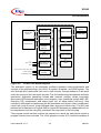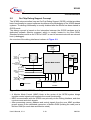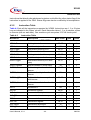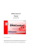
1
User’s Manual, V 0.1, Jan 2005
XC800
Microcontroller Family
Architecture and Instruction Set
Microcontrollers
N e v e r
s t o p
t h i n k i n g .
Edition 2005-01
Published by Infineon Technologies AG,
St.-Martin-Strasse 53,
81669 München, Germany
© Infineon Technologies AG 2005.
All Rights Reserved.
Attention please!
The information herein is given to describe certain components and shall not be considered as a guarantee of
characteristics.
Terms of delivery and rights to technical change reserved.
We hereby disclaim any and all warranties, including but not limited to warranties of non-infringement, regarding
circuits, descriptions and charts stated herein.
Information
For further information on technology, delivery terms and conditions and prices please contact your nearest
Infineon Technologies Office (www.infineon.com).
Warnings
Due to technical requirements components may contain dangerous substances. For information on the types in
question please contact your nearest Infineon Technologies Office.
Infineon Technologies Components may only be used in life-support devices or systems with the express written
approval of Infineon Technologies, if a failure of such components can reasonably be expected to cause the failure
of that life-support device or system, or to affect the safety or effectiveness of that device or system. Life support
devices or systems are intended to be implanted in the human body, or to support and/or maintain and sustain
and/or protect human life. If they fail, it is reasonable to assume that the health of the user or other persons may
be endangered.
User’s Manual, V 0.1, Jan 2005
XC800
Microcontroller Family
Architecture and Instruction Set
Microcontrollers
N e v e r
s t o p
t h i n k i n g .
XC800
Revision History:
2005-01
Previous Version:
-
Page
V 0.1
Subjects (major changes since last revision)
We Listen to Your Comments
Any information within this document that you feel is wrong, unclear or missing at all?
Your feedback will help us to continuously improve the quality of this document.
Please send your proposal (including a reference to this document) to:
[email protected]
XC800
Table of Contents
Page
1
1.1
1.2
1.3
1.3.1
1.3.1.1
1.3.1.2
1.3.2
1.3.3
1.3.3.1
1.3.3.2
1.3.3.3
1.3.4
1.3.4.1
1.3.4.2
1.4
Fundamental Structure . . . . . . . . . . . . . . . . . . . . . . . . . . . . . . . . . . . . . . . 1
Foreword . . . . . . . . . . . . . . . . . . . . . . . . . . . . . . . . . . . . . . . . . . . . . . . . . . . 1
Introduction . . . . . . . . . . . . . . . . . . . . . . . . . . . . . . . . . . . . . . . . . . . . . . . . . 1
Memory Organization . . . . . . . . . . . . . . . . . . . . . . . . . . . . . . . . . . . . . . . . . 2
Memory Extension . . . . . . . . . . . . . . . . . . . . . . . . . . . . . . . . . . . . . . . . . . 3
Memory Extension Stack . . . . . . . . . . . . . . . . . . . . . . . . . . . . . . . . . . . 3
Memory Extension Effects . . . . . . . . . . . . . . . . . . . . . . . . . . . . . . . . . . 3
Program Memory . . . . . . . . . . . . . . . . . . . . . . . . . . . . . . . . . . . . . . . . . . . 5
Data Memory . . . . . . . . . . . . . . . . . . . . . . . . . . . . . . . . . . . . . . . . . . . . . . 5
Internal Data Memory . . . . . . . . . . . . . . . . . . . . . . . . . . . . . . . . . . . . . 5
Internal Data Memory XRAM . . . . . . . . . . . . . . . . . . . . . . . . . . . . . . . . 6
External Data Memory . . . . . . . . . . . . . . . . . . . . . . . . . . . . . . . . . . . . . 6
Registers . . . . . . . . . . . . . . . . . . . . . . . . . . . . . . . . . . . . . . . . . . . . . . . . . 6
Special Function Register Extension by Mapping . . . . . . . . . . . . . . . . 7
Special Function Register Extension by Paging . . . . . . . . . . . . . . . . . 8
Bit Protection Scheme . . . . . . . . . . . . . . . . . . . . . . . . . . . . . . . . . . . . . . . . 11
2
2.1
2.1.1
2.1.2
2.1.3
2.1.4
2.1.5
2.1.6
2.1.7
2.1.8
2.1.9
2.1.10
2.1.11
2.2
2.3
2.3.1
2.3.2
2.4
2.5
CPU Architecture . . . . . . . . . . . . . . . . . . . . . . . . . . . . . . . . . . . . . . . . . . . . 1
CPU Register Description . . . . . . . . . . . . . . . . . . . . . . . . . . . . . . . . . . . . . . 4
Stack Pointer (SP) . . . . . . . . . . . . . . . . . . . . . . . . . . . . . . . . . . . . . . . . . . 4
Data Pointer (DPTR) . . . . . . . . . . . . . . . . . . . . . . . . . . . . . . . . . . . . . . . . 4
Accumulator (ACC) . . . . . . . . . . . . . . . . . . . . . . . . . . . . . . . . . . . . . . . . . 4
B Register . . . . . . . . . . . . . . . . . . . . . . . . . . . . . . . . . . . . . . . . . . . . . . . . 4
Program Status Word . . . . . . . . . . . . . . . . . . . . . . . . . . . . . . . . . . . . . . . 5
Extended Operation Register (EO) . . . . . . . . . . . . . . . . . . . . . . . . . . . . . 6
Memory Extension Registers . . . . . . . . . . . . . . . . . . . . . . . . . . . . . . . . . . 7
Power Control Register (PCON) . . . . . . . . . . . . . . . . . . . . . . . . . . . . . . . 9
UART Registers . . . . . . . . . . . . . . . . . . . . . . . . . . . . . . . . . . . . . . . . . . . 10
Timer/Counter Registers . . . . . . . . . . . . . . . . . . . . . . . . . . . . . . . . . . . . 12
Interrupt Registers . . . . . . . . . . . . . . . . . . . . . . . . . . . . . . . . . . . . . . . . . 14
On-Chip Debug Support Concept . . . . . . . . . . . . . . . . . . . . . . . . . . . . . . . 18
Basic Interrupt Handling . . . . . . . . . . . . . . . . . . . . . . . . . . . . . . . . . . . . . . 20
Interrupt Source and Vector Address . . . . . . . . . . . . . . . . . . . . . . . . . . 20
Interrupt Handling . . . . . . . . . . . . . . . . . . . . . . . . . . . . . . . . . . . . . . . . . 20
Interrupt Response Time . . . . . . . . . . . . . . . . . . . . . . . . . . . . . . . . . . . . . . 21
Service Order . . . . . . . . . . . . . . . . . . . . . . . . . . . . . . . . . . . . . . . . . . . . . . . 22
3
3.1
3.2
3.2.1
3.2.2
CPU Timing . . . . . . . . . . . . . . . . . . . . . . . . . . . . . . . . . . . . . . . . . . . . . . . .
Instruction Timing . . . . . . . . . . . . . . . . . . . . . . . . . . . . . . . . . . . . . . . . . . . .
Accessing External Memory . . . . . . . . . . . . . . . . . . . . . . . . . . . . . . . . . . . .
Accessing External Program Memory . . . . . . . . . . . . . . . . . . . . . . . . . . .
Accessing External Data Memory . . . . . . . . . . . . . . . . . . . . . . . . . . . . . .
User’s Manual, V 0.1
I-1
1
1
3
3
4
2005-01
XC800
Table of Contents
4
4.1
4.2
4.3
4.3.1
4.3.2
4.3.3
Page
Instruction Set . . . . . . . . . . . . . . . . . . . . . . . . . . . . . . . . . . . . . . . . . . . . . . 1
Addressing Modes . . . . . . . . . . . . . . . . . . . . . . . . . . . . . . . . . . . . . . . . . . . . 1
Introduction to the Instruction Set . . . . . . . . . . . . . . . . . . . . . . . . . . . . . . . . 3
Instructions . . . . . . . . . . . . . . . . . . . . . . . . . . . . . . . . . . . . . . . . . . . . . . . . . 5
Affected Flags . . . . . . . . . . . . . . . . . . . . . . . . . . . . . . . . . . . . . . . . . . . . . 5
Instruction Table . . . . . . . . . . . . . . . . . . . . . . . . . . . . . . . . . . . . . . . . . . . 6
Instruction Definitions . . . . . . . . . . . . . . . . . . . . . . . . . . . . . . . . . . . . . . 11
User’s Manual, V 0.1
I-2
2005-01
XC800
Fundamental Structure
1
Fundamental Structure
1.1
Foreword
This manual provides an overview of the architecture and functional characteristics of
the XC800 microcontroller family. It also includes a complete description of the XC800
core instruction set. For detailed information on the different derivatives of the XC800 8bit microcontrollers, refer to the respective user’s manuals.
1.2
Introduction
The Infineon XC800 microcontroller family has a CPU which is functionally upward
compatible to the 8051. While the standard 8051 core is designed around a 12-clock
machine cycle, the XC800 core uses a two-clock period machine cycle.
The instruction set consists of 45% one-byte, 41% two-byte, and 14% three-byte
instructions. Each instruction takes 1, 2 or 4 machine cycles to execute. In case of
access to slower memory, the access time may be extended by wait states.
The XC800 microcontrollers support via the dedicated JTAG interface or the standard
UART interface, a range of debugging features including basic stop/start, single-step
execution, breakpoint support and read/write access to the data memory, program
memory and special function registers.
The key features of the XC800 microcontrollers are listed below.
Features:
•
•
•
•
•
•
•
•
•
•
•
•
Two clocks per machine cycle
Program memory download option
Up to 1 Mbyte of external data memory; up to 256 bytes of internal data memory
Up to 1 Mbyte of program memory
Wait state support for slow memory
Support for synchronous or asynchronous program and data memory
15-source, 4-level interrupt controller
Up to eight data pointers
Power saving modes
Dedicated debug mode via the standard JTAG interface or UART
Two 16-bit timers (Timer 0 and Timer 1)
Full-duplex serial port (UART)
User’s Manual, V 0.1
1-1
2005-01
XC800
Fundamental Structure
1.3
Memory Organization
The memory partitioning of the XC800 microcontrollers is typical of the Harvard
architecture where data and program areas are held in separate memory space. The
on-chip peripheral units are accessed using an internal Special Function Register (SFR)
memory area that occupies 128 bytes of address, which can be mapped or paged to
increase the number of addressable SFRs.
A typical memory map of the code space consists of internal ROM/Flash, on-chip Boot
ROM, an on-chip XRAM and/or external memory. The memory map of the data space is
typical of the standard 8051 architecture: the internal data memory consists of 128 bytes
of directly addressable Internal RAM (IRAM), 128 bytes of indirect addressable IRAM
and an ‘external’ RAM (XRAM). External data memory may be supported outside of the
internal range. Figure 1-1 provides a general overview of the XC800 memory space and
a typical memory map in user mode.
Bank F
Bank E
Bank D
Bank C
Bank B
Bank A
Bank 9
Bank 8
Bank 7
Bank 6
Bank 5
Bank 4
Bank 3
Bank 2
Bank 1
XRAM
F' FFFF H
F' 0000H
E' FFFF H
E' 0000H
D' FFFF H
D' 0000H
C' FFFF H
C' 0000H
B' FFFF H
B' 0000H
A' FFFF H
A' 0000H
9' FFFFH
9' 0000H
8' FFFFH
8' 0000H
7' FFFFH
7' 0000H
6' FFFFH
6' 0000H
5' FFFFH
5' 0000H
4' FFFFH
4' 0000H
3' FFFFH
3' 0000H
2' FFFF H
2' 0000H
1' FFFF H
1' 0000H
0' FFFF H
Bank E
Bank D
Bank C
Bank B
Bank A
Bank 9
Bank 8
Bank 7
Bank 6
Bank 5
Bank 4
Bank 3
Bank 2
Bank 1
XRAM
0' F000H
Reserved
Boot ROM
B ank 0
Notes:
! XC800 supports memory extension of up to 1 Mbyte
program memory and 1 Mbyte external data memory.
This is accomplished by sixteen 64K bank blocks. At any
one time, only one bank of the respective memory is
active.
! In case of implemented memory extension, an additional
extension stack RAM is added on-chip and located from
80H to FF H. This memory is not accessible by software.
! The smallest memory space without memory extension
is such that only Bank 0 is available.
! In general, the data space where the corresponding
code space is occupied by internal memory is reserved.
! If supported by available pins, external memory may be
located at regions not occupied by internal memory.
Program Memory : In general, #EA = 1 selects dynamic
fetch from internal and external program memory; #EA =
0 selects to always fetch from external program memory
instead of Internal Memory .
Data Memory : External data is accessed by the MOVX
instruction.
! This memory mapping is general for user mode. Refer to
respective user’s manuals for exact mappings for
specific device.
Bank F
Memory Extension
Stack Pointer
(MEXSP)
Indirect
Address
Direct
Address
Internal RAM
Special Function
Registers
0' C000H
FF H
Extension Stack RAM
80H
Internal Memory
7FH
Reserved
Internal RAM
0' 0000H
Code Space
Figure 1-1
00 H
External Data Space
Internal Data Space
XC800 Memory Space and Typical Memory Map in user mode
User’s Manual, V 0.1
1-2
V 1.0, 2005-01
XC800
Fundamental Structure
In derivatives with memory extension, an additional 128 bytes of memory extension
stack RAM is available from 80H to FFH. Access to this memory is only possible by the
hardware, so the memory is effectively transparent to the user. By default after reset, the
memory extension stack pointer (MEXSP) points to 7FH. It is pre-incremented by call
instructions and post-decremented by return instructions.
1.3.1
Memory Extension
The standard amount of addressable program or external data memory in an 8051
system is 64 Kbytes. The XC800 core supports memory expansion of up to 1 Mbyte and
this is enabled by the availability of a Memory Management Unit (MMU) and a Memory
Extension Stack. The MMU adds a set of Memory Extension registers (MEX1, MEX2,
and MEX3) to control access to the extended memory space by different addressing
modes. The Memory Extension Stack is used by the hardware to ‘push’ and ‘pop’ values
of MEX1.
Program Code is always fetched from the 64-Kbyte block pointed to by the 4-bit Current
Bank (CB) register bit field. It is updated from a 4-bit Next Bank (NB) bit field upon
execution of long jump (LJMP) and call instructions. CB and NB together constitute the
MEX1 register. The programmer simply writes the new bank number to NB before a jump
or call instruction.
Interrupt service routines are always executed from code in the 64-Kbyte block pointed
to by the Interrupt Bank (IB) register bit field. Further, memory constant data reads (in
code space) and external data accesses may take place in banks other than the current
bank. These banks are pointed to by the Memory Constant Bank pointer (MCB) and
XRAM Bank pointer (MX). These bit fields are located in MEX2 and MEX3 registers.
1.3.1.1
Memory Extension Stack
Interrupts and Calls in Memory Extension mode make use of a Memory Extension Stack,
which is updated at the same time as the standard stack.
The Memory Extension Stack is addressed using the SFR Memory Extension Stack
Pointer MEXSP. This read/write register provides for a stack depth of up to 128 bytes
(Bit 7 is always 0). The SFR is pre-incremented by each call instruction that is executed,
and post-decremented by return instructions. MEXSP is by default reset to 7FH so that
the first increment selects the bottom of the stack. No indication of stack overflow is
provided.
1.3.1.2
Memory Extension Effects
The following instructions can change the 64-Kbyte block pointed to: MOVC, MOVX,
LJMP, LCALL, ACALL, RET, and RETI.
User’s Manual, V 0.1
1-3
2005-01
XC800
Fundamental Structure
Relative jumps (SJMP etc.) and absolute jumps within 2-Kbyte regions (AJMPs),
however, will in no way change the current bank. In other words, these instructions do
not deselect the active 64-Kbyte bank block.
Move Constant Instructions (MOVC)
MOVC instructions access data bytes in either the Current bank (CB19 – CB16) or a
‘Memory Constant’ bank, defined by the MCB19 – MCB16 bit field in MEX3 and MEX2.
The bank selection is done by the MCM bit in MEX2 (MEX2.7).
Move External Data Instructions (MOVX)
MOVX instructions can either access data in the Current bank or a ‘Data Memory’ bank,
defined by the MX19 – MX16 bits in MEX3. The bank selection is done by the MXM bit
in MEX3 (MEX3.3).
Long Jump Instructions (LJMP)
When a jump to another bank of the Memory Extension is required, the Next Bank bits
NB19 – NB16 in MEX1 (MEX1.3 – MEX1.0) must be set to the appropriate bank address
before the LJMP instruction is executed. When the LJMP is encountered in the code, the
Next Bank bits (NB19 – 16) are copied to the Current Bank bits CB19 – CB16 in MEX1
(MEX1.7 – MEX1.4) and appear on address bus at the beginning of the next program
fetch cycle.
Note: The Next Bank Bits (NB19 – 16) are not changed by the jump.
CALL Instructions (LCALL and ACALL)
Whenever an LCALL occurs, the MMU carries out the following sequence of actions:
1. The Memory Extension Stack Pointer is incremented.
2. The MEX1 register bits are made available on data bus.
3. The MEXSP register bits [6:0] are made available on address lines.
4. The Memory Extension Stack read and write signals are set for a write operation.
5. A write is performed to the Memory Extension Stack.
6. The Next Bank bits NB19 – NB16 (MEX1.3 – MEX1.0) are copied to the CB19 – CB16
bits (MEX1.7 – MEX.4).
Return Instructions (RET and RETI)
On leaving a subroutine, the MMU carries out the following sequence of actions:
1. The MEXSP register bits [6:0] are made available on address.
2. The Memory Extension Stack read and write signals are set for a read operation.
3. A read is performed on the Memory Extension Stack.
4. Memory Extension Stack data is written to the MEX1 register.
5. The Memory Extension Stack Pointer is decremented.
User’s Manual, V 0.1
1-4
V 1.0, 2005-01
XC800
Fundamental Structure
1.3.2
Program Memory
Up to 1 Mbyte of synchronous or asynchronous internal and/or external program
memory is supported. Program memory extension, if supported by the XC800 derivative,
is accomplished with a 4-bit Current Bank pointer (CB). The program code is fetched
from the 64-Kbyte block pointed to by CB. The minimum supported code space is
therefore 64 Kbytes.
If the internal program memory is used, the EA (External Access) pin must be held at
high level. With EA held high, the microcontroller executes instructions internally unless
the address (Program Counter) is outside the range of the internal program memory. In
this case, dynamic code fetch from internal and external program memory is supported
if the external memory bus is available on the derivative. If the EA pin is held at low level,
the microcontroller executes program code from external program memory, instead of
from internal memory. The general exception is for accesses to address ranges of the
active Boot ROM, internal XRAM and code-space data (e.g., Data Flash), where fetch is
always from the internal memory regardless of the status of EA pin.
Most XC800 derivatives include a section for Boot ROM code, the size of which depends
on the derivative. Usually, the Boot ROM code is executed first after reset where the Boot
ROM is mapped starting from base address 0000H of the code space. The Boot ROM
code will switch the memory mapping so that before control is passed to the user code,
the standard memory map (of the derivative) is active where user code could run starting
from address 0000H.
For program memory implemented as RAM, the XC800 core supports write to program
memory with the instruction MOVC @(DPTR++),A. This is generally supported by the
XC800 derivatives for writes to internal memory only.
1.3.3
Data Memory
The data memory space consists of internal and external memory portions. The internal
data memory area is addressed using 8-bit addresses. The external data memory and
the internal XRAM data memory are addressable by 8-bit or 16-bit indirect address with
‘MOVX’, additionally with up to 4-bit for selection of extended memory bank (maximum
1 Mbyte).
1.3.3.1
Internal Data Memory
The internal data memory is divided into two physically separate and distinct blocks: the
256-byte RAM and the 128-byte SFR area. While the upper 128 bytes of RAM and the
SFR area share the same address locations, they are accessed through different
addressing modes. The lower 128 bytes of RAM can be accessed through either direct
or register indirect addressing while the upper 128 bytes of RAM can be accessed
through register indirect addressing only. The special function registers are accessible
through direct addressing.
User’s Manual, V 0.1
1-5
2005-01
XC800
Fundamental Structure
The 16 bytes of RAM that occupy addresses from 20H to 2FH are bitaddressable. Bit 0
of the internal data byte at 20H has the bit address 00H, while bit 7 of the internal data
byte at 2FH has the bit address 7FH.
By default after reset, the stack pointer points to address 07H. The stack may reside
anywhere in the internal RAM.
RAM occupying direct addresses from 30H to 7FH can be used as scratch pad.
1.3.3.2
Internal Data Memory XRAM
The size of the internal XRAM is not fixed and varies depending on XC800 derivative.
The internal XRAM is mapped to both the external data space and the code space
because it can be accessed using both ‘MOVX’ and ‘MOVC’ instructions. When
accessed using the 8-bit MOVX instruction via register R0 or R1, the SFR XADDRH
must be initialized to specify the upper address byte.
The internal XRAM can be enabled or disabled. If disabled, external data memory can
be accessed in the address range of the internal XRAM, with activated external data
memory signals. If enabled, the external data memory signals are not generated when
the internal XRAM is accessed. Therefore, the corresponding ports can be used as
general purpose I/O in an application where there is no access to off-chip external data/
program memory.
1.3.3.3
External Data Memory
Up to 1 Mbyte of synchronous or asynchronous external data memory is supported.
External data memory extension, if supported by the XC800 derivative, is accomplished
with either the 4-bit Current Bank pointer (CB) or the 4-bit XRAM Bank pointer (MX),
selected by the MXM bit. The data is fetched from the 64-Kbyte block pointed to by CB
or MX. Some XC800 derivatives may not support external data memory.
1.3.4
Registers
All registers, except the program counter and the four general purpose register banks,
reside in the SFR area.
The lower 32 locations of the internal lower data RAM are assigned to four banks with
eight general purpose registers (GPRs) each. At any one time, only one of these banks
can be enabled by two bits in the program status word (PSW): RS0 (PSW.3) and RS1
(PSW.4). This allows fast context switching, which is useful when entering subroutines
or interrupt service routines. The eight general purpose registers of the selected register
bank may be accessed by register addressing. For indirect addressing modes, the
registers R0 and R1 are used as pointer or index register to address internal or external
memory.
User’s Manual, V 0.1
1-6
V 1.0, 2005-01
XC800
Fundamental Structure
The Special Function Registers (SFRs) are mapped to the internal data space in the
range 80H to FFH. The SFRs are accessible through direct addressing. The SFRs that
are located at addresses with address bit 0-2 equal to 0 (addresses 80H, 88H, 90H, ...,
F8H) are bitaddressable. Each bit of the bitaddressable SFRs has bit address
corresponding to the SFR byte address and its position within the SFR byte. For
example, bit 7 of SFR at byte address 80H has a bit address of 87H. The bit addresses
of the SFR bits span from 80H to FFH.
As the 128-SFR range is less than the total number of registers required, register
extension mechanisms are implemented to increase the number of addressable SFRs.
These mechanisms include:
• Mapping
• Paging
1.3.4.1
Special Function Register Extension by Mapping
SFR extension is performed at the system level by mapping. The SFR area is extended
into two portions: the standard (non-mapped) SFR area and the mapped SFR area.
Each portion supports the same address range 80H to FFH, bringing the number of
addressable SFRs to 256. To access SFRs in the mapped area, bit RMAP in SFR
SYSCON0 must be set by software. The mapped SFR area provides the same
addressing capabilities (direct addressing, bit addressing) as the standard SFR area. Bit
RMAP must be cleared by software to access the SFRs in the standard area. The
hardware does not automatically clear/set the bit.
SYSCON0
System Control Register 0
7
6
Reset Value: XXXX XXX0B
5
4
3
2
1
0
-
RMAP
-
rw
The functions of the shaded bits are not described here
Field
Bits
Type Description
RMAP
0
rw
User’s Manual, V 0.1
Special Function Register Map Control
0
The access to the standard SFR area is
enabled.
1
The access to the mapped SFR area is
enabled.
1-7
2005-01
XC800
Fundamental Structure
1.3.4.2
Special Function Register Extension by Paging
The number of SFRs may be further extended for some on-chip peripherals at the
module level via a paging scheme. These peripherals have a built-in local SFR extension
mechanism for increasing the number of addressable SFRs. The control is via bit field
PAGE in the module page register MOD_PAGE. The bit field PAGE must be
programmed before accessing the SFR of the target module. Each module may contain
different number of pages and different number of SFRs per page, depending on the
requirement. Besides setting the correct RMAP bit value to select the standard or
mapped SFR area, the user must also ensure that a valid PAGE is selected to access
the desired SFR. The paging mechanism is illustrated in Figure 1-2.
SFR Address
(from CPU)
PAGE 0
MOD_PAGE.PAGE
SFR0
rw
SFR1
…...
SFRx
PAGE 1
SFR0
SFR Data
(to/from CPU)
SFR1
…...
SFRy
…...
PAGE q
SFR0
SFR1
…...
SFRz
Module
Figure 1-2
SFR Extension by Paging
If an interrupt routine is initiated between the page register access and the module
register access, and the interrupt must access a register located in another page, the
current page setting can be saved, the new one programmed and finally, the old page
setting restored. This is possible with the storage fields STx (x = 0 - 3) for the save and
restore action of the current page setting, as illustrated in Figure 1-3. By indicating which
User’s Manual, V 0.1
1-8
V 1.0, 2005-01
XC800
Fundamental Structure
storage register should be used in parallel with the new page value, a single write
operation can:
• Save the contents of PAGE in STx before overwriting with the new value
(this is done in the beginning of the interrupt routine to save the current page setting
and program the new page number); or
• Overwrite the contents of PAGE with the contents of STx, ignoring the value written to
the bit positions of PAGE
(this is done at the end of the interrupt routine to restore the previous page setting
before the interrupt occurred)
ST3
ST2
ST1
ST0
STNR
PAGE
value update
from CPU
Figure 1-3
Storage Elements for Paging
With this mechanism, a certain number of interrupt routines (or other routines) can
perform page changes without reading and storing the previously used page information.
The use of only write operations makes the system simpler and faster. Consequently,
this mechanism significantly improves the performance of short interrupt routines.
The page register has the following definition:
MOD_PAGE
Page Register for module MOD
7
6
5
Reset Value: 00H
4
3
2
1
OP
STNR
0
PAGE
w
w
r
rw
User’s Manual, V 0.1
1-9
0
2005-01
XC800
Fundamental Structure
Field
Bits
Type Description
PAGE
[2:0]
rw
Page Bits
When written, the value indicates the new page.
When read, the value indicates the currently active
page.
STNR
[5:4]
w
Storage Number
This number indicates which storage bit field is the
target of the operation defined by bit field OP.
If OP = 10B,
the contents of PAGE are saved in STx before being
overwritten with the new value.
If OP = 11B,
the contents of PAGE are overwritten by the
contents of STx. The value written to the bit positions
of PAGE is ignored.
00
01
10
11
ST0 is selected.
ST1 is selected.
ST2 is selected.
ST3 is selected.
OP
[7:6]
w
Operation
0X Manual page mode. The value of STNR is
ignored and PAGE is directly written.
10
New page programming with automatic page
saving. The value written to the bit field PAGE
is stored. In parallel, the previous contents of
PAGE are saved in the storage bit field STx
indicated by STNR.
11
Automatic restore page action. The value
written to the bit field PAGE is ignored and
instead, PAGE is overwritten by the contents
of the storage bit field STx indicated by STNR.
0
3
r
Reserved
Returns 0 if read; should be written with 0.
User’s Manual, V 0.1
1-10
V 1.0, 2005-01
XC800
Fundamental Structure
1.4
Bit Protection Scheme
The bit protection scheme prevents direct software writing of selected bits (i.e., protected
bits) by the PASSWD register. When the bit field MODE is 11B, writing 10011B to the bit
field PASS opens access to writing of all protected bits and writing 10101B to the bit field
PASS closes access to writing of all protected bits. Note that access is opened for
maximum 32 CCLKs if the “close access” password is not written. If “open access”
password is written again before the end of 32 CCLK cycles, there will be a recount of
32 CCLK cycles.
The bits or bit fields that are protected may differ for the XC800 derivatives.
PASSWD
Password Register
7
Reset Value: 07H
6
5
4
3
2
1
0
PASS
PROTECT
_S
MODE
wh
rh
rw
Field
Bits
Type Description
MODE
[1:0]
rw
Bit-Protection Scheme Control bit
00
Scheme Disabled
11
Scheme Enabled (default)
Others: Scheme Enabled
These two bits cannot be written directly. To change
the value between 11B and 00B, the bit field PASS
must be written with 11000B, only then will the
MODE[1:0] be registered.
PROTECT_S
2
rh
Bit-Protection Signal Status bit
This bit shows the status of the protection.
0
Software is able to write to all protected bits.
1
Software is unable to write to any protected
bits.
PASS
[7:3]
wh
Password bits
The Bit-Protection Scheme recognizes only three
patterns.
11000B Enables writing of the bit field MODE.
10011B Opens access to writing of all protected bits.
10101B Closes access to writing of all protected bits.
User’s Manual, V 0.1
1-11
2005-01
XC800
CPU Architecture
2
CPU Architecture
Figure 2-1 depicts the typical architecture of an XC800 family microcontroller. It
includes the main functional blocks and standard units. The units represented by dotted
boxes may not be available, depending on the derivative; these include peripheral units
and external memory bus. Memory sizes vary depending on the XC800 microcontroller
derivative.
Internal Bus
Boot ROM
External
Data
Memory
External
Code
Memory
XC800 Core
Internal Data
RAM
UART
CAN
CCU6
MDU
SSC
Cordic
Timer 2
XRAM
Flash
or
ROM
System Control
Unit
Po rts
RESET
VDDP
VSSP
VDDC
VSSC
T0 & T1
VAREF
VAGND
ADC
Watchdog
Timer
OCDS 1)
XTAL1
XTAL2
Figure 2-1
OSC
& PLL
Standard JTAG I/O
1)
OCDS: On-Chip Debug
Support
Typical Architecture of XC800 Family Microcontroller
The CPU functional blocks are shown in Figure 2-2. The CPU consists mainly of the
instruction decoder, the arithmetic section, the program control section, the access
control section, and the interrupt controller. The CPU also provides modes for power
saving.
The instruction decoder decodes each instruction and accordingly generates the internal
signals required to control the functions of the individual units within the CPU. These
internal signals have an effect on the source and destination of signal transfers and
control the ALU processing.
User’s Manual, V 0.1
2-1
2005-01
XC800
CPU Architecture
Internal Data
Memory
Core SFRs
Register Interface
External Data
Memory
External SFRs
16-bit Registers &
Memory Interface
ALU
Opcode &
Immediate
Registers
Multiplier / Divider
Opcode Decoder
Timers / Counters
State Machine &
Power Saving
UART
Program Memory
fCCLK
Memory Wait
Reset
Legacy External Interrupts (IEN0, IEN1)
External Interrupts
Non-Maskable Interrupt
Figure 2-2
Interrupt
Controller
XC800 Core Block Diagram
The arithmetic section of the processor performs extensive data manipulation and
consists of the arithmetic/logic unit (ALU), A register, B register, and PSW register. The
ALU accepts 8-bit data words from one or two sources, and generates an 8-bit result
under the control of the instruction decoder. The ALU performs both arithmetic and logic
operations. Arithmetic operations include add, subtract, multiply, divide, increment,
decrement, BCD-decimal-add-adjust, and compare. Logic operations include AND, OR,
Exclusive OR, complement, and rotate (right, left, or swap nibble (left four)). Also
included is a Boolean unit performing the bit operations such as set, clear, complement,
jump-if-set, jump-if-not-set, jump-if-set-and-clear, and move to/from carry. The ALU can
perform the bit operations of logical AND or logical OR between any addressable bit (or
its complement) and the carry flag, and place the new result in the carry flag.
The program control section controls the sequence in which the instructions stored in
program memory are executed. The 16-bit program counter (PC) holds the address of
User’s Manual, V 0.1
2-2
2005-01
XC800
CPU Architecture
the next instruction to be executed. The conditional branch logic enables internal and
external events to the processor to cause a change in the program execution sequence.
The access control unit is responsible for the selection of the on-chip memory resources.
The interrupt requests from the peripheral units are handled by the interrupt controller
unit.
User’s Manual, V 0.1
2-3
2005-01
XC800
CPU Architecture
2.1
CPU Register Description
The CPU registers occupy direct Internal Data Memory space locations in the range 80H
to FFH.
2.1.1
Stack Pointer (SP)
The SP register contains the Stack Pointer. The Stack Pointer is used to load the
program counter into Internal Data Memory during LCALL and ACALL instructions, and
to retrieve the program counter from memory during RET and RETI instructions. Data
may also be saved on or retrieved from the stack using PUSH and POP instructions.
Instructions that use the stack automatically pre-increment or post-decrement the stack
pointer so that the stack pointer always points to the last byte written to the stack, i.e. the
top of the stack. On reset, the Stack Pointer is reset to 07H. This causes the stack to
begin at a location = 08H above register bank zero. The SP can be read or written under
software control. The programmer must ensure that the location and size of the stack in
internal data memory do not interfere with other application data.
2.1.2
Data Pointer (DPTR)
The Data Pointer (DPTR) is stored in registers DPL (Data Pointer Low byte) and DPH
(Data Pointer High byte) to form 16-bit addresses for External Data Memory accesses
and
MOVX @DPTR,A),
for
program
byte
moves
(MOVX A,@DPTR
(MOVC A,@A+DPTR), and for indirect program jumps (JMP @A+DPTR).
Two true 16-bit operations are allowed on the Data Pointer: load immediate
(MOV DPTR,#data) and increment (INC DPTR).
The CPU can support up to 8 data pointers. This helps programming in high level
languages, which may require the storing of data in large external data memory portions.
Selection of the active data pointer is done via the SFR EO (see Section 2.1.6). The
number of data pointers available is specific to the XC800 derivative.
2.1.3
Accumulator (ACC)
This register is an operand for most ALU operations. ACC is the symbol for the
accumulator register. The mnemonics for accumulator-specific instructions, however,
refer to the accumulator simply as “A”.
2.1.4
B Register
The B register is used during multiply and divide operations to provide the second
operand. For other instructions, it can be treated as another scratch pad register.
User’s Manual, V 0.1
2-4
2005-01
XC800
CPU Architecture
2.1.5
Program Status Word
The Program Status Word (PSW) contains several status bits that reflect the current
state of the CPU.
PSW
Program Status Word Register
Reset Value: 00H
7
6
5
4
3
2
1
0
CY
AC
F0
RS1
RS0
OV
F1
P
rw
rwh
rwh
rw
rw
rwh
rwh
rh
Field
Bits
Type Description
P
0
rh
Parity Flag
Set/cleared by hardware after each instruction to
indicate an odd/even number of “one” bits in the
accumulator, i.e., even parity.
F1
1
rwh
General Purpose Flag
OV
2
rwh
Overflow Flag
Used by arithmetic instructions
RS0
RS1
3
4
rw
Register Bank Select
These bits are used to select one of the four register
banks.
RS1 RS0 Function
0
0
Bank 0 selected, data address 00H-07H
0
1
Bank 1 selected, data address 08H-0FH
1
0
Bank 2 selected, data address 10H-17H
1
1
Bank 3 selected, data address 18H-1FH
F0
5
rwh
General Purpose Flag
AC
6
rwh
Auxiliary Carry Flag
Used by instructions that execute BCD operations
CY
7
rw
Carry Flag
Used by arithmetic instructions
User’s Manual, V 0.1
2-5
2005-01
XC800
CPU Architecture
2.1.6
Extended Operation Register (EO)
The EO register has two functions. One function is to select the active data pointer where
the derivative has multiple data pointers. The other function is to select the instruction
executed on opcode A5H. The active instruction is either TRAP or
MOVC @(DPTR++),A.
EO
Extended Operation Register
7
6
5
Reset Value: 00H
4
3
2
1
0
TRAP_EN
0
DPSEL
r
rw
r
rw
Field
Bits
Type Description
DPSEL
[2:0]
rw
Data Pointer Select
000 DPTR0 selected
001 DPTR1 selected (if available)
010 DPTR2 selected (if available)
011 DPTR3 selected (if available)
100 DPTR4 selected (if available)
101 DPTR5 selected (if available)
110 DPTR6 selected (if available)
111 DPTR7 selected (if available)
TRAP_EN
4
rw
TRAP Enable
0
Select MOVC @(DPTR++),A
1
Select software TRAP instruction
0
3,
[7:5]
r
Reserved
Returns 0 if read; should be written with 0.
User’s Manual, V 0.1
2-6
0
2005-01
XC800
CPU Architecture
2.1.7
Memory Extension Registers
These registers support the memory extension feature, which may not be available on
certain XC800 microcontroller derivatives.
MEX1
Memory Extension Register 1
7
6
5
Reset Value: 00H
4
3
2
1
CB[19:16]
NB[19:16]
rh
rw
Field
Bits
Type Description
NB[19:16]
[3:0]
rw
Next Bank Number
CB[19:16]
[7:4]
rh
Current Bank Number
MEX2
Memory Extension Register 2
7
6
5
0
Reset Value: 00H
4
3
2
1
MCM
MCB[18:16]
IB[19:16]
rw
rw
rw
0
Field
Bits
Type Description
IB[19:16]
[3:0]
rw
Interrupt Bank Number
MCB[18:16]
[6:4]
rw
Memory Constant Bank Number (with MEX3.7)
MCM
7
rw
Memory Constant Mode
0
MOVC access data in the current bank
1
MOVC access data in the Memory Constant
bank
User’s Manual, V 0.1
2-7
2005-01
XC800
CPU Architecture
MEX3
Memory Extension Register 3
7
6
5
Reset Value: 00H
4
3
2
1
MCB19
0
MX19
MXM
MX[18:16]
rw
r
rw
rw
rw
0
Field
Bits
Type Description
MX[19:16]
[2:0],
4
rw
XRAM Bank Number
MXM
3
rw
XRAM Bank Selector
0
MOVX access data in the current bank
1
MOVX access data in the Memory XRAM
bank
MCB19
7
rw
Memory Constant Bank Number MSB
0
[6:5]
r
Reserved
Returns 0 if read; should be written with 0.
MEXSP
Memory Extension Stack Pointer Register
7
6
5
Reset Value: 7FH
4
3
0
MXSP
r
rw
2
1
0
Field
Bits
Type Description
MXSP
[6:0]
rw
Memory Extension Stack Pointer
It provides for a stack depth of up to 128 bytes. It is
pre-incremented by call instructions and postdecremented by return instructions.
0
7
r
Reserved
Returns 0 if read; should be written with 0.
User’s Manual, V 0.1
2-8
2005-01
XC800
CPU Architecture
2.1.8
Power Control Register (PCON)
The XC800 CPU has two power saving modes: idle mode and power-down mode. In idle
mode, the clock to the CPU is disabled while other peripherals may continue to run
(possibly at lower frequency). In power-down mode, the clock to the entire CPU is
stopped.
PCON
Power Control Register
7
6
Reset Value: 00H
5
4
3
2
1
0
SMOD
0
GF1
GF0
0
IDLE
rw
r
rw
rw
r
rw
Field
Bits
Type Description
IDLE
0
rw
Idle Mode Enable
0
Do not enter idle mode
1
Enter idle mode
GF0
2
rw
General Purpose Flag Bit 0
GF1
3
rw
General Purpose Flag Bit 1
SMOD
7
rw
Double Baud Rate Enable
0
Do not double the baud rate of serial interface
in mode 2
1
Double baud rate of serial interface in mode 2
0
1,
[6:4]
r
Reserved
Returns 0 if read; should be written with 0.
User’s Manual, V 0.1
2-9
2005-01
XC800
CPU Architecture
2.1.9
UART Registers
The UART uses two SFRs, SCON and SBUF. SCON is the control register, while SBUF
is the data register. The serial port control and status register is the SFR SCON. This
register contains not only the mode selection bits, but also the 9th data bit for transmit
and receive (TB8 and RB8), and the serial port interrupt bits (TI and RI).
SBUF is the receive and transmit buffer of the serial interface. Writing to SBUF loads the
transmit register and initiates transmission. SBUF is read to access the received data
from the receive register. The two paths are independent and supports full duplex
operation.
SBUF
Serial Data Buffer
7
Reset Value: 00H
6
5
4
3
2
1
0
VAL
rwh
Field
Bits
Type Description
VAL
[7:0]
rwh
Serial Interface Buffer Register
SCON
Serial Channel Control Register
Reset Value: 00H
7
6
5
4
3
2
1
0
SM0
SM1
SM2
REN
TB8
RB8
TI
RI
rw
rw
rw
rw
rw
rwh
rwh
rwh
Field
Bits
Type Description
RI
0
rwh
Receive Interrupt Flag
This is set by hardware at the end of the 8th bit in
mode 0, or at the half point of the stop bit in modes
1, 2, and 3. Must be cleared by software.
TI
1
rwh
Transmit Interrupt Flag
This is set by hardware at the end of the 8th bit in
mode 0, or at the beginning of the stop bit in modes
1, 2, and 3. Must be cleared by software.
User’s Manual, V 0.1
2-10
2005-01
XC800
CPU Architecture
Field
Bits
Type Description
RB8
2
rwh
Serial Port Receiver Bit 9
In modes 2 and 3, this is the 9th data bit received.
In mode 1, if SM2 = 0, this is the stop bit received.
In mode 0, RB8 is not used.
TB8
3
rw
Serial Port Transmitter Bit 9
In modes 2 and 3, this is the 9th data bit sent.
REN
4
rw
Enable Receiver of Serial Port
0
Serial reception is disabled
1
Serial reception is enabled
SM2
5
rw
Enable Serial Port Multiprocessor
Communication in Modes 2 and 3
In mode 2 or 3, if SM2 is set to 1, RI will not be
activated if the received 9th data bit (RB8) is 0.
In mode 1, if SM2 is set to 1, RI will not be activated
if a valid stop bit (RB8) was not received.
In mode 0, SM2 should be set to 0.
SM1
SM0
6
7
rw
Serial Port Operating Mode Selection
SM0 SM1 Selected operating mode
User’s Manual, V 0.1
0
0
Mode 0: 8-bit shift register, fixed baud
rate = fPCLK/2
0
1
Mode 1: 8-bit UART, variable baud
rate
1
0
Mode 2: 9-bit UART, fixed baud rate
(fPCLK/32 or fPCLK/64)
1
1
Mode 3: 9-bit UART, variable baud
rate
2-11
2005-01
XC800
CPU Architecture
2.1.10
Timer/Counter Registers
Two 16-bit timers, Timer 0 and Timer 1, are available in the XC800 core.
The SFR TCON controls the running of the timers and generating of interrupts, while
SFR TMOD sets the operating modes of the timers. The timer/counter values are stored
in two pairs of 8-bit registers: TL0, TH0 and TL1, TH1.
TCON
Timer Control Register
Reset Value: 00H
7
6
5
4
3
2
1
0
TF1
TR1
TF0
TR0
IE1
IT1
IE0
IT0
rwh
rw
rwh
rw
rw
rw
rw
rw
The functions of the shaded bits are not described here
Field
Bits
Type Description
TR0
4
rw
Timer 0 Run Control
0
Timer is halted
1
Timer runs
TF0
5
rwh
Timer 0 Overflow Flag
Set by hardware when Timer 0 overflows. Cleared
by hardware when the processor calls the interrupt
service routine.
TR1
6
rw
Timer 1 Run Control1)
0
Timer is halted
1
Timer runs
TF1
7
rwh
Timer 1 Overflow Flag
Set by hardware when Timer 12) overflows. Cleared
by hardware when the processor calls the interrupt
service routine.
1)
Also affects TH0 if Timer 0 operates in mode 3.
2)
TF1 is set by TH0 instead if Timer 0 operates in mode 3.
User’s Manual, V 0.1
2-12
2005-01
XC800
CPU Architecture
TMOD
Timer Mode Register
7
6
GATE1
CT1
rw
rw
Reset Value: 00H
5
4
3
2
T1M
GATE0
CT0
T0M
rw
rw
rw
rw
Field
Bits
Type Description
T0M[1:0],
T1M[1:0]
[1:0],
[5:4]
rw
1
0
Mode select bits
T0M/T1M Function
[1:0]
00
13-bit timer
THx operates as 8-bit timer/counter
TLx is a 5-bit prescaler
01
16-bit timer
THx and TLx are cascaded
10
8-bit auto-reload timer
THx holds the reload value which is
reloaded into TLx each time it overflow
11
Timer 0:
Timer 0 is divided into two parts. TL0 is
an 8-bit timer controlled by the
standard Timer 0 control bits, and TH0
is the other 8-bit timer controlled by the
standard Timer 1 control bits.
Timer 1:
TH1 and TL1 are held (Timer 1 is
stopped).
CT0,
CT1
2,
6
rw
Counter Selection for Timer x
0
Timer mode (input from internal system clock)
1
Counter mode (input from Tx input pin)
GATE0,
GATE1
3,
7
rw
Timer x Gating Control
0
Timer x will only run if TCON.TRx = 1
(software control)
1
Timer x will only run if NINTx pin = 0 (hardware
control) and TCON.TRx is set
User’s Manual, V 0.1
2-13
2005-01
XC800
CPU Architecture
2.1.11
Interrupt Registers
Each interrupt for a peripheral (if available for the derivative) can be individually enabled
or disabled by setting or clearing the corresponding bit in the bitaddressable interrupt
enable registers IEN0 and IEN1. Register IEN0 also contains the global enable/disable
bit (EA), which can be cleared to disable all interrupts at once. The Non-Maskable
Interrupt (NMI) is always enabled.
After reset, the enable bits of IEN0 and IEN1 are cleared to 0. This implies that the
corresponding interrupts are disabled.
IEN0
Interrupt Enable Register 0
Reset Value: 00H
7
6
5
4
3
2
1
0
EA
0
ET2
ES
ET1
EX1
ET0
EX0
rw
r
rw
rw
rw
rw
rw
rw
Field
Bits
Type Description
EX0
0
rw
Enable External Interrupt 0
0
External Interrupt 0 is disabled.
1
External Interrupt 0 is enabled.
ET0
1
rw
Enable Timer 0 Overflow Interrupt
0
Timer 0 Overflow interrupt is disabled.
1
Timer 0 Overflow interrupt is enabled.
EX1
2
rw
Enable External Interrupt 1
0
External interrupt 1 is disabled.
1
External interrupt 1 is enabled.
ET1
3
rw
Enable Timer 1 Overflow Interrupt
0
Timer 1 Overflow interrupt is disabled.
1
Timer 1 Overflow interrupt is enabled.
ES
4
rw
Enable Serial Port Interrupt
0
Serial Port interrupt is disabled.
1
Serial Port interrupt is enabled.
ET2
5
rw
Enable Timer 2 Interrupt
0
Timer 2 interrupt is disabled.
1
Timer 2 interrupt is enabled.
User’s Manual, V 0.1
2-14
2005-01
XC800
CPU Architecture
Field
Bits
Type Description
EA
7
rw
Enable/disable All Interrupts
0
No interrupt will be acknowledged.
1
Each interrupt source is individually enabled
or disabled by setting or clearing its enable
bit.
0
6
r
Reserved
Returns 0 if read; should be written with 0.
The interrupt enable bits of IEN1 are used to enable or disable the corresponding
interrupts. The assignment of these bits depends on which peripheral set is available on
the derivative.
IEN1
Interrupt Enable Register 1
Reset Value: 00H
7
6
5
4
3
2
1
0
EI13
EI12
EI11
EI10
EI9
EI8
EI7
EI6
rw
rw
rw
rw
rw
rw
rw
rw
Field
Bits
Type Description
EIx (x = 6 - 13)
[7:0]
rw
Extended Interrupt Enable
0
Interrupt is disabled.
1
Interrupt is enabled.
Each interrupt source can be individually programmed to one of the four priority levels
available via the corresponding IP, IPH or IP1, IPH1 registers. IP and IP1 are
bitaddressable, but not IPH and IPH1.
IP
Interrupt Priority Register
7
6
Reset Value: 00H
5
4
3
2
1
0
0
PT2
PS
PT1
PX1
PT0
PX0
r
rw
rw
rw
rw
rw
rw
User’s Manual, V 0.1
2-15
2005-01
XC800
CPU Architecture
IPH
Interrupt Priority High Register
7
6
Reset Value: XX00 0000B
5
4
3
2
1
0
0
PT2H
PSH
PT1H
PX1H
PT0H
PX0H
r
rw
rw
rw
rw
rw
rw
Field
Bits
Type Description
PX0,
PX0H
0
rw
Priority Level for External Interrupt 0
PT0,
PT0H
1
rw
Priority Level for Timer 0 Overflow Interrupt
PX1,
PX1H
2
rw
Priority Level for External Interrupt 1
PT1,
PT1H
3
rw
Priority Level for Timer 1 Overflow Interrupt
PS,
PSH
4
rw
Priority Level for Serial Port Interrupt
PT2,
PT2H
5
rw
Priority Level for Timer 2 Interrupt
0
[7:6]
r
Reserved
Returns 0 if read; should be written with 0.
The respective bit fields of the interrupt priority registers together select one of the four
levels of priority shown in Table 2-1.
Table 2-1
Interrupt Priority Level Selection
IPH.x / IPH1.x
IP.x / IP1.x
Priority Level
0
0
Level 0 (lowest)
0
1
Level 1
1
0
Level 2
1
1
Level 3 (highest)
Note: The NMI always takes precedence over all other interrupts.
User’s Manual, V 0.1
2-16
2005-01
XC800
CPU Architecture
Four bits are available in TCON to control and flag the external interrupts.
TCON
Timer Control Register
Reset Value: 00H
7
6
5
4
3
2
1
0
TF1
TR1
TF0
TR0
IE1
IT1
IE0
IT0
rwh
rw
rwh
rw
rwh
rw
rwh
rw
The functions of the shaded bits are not described here
Field
Bits
Type Description
IT0
0
rw
External Interrupt 0 Level/Edge Trigger Control
Flag
0
Low level triggered external interrupt 0 is
selected.
1
Falling edge triggered external interrupt 0 is
selected.
IE0
1
rwh
External Interrupt 0 Request Flag
Set by hardware when external interrupt 0 edge is
detected.
Cleared by hardware when the processor vectors
to interrupt routine.
IT1
2
rw
External Interrupt 1 Level/Edge Trigger Control
Flag
0
Low level triggered external interrupt 1 is
selected.
1
Falling edge triggered external interrupt 1 is
selected.
IE1
3
rwh
External Interrupt 1 Request Flag
Set by hardware when external interrupt 1 edge is
detected.
Cleared by hardware when the processor vectors
to interrupt routine.
User’s Manual, V 0.1
2-17
2005-01
XC800
CPU Architecture
2.2
On-Chip Debug Support Concept
The XC800 microcontrollers have an On-Chip Debug Support (OCDS) unit that provides
basic functionality to support software development and debugging of the XC800-based
systems. The debug functionality is usually enabled after the device has been started in
OCDS mode.
The debug concept is based on the interaction between the OCDS hardware and a
dedicated software (Monitor program) which is usually located in the Boot ROM.
Standard interface such as the JTAG or UART is used to communicate with an external
host (a debugger).
An overview of the debug interfaces is shown in Figure 2-3.
Flash
(Program Memory)
Control
Memory
Configuration
JTAG Module
Primary
Debug
Interface
TMS
TCK
TDI
TDO
JTAG
Memory
Control
Unit
TCK
TDI
TDO
Control
User
Boot/
Program Monitor
Memory ROM
Reset
Monitor Mode Control
Monitor &
Bootstrap loader
Control line
User
Internal
RAM
OCDS
Interrupt
NMI Report
System
Control
Unit
Monitor
RAM
EVR Reset
CPU Reset
Clock
Alternate
Debug
Interface
UART
TxD
RxD
- parts of OCDS
Reset Clock Debug
PROG PROG Memory
Interface & IRAM Data Control
Addresses
UART
XC800
Figure 2-3
XC800 OCDS Block Diagram
• A Monitor Mode Control (MMC) block at the center of the OCDS system brings
together control signals and supports the overall functionality
• MMC communicates with the XC800 core primarily via the Debug Interface, and also
receives reset and clock signals
• After processing memory address and control signals from the core, MMC provides
proper access to the dedicated memories: a Monitor ROM (holding the code) and a
Monitor RAM (for work-data and Monitor-stack)
User’s Manual, V 0.1
2-18
2005-01
XC800
CPU Architecture
• Two interfaces can be used to access the OCDS system:
– JTAG as a primary channel; dedicated exclusively to test and debug activities and
is not normally used in an application
– UART as an alternative channel; it has the advantage of needing fewer pins, but
causes a loss (at least partially) to the standard serial interface while debugging
• A dedicated pin is used as external configuration and control for both the debugging
and bootstrap-loading.
The on-chip debug concept is based on the generation and detection of debug events
and the corresponding debug actions.
• Debug events:
– Hardware Breakpoints
– Software Breakpoints
– External Breaks
• Debug event actions (non-exclusive):
– Call the Monitor Program: once in debug mode and with the Monitor running,
access for read and write of all of the (non-protected) system resources and data
can be communicated through an external debugger.
– Activate the MBC pin
User’s Manual, V 0.1
2-19
2005-01
XC800
CPU Architecture
2.3
Basic Interrupt Handling
2.3.1
Interrupt Source and Vector Address
Each interrupt source has an associated interrupt vector address. This vector is
accessed to service the corresponding interrupt source. The assignment of the XC800
interrupt sources is summarized in Table 2-2.The extended interrupts are generally
assigned to on-chip peripherals, which vary depending on the XC800 derivative.
Table 2-2
Interrupt
Source
Interrupt Vector Addresses
Vector Address Interrupt Sources
XINTR0
0003H
External Interrupt 0
XINTR1
000BH
Timer 0
XINTR2
0013H
External Interrupt 1
XINTR3
001BH
Timer 1
XINTR4
0023H
UART
XINTR5
002BH
Extended Interrupt 5 (Timer 2)
XINTR6
0033H
Extended Interrupt 6
XINTR7
003BH
Extended Interrupt 7
XINTR8
0043H
Extended Interrupt 8
XINTR9
004BH
Extended Interrupt 9
XINTR10
0053H
Extended Interrupt 10
XINTR11
005BH
Extended Interrupt 11
XINTR12
0063H
Extended Interrupt 12
XINTR13
006BH
Extended Interrupt 13
NMI
0073H
Non-maskable Interrupt
2.3.2
Interrupt Handling
The interrupt flags are sampled at phase 2 in each machine cycle. The sampled flags
are polled during the following machine cycle. If one of the flags was in a set condition
at phase 2 of the preceding cycle, the polling cycle will find it and the interrupt system
will generate a LCALL to the appropriate service routine, provided this hardwaregenerated LCALL is not blocked by any of the following conditions:
1. An interrupt of equal or higher priority is already in progress.
2. The current (polling) cycle is not in the final cycle of the instruction in progress.
User’s Manual, V 0.1
2-20
2005-01
XC800
CPU Architecture
3. The instruction in progress is RETI or any write access to registers IEN0/IEN1 or
IP,IPH/IP1,IP1H.
Any of these three conditions will block the generation of the LCALL to the interrupt
service routine. Condition 2 ensures that the instruction in progress is completed before
vectoring to any service routine. Condition 3 ensures that if the instruction in progress is
RETI or any write access to registers IEN0/IEN1 or IP,IPH/IP1,IP1H, then at least one
more instruction will be executed before any interrupt is vectored to; this delay
guarantees that changes in the interrupt status can be observed by the CPU.
The polling cycle is repeated with each machine cycle, and the values polled are the
values that were present at phase 2 of the previous machine cycle. Note that if any
interrupt flag is active but not responded to for one of the conditions already mentioned,
or if the flag is no longer active when the blocking condition is removed, the denied
interrupt will not be serviced. In other words, the fact that the interrupt flag was once
active but not serviced is not remembered. Every polling cycle interrogates only the
pending interrupt requests.
The processor acknowledges an interrupt request by executing a hardware generated
LCALL to the appropriate servicing routine. In some cases, hardware also clears the flag
that generated the interrupt, while in other cases, the flag must be cleared by the user’s
software. The hardware-generated LCALL pushes the contents of the program counter
onto the stack (but it does not save the PSW) and reloads the program counter with an
address that depends on the source of the interrupt being vectored to.
Execution proceeds from that location until the RETI instruction is encountered. The
RETI instruction informs the processor that the interrupt routine is no longer in progress,
then pops the two top bytes from the stack and reloads the program counter. Execution
of the interrupted program continues from the point where it was stopped. Note that the
RETI instruction is important because it informs the processor that the program has left
the current interrupt priority level. A simple RET instruction would also have returned
execution to the interrupted program; but, it would have left the interrupt control system
on the assumption that an interrupt was still in progress. In this case, no interrupt of the
same or lower priority level would be acknowledged.
2.4
Interrupt Response Time
If an external interrupt is recognized, its corresponding request flag is set at phase 2 in
every machine cycle. The value is not polled by the circuitry until the next machine cycle.
If the request is active and conditions are right for it to be acknowledged, a hardware
subroutine call to the requested service routine will be the next instruction to be
executed. The call itself takes two machine cycles. Thus, a minimum of three complete
machine cycles will elapse between activation of the interrupt request and the beginning
of execution of the first instruction of the service routine. A longer response time would
be obtained if the request is blocked by one of the three previously listed conditions. If
an interrupt of equal or higher priority is already in progress, the additional wait time will
User’s Manual, V 0.1
2-21
2005-01
XC800
CPU Architecture
depend on the nature of the other interrupt's service routine. If the instruction in progress
is not in its final cycle, the additional wait time cannot be more than three machine cycles
since the longest instructions (MUL and DIV) are only four machine cycles long. If the
instruction in progress is RETI or a write access to registers IEN0, IEN1 or IP(H), IP1(H),
the additional wait time cannot be more than five cycles (a maximum of one more
machine cycle to complete the instruction in progress, plus four machine cycles to
complete the next instruction, if the instruction is MUL or DIV). Thus, in a single interrupt
system without wait states, the response time is between three and nine machine cycles.
2.5
Service Order
A low-priority interrupt can be interrupted by a high-priority interrupt, but not by another
interrupt of the same or lower priority. An interrupt of the highest priority cannot be
interrupted by any other interrupt source.
If two or more requests of different priority levels are received simultaneously, the
request of the highest priority is serviced first. If requests of the same priority are
received simultaneously, an internal polling sequence determines which request is
serviced first. Thus, within each priority level there is a second priority structure
determined by the polling sequence as shown in Table 2-3. The extended interrupts that
are applicable, vary depending on the XC800 derivative.
Table 2-3
Priority Structure within Interrupt Level
Source
Level
Non-maskable Interrupt (NMI)
(highest)
External Interrupt 0
1
Timer 0 Interrupt
2
External Interrupt 1
3
Timer 1 Interrupt
4
UART Interrupt
5
Extended Interrupt 5 (Timer 2)
6
Extended Interrupt 6
7
Extended Interrupt 7
8
Extended Interrupt 8
9
Extended Interrupt 9
10
Extended Interrupt 10
11
Extended Interrupt 11
12
User’s Manual, V 0.1
2-22
2005-01
XC800
CPU Architecture
Table 2-3
Priority Structure within Interrupt Level (cont’d)
Source
Level
Extended Interrupt 12
13
Extended Interrupt 13
14
User’s Manual, V 0.1
2-23
2005-01
XC800
CPU Timing
3
CPU Timing
3.1
Instruction Timing
A CPU machine cycle comprises two input clock periods, referred to as Phase 1 (P1)
and Phase 2 (P2), that correspond to two different CPU states. A CPU state within an
instruction is referenced by the machine cycle and state number, e.g., C2P1 means the
first clock period within machine cycle 2. Memory access takes place during one or both
phases of the machine cycle. SFR writes occur only at the end of P2. Instructions are 1,
2, or 3 bytes long and can take 1, 2 or 4 machine cycles to execute. Registers are
generally updated and the next opcode pre-fetched at the end of P2 of the last machine
cycle for the current instruction.
The XC800 core supports access to slow (internal) memory by using wait state(s). Each
wait state lasts one machine cycle. For example, in case of a memory requiring one wait
state, the access time is increased by one machine cycle after every byte of opcode/
operand fetched.
Figure 3-1 shows the fetch/execute timing related to the internal states and phases.
Execution of an instruction occurs at C1P1. For a 2-byte instruction, the second reading
starts at C1P1.
Figure 3-1 (a) shows two timing diagrams for a 1-byte, 1-cycle (1 ⋅ machine cycle)
instruction. The first diagram shows the instruction being executed within one machine
cycle since the opcode (C1P2) is fetched from a memory without wait state. The second
diagram shows the corresponding states of the same instruction being executed over
two machine cycles (instruction time extended), with one wait state inserted for opcode
fetching from a slower memory.
Figure 3-1 (b) shows two timing diagrams for a 2-byte, 1-cycle (1 ⋅ machine cycle)
instruction. The first diagram shows the instruction being executed within one machine
cycle since the second byte (C1P1) and the opcode (C1P2) are fetched from a memory
without wait state. The second diagram shows the corresponding states of the same
instruction being executed over three machine cycles (instruction time extended), with
one wait state inserted for each access to the slow memory (two wait states inserted in
total).
Figure 3-1 (c) shows two timing diagrams of a 1-byte, 2-cycle (2 ⋅ machine cycle)
instruction. The first diagram shows the instruction being executed over two machine
cycles with the opcode (C2P2) fetched from a memory without wait state. The second
diagram shows the corresponding states of the same instruction being executed over
three machine cycles (instruction time extended), with one wait state inserted for opcode
fetching from the slow memory.
User’s Manual, V 0.1
3-1
2005-01
XC800
CPU Timing
fCCLK
Read next opcode
(without wait state)
C1P1
C1P2
next instruction
Read next opcode
(one wait state)
C1P1
C1P2
WAIT
WAIT
next instruction
(a) 1-byte, 1-cycle instruction, e.g. INC A
Read 2nd byte
(without wait state)
C1P1
Read next opcode
(without wait state)
next instruction
C1P2
2nd
Read
byte
(one wait state)
C1P1
WAIT
Read next opcode
(one wait state)
WAIT
C1P2
WAIT
WAIT
next instruction
(b) 2-byte, 1-cycle instruction, e.g. ADD A, #data
Read next opcode
(without wait state)
C1P1
C1P2
C2P1
C2P2
next instruction
Read next opcode
(one wait state)
C1P1
C1P2
C2P1
C2P2
WAIT
WAIT
next instruction
(c) 1-byte, 2-cycle instruction, e.g. MOVX
Figure 3-1
CPU Instruction Timing
The time taken for each instruction includes:
• decoding/executing the fetched opcode
• fetching the operand/s (for instructions > 1 byte)
• fetching the first byte (opcode) of the next instruction (due to CPU pipeline)
Note: The XC800 CPU fetches the opcode of the next instruction while executing the
current instruction.
Even with one wait state inserted for each byte of operand/opcode fetched, the XC800
CPU executes instructions faster than the standard 8051 processor by a factor of
between two (e.g., 2-byte, 1-cycle instructions) to six (e.g., 1-byte, 4-cycle instructions).
User’s Manual, V 0.1
3-2
2005-01
XC800
CPU Timing
3.2
Accessing External Memory
There are two types of external memory accesses: accesses to external program
memory and accesses to external data memory. Accesses to external program memory
use the signal PSEN as the read strobe, while accesses to external data memory use
the RD or WR to read or write the memory. Depending on the derivative that supports
external memory accessing, address (Ax) and data (D[7:0]) lines may be multiplexed as
alternate function of the available ports.
3.2.1
Accessing External Program Memory
External program memory is generally accessed under two conditions:
• Whenever EA is active (low), or
• Whenever EA is inactive (high) and the program counter (PC) contains an address
outside the range of the internal code memories.
Fetches from external program memory use address bus width of 16 bits, and up to 20
bits if memory extension is supported (uppermost 4 bits for bank selection). These
address pins are the alternate function of the corresponding ports, and when the CPU is
executing from external program memory, should never be used for other alternate port
functions.
Figure 3-2 shows the timing of the external program memory access cycle.
CxP2
C1P1
C1P2
CyP2
CCLK
PROGRAM
ADD. A
Ax
PROGRAM 1)
ADD. A+1
PROGRAM 2)
ADD. A+1 or A+2
PSEN
DA
VALID
D[7:0]
D A +1
VALID
D A +1/2
VALID
1)
Address discarded if 1-byte instruction.
In this case, no valid code is fetched
on data bus.
2) Address A+1 valid again if previously
discarded. Corresponding code D
A+1
will be fetched.
Figure 3-2
External Program Memory Fetches
User’s Manual, V 0.1
3-3
2005-01
XC800
CPU Timing
3.2.2
Accessing External Data Memory
External data memory may generally be accessed only if the corresponding address is
not occupied by internal program memory in the code space.
The access to external data memory uses address bits 17 up to 20 (if available) for bank
selection. Within each bank of external data memory, access can be via either a 16-bit
address (MOVX @DPTR) or an 8-bit address (MOVX @Ri). If an 8-bit addressing mode
is used, any output port pins can be used to output high-order address bits. Alternatively,
the contents of the corresponding port SFR of the high-byte address pins may be
initialised to hold the high-byte address on the pins during the external memory access.
These pins are therefore used to page the current active bank (selected by MEX1.CBx
or MEX3.MXx) of external memory by defining the upper address byte.
In a read cycle, the incoming byte is accepted just before the read strobe RD is
deactivated.
Figure 3-3 shows the timing of the external data memory read cycle. This timing
assumes only data access on the external interface.
Next
Instruction
MOVX
C1P1
C1P2
C2P1
C2P2
C1P1
CCLK
DATA ADDRESS
Ax
RD
D[7:0]
Figure 3-3
VALID
External Data Memory Read Cycle
User’s Manual, V 0.1
3-4
2005-01
XC800
CPU Timing
In a write cycle, the data byte to be written appears at the pins before WR is activated,
and remains there after WR is deactivated.
Figure 3-4 shows the timing of the external data memory write cycle. This timing
assumes multiplexed program fetch and data access on the external interface.
Next
Instruction
MOVX
C1P1
C1P2
C2P1
C2P2
C1P1
CCLK
PROG.
ADD.
Ax
PROG. ADD.
(discarded)
DATA ADDRESS
PROG.
ADD.
PROG.
ADD.
PSEN
WR
RD
D[7:0]
Figure 3-4
VALID DATA
External Data Memory Write Cycle
User’s Manual, V 0.1
3-5
2005-01
XC800
Instruction Set
4
Instruction Set
The XC800 8-bit microcontroller family instruction set includes the 111 instructions of the
standard 8051, plus 2 additional instructions, MOVC @(DPTR++),A and TRAP, which
are multiplexed and selected through the Special Function Register (SFR) EO. Out of
the 113 instructions, 51 are single-byte, 46 are two-byte and 16 are three-byte.
The instruction opcode format consists of a function mnemonic that is usually followed
by a “destination, source” operand field. This field specifies the data type and addressing
method(s) to be used.
4.1
Addressing Modes
The XC800 uses five general addressing modes:
•
•
•
•
•
register
direct
immediate
register indirect
base register plus index-register indirect
Table 4-1 summarizes the memory space(s) that may be accessed by each addressing
mode.
Table 4-1
Addressing Mode and Associated Memory Space
Addressing Mode
Associated Memory Space
Register addressing
R0 through R7 of selected register bank,
ACC, B, CY (Bit), DPTR
Direct addressing
Lower 128 bytes of internal RAM, special
function registers
Immediate addressing
Program memory
Register indirect addressing
Internal RAM (@R1, @R0, SP), external
data memory (@R1, @R0, @DPTR)
Base register plus index register addressing Program memory (@A + DPTR, @A +
PC)
Register addressing
R0 through R7 of selected register bank,
ACC, B, CY (Bit), DPTR
Register Addressing
Register addressing accesses the eight working registers (R0 - R7) of the selected
register bank. The least significant bit of the instruction opcode indicates which register
is to be used. Some instructions only operate on specific registers such as ACC (A), B,
DPTR, or on the bit CY (the Boolean accumulator).
User’s Manual, V 0.1
4-1
2005-01
XC800
Instruction Set
Direct Addressing
Direct addressing is the only method of accessing the SFRs. The lower 128 bytes of
internal RAM are also directly addressable. In direct addressing, the operand is specified
by an 8-bit address field.
Immediate Addressing
Immediate addressing allows constants to be part of the instruction in program memory.
These instructions are 2 or more bytes long.
Register Indirect Addressing
Register indirect addressing uses the contents of either R0 or R1 (in the selected register
bank) as a pointer to locations in a 256-byte block: the 256 bytes of internal RAM or the
lower 256 bytes of external data memory. Note that the SFRs are not accessible by this
method. The upper half of the internal RAM can be accessed by indirect addressing only.
Access to the full 64 Kbytes of the active bank of the external data memory address
space is accomplished by using the 16-bit data pointer.
Base Register plus Index Register Addressing
Base register plus index register addressing allows a byte to be accessed from program
memory via an indirect move from the location whose address is the sum of a base
register (DPTR or PC) and index register ACC. This mode facilitates look-up table
accesses.
Bit Addressing
Direct bit addressing is supported for bitaddressable locations: bits of bitaddressable
SFRs and the 128 bits in the bitaddressable area within the lower internal data RAM.
User’s Manual, V 0.1
4-2
2005-01
XC800
Instruction Set
4.2
Introduction to the Instruction Set
The instruction set is divided into six basic functional groups:
•
•
•
•
•
•
arithmetic
logic
data transfer
control transfer (branching)
boolean
miscellaneous
Arithmetic Instructions
The XC800 microcontrollers have four basic mathematical operations.
•
•
•
•
addition: ADD, ADDC, INC, DA
subtraction: SUBB, DEC
multiplication: MUL
division: DIV
Only 8-bit operations using unsigned arithmetic are supported directly. The overflow flag,
however, permits the addition and subtraction operations to handle both unsigned and
signed binary integers. Arithmetic can also be performed directly on packed BCD
representations.
Logic Instructions
The XC800 microcontrollers perform basic logic operations on both bit and byte
operands: ANL, ORL, SRL, CLR, SETB, CPL, RL, RLC, RR, RRC, SWAP.
Data Transfer Instructions
Data transfer operations are divided into three classes:
• general-purpose
• accumulator-specific
• address-object
None of these operations affects the PSW flag settings except a POP or MOV directly to
the PSW.
Control Transfer Instructions
All control transfer operations, some upon a specific condition, cause the program
execution to continue to a non-sequential location in program memory. There are three
classes of control transfer operations:
• unconditional jumps
• conditional jumps
• subroutine/interrupt calls and returns
User’s Manual, V 0.1
4-3
2005-01
XC800
Instruction Set
Unconditional jumps transfer control from the current value of the program counter to the
target address. These instructions are: AJMP, LJMP, SJMP and JMP @A + DPTR.
Conditional jumps perform a jump contingent upon a specific condition. The destination
will be within a 256-byte range centered about the starting address of the next instruction
(– 128 to + 127): JZ, JNZ, JC, JNC, JB, JNB, JBC, CJNE, DJNZ.
There are only 2 types of subroutine call: ACALL and LCALL. Interrupt call is controlled
by hardware. Return instructions are RET and RETI. RETI is used for return from
interrupt, which restores interrupt priority to that of the current priority level.
Boolean Instructions
The bitaddressable registers in both direct and SFR space may be manipulated using
Boolean instructions. The bit manipulation instructions allow:
•
•
•
•
•
•
•
set bit
clear bit
complement bit
jump if bit is set
jump if bit is not set
jump if bit is set and clear bit
move bit from / to carry
Addressable bits, or their complements, may be logically AND-ed or OR-ed with the
contents of the carry flag. The result is stored in the carry bit.
Miscellaneous Instructions
These instructions are:
• NOP: no operation
• TRAP: software break command
User’s Manual, V 0.1
4-4
2005-01
XC800
Instruction Set
4.3
Instructions
The XC800 instructions can essentially be condensed to 55 basic operations. These
operations are described in detail in the following sections.
4.3.1
Affected Flags
Some instructions affect one or more of the PSW flags, as generally shown in Table 4-2.
Table 4-2
PSW Flag Modification (CY,OV,AC)
Instruction
Flag
Instruction
Flag
CY
OV
AC
CY
ADD
X
X
X
SETB C
1
ADDC
X
X
X
CLR C
0
SUBB
X
X
X
CPL C
X
MUL
0
X
ANL C,bit
X
DIV
0
X
ANL C,/bit
X
DA
X
ORL C,bit
X
RRC
X
ORL C,/bit
X
RLC
X
MOV C,bit
X
CJNE
X
OV
AC
In the above table, a “0” means the flag is always cleared, a “1” means the flag is always
set and an “X” means that the state of the flag depends on the result of the operation. A
blank cell indicates that the flag is unaffected by the instruction.
Only the carry, auxiliary carry, and overflow flags are discussed above. The parity bit is
always computed from the actual content of the accumulator.
• CY is set if the operation causes a carry to or a borrow from the resulting high-order
bit; otherwise CY is cleared.
• AC is set if the operation results in a carry from the low-order four bits of the result
(during addition), or a borrow from the high-order bits to the low-order bits (during
subtraction); otherwise AC is cleared.
• OV is set if the operation results in a carry to the high-order bit of the result but not a
carry from the bit, or vice versa; otherwise OV is cleared. OV is used in twos
complement arithmetic, because it is set when the signal result cannot be represented
in 8 bits.
• P is set if the modulo-2 sum of the eight bits in the accumulator is 1 (odd parity);
otherwise P is cleared (even parity). When a value is written to the PSW register, the
P bit remains unchanged, as it always reflects the parity of A.
User’s Manual, V 0.1
4-5
2005-01
XC800
Instruction Set
Instructions that directly alter addressed registers could affect the other status flags if the
instruction is applied to the PSW. Status flags can also be modified by bit manipulation.
4.3.2
Instruction Table
Table 4-3 lists all the instructions supported by XC800. Instructions are 1, 2 or 3 bytes
long as indicated in the ‘Bytes’ column. Each instruction takes 1, 2 or 4 machine cycles
to execute (with no wait state). One machine cycle comprises 2 CCLK clock cycles.
Table 4-3
Instruction Table
Mnemonic
Description
Hex Code Bytes
Cycles
ARITHMETIC
ADD A,Rn
Add register to A
28-2F
1
1
ADD A,direct
Add direct byte to A
25
2
1
ADD A,@Ri
Add indirect memory to A
26-27
1
1
ADD A,#data
Add immediate to A
24
2
1
ADDC A,Rn
Add register to A with carry
38-3F
1
1
ADDC A,direct
Add direct byte to A with carry
35
2
1
ADDC A,@Ri
Add indirect memory to A with
carry
36-37
1
1
ADDC A,#data
Add immediate to A with carry
34
2
1
SUBB A,Rn
Subtract register from A with
borrow
98-9F
1
1
SUBB A,direct
Subtract direct byte from A with
borrow
95
2
1
SUBB A,@Ri
Subtract indirect memory from A
with borrow
96-97
1
1
SUBB A,#data
Subtract immediate from A with
borrow
94
2
1
INC A
Increment A
04
1
1
INC Rn
Increment register
08-0F
1
1
INC direct
Increment direct byte
05
2
1
INC @Ri
Increment indirect memory
06-07
1
1
DEC A
Decrement A
14
1
1
DEC Rn
Decrement register
18-1F
1
1
DEC direct
Decrement direct byte
15
2
1
DEC @Ri
Decrement indirect memory
16-17
1
1
User’s Manual, V 0.1
4-6
2005-01
XC800
Instruction Set
Table 4-3
Instruction Table (cont’d)
Mnemonic
Description
Hex Code Bytes
Cycles
INC DPTR
Increment data pointer
A3
1
2
MUL AB
Multiply A by B
A4
1
4
DIV AB
Divide A by B
84
1
4
DA A
Decimal Adjust A
D4
1
1
58-5F
1
1
55
2
1
56-57
1
1
LOGICAL
ANL A,Rn
AND register to A
ANL A,direct
AND direct byte to A
ANL A,@Ri
AND indirect memory to A
ANL A,#data
AND immediate to A
54
2
1
ANL direct,A
AND A to direct byte
52
2
1
ANL direct,#data
AND immediate to direct byte
53
3
2
ORL A,Rn
OR register to A
48-4F
1
1
ORL A,direct
OR direct byte to A
45
2
1
ORL A,@Ri
OR indirect memory to A
46-47
1
1
ORL A,#data
OR immediate to A
44
2
1
ORL direct,A
OR A to direct byte
42
2
1
ORL direct,#data
OR immediate to direct byte
43
3
2
XRL A,Rn
Exclusive-OR register to A
68-6F
1
1
XRL A,direct
Exclusive-OR direct byte to A
65
2
1
XRL A,@Ri
Exclusive-OR indirect memory to
A
66-67
1
1
XRL A,#data
Exclusive-OR immediate to A
64
2
1
XRL direct,A
Exclusive-OR A to direct byte
62
2
1
XRL direct,#data
Exclusive-OR immediate to direct
byte
63
3
2
CLR A
Clear A
E4
1
1
CPL A
Complement A
F4
1
1
SWAP A
Swap Nibbles of A
C4
1
1
RL A
Rotate A left
23
1
1
RLC A
Rotate A left through carry
33
1
1
RR A
Rotate A right
03
1
1
User’s Manual, V 0.1
4-7
2005-01
XC800
Instruction Set
Table 4-3
Instruction Table (cont’d)
Mnemonic
Description
Hex Code Bytes
RRC A
Rotate A right through carry
Cycles
13
1
1
E8-EF
1
1
E5
2
1
E6-E7
1
1
74
2
1
DATA TRANSFER
MOV A,Rn
Move register to A
MOV A,direct
Move direct byte to A
MOV A,@Ri
Move indirect memory to A
MOV A,#data
Move immediate to A
MOV Rn,A
Move A to register
F8-FF
1
1
MOV Rn,direct
Move direct byte to register
A8-AF
2
2
MOV Rn,#data
Move immediate to register
78-7F
2
1
MOV direct,A
Move A to direct byte
F5
2
1
MOV direct,Rn
Move register to direct byte
88-8F
2
2
MOV direct,direct
Move direct byte to direct byte
85
3
2
MOV direct,@Ri
Move indirect memory to direct
byte
86-87
2
2
MOV direct,#data
Move immediate to direct byte
75
3
2
MOV @Ri,A
Move A to indirect memory
F6-F7
1
1
MOV @Ri,direct
Move direct byte to indirect
memory
A6-A7
2
2
MOV @Ri,#data
Move immediate to indirect
memory
76-77
2
1
MOV DPTR,#data16 Move immediate to data pointer
90
3
2
MOVC A,@A+DPTR Move code byte relative DPTR to
A
93
1
2
MOVC A,@A+PC
Move code byte relative PC to A
83
1
2
MOVX A,@Ri
Move external data (A8) to A
E2-E3
1
2
MOVX A,@DPTR
Move external data (A16) to A
E0
1
2
MOVX @Ri,A
Move A to external data (A8)
F2-F3
1
2
MOVX @DPTR,A
Move A to external data (A16)
F0
1
2
PUSH direct
Push direct byte onto stack
C0
2
2
POP direct
Pop direct byte from stack
D0
2
2
XCH A,Rn
Exchange A and register
C8-CF
1
1
User’s Manual, V 0.1
4-8
2005-01
XC800
Instruction Set
Table 4-3
Instruction Table (cont’d)
Mnemonic
Description
Hex Code Bytes
XCH A,direct
Exchange A and direct byte
XCH A,@Ri
XCHD A,@Ri
Cycles
C5
2
1
Exchange A and indirect memory
C6-C7
1
1
Exchange A and indirect memory
nibble
D6-D7
1
1
BOOLEAN
CLR C
Clear carry
C3
1
1
CLR bit
Clear direct bit
C2
2
1
SETB C
Set carry
D3
1
1
SETB bit
Set direct bit
D2
2
1
CPL C
Complement carry
B3
1
1
CPL bit
Complement direct bit
B2
2
1
ANL C,bit
AND direct bit to carry
82
2
2
ANL C,/bit
AND direct bit inverse to carry
B0
2
2
ORL C,bit
OR direct bit to carry
72
2
2
ORL C,/bit
OR direct bit inverse to carry
A0
2
2
MOV C,bit
Move direct bit to carry
A2
2
1
MOV bit,C
Move carry to direct bit
92
2
2
11->F1
2
2
BRANCHING
ACALL addr11
Absolute call within current 2 K
LCALL addr16
Long call to addr16
12
3
2
RET
Return from subroutine
22
1
2
RETI
Return from interrupt routine
32
1
2
AJMP addr11
Absolute jump within current 2 K
01->E1
2
2
LJMP addr16
Long jump unconditional
02
3
2
SJMP rel
Short jump to relative address
80
2
2
JC rel
Jump relative on carry = 1
40
2
2
JNC rel
Jump relative on carry = 0
50
2
2
JB bit,rel
Jump relative on direct bit = 1
20
3
2
JNB bit,rel
Jump relative on direct bit = 0
30
3
2
JBC bit,rel
Jump relative and clear on direct
bit = 1
10
3
2
User’s Manual, V 0.1
4-9
2005-01
XC800
Instruction Set
Table 4-3
Instruction Table (cont’d)
Mnemonic
Description
Hex Code Bytes
Cycles
JMP @A+DPTR
Jump indirect relative DPTR
73
1
2
JZ rel
Jump relative on accumulator = 0
60
2
2
JNZ rel
Jump relative on accumulator = 1
70
2
2
CJNE A,direct,rel
Compare direct memory to
accumulator, jump relative if not
equal
B5
3
2
CJNE A,#data,rel
Compare immediate to
accumulator, jump relative if not
equal
B4
3
2
CJNE Rn,#data,rel
Compare immediate to register,
jump relative if not equal
B8-BF
3
2
CJNE @Ri,#data,rel Compare immediate to indirect
memory, jump relative if not equal
B6-B7
3
2
DJNZ Rn,rel
Decrement register and jump
relative if not zero
D8-DF
2
2
DJNZ direct,rel
Decrement direct memory and
jump relative if not zero
D5
3
2
00
1
1
MISCELLANEOUS
NOP
No operation
ADDITIONAL INSTRUCTIONS (selected through EO[7:4])
MOVC
@(DPTR++),A
XC800-specific instruction for
software download into program
memory: Copy from accumulator,
then increment DPTR
A5
1
2
TRAP
XC800-specific software break
command
A5
1
1
User’s Manual, V 0.1
4-10
2005-01
XC800
Instruction Set
Notes on Data Addressing Modes:
Rn
-
Working register R0-R7
direct
-
128 internal RAM locations, special function registers
@Ri
-
Indirect internal or external RAM location addressed by register R0 or R1
#data
-
8-bit constant included in instruction
#data16
-
16-bit constant included in instruction
bit
-
128 bit-addressable bits of lower internal data RAM, any bit-addressable bits of
special function registers
A
-
Accumulator
Notes on Program Addressing Modes:
addr16
-
Destination address for LCALL and LJMP may be anywhere within the 64 Kbytes of
the active bank located in program space.
addr11
-
Destination address for ACALL and AJMP will be within the same 2-Kbyte page of
program memory as the first byte of the following instruction.
rel
-
SJMP and all conditional jumps include an 8-bit offset byte. Range is + 127/– 128
bytes relative to the first byte of the following instruction.
All mnemonics copyrighted: Ω Intel Corporation 1980
4.3.3
Instruction Definitions
The instructions are grouped according to basic operation, and described in alphabetical
order according to the operation mnemonic.
User’s Manual, V 0.1
4-11
2005-01
XC800
Instruction Set
ACALL
addr11
Function:
Absolute call
Description:
ACALL unconditionally calls a subroutine located at the indicated address. The
instruction increments the PC twice to obtain the address of the following
instruction, then pushes the 16-bit result onto the stack (low-order byte first) and
increments the stack pointer twice. The destination address is obtained by
successively concatenating the five high-order bits of the incremented PC, opcode
bits 7-5, and the second byte of the instruction. The subroutine called must
therefore start within the same 2-Kbyte block of program memory as the first byte
of the instruction following ACALL. No flags are affected.
Example:
Initially SP equals 07H. The label “SUBRTN” is at program memory location 0345H.
After executing the instruction
ACALL
SUBRTN
at location 0123H, SP will contain 09H, internal RAM location 08H and 09H will
contain 25H and 01H, respectively, and the PC will contain 0345H.
Operation:
ACALL
(PC) (PC) + 2
(SP) (SP) + 1
((SP)) (PC7-0)
(SP) (SP) + 1
((SP)) (PC15-8)
(PC10-0) page address
Encoding:
a10 a9 a8 1
Bytes:
2
Cycles:
2
User’s Manual, V 0.1
0 0 0 1
a7 a6 a5 a4
4-12
a3 a2 a1 a0
2005-01
XC800
Instruction Set
ADD
A, <src-byte>
Function:
Add
Description:
ADD adds the byte variable indicated to the accumulator, leaving the result in the
accumulator. The carry and auxiliary carry flags are set, respectively, if there is a
carry out of bit 7 or bit 3, and cleared otherwise. When adding unsigned integers,
the carry flag indicates an overflow occurred.
OV is set if there is a carry out of bit 6 but not out of bit 7, or a carry out of bit 7 but
not out of bit 6; otherwise OV is cleared. When adding signed integers, OV indicates
a negative number produced as the sum of two positive operands, or a positive sum
from two negative operands.
Four source operand addressing modes are allowed: register, direct, registerindirect, or immediate.
Example:
The accumulator holds 0C3H (11000011B) and register 0 holds 0AAH
(10101010B).
The instruction
ADD
A,R0
will leave 6DH (01101101B) in the accumulator with the AC flag cleared and both
the carry flag and OV set to 1.
ADD
Operation:
A,Rn
ADD
(A) (A) + (Rn)
Encoding:
0 0 1 0
Bytes:
1
Cycles:
1
ADD
Operation:
1 r r r
A,direct
ADD
(A) (A) + (direct)
Encoding:
0 0 1 0
Bytes:
2
Cycles:
1
User’s Manual, V 0.1
0 1 0 1
direct address
4-13
2005-01
XC800
Instruction Set
ADD
Operation:
A, @Ri
ADD
(A) (A) + ((Ri))
Encoding:
0 0 1 0
Bytes:
1
Cycles:
1
ADD
Operation:
0 1 1 i
A, #data
ADD
(A) (A) + #data
Encoding:
0 0 1 0
Bytes:
2
Cycles:
1
User’s Manual, V 0.1
0 1 0 0
immediate data
4-14
2005-01
XC800
Instruction Set
ADDC
A, < src-byte>
Function:
Add with carry
Description:
ADDC simultaneously adds the byte variable indicated, the carry flag and the
accumulator contents, leaving the result in the accumulator. The carry and auxiliary
carry flags are set, respectively, if there is a carry out of bit 7 or bit 3, and cleared
otherwise. When adding unsigned integers, the carry flag indicates an overflow
occurred.
OV is set if there is a carry out of bit 6 but not out of bit 7, or a carry out of bit 7 but
not out of bit 6; otherwise OV is cleared. When adding signed integers, OV indicates
a negative number produced as the sum of two positive operands or a positive sum
from two negative operands.
Four source operand addressing modes are allowed: register, direct, registerindirect, or immediate.
Example:
The accumulator holds 0C3H (11000011B) and register 0 holds 0AAH (10101010B)
with the carry flag set. The instruction
ADDC
A,R0
will leave 6EH (01101110B) in the accumulator with AC cleared and both the carry
flag and OV set to 1.
ADDC
Operation:
A,Rn
ADDC
(A) (A) + (C) + (Rn)
Encoding:
0 0 1 1
Bytes:
1
Cycles:
1
ADDC
A,direct
Operation:
1 r r r
ADDC
(A) (A) + (C) + (direct)
Encoding:
0 0 1 1
Bytes:
2
Cycles:
1
User’s Manual, V 0.1
0 1 0 1
direct address
4-15
2005-01
XC800
Instruction Set
ADDC
Operation:
A, @Ri
ADDC
(A) (A) + (C) + ((Ri))
Encoding:
0 0 1 1
Bytes:
1
Cycles:
1
ADDC
A, #data
Operation:
0 1 1 i
ADDC
(A) (A) + (C) + #data
Encoding:
0 0 1 1
Bytes:
2
Cycles:
1
User’s Manual, V 0.1
0 1 0 0
immediate data
4-16
2005-01
XC800
Instruction Set
AJMP
addr11
Function:
Absolute jump
Description:
AJMP transfers program execution to the indicated address, which is formed at runtime by concatenating the high-order five bits of the PC (after incrementing the PC
twice), opcode bits 7-5, and the second byte of the instruction. The destination must
therefore be within the same 2-Kbyte block of program memory as the first byte of
the instruction following AJMP.
Example:
The label “JMPADR” is at program memory location 0123H. The instruction
AJMP
JMPADR
is at location 0345H and will load the PC with 0123H.
Operation:
AJM P
(PC) (PC) + 2
(PC10-0) page address
Encoding:
a10 a9 a8 0
Bytes:
2
Cycles:
2
User’s Manual, V 0.1
0 0 0 1
a7 a6 a5 a4
4-17
a3 a2 a1 a0
2005-01
XC800
Instruction Set
ANL
<dest-byte>, <src-byte>
Function:
Logical AND for byte variables
Description:
ANL performs the bitwise logical AND operation between the variables indicated
and stores the results in the destination variable. No flags are affected (except P, if
<dest-byte> = A).
The two operands allow six addressing mode combinations. When the destination
is the accumulator, the source can use register, direct, register-indirect, or
immediate addressing; when the destination is a direct address, the source can be
the accumulator or immediate data.
Note:
When this instruction is used to modify an output port, the value used as the original
port data will be read from the output data latch, not the input pins.
Example:
If the accumulator holds 0C3H (11000011B) and register 0 holds 0AAH
(10101010B) then the instruction
ANL
A,R0
will leave 81H (10000001B) in the accumulator.
When the destination is a directly addressed byte, this instruction will clear
combinations of bits in any RAM location or hardware register. The mask byte
determining the pattern of bits to be cleared would either be a constant contained
in the instruction or a value computed in the accumulator at run-time.
The instruction
ANL
P1, #01110011B
will clear bits 7, 3, and 2 of output port 1.
ANL
Operation:
A,Rn
ANL
(A) (A)
Encoding:
0 1 0 1
Bytes:
1
Cycles:
1
ANL
Operation:
(Rn)
1 r r r
A,direct
ANL
(A) (A)
Encoding:
0 1 0 1
Bytes:
2
Cycles:
1
User’s Manual, V 0.1
(direct)
0 1 0 1
direct address
4-18
2005-01
XC800
Instruction Set
ANL
Operation:
A, @Ri
ANL
(A) (A)
Encoding:
0 1 0 1
Bytes:
1
Cycles:
1
ANL
Operation:
ANL
(A) (A)
#data
0 1 0 1
Bytes:
2
Cycles:
1
Operation:
0 1 1 i
A, #data
Encoding:
ANL
((Ri))
0 1 0 0
immediate data
direct,A
ANL
(direct)
Encoding:
(direct)
0 1 0 1
Bytes:
2
Cycles:
1
User’s Manual, V 0.1
(A)
0 0 1 0
direct address
4-19
2005-01
XC800
Instruction Set
ANL
direct, #data
Operation:
ANL
(direct)
Encoding:
(direct)
0 1 0 1
Bytes:
3
Cycles:
2
User’s Manual, V 0.1
#data
0 0 1 1
direct address
4-20
immediate data
2005-01
XC800
Instruction Set
ANL
C, <src-bit>
Function:
Logical AND for bit variables
Description:
If the Boolean value of the source bit is a logic 0 then clear the carry flag; otherwise
leave the carry flag in its current state. A slash (“/”) preceding the operand in the
assembly language indicates that the logical complement of the addressed bit is
used as the source value, but the source bit itself is not affected. No other flags are
affected.
Only direct bit addressing is allowed for the source operand.
Example:
Set the carry flag if, and only if, P1.0 = 1, ACC.7 = 1, and OV = 0:
MOV
ANL
ANL
ANL
Operation:
ANL
(C) (C)
1 0 0 0
Bytes:
2
Cycles:
2
Operation:
; Load carry with input pin state
; AND carry with accumulator bit 7
; AND with inverse of overflow flag
C,bit
Encoding:
ANL
C,P1.0
C,ACC.7
C,/OV
(bit)
0 0 1 0
bit address
C,/bit
ANL
(C) (C) /
Encoding:
1 0 1 1
Bytes:
2
Cycles:
2
User’s Manual, V 0.1
(bit)
0 0 0 0
bit address
4-21
2005-01
XC800
Instruction Set
CJNE
<dest-byte >, < src-byte >, rel
Function:
Compare and jump if not equal
Description:
CJNE compares the magnitudes of the first two operands, and branches if their
values are not equal. The branch destination is computed by adding the signed
relative displacement in the last instruction byte to the PC, after incrementing the
PC to the start of the next instruction. The carry flag is set if the unsigned integer
value of <dest-byte> is less than the unsigned integer value of <src-byte>;
otherwise, the carry is cleared. Neither operand is affected.
The first two operands allow four addressing mode combinations: the accumulator
may be compared with any directly addressed byte or immediate data, and any
indirect RAM location or working register can be compared with an immediate
constant.
Example:
The accumulator contains 34H. Register 7 contains 56H. The first instruction in the
sequence
CJNE
...
JC
...
;
NOT_EQ
;
R7, # 60H, NOT_EQ
.....
REQ_LOW
.....
; R7 = 60H
; If R7 < 60H
; R7 > 60H
sets the carry flag and branches to the instruction at label NOT_EQ. By testing the
carry flag, this instruction determines whether R7 is greater or less than 60H.
If the data being presented to port 1 is also 34H, then the instruction
WAIT:
CJNE
A,P1,WAIT
clears the carry flag and continues with the next instruction in sequence, since the
accumulator does equal the data read from P1. (If some other value was input on
P1, the program will loop at this point until the P1 data changes to 34H).
User’s Manual, V 0.1
4-22
2005-01
XC800
Instruction Set
CJNE
Operation:
A,direct,rel
(PC) (PC) + 3
if (A) < > (direct)
then (PC) (PC) + relative offset
if (A) < (direct)
then (C) 1
else (C) 0
Encoding:
1 0 1 1
Bytes:
3
Cycles:
2
CJNE
Operation:
rel. address
(PC) (PC) + 3
if (A) < > data
then (PC) (PC) + relative offset
if (A) data
then (C) 1
else (C) 0
1 0 1 1
Bytes:
3
Cycles:
2
Operation:
direct address
A, #data,rel
Encoding:
CJNE
0 1 0 1
0 1 0 0
immediate data
rel. address
RN, #data, rel
(PC) (PC) + 3
if (Rn) < > data
then (PC) (PC) + relative offset
if (Rn) < data
then (C) 1
else (C) 0
Encoding:
1 0 1 1
Bytes:
3
Cycles:
2
User’s Manual, V 0.1
1 r r r
immediate data
4-23
rel. address
2005-01
XC800
Instruction Set
CJNE
Operation:
@Ri, #data, rel
(PC) (PC) + 3
if ((Ri)) < > data
then (PC) (PC) + relative offset
if ((Ri)) < data
then (C) 1
else (C) 0
Encoding:
1 0 1 1
Bytes:
3
Cycles:
2
User’s Manual, V 0.1
0 1 1 i
immediate data
4-24
rel. address
2005-01
XC800
Instruction Set
CLR
A
Function:
Clear accumulator
Description:
The accumulator is cleared (all bits set to zero). No flags are affected.
Example:
The accumulator contains 5CH (01011100B). The instruction
CLR
A
will leave the accumulator set to 00H (00000000B).
Operation:
CLR
(A) 0
Encoding:
1 1 1 0
Bytes:
1
Cycles:
1
User’s Manual, V 0.1
0 1 0 0
4-25
2005-01
XC800
Instruction Set
CLR
bit
Function:
Clear bit
Description:
The indicated bit is cleared (reset to zero). No other flags are affected. CLR can
operate on the carry flag or any directly addressable bit.
Example:
Port 1 has previously been written with 5DH (01011101B). The instruction
CLR
P1.2
will leave the port set to 59H (01011001B).
CLR
C
Operation:
CLR
(C) 0
Encoding:
1 1 0 0
Bytes:
1
Cycles:
1
CLR
Operation:
0 0 1 1
bit
CLR
(bit) 0
Encoding:
1 1 0 0
Bytes:
2
Cycles:
1
User’s Manual, V 0.1
0 0 1 0
bit address
4-26
2005-01
XC800
Instruction Set
CPL
A
Function:
Complement accumulator
Description:
Each bit of the accumulator is logically complemented (ones complement). Bits that
previously contained a one are changed to zero and vice versa. No flags are
affected.
Example:
The accumulator contains 5CH (01011100B). The instruction
CPL
A
will leave the accumulator set to 0A3H (10100011B).
Operation:
CPL
(A)
/ (A)
Encoding:
1 1 1 1
Bytes:
1
Cycles:
1
User’s Manual, V 0.1
0 1 0 0
4-27
2005-01
XC800
Instruction Set
CPL
bit
Function:
Complement bit
Description:
The bit variable specified is complemented. A bit that had been a one is changed to
zero and vice versa. No other flags are affected. CPL can operate on the carry or
any directly addressable bit.
Note:
When this instruction is used to modify an output pin, the value used as the original
data will be read from the output data latch, not the input pin.
Example:
Port 1 has previously been written with 5DH (01011101B). The instruction
sequence
CPL
CPL
P1.1
P1.2
will leave the port set to 5BH (01011011B).
CPL
C
Operation:
CPL
(bit)
Encoding:
1 0 1 1
Bytes:
1
Cycles:
1
CPL
/ (C)
0 0 1 1
bit
Operation:
CPL
(C) (bit)
Encoding:
1 0 1 1
Bytes:
2
Cycles:
1
User’s Manual, V 0.1
0 0 1 0
bit address
4-28
2005-01
XC800
Instruction Set
DA
A
Function:
Decimal adjust accumulator for addition
Description:
DA A adjusts the eight-bit value in the accumulator resulting from the earlier
addition of two variables (each in packed BCD format), producing two four-bit digits.
Any ADD or ADDC instruction may have been used to perform the addition.
If accumulator bits 3-0 are greater than nine (xxxx1010-xxxx1111), or if the AC flag
is one, six is added to the accumulator producing the proper BCD digit in the loworder nibble. This internal addition would set the carry flag if a carry-out of the loworder four-bit field propagated through all high-order bits, but it would not clear the
carry flag otherwise.
If the carry flag is now set, or if the four high-order bits now exceed nine (1010xxxx1111xxxx), these high-order bits are incremented by six, producing the proper BCD
digit in the high-order nibble. Again, this would set the carry flag if there was a carryout of the high-order bits, but would not clear the carry. The carry flag thus indicates
if the sum of the original two BCD variables is greater than 100, allowing multiple
precision decimal addition. OV is not affected.
All of this occurs during the one instruction cycle. Essentially; this instruction
performs the decimal conversion by adding 00H, 06H, 60H, or 66H to the
accumulator, depending on initial accumulator and PSW conditions.
Note:
DA A cannot simply convert a hexadecimal number in the accumulator to BCD
notation, nor does DA A apply to decimal subtraction.
Example:
The accumulator holds the value 56H (01010110B) representing the packed BCD
digits of the decimal number 56. Register 3 contains the value 67H (01100111B)
representing the packed BCD digits of the decimal number 67. The carry flag is set.
The instruction sequence
ADDC
DA
A,R3
A
will first perform a standard twos complement binary addition, resulting in the value
0BEH (10111110B) in the accumulator. The carry and auxiliary carry flags will be
cleared.
The decimal adjust instruction will then alter the accumulator to the value 24H
(00100100B), indicating the packed BCD digits of the decimal number 24, the loworder two digits of the decimal sum of 56, 67, and the carry-in. The carry flag will be
set by the decimal adjust instruction, indicating that a decimal overflow occurred.
The true sum 56, 67, and 1 is 124.
User’s Manual, V 0.1
4-29
2005-01
XC800
Instruction Set
BCD variables can be incremented or decremented by adding 01H or 99H. If the
accumulator initially holds 30H (representing the digits of 30 decimal), then the
instruction sequence
ADD
DA
A, #99H
A
will leave the carry set and 29H in the accumulator, since 30 + 99 = 129. The loworder byte of the sum can be interpreted to mean 30 – 1 = 29.
Operation:
DA
contents of accumulator are BCD
if [[(A3-0) > 9]
[(AC) = 1]]
then (A3-0) (A3-0) + 6
and
if [[(A7-4) > 9]
[(C) = 1]]
then (A7-4) (A7-4) + 6
Encoding:
1 1 0 1
Bytes:
1
Cycles:
1
User’s Manual, V 0.1
0 1 0 0
4-30
2005-01
XC800
Instruction Set
DEC
byte
Function:
Decrement
Description:
The variable indicated is decremented by 1. An original value of 00H will underflow
to 0FFH. No flags are affected. Four operand addressing modes are allowed:
accumulator, register, direct, or register-indirect.
Note:
When this instruction is used to modify an output port, the value used as the original
port data will be read from the output data latch, not the input pins.
Example:
Register 0 contains 7FH (01111111B). Internal RAM locations 7EH and 7FH
contain 00H and 40H, respectively. The instruction sequence
DEC
DEC
DEC
@R0
R0
@R0
will leave register 0 set to 7EH and internal RAM locations 7EH and 7FH set to
0FFH and 3FH.
DEC
A
Operation:
DEC
(A) (A) – 1
Encoding:
0 0 0 1
Bytes:
1
Cycles:
1
DEC
Operation:
0 1 0 0
Rn
DEC
(Rn)
Encoding:
(Rn) – 1
0 0 0 1
Bytes:
1
Cycles:
1
User’s Manual, V 0.1
1 r r r
4-31
2005-01
XC800
Instruction Set
DEC
Operation:
direct
DEC
(direct)
Encoding:
0 0 0 1
Bytes:
2
Cycles:
1
DEC
Operation:
(direct) – 1
0 1 0 1
direct address
@Ri
DEC
((Ri))
Encoding:
((Ri)) – 1
0 0 0 1
Bytes:
1
Cycles:
1
User’s Manual, V 0.1
0 1 1 i
4-32
2005-01
XC800
Instruction Set
DIV
AB
Function:
Divide
Description:
DIV AB divides the unsigned eight-bit integer in the accumulator by the unsigned
eight-bit integer in register B. The accumulator receives the integer part of the
quotient; register B receives the integer remainder. The carry and OV flags will be
cleared.
Exception: If B had originally contained 00H, the values returned in the accumulator
and B register will be undefined and the overflow flag will be set. The carry flag is
cleared in any case.
Example:
The accumulator contains 251 (0FBH or 11111011B) and B contains 18 (12H or
00010010B). The instruction
DIV
Operation:
AB
will leave 13 in the accumulator (0DH or 00001101B) and the value 17 (11H or
00010001B) in B, since 251 = (13x18) + 17. Carry and OV will both be cleared.
DIV
(A15-8)
(B7-0)
Encoding:
1 0 0 0
Bytes:
1
Cycles:
4
User’s Manual, V 0.1
(A) / (B)
0 1 0 0
4-33
2005-01
XC800
Instruction Set
DJNZ
<byte>, <rel-addr>
Function:
Decrement and jump if not zero
Description:
DJNZ decrements the location indicated by 1, and branches to the address
indicated by the second operand if the resulting value is not zero. An original value
of 00H will underflow to 0FFH. No flags are affected. The branch destination would
be computed by adding the signed relative-displacement value in the last instruction
byte to the PC, after incrementing the PC to the first byte of the following instruction.
The location decremented may be a register or directly addressed byte.
Note:
When this instruction is used to modify an output port, the value used as the original
port data will be read from the output data latch, not the input pins.
Example:
Internal RAM locations 40H, 50H, and 60H contain the values, 01H, 70H, and 15H,
respectively. The instruction sequence
DJNZ 40H,LABEL_1
DJNZ 50H,LABEL_2
DJNZ 60H,LABEL_3
will cause a jump to the instruction at label LABEL_2 with the values 00H, 6FH, and
15H in the three RAM locations. The first jump was not taken because the result was
zero.
This instruction provides a simple way of executing a program loop a given number
of times, or for adding a moderate time delay (from 2 to 512 machine cycles) with a
single instruction. The instruction sequence
MOV
TOGGLE: CPL
DJNZ
R2, #8
P1.7
R2,TOGGLE
will toggle P1.7 eight times, causing four output pulses to appear at bit 7 of output
port 1. Each pulse will last three machine cycles; two for DJNZ and one to alter the
pin.
User’s Manual, V 0.1
4-34
2005-01
XC800
Instruction Set
DJNZ
Operation:
Rn,rel
DJNZ
(PC) (PC) + 2
(Rn) (Rn) – 1
if (Rn) > 0 or (Rn) < 0
then (PC) (PC) + rel
Encoding:
1 1 0 1
Bytes:
2
Cycles:
2
DJNZ
Operation:
1 r r r
rel. address
direct,rel
DJNZ
(PC) (PC) + 2
(direct) (direct) – 1
if (direct) > 0 or (direct) < 0
then (PC) (PC) + rel
Encoding:
1 1 0 1
Bytes:
3
Cycles:
2
User’s Manual, V 0.1
0 1 0 1
direct address
4-35
rel. address
2005-01
XC800
Instruction Set
INC
<byte>
Function:
Increment
Description:
INC increments the indicated variable by 1. An original value of 0FFH will overflow
to 00H. No flags are affected. Three addressing modes are allowed: register, direct,
or register-indirect.
Note:
When this instruction is used to modify an output port, the value used as the original
port data will be read from the output data latch, not the input pins.
Example:
Register 0 contains 7EH (01111110B). Internal RAM locations 7EH and 7FH
contain 0FFH and 40H, respectively. The instruction sequence
INC
INC
INC
@R0
R0
@R0
will leave register 0 set to 7FH and internal RAM locations 7EH and 7FH holding
(respectively) 00H and 41H.
INC
A
Operation:
INC
(A) (A) + 1
Encoding:
0 0 0 0
Bytes:
1
Cycles:
1
INC
Operation:
0 1 0 0
Rn
INC
(Rn)
Encoding:
(Rn) + 1
0 0 0 0
Bytes:
1
Cycles:
1
User’s Manual, V 0.1
1 r r r
4-36
2005-01
XC800
Instruction Set
INC
Operation:
direct
INC
(direct)
Encoding:
0 0 0 0
Bytes:
2
Cycles:
1
INC
Operation:
(direct) + 1
0 1 0 1
direct address
@Ri
INC
((Ri))
Encoding:
((Ri)) + 1
0 0 0 0
Bytes:
1
Cycles:
1
User’s Manual, V 0.1
0 1 1 i
4-37
2005-01
XC800
Instruction Set
INC
DPTR
Function:
Increment data pointer
Description:
Increment the 16-bit data pointer by 1. A 16-bit increment (modulo 216) is performed;
an overflow of the low-order byte of the data pointer (DPL) from 0FFH to 00H will
increment the high-order byte (DPH). No flags are affected.
This is the only 16-bit register which can be incremented.
Example:
Registers DPH and DPL contain 12H and 0FEH, respectively. The instruction
sequence
INC
INC
INC
DPTR
DPTR
DPTR
will change DPH and DPL to 13H and 01H.
Operation:
INC
(DPTR)
Encoding:
1 0 1 0
Bytes:
1
Cycles:
2
User’s Manual, V 0.1
(DPTR) + 1
0 0 1 1
4-38
2005-01
XC800
Instruction Set
JB
bit,rel
Function:
Jump if bit is set
Description:
If the indicated bit is a one, jump to the address indicated; otherwise proceed with
the next instruction. The branch destination is computed by adding the signed
relative-displacement in the third instruction byte to the PC, after incrementing the
PC to the first byte of the next instruction. The bit tested is not modified. No flags
are affected.
Example:
The data present at input port 1 is 11001010B. The accumulator holds 56
(01010110B). The instruction sequence
JB
JB
P1.2,LABEL1
ACC.2,LABEL2
will cause program execution to branch to the instruction at label LABEL2.
Operation:
JB
(PC) (PC) + 3
if (bit) = 1
then (PC) (PC) + rel
Encoding:
0 0 1 0
Bytes:
3
Cycles:
2
User’s Manual, V 0.1
0 0 0 0
bit address
4-39
rel. address
2005-01
XC800
Instruction Set
JBC
bit,rel
Function:
Jump if bit is set and clear bit
Description:
If the indicated bit is one, branch to the address indicated; otherwise proceed with
the next instruction. In either case, clear the designated bit. The branch destination
is computed by adding the signed relative displacement in the third instruction byte
to the PC, after incrementing the PC to the first byte of the next instruction. No flags
are affected.
Note:
When this instruction is used to test an output pin, the value used as the original
data will be read from the output data latch, not the input pin.
Example:
The accumulator holds 56H (01010110B). The instruction sequence
JBC
JBC
ACC.3,LABEL1
ACC.2,LABEL2
will cause program execution to continue at the instruction identified by the label
LABEL2, with the accumulator modified to 52H (01010010B).
Operation:
JBC
(PC) (PC) + 3
if (bit) = 1
then (bit) 0
(PC) (PC) + rel
Encoding:
0 0 0 1
Bytes:
3
Cycles:
2
User’s Manual, V 0.1
0 0 0 0
bit address
4-40
rel. address
2005-01
XC800
Instruction Set
JC
rel
Function:
Jump if carry is set
Description:
If the carry flag is set, branch to the address indicated; otherwise proceed with the
next instruction. The branch destination is computed by adding the signed relativedisplacement in the second instruction byte to the PC, after incrementing the PC
twice. No flags are affected.
Example:
The carry flag is cleared. The instruction sequence
JC
CPL
JC
LABEL1
C
LABEL2
will set the carry and cause program execution to continue at the instruction
identified by the label LABEL2.
Operation:
JC
(PC) (PC) + 2
if (C) = 1
then (PC) (PC) + rel
Encoding:
0 1 0 0
Bytes:
2
Cycles:
2
User’s Manual, V 0.1
0 0 0 0
rel. address
4-41
2005-01
XC800
Instruction Set
JMP
@A + DPTR
Function:
Jump indirect
Description:
Add the eight-bit unsigned contents of the accumulator with the sixteen-bit data
pointer, and load the resulting sum to the program counter. This will be the address
for subsequent instruction fetches. Sixteen-bit addition is performed (modulo 216): a
carry-out from the low-order eight bits propagates through the higher-order bits.
Neither the accumulator nor the data pointer is altered. No flags are affected.
Example:
An even number from 0 to 6 is in the accumulator. The following sequence of
instructions will branch to one of four AJMP instructions in a jump table starting at
JMP_TBL:
MOV
JMP
JMP_TBL: AJMP
AJMP
AJMP
AJMP
DPTR, #JMP_TBL
@A + DPTR
LABEL0
LABEL1
LABEL2
LABEL3
If the accumulator equals 04H when starting this sequence, execution will jump to
label LABEL2. Remember that AJMP is a two-byte instruction, so the jump
instructions start at every other address.
Operation:
JMP
(PC)
Encoding:
(A) + (DPTR)
0 1 1 1
Bytes:
1
Cycles:
2
User’s Manual, V 0.1
0 0 1 1
4-42
2005-01
XC800
Instruction Set
JNB
bit,rel
Function:
Jump if bit is not set
Description:
If the indicated bit is a zero, branch to the indicated address; otherwise proceed with
the next instruction. The branch destination is computed by adding the signed
relative-displacement in the third instruction byte to the PC, after incrementing the
PC to the first byte of the next instruction. The bit tested is not modified. No flags
are affected.
Example:
The data present at input port 1 is 11001010B. The accumulator holds 56H
(01010110B). The instruction sequence
JNB
JNB
P1.3,LABEL1
ACC.3,LABEL2
will cause program execution to continue at the instruction at label LABEL2.
Operation:
JNB
(PC) (PC) + 3
if (bit) = 0
then (PC) (PC) + rel.
Encoding:
0 0 1 1
Bytes:
3
Cycles:
2
User’s Manual, V 0.1
0 0 0 0
bit address
4-43
rel. address
2005-01
XC800
Instruction Set
JNC
rel
Function:
Jump if carry is not set
Description:
If the carry flag is a zero, branch to the address indicated; otherwise proceed with
the next instruction. The branch destination is computed by adding the signed
relative-displacement in the second instruction byte to the PC, after incrementing
the PC twice to point to the next instruction. The carry flag is not modified.
Example:
The carry flag is set. The instruction sequence
JNC
CPL
JNC
LABEL1
C
LABEL2
will clear the carry and cause program execution to continue at the instruction
identified by the label LABEL2.
Operation:
JNC
(PC) (PC) + 2
if (C) = 0
then (PC) (PC) + rel
Encoding:
0 1 0 1
Bytes:
2
Cycles:
2
User’s Manual, V 0.1
0 0 0 0
rel. address
4-44
2005-01
XC800
Instruction Set
JNZ
rel
Function:
Jump if accumulator is not zero
Description:
If any bit of the accumulator is a one, branch to the indicated address; otherwise
proceed with the next instruction. The branch destination is computed by adding the
signed relative-displacement in the second instruction byte to the PC, after
incrementing the PC twice. The accumulator is not modified. No flags are affected.
Example:
The accumulator originally holds 00H. The instruction sequence
JNZ
INC
JNZ
LABEL1
A
LABEL2
will set the accumulator to 01H and continue at label LABEL2.
Operation:
JNZ
(PC) (PC) + 2
if (A) 0
then (PC) (PC) + rel.
Encoding:
0 1 1 1
Bytes:
2
Cycles:
2
User’s Manual, V 0.1
0 0 0 0
rel. address
4-45
2005-01
XC800
Instruction Set
JZ
rel
Function:
Jump if accumulator is zero
Description:
If all bits of the accumulator are zero, branch to the address indicated; otherwise
proceed with the next instruction. The branch destination is computed by adding the
signed relative-displacement in the second instruction byte to the PC, after
incrementing the PC twice. The accumulator is not modified. No flags are affected.
Example:
The accumulator originally contains 01H. The instruction sequence
JZ
DEC
JZ
LABEL1
A
LABEL2
will change the accumulator to 00H and cause program execution to continue at the
instruction identified by the label LABEL2.
Operation:
JZ
(PC) (PC) + 2
if (A) = 0
then (PC) (PC) + rel
Encoding:
0 1 1 0
Bytes:
2
Cycles:
2
User’s Manual, V 0.1
0 0 0 0
rel. address
4-46
2005-01
XC800
Instruction Set
LCALL
addr16
Function:
Long call
Description:
LCALL calls a subroutine located at the indicated address. The instruction adds
three to the program counter to generate the address of the next instruction and
then pushes the 16-bit result onto the stack (low byte first), incrementing the stack
pointer by two. The high-order and low-order bytes of the PC are then loaded,
respectively, with the second and third bytes of the LCALL instruction. Program
execution continues with the instruction at this address. The subroutine may
therefore begin anywhere in the full 64-Kbyte program memory address space. No
flags are affected.
Example:
Initially the stack pointer equals 07H. The label “SUBRTN” is assigned to program
memory location 1234H. After executing the instruction
LCALL
Operation:
SUBRTN
at location 0123H, the stack pointer will contain 09H, internal RAM locations 08H
and 09H will contain 26H and 01H, and the PC will contain 1234H.
LCALL
(PC) (PC) + 3
(SP) (SP) + 1
((SP)) (PC7-0)
(SP) (SP) + 1
((SP)) (PC15-8)
(PC) addr15-0
Encoding:
0 0 0 1
Bytes:
3
Cycles:
2
User’s Manual, V 0.1
0 0 1 0
addr15 . . addr8
4-47
addr7 . . addr0
2005-01
XC800
Instruction Set
LJMP
addr16
Function:
Long jump
Description:
LJMP causes an unconditional branch to the indicated address, by loading the highorder and low-order bytes of the PC (respectively) with the second and third
instruction bytes. The destination may therefore be anywhere in the full 64-Kbyte
program memory address space. No flags are affected.
Example:
The label “JMPADR” is assigned to the instruction at program memory location
1234H. The instruction
LJMP
JMPADR
at location 0123H will load the program counter with 1234H.
Operation:
LJMP
(PC) addr15-0
Encoding:
0 0 0 0
Bytes:
3
Cycles:
2
User’s Manual, V 0.1
0 0 1 0
addr15 . . . addr8
4-48
addr7 . . . addr0
2005-01
XC800
Instruction Set
MOV
<dest-byte>, <src-byte>
Function:
Move byte variable
Description:
The byte variable indicated by the second operand is copied into the location
specified by the first operand. The source byte is not affected. No other register or
flag is affected.
This is by far the most flexible operation. Fifteen combinations of source and
destination addressing modes are allowed.
Example:
Internal RAM location 30H holds 40H. The value of RAM location 40H is 10H. The
data present at input port 1 is 11001010B (0CAH).
MOV
MOV
MOV
MOV
MOV
MOV
R0, #30H
A, @R0
R1,A
B, @R1
@R1,P1
P2,P1
; R0 < = 30H
; A < = 40H
; R1 < = 40H
; B < = 10H
; RAM (40H) < = 0CAH
; P2 < = 0CAH
leaves the value 30H in register 0, 40H in both the accumulator and register 1, 10H
in register B, and 0CAH (11001010B) both in RAM location 40H and output on
port 2.
MOV
A,Rn
Operation:
MOV
(A) (Rn)
Encoding:
1 1 1 0
Bytes:
1
Cycles:
1
MOV
1 r r r
A,direct *)
Operation:
MOV
(A) (direct)
Encoding:
1 1 1 0
Bytes:
2
Cycles:
1
0 1 0 1
direct address
*) MOV A,ACC is not a valid instruction. The content of the accumulator after the
execution of this instruction is undefined.
User’s Manual, V 0.1
4-49
2005-01
XC800
Instruction Set
MOV
A,@Ri
Operation:
MOV
(A) ((Ri))
Encoding:
1 1 1 0
Bytes:
1
Cycles:
1
MOV
A, #data
Operation:
MOV
(A) #data
Encoding:
0 1 1 1
Bytes:
2
Cycles:
1
MOV
0 1 0 0
immediate data
Rn,A
Operation:
MOV
(Rn) (A)
Encoding:
1 1 1 1
Bytes:
1
Cycles:
1
MOV
0 1 1 i
1 r r r
Rn,direct
Operation:
MOV
(Rn) (direct)
Encoding:
1 0 1 0
Bytes:
2
Cycles:
2
User’s Manual, V 0.1
1 r r r
direct address
4-50
2005-01
XC800
Instruction Set
MOV
Rn, #data
Operation:
MOV
(Rn) #data
Encoding:
0 1 1 1
Bytes:
2
Cycles:
1
MOV
MOV
(direct)
Encoding:
0 1 0 1
direct address
(A)
1 1 1 1
Bytes:
2
Cycles:
1
direct,Rn
Operation:
MOV
(direct)
Encoding:
(Rn)
1 0 0 0
Bytes:
2
Cycles:
2
MOV
immediate data
direct,A
Operation:
MOV
1 r r r
1 r r r
direct address
direct,direct
Operation:
MOV
(direct)
Encoding:
(direct)
1 0 0 0
Bytes:
3
Cycles:
2
User’s Manual, V 0.1
0 1 0 1
dir.addr. (src)
4-51
dir.addr. (dest)
2005-01
XC800
Instruction Set
MOV
direct, @ Ri
Operation:
MOV
(direct)
Encoding:
1 0 0 0
Bytes:
2
Cycles:
2
MOV
0 1 1 i
direct address
direct, #data
Operation:
MOV
(direct)
Encoding:
3
Cycles:
2
MOV
#data
0 1 1 1
Bytes:
0 1 0 1
direct address
immediate data
@ Ri,A
Operation:
MOV
((Ri))
Encoding:
(A)
1 1 1 1
Bytes:
1
Cycles:
1
MOV
((Ri))
0 1 1 i
@ Ri,direct
Operation:
MOV
((Ri))
Encoding:
(direct)
1 0 1 0
Bytes:
2
Cycles:
2
User’s Manual, V 0.1
0 1 1 i
direct address
4-52
2005-01
XC800
Instruction Set
MOV
Operation:
@ Ri,#data
MOV
((Ri))
Encoding:
#data
0 1 1 1
Bytes:
2
Cycles:
1
User’s Manual, V 0.1
0 1 1 i
immediate data
4-53
2005-01
XC800
Instruction Set
MOV
<dest-bit>, <src-bit>
Function:
Move bit data
Description:
The Boolean variable indicated by the second operand is copied into the location
specified by the first operand. One of the operands must be the carry flag; the other
may be any directly addressable bit. No other register or flag is affected.
Example:
The carry flag is originally set. The data present at input port 3 is 11000101B. The
data previously written to output port 1 is 35H (00110101B).
MOV
MOV
MOV
P1.3,C
C,P3.3
P1.2,C
will leave the carry cleared and change port 1 to 39H (00111001B).
MOV
Operation:
C,bit
MOV
(C) (bit)
Encoding:
1 0 1 0
Bytes:
2
Cycles:
1
MOV
Operation:
0 0 1 0
bit address
0 0 1 0
bit address
bit,C
MOV
(bit) (C)
Encoding:
1 0 0 1
Bytes:
2
Cycles:
2
User’s Manual, V 0.1
4-54
2005-01
XC800
Instruction Set
MOV
DPTR, #data16
Function:
Load data pointer with a 16-bit constant
Description:
The data pointer is loaded with the 16-bit constant indicated. The 16-bit constant is
loaded into the second and third bytes of the instruction. The second byte (DPH) is
the high-order byte, while the third byte (DPL) holds the low-order byte. No flags are
affected.
This is the only instruction that moves 16 bits of data at once.
Example:
The instruction
MOV
Operation:
DPTR, #1234H
will load the value 1234H into the data pointer: DPH will hold 12H and DPL will hold
34H.
MOV
(DPTR) #data15-0
DPH DPL #data15-8 #data7-0
Encoding:
1 0 0 1
Bytes:
3
Cycles:
2
User’s Manual, V 0.1
0 0 0 0
immed. data 15 . . . 8
4-55
immed. data 7 . . . 0
2005-01
XC800
Instruction Set
MOVC
A, @A + <base-reg>
Function:
Read code byte
Description:
Load the accumulator with a code byte, or constant from program memory. The
address of the byte fetched is the sum of the original unsigned eight-bit accumulator
contents and the contents of a sixteen-bit base register, which may be either the
data pointer or the PC. In the latter case, the PC is incremented to the address of
the following instruction before being added to the accumulator; otherwise the base
register is not altered. Sixteen-bit addition is performed so a carry-out from the loworder eight bits may propagate through higher-order bits. No flags are affected.
Example:
A value between 0 and 3 is in the accumulator. The following instructions will
translate the value in the accumulator to one of four values defined by the DB
(define byte) directive.
REL_PC: INC
MOVC
RET
DB
DB
DB
DB
A
A, @A + PC
66H
77H
88H
99H
If the subroutine is called with the accumulator equal to 01H, it will return with 77H
in the accumulator. The INC A before the MOVC instruction is needed to “get
around” the RET instruction above the table. If several bytes of code separated the
MOVC from the table, the corresponding number would be added to the
accumulator instead.
MOVC
Operation:
A, @A + DPTR
MOVC
(A) ((A) + (DPTR))
Encoding:
1 0 0 1
Bytes:
1
Cycles:
2
User’s Manual, V 0.1
0 01 1
4-56
2005-01
XC800
Instruction Set
MOVC
Operation:
A, @A + PC
MOVC
(PC) (PC) + 1
(A) ((A) + (PC))
Encoding:
1 0 0 0
Bytes:
1
Cycles:
2
User’s Manual, V 0.1
0 01 1
4-57
2005-01
XC800
Instruction Set
MOVC
@(DPTR++), A
Function:
Write code byte
Description:
Store the byte content of accumulator to program memory. The address in program
memory is pointed to by the data pointer. The data pointer is incremented by
hardware, after the write. No flags are affected.
Example:
Store value E4H to program memory at 1000H. Opcode E4H is the CLR A
instruction.
MOV
MOV
MOVC
Operation:
A, #E4H
DPTR,#1000H
@(DPTR++), A
MOVC
((DPTR))
; write CLR A to program memory at 1000H
(A)
(DPTR) = (DPTR) + 1
Encoding:
1 0 1 0
Bytes:
1
Cycles:
2
0 1 0 1
Note: This instruction is XC800-specific, therefore may not be supported by standard 8051
assembler. In such cases, this can be workaround by direct byte declaration and definition
e.g. “.byte #A5H” (syntax is assembler dependent).
Note: This instruction shares the same opcode with another XC800-specific instruction TRAP.
MOVC is selected only if EO.TRAP_EN = 0.
User’s Manual, V 0.1
4-58
2005-01
XC800
Instruction Set
MOVX
<dest-byte>, <src-byte>
Function:
Move external
Description:
The MOVX instructions transfer data between the accumulator and a byte of
external data memory, hence the “X” appended to MOV. There are two types of
instructions, differing in whether they provide an 8-bit or 16-bit indirect address to
the external data RAM.
In the first type, the contents of R0 or R1 in the current register bank provide an
8-bit address on the low-byte address port. Eight bits are sufficient for external
l/O expansion decoding or a relatively small RAM array. For somewhat larger
arrays, any output port pins can be used to output higher-order address bits. These
pins would be controlled by an output instruction preceding the MOVX.
In the second type of MOVX instructions, the data pointer generates a 16-bit
address. The high-byte address port outputs the high-order eight address bits (the
contents of DPH) while the low-byte address port outputs the low-order eight
address bits (DPL). The special function registers of the address ports are
unaffected and retain the previous contents. This form of access is faster and more
efficient when accessing very large data arrays (up to 64 Kbytes), since no
additional instructions are needed to set up the output ports.
It is possible in some situations to mix the two MOVX types. A large RAM array with
its high-order address lines driven on the address port can be addressed via the
data pointer, or with code to output high-order address bits to the high-byte port
followed by a MOVX instruction using R0 or R1.
Example:
An external 256-byte RAM using multiplexed address/data lines is connected to the
low-byte address port. Port 3 provides control lines for the external RAM. Other
ports (such as the high-byte address port) are used for normal l/O. Registers 0 and
1 contain 12H and 34H. Location 34H of the external RAM holds the value 56H. The
instruction sequence
MOVX
MOVX
A, @R1
@R0,A
copies the value 56H into both the accumulator and external RAM location 12H.
User’s Manual, V 0.1
4-59
2005-01
XC800
Instruction Set
MOVX
A,@Ri
Operation:
MOVX
(A) ((Ri))
Encoding:
1 1 1 0
Bytes:
1
Cycles:
2
MOVX
A,@DPTR
Operation:
MOVX
(A) ((DPTR))
Encoding:
1 1 1 0
Bytes:
1
Cycles:
2
MOVX
0 0 0 0
@Ri,A
Operation:
MOVX
((Ri)) (A)
Encoding:
1 1 1 1
Bytes:
1
Cycles:
2
MOVX
@DPTR,A
Operation:
0 0 1 i
MOVX
((DPTR))
Encoding:
1 1 1 1
Bytes:
1
Cycles:
2
User’s Manual, V 0.1
0 0 1 i
(A)
0 0 0 0
4-60
2005-01
XC800
Instruction Set
MUL
AB
Function:
Multiply
Description:
MUL AB multiplies the unsigned eight-bit integers in the accumulator and register
B. The low-order byte of the sixteen-bit product is left in the accumulator, and the
high-order byte in B. If the product is greater than 255 (0FFH) the overflow flag is
set; otherwise it is cleared. The carry flag is always cleared.
Example:
Originally the accumulator holds the value 80 (50H). Register B holds the value 160
(0A0H). The instruction
MUL
AB
will give the product 12,800 (3200H), so B is changed to 32H (00110010B) and the
accumulator is cleared. The overflow flag is set, carry is cleared.
Operation:
MUL
(A7-0)
(B15-8)
Encoding:
1 0 1 0
Bytes:
1
Cycles:
4
User’s Manual, V 0.1
(A) x (B)
0 1 0 0
4-61
2005-01
XC800
Instruction Set
NOP
Function:
No operation
Description:
Execution continues at the following instruction. Other than the PC, no registers or
flags are affected.
Example:
It is desired to produce a low-going output pulse on bit 7 of port 2 lasting exactly
5 cycles. A simple SETB/CLR sequence would generate a one-cycle pulse, so four
additional cycles must be inserted. This may be done (assuming no interrupts are
enabled) with the instruction sequence
CLR P2.7
NOP
NOP
NOP
NOP
SETB P2.7
Operation:
NOP
Encoding:
0 0 0 0
Bytes:
1
Cycles:
1
User’s Manual, V 0.1
0 0 0 0
4-62
2005-01
XC800
Instruction Set
ORL
<dest-byte>, <src-byte>
Function:
Logical OR for byte variables
Description:
ORL performs the bitwise logical OR operation between the indicated variables,
storing the results in the destination byte. No flags are affected (except P, if
<dest-byte> = A).
The two operands allow six addressing mode combinations. When the destination
is the accumulator, the source can use register, direct, register-indirect, or
immediate addressing; when the destination is a direct address, the source can be
the accumulator or immediate data.
Note:
When this instruction is used to modify an output port, the value used as the original
port data will be read from the output data latch, not the input pins.
Example:
If the accumulator holds 0C3H (11000011B) and R0 holds 55H (01010101B) then
the instruction
ORL
A,R0
will leave the accumulator holding the value 0D7H (11010111B).
When the destination is a directly addressed byte, the instruction can set
combinations of bits in any RAM location or hardware register. The pattern of bits
to be set is determined by a mask byte, which may be either a constant data value
in the instruction or a variable computed in the accumulator at run-time. The
instruction
ORL
P1,#00110010B
will set bits 5, 4, and 1 of output port 1.
ORL
Operation:
A,Rn
ORL
(A) (A)
Encoding:
0 1 0 0
Bytes:
1
Cycles:
1
User’s Manual, V 0.1
(Rn)
1 r r r
4-63
2005-01
XC800
Instruction Set
ORL
A,direct
Operation:
ORL
(A) (A)
Encoding:
0 1 0 0
Bytes:
2
Cycles:
1
ORL
0 1 0 1
direct address
A,@Ri
Operation:
ORL
(A) (A)
Encoding:
((Ri))
0 1 0 0
Bytes:
1
Cycles:
1
ORL
(direct)
0 1 1 i
A,#data
Operation:
ORL
(A) (A)
Encoding:
0 1 0 0
Bytes:
2
Cycles:
1
ORL
Operation:
#data
0 1 0 0
immediate data
direct,A
ORL
(direct)
Encoding:
(direct)
0 1 0 0
Bytes:
2
Cycles:
1
User’s Manual, V 0.1
(A)
0 0 1 0
direct address
4-64
2005-01
XC800
Instruction Set
ORL
direct, #data
Operation:
ORL
(direct)
Encoding:
(direct)
0 1 0 0
Bytes:
3
Cycles:
2
User’s Manual, V 0.1
#data
0 0 1 1
direct address
4-65
immediate data
2005-01
XC800
Instruction Set
ORL
C, <src-bit>
Function:
Logical OR for bit variables
Description:
Set the carry flag if the Boolean value is a logic 1; leave the carry in its current state
otherwise. A slash (“/”) preceding the operand in the assembly language indicates
that the logical complement of the addressed bit is used as the source value, but
the source bit itself is not affected. No other flags are affected.
Example:
Set the carry flag if, and only if, P1.0 = 1, ACC.7 = 1, or OV = 0:
MOV
ORL
ORL
ORL
Operation:
ORL
(C) (C)
0 1 1 1
Bytes:
2
Cycles:
2
Operation:
; Load carry with input pin P1.0
; OR carry with the accumulator bit 7
; OR carry with the inverse of OV
C,bit
Encoding:
ORL
C,P1.0
C,ACC.7
C,/OV
(bit)
0 0 1 0
bit address
C,/bit
ORL
(C) (C)
Encoding:
1 0 1 0
Bytes:
2
Cycles:
2
User’s Manual, V 0.1
/ (bit)
0 0 0 0
bit address
4-66
2005-01
XC800
Instruction Set
POP
direct
Function:
Pop from stack
Description:
The contents of the internal RAM location addressed by the stack pointer is read,
and the stack pointer is decremented by one. The value read is the transfer to the
directly addressed byte indicated. No flags are affected.
Example:
The stack pointer originally contains the value 32H, and internal RAM locations 30H
through 32H contain the values 20H, 23H, and 01H, respectively. The instruction
sequence
POP
POP
DPH
DPL
will leave the stack pointer equal to the value 30H and the data pointer set to 0123H.
At this point the instruction
POP
SP
will leave the stack pointer set to 20H. Note that in this special case the stack pointer
was decremented to 2FH before being loaded with the value popped (20H).
Operation:
POP
(direct) ((SP))
(SP) (SP) – 1
Encoding:
1 1 0 1
Bytes:
2
Cycles:
2
User’s Manual, V 0.1
0 0 0 0
direct address
4-67
2005-01
XC800
Instruction Set
PUSH
direct
Function:
Push onto stack
Description:
The stack pointer is incremented by one. The content of the indicated variable is
then copied into the internal RAM location addressed by the stack pointer.
Otherwise no flags are affected.
Example:
On entering an interrupt routine the stack pointer contains 09H. The data pointer
holds the value 0123H. The instruction sequence
PUSH
PUSH
DPL
DPH
will leave the stack pointer set to 0BH and store 23H and 01H in internal RAM
locations 0AH and 0BH, respectively.
Operation:
PUSH
(SP) (SP) + 1
((SP)) (direct)
Encoding:
1 1 0 0
Bytes:
2
Cycles:
2
User’s Manual, V 0.1
0 0 0 0
direct address
4-68
2005-01
XC800
Instruction Set
RET
Function:
Return from subroutine
Description:
RET pops the high and low-order bytes of the PC successively from the stack,
decrementing the stack pointer by two. Program execution continues at the
resulting address, generally the instruction immediately following an ACALL or
LCALL. No flags are affected.
Example:
The stack pointer originally contains the value 0BH. Internal RAM locations 0AH
and 0BH contain the values 23H and 01H, respectively. The instruction
RET
will leave the stack pointer equal to the value 09H. Program execution will continue
at location 0123H.
Operation:
RET
(PC15-8) ((SP))
(SP) (SP) – 1
(PC7-0) ((SP))
(SP) (SP) – 1
Encoding:
0 0 1 0
Bytes:
1
Cycles:
2
User’s Manual, V 0.1
0 0 1 0
4-69
2005-01
XC800
Instruction Set
RETI
Function:
Return from interrupt
Description:
RETI pops the high and low-order bytes of the PC successively from the stack, and
restores the interrupt logic to accept additional interrupts at the same priority level
as the one just processed. The stack pointer is left decremented by two. No other
registers are affected; the PSW is not automatically restored to its pre-interrupt
status. Program execution continues at the resulting address, which is generally the
instruction immediately after the point at which the interrupt request was detected.
If a lower or same-level interrupt is pending when the RETI instruction is executed,
that one instruction will be executed before the pending interrupt is processed.
Example:
The stack pointer originally contains the value 0BH. An interrupt was detected
during the instruction ending at location 0122H. Internal RAM locations 0AH and
0BH contain the values 23H and 01H, respectively. The instruction
RETI
Operation:
will leave the stack pointer equal to 09H and return program execution to location
0123H.
RETI
(PC15-8) ((SP))
(SP) (SP) – 1
(PC7-0) ((SP))
(SP) (SP) – 1
Encoding:
0 0 1 1
Bytes:
1
Cycles:
2
User’s Manual, V 0.1
0 0 1 0
4-70
2005-01
XC800
Instruction Set
RL
A
Function:
Rotate accumulator left
Description:
The eight bits in the accumulator are rotated one bit to the left. Bit 7 is rotated into
the bit 0 position. No flags are affected.
Example:
The accumulator holds the value 0C5H (11000101B). The instruction
RL
A
leaves the accumulator holding the value 8BH (10001011B) with the carry
unaffected.
Operation:
RL
(An + 1) (An) n = 0-6
(A0) (A7)
Encoding:
0 0 1 0
Bytes:
1
Cycles:
1
User’s Manual, V 0.1
0 0 1 1
4-71
2005-01
XC800
Instruction Set
RLC
A
Function:
Rotate accumulator left through carry flag
Description:
The eight bits in the accumulator and the carry flag are together rotated one bit to
the left. Bit 7 moves into the carry flag; the original state of the carry flag moves into
the bit 0 position. No other flags are affected.
Example:
The accumulator holds the value 0C5H (11000101B), and the carry is zero. The
instruction
RLC
A
leaves the accumulator holding the value 8AH (10001010B) with the carry set.
Operation:
RLC
(An + 1) (An) n = 0-6
(A0) (C)
(C) (A7)
Encoding:
0 0 1 1
Bytes:
1
Cycles:
1
User’s Manual, V 0.1
0 0 1 1
4-72
2005-01
XC800
Instruction Set
RR
A
Function:
Rotate accumulator right
Description:
The eight bits in the accumulator are rotated one bit to the right. Bit 0 is rotated into
the bit 7 position. No flags are affected.
Example:
The accumulator holds the value 0C5H (11000101B). The instruction
RR
A
leaves the accumulator holding the value 0E2H (11100010B) with the carry
unaffected.
Operation:
RR
(An)
(A7)
Encoding:
(An + 1) n = 0-6
(A0)
0 0 0 0
Bytes:
1
Cycles:
1
User’s Manual, V 0.1
0 0 1 1
4-73
2005-01
XC800
Instruction Set
RRC
A
Function:
Rotate accumulator right through carry flag
Description:
The eight bits in the accumulator and the carry flag are together rotated one bit to
the right. Bit 0 moves into the carry flag; the original value of the carry flag moves
into the bit 7 position. No other flags are affected.
Example:
The accumulator holds the value 0C5H (11000101B), the carry is zero. The
instruction
RRC
A
leaves the accumulator holding the value 62H (01100010B) with the carry set.
Operation:
RRC
(An) (An + 1) n=0-6
(A7) (C)
(C) (A0)
Encoding:
0 0 0 1
Bytes:
1
Cycles:
1
User’s Manual, V 0.1
0 0 1 1
4-74
2005-01
XC800
Instruction Set
SETB
<bit>
Function:
Set bit
Description:
SETB sets the indicated bit to one. SETB can operate on the carry flag or any
directiy addressable bit. No other flags are affected.
Example:
The carry flag is cleared. Output port 1 has been written with the value 34H
(00110100B). The instructions
SETB
SETB
C
P1.0
will leave the carry flag set to 1 and change the data output on port 1 to 35H
(00110101B).
SETB
C
Operation:
SETB
(C) 1
Encoding:
1 1 0 1
Bytes:
1
Cycles:
1
SETB
Operation:
0 0 1 1
bit
SETB
(bit) 1
Encoding:
1 1 0 1
Bytes:
2
Cycles:
1
User’s Manual, V 0.1
0 0 1 0
bit address
4-75
2005-01
XC800
Instruction Set
SJMP
rel
Function:
Short jump
Description:
Program control branches unconditionally to the address indicated. The branch
destination is computed by adding the signed displacement in the second
instruction byte to the PC, after incrementing the PC twice. Therefore, the range of
destinations allowed is from 128 bytes preceding this instruction to 127 bytes
following it.
Example:
The label “RELADR” is assigned to an instruction at program memory location
0123H. The instruction
SJMP
RELADR
will assemble into location 0100H. After the instruction is executed, the PC will
contain the value 0123H.
Note:
Under the above conditions the instruction following SJMP will be at 102H.
Therefore, the displacement byte of the instruction will be the relative offset (0123H0102H) = 21H. In other words, an SJMP with a displacement of 0FEH would be a
one-instruction infinite loop.
Operation:
SJMP
(PC) (PC) + 2
(PC) (PC) + rel
Encoding:
1 0 0 0
Bytes:
2
Cycles:
2
User’s Manual, V 0.1
0 0 0 0
rel. address
4-76
2005-01
XC800
Instruction Set
SUBB
A, <src-byte>
Function:
Subtract with borrow
Description:
SUBB subtracts the indicated variable and the carry flag together from the
accumulator, leaving the result in the accumulator. SUBB sets the carry (borrow)
flag if a borrow is needed for bit 7, and clears C otherwise. (If C was set before
executing a SUBB instruction, this indicates that a borrow was needed for the
previous step in a multiple precision subtraction, so the carry is subtracted from the
accumulator along with the source operand). AC is set if a borrow is needed for
bit 3, and cleared otherwise. OV is set if a borrow is needed into bit 6 but not into
bit 7, or into bit 7 but not bit 6.
When subtracting signed integers OV indicates a negative number produced when
a negative value is subtracted from a positive value, or a positive result when a
positive number is subtracted from a negative number.
The source operand allows four addressing modes: register, direct, registerindirect, or immediate.
Example:
The accumulator holds 0C9H (11001001B), register 2 holds 54H (01010100B), and
the carry flag is set. The instruction
SUBB
A,R2
will leave the value 74H (01110100B) in the accumulator, with the carry flag and AC
cleared but OV set.
Notice that 0C9H minus 54H is 75H. The difference between this and the above
result is due to the (borrow) flag being set before the operation. If the state of the
carry is not known before starting a single or multiple-precision subtraction, it should
be explicitly cleared by a CLR C instruction.
SUBB
Operation:
A,Rn
SUBB
(A) (A) – (C) – (Rn)
Encoding:
1 0 0 1
Bytes:
1
Cycles:
1
User’s Manual, V 0.1
1 r r r
4-77
2005-01
XC800
Instruction Set
SUBB
Operation:
A,direct
SUBB
(A) (A) – (C) – (direct)
Encoding:
1 0 0 1
Bytes:
2
Cycles:
1
SUBB
Operation:
direct address
A, @ Ri
SUBB
(A) (A) – (C) – ((Ri))
Encoding:
1 0 0 1
Bytes:
1
Cycles:
1
SUBB
A, #data
Operation:
0 1 0 1
0 1 1 i
SUBB
(A) (A) – (C) – #data
Encoding:
1 0 0 1
Bytes:
2
Cycles:
1
User’s Manual, V 0.1
0 1 0 0
immediate data
4-78
2005-01
XC800
Instruction Set
SWAP
A
Function:
Swap nibbles within the accumulator
Description:
SWAP A interchanges the low and high-order nibbles (four-bit fields) of the
accumulator (bits 3-0 and bits 7-4). The operation can also be thought of as a fourbit rotate instruction. No flags are affected.
Example:
The accumulator holds the value 0C5H (11000101B). The instruction
SWAP
A
leaves the accumulator holding the value 5CH (01011100B).
Operation:
SWAP
(A3-0)
Encoding:
1 1 0 0
Bytes:
1
Cycles:
1
User’s Manual, V 0.1
(A7-4), (A7-4)
(A3-0)
0 1 0 0
4-79
2005-01
XC800
Instruction Set
TRAP
Function:
Software Break
Description:
Assert a software break. Enters debug mode at the end of phase 1 of the machine
cycle. No flags are affected.
Example:
If EO.TRAP_EN = 1, opcode A5H is a TRAP instruction.
MOV
TRAP
INC
Operation:
A, #55H
; break
A
TRAP
Encoding:
1 0 1 0
Bytes:
1
Cycles:
1
0 1 0 1
Note: This instruction is XC800-specific, therefore may not be supported by standard 8051
assembler. In such cases, this can be workaround by direct byte declaration and definition
e.g. “.byte #A5H” (syntax is assembler dependent).
Note: This instruction shares the same opcode with another XC800-specific instruction
MOVC @(DPTR++),A. TRAP is selected only if EO.TRAP_EN = 1.
User’s Manual, V 0.1
4-80
2005-01
XC800
Instruction Set
XCH
A, <byte>
Function:
Exchange accumulator with byte variable
Description:
XCH loads the accumulator with the contents of the indicated variable, at the same
time writing the original accumulator contents to the indicated variable. The source/
destination operand can use register, direct, or register-indirect addressing.
Example:
R0 contains the address 20H. The accumulator holds the value 3FH (00111111B).
Internal RAM location 20H holds the value 75H (01110101B). The instruction
XCH
A, @R0
will leave RAM location 20H holding the value 3FH (00111111B) and 75H
(01110101B) in the accumulator.
XCH
A,Rn
Operation:
XCH
(A)
(Rn)
Encoding:
1 1 0 0
Bytes:
1
Cycles:
1
XCH
Operation:
1 r r r
A,direct
XCH
(A)
(direct)
Encoding:
1 1 0 0
Bytes:
2
Cycles:
1
User’s Manual, V 0.1
0 1 0 1
direct address
4-81
2005-01
XC800
Instruction Set
XCH
A, @ Ri
Operation:
XCH
(A)
((Ri))
Encoding:
1 1 0 0
Bytes:
1
Cycles:
1
User’s Manual, V 0.1
0 1 1 i
4-82
2005-01
XC800
Instruction Set
XCHD
A,@Ri
Function:
Exchange digit
Description:
XCHD exchanges the low-order nibble of the accumulator (bits 3-0, generally
representing a hexadecimal or BCD digit), with that of the internal RAM location
indirectly addressed by the specified register. The high-order nibbles (bits 7-4) of
each register are not affected. No flags are affected.
Example:
R0 contains the address 20H. The accumulator holds the value 36H (00110110B).
Internal RAM location 20H holds the value 75H (01110101B). The instruction
XCHD
A, @ R0
will leave RAM location 20H holding the value 76H (01110110B) and 35H
(00110101B) in the accumulator.
Operation:
XCHD
(A3-0)
Encoding:
1 1 0 1
Bytes:
1
Cycles:
1
User’s Manual, V 0.1
((Ri)3-0)
0 1 1 i
4-83
2005-01
XC800
Instruction Set
XRL
<dest-byte>, <src-byte>
Function:
Logical Exclusive OR for byte variables
Description:
XRL performs the bitwise logical Exclusive OR operation between the indicated
variables, storing the results in the destination. No flags are affected (except P, if
<dest-byte> = A).
The two operands allow six addressing mode combinations. When the destination
is the accumulator, the source can use register, direct, register-indirect, or
immediate addressing; when the destination is a direct address, the source can be
accumulator or immediate data.
Note:
When this instruction is used to modify an output port, the value used as the original
port data will be read from the output data latch, not the input pins.
Example:
If the accumulator holds 0C3H (11000011B) and register 0 holds 0AAH
(10101010B) then the instruction
XRL
A,R0
will leave the accumulator holding the value 69H (01101001B).
When the destination is a directly addressed byte, this instruction can complement
combinations of bits in any RAM location or hardware register. The pattern of bits
to be complemented is then determined by a mask byte, either a constant contained
in the instruction or a variable computed in the accumulator at run-time. The
instruction
XRL
P1,#00110001B
will complement bits 5, 4, and 0 of output port 1.
XRL
Operation:
A,Rn
XRL2
(A) (A) v (Rn)
Encoding:
0 1 1 0
Bytes:
1
Cycles:
1
User’s Manual, V 0.1
1 r r r
4-84
2005-01
XC800
Instruction Set
XRL
A,direct
Operation:
XRL
(A) (A) v (direct)
Encoding:
0 1 1 0
Bytes:
2
Cycles:
1
XRL
direct address
A, @ Ri
Operation:
XRL
(A) (A) v ((Ri))
Encoding:
0 1 1 0
Bytes:
1
Cycles:
1
XRL
0 1 1 i
A, #data
Operation:
XRL
(A) (A) v #data
Encoding:
0 1 1 0
Bytes:
2
Cycles:
1
XRL
0 1 0 1
0 1 0 0
immediate data
direct,A
Operation:
XRL
(direct)
Encoding:
(direct) v (A)
0 1 1 0
Bytes:
2
Cycles:
1
User’s Manual, V 0.1
0 0 1 0
direct address
4-85
2005-01
XC800
Instruction Set
XRL
direct, #data
Operation:
XRL
(direct)
Encoding:
(direct) v #data
0 1 1 0
Bytes:
3
Cycles:
2
User’s Manual, V 0.1
0 0 1 1
direct address
4-86
immediate data
2005-01
w w w . i n f i n e o n . c o m
Published by Infineon Technologies AG