1
S3C2500B
MEMORY CONTROLLER
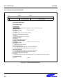
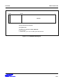
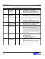
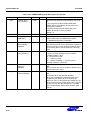
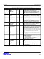
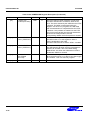
NOTES
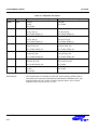
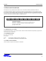
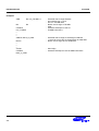
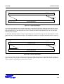
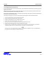
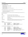
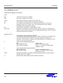
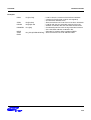
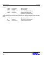
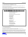
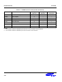
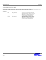
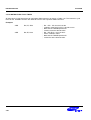
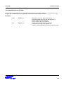
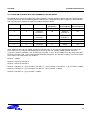
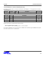
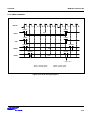
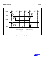
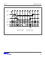
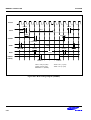
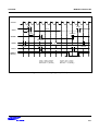
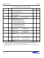
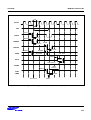
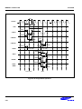
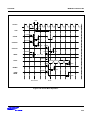
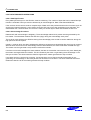
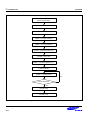
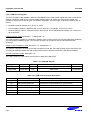
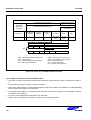
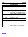
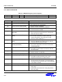
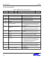
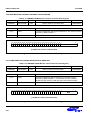
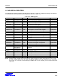
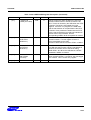
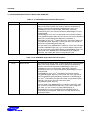
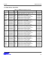
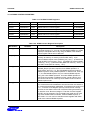
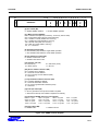
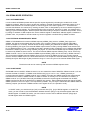
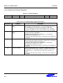
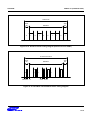
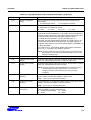
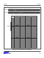
1. If WAITEN of WAITCON register is enable, memory controller can't finish access cycle until nEWAIT
signal is high. If you use slow device, you can set WAITEN to '1' and control nEWAIT signal. The
memory controller checks nEWAIT signal at the last cycle of TACC. If you set WAITEN to '0', the f
nEWAIT signal is ignored.
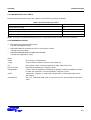
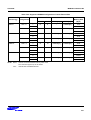
2. You can use memory control signals such as nCS, nWBE, nOE, nEWAIT for 8 bit memory, and nCS,
nWE16, nOE, nEWAIT for 16 bit memory.
3. The DW of bank 0 is the same with B0SIZE[1:0] pin. That is read only value. The initial value of
other
banks is "11".
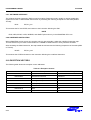
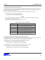
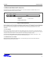
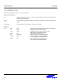
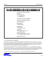
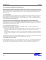
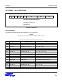
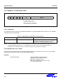
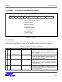
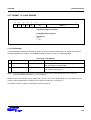
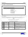
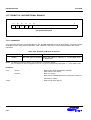
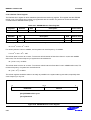
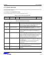
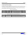
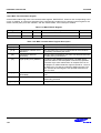
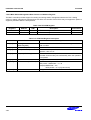
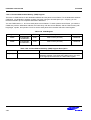
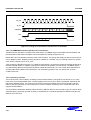
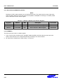
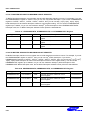
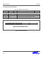
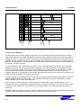
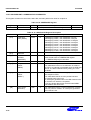
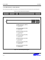
5.6.3.2 Muxed bus control register
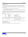
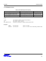
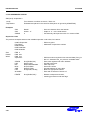
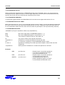
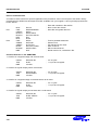
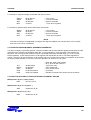
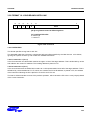
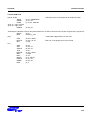
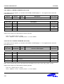
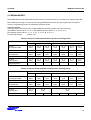
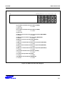
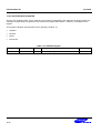
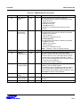
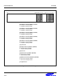
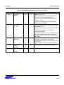
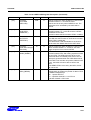
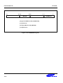
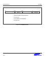
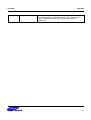
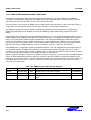
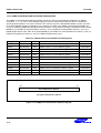
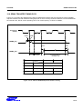
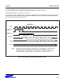
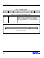
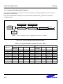
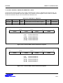
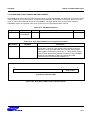
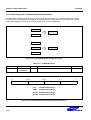
Ext I/O Bank controller supports memory devices which have the muxed bus interface. To use muxed bus
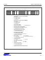
memory device, muxed bus enable(MBE) and muxed bus address cycle(TMA) for each bank in MUXBCON
register must be set.
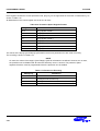
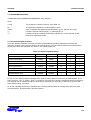
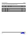
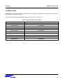
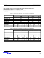
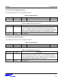
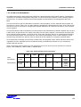
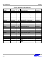
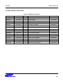
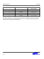
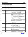
Table 5-17. Muxed Bus Control Register
Register
Address
R/W
MUXBCON
0xF0010020
R/W
Description
Muxed bus control register
Reset Value
0x006DB6DB
5-25