1
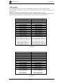
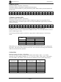
HYTEC ELECTRONICS Ltd
HEAD OFFICE: 5 CRADOCK ROAD, READING, BERKS. RG2 0JT, UK
Telephone: +44 (0) 118 9757770
Fax: +44 (0)118 9757566
E-mail: [email protected]
Copyright 2010 Hytec Electronics Ltd
Data and specifications are subject to change without notice
DAC8415
16-CHANNEL 18-BIT DAC
INDUSTRY PACK
USERS MANUAL
PCB Issue 1.0
Firmware Version 8415V102
Document Nos.: DAC8415/UTM/G/x/1.1
Date: 09/02/2012
Author: MRN
Hytec Electronics Ltd
8415/UTM/G/2/1.1
Revision History
The following table shows the revision history for this document.
Date
Version
21/10/10
09/02/12
1.0
1.1
Revision
Initial release.
Tidy up of manual.
CRITICAL APPLICATIONS DISCLAIMER
THIS PRODUCT FROM HYTEC ELECTRONICS LTD USES COMPONENTS THAT ARE NOT DESIGNED
OR INTENDED TO BE FAIL-SAFE, OR FOR USE IN ANY APPLICATION REQUIRING FAIL-SAFE
PERFORMANCE, SUCH AS IN LIFE-SUPPORT OR SAFETY DEVICES OR SYSTEMS, CLASS III MEDICAL
DEVICES, NUCLEAR FACILITIES, APPLICATIONS RELATED TO THE DEPLOYMENT OF AIRBAGS, OR
ANY OTHER APPLICATIONS THAT COULD LEAD TO DEATH, PERSONAL INJURY OR SEVERE
PROPERTY OR ENVIRONMENTAL DAMAGE (INDIVIDUALLY AND COLLECTIVELY, “CRITICAL
APPLICATIONS”).
FURTHERMORE, SOME COMPONENTS USED IN THIS HYTEC ELECTRONICS LTD PRODUCTS ARE
NOT DESIGNED OR INTENDED FOR USE IN ANY APPLICATIONS THAT AFFECT CONTROL OF A
VEHICLE OR AIRCRAFT, UNLESS THERE IS A FAIL-SAFE OR REDUNDANCY FEATURE AND A
WARNING SIGNAL UPON FAILURE TO THE OPERATOR.
THE CUSTOMER ASSUMES THE SOLE RISK AND LIABILITY OF ANY USE OF HYTEC ELECTRONICS
LTD PRODUCT IN CRITICAL APPLICATIONS.
Page 2
Hytec Electronics Ltd
8415/UTM/G/3/1.1
CONTENTS
1.
INTRODUCTION .............................................................................................................................. 4
2.
PRODUCT SPECIFICATIONS ....................................................................................................... 5
3.
OPERATING MODES ...................................................................................................................... 6
3.1
3.2
USING REGISTER TO UPDATE DACS..................................................................................... 6
USING MEMORY TO UPDATE DACS...................................................................................... 6
4.
MEMORY MAP ................................................................................................................................. 7
5.
APPLICATION REGISTERS .......................................................................................................... 8
5.1
5.2
5.3
5.4
5.5
5.6
5.7
5.8
5.9
6.
CONTROL & STATUS REGISTER (CSR) ......................................................................................... 8
MEMORY POINTER ........................................................................................................................ 9
NUMBER OF UPDATES (NOC) ....................................................................................................... 9
CLOCK RATE ................................................................................................................................. 9
INTERRUPT VECTOR .................................................................................................................... 10
EXTENDED CONTROL & STATUS REGISTER (CSR EXT) ............................................................. 10
DIGITAL POTENTIOMETER DATA REGISTER ............................................................................... 11
DAC REGISTERS ......................................................................................................................... 11
DIGITAL POTENTIOMETER CALIBRATION REGISTERS ................................................................. 11
MULTI TRIGGER AND REPEAT MULTI TRIGGER MODE ................................................ 12
6.1
6.2
MULTI TRIGGER MODE ............................................................................................................... 12
REPEAT MULTI TRIGGER MODE ................................................................................................. 12
7.
ID PROM........................................................................................................................................... 13
8.
POWER UP AND POWER DOWN AND RESET OF 8415 DAC .............................................. 14
8.1
8.2
8.3
9.
POWER UP ................................................................................................................................... 14
POWER DOWN ............................................................................................................................. 14
IP RESET ..................................................................................................................................... 14
CHANGING RANGE OF 8415 DAC ............................................................................................. 15
10.
RANGE RESOLUTION AND INSTALLATION CONSIDERATIONS................................ 16
11.
EPICS AND ASYN SOFTWARE DRIVER PLUS LINUX/WINDOWS API........................ 16
12.
SELECTION OF THE +/-12 VOLT POWER SUPPLY .......................................................... 16
APPENDIX A............................................................................................................................................ 17
APPENDIX B............................................................................................................................................ 18
APPENDIX C............................................................................................................................................ 19
APPENDIX D............................................................................................................................................ 20
Page 3
Hytec Electronics Ltd
8415/UTM/G/4/1.1
1. INTRODUCTION
The Hytec IP-DAC-8415 is a single-width Industry Pack that provides 16 channels of simultaneously
updated digital to analogue conversion with the following characteristics:• 16 independently programmed channels
• 18 bits resolution – 18 bits monotonic.
• 16 or 18 bit operation selectable by hardware or software
• On board RAM Memory 1Meg x 16 bits (64K samples for 16bits) (32K samples for 18bits).
• +/-10V full scale output range *
• +/-5V full scale output range
• 0 to 10V full scale output range
• 0 to 5V full scale output range
• Ranges software selectable
• +/- 10mA current drive capability with continuous short-circuit protection
• Drives capacitive loads to 10000pF
• Straight binary or Two Complement input code
• Internal/External update clock rates
• Internal update clock rates programmable
(50KHz,20KHz,10KHz,5KHz,2KHz,1KHz,500Hz,200Hz,100Hz,50Hz,20Hz,10Hz,5Hz,2Hz
and 1Hz)
• Maximum 64KHz external clock rate
• Simultaneous up-date Power-on disable (outputs set to 0V on boot up)
• System to plant isolation to 100V when externally powered
• Board type, Board serial number, PCB issue and firmware version held on ROM.
• External Triggering
• Continuous function generation.
• Multi Trigger Mode.
• Repeat Multi Trigger Mode.
• Field upgradeable firmware (requires Xilinx/compatible device to program built in FPGA
flash memory via the FPGA JTAG port).
* The units are factory set to have an output range of +/-10V on power up.
Page 4
Hytec Electronics Ltd
8415/UTM/G/5/1.1
2. PRODUCT SPECIFICATIONS
Size:
Single width Industry Pack 1.8ins x 3.9 ins
Operating temp:
0 to 45 deg C ambient
Number of channels: 16
DAC resolution:
18 bits
Data format +/-10V:
18 bits straight binary Code format 20h = –10v, 20000h = 0V and
3FFE0h = +10V.
Data format +/-5V:
18 bits straight binary Code format 40h = –5v, 20000h = 0V and
3FFC0h = +5V.
Data format 0-10V:
18 bits straight binary Code format 0000h = 0V and 3FFC0h = +10V.
Data format 0-5V:
18 bits straight binary Code format 0000h = 0V and 3FFC0h = +5V.
Output current:
+/-10mA @ FS
Capacitive load:
Stable up to 10000pF
Short circuit duration: Continuous
OverV withstand:
No internal protection from external voltages provided
Update rate:
64KHz max
Power quiescent:
+5V @ 350mA typical
+12V @ 150mA typical
-12V @ 100mA typical
Isolation:
100V via opto-isolators (if externally powered by HYTEC 8912)
DAC device:
Texas Instruments DAC9881SB with serial interface
Integral non-linearity: +/-1LSBs typ. +/-2LSBs max
Offset error:
+/- 32LSBs without calibration (+/-2LSBs after firmware calibration) at 25
deg C ambient. (Guaranteed for +/-10V range only).
Offset drift:
+/-0.8 ppm per deg C typical
Gain error:
+/- 32LSBs without calibration (+/-2LSBs after firmware calibration) at 25
deg C ambient. (Guaranteed for +/-10V range only).
Gain drift:
+/-10V range +/-2 ppm per deg C typical
+/-5V range +/-4 ppm per deg C typical
0-10V range 2 ppm per deg C typical
0-5V range 0.8 ppm per deg C typical
Output slew rate:
1.6V/us typ.
Page 5
Hytec Electronics Ltd
8415/UTM/G/6/1.1
3. Operating Modes
There are two operating modes:1. Registered – the DAC outputs are controlled by the contents of the DAC registers.
2. Memory – the DAC outputs are updated for the programmed number of samples at the programmed
clock rate from the RAM memory.
All the outputs are updated serially but change together (there will be slight changes due to differences in
the slew rate of the amplifiers (about +/-1uS) at the end of an internal update cycle.
The outputs may be updated at a rate of up to 64KHz. The two methods to update the 8415 DACs are
detailed below.
3.1 USING REGISTER TO UPDATE DACs
For this mode set EX=’0’ and ARM=’1’ in the CSR.
In 18bit mode there are two registers per DAC channel giving a torla of 32 registers. These can be loaded
one at a time, the module can then be ARMed and the data from the registers will be serially loaded from
one DAC to the next until all the data has been passed to the DACs. At this point the DAC outputs are
automatically updated giving 16 simultaneous outputs. Then ARM bit is cleared.
In this mode the output sample clock is not used as the output is set when ARM is set.
All the outputs change together.
3.2 USING MEMORY TO UPDATE DACs
To select this mode set the following bits:-EX=’1’, ARM=’1’ in the CSR. Trigger using software trigger
(ST) or external hardware trigger.
In this method the memory is first loaded with the required data and the number of memory locations
used is entered in to the Number of Updates (NOC) register. The Control and Status Register (CSR) is
then set to enable memory updates and ARM to unit with a software command. A trigger can then be
issued either by a software command or by an external trigger to start down loading the data held in
memory to the DACs via the registers as detail above. In this mode the registers are updated with new
data from the memory at the update clock rate which is derived either internally or externally. The
memory address is automatically incremented.
The unit can be programmed to generate an interrupt when memory is Half Full, Full or when the
programmed number of outputs has occurred.
When the programmed number of output has occurred the unit will stop and ARM will be cleared.
In continuous mode, when the programmed number of output has occurred, the address counter will be
zeroed and the output repeated until the ARM bit is cleared or the Cont bit in the CSR is cleared (no
interrupt generated in continues mode). If the Cont bit is cleared, the unit will stop when the
programmed number of output (NOC) has been reached.
The following should be loaded in to the NOC to output whole or half the memory in the following
modes.
Memory Size
(1MB in CSR)
2Mb
2Mb
1Mb
1Mb
Mode
18 Bit
16 Bit
18 Bit
16 Bit
NOC Values
Half memory
Full Memory
0x4000
0x8000
0x8000
0x0
0x2000
0x4000
0x4000
0x8000
When 1Mb is set the only change is when the Full and Half Full memory flags and interrupts occur as
shown in the above table. The user must ensure that the correct NOC value is entered as the setting of
the 1Mb in the CSR does not effect the NOC operation.
Page 6
Hytec Electronics Ltd
8415/UTM/G/7/1.1
4. Memory Map
On board RAM Memory is 1M x 16 bits (64K samples per channel for 16bits) (32K for 18bits).
When used in the sixteen bit mode, there are two main buffer memories of 512k updates each (lower and
upper buffers).
These are each divided into sixteen segments allocated to updates for DAC1 to DAC16.
When DAC16 has been updated from the top of the lower buffer, the Half memory Flag status is set and
when it has been updated from the top of the upper memory buffer the Full Flag status is set.
Lower Conversion Memory
Upper Conversion Memory
DAC16 conversions
DAC15 conversions
DAC14 conversions
DAC13 conversions
DAC12 conversions
DAC11 conversions
DAC10 conversions
DAC9 conversions
DAC8 conversions
DAC7 conversions
DAC6 conversions
DAC5 conversions
DAC4 conversions
DAC3 conversions
DAC2 conversions
DAC1 conversion 16k (bits16 - 17)
DAC1 conversion 16k (bits 0 -15)
DAC1 conversion 16k-1 (bits16 - 17)
DAC1 conversion 16k-1 (bits 0 -15)
DAC16 conversions
DAC15 conversions
DAC14 conversions
DAC13 conversions
DAC12 conversions
DAC11 conversions
DAC10 conversions
DAC9 conversions
DAC8 conversions
DAC7 conversions
DAC6 conversions
DAC5 conversions
DAC4 conversions
DAC3 conversions
DAC2 conversions
DAC1 conversion 32k (bits16 - 17)
DAC1 conversion 32k (bits 0 -15)
DAC1 conversion 32k-1 (bits16 - 17)
DAC1 conversion 32k-1 (bits 0 -15)
DAC1 conversion 2 (bits16 - 17)
DAC1 conversion 2 (bits 0 -15)
DAC1 conversion 1 (bits16 - 17)
DAC1 conversion 1 (bits 0 -15)
DAC1 conversion 16k+2 (bits16 - 17)
DAC1 conversion 16k+2 (bits 0 -15)
DAC1 conversion 16k+1 (bits16 - 17)
DAC1 conversion 16k+1 (bits 0 -15)
18 Bit Mode
Lower Conversion Memory
Upper Conversion Memory
DAC16 conversions
DAC15 conversions
DAC14 conversions
DAC13 conversions
DAC12 conversions
DAC11 conversions
DAC10 conversions
DAC9 conversions
DAC8 conversions
DAC7 conversions
DAC6 conversions
DAC5 conversions
DAC4 conversions
DAC3 conversions
DAC2 conversions
DAC1 conversion 32k
DAC1 conversion 32k-1
DAC16 conversions
DAC15 conversions
DAC14 conversions
DAC13 conversions
DAC12 conversions
DAC11 conversions
DAC10 conversions
DAC9 conversions
DAC8 conversions
DAC7 conversions
DAC6 conversions
DAC5 conversions
DAC4 conversions
DAC3 conversions
DAC2 conversions
DAC1 conversion 64k
DAC1 conversion 64k-1
DAC1 conversion 2
DAC1 conversion 1
DAC1 conversion 32k+2
DAC1 conversion 32k+1
16 Bit Mode
Page 7
Hytec Electronics Ltd
8415/UTM/G/8/1.1
5. Application Registers
5.1 Control & Status Register (CSR)
Read/Write Address: Byte 0hex (Word 0hex)
D15 D14 D13 D12 D11 D10 D09 D08 D07 D06 D05 D04 D03 D02 D01 D00
ARM EX ST XC ET EE FE HE BS SSU 1MB MH CONT CC
F
HF
ARM Writing a ‘1’ to ARM bit causes the values loaded in to the DAC registers or the memory
to be loaded in to the DACs.
When all the DACs have been updated from the registers (the EX bit set to ‘0’) the ARM
bit is cleared.
If the DACs are being updated from the memory (the EX bit set to ‘1’) the ARM bit is not
cleared.
In this mode if a number of triggers occur which cause the end of the memory to be
reached, a subsequent trigger will cause the memory pointer to wrap around to the start
of memory.
EX
Enable trigger and memory update.
EX=0 The outputs will be loaded from the DAC registers.
EX=1 Allows external trigger or software trigger to initiate programmed updates from
memory. In this mode the Number Of Updates Register (NOC) needs to be set between
0 to 64K updates.
ST
Software trigger. Triggers the programmed number of updates from the memory as set
by the Number of Updates register.
XC
Enable the external clock. 0 = internal clock used for the sample rate. 1 = external clock
used for the sample rate.
ET
When set to ‘1’ enables Inhibiting via the Lemo of the 8002 via the IP Strobe line. The
Inhibit signal when set stops updating the DAC from memory.
EE
Enables interrupt at end of programmed number of DAC updates from memory.
FE
Enables interrupt when the upper conversion memory has been filled. (Memory Full).
HE
Enables interrupt when the lower conversion memory has been filled. (Memory Half
Full).
BS
Busy status: Flag showing unit is busy shifting data to DAC’s or in process of changing
range.
SSU
Writing a ‘1’ will set all DAC outputs to zero (this bit is auto cleared on completion)
1MB
Enable 1Mb memory (32K values/channel) when logic 1 and 2Mb (64K values/channel)
when logic 0.
MH
Set to ‘1’ when the memory is inhibited from the IP Strobe line and ET is set.
CONT Sets continuous function generation
CC
Conversions complete. Status bit set when the number of programmed updates has
been completed. Generates IRQ0* if set and EE is set to a logic 1.
F
Full status. Set when DAC16 has been updated from the top of memory. Generates
IRQ0* if set and FE is set to a logic 1.
HF
Half full status. Set when DAC16 has been updated from the top of the lower memory
buffer. Generates IRQ0* if set and HE is set to a logic 1.
Page 8
Hytec Electronics Ltd
8415/UTM/G/9/1.1
5.2 Memory Pointer
Read/write Address: Byte 2hex (Word 1hex)
The Memory pointer is the number of updates held in the memory.
The current conversion address is given by the Memory pointer address offset by the DAC number and
the Full status.
D15 D14 D13 D12 D11 D10 D09 D08 D07 D06 D05 D04 D03 D02 D01 D00
C15 C14 C13 C12 C11 C10 C9 C8 C7 C6 C5 C4 C3 C2 C1 C0
5.3 Number of updates (NOC)
Read/write Address: Byte 4hex (Word 2hex)
The number of updates register allows the number of updates per trigger to be programmed. If the
memory buffer size is exceeded the update values will wrap around from the upper memory to the base
of the lower memory.
D15 D14 D13 D12 D11 D10 D09 D08 D07 D06 D05 D04 D03 D02 D01 D00
N15 N14 N13 N12 N11 N10 N9 N8 N7 N6 N5 N4 N3 N2 N1 N0
If the CONT bit =’1’ set in CSR then the set number of outputs is output continuously.
If CONT not set then set nos bit output then the TRIGEN is cleared. CC in the CSR needs to be cleared
before a further trigger is seen.
The following should be loaded in to the NOC to output whole or half the memory in the following
modes.
Mode
18 Bit 2Mb
16 Bit 2Mb
18 Bit 1Mb
16 Bit 1Mb
NOC Values
Half Full
0x4000
0x8000
0x2000
0x4000
Full
0x8000
0x0
0x4000
0x8000
When 1Mb is set it only changes when the Full and Half Full flags and interrupts occur as shown in the
above table. The user must ensure that the correct NOC value is entered as the setting of the 1Mb in the
CSR does not effect the NOC operation.
5.4 Clock Rate
Read/write Address: Byte 6hex (Word 3hex)
The clock rate register is a four bit register (D00 to D03) which enables codes 0 – 13 to enable
frequencies of 1 Hz to 50kHz in multiples of 1, 2, 5 or 10. (E.g. 0=1Hz, 1=2Hz, 2=5Hz, 3=10Hz and so
on to 0xD=20KHz , 0xE=50KHz). Each clock pulse will initiate all 16 DAC updates from memory.
Clock rate Reg
(D3 to D0)
0000
0001
0010
0011
0100
0101
0110
0111
Frequency
Hz
1
2
5
10
20
50
100
200
Clock rate Reg
(D3 to D0)
1000
1001
1010
1011
1100
1101
1110
1111
Page 9
Frequency
Hz
500
1MHz
2MHz
5MHz
10MHz
20MHz
50MHz
-
Hytec Electronics Ltd
8415/UTM/G/10/1.1
5.5 Interrupt Vector
Read/write Address: Byte 8hex (Word 4hex)
The vector register is a 16 bit register which stores the interrupt vector value.
D15
V15
D14
V14
D13
V13
D12
V12
D11
V11
D10
V10
D09
V9
D08
V8
D07
V7
D06
V6
D05
V5
D04
V4
D03
V3
D02
V2
D01
V1
D00
V0
5.6 Extended Control & Status Register (CSR Ext)
Read/write Address: Byte Ahex (Word 5hex)
This gives added functionality over the 8402
D15 D14
EN16 CAL
D13
D12
D11
D10
E
D09 D08
EFW IFW
D07
D06
D05
RP
D04
MT
D03
D02
BTC
D01
R1
D00
R0
R
This sets range from "00"=+/-10V, "01"+/-5V, "10"=0-10V & "11"=0-5V.
BTC
‘0’= DAC input data straight binary ‘1’= DAC input data twos complement.
MT
Multi trigger mode.
RP
Cycle memory in Multi trigger mode
IFW
Do not set this bit as setup and calibration data maybe lost. This bit enables the
FPGA flash write from buffer command
EFW
Do not set this bit as setup and calibration data maybe lost. This bit enables the
External flash write by writing to IP mem i.e. switches off RAM
E
Do not set this bit as setup and calibration data maybe lost. This bit enables the
External flash chip or sector erase when do a IP write to mem. If IP data is 0x10 then
chip erase (64s time taken) if IP data is 0x30 then sector erase where the sector
address is given in the IP memory address lines. If chip erase then IP mem address =
0x555 and data 0x10.
CAL
If set to '1' unit does not use on board flash calibration for register updates only. If
EX=1 then this has no effect. Used for production test.
EN16
If set to '1' makes the unit same as the Hytec 8402 16 bit DAC. This bit can also be set
by jumper J3 on PCB.
Page 10
Hytec Electronics Ltd
8415/UTM/G/11/1.1
5.7 Digital Potentiometer Data Register
Read/write Address: Byte Chex (Word 6hex)
This is used for calibration only during production test on the units.
D15 D14 D13 D12 D11 D10 D09 D08 D07 D06 D05 D04 D03 D02 D01 D00
EN PD CWR X
X
X
P9
P8
P7
P6
P5
P4
P3
P2
P1
P0
The ‘EN’ (bit 15) when set as a ‘1’ will cause the current value of the register to be down loaded to the
10bit digital pot. On completion of the write the EN bit is cleared. The rest of the contents of the
register remain unaltered.
PD bit when set to ‘1’ loads the digital pot range data held in FPGA flash to registers in the FPGA. This
is for production use only.
CWR bit copies wiper register in in digital pot to the non-volatile register in digital pot. This is for
production use only.
The user can use this register to tweak the gain error of the unit if required. This maybe be used to
compensate for ambient temperature.
5.8 DAC Registers
Read/write Address: Byte 10hex – 4Ehex (Word 8hex – 27hex)
The 16 DACs are updated from these registers when ARM is set EX bit is zero. On completion the ARM
bit is cleared.
Straight binary data format or Twos Complement Code set by BTC bit of CSR Ext register.
16 bit code (as Hytec 8402) this uses address 10hex to 2Ehex (Word 8hex – 17hex) for channels 1
to 16.
D15
C17
D14
C16
D13
C15
D12
C14
D11
C13
D10
C12
D09
C11
D08
C10
D07
C9
D06
C8
D05
C7
D04
C6
D03
C5
D02
C4
D01
C3
D00
C2
D05
C5
D04
C4
D03
C3
D02
C2
D01
C1
D00
C0
D05
0
D04
0
D03
0
D02
0
D01
C17
D00
C16
18 bit code this uses address 10hex to 4Ehex (Word 8hex – 27hex)
i.e. channel 1 address of low word is 10hex (Word 8hex)
D15
C15
D14
C14
D13
C13
D12
C12
D11
C11
D10
C10
D09
C9
i.e. channel 1 address of high word is 12hex
D15
0
D14
0
D13
0
D12
0
D11
0
D10
0
D09
0
D08
C8
D07
C7
D06
C6
(Word 9hex)
D08
0
D07
0
D06
0
5.9 Digital Potentiometer Calibration Registers
Read Address: Byte 60hex – 66hex (Word 30hex – 33hex)
D15 D14 D13 D12 D11 D10 D09 D08 D07 D06 D05 D04 D03 D02 D01 D00
X
X
X
X
X
X
P9
P8
P7
P6
P5
P4
P3
P2
P1
P0
These four registers hold the digital pot calibration factor for each of the DACs voltage ranges. The
values are loaded at power up from the FPGA flash or when ‘PD’ (bit 14) of the digital pot register is set
to ‘1’ this is cleared at the finish.
When the range is changed the data held in the associated register is loaded to the digital potentiometer.
The calibration values held in the FPGA flash are programmed in during production test.
The digital pot can still be changed using the Digital Potentiometer Register above but the digital pot will
reload its self from the calibration registers on power up and on a range change.
Page 11
Hytec Electronics Ltd
8415/UTM/G/12/1.1
6. MULTI TRIGGER AND REPEAT MULTI TRIGGER MODE
Multi trigger mode is set by bit 4 (MT) in the Ext CSR. This allows the user to repeatedly trigger the
unit. The number of updates is set by the NOC register. When the unit is triggered and the required
number of updates output the CC flag in the CSR is set and the unit stopped.
6.1 Multi Trigger Mode
In this mode the memory address pointer is not cleared. On the subsequent triggers the CC flag is
cleared then at the end of the number of update is reset. If the half full or full points of the memory are
reached then the half Full and Full Flags will be set. If memory reaches full it will wrap a round and
repeat either with the next trigger or if number of updates take it over the memory full then it will wrap.
Also the memory Half Full and Full flags will NOT be cleared once set.
D
A
C
Multi Trigger Mode
CM=1 RP=0
O
u
t
p
u
t
f
r
o
m
M
e
m
o
r
y
T1
T2
T3
T4
6.2 Repeat Multi Trigger Mode
Repeat multi trigger mode is set by bit 5 (RP) in Ext CSR. In repeat multi trigger mode the address
pointer is cleared on each trigger.
D
A
C
Repeat Multi Trigger Mode
CM=1 RP=1
O
u
t
p
u
t
f
r
o
m
M
e
m
o
r
y
T1
T2
T3
T4
Page 12
Hytec Electronics Ltd
8415/UTM/G/13/1.1
7. ID PROM
The ID data is stored in Flash memory. The word addresses are as below:Base+80
Base+82
Base+84
Base+86
Base+88
Base+8A
Base+8C
Base+8E
Base+90
Base+92
Base+94
Base+96
Base+98
Base+9A
Base+9C
Base+9E
ASCII ‘VI’
ASCII ‘TA’
ASCII ‘4 ‘
Hytec ID high byte
Hytec ID low word
Model number
Revision
Reserved
Driver ID
Driver ID
Flags
No of bytes used
Cal Type
Serial Number
Not used
Not used
5649h
5441h
3420h
0080h
0300h
8415h
1102h This shows PCB Iss 1 and FPGA firmware at Ver 102
0000h
0000h
0000h
0006h This shows 8MHz and 32MHz operation
001Ah
0000h 0 = No Calibration factors.
xxxxdec
0000h
0000h
Page 13
Hytec Electronics Ltd
8415/UTM/G/14/1.1
8. POWER UP AND POWER DOWN AND RESET OF 8415 DAC
8.1 Power Up
During power up the 8415 outputs should remain approx zero volts with transients as shown below
8.2 Power Down
At power down the 8415 outputs are not guaranteed to remain steady.
8.3 IP Reset
An IP reset will set the DAC output voltage to zero and set the range to +/-10V.
Reset clears the following registers:CSR.
NOC.
All DAC registers are zeroed.
Page 14
Hytec Electronics Ltd
8415/UTM/G/15/1.1
9. CHANGING RANGE OF 8415 DAC
The DAC 8415 powers on in the +/-10V range. When the range is change by writing to bits 0 and 1 of
the ExtCSR the DAC will be offline for approx 20mS. During this time the DAC output will be zeroed
and the new reference and offset voltages applied. During this process the output may glitch as shown in
the following scope shots.
Two glitches can occur as shown in the scope shot below.
First glitch will be negative 2.5V if going to +/-10V range or negative 5V if going to +/-5V.
The second glitch will be +5V if going to +/-10V range or +2.5V if going from to +/-5V
Page 15
Hytec Electronics Ltd
8415/UTM/G/16/1.1
When going from +/-5V to 0-10V then only first glitch to 2.5V.
When going from 0-10V to +/-5V only second glitch at 2.5V.
When going from +/-10V to 0-5V then only first glitch to 5V.
When going from 0-5V to +/-10V only second glitch at 5V.
When going from +/-10V to 0-10V then only first glitch to 5V.
When going from 0-10V to +/-10V only first glitch at 5V.
When going from +/-5V to 0-5V then only first glitch to 2.5V.
When going from 0-5V to +/-5V only first glitch at 2.5V.
When going between 0-5V and 0-10V no glitches occur
10.RANGE RESOLUTION AND INSTALLATION CONSIDERATIONS
The following table shows the resolution per range:
Range
+/-10V
+/-5V
+10V
+5V
Resolution
76.312576uV
38.165608uV
38.156288uV
19.078144uV
Due to the high resolution and linearity of the DAC, system design problems such as grounding and
contact resistance become very important. For this 18bit converter with a 20V full-scale range , 1LSB is
76.312576uV. With a load current of 5mA, series wiring and connector resistance of only 60mohms will
cause an output error of 2LSBs.
To put this in contexts the resistance of #23 wire is about 0.067ohms/meter. Neglecting contact
resistance, less than 1 meter of wire will produce an error greater than 2LSBs in the analogue output
voltage.
11.EPICS and ASYN Software Driver Plus Linux/Windows API
EPICS and ASYN software drivers are in avalable for the DAC8415 16 channel DAC Industry Pack.
For downloads go to:
www.hytec-electronics.co.uk/Download.aspx
A Linux/Windowa API is available, consult Hytec for details.
12.SELECTION OF THE +/-12 VOLT POWER SUPPLY
The DAC 8415 +/-12 volt power supply can be derived either internally from the carrier card or from an
external source via a transition card. The source is selected using jumpers J1, J2 and the GND AGND
link LNK1 where:
J1 External +12V connect 1 & 2, Internal +12V connect 2 & 3
J2 External -12V connect 1 & 2, Internal -12V connect 2 & 3
LNK1 (GND AGND)
IN for internal +/-12V
OUT for external +/-12V (supplied from transition card DC DC converter).
Page 16
Hytec Electronics Ltd
8415/UTM/G/17/1.1
APPENDIX A
PCB JUMPERS
Issue 1 PCB
J1 External +12V connect 1 & 2, Internal +12V connect 2 & 3
J2 External -12V connect 1 & 2, Internal -12V connect 2 & 3
J3 Sets 16bit mode when IN This overrides the EN16 bit in the CSR Ext(Factory set OUT)
J4 Not used. Jumper for J3 located here for shipment.
LNK1 Factory set IN links VME GND and AGND
Page 17
Hytec Electronics Ltd
8415/UTM/G/18/1.1
APPENDIX B
I/O Connector – PL2 (50 way) on 8415 DAC PCB
Pin
1
2
3
4
5
6
7
8
9
10
11
12
13
14
15
16
17
18
19
20
21
22
23
24
25
Signal
Output 1
AGND
Output 2
AGND
Output 3
AGND
Output 4
AGND
Output 5
AGND
Output 6
AGND
Output 7
AGND
Output 8
AGND
Output9
AGND
Output10
AGND
Output11
AGND
Output12
AGND
Output13
Pin
26
27
28
29
30
31
32
33
34
35
36
37
38
39
40
41
42
43
44
45
46
47
48
49
50
Page 18
Signal
AGND
Output14
AGND
Output15
AGND
Output16
AGND
N.C.
N.C.
XTrigger
/XTrigger
N.C.
N.C.
XClk
/XClk
+12VX
AGND
+12VX
AGND
-12VX
AGND
-12VX
AGND
N.C.
AGND
Hytec Electronics Ltd
8415/UTM/G/19/1.1
APPENDIX C
HYTEC TRANSITION CARD 8202 CONNECTIONS
I/O Connector – 50 way on transition panel
Pin
1
2
3
4
5
6
7
8
9
10
11
12
13
14
15
16
17
18
19
20
21
22
23
24
25
Signal
AGND
AGND
AGND
AGND
AGND
AGND
AGND
AGND
AGND
AGND
AGND
AGND
AGND
AGND
AGND
AGND
Pin
26
27
28
29
30
31
32
33
34
35
36
37
38
39
40
41
42
43
44
45
46
47
48
49
50
XTRIG N
XCLK N
AGND
AGND
Page 19
Signal
Output1
Output 2
Output 3
Output 4
Output 5
Output 6
Output 7
Output 8
Output 9
Output 10
Output 11
Output 12
Output 13
Output 14
Output 15
Output 16
XTRIG P
XCLK P
AGND
AGND
Hytec Electronics Ltd
8415/UTM/G/20/1.1
APPENDIX D
VME64X PIN ASSIGNMENT ON HYTEC 8002/4 IP CARRIER BOARD FOR DAC8415
ROW A
P0.A01
P0.A02
P0.A03
P0.A04
P0.A05
P0.A06
P0.A07
P0.A08
P0.A09
P0.A10
P0.A11
P0.A12
P0.A13
P0.A14
P0.A15
P0.A16
P0.A17
P0.A18
P0.A19
SIG
D Chan 1+
D Chan 3 D Chan 6+
D Chan 8 D Chan 11+
D Chan 13 D Chan 16+
D/XTrigger
D +12V
D AGND
C Chan 1+
C Chan 3 C Chan 6+
C Chan 8C Chan 11+
C Chan 13C Chan 16+
C/XTrigger
C +12V
ROW B
P0.B01
P0.B02
P0.B03
P0.B04
P0.B05
P0.B06
P0.B07
P0.B08
P0.B09
P0.B10
P0 B11
P0.B12
P0.B13
P0.B14
P0.B15
P0.B16
P0.B17
P0.B18
P0.B19
SIG
D Chan 1D Chan 4+
D Chan 6 D Chan 9+
D Chan 11 D Chan 14 +
D Chan 16 N/C
D AGND
D -12V
C Chan 1 C Chan 4+
C Chan 6C Chan 9+
C Chan 11C Chan 14+
C Chan 16N/C
C AGND
ROW C
P0.C01
P0.C02
P0.C03
P0.C04
P0.C05
P0.C06
P0.C07
P0.C08
P0.C09
P0.C10
P0.C11
P0.C12
P0.C13
P0.C14
P0.C15
P0.C16
P0.C17
P0.C18
P0.C19
SIG
D Chan 2+
D Chan 4 D Chan 7+
D Chan 9 D Chan 12 +
D Chan 14 N/C
N/C
D +12V
D AGND
C Chan 2+
C Chan 4 C Chan 7+
C Chan 9C Chan 12+
C Chan 14N/C
N/C
C +12V
ROW D
P0.DO1
P0.D02
P0.D03
P0.D04
P0.D05
P0.D06
P0.D07
P0.D08
P0.D09
P0.D10
P0.D11
P0.D12
P0.D13
P0.D14
P0.D15
P0.D16
P0.D17
P0.D18
P0.D19
SIG
D Chan 2 D Chan 5+
D Chan 7 D Chan 10 +
D Chan 12 D Chan 15 +
N/C
D XCLK
D AGND
N/C
C Chan 2 C Chan 5+
C Chan 7 C Chan 10+
C Chan 12C Chan 15+
N/C
C XCLK
C AGND
ROW E
P0.E01
P0.E02
P0.E03
P0.E04
P0.E05
P0.E06
P0.E07
P0.E08
P0.E09
P0.E10
P0 E11
P0.E12
P0.E13
P0.E14
P0.E15
P0.E16
P0.E17
P0.E18
P0.E19
SIG
D Chan 3+
D Chan 5 D Chan 8+
D Chan 10 D Chan 13 +
D Chan 15 D XTrigger
D /XCLK
D -12V
D AGND
C Chan 3+
C Chan 5 C Chan 8+
C Chan 11+
C Chan 13+
C Chan 15C XTrigger
C /XCLK
C -12V
ROW F
P0.F01
P0.F02
P0.F03
P0.F04
P0.F05
P0.F06
P0.F07
P0.F08
P0.F09
P0.F10
P0.F11
P0.F12
P0.F13
P0.F14
P0.F15
P0.F16
P0.F17
P0.F18
P0.F19
SIG
GND
GND
GND
GND
GND
GND
GND
GND
GND
GND
GND
GND
GND
GND
GND
GND
GND
GND
GND
P0 pin assignment
P1 ROW A
P1.A01
P1.A02
P1.A03
P1.A04
P1.A05
P1.A06
P1.A07
P1.A08
P1.A09
P1.A10
P1.A11
P1.A12
P1.A13
P1.A14
P1.A15
P1.A16
P1.A17
P1.A18
P1.A19
P1.A20
P1.A21
P1.A22
P1.A23
P1.A24
P1.A25
P1.A26
P1.A27
P1.A28
P1.A29
P1.A30
P1.A31
P1.A32
SIGNAL
D00
D01
D02
D03
D04
D05
D06
D07
GND
N/C
GND
DS1*
DS0*
WRITE
GND
DTACK*
GND
AS
GND
IACK
IACKIN*
IACKOUT
AM4
A07
A06
A05
A04
A03
A02
A0l
-12V
+5V
P1 ROW B
P1.B01
P1.B02
P1.B03
P1.B04
P1.B05
P1.B06
P1.B07
P1.B08
P1.B09
P1.B10
P1.B11
P1.B12
P1.B13
P1.B14
P1.B15
P1.B16
P1.B17
P1.B18
P1.B19
P1.B20
P1.B21
P1.B22
P1.B23
P1.B24
P1.B25
P1.B26
P1.B27
P1.B28
P1.B29
P1.B30
P1.B31
P1.B32
SIGNAL
N/C
N/C
N/C
BG0IN*
BG0OUT*
BG1IN*
BG1OUT*
BG2IN*
BG2OUT*
BG3IN*
BG3OUT*
N/C
N/C
N/C
N/C
AM0
AM1
AM2
AM3
GND
N/C
N/C
GND
IRQ7*
IRQ6*
IRQ5*
IRQ4*
IRQ3*
IRQ2*
IRQ1*
N/C
+5V
P1 ROW C
P1.C01
P1.C02
P1.C03
P1.C04
P1.C05
P1.C06
P1.C07
P1.C08
P1.C09
P1.C10
P1.C11
P1.C12
P1.C13
P1.C14
P1.C15
P1.C16
P1.C17
P1.C18
P1.C19
P1.C20
P1.C21
P1.C22
P1.C23
P1.C24
P1.C25
P1.C26
P1.C27
P1.C28
P1.C29
P1.C30
P1.C31
P1.C32
SIGNAL
D08
D09
D10
D11
D12
D13
D14
D15
GND
N/C
BERR*
RESET
LWORD*
AM5
A23
A22
A21
A20
A19
A18
A17
A16
A15
A14
A13
A12
A11
A10
A09
A08
+12V
+5V
P1 Pin Assignment
Page 20
P1 ROW D
P1.D01
P1.D02
P1.D03
P1.D04
P1.D05
P1.D06
P1.D07
P1.D08
P1.D09
P1.D10
P1.D11
P1.D12
P1.D13
P1.D14
P1.D15
P1.D16
P1.D17
P1.D18
P1.D19
P1.D20
P1.D21
P1.D22
P1.D23
P1.D24
P1.D25
P1.D26
P1.D27
P1.D28
P1.D29
P1.D30
P1.D31
P1.D32
SIGNAL
N/C
N/C
N/C
N/C
N/C
N/C
N/C
N/C
N/C
N/C
N/C
+3.3V
N/C
+3.3V
N/C
+3.3V
N/C
+3.3V
N/C
+3.3V
N/C
+3.3V
N/C
+3.3V
N/C
+3.3V
N/C
+3.3V
N/C
+3.3V
N/C
+5V
P1 ROW Z
P1.Z01
P1.Z02
P1.Z03
P1.Z04
P1.Z05
P1.Z06
P1.Z07
P1.Z08
P1.Z09
P1.Z10
P1.Z11
P1.Z12
P1.Z13
P1.Z14
P1.Z15
P1.Z16
P1.Z17
P1.Z18
P1.Z19
P1.Z20
P1.Z21
P1.Z22
P1.Z23
P1.Z24
P1.Z25
P1.Z26
P1.Z27
P1.Z28
P1.Z29
P1.Z30
P1.Z31
P1.Z32
SIGNAL
N/C
GND
N/C
GND
N/C
GND
N/C
GND
N/C
GND
N/C
GND
N/C
GND
N/C
GND
N/C
GND
N/C
GND
N/C
GND
N/C
GND
N/C
GND
N/C
GND
N/C
GND
N/C
GND
Hytec Electronics Ltd
ROWA
P2.A01
P2.A02
P2.A03
P2.A04
P2.A05
P2.A06
P2.A07
P2.A08
P2.A09
P2.A10
P2.A11
P2.A12
P2.A13
P2.A14
P2.A15
P2.A16
P2.A17
P2.A18
P2.A19
P2.A20
P2.A21
P2.A22
P2.A23
P2.A24
P2.A25
P2.A26
P2.A27
P2.A28
P2.A29
P2.A30
P2.A31
P2.A32
SIG
+12V
+12V
-12V
-12V
N/C
A Chan 1 +
A Chan 2 +
A Chan 3 +
A Chan 4 +
A Chan 5 +
A Chan 6 +
A Chan 7 +
A Chan 8 +
A Chan 9 +
A Chan 10 +
A Chan 11 +
A Chan 12 +
A Chan 13 +
A Chan 14 +
A Chan 15 +
A Chan 16 +
N/C
A X Trigger
N/C
A XCLK
A +12V
A +12V
A -12V
A -12V
N/C
Out+3.3V
Out +5V
B
B
B
B
ROWB
P2.B01
P2.B02
P2.B03
P2.B04
P2.B05
P2.B06
P2.B07
P2.B08
P2.B09
P2.B10
P2.B11
P2.B12
P2.B13
P2.B14
P2.B15
P2.B16
P2.B17
P2.B18
P2.B19
P2.B20
P2.B21
P2.B22
P2.B23
P2.B24
P2.B25
P2.B26
P2.B27
P2.B28
P2.B29
P2.B30
P2.B31
P2.B32
8415/UTM/G/21/1.1
SIG
+5V
GND
N/C
A24
A25
A26
A27
A28
A29
A30
A31
GND
+5V
N/C
N/C
N/C
N/C
N/C
N/C
N/C
N/C
GND
N/C
N/C
N/C
N/C
N/C
N/C
N/C
N/C
GND
+5V
ROWC
P2.C01
P2.C02
P2.C03
P2.C04
P2.C05
P2.C06
P2.C07
P2.C08
P2.C09
P2.C10
P2.C11
P2.C12
P2.C13
P2.C14
P2.C15
P2.C16
P2.C17
P2.C18
P2.C19
P2.C20
P2.C21
P2.C22
P2.C23
P2.C24
P2.C25
P2.C26
P2.C27
P2.C28
P2.C29
P2.C30
P2.C31
P2.C32
SIG
B AGND
B AGND
B AGND
B AGND
B AGND
A Chan 1 A Chan 2 A Chan 3 A Chan 4 A Chan 5 A Chan 6 A Chan 7 A Chan 8 A Chan 9 A Chan 10 A Chan 11 A Chan 12 A Chan 13 A Chan 14 A Chan 15 A Chan 16 N/C
A /XTrigger
N/C
A /XCLK
A AGND
A AGND
A AGND
A AGND
A AGND
Out+3.3V
Out +5V
ROWD
P2.D01
P2.D02
P2.D03
P2.D04
P2.D05
P2.D06
P2.D07
P2.D08
P2.D09
P2.D10
P2.D11
P2.D12
P2.D13
P2.D14
P2.D15
P2.D16
P2.D17
P2.D18
P2.D19
P2.D20
P2.D21
P2.D22
P2.D23
P2.D24
P2.D25
P2.D26
P2.D27
P2.D28
P2.D29
P2.D30
P2.D31
P2.D32
SIG
C -12V
C AGND
C AGND
B Chan 1 +
B Chan 2 +
B Chan 2 B Chan 3 B Chan 4 +
B Chan 5 +
B Chan 5 B Chan 6 B Chan 7 +
B Chan 8 +
B Chan 8 B Chan 9 B Chan 10 +
B Chan 11 +
B Chan 11 B Chan 12 B Chan 13 +
B Chan 14 +
B Chan 14 B Chan 15 B Chan 16 +
N/C
N/C
B /XTrigger
N/C
B XCLK
B /XCLK
GND
PC +5V
P2 pin assignment
Denotes pins with thickened tracks which can be used for power inputs
Page 21
ROWZ
P2.Z01
P2.Z02
P2.Z03
P2.Z04
P2.Z05
P2.Z06
P2.Z07
P2.Z08
P2.Z09
P2.Z10
P2.Z11
P2.Z12
P2.Z13
P2.Z14
P2.Z15
P2.Z16
P2.Z17
P2.Z18
P2.Z19
P2.Z20
P2.Z21
P2.Z22
P2.Z23
P2.Z24
P2.Z25
P2.Z26
P2.Z27
P2.Z28
P2.Z29
P2.Z30
P2.Z31
P2.Z32
SIG
C AGND
GND
N/C
GND
B Chan 1 GND
B Chan 3 +
GND
B Chan 4 GND
B Chan 6 +
GND
B Chan 7 GND
B Chan 9 +
GND
B Chan 10 GND
B Chan 12+
GND
B Chan 13 GND
B Chan 15+
GND
B Chan 16 GND
B X Trigger
GND
N/C
GND
Out +3.3V
GND