1
Application Notes 9821
Functional Description
Voltage Reference
The HI5760 has an internal 1.2V voltage reference with a
±60ppm/oC drift coefficient over the full temperature range
of the converter. The REFLO pin (16) selects the reference.
Access to pin 16 is provided through the center pin of
Jumper J2. To enable the internal reference, it is necessary
that the jumper be placed such that pin 16 is grounded (if
facing the evaluation board so that the SMAs are on the
user’s left-hand side, then the jumper should be placed in
the ‘right’ position of the three-stemmed jumper). The
REFIO pin (17) provides access to the internal voltage
reference, or can be overdriven if the user wishes to use an
external source for the reference. Notice that a 0.1µF
capacitor is placed as close as possible to the REFIO pin.
This capacitor is necessary for ensuring a noise free
reference voltage. If the user wishes to use an external
reference voltage, jumper J3 must be in place and an
external voltage reference provided via SMA1, labeled
‘EXT REF’. The recommended limits of the external
reference are between 15mV and 1.2V. Performance of the
converter can be expected to decline as the reference
voltage is reduced due to the reduction in LSB voltage size.
If the user wants to amplitude modulate the DAC, they can
overdrive the REFIO pin with a waveform. The input
multiplying bandwidth of the REFIO input is approximately
1.4MHz. It is necessary that the multiplying signal be DC
offset so that the minimum and maximum peaks of the
signal do not exceed the limits imposed above. Jumper J2
must be changed so that pin 16 is tied high (the supply
voltage, which is the ‘left’ position of J2) when using an
external reference. The output current of the converter,
IOUTA and IOUTB, is a function of the voltage reference
used and the value of RSET (R14 on the schematic).
Outputs
The output current of the device is set by choosing RSET
and VREF such that the resultant of the following equation is
between 2mA and 20mA:
IOUT = 32 x VREF/RSET.
For example, using the internal VREF of 1.2V and an RSET
(R14 on the schematic) value of 1.91kΩ results in an IOUT
of approximately 20mA (maximum allowed). Choose the
output loading so that the ‘Output Voltage Compliance
Range’ is not violated (0 to 1.25V). If an external VREF is
chosen, it should not exceed +1.2V.
The output can be configured to drive a load resistor, a
transformer, an operational amplifier, or any other type of
output configuration so long as the output voltage
compliance range and the maximum output current is not
violated.
3-2
Load Resistor Output
The evaluation board comes with the simple resistor load
output configuration. Both IOUTA and IOUTB have a 50Ω
resistor connected to ground next to their respective SMAs.
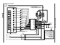
See the attached schematic for clarification.
Sleep
The converter can be put into ‘sleep’ mode by connecting pin
15 to either of the converter’s supply voltages. For normal
operation, it is recommended that pin 15 be tied to ground.
However, the sleep pin does have an active pulldown
current, so the pin can be left disconnected for normal
operation. On the evaluation board, jumper J1 is provided for
controlling the sleep pin. Remove the jumper from J1 for
normal operation and replace it for sleep mode.
Power Supply(s) and Ground(s)
The user can operate from either a single supply or dual
supplies. The DAC is designed to function with the digital
and analog voltages at the same value. The evaluation
board contains two power supply connections to allow for
measuring the current drawn from the digital and analog
sections independently. For single supply mode, it is
recommended that a single power supply wire be attached
to either DVDD1 or AVDD1, and then a jumper wire placed
from E2 to E3 (holes). A single ground wire should be
attached to either DCOM1 or ACOM1 from the power supply.
These grounds are identical, as the evaluation board uses a
single ground plane. The user can select to use dual ground
planes in their design connected at a single point near the
converter (this is the recommended configuration). For dual
supply mode, connect a power supply wire to both AVDD1
and DVDD1 and ground wires to DCOM1 and ACOM1
independently.
Getting Started
A summary of the external supplies, equipment, and signal
sources needed to operate the board is given below:
1. +5V for HI5760.
2. Data generator capable of generating 10-bit patterns. The
HSP-EVAL with the HSP45116 NCOM daughter board is
an option (see ‘Learning Your Way Around’).
3. Square wave clock source (usually part of the Data
Generator).
4. Spectrum analyzer or oscilloscope for viewing the output
of the converter.
Attach a +5V power supply to the evaluation board. Connect
the 10 input bits from the data generator to the evaluation
board, preferably by using a male, 64 or 96-pin VME (Versa
Module Eurocard) connector that mates with the eval board.
Connect the clock source to the eval board, also preferably
through the 64-pin connector. Failure to make clean and
short connections to the data input lines and clock source
will result in a decrease in spectral performance.