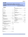
1
User’s
Manual
Sequence CPU Instruction Manual
- Functions (for F3SP22-0S, F3SP28-3N/3S,
F3SP38-6N/6S, F3SP53-4H/4S, F3SP58-6H/6S, F3SP59-7S)
IM 34M06P13-01E
IM 34M06P13-01E
Yokogawa Electric Corporation
4th Edition
Blank Page
i
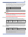
Applicable Product
Range-free Multi-controller FA-M3
-
Model Name: F3SP22, F3SP28, F3SP38, F3SP53, F3SP58, F3SP59
-
Name: Sequence CPU Modules
The document number and document model code for this manual are given below.
Refer to the document number in all communications, including when purchasing
additional copies of this manual.
Document No.
Document Model Code
:
:
Media No. IM 34M06P13-01E (CD)
4th Edition : Jan. 31, 2012 (YHQ)
All Rights Reserved Copyright © 1992, Yokogawa Electric Corporation
IM 34M06P13-01E
DOCIM
IM 34M06P13-01E
4th Edition : Jan. 31, 2012-00
ii
Important
About This Manual
-
This Manual should be passed on to the end user.
Before using the controller, read this manual thoroughly to have a clear
understanding of the controller.
This manual explains the functions of this product, but there is no guarantee that
they will suit the particular purpose of the user.
Under absolutely no circumstances may the contents of this manual be transcribed
or copied, in part or in whole, without permission.
The contents of this manual are subject to change without prior notice.
Every effort has been made to ensure accuracy in the preparation of this manual.
However, should any errors or omissions come to the attention of the user, please
contact the nearest Yokogawa Electric representative or sales office.
Safety Precautions when Using/Maintaining the Product
-
The following safety symbols are used on the product as well as in this manual.
Danger. This symbol on the product indicates that the operator must follow the
instructions laid out in this user’s manual to avoid the risk of personnel injuries,
fatalities, or damage to the instrument. Where indicated by this symbol, the manual
describes what special care the operator must exercise to prevent electrical shock
or other dangers that may result in injury or the loss of life.
Protective Ground Terminal. Before using the instrument, be sure to ground this
terminal.
Function Ground Terminal. Before using the instrument, be sure to ground this
terminal.
Alternating current. Indicates alternating current.
Direct current. Indicates direct current.
IM 34M06P13-01E
4th Edition : Jan. 31, 2012-00
iii
The following symbols are used only in the user’s manual.
WARNING
Indicates a “Warning”.
Draws attention to information essential to prevent hardware damage, software
damage or system failure.
CAUTION
Indicates a “Caution”
Draws attention to information essential to the understanding of operation and
functions.
TIP
Indicates a “TIP”
Gives information that complements the present topic.
SEE ALSO
Indicates a “SEE ALSO” reference.
Identifies a source to which to refer.
-
-
For the protection and safe use of the product and the system controlled by it, be
sure to follow the instructions and precautions on safety stated in this manual
whenever handling the product. Take special note that if you handle the product in
a manner other than prescribed in these instructions, the protection feature of the
product may be damaged or impaired. In such cases, Yokogawa cannot guarantee
the quality, performance, function and safety of the product.
When installing protection and/or safety circuits such as lightning protection devices
and equipment for the product and control system as well as designing or installing
separate protection and/or safety circuits for fool-proof design and fail-safe design of
processes and lines using the product and the system controlled by it, the user
should implement it using devices and equipment, additional to this product.
-
If component parts or consumable are to be replaced, be sure to use parts specified
by the company.
-
This product is not designed or manufactured to be used in critical applications
which directly affect or threaten human lives and safety — such as nuclear power
equipment, devices using radioactivity, railway facilities, aviation equipment,
shipboard equipment, aviation facilities or medical equipment. If so used, it is the
user’s responsibility to include in the system additional equipment and devices that
ensure personnel safety.
-
Do not attempt to modify the product.
Exemption from Responsibility
-
Yokogawa Electric Corporation (hereinafter simply referred to as Yokogawa Electric)
makes no warranties regarding the product except those stated in the WARRANTY
that is provided separately.
-
Yokogawa Electric assumes no liability to any party for any loss or damage, direct or
indirect, caused by the use or any unpredictable defect of the product.
IM 34M06P13-01E
4th Edition : Jan. 31, 2012-00
iv
Software Supplied by the Company
-
Yokogawa Electric makes no other warranties expressed or implied except as
provided in its warranty clause for software supplied by the company.
-
Use the software with one computer only. You must purchase another copy of the
software for use with each additional computer.
Copying the software for any purposes other than backup is strictly prohibited.
-
Store the original media that contain the software in a safe place.
Reverse engineering, such as decompiling of the software, is strictly prohibited.
-
Under absolutely no circumstances may the software supplied by Yokogawa Electric
be transferred, exchanged, or sublet or leased, in part or as a whole, for use by any
third party without prior permission by Yokogawa Electric.
IM 34M06P13-01E
4th Edition : Jan. 31, 2012-00
v
General Requirements for Using the FA-M3 Controller
Avoid installing the FA-M3 controller in the following locations:
-
-
Where the instrument will be exposed to direct sunlight, or where the operating
temperature exceeds the range 0°C to 55°C (32°F to 131°F).
Where the relative humidity is outside the range 10 to 90%, or where sudden
temperature changes may occur and cause condensation.
Where corrosive or flammable gases are present.
-
Where the instrument will be exposed to direct mechanical vibration or shock.
Where the instrument may be exposed to extreme levels of radioactivity.
-
Use the correct types of wire for external wiring:
-
Use copper wire with temperature ratings greater than 75°C.
Securely tighten screws:
-
Securely tighten module mounting screws and terminal screws to avoid problems
such as faulty operation.
-
Tighten terminal block screws with the correct tightening torque as given in this
manual.
Securely lock connecting cables:
-
Securely lock the connectors of cables, and check them thoroughly before turning
on the power.
Interlock with emergency-stop circuitry using external relays:
-
Equipment incorporating the FA-M3 controller must be furnished with emergencystop circuitry that uses external relays. This circuitry should be set up to interlock
correctly with controller status (stop/run).
Ground for low impedance:
-
For safety reasons, connect the [FG] grounding terminal to a Japanese Industrial
Standards (JIS) Class D Ground*1 (Japanese Industrial Standards (JIS) Class 3
Ground). For compliance to CE Marking, use braided or other wires that can ensure
low impedance even at high frequencies for grounding.
*1 Japanese Industrial Standard (JIS) Class D Ground means grounding resistance of 100 Ω max.
Configure and route cables with noise control considerations:
-
Perform installation and wiring that segregates system parts that may likely become
noise sources and system parts that are susceptible to noise. Segregation can be
achieved by measures such as segregating by distance, installing a filter or
segregating the grounding system.
Configure for CE Marking Conformance:
-
For compliance to CE Marking, perform installation and cable routing according to
the description on compliance to CE Marking in the “Hardware Manual”
(IM 34M06C11-01E).
IM 34M06P13-01E
4th Edition : Jan. 31, 2012-00
vi
Keep spare parts on hand:
-
Stock up on maintenance parts including spare modules, in advance.
-
Preventive maintenance (replacement of the module or its battery) is required for
using the module beyond 10 years. For enquiries on battery replacement service
(for purchase), contact your nearest Yokogawa Electric representative or sales
office. (The module has a built-in lithium battery. Lithium batteries may exhibit
decreased voltage, and in rare cases, leakage problems after 10 years.)
Discharge static electricity before operating the system:
-
Because static charge can accumulate in dry conditions, first touch grounded metal
to discharge any static electricity before touching the system.
Never use solvents such as paint thinner for cleaning:
-
Gently clean the surfaces of the FA-M3 controller with a cloth that has been soaked
in water or a neutral detergent and wringed.
-
Do not use volatile solvents such as benzine or paint thinner or chemicals for
cleaning, as they may cause deformity, discoloration, or malfunctioning.
Avoid storing the FA-M3 controller in places with high temperature or
humidity:
-
Since the CPU module has a built-in battery, avoid storage in places with high
temperature or humidity.
-
Since the service life of the battery is drastically reduced by exposure to high
temperatures, take special care (storage temperature should be from –20°C to
75°C).
-
There is a built-in lithium battery in a CPU module and temperature control module
which serves as backup power supply for programs, device information and
configuration information. The service life of this battery is more than 10 years in
standby mode at room temperature. Take note that the service life of the battery
may be shortened when installed or stored at locations of extreme low or high
temperatures. Therefore, we recommend that modules with built-in batteries be
stored at room temperature.
Always turn off the power before installing or removing modules:
-
Failing to turn off the power supply when installing or removing modules, may result
in damage.
Do not touch components in the module:
-
In some modules you can remove the right-side cover and install ROM packs or
change switch settings. While doing this, do not touch any components on the
printed-circuit board, otherwise components may be damaged and modules may fail
to work.
Do not use unused terminals:
-
Do not connect wires to unused terminals on a terminal block or in a connector.
Doing so may adversely affect the functions of the module.
IM 34M06P13-01E
4th Edition : Jan. 31, 2012-00
vii
Waste Electrical and Electronic Equipment
Waste Electrical and Electronic Equipment (WEEE), Directive 2002/96/EC
(This directive is only valid in the EU.)
This product complies with the WEEE Directive (2002/96/EC) marking requirement.
The following marking indicates that you must not discard this electrical/electronic
product in domestic household waste.
Product Category
With reference to the equipment types in the WEEE directive Annex 1, this product is
classified as a “Monitoring and Control instrumentation” product.
Do not dispose in domestic household waste.
When disposing products in the EU, contact your local Yokogawa Europe B. V. office.
How to Discard Batteries
The following description on DIRECTIVE 2006/66/EC (hereinafter referred to as the EU
new directive on batteries) is valid only in the European Union.
Some models of this product contain batteries that cannot be removed by the user.
Make sure to dispose of the batteries along with the product.
Do not dispose in domestic household waste.
When disposing products in the EU, contact your local Yokogawa Europe B. V. office.
Battery type: Lithium battery
Note: The symbol above means that the battery must be collected separately as
specified in Annex II of the EU new directive on batteries.
IM 34M06P13-01E
4th Edition : Jan. 31, 2012-00
viii
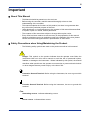
Introduction
Overview of the Manual
This manual describes the sequencing functions of sequence CPU modules
(For F3SP22, F3SP28-3N/3S, F3SP38-6N/6S, F3SP53-4H/4S, F3SP58-6H/6S,
F3SP59-7S) designed for use with the Range-free Multi-controller FA-M3.
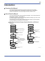
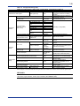
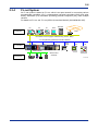
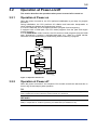
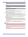
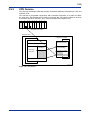
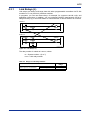
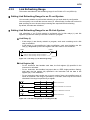
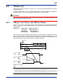
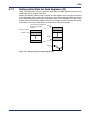
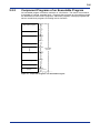
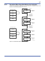
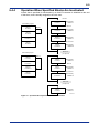
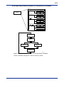
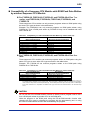
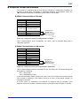
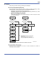
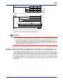
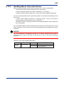
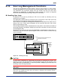
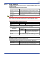
How to Read the Manual
If you are a first-time reader, first go through this paragraph, “How to Read the Manual,”
and proceed to Chapter 1, then Chapter 3.
For efficiency, read only the relevant remaining chapters according to your flow of work
from system design to system operation.
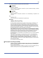
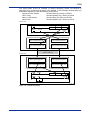
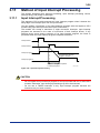
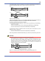
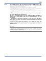
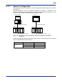
The chart below shows the regular workflow, from system design to system operation,
as well as chapters you should refer to in each step.
Work Flow from System Design to System Operation, and Relevant
Chapters
Target machine
Design
Start
Start
Determination of system configuration
System design
Chapter 2, "System Configuration"
Wiring
Assignment of I/Os, registers and relays
Basic design
Chapter 4, "Devices," and
Chapter 5, "Programs"
I/O verification
Input: Verification of I/Os with
LED lamps
Output: Forced SET and
RESET instructions
Chapter 6, "Functions"
Program downloading
Coding
Programming
Configuration of a ladder diagram
Ladder symbols
Mnemonic language
Chapter 1, "General Description,"
Chapter 2, "Basic Instructions," and
Chapter 3, "Application Instructions,"
of “Sequence CPU Instruction Manual –
Instructions” 3rd or later edition.
Program input for
simulation
Performance check
?
End
Verification of basic logic
Program modification
Debugging
Trial operation
?
End
Program modification
Chapter 6, "Functions"
End of flow?
Program storage on floppy/
hard disk or in ROM pack
Chapter 6, "Functions"
End of flow?
Program storage on floppy/hard
disk or in ROM pack
F000001.VSD
IM 34M06P13-01E
4th Edition : Jan. 31, 2012-00
ix
Other User’s Manuals
Be sure to read each of the following manuals, in addition to this manual.
For information on the instructions used with sequence CPUs, refer to:
-
Sequence CPU Instruction Manual – Instructions (IM 34M06P12-03E)
For information on the commands and responses of personal computer
link functions
-
Personal Computer Link Commands (IM 34M06P41-01E).
When creating programs using ladder language, refer to:
-
FA-M3 Programming Tool WideField3 (IM 34M06Q16-
E)
or
- FA-M3 Programming Tool WideField2 (IM 34M06Q15-01E)
-
FA-M3 Programming Tool WideField (IM 34M06Q14-01E); and
FA-M3 Programming Tool WideField - Application (IM 34M06Q14-02E).
For information on the specifications*, configuration*, installation,
wiring, trial operation, maintenance and inspection of the FA-M3, as
well as information on the system-wide limitation of module installation,
refer to:
*:
Hardware Manual (IM 34M06C11-01E).
For information on the specifications of products other than the power supply module, base module, I/O module, cable
and terminal block unit, refer to their respective user’s manuals.
Read the following user’s manuals, as required.
For information on the functions of F3SP21, F3SP25 and F3SP35
sequence CPU modules, refer to:
-
Sequence CPU - Functions (for F3SP21, F3SP25 and F3SP35)
(IM 34M06P12-02E).
For information on the functions of fiber-optic FA-bus modules, refer to:
-
Fiber-optic FA-bus Module and Fiber-optic FA-bus Type 2 Module, FA-bus Type 2
Module (IM 34M06H45-01E).
For information on the functions of FA link H and fiber-optic FA link H
modules, refer to:
-
FA Link H Module, Fiber-optic FA Link H Module (IM 34M06H43-01E).
For information on the FL-net functions, refer to:
-
FL-net (OPCN-2) Interface Module (IM 34M06H32-02E).
For information on the functions of BASIC CPU modules, refer to:
-
BASIC CPU Modules and YM-BASIC/FA Programming Language
(IM 34M06Q22-01E).
IM 34M06P13-01E
4th Edition : Jan. 31, 2012-00
x
Copyrights and Trademarks
Copyrights
Copyrights of the programs and online manual included in this CD-ROM belong to
Yokogawa Electric Corporation.
This online manual may be printed but PDF security settings have been made to prevent
alteration of its contents.
This online manual may only be printed and used for the sole purpose of operating this
product. When using a printed copy of the online manual, pay attention to possible
inconsistencies with the latest version of the online manual. Ensure that the edition
agrees with the latest CD-ROM version.
Copying, passing, selling or distribution (including transferring over computer networks)
of the contents of the online manual, in part or in whole, to any third party, is strictly
prohibited. Registering or recording onto videotapes and other media is also prohibited
without expressed permission of Yokogawa Electric Corporation.
Trademarks
The trade and company names that are referred to in this document are either
trademarks or registered trademarks of their respective companies.
IM 34M06P13-01E
4th Edition : Jan. 31, 2012-00
TOC-1
FA-M3
Sequence CPU Instruction Manual - Functions
(for F3SP22-0S, F3SP28-3N/3S, F3SP38-6N/6S, F3SP53-4H/4S, F3SP58-6H/6S,
IM 34M06P13-01E 4th Edition
F3SP59-7S)
CONTENTS
Applicable Product ....................................................................................i
Important ...................................................................................................ii
Introduction............................................................................................viii
Copyrights and Trademarks ....................................................................x
1.
Specifications and Basic Configuration ................................... 1-1
1.1
1.2
1.3
2.
System Configuration ................................................................ 2-1
2.1
2.2
2.3
2.4
3.
Overview .............................................................................................. 1-1
Specifications...................................................................................... 1-3
1.2.1
List of Specifications ............................................................... 1-3
1.2.2
Device List .............................................................................. 1-6
1.2.3
Configuration .......................................................................... 1-7
1.2.4
Components and Their Functions..........................................1-11
1.2.5
External Dimensions............................................................. 1-12
Basic Configuration.......................................................................... 1-13
1.3.1
Unit........................................................................................ 1-13
1.3.2
Slot Number.......................................................................... 1-14
1.3.3
I/O Relay Number ................................................................. 1-15
Basic System Configuration .............................................................. 2-1
Multi-CPU System Configuration ...................................................... 2-1
2.2.1
Multi-CPU System Configuration............................................ 2-1
2.2.2
Handling I/O Modules in Multi-CPU System........................... 2-3
Extended System Configuration ....................................................... 2-4
2.3.1
Remote I/O System ................................................................ 2-4
2.3.2
Personal Computer Link System ............................................ 2-5
2.3.3
FA Link System ....................................................................... 2-5
2.3.4
FL-net System ........................................................................ 2-6
Programming Tool .............................................................................. 2-7
2.4.1
WideField3/WideField2........................................................... 2-7
Basic Operations of Sequence CPU Module............................ 3-1
3.1
3.2
3.3
Operating Modes of Sequence CPU Module.................................... 3-1
Operation at Power-on/off.................................................................. 3-2
3.2.1
Operation at Power-on............................................................ 3-2
3.2.2
Operation at Power-off............................................................ 3-2
Operation in Case of Momentary or Complete Power Failure........ 3-3
IM 34M06P13-01E
4th Edition : Jan. 31, 2012-00
TOC-2
3.4
3.5
3.6
3.7
3.8
3.9
3.10
3.11
4.
3.3.1
Operation in Case of Momentary Power Failure .................... 3-3
3.3.2
Momentary Power Failure Detection Mode Setup.................. 3-4
3.3.3
Operation in Case of Complete Power Failure ....................... 3-4
3.3.4
Data Latch Range at Power Failure ....................................... 3-4
Operation Processing Method........................................................... 3-5
Method of Executing Peripheral Processes..................................... 3-7
Method of I/O Processing................................................................... 3-8
3.6.1
Method of I/O Processing ....................................................... 3-8
3.6.2
Response Delay ..................................................................... 3-9
3.6.3
I/O Processing in Multi-CPU System.................................... 3-10
Method of Executing Commands from WideField3....................... 3-11
3.7.1
Tool Service ...........................................................................3-11
Method of Executing Commands through
Personal Computer Link .................................................................. 3-12
3.8.1
Personal Computer Link Service .......................................... 3-12
Method of CPU-to-CPU Data Communication................................ 3-13
3.9.1
Method of Updating Shared Data ......................................... 3-13
3.9.2
Configuration of Shared Refreshing ..................................... 3-15
3.9.3
CPU Service ......................................................................... 3-19
Method of Link Data Updating ......................................................... 3-20
3.10.1 Link Data Updating ............................................................... 3-20
3.10.2 Link Refreshing..................................................................... 3-21
Method of Input Interrupt Processing............................................. 3-26
3.11.1 Input Interrupt Processing..................................................... 3-26
3.11.2 Input Interrupt Processing Control........................................ 3-27
3.11.3 Interrupt Timing..................................................................... 3-28
3.11.4 Priority of Interrupts .............................................................. 3-30
Devices ........................................................................................ 4-1
4.1
4.2
4.3
4.4
I/O Relays (X/Y) ................................................................................... 4-1
4.1.1
Input Relays (X) ...................................................................... 4-1
4.1.2
Output Relays (Y) ................................................................... 4-2
4.1.3
Allocation of I/O Addresses .................................................... 4-2
4.1.4
Configuring DIO Modules ....................................................... 4-3
Internal Relays (I), Shared Relays (E) and Extended Shared
Relays (E)............................................................................................. 4-6
4.2.1
Internal Relays (I) ................................................................... 4-6
4.2.2
Shared Relays (E) and Extended Shared Relays (E) ............ 4-7
Link Relays (L) and Link Registers (W) .......................................... 4-11
4.3.1
Link Relays (L)...................................................................... 4-12
4.3.2
Link Registers (W) ................................................................ 4-13
4.3.3
System Numbers .................................................................. 4-14
4.3.4
Configuring Link Relays (L) and Registers (W) .................... 4-15
4.3.5
Link Refreshing Range ......................................................... 4-16
Special Relays (M) ............................................................................ 4-18
4.4.1
Block Start Status Relays...................................................... 4-18
4.4.2
Utility Relays ......................................................................... 4-19
4.4.3
Sequence Operation and Mode Status Relays..................... 4-20
IM 34M06P13-01E
4th Edition : Jan. 31, 2012-00
TOC-3
4.5
4.6
4.7
4.8
4.9
4.10
5.
Programs..................................................................................... 5-1
5.1
5.2
5.3
6.
4.4.4
Self-diagnosis Status Relays ................................................ 4-21
4.4.5
FA Link Module Status Relays .............................................. 4-22
4.4.6
FL-net Interface Module Status Relays ................................ 4-22
Timers (T)........................................................................................... 4-23
4.5.1
100-µs, 1-ms, 10-ms, and 100-ms Timers............................ 4-23
4.5.2
100-ms Continuous Timer..................................................... 4-24
4.5.3
Selecting Timers ................................................................... 4-25
Counters (C) ...................................................................................... 4-26
4.6.1
Selecting Counters ............................................................... 4-27
Data Register (D), Shared Register (R) and Extended Shared
Register (R)........................................................................................ 4-28
4.7.1
Data Registers (D) ................................................................ 4-28
4.7.2
Shared Registers (R) and Extended Shared Registers (R).. 4-29
4.7.3
Setting Initial Data for Data Registers (D) ............................ 4-33
Special Registers (Z) ........................................................................ 4-35
4.8.1
Sequence Operation Status Registers ................................. 4-35
4.8.2
Self-diagnosis Status Registers............................................ 4-35
4.8.3
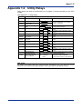
Utility Registers..................................................................... 4-36
4.8.4
FA Link Module Status Registers.......................................... 4-38
4.8.5
Sequence CPU Module Status Registers............................. 4-39
Index Registers (V) ........................................................................... 4-40
File Registers (B) .............................................................................. 4-41
Programming Language..................................................................... 5-1
5.1.1
Structured Ladder Language .................................................. 5-1
5.1.2
Mnemonic Language .............................................................. 5-1
Program Types and Configuration.................................................... 5-2
5.2.1
Blocks and Executable Programs........................................... 5-2
5.2.2
Component Programs of an Executable Program.................. 5-4
Program Memory ................................................................................ 5-9
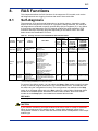
Functions .................................................................................... 6-1
6.1
6.2
6.3
6.4
6.5
6.6
Function List ....................................................................................... 6-1
Operation Setup Functions................................................................ 6-2
Constant Scan ..................................................................................... 6-4
6.3.1
Setting the Constant Scan Time ............................................. 6-4
Executing All Blocks/Specified Blocks............................................. 6-5
6.4.1
Executing All Blocks................................................................ 6-5
6.4.2
Executing Specified Blocks..................................................... 6-6
6.4.3
Operation When Specified Blocks Are Activated .................... 6-7
6.4.4
Operation When Specified Blocks Are Inactivated ................. 6-9
6.4.5
Operation When Specified Blocks Are Executed.................. 6-10
Debugging Functions ....................................................................... 6-12
6.5.1
Forced SET/RESET.............................................................. 6-12
6.5.2
Changing Setpoints, Current Values and Data Values ....... 6-12
6.5.3
Stopping Refreshing ............................................................. 6-13
Program Protection .......................................................................... 6-14
IM 34M06P13-01E
4th Edition : Jan. 31, 2012-00
TOC-4
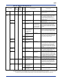
6.7
6.8
6.9
6.10
6.11
6.12
6.13
6.14
6.15
6.16
6.17
6.18
6.19
7.
6.6.1
Executable Program Protection............................................ 6-14
6.6.2
Block Protection.................................................................... 6-15
Online Editing.................................................................................... 6-16
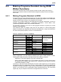
Making Programs Resident Using ROM Writer Functions ........... 6-18
6.8.1
Making Programs Resident in ROM ..................................... 6-18
6.8.2
Defining Current Values of Devices to Be Made Resident
in ROM.................................................................................. 6-21
6.8.3
ROM Writer Functions and ROM Writer Mode ................... 6-21
Exclusive Access Control ................................................................ 6-23
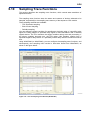
Sampling Trace Functions ............................................................... 6-24
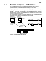
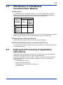
Personal Computer Link Functions ................................................ 6-27
6.11.1 System Configuration ........................................................... 6-28
6.11.2 Differences from Personal Computer Link Module............... 6-29
6.11.3 Specifications of Personal Computer Link Functions ........... 6-30
6.11.4 Setting Up the Personal Computer Link Functions .............. 6-31
6.11.5 Communication Procedure ................................................... 6-32
6.11.6 Commands and Responses ................................................. 6-34
Device Management Functions ....................................................... 6-42
Macro Instructions............................................................................ 6-43
6.13.1 What Are Macro Instructions? .............................................. 6-43
6.13.2 Specification of Macro Instructions ....................................... 6-46
6.13.3 Devices Dedicated to Macro Instructions ............................. 6-47
6.13.4 Nesting Macro Instructions ................................................... 6-50
6.13.5 Handling Macro Instruction Errors ........................................ 6-52
6.13.6 Protecting Macro Instructions ............................................... 6-53
6.13.7 Debugging Operation............................................................ 6-53
6.13.8 Input Macro Instructions ....................................................... 6-54
6.13.9 Structure Macro Instructions................................................. 6-56
User Log Management Functions ................................................... 6-58
Sensor Control Functions................................................................ 6-59
6.15.1 Schematic Operation Diagram ............................................. 6-59
6.15.2 Features................................................................................ 6-60
6.15.3 Specifications and Restrictions............................................. 6-60
6.15.4 Functions .............................................................................. 6-64
6.15.5 Procedures for Using Sensor Control Functions .................. 6-69
6.15.6 Error Handling....................................................................... 6-70
6.15.7 Programming Precautions .................................................... 6-71
Partial Download Functions............................................................. 6-73
Functions for Storing Comments to CPU....................................... 6-74
6.17.1 Performing Setup to Download Comments .......................... 6-74
6.17.2 Number of Steps Needed for Comments.............................. 6-75
6.17.3 Online Editing of Comments ................................................. 6-76
Functions for Storing Tag Name Definitions to CPU..................... 6-77
Structures .......................................................................................... 6-78
I/O Response Time Based on Scan Time ................................. 7-1
7.1
Description of Scan Time................................................................... 7-1
IM 34M06P13-01E
4th Edition : Jan. 31, 2012-00
TOC-5
7.2
7.3
7.4
7.5
8.
RAS Functions............................................................................ 8-1
8.1
8.2
9.
Self-diagnosis ..................................................................................... 8-1
8.1.1
Setting Error-time Action (Operating Mode in Case of
Error)....................................................................................... 8-5
Updating Error Status Indicators after Correcting Moderate or
Minor Failures ..................................................................................... 8-6
Differences from F3SP25 and F3SP35 Sequence CPUs ......... 9-1
9.1
9.2
9.3
9.4
9.5
9.6
10.
Setting Scan Monitoring Time ........................................................... 7-4
Examples of Scan Time Calculation ................................................. 7-4
Example of I/O Response Time Calculation..................................... 7-6
Instruction Execution Time................................................................ 7-7
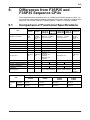
Comparison of Functional Specifications ........................................ 9-1
Configuration ...................................................................................... 9-3
Special Relays (M) and Special Registers (Z) .................................. 9-4
CPU Module to CPU Module Communication Method.................... 9-5
High-speed Processing of Application Instructions ....................... 9-5
Instructions ......................................................................................... 9-6
Difference between F3SP
10.1
10.2
10.3
10.4
Appendix 1.
- N/- H ..... 10-1
Partial Download Functions............................................................. 10-1
Storing Comments or Tag Name Definitions in CPU..................... 10-1
New Instructions and Instruction Related Functions ................... 10-2
Changes in Specifications ............................................................... 10-3
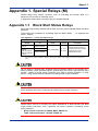
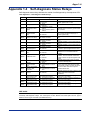
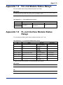
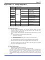
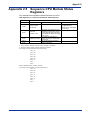
Special Relays (M)...............................................Appx.1-1
Appendix 1.1
Appendix 1.2
Appendix 1.3
Appendix 1.4
Appendix 1.5
Appendix 1.6
Appendix 2.
- S and F3SP
Block Start Status Relays............................................ Appx.1-1
Utility Relays................................................................. Appx.1-2
Sequence Operation and Mode Status Relays.......... Appx.1-3
Self-diagnosis Status Relays ...................................... Appx.1-4
FA Link Module Status Relays .................................... Appx.1-5
FL-net Interface Module Status Relays...................... Appx.1-5
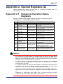
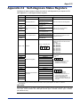
Special Registers (Z)...........................................Appx.2-1
Appendix 2.1
Appendix 2.2
Appendix 2.3
Appendix 2.4
Appendix 2.5
Sequence Operation Status Registers....................... Appx.2-1
Self-diagnosis Status Registers ................................. Appx.2-2
Utility Registers............................................................ Appx.2-3
FA Link Module Status Registers ............................... Appx.2-4
Sequence CPU Module Status Registers .................. Appx.2-5
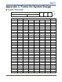
Appendix 3. Forms for System Design...................................Appx.3-1
Program Coding Sheet .............................................................Appx.3-1
Relay Devices Assignment Table ............................................Appx.3-2
Register Devices Assignment Table........................................Appx.3-3
Timer/Counter Setpoints Table ................................................Appx.3-4
Index .............................................................................................. Index-1
IM 34M06P13-01E
4th Edition : Jan. 31, 2012-00
TOC-6
Revision Information .................................................................................i
IM 34M06P13-01E
4th Edition : Jan. 31, 2012-00
1-1
1.
Specifications and Basic
Configuration
This chapter explains the CPU module specifications and the basic configuration
of the Range-free Multi-controller FA-M3.
1.1
Overview
This section describes the overview, features and main functions of the sequence CPU
module.
Overview
Models F3SP28-3N, F3SP38-6N, F3SP53-4H, F3SP58-6H, F3SP22-0S, F3SP28-3S,
F3SP38-6S, F3SP53-4S, F3SP58-6S and F3SP59-7S are CPU modules with built-in
memory for use with the Range-free Multi-controller FA-M3.
In addition to high-speed operation and large memory capacity, these modules have
many more features that help increase development and maintenance efficiency.
Features
z High-speed Operation
-
20K steps/1 ms, with shortest scan interval of 200 μs
High-speed I-P-R-S, which means:
- High-speed Instruction
- High-speed Performance
- High-speed Response
- High-speed Scan
z Sensor Control Functions
In addition to normal scanning, each CPU module has an independent, multiple constant
scan function, permitting fast scanning. Fast response is also achievable with a single
CPU.
You can execute a block of your program at a high-speed constant scan (200 μsminimum), separately from normal scanning. This feature enables you to eliminate the
effects of a fault diagnosis program or MMI program, as well as ensure stable control
program operation.
z Object Ladder
The FA-M3 Programming Tool WideField3, an object-oriented ladder language
development tool, is available with the CPU module. This tool not only increases
software development productivity over and above structured programming, but also
simplifies program maintenance.
z Function for Storing Comments [F3SP-S]
Circuit comments, subcomments, and tag name definitions (including I/O comments)
can be stored in the sequence CPU or the ROM pack. This function allows you to debug
a program using tag names, even during unscheduled maintenance.
IM 34M06P13-01E
4th Edition : Jan. 31, 2012-00
1-2
z Other Features
-
-
A compact body allows for reduced panel enclosure size.
Large-capacity programs and large device sizes are supported to cope with
advanced, complex control applications.
Index modification and structured ladder language simplifies program design and
maintenance.
The device size and operating method can be flexibly configured to suit your
application needs.
A rich set of functions are provided to facilitate program debugging and
maintenance. For example, a forced SET/RESET function independent of program
operation results.
A carefully designed self-diagnosis function supplements a highly reliable design.
Macro instruction functions allow you to create and register new instructions.
The sampling trace functions acquire and displays the states of multiple devices for
a maximum of 1024 scans.
The programming tool connection port supports the personal computer link
functions and thus enables connection to a higher-level computer or a monitor
without the need for a personal computer link module.
The log function records errors encountered in a program, as well as messages
created and registered in advance.
F3SP22, F3SP28, F3SP38, F3SP53, F3SP58 or F3SP59 modules can be mounted
in slots 2 to 4 of the main unit, for use as add-on CPU modules for sequence
processes added to the main CPU module (F3SP21, F3SP22, F3SP25, F3SP28,
F3SP35, F3SP38, F3SP53, F3SP58 F3SP59, F3SP66, F3SP67, F3SP71, or
F3SP76).
A ROM pack can be attached so that you can perform ROM-based operation and
store programs.
Program protection functions ensure security.
The partial download functions allow downloading of specified blocks only, which
increases debugging efficiency especially in collaborative program development.
[F3SP-S]
Indirect specification via devices enables large volume data handling and creation of
efficient programs. [F3SP-S]
Structure macros simplify passing of data to macros and updating of these data
structures. [F3SP-S]
Functions
-
Sensor control
Configuration (setup of parameters, including device size, range of devices to be latched
in case of power failure, and external output to be retained in case of sequence stop)
- Constant scan (at an interval of 1 to 190 ms, in 0.1 ms increments)
- Sampling trace
- Debugging (forced SET/RESET instructions, online editing, etc.)
- Error logging, user logging
- Clock (year, month, day, hour, minute, second, and day of week)
- Support for programming tool connection port with the personal computer link functions
- Program protection
- Program/data storage in ROM pack
- Circuit/sub-comment, tag name definitions storage in ROM pack [F3SP-S]
- Circuit/sub-comment storage function and tag name definition storage function
[F3SP-S]
- Partial download functions [F3SP-S]
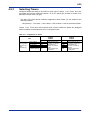
See Section 1.2, “Specifications,” for more information.
IM 34M06P13-01E
4th Edition : Jan. 31, 2012-00
1-3
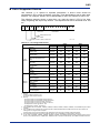
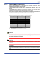
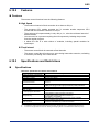
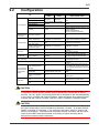
1.2
Specifications
This section describes the basic specifications of the FA-M3 sequence CPU module for
each CPU type. For functional specifications, see Section 1.2.1, "List of Specifications."
For the types and number of devices, see Section 1.2.2, "Device List." For configuration
setup ranges, see Section 1.2.3, "Configuration."
For the names and functions of the components of the sequence CPU module, see
Section 1.2.4, "Components and Their Functions." For the external dimensions of the
sequence CPU module, see Section 1.2.5, "External Dimensions."
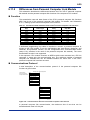
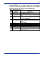
1.2.1
List of Specifications
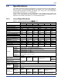
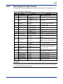
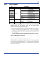
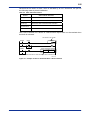
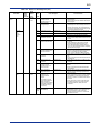
Table 1.1 Functional Specification (F3SP-S) (1/2)
Specifications
Item
Control method
I/O method
Programming language
Number of I/O points
Number of internal relays (I)
Number of shared relays (E)
Number of extended shared
relays (E)
Number of link relays (L)
Number of special relays (M)
Number of timers (T)
Number of counters (C)
Number of data registers (D)
Number of shared registers (R)
Number of extended shared
registers (R)
Number of file registers (B)
Number of link registers (W)
Number of special registers (Z)
Number of labels
Number of input interrupt
processing routines
Decimal
constant
Hexadecimal
constant
CharacterConstants
string constant
IEEE singleprecision
floating-point
constant
Index constant
Program size
(ROM resident)
(Program + Tag Name Definition)
size
ROM-resident size
(Program + Tag Name Definition)
Number of program blocks
Basic
Number of
instructions
instructions
Application
instructions
Number of macro instructions
Instruction
execution time
Basic
instruction
Application
instruction
F3SP22-0S
F3SP28-3S
F3SP53-4S
F3SP38-6S
F3SP58-6S
F3SP59-7S
Repetitive operation based on stored programs
Refresh method/Direct I/O instruction
Structured ladder language and mnemonic language
4096 max.
8192 max. (including remote I/O points)
16384
16384
16384
32768
32768
65535
2048
2048
2048
2048
2048
2048
2048
2048
2048
2048
2048
2048
8192
9984
8192
9984
8192
9984
16384
9984
16384
9984
16384
9984
2048 in total
2048 in total
2048 in total
3072 in total
3072 in total
3072 in total
16384
1024
16384
1024
16384
1024
32768
1024
32768
1024
1024
3072
3072
3072
3072
3072
3072
32768
8192
1024
1024
32768
8192
1024
1024
32768
8192
1024
1024
262144
16384
1024
1024
262144
16384
1024
1024
262144
16384
1024
1024
4
4
4
4
4
4
16-bit instruction:
32-bit instruction:
16-bit instruction:
32-bit instruction:
16-bit instruction:
32-bit instruction:
65535
-32768 to 32767
-2147483648 to 2147483647
$0 to $FFFF (hexadecimal number)
$0 to $FFFFFFFF (hexadecimal number)
e.g. “AB”
e.g. “ABCD”
32-bit instruction: e.g. 1.23, -3.21
Approximately -3.4×1038 to 3.4×1038
0 to 2047
10K steps
max.
30K steps
max.
56K steps
max.
120K steps max.
120K steps max.
254K steps
max.
360K steps
max.
360K steps max.
1024 max.
37
329
256 max.
0.045 to
0.18µs
per
instruction
0.18 µs per
instruction
0.045 to
0.18µs
per
instruction
0.18 µs per
instruction
0.0175 to
0.07µs
per
instruction
0.07 µs per
instruction
0.045 to
0.18µs
per
instruction
0.18 µs per
instruction
0.0175 to 0.07µs per
instruction
0.07µs per instruction
IM 34M06P13-01E
4th Edition : Jan. 31, 2012-00
1-4
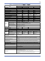
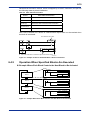
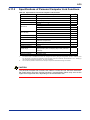
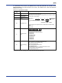
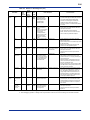
Table 1.2 Functional Specification (F3SP-S) (2/2) (Continued)
Item
Special module High-speed
Read (HRD) Instruction
/special module High-speed
Write (HWR) Instruction
Sampling trace functions
Support for personal computer
link functions by programming
tool connection port
User log functions
Number of personal computer
link modules
Macro instruction functions
Scan monitoring time
Startup at power-on or recovery
from power failure
Sensor control functions
Constant scan time
Self-diagnosis
Link functions
Comment storage functions
Other functions
Specifications
F3SP22-0S
F3SP28-3S
F3SP53-4S
F3SP38-6S
F3SP58-6S
F3SP59-7S
64 instructions each
Available. These functions collect and display the states of multiple devices for a
maximum of 1024 scans.
Available. These functions allow a personal computer or a monitor to be connected to the
programming tool connection port to perform communications equivalent to the personal
computer link module.
Available. These functions allow the user to execute a user log command to log (record
the history of) errors in the user system, including information on the state of occurrence
and system operation, etc.
6 max.
Available. These functions allow the user to create and register new user-defined
instructions.
Variable from 10 to 200 ms.
Automatic (Auto-logging of power-on time, power-off time and momentary power failure
time)
Available. In addition to normal scanning, these functions allow one specified block to be
scanned at high-speed fixed intervals.
1 to 190 ms, configurable in 0.1 ms increments.
Detection of memory failure, CPU failure and I/O module failure, syntax checking, etc.
FA link, FL-net, personal computer link, and remote I/O link (fiber-optic FA-bus, µ-bus)
Available. Circuit comment, sub-comment, tag name definition (including I/O comment).
- Online editing
- Forced SET/RESET instructions
- Clock (year, month, day, hour, minute, second, and day of the week)
- Configuration (setup of parameters, including device capacities, range of devices to be
latched at power failure, and external outputs to be latched at sequence stop)
- Protection
- Stop refreshing function
IM 34M06P13-01E
4th Edition : Jan. 31, 2012-00
1-5
Table 1.3 Functional Specification (F3SP-N, F3SP-H)
Item
Control method
I/O method
Programming language
Number of I/O points
Number of internal relays (I)
Number of shared relays (E)
Number of extended shared relays (E)
Number of link relays (L)
Number of special relays (M)
Number of timers (T)
Number of counters (C)
Number of data registers (D)
Number of shared registers (R)
Number of extended shared registers (R)
Number of file registers (B)
Number of link registers (W)
Number of special registers (Z)
Number of labels
Number of input interrupt processing routines
Decimal constant
Constants
Hexadecimal constant
Character-string constant
Floating-point constant
Program size
(that can be ROM resident)
Number of program blocks
Number of
Basic instructions
instructions
Application instructions
Number of macro instructions
Instruction
execution time
Basic instruction
Application instruction
Special module High-speed Read instruction
(HRD)/special module High-speed Write
instruction (HWR)
Sampling trace functions
Support for personal computer link functions by
programming tool connection port
User logging functions
Number of personal computer link modules
Macro instruction functions
Scan monitoring time
Startup at power-on or recovery from power
failure
Sensor control functions
Constant scan time
Self-diagnosis
Link function
Other functions
Specifications
F3SP28-3N
F3SP53-4H
F3SP38-6N
F3SP58-6H
Repeated operation based on stored programs
Refresh method/Direct I/O instruction
Structured ladder language and mnemonic language
4096 max.
8192 max., including remote I/O points
16384
16384
32768
32768
2048
2048
2048
2048
2048
2048
2048
2048
8192
8192
16384
16384
9984
9984
9984
9984
2048 in total
2048 in total
3072 in total
16384
16384
32768
1024
1024
1024
3072
3072
3072
32768
32768
262144
8192
8192
16384
1024
1024
1024
1024
1024
1024
4
4
4
16-bit instruction: -32768 to 32767
32-bit instruction: -2147483648 to 2147483647
16-bit instruction: $0 to $FFFF (hexadecimal number)
32-bit instruction: $0 to $FFFFFFFF (hexadecimal number)
16-bit instruction: e.g. “AB”, etc
32-bit instruction: e.g. “ABCD”, etc.
32-bit instruction: e.g. 1.23, -3.21
approximately -3.4×1038 to +3.4×1038
30K steps max.
56K steps max.
120K steps max.
1024 max.
33
312
64 max.
0.045 to 0.18 µs
per instruction
0.18 µs min. per
instruction
0.0175 to 0.07 µs
per instruction
0.07 µs min. per
instruction
0.045 to 0.18 µs
per instruction
0.18 µs min. per
instruction
3072 in total
32768
1024
3072
262144
16384
1024
1024
4
0.0175 to 0.07 µs
per instruction
0.07 µs min. per
instruction
64 instructions each
Available. This function collects and displays the states of multiple devices for a maximum of 1024
scans.
Available. The function allows a personal computer or a monitor to be connected to the
programming tool connection port to perform communications equivalent to the personal computer
link module.
Available. These functions allow the user to execute a user log instruction to log (record the history
of) errors in the user system, including information on the state of occurrence and system
operation, etc.
6 max.
Available. These functions allow a user to create and register new user-defined instructions.
Variable from 10 to 200 ms
Automatic (Auto-logging of power-on time, power-off time and momentary power failure time)
Available. In addition to normal scanning, these functions allow one specific block to be scanned at
high-speed fixed intervals.
1 to 190 ms, configurable in 0.1 ms increments
Detection of memory failure, CPU failure and I/O module failure, syntax checking, etc.
FA link, FL-net, personal computer link, and remote I/O link (fiber-optic FA-bus, µ-bus)
- Online editing
- Forced SET/RESET instructions
- Clock (year, month, day, hour, minute, second, and day of the week)
- Configuration (setup of parameters, including device capacities, range of devices to be latched
at power failure, and external outputs to be latched when sequence stops)
- Protection
IM 34M06P13-01E
4th Edition : Jan. 31, 2012-00
1-6
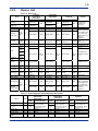
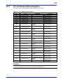
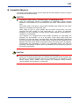
1.2.2
Device List
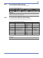
Table 1.4 Device List
Device
Code
Input relay
X
Output relay
Y
Internal relay
Shared relay
I
Extended
shared relay
Link relay
Continuous
timer
Counter
Data register
File register
Link register
Extended
shared register
E2049 to E4096
2048
E2049 to E4096
2048
F3SP59-7S
Quantity
8192
32768
2048
E
Nonlatched
type
L
L0001 to L72048
(discontinuous)
8192
L0001 to L72048
(discontinuous)
16384
M
M0001 to M9984
9984
M0001 to M9984
9984
100 µs
Timer
1 ms
Timer
10 ms
Timer
100 ms
Timer
100 ms
Timer
T
Latched
type
C
C0001 to C2048
D
D00001 to D16384
Latched
type
Latched
type
Nonlatched
type
T0001 to T0016
T0001 to T2048
B
W
Special register
Index register
Shared register
Range
X00201 to X71664
(discontinuous)
Y00201 to Y71664
(discontinuous)
I00001 to I32768
E0001 to E2048
F3SP38-6N/6S
F3SP58-6H/6S
Nonlatched
type
Special relay
Timer
F3SP22-0S
F3SP28-3N/3S
F3SP53-4H/4S
Range
Quantity
X00201 to X71664
(discontinuous)
4096
Y00201 to Y71664
(discontinuous)
I00001 to I16384
16384
E0001 to E2048
2048
Z
V
Nonlatched
type
B000001 to
B32768
W00001 to
W72048
(discontinuous)
Z0001 to Z1024
V001 to V256
T0001 to T0016
2048 in
total
16384
C0001 to C3072
C0001 to C3072
32768
Configuration limit
correlated to Timers
(T) (*1)
D00001 to D65535
65535
1024
256
B000001 to
B262144
W00001 to
W72048
(discontinuous)
Z0001 to Z1024
V001 to V256
R0001 to R1024
1024
R0001 to R1024
1024
R1025 to R4096
3072
R1025 to R4096
3072
1024
256
R0001 to R1024
1024
R1025 to R4096
3072
8192
Configuration limit
3072 in correlated to counters
total (C) (*1).
3072 in T0001 to T3072
total
B000001 to
B262144
W00001 to
W72048
(discontinuous)
Z0001 to Z1024
V001 to V256
32768
Range
Quantity
X00201 to X71664
The range used
(discontinuous)
8192 depends on the
Y00201 to Y71664
module type
(discontinuous)
I00001 to I65535
65535
E0001 to E2048
2048 These devices default
to zero in quantity. Be
sure to configure the
devices when using
E2049 to E4096
2048
the CPU module in a
multi-CPU
configuration.
Used in FA link and
L0001 to L72048
16384 FL-net
(discontinuous)
communications.
M0001 to M9984
9984
Configurable for up to
T0001 to T0016
16 timers
T0001 to T3072
D00001 to D32768
Remarks
262144
16384
262144
16384
Used in FA link and
FL-net
communications.
1024
256
R
These devices default
to zero in quantity. Be
sure to configure the
devices when using
the CPU module in a
multi-CPU
configuration.
*1: See Table 1.5.
Table 1.5 Device Capacities and Configuration Restrictions
Device
F3SP22-0S
F3SP28-3N/3S
F3SP53-4H/4S
Code
Timer
T
Counter
C
Shared relay
Extended Shared relay
Shared register
Extended shared
register
E
E
R
R
Default
Setup Restrictions
value
1024 Total for timers and
counters: 2048 max.
1024 Default value for 100-µs
and 1-ms timers: 0
0
2048 max.
0
2048 max.
0
1024 max.
0
3072 max.
F3SP38-6N/6S
F3SP58-6H/6S
Default
value
2048
F3SP59-7S
Setup Restrictions
0
0
0
Total for timers and
counters: 3072 max.
Default value for 100-µs
and 1-ms timers: 0
2048 max.
2048 max.
1024 max.
0
3072 max.
1024
Default
value
2048
Setup Restrictions
0
0
0
Total for timers and
counters: 3072 max.
Default value for 100-µs
and 1-ms timers: 0
2048 max.
2048 max.
1024 max.
0
3072 max.
1024
IM 34M06P13-01E
4th Edition : Jan. 31, 2012-00
1-7
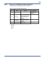
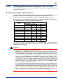
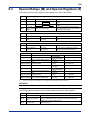
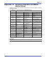
1.2.3
Configuration
This section describes the configuration function. The configuration setup ranges are
summarized in the table below.
Configuration Function
The sequence CPU contains the predefined defaults of device sizes and operation
methods.
You can use these defaults to run programs. In some applications, however, they may
not suit your specific purpose of use. In such a case flexibility allows for defaults to be
changed to meet your needs. Changing the defaults is called “configuration” and can be
performed through the FA-M3 programming tool WideField3 (hereinafter simply referred
to as WideField3) and the FA-M3 programming tool WideField2.
Tables of Configuration Ranges
Table 1.6 Configuration Range (1/5)
Device
capacities
F3SP22-0S, F3SP28-3N, F3SP28-3S, F3SP53-4H, F3SP53-4S
Item
Default
Configuration Range
2048 points max. on 32-point
Shared relay (E)
0
basis for all CPUs combined
Extended shared relay
2048 points max. on 32-point
0
(E)
basis for all CPUs combined
Shared Device (E, R)
1024 points max. on 2-point basis
Shared register (R)
0
for all CPUs combined
Extended shared
3072 points max. on 2-point basis
0
register (R)
for all CPUs combined
System 1 to 4: 2048 8192 points max. on 16-point
Link relay (L)
basis (Note) for all links combined.
System 5 to 8: 0
Link Device (L, W)
System 1 to 4: 2048 8192 points max. on 16-point
Link register (W)
basis (Note) for all links combined.
System 5 to 8: 0
100 μs timer
0
1 ms timer
0
2048 points on 1-point basis for
timers and counters combined; 16
10 ms timer
512
max. for 100 μs timers; Timer
Configuration of Timer (T) 100 ms timer
448
numbers are continuous.
/Counter (C)
100 ms continuous
128
timer
2048 points on 1-point basis for
Counter
1024
timers and counters combined.
IM 34M06P13-01E
4th Edition : Jan. 31, 2012-00
1-8
Table 1.7 Configuration Range (2/5)
F3SP38-6N, F3SP38-6S, F3SP58-6H, F3SP58-6S, F3SP59-7S
Default
Configuration Range
2048 points max. on 32-point basis for all
Shared relay (E)
0
CPUs combined
2048 points max. on 32-point basis for all
Extended shared relay (E)
0
CPUs combined
Shared Device (E, R)
1024 points max. on 2-point basis for all
Shared register (R)
0
CPUs combined
3072 points max. on 2-point basis for all
Extended shared register (R)
0
CPUs combined
2048 for each
16384 points max. on 16-point basis(Note) for
Link relay (L)
all links combined
system
Link Device (L, W)
2048 for each
16384 points max. on 16-point basis(Note) for
Link register (W)
all links combined
system
100 µs timer
0
1 ms timer
0
3072 points on 1-point basis for timers and
counters combined; 16 points max. for 100
10 ms timer
1024
Configuration of Timers
µs timers; timer numbers are continuous.
100 ms timer
896
(T)/counters (C)
100 ms continuous timer
128
3072 points on 1 point basis for timers and
Counter
1024
counters combined.
Item
Device
capacities
Table 1.8 Configuration Range (3/5)
Extended
device
configuration
F3SP22-0S, F3SP28-3N/3S, F3SP53-4H/4S, F3SP38-6N/6S, F3SP58-6H/6S, F3SP59-7S
Item
Default
Configuration Range
Internal relay (I)
I0001 to I1024
Configurable on 32-point basis; continuous
shared relay (E)
from the starting number
Non-latched type
Extended shared relay (E)
Link relay (L)
Non-latched type
Configurable on 16-point basis
Non-latched type
Configuration of the range
Configurable on 1-point basis; continuous
Timer (T)
(except for
of devices to be latched in
from the starting number
continuous timers)
case of power failure
Counter (C)
All latched
Data register (D)
All latched
Configurable on 2-point basis; continuous
Shared registers (R)
from the starting number
Non-latched type
Extended shared registers (R)
Link register (W)
Non-latched type
Configurable on 16-point basis
Note: The configuration range of each of shared relays (E) and extended shared relays (E) and shared registers (R) and
extended shared registers (R) to be latched in case of power failure is assigned numbers continuous from the
starting number. However, if the number of shared relays (E) is smaller than 2048, the last of them is followed by the
first extended shared relay (E) numbered E2049. Likewise, if the number of shared registers (R) is smaller than
1024, the last of them is followed by the first extended shared register (R) numbered R1025.
Example)
In a case where there are 1024 shared relays (E) and 2048 extended shared relays (E):
If you define the starting number as 513 and the number of units as 1024 for the range of devices to be
latched in case of power failure, then the devices that are latched include:
E513 to E1024 shared relays (E); and
E2049 to E2560 extended shared relays (E).
Note: The configuration range of each of link relays (L) and registers (W) to be latched in case of power failure is assigned
numbers continuous from the starting number.
However, the following exceptions apply.
The number following L/W01024 is L/W11024.
The number following L/W11024 is L/W21024.
The number following L/W21024 is L/W31024.
The number following L/W31024 is L/W41024.
The number following L/W41024 is L/W51024.
The number following L/W51024 is L/W61024.
The number following L/W61024 is L/W71024.
(The rules noted above are true when the number of link relays (L) or registers (W) to be used is defined as 1024.
If the number is 2048, the number following L/W02048 is L/W10001.)
Example:
When there are 1024 link relays (L) each for link 1, link 2 and link 3:
If you define the starting number as 10513 and the number of units as 1024 for the range of devices to be
latched in case of power failure, then the devices included in the latching are:
L10513 to L11024 link relays (L) for link 1; and
L20001 to L20512 link relays (L) for link 2.
IM 34M06P13-01E
4th Edition : Jan. 31, 2012-00
1-9
Table 1.9 Configuration Range (4/5)
F3SP22-0S, F3SP28-3N/3S, F3SP53-4H/4S, F3SP38-6N/6S, F3SP58-6H/6S, F3SP59-7S
Item
Default Value
Value Range
Configurable for up to 1024
Initial data of data register
Data register (D)
None
contiguous points from a starting
number
Configurable from 10 to 200 ms in
Scan monitoring time
200 ms
increments of 10 ms
Configurable from 1.0 to 190.0 ms
Constant scan
Do not Use
in increments of 0.1 ms
I/O module error
Stop
I/O comparison error
Stop
Instruction parameter
Stop
error
Error-time action
Scan timeout
Stop
(operating mode in
Run/Stop (configurable)
Subroutine error
Stop
Operation
case of error)
Interrupt error
Stop
Control
Subunit communication
Run
error
Sensor CB scan
Stop
timeout
Program execution mode
All Blocks
All Blocks/Specified Blocks
Valid for all power
Momentary power
supply modules except
Standard mode
Standard/Immediate
failure detection mode
F3PU01-0N
100 µs to 190 ms in increments of
Peripheral processing time
Not set up
100 µs
200 µs to 25.0 ms in increments of
Execution interval
200 µs
100 µs
Immediate
Sensor CB
(during
After Instruction/Immediate (during
Timing of interrupt
instruction execution)
instruction
Interrupt
execution)
Setup
After Instruction/Immediate (during
Input interrupt
Timing of interrupt
After instruction
instruction execution)
Sensor CB
Sensor CB interrupt has
Priority of interrupts
interrupt has
priority/Input module has priority
priority
Used/Not used/Use with SCB;
Terminal usage (Module used/not used)
Used
Configurable on 16-terminal basis
BIN/BCD; configurable on 16Data code
BIN
terminal basis
Input/Output
16 ms/1 ms/250 µs/62.5
Setup
Input sampling interval
16 ms
µs/Always; configurable on 16terminal basis
Output when stopped (Reset/hold external outputs
Reset/hold; configurable on 16Reset
when sequence stops)
terminal basis
Device current values
Data registers (D)
Up to 32768 contiguous points
ROM Setup
None
to be resident in ROM
File registers (B)
from a starting number
Note: Configure on 32-terminal basis when using the same input module for both sensor control block and regular blocks.
SEE ALSO
For more information on the subunit communication error, see “Fiber-optic FA-bus Module and Fiberoptic FA-bus Type 2 Module, FA-bus Type 2 Module” (IM 34M06H45-01E).
IM 34M06P13-01E
4th Edition : Jan. 31, 2012-00
1-10
Table 1.10 Configuration Range (5/5)
F3SP22-0S, F3SP28-3N/3S, F3SP53-4H/4S, F3SP38-6N/6S, F3SP58-6H/6S, F3SP59-7S
Item
Default Value
Value Range
Mode 0: 9600bps, Even Parity
Mode 1: 9600bps, No Parity
Mode 2: 19200bps, Even Parity
Mode 3: 19200bps, No Parity
Connection port for
Communication
Mode 0: 9600bps, Mode 4: 38400bps, Even Parity
programming tool
mode
even parity
Mode 5: 38400bps, No Parity
Mode 6: 57600bps, Even Parity
Communications
Mode 7: 57600bps, No Parity
Setup
Mode 8: 115200bps, Even Parity
Mode 9: 115200bps, No Parity
Used/Unused
Unused
Unused/Used
CPU personal
Checksum
No
Yes/No
computer link
End character
No
Yes/No
(Program) protection No
Yes/No
Yes/No
FA link setup (Mapping between FA link and FL-net numbers and
None
Link number from 1 to 8
slot numbers)
Slot numbers from 1 to 16
Peripheral
Peripheral process or Control
Common data refreshing mode
FL-net
process
process
Refreshing
All nodes or Some nodes;
Common data refreshing range
All nodes
Node numbers 1 to 254
Enable/Disable refreshing,
configurable separately for
shared relays(E) , shared
Shared refreshing range (partial disabling of
All refreshed
registers(R) , extended shared
refreshing)
relays (E) and extended shared
Shared
registers (R) of each CPU
Refreshing
module
Shared refreshed data
Simultaneous
Simultaneous/Non-simultaneous
Peripheral
Peripheral process/
Shared refreshing mode
process
Control process
IM 34M06P13-01E
4th Edition : Jan. 31, 2012-00
1-11
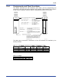
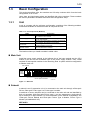
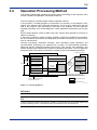
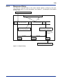
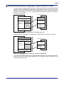
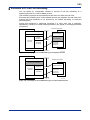
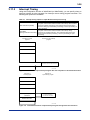
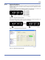
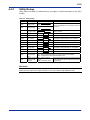
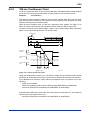
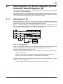
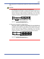
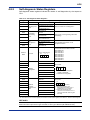
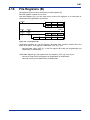
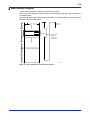
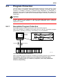
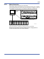
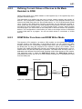
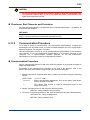
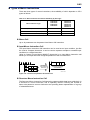
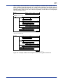
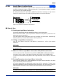
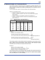
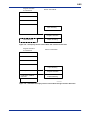
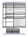
1.2.4
Components and Their Functions
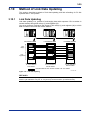
This section describes the LED indicators, their states, and the programming tool
connector on the front side of the sequence CPU module. These features are common
to the F3SP22, F3SP28, F3SP38, F3SP53, F3SP58 and F3SP59 CPU modules.
F3SP53-4H
F3SP58-6H
F3SP53-4S
F3SP58-6S
F3SP59-7S
F3SP22-0S
F3SP28-3N
F3SP38-6N
F3SP28-3S
F3SP38-6S
RDY
RUN
ALM
ERR
SP 8-0N
CPU module operation status LED indicators
R
RDY (= READY, green) ------------- On = Normal
Off = Major failure
RUN (= RUN, green)------------------ On = Program in progress
Off = Program at a stop
ALM (= ALARM, yellow)-------------- On = Minor failure
Off = Normal
ERR (= ERROR, red)----------------- On = Moderate failure
Off = Normal
CPU
SP5
PROGRAMMER
-
RDY
RUN
ALM
ERR
S
R
CPU
PROGRAMMER
Major failure -------------- The CPU module is inoperable due to a
hardware failure.
Moderate failure --------- The CPU module cannot run or continue
to run a program.
Minor failure -------------- The CPU module still can run or continue
to run a program though it has detected
a failure.
Programming tool connector
------------------ Connected to a personal computer or handy
programming console. A personal computer
or a monitor can be connected to this
connector when the personal computer link
function is in use.
F010201.VSD
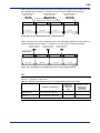
The table below summarizes combinations of the LED indicators as classified by the
severity of failure.
Table 1.11 LED Indicator Combinations Based on the Severity of Failure
Status
LED Indicator
RDY
RUN
ALM
ERR
Normal
Major
Failure
{
{
z
z
z
z
U
{
Moderate
Failure
{
z
U
{
Minor
Failure
{
{
{
z
{: ON, z: OFF, U: ON or OFF
Table 1.12 Weight
Model
F3SP22, F3SP28, F3SP38
F3SP53, F3SP58, F3SP59
Weight
130g
210g
IM 34M06P13-01E
4th Edition : Jan. 31, 2012-00
1-12
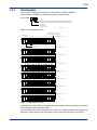
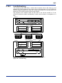
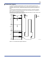
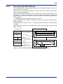
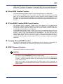
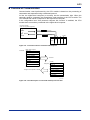
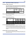
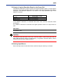
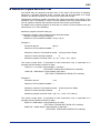
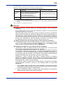
1.2.5
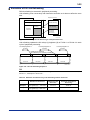
External Dimensions
Unit: mm
F3SP22
F3SP28
F3SP38
83.2
28.9
2
100
F010202.VSD
F3SP53
F3SP58
F3SP59
113.2
83.2
30.0
28.9
2
100
F010203.VSD
IM 34M06P13-01E
4th Edition : Jan. 31, 2012-00
1-13
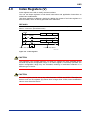
1.3
Basic Configuration
This section describes units, slot numbers and I/O relay numbers which form the basic
configuration of an FA-M3.
Units, slots, and input/output relays are identified with unique numbers. These numbers
are used in parameters of ladder instructions and configuration setup.
1.3.1
Unit
A unit is a system with the minimum configuration consisting of the following modules.
Install these modules on the base module to compose the unit.
Table 1.13 Unit Components (Modules)
Name
Base module
Power supply module
CPU module
I/O module
Special module
Description
Five types are available allowing different number
of modules to be mounted.
One power supply module must always be mounted
on the base module.
At least one CPU module is required. Several types
are available with different functionalities.
Various types are available with different types of
I/O and number of I/O points.
Various types are available, including analog I/O
and communication modules.
The location where you install a module is called a slot.
Main Unit
Install the power supply module in the leftmost slot of the base module and the CPU
module in the slot on the immediate right of the power supply module. Then, install
required I/O and special modules in the remaining slots. A system with this configuration
is called a main unit.
CPU module
Power
supply
module
I/O and special modules
F010301.VSD
Figure 1.1 Main Unit
Subunit
A subunit is an I/O expansion unit. It is connected to the main unit through a fiber-optic
FA-bus, fiber-optic FA-bus type 2 or FA-bus type 2 module.
A maximum of seven subunits can be connected to the main unit and are identified by
their unit numbers. With fiber-optic FA-bus type 2, you can separate any single subunit
into a maximum of eight stations. For more information on the method of separation, see
“Fiber-optic FA-bus Module and Fiber-optic FA-bus Type 2 Module, FA-bus Type 2
Module” (IM 34M06H45-01E).
SEE ALSO
For details on unit number, see Section 1.3.2.
IM 34M06P13-01E
4th Edition : Jan. 31, 2012-00
1-14
Slot Number
A slot number indicates the position of a slot where a module is installed.
A slot number is defined as a three-digit integer, as shown below.
Slot number
Slot positions 01 to 16 are assigned to the slot on the immediate right of
the power supply module through to the rightmost slot of a base module.
Unit number
Main unit = 0
Subunit = 1 to 7
F010302.VSD
Figure 1.2 Slot Numbers (1 of 2)
Fiber-optic FA-bus type 2 module
(can be installed in any position)
FA-M3 main unit
002 003
004 005
006 007
008
009
010 011
012 013
014
015 016
Slot numbers 001 to 016
Power supply
module
001
Add-on CPUs (three CPUs max.)
CPU module
Subunit 1
102 103
104 105
106
107
108 109
110 111
112 113
114 115
116
Slot numbers 101 to 116
201
202 203
204 205
206
207
208 209
210 211
212 213
214 215
216
Slot numbers 201 to 216
301
302 303
304 305
306
307
308 309
310 311
312 313
314 315
316
Slot numbers 301 to 316
401
402 403
404 405
406
407
408 409
410 411
412 413
414 415
416
Slot numbers 401 to 416
501
502 503
504 505
506
507
508 509
510 511
512 513
514 515
516
Slot numbers 501 to 516
601
602 603
604 605
606
607
608 609
610 611
612 613
614 615
616
Slot numbers 601 to 616
701
702
704
706
707
708
710
716
Slot numbers 701 to 716
Power supply
module
101
Power supply
module
Subunit 2
Power supply
module
Subunit 3
Power supply
module
Subunit 4
Power supply
module
Subunit 5
Power supply
module
Subunit 6
Subunit 7
703
705
709
711 712
713 714
715
Power supply
module
1.3.2
F010303.VSD
Figure 1.3 Slot Numbers (2 of 2)
Install fiber-optic FA-bus type 2 modules in both the main unit and a subunit and connect
these modules with a fiber-optic cable.
You can attach up to seven subunits to the main unit. Subunit numbers are assigned by
setting the rotary switch on the front panel of each fiber-optic FA-bus type 2 module.
IM 34M06P13-01E
4th Edition : Jan. 31, 2012-00
1-15
1.3.3
I/O Relay Number
Each input relay (X) or output relay (Y) number is defined as a slot number followed by
an I/O relay number. The I/O relay number is a number corresponding to each terminal
of an I/O module.
Example:
The output relay number for terminal 6 of an F3YC08-0N module installed in slot 005 is
defined as follows.
Y005
06
Terminal number
Slot number
001 002 003 004 005 006 007 008 009 010 011 012 013 014 015 016
Slot numbers
15
26
37
48
Y 08-
OUT
1
2
3
4
5
6
Output relay number
Y00506
7
8
COM
F3YC08-0N
F010304.VSD
Figure 1.4 Output Relay Number
The input and output terminal numbers of a mixed-I/O module or special module with 32
input and output points each are assigned as 1 to 32 and as 33 to 64, respectively.
IM 34M06P13-01E
4th Edition : Jan. 31, 2012-00
Blank Page
2-1
2.
System Configuration
This chapter describes the FA-M3 system configuration and programming tools.
2.1
Basic System Configuration
The basic system configuration refers to a system consisting of a main unit only.
For more information on the main unit, see subsection 1.3.1, “Unit.”
Sequence CPU module or BASIC CPU module
Power
supply
module
F020101.VSD
Figure 2.1 Example of Basic System Configuration (when a 13-slot base module is used)
2.2
Multi-CPU System Configuration
This section describes a multi-CPU system configuration and the handling of I/O
modules in a multi-CPU system.
2.2.1
Multi-CPU System Configuration
A multi-CPU system configuration refers to a system comprising multiple CPU modules.
A maximum of four CPU modules can be installed in the slots (slots 001 to 004) on the
main unit.
A CPU module installed in slot 001 serves as the main CPU module and CPU modules
installed in slots 002 to 004 serve as add-on CPU modules.
A maximum of four sequence CPU modules can be installed at the same time, while
only one F3BP BASIC CPU module is allowed in this system configuration.
A CPU module installed in the Nth (N = 1 to 4) slot is called the Nth CPU (module) or
CPU N.
TIP
A BASIC CPU module refers to a CPU module which is controlled by BASIC programs.
IM 34M06P13-01E
4th Edition : Jan. 31, 2012-00
2-2
Main CPU module
001
002
003
004
005
006
007
008
009
010
011
012
013
Add-on CPU modules
Slot numbers
F020201.VSD
Figure 2.2 Example of Multi-CPU System Configuration
CAUTION
Be careful not to install any CPU module in the 5th or later slot and turn on the power.
Otherwise, the memory is cleared and factory settings are restored.
IM 34M06P13-01E
4th Edition : Jan. 31, 2012-00
2-3
2.2.2
Handling I/O Modules in Multi-CPU System
Input Modules
With input modules, you can read input data through multiple CPUs. To do this,
configure the CPUs so that they share the same input sampling interval for the input
module in question. Be careful, as the sampling interval that can be set varies,
depending on the CPU type.
Output Modules and Special Modules with Y Output Relays (Y)
z Combination of F3SP22, F3SP28, F3SP38, F3SP53, F3SP58, F3SP59,
F3SP66, F3SP67, F3SP71 and F3SP76 CPU Modules
You can output data from multiple sequence CPU modules separately to the output
relays of the same output module on 16-point basis. To do this, configure the unused
output relays (Y) of the output module as “Not used” on 16-point basis. In addition, all
output relays within the same module must be configured with the same output mode
(hold or reset) in the event that sequence processing stops.
z Other Combinations of CPU Modules
You may not use the same output module with multiple CPUs. Configure all CPUs that
do not use the output module so that the output module is set to “Not Used.”
SEE ALSO
For details on modules that are not used, see Section 4.1.4.
IM 34M06P13-01E
4th Edition : Jan. 31, 2012-00
2-4
2.3
Extended System Configuration
An extended system configuration refers to a system configured by adding remote I/O
modules, a personal computer link module, an FA link module, and an FL-net module to
the basic system.
2.3.1
Remote I/O System
The remote I/O system refers to a system configured using fiber-optic FA-bus, fiber-optic
FA-bus type 2 and FA-bus type 2 modules.
The number of remote I/O points is included in the count of all I/O points.
Main unit
Fiber-optic FA-bus type 2 module
Fiber-optic cable
Subunit
Fiber-optic FA-bus type 2 module
Subunit
Fiber-optic cable, 100-m long
F020302.VSD
Figure 2.3 Example of System Using Fiber-optic FA-bus Type 2 Modules
IM 34M06P13-01E
4th Edition : Jan. 31, 2012-00
2-5
2.3.2
Personal Computer Link System
The personal computer link system refers to a system configured by connecting a
personal computer or a monitor to the main unit through a personal computer link
module. The sequence CPU module can be connected directly to a personal computer
or a monitor.
Personal computer or monitor
with PC interface
Main unit
Power
supply
module
Personal computer link module
F020303.VSD
Figure 2.4 Example of Personal Computer Link System
2.3.3
FA Link System
The FA link system refers to a system that employs FA link communication to build a
network system with programmable controllers.
The types of communication covered by an FA link system are:
- FA link H communication (FA link H module), and
- Fiber-optic FA link H communication (fiber-optic FA link H module).
Unless otherwise specified, the term “FA link” in this manual comprehensively refers to
these two types of communication. For more information on the FA link, see “FA Link H
Module, Fiber-optic FA Link H Module” (IM 34M06H43-01E).
FA link
Main unit
Main unit
Main unit
FA link H module, Fiber-optic FA link H module
F020304.VSD
Figure 2.5 Example of FA Link System
IM 34M06P13-01E
4th Edition : Jan. 31, 2012-00
2-6
2.3.4
FL-net System
An FL-net system is based on FL-net, which is an open network for connecting various
programmable controllers (PLC), computerized numerical controllers (CNC) and other
factory automation (FA) controllers (including personal computers (PC)) from multiple
vendors.
For details on FL-net, see "FL-net (OPCN-2) Interface Module" (IM 34M06H32-02E).
PC
PC
PC
EWS
SERVER
Computers
WAN
Information network (upper LAN Ethernet) (TCP/IP, UDP)
FL-net (OPCN-2) (Ethernet controller network)
FA controllers
PLC
PLC
PLC
Smart
display
CNC
RC
Field network
FA devices
Sensors and
actuators
F020305.VSD
IM 34M06P13-01E
4th Edition : Jan. 31, 2012-00
2-7
2.4
Programming Tool
The FA-M3 programming tool WideField3 and WideField2, or simply WideField3 and
WideField2, is available as a programming tool for the F3SP22, F3SP28, F3SP38,
F3SP53, F3SP58 and F3SP59 sequence CPU modules.
2.4.1
WideField3/WideField2
Description
FA- M3 Programming Tool WideField3
Description
FA- M3 Programming Tool WideField2
Software Model
SF630-CW
Software Model
SF620-MCW
Compatible Sequence CPU
Modules
F3SP05 F3SP08 F3SP21
F3SP22 F3SP25 F3SP35
F3SP28 F3SP38 F3SP53
F3SP58 F3SP59 F3FP36
F3SP66 F3SP67
F3SP71 F3SP76
Compatible Sequence CPU
Modules
F3SP05 F3SP08 F3SP21
F3SP25 F3SP35
F3SP28 F3SP38 F3SP53
F3SP58 F3SP59 F3FP36
F3SP66 F3SP67
Personal computer
F020401.VSD
Figure 2.6 WideField3
Object Ladder
WideField3 (or WideField2) defines “blocks” and “instruction macros” that compose a
ladder program as “objects,” a term commonly used in the computing world. All objects
are responsible for their provided functions and have a high degree of independence.
Consequently, the language offers higher productivity, better maintainability and more
effective program reuse, as compared to a structured programming language.
Features
z Componentization
With componentization, blocks can be reused as complete components. Devices that
are used within a block are defined separately from the main program. Thus, blocks can
be easily recombined without undesirable duplicate use of the same device. Macro
functions can also be turned into components.
.
IM 34M06P13-01E
4th Edition : Jan. 31, 2012-00
2-8
z Index View
You can display an outline view of a large program by “hiding” non-required details. This
enables more efficient debugging.
Material feed
Initialization
Idling
Initialization
Idling
Material feed
Preheating
Material feed
Preheating
Flux coating
Finish coat
Fixation heating
Cleaning
Cooling
Unloading
Preheating
Flux coating
Finish coat
Fixation heating
Cleaning
Cooling
Unloading
Fault-diagnosis
Power-off sequence
Flux coating
Fault-diagnosis
Power-off sequence
F020402.VSD
z Group Tag Names
You can group individual tag names into a group tag name to enable definition of data
sets.
SW01
POMP01
OUT01
SW02
POMP02
OUT02
SW03
POMP03
OUT03
Define
data structure
SWICH
POMP
OUT
MCN1
MCN1.SWICH
MCN1.POMP
MCN1.OUT
MCN2.SWICH
MCN2.POMP
MCN3.OUT
MCN3.SWICH
MCN3.POMP
MCN3.OUT
MCN2
Name
data sets
MCN3
F020403.VSD
z Easy Data Exchange with Windows-based Applications
You can select data items such as device names and comments on a Microsoft Excel
screen and copy them to WideField3 (or WideField2) (drag-and-drop function). You can
also copy ladder circuits created using WideField3 (or WideField2) to Windows
applications such as Microsoft Word.
IM 34M06P13-01E
4th Edition : Jan. 31, 2012-00
3-1
3.
Basic Operations of Sequence CPU
Module
This chapter describes the basic operating modes of the sequence CPU module
and add-on CPU modules, as well as their methods of program execution.
3.1
Operating Modes of Sequence CPU Module
The sequence CPU module has three operating modes: Run mode, Debug mode and
Stop mode.
Run Mode
The Run mode is a state in which the sequence CPU module is running a program, and
is used for actual system operation. You can monitor the operating status of a sequence
CPU module or devices. However, you can use none of the debug functions available
from the WideField3 (or WideField2) programming tool. In this mode, the RDY and RUN
LED indicators turn on.
Debug Mode
The Debug mode is used when debugging and tuning programs.
You can execute programs in the same way as with the Run mode. In Debug mode, you
can use debugging functions, such as forced SET/RESET instructions and online edit,
through WideField3 (or WideField2). These functions, however, affect the scan time.
Disable the functions at the end of debugging and tuning, and set the CPU to Run
mode. In this mode, the RDY and RUN LED indicators turn on.
The Debug mode includes a pause state in which the sequence CPU module suspends
program execution during such debugging operation as scan operation. In this state, the
RUN LED indicator turns off and all external outputs being generated by the program
are latched.
Stop Mode
The Stop mode is a state in which the sequence CPU module stops program execution.
In this mode, you can remove programs and clear devices, in addition to using forced
SET/RESET instructions, online editing and debug operation. In this mode, the RUN
LED indicator turns off.
The external outputs being generated by the program are set to ON (hold) or OFF
(reset), according to the setting of the configuration item "Output When Stopped" of
"Input/Output Setup." By default, all external outputs are set to OFF.
Table 3.1 LED Indicator Combinations Based on the Operating Mode
Operating Mode
LED Indicator
RDY
RUN
ALM
ERR
Run
Debug
Stop
{
{
{
U
{
z
z
z
z
z
z
z
{: ON, z: OFF, U: ON or OFF
IM 34M06P13-01E
4th Edition : Jan. 31, 2012-00
3-2
3.2
Operation at Power-on/off
This section describes the operations when power is turned off or turned on.
3.2.1
Operation at Power-on
When the power is turned on, the CPU performs initialization to get ready for program
execution.
During initialization, the CPU performs I/O collation and instruction interpretation to
check whether its hardware and programs are normal.
If no error is detected, the CPU begins executes a program from its beginning.
If equipped with a ROM pack, the CPU reads programs from the pack and begins
system operation.
If in the ROM Writer mode, however, the CPU does not read programs from the ROM
pack. Alternatively, it enters a command-wait state (e.g., waits for a ROM transfer
command from the WideField3 (or WideField2)) without executing a program.
Power-on
Self-diagnosis
Error?
NO
YES
YES
The RDY LED
indicator turns on.
ROM writer mode?
NO
NO
Equipped with
ROM pack?
YES
Read programs from
ROM pack
Program diagnosis
Error?
Wait for command
YES
NO
Start program
The RUN LED
indicator turns on.
Stop
The ERR LED
indicator turns on.
F030201.VSD
Figure 3.1 Operation at Power-on
3.2.2
Operation at Power-off
When the power is turned off, the sequence CPU module records the date and time in
its error log file and stops system operation.
TIP
The error log function saves to an error log file information such as time of occurrence and type of error
when a system error occurs or when the power is turned on or turned off.
SEE ALSO
For details on the error log, see Chapter C3 of "FA-M3 Programming Tool WideField3” (IM 34M06Q16E) or Chapter B23 of “FA-M3 Programming Tool WideField2” (IM 34M06Q15-01E).
IM 34M06P13-01E
4th Edition : Jan. 31, 2012-00
3-3
3.3
Operation in Case of Momentary or
Complete Power Failure
This section describes settings for operation in case of momentary power failure,
specifying the momentary power failure detection mode, as well as operation in case of
complete power failure, specifying the data latch range in case of complete power
failure.
3.3.1
Operation in Case of Momentary Power Failure
Two types of power failure detection mode are available for detecting a momentary
power failure: the standard mode and the immediate detection mode.
The CPU operates differently in case of a momentary power failure, depending on the
type of power failure detection mode selected.
The immediate detection mode can be selected by configuration only when the
F3PU10-0, F3PU16-0N, F3PU20-0, F3PU26-0N, F3PU30-0 or F3PU36-0 power
supply module is used.
Standard Mode
If a momentary power failure occurs, the sequence CPU module records the date and
time in its error log file. The sequence CPU module suspends processing until the power
is restored. This causes a delay in the scan time and timer update process.
When the power is restored, the sequence CPU module resumes execution at the point
where processing was suspended.
A program can detect a momentary power failure by monitoring a special relay (M195).
AC voltage
Power failure detection level
Program
execution
Interruption
F030301.VSD
Figure 3.2 Operation in Case of Momentary Power Failure
CAUTION
While the sensor control block is active, a momentary power failure may result in a
sensor control block scan timeout. In this case, the sensor control block stops and must
be restarted after the power is restored.
Immediate Detection Mode
If a momentary power failure occurs, the sequence CPU module records the date and
time in its error log file. The sequence CPU module suspends processing until power is
restored. At this point the CPU sets the external outputs generated by a program to OFF,
and actuates the FAIL contact.
When power is restored, the sequence CPU module performs a reset-and-start
sequence and executes the program from its beginning.
IM 34M06P13-01E
4th Edition : Jan. 31, 2012-00
3-4
3.3.2
Momentary Power Failure Detection Mode Setup
This configuration item defines the momentary power failure detection mode.
You can select either the standard mode or the immediate detection mode. The default
is the standard mode. For details on each of these modes, see "Hardware Manual" (IM
34M06C11-01E).
CAUTION
In a multi-CPU configuration, all CPU modules must be configured with the same
momentary power failure detection mode.
3.3.3
Operation in Case of Complete Power Failure
If a complete power failure occurs, the CPU operates as it does at power off.
You can configure the types and ranges of devices to be latched in case of a complete
power failure. This strategy allows the CPU to resume operation from its previous state
after power is restored.
When power is restored, the CPU executes the program from its beginning.
TIP
Latching devices at power failure stores device states immediately before a power failure so that a
program can continue execution in the same state after power is restored.
3.3.4
Data Latch Range at Power Failure
This configuration item sets the range of devices to be latched in case of a complete
power failure.
Specify the starting number and the number of devices for each device type.
The following table shows the default setting and the configurable range of each device
type.
Table 3.2 Data Latch Range at Power Failure of Configuration
Item
Internal relay (I)
Shared relay (E)
Extended shared relay (E)
Link relay (L)
Timer (T)
Data Latch
Extended
Range at
device
Power
Counter (C)
configuration
Failure
Data register (D)
F3SP22
F3SP28
F3SP53
I0001 to I1024
Default
F3SP38
F3SP58
F3SP59
Configuration Range
I0001 to I1024
I0001 to I1024
Non-latching type
Non-latching type
Non-latching type
Non-latching type
Non-latching type
Non-latching type
Non-latching type
(except for
continuous timers)
All latched
(C0001 to C1024)
All latched
(D00001 to
D16384)
Non-latching type
(except for
continuous timers)
All latched
(C0001 to C1024)
All latched
(D00001 to
D32768)
Non-latching type
(except for
continuous timers)
All latched
(C0001 to C1024)
All latched
(D00001 to
D65535)
Configurable on 32-relay
basis; contiguous from a
starting number*1
Configurable on 16-relay
basis*2
Non-latching type
Non-latching type
Non-latching type
Non-latching type
Shared register (R)
Non-latching type
Extended shared register (R)
Link register (W)
*1:
*2:
Non-latching type
Configurable for
timers/counters, contiguous
from a starting number
Configurable on 2-register
basis; contiguous from a
starting number*1, *2
Configurable on 16-register
basis*2
If the upper limit of the range of shared relays (E) used is smaller than E2049, the last device number for shared
relays (E) is followed by the first device number for extended shared relays (E). Likewise, if the upper limit of shared
registers (R) used is smaller than R1025, the last device number for shared registers (R) is followed by the first
device number for extended shared registers (R).
The data latch range setup for link relay and link register are mapped to contiguous devices starting from their
respective starting numbers with the following exceptions:
L/W01024 is followed by L/W10001;
L/W11024 is followed by L/W20001;
L/W21024 is followed by L/W30001;
L/W31024 is followed by L/W40001;
L/W41024 is followed by L/W50001;
L/W51024 is followed by L/W60001;
L/W61024 is followed by L/W70001.
The above rule applies when the number of link relays or registers to be used is defined as 1024.
If the number used is 2048, L/Wn2048 is followed by L/Wn0001. If the number used is 8192, L/W08192 is followed
by L/W10001.
IM 34M06P13-01E
4th Edition : Jan. 31, 2012-00
3-5
3.4
Operation Processing Method
This section outlines data operation processing (scan processing) in the sequence CPU
module. Details are explained in subsequent sections.
The CPU employs a stored-program iterative operation method.
In this method, a created program is pre-stored in the memory of the sequence CPU
module. The sequence CPU executes instructions, one at a time, starting from the first
step of the program. After executing the last step in the program, the CPU performs
required processing, such as self-diagnosis. It then repeats the instructions from the first
step.
Each of these iterative cycles is called “one scan” and the time required for one scan is
called a “scan time.”
In the case of F3SP22, F3SP28, F3SP38, F3SP53, F3SP58 and F3SP59 CPU modules,
the CPU executes instructions and peripheral processes concurrently to perform each
scan in a shorter time.
Common processing, instruction execution, input refreshing, output refreshing, and
synchronization processing are classified as a system of control-related processes,
while tool service, personal computer link service, CPU service, link refreshing, and
shared refreshing are classified as a system of peripheral processes. The CPU performs
these two kinds of processes concurrently to speed up the control-related processes.
Peripheral processes
Input refreshing for
sensor control block
Fixed
interval of
200 s
or longer
Program execution for
sensor control block
Output refreshing for
sensor control block
Common processing
Output
refreshing
One scan
Input refreshing for
sensor control block
Program execution for
sensor control block
Output refreshing for
sensor control block
Shared
refreshing
Input refreshing
Instruction
execution
Peripheral
processes
are performed
within this
time range.
Execution interrupt
Link refreshing
Command
processing
- Tool service
- Link service
- CPU service
Synchronization processing
If synchronization processing begins,
any peripheral process is interrupted
temporarily and resumes at the next scan.
Shows a case when the sensor
control function is used.
Control-related process
Peripheral process
F030401.VSD
Figure 3.3 Processing Method
SEE ALSO
For details on the sensor control function, see Section 6.15, “Sensor Control Function.”
TIP
Common processing includes self-diagnosis, updating of special relays (M) and special registers (Z),
as well as updating of timers. The END processing is sometimes known as an END scan.
IM 34M06P13-01E
4th Edition : Jan. 31, 2012-00
3-6
TIP
The input refreshing process reflects data from input contacts of, say a DI module, to input relays (X).
The output refreshing process reflects data from output relays (Y) to output contacts of, say a DO
module.
TIP
The synchronization process synchronizes the system of control-related processes with the system of
peripheral processes. In particular, it reflects data to the link refresh and shared refresh (inter-PLC
communication) devices.
z System of Control-related Processes
This system performs basic operations of the sequence CPU module, such as
instruction execution and I/O refreshing.
Execution of the system of control-related processes is called one scan, and the
execution time required by the system is usually called the scan time.
z System of Peripheral Processes
This system supports the programming tool WideField3 and performs communication
between the CPU module and a personal computer or an FA link module.
The system of peripheral processes is concurrent with and independent of the system of
control-related processes. Therefore, neither the number of modules connected nor the
content of each peripheral process affects the operation of the system of control-related
processes.
z Synchronization between Systems of Control-related Processes and
Peripheral Processes
The system of peripheral processes executes concurrent with and independent of the
system of control-related processes. For processes related to operation control (e.g., run
or stop) or processes requiring simultaneity of data, however, the CPU synchronizes
these two systems using a synchronization process included in the system of controlrelated processes.
The time required for the synchronization process varies depending on its content.
Using debugging functions, such as online editing, affects the scan time.
CAUTION
If the ratio of the instruction execution time to the scan time is too small, insufficient time
may be allocated for executing the system of peripheral processes. Consequently, the
responses of link refreshing, shared refreshing, tool service, personal computer link
service and CPU service will become extremely slow. If this happens, use a constant
scan with an interval somewhat longer than the normal scan time, or set up the
peripheral processing time to secure sufficient time for executing the system of
peripheral processes.
IM 34M06P13-01E
4th Edition : Jan. 31, 2012-00
3-7
3.5
Method of Executing Peripheral Processes
Peripheral processes are executed concurrently with instructions in a program.
When the execution of program instructions is completed, any peripheral process is
interrupted until the next scan, in order to prevent the process from affecting the scan
time. This means the peripheral processing time is affected by the program execution
time.
Peripheral processes
Common processing
Shared refreshing
Input refreshing
Output
refreshing
Instruction
execution
Link refreshing
One scan
Command processing
- Tool service
- Link service
- CPU service
Peripheral
processing
Synchronization processing
F030501.VSD
Figure 3.4 Peripheral Processing
Specifying Peripheral Processing Time
You can define the peripheral processing time. Use this configuration item when the
instruction execution time is so short that insufficient time is allocated to peripheral
processes. To secure enough time, the scan time is lengthened, or the delays of shared
refreshing, link refreshing and command processing included in the peripheral
processes are shortened. If at the end of instruction execution, any peripheral process is
found to have not run as long as the defined time, the process is prolonged until the
expiry of the defined time. In that case, the scan is also prolonged by as much as the
extended portion of the defined time. Beware that the CPU ignores the defined
peripheral processing time if a constant scan time is defined.
Common processing
Input refreshing
Output
refreshing
Instruction
execution
Peripheral
processing
Peripheral
processing time
Wait
Synchronization processing
F030502.VSD
Figure 3.5 Peripheral Processing Time
The configurable range is from 0.1 ms to 190 ms, on 0.1 ms basis. If no peripheral
processing time is defined, the CPU operates with a peripheral processing time of 0.2
ms by default.
IM 34M06P13-01E
4th Edition : Jan. 31, 2012-00
3-8
3.6
Method of I/O Processing
This section describes how I/O processing is performed, I/O response delay, as well as
I/O processing in a multi-CPU system.
3.6.1
Method of I/O Processing
As the method of I/O processing, the CPU uses batch refreshing.
In this method, the sequence CPU module acquires all data changes in the input module
into the input relay (X) area of the CPU’s data memory before executing each scan.
The sequence CPU module uses data contained in this area when performing
operations.
Operation results are output to the output relay (Y) area of the CPU’s data memory each
time an operation is performed. The results are sent to the output module, collectively
and concurrently with the execution of instructions in the next scan.
Only modules that are installed in the system and configured in Input/Output Setup as
"Used" will have their input and output refreshed. No error occurs even if a program tries
to access input or output relays of a module which is not installed or a module which is
configured in Input/Output Setup as "Not used".
External input
instrument
Input refreshing
CPU's data memory
Input-relay (X) area
Execution of operations
X00502
Y00602
X00501
X00502
Y00601
X00503
I0001
Y00603
I0002
L0001
Y00604
I0100
CPU's data memory
Operation
results
Output-relay (Y) area
External output
instrument
Output refreshing
F030601.VSD
Figure 3.6 Method of I/O Processing
IM 34M06P13-01E
4th Edition : Jan. 31, 2012-00
3-9
3.6.2
Response Delay
The maximum response delay of the output module against a change in the input
module is two scans. For more information, see Chapter 7, “I/O Response Time Based
on Scan Time”.
External input instrument is turned on
X00502
Y00602
“ON”
“ON”
Instruction execution
The change is acquired at this
moment of input refreshing.
Instruction execution
The change is reflected at this
moment of output refreshing.
Response delay of
two scans
One scan
One scan
Output
External output instrument turns on.
F030602.VSD
Figure 3.7 Response Delay
IM 34M06P13-01E
4th Edition : Jan. 31, 2012-00
3-10
3.6.3
I/O Processing in Multi-CPU System
The sequence CPU module performs refreshing when the configuration item “Terminal
Usage” of “Input/Output Setup” is set to “Used” or “Use with SCB.”
In the configuration, define the terminals to be refreshed for each sequence CPU
module. Each sequence CPU module refreshes the terminals independently according
to the definition.
Be careful not to configure the CPUs so that more than one CPU refreshes the same
terminal of the output module. Otherwise, the resultant output of the output module will
be indefinite.
SEE ALSO
For details on the parameters set for I/O modules and their limitation of use, see Subsection 2.2.2,
“Handling I/O Modules in Multi-CPU System” and subsection 4.1.4, “Configuring DIO Modules.”
Main CPU module (sequence CPU or BASIC CPU module)
Power
supply
module
001
002
003
004
005
006
007
008
009
010
011
012
013
Add-on CPU modules
(sequence CPU or BASIC CPU modules)
Slot numbers
F030603.VSD
Figure 3.8 Example of Multi-CPU System
IM 34M06P13-01E
4th Edition : Jan. 31, 2012-00
3-11
3.7
Method of Executing Commands from
WideField3
Commands from WideField3 (or WideField2) are executed by the tool service. These
commands include downloading and uploading of programs, as well as monitoring of
devices.
3.7.1
Tool Service
The tool service executes commands sent from the FA-M3 programming tool
WideField3 or WideField2.
Since the tool service runs concurrently to the execution of instructions, it does not affect
the scan time.
The CPU does not execute the tool service if there is no command to be processed.
Monitor display
Personal computer
X00503
X00504
Y00602
X00501
X00502
Y00601
X00503
Upload
Download
Sequence CPU
Peripheral processes
Common processing
Input refreshing
Output
refreshing
Instruction
execution
Shared refreshing
Link refreshing
Command processing
- Tool service
- Link service
- CPU service
Synchronization processing
F030701.VSD
Figure 3.9 Execution of Commands Sent from the WideField3/WideField2
IM 34M06P13-01E
4th Edition : Jan. 31, 2012-00
3-12
3.8
Method of Executing Commands through
Personal Computer Link
The CPU uses the personal computer link service to execute commands sent through
the personal computer link. These commands include downloading and uploading
programs and reading from and writing to devices.
3.8.1
Personal Computer Link Service
The personal computer link service executes commands sent from a personal computer
or a monitor connected to the personal computer link module.
Since the personal computer link service runs concurrently to the execution of
instructions, it does not affect the scan time.
The CPU does not execute the personal computer link service if there is no command to
be processed.
Personal computer
or monitor
Personal computer link
Sequence CPU
Peripheral processes
Common processing
Shared refreshing
Input refreshing
Output
refreshing
Instruction
execution
Link refreshing
Command processing
- Tool service
- Link service
- CPU service
Synchronization processing
F030801.VSD
Figure 3.10 Execution of Commands through Personal Computer Link
IM 34M06P13-01E
4th Edition : Jan. 31, 2012-00
3-13
3.9
Method of CPU-to-CPU Data
Communication
CPU-to-CPU communication in a multi-CPU system configured using add-on CPUs is
carried out using a shared data communication method and CPU services.
Communications between sequence CPU modules is carried out using shared data
communications, while communications between sequence CPU modules and other
types of CPU modules, such as BASIC CPU modules, is carried out using shared data
communications or CPU services.
This section describes methods for updating shared data, configuration of shared
refreshing and the CPU service.
3.9.1
Method of Updating Shared Data
CPU-to-CPU data exchange in a multi-CPU system configured using multiple CPU
modules is carried out through shared relays (E), extended shared relays (E), shared
registers (R) and extended shared registers (R). Hereafter, shared relays (E), extended
shared relays (E), shared registers (R) and extended shared registers (R) are
collectively referred to as shared devices.
You must configure in advance the range of shared devices to be used for each installed
CPU module. The configuration of a CPU module must tally with the configuration of the
other CPU modules. You can both read from and write to shared devices within a CPU
module’s own area. However, you can only read from shared devices within the areas of
the other CPU modules.
SLOT1
SLOT2
SLOT3
SLOT4
CPU1
CPU2
CPU3
CPU4
Shared-register
area
Shared-register
area
Shared-register
area
Shared-register
area
Read/write
CPU1 area
Read
CPU2 area
Read
CPU3 area
Read
CPU4 area
Read/write-enabled area
Read-only area
F030901.VSD
Figure 3.11 Example of Configuring Shared Registers (R)
IM 34M06P13-01E
4th Edition : Jan. 31, 2012-00
3-14
The figure below shows an example of shared refreshing carried out between a
sequence CPU module and an add-on CPU module. In this example, shared relays (E)
and shared registers (R) are allocated as shown below.
- Sequence CPU module:
Shared relays (E)= E0001 to E0512
(Slot1 CPU)
Shared registers (R) = R0001 to R0256
- Add-on CPU module:
Shared relays (E)= E0513 to E1024
(Slot2 CPU)
Shared registers (R) = R0257 to R0512
SLOT1 CPU
X00502
MOV
X00501
$100
E00513
R0001
E0001
Slot-1 shared-relay area
Slot-2 shared-relay area
Slot-1 shared-register area
Slot-2 shared-register area
Shared refreshing
SLOT2 CPU
Slot-1 shared-relay area
Slot-2 shared-relay area
Slot-1 shared-register area
Slot-2 shared-register area
E0001
X00604
MOV
X00601
T001
R0001
D0001
E0513
X00603
F030902.VSD
Figure 3.12 Shared Refreshing
IM 34M06P13-01E
4th Edition : Jan. 31, 2012-00
3-15
3.9.2
Configuration of Shared Refreshing
This subsection describes the shared refreshing range (partial disabling of refreshing),
simultaneity of shared refreshed data, and shared refreshing mode (changing to controlrelated process).
Shared Refreshing Range (Partial Disabling of Refreshing)
Using configuration, you can disable shared refreshing for selected device types of
shared relay (E), extended shared relay (E), shared register (R) and extended shared
register (R) of each CPU module. Disabling shared refreshing between CPU modules
that do not need to exchange data shortens the overall shared refreshing interval.
SLOT1
SLOT2
SLOT3
SLOT4
CPU1
CPU2
CPU3
CPU4
Shared-register
area
Shared-register
area
Shared-register
area
Shared-register
area
Read/write
Read
Read
Read
CPU1 area
Read
Read/write
Stop Read
Stop Read
CPU2 area
Read
Stop Read
Read/write
Stop Read
CPU3 area
Read
Stop Read
Stop Read
Read/write
CPU4 area
Area whose data is used by each CPU
F030903.VSD
Figure 3.13 Example of Shared Refreshing Configuration
In the example shown in the figure above, if data need not be shared among add-on
CPU modules, the refreshing intervals of CPU2, CPU3 and CPU4 are shortened if
“CPU3 and CPU4,” “CPU2 and CPU4” and “CPU2 and CPU3” respectively are excluded
from shared refreshing.
TIP
If you exclude a CPU module from shared refreshing, its scan time shortens because data updating
done by its synchronization process is disabled. However, this prohibits sharing of data in all areas of
the other CPU modules.
Simultaneity of Shared Refreshed Data
You can specify by configuration whether to maintain simultaneity of shared refreshed
data. If you select “Simultaneous” for this configuration item when a sequence CPU
module (F3SP22, F3SP28, F3SP38, F3SP53, F3SP58, F3SP59, F3SP66, F3SP67,
F3SP71 or F3SP76 module) is combined with any number of F3SP22, F3SP28,
F3SP38, F3SP53, FS3P58, F3SP59 F3SP66, F3SP67, F3SP71 and F3SP76 modules
defined as add-on CPU modules, simultaneity of shared refreshed data is guaranteed by
the unit of shared devices (shared relays (E) and registers (R), or extended shared
relays (E) and registers (R)) being refreshed.
If anyone of the F3SP22, F3SP28, F3SP38, F3SP53, F3SP58 and F3SP59 modules is
combined with any of the F3SP21, F3SP25, F3SP35 and F3BP modules,
simultaneity of data is not guaranteed irrespective of the configuration settings.
The “Non-simultaneous” option of this configuration item is intended for compatibility
with the F3SP21, F3SP25 and F3SP35 modules. Select this option when replacing
these modules with the F3SP22, F3SP28, F3SP38, F3SP53, F3SP58 or F3SP59
modules.
IM 34M06P13-01E
4th Edition : Jan. 31, 2012-00
3-16
Shared Refreshing Mode (Changing to Control-related Process)
You can change by configuration the mode of shared refreshing, which updates the data
of relays (E) and registers (R) shared with other CPUs, so that it runs as a controlrelated process. Run shared refreshing as a peripheral process if a short scan time is
important. Alternatively, run it as a control-related process if the speed of exchanging
shared data is important.
Peripheral processes
Common processing
Shared refreshing
Input refreshing
Output
refreshing
Link refreshing
One scan
Instruction
execution
Command processing
- Tool service
- Link service
- CPU service
Synchronization processing
F030904.VSD
Figure 3.14 Executing Shared Refreshing as a Peripheral Process
Executing shared refreshing as a peripheral process reduces its effects on scanning.
Common processing
Peripheral processes
Input refreshing
(including shared refreshing)
Output
refreshing
Instruction
execution
Link refreshing
One scan
Command processing
- Tool service
- Link service
- CPU service
Synchronization processing
F030905.VSD
Figure 3.15 Executing Shared Refreshing as a Control-related Process
If you execute shared refreshing as a control-related process, the scan time lengthens.
However, this ensures that shared refreshing is not affected by link refreshing or the
command processing time.
IM 34M06P13-01E
4th Edition : Jan. 31, 2012-00
3-17
TIP
- Sequence of Shared Refreshing
For a main CPU, shared refreshing is executed in the order of CPU2’s shared relays(E)/registers(R),
CPU2’s extended shared relays(E)/registers(R), CPU3’s shared relays(E)/registers(R), CPU3’s
extended shared relays(E)/registers(R), CPU4’s shared relays(E)/registers(R), and CPU4’s extended
shared relays(E)/registers(R).
- When the configuration item “Shared Refreshing Execution” is set to “Peripheral Process”
Each single scan of peripheral processing refreshes CPU N’s shared relays(E)/registers(R) or
extended shared relays(E) /registers(R). The data that has been read is reflected in device areas
during the synchronization process occurring after the completion of shared refreshing. Note
however that if the configuration item “Shared Refreshing Data” is set to “Simultaneous,” refreshing
may be delayed by as much as three scans of peripheral processing due to the need for
synchronization with the CPU N.
- When the configuration item “Shared Refreshing Execution” is set to “Control Process”
Each single scan of control-related processing refreshes the CPU N’s shared relays(E)/registers(R)
or extended shared relays(E)/registers(R). Note however that when the configuration item “Shared
Refreshing Data” is set to “Simultaneous,” refreshing may be delayed by as much as three scans
due to the need for synchronization with the CPU N.
- Reference to a CPU’s Own Write Area
You can read data in a CPU’s write area from other CPUs. That is, you can read the data alternately
from shared relays(E)/registers(R) and from extended shared relays(E)/registers(R) in that area
during the synchronization process of each scan. Note however that when the configuration item
“Shared Refreshing Data” is set to “Simultaneous” for any of the other CPUs, refreshing may be
delayed by as much as the longest of those CPUs’ scans due to the need for synchronization with
the slowest CPU.
CPU2
Shared refreshing of
shared relays/registers
CPU2
Shared refreshing of extended
shared relays/registers
CPU3
Shared refreshing of
shared relays/registers
Data updates
are reflected
by this common
processing
Instruction execution
Instruction execution
Refreshing may be
delayed by three
scans of peripheral
processing to ensure
simultaneity of data
Instruction execution
Instruction execution
With this common processing, it becomes possible to alternately refer to the
shared relays/registers and extended shared relays/registers of a CPU from the
other CPUs. (Refreshing may be delayed by as much as the longest scan
amongst these CPUs to ensure simultaneity of data.)
One scan
One scan
One scan
One scan
F030906.VSD
Figure 3.16 Shared Refreshing as a Peripheral Process
CPU2
Shared refreshing of
shared relays/registers
CPU2
Shared refreshing of
extended shared
relays/registers
Refreshing may be delayed
by three scans of
peripheral processing to
ensure simultaneity of data
CPU3
Shared refreshing of
shared relays/registers
Instruction execution
Instruction execution
Instruction execution
Data updates are
reflected by this
common processing
Instruction execution
With this common processing, it becomes possible to alternately refer to the
shared relays/registers and extended shared relays/registers of a CPU from the
other CPUs. (Refreshing may be delayed by as much as the longest scan
amongst these CPUs to ensure simultaneity of data.)
One scan
One scan
One scan
One scan
F030907.VSD
Figure 3.17 Shared Refreshing as a Control-related Process
IM 34M06P13-01E
4th Edition : Jan. 31, 2012-00
3-18
SEE ALSO
Tables 3.3 and 3.4 show examples of how shared refreshing affects the scan time. For more
information, see Section 7.1, “Description of Scan Time.”
These examples assume that both CPU1 and CPU2 have 512 shared relays and 512 shared registers.
Table 3.3 Durations of Interference with the Scan Time by Shared Refreshing Running as a
Peripheral Process
Other Sequence
CPU Module
F3SP22/28/38/53/58
/59
F3SP21/25/35
0.916ms
1.138ms
1.138ms
Duration of
Interference with
Scan Time of
Peripheral
Processing
(=Duration of
Shared Refreshing)
0.916ms
3.908ms
1.138ms
1.138ms
3.908ms
Duration of
Shared
Refreshing
Duration of
Duration of
Interference with Scan
Synchronization
Time (= Duration of
Processing
Synchronization
Processing)
Table 3.4 Durations of Interference with the Scan Time by Shared Refreshing Running as a
Control-related Process
Other Sequence
CPU Module
F3SP22/28/38/53/58
/59
F3SP21/25/35
Duration of
Shared
Refreshing
Duration of
Synchronization
Processing
0.916ms
0.866ms
Duration of
Interference with
Scan Time
(= Duration of
Extended Shared
Refreshing plus
Duration of Shared
Refreshing)
1.782ms
3.908ms
0.866ms
4.774ms
IM 34M06P13-01E
Duration of
Interference with
Scan Time of
Peripheral
Processing
0ms
0ms
4th Edition : Jan. 31, 2012-00
3-19
3.9.3
CPU Service
CPU service exchanges data and process commands between the sequence CPU and
a BASIC CPU.
CPU service is processed concurrently with instruction execution so it does not affect
the scan time. The sequence CPU does not execute the CPU service unless it receives
a command (ENTER, OUTPUT, etc.) to be processed from a BASIC CPU.
BASIC CPU module
Sequence CPU
Peripheral processes
Common processing
Input refreshing
Output
refreshing
Instruction
execution
Shared refreshing
Link refreshing
Command processing
- Tool service
- Link service
- CPU service
Synchronization processing
F030908.VSD
Figure 3.18 CPU Service
IM 34M06P13-01E
4th Edition : Jan. 31, 2012-00
3-20
3.10
Method of Link Data Updating
This section describes methods of link data updating and link refreshing for FA link
systems and FL-net systems.
3.10.1
Link Data Updating
Link data updating is a process of exchanging data with sequence CPU modules in
remote stations through link relays (L) and registers (W).
You must configure in advance the ranges of link relays (L) and registers (W) to which
data is written in the local and remote stations.
F3LP/F3LX
F3LP/F3LX
F3LP/F3LX
FA link module or
FL-net module in
remote station
FA link module or
FL-net module in
remote station
Link
relays
Link
registers
FA link module or
FL-net module in
local station
Data allocated to each FA link module or FL-net module
F031001.VSD
Figure 3.19 Link Data Updating
SEE ALSO
For details on link data updating and link refreshing, see “FA Link H Module, Fiber-optic FA Link H
Modules” (IM 34M06H43-01E) and “FL-net (OPCN-2) Interface Module” (IM 34M06H32-02E).
IM 34M06P13-01E
4th Edition : Jan. 31, 2012-00
3-21
3.10.2
Link Refreshing
Link refreshing reads data from or writes data to devices such as link relays (L) and
registers (W) of the sequence CPU module via an FA link module or FL-net (OPCN-2)
interface module installed in the local unit. It maps the link data in the storage area of the
sequence CPU module to those of the FA link module.
The sequence CPU module reads the link data of the FA link module or FL-net
(OPCN-2) interface module automatically so data communication is transparent to a
user.
Station 1
X00502
MOV
X00501
L00033
$100
W00001
L00001
Station-1 link-relay area
Station-n link-relay area
Station-1 link-register area
Station-n link-register area
Link refreshing
Station 1
Station n
Link refreshing
Station n
Station-1 link-relay area
Station-n link-relay area
Station-1 link-register area
Station-n link-register area
L00003
X00604
MOV
X00601
L00001
W00001 D0001
L00033
X00603
F031002.VSD
Figure 3.20 Link Refreshing
IM 34M06P13-01E
4th Edition : Jan. 31, 2012-00
3-22
Execution of FA Link Refreshing
FA link refreshing is executed in peripheral processing.
Link refreshing runs concurrently with instruction execution so it does not affect the scan
time.
Peripheral processes
Common processing
Shared refreshing
Input refreshing
Output
refreshing
One scan
Instruction
execution
Link refreshing
Command processing
- Tool service
- Link service
- CPU service
Synchronization processing
F031003.VSD
Figure 3.21 Executing FA Link Refreshing as a Peripheral Process
Link refreshing updates the link relays (L)/registers (W) of FA link 1 to FA link 8 in each
cycle of peripheral processing.
Link relays/registers of
FA link 1
Link relays/registers of
FA link 2
Link relays/registers of
FA link 3
Results of link refreshing
are reflected by this common processing.
Instruction execution
One scan
Instruction execution
Instruction execution
One scan
Instruction execution
One scan
One scan
F031004.VSD
Figure 3.22 FA Link Refreshing Sequence
TIP
Table 3.5 shows an example of how link refreshing affects the scan time. For more information, see
Section 7.1, “Description of Scan Time.”
Table 3.5 Durations of Interference by Link Refreshing with the Scan Time
Number of Link Devices
Example 1
Example 2
Link relay (L) = 1024 units
Link register (W) = 1024 units
Link relay (L) = 2048 units
Link register (W) = 2048 units
Duration of
Interference with
Scan Time
Duration of Interference with
Scan Time of Peripheral
Processing
3.314 ms
16.38 ms
6.578 ms
32.7 ms
IM 34M06P13-01E
4th Edition : Jan. 31, 2012-00
3-23
Execution of FL-net Link Refreshing
You can specify by configuration whether to execute FL-net link refreshing as a
peripheral process or a control-related process.
Link refreshing executed as a peripheral process does not affect the scan time.
Executing link refreshing as a control-related process may lengthen the scan time but it
ensures that link refreshing is not affected by the shared refreshing or command
processing time.
Include link refreshing in peripheral processes if a short scan time is important.
Alternatively, include it in control-related processes if the speed of exchanging link data
is important.
Peripheral processes
Common processing
Shared refreshing
Input refreshing
Output
refreshing
Instruction
execution
Link refreshing
One scan
Command processing
- Tool service
- Link service
- CPU service
Peripheral
processing
Synchronization processing
F031005.VSD
Figure 3.23 Executing FL-net Link Refreshing as a Peripheral Process
Common processing
Peripheral processes
Input refreshing
(including link refreshing)
Output
refreshing
Instruction
execution
Peripheral
processing
Shared refreshing
One scan
Command processing
- Tool service
- Link service
- CPU service
Synchronization processing
F031006.VSD
Figure 3.24 Executing FL-net Link Refreshing as a Control-related Process
IM 34M06P13-01E
4th Edition : Jan. 31, 2012-00
3-24
When executed as a peripheral process, link refreshing updates the link relays (L) and
link registers (W) of system 1 or system 2 in each cycle of peripheral processing.
Link relays/registers of
Link relays/registers of
Link relays/registers of
System 1 (FL-net1)
System 2 (FL-net2)
System 1 (FL-net1)
Results of link refreshing
are reflected by this common processing.
Instruction execution
Instruction execution
One scan
One scan
Instruction execution
Instruction execution
One scan
One scan
F031007.VSD
Figure 3.25 FL-net Link Refreshing as a Peripheral Process
When executed as a control-related process, link refreshing updates the link relays (L)
and link registers (W) of system 1 or system 2 in each cycle of control processing.
Link relays/registers of
System 1 (FL-net1)
Link relays/registers of
System 2 (FL-net2)
Link relays/registers of
System 1 (FL-net1)
Results of link refreshing
are reflected by this
common processing.
Instruction execution
Instruction execution
One scan
One scan
Instruction execution
One scan
Instruction execution
One scan
F031008.VSD
Figure 3.26 Executing FL-net Link Refreshing as a Control-related Process
TIP
Table 3.6 shows an example of how link refreshing affects the scan time. For more information, see
Section 7.1, "Description of Scan Time."
Table 3.6 Durations of Interference by FL-net Link Refreshing with the Scan Time
Number of Link Devices
Refreshing as controlrelated process
Refreshing as peripheral
process
Link relay (L) = 8192 units
Link register (W) = 8192 units
Link relay (L) = 8192 units
Link register (W) = 8192 units
Duration of
Interference
with Scan
Time
Duration of
Interference with
Scan Time of
Peripheral
Processing
4.652 ms
0 ms
3.782 ms
4.652 ms
IM 34M06P13-01E
4th Edition : Jan. 31, 2012-00
3-25
Inter-mixing FA Link Modules and FL-net Interface Modules
Where FA link and FL-net are intermixed in a system configuration, FA link refreshing
and FL-net link refreshing are executed independently of each other.
If FL-net link refreshing is configured as a peripheral process, FA link refreshing and
FL-net link refreshing are executed in each cycle of peripheral processing.
System 2 (FA link)
link refreshing
System 1 (FL-net)
link refreshing
System 3 (FA link)
link refreshing
System 1 (FL-net)
link refreshing
System 2 (FA link)
link refreshing
Results of link refreshing
are reflected by this
common processing.
Instruction execution
One scan
Instruction execution
Instruction execution
One scan
One scan
Instruction execution
One scan
F031009.VSD
Figure 3.27 Intermixing FA Link and FL-net
Even if FL-net link refreshing is configured as a control-related process, FA link
refreshing always remains executed as a peripheral process.
IM 34M06P13-01E
4th Edition : Jan. 31, 2012-00
3-26
3.11
Method of Input Interrupt Processing
This section describes input interrupt processing, input interrupt processing control,
interrupt timing, and priority of interrupts.
3.11.1
Input Interrupt Processing
The sequence CPU module executes an input interrupt program when it detects the
rising edge of an interrupt input from an input module.
You can register a maximum of four input interrupt programs with the sequence CPU
module using input interrupt instructions (INTP instructions.)
The module can accept a maximum of eight concurrent interrupts. Input interrupt
programs are executed in the order of occurrence of their interrupt factors. If any
interrupt factor occurs during execution of an input interrupt program, the factor is
processed when the input interrupt program completes execution.
Interrupt factor 1
Interrupt factor 2
Interrupt program 1
Executed when interrupt
program 1 finishes.
Interrupt program 2
Interval of waiting for completion
of interrupt program 1.
F031101.VSD
Figure 3.28 Input Interrupt Processing
CAUTION
-
Do not register an input interrupt program for an input module with two or more CPU
modules. Otherwise, input interrupt processing may fail to be executed.
Do not use a TIMER instruction in any input interrupt program because the
instruction may not work correctly.
IM 34M06P13-01E
4th Edition : Jan. 31, 2012-00
3-27
3.11.2
Input Interrupt Processing Control
You can control the execution of input interrupt programs by means of programming.
Use the Enable Interrupt (EI) instruction and Disable Interrupt (DI) instructions
respectively to specify whether to execute (enable) or not execute (disable) an interrupt.
Interrupts are enabled by default.
An interrupt that is disabled by a DI instruction continues to be detected by the
sequence CPU but its input interrupt program is not executed. Such interrupts are
processed in order of their occurrence if and after they are enabled by an EI instruction.
A maximum of eight concurrent interrupts are accepted. The ninth or subsequent
concurrent interrupt generates an interrupt error.
Y00602
I0001
Occurrence of
interrupt
No interrupt programs
are executed in this
interval.
DI
X00503
I0002
Y00603
X00501
X00502
I0004
I0003
EI
INTP
X00301
IRET
F031102.VSD
Figure 3.29 Input Interrupt Processing Control
IM 34M06P13-01E
4th Edition : Jan. 31, 2012-00
3-28
3.11.3
Interrupt Timing
Using the configuration function of WideField3 (or WideField2), you can specify when an
interrupt program is to be executed if an interrupt occurs during program execution. The
following two options are available.
Table 3.7 Interrupt Timing Options of Input Module Interrupt Processing
Interrupt Timing
After instruction (default)
Immediate
(during instruction execution)
Execution of normal
programs
Description
The sequence CPU switches execution to an input interrupt program
(program code between INTP and IRET instructions) after it finishes
executing a ladder instruction. This switching does not take place,
however, during synchronization processing, common processing or
input refreshing.
The sequence CPU switches execution to an input interrupt program
(program code between INTP and IRET instructions) during
execution of a ladder instruction. This switching takes place even
during synchronization processing, common processing or input
refreshing.
Execution of input interrupt
programs
LD
OUT
LD
BMOV
Execution of input interrupt program
(Part between INTP and IRET instructions)
Next instruction
F031103.VSD
Figure 3.30 Execution of Input Interrupt Program after the Completion of Instruction Execution
Execution of
normal program
Execution of
input interrupt program
LD
OUT
LD
BMOV
Interruption of program
execution
Execution of input interrupt program
(Program code between
INTP and IRET instructions)
Continuation of
BMOV instruction
Next instruction
F031104.VSD
Figure 3.31 Immediate Execution of Input Interrupt Program during Instruction Execution
IM 34M06P13-01E
4th Edition : Jan. 31, 2012-00
3-29
The characteristics of these two interrupt timing options are summarized in the table
below.
Table 3.8 Characteristics of Interrupt Timing Options
Item
Execution of Input Interrupt Program after the
Completion of Instruction Execution
Immediate Execution of
Input Interrupt Program
during Instruction Execution
Execution
delay *1
“Processing time of instruction being executed *2
+ switching time *3,”
or “synchronization processing time *4
+ common processing time
+ input refreshing time *4 + switching time *3 ”
Switching time only *3
Simultaneity
of data
Guaranteed on an instruction basis
None for multiple devices
*1:
*2:
*3:
*4:
The indicated time does not include the response time of an input module. For details on the response time of input
modules, see "Hardware Manual" (IM 34M06C11-01E).
For details on the instruction processing time, see the appendix of “Sequence CPU Instruction Manual – Instructions”
(IM 34M06P12-03E),
120 μs for F3SP22, F3SP28 and F3SP38 modules and 100 μs for F3SP53, F3SP58 and F3SP59 modules.
See Section 7.1, “Description of Scan Time.”
CAUTION
z
Output of data to relays with input interrupt programs executed immediately
during instruction execution
Be careful when outputting data to relays using an output instruction (e.g. OUT,
SET or RST) if input interrupt processing is configured with the timing option of
“Immediate (during instruction execution).” In such cases, do not output data in a
normal-scan program to any of the relays numbered 1 to 16 if data is output to any
of these relays in an input interrupt program (there is no limitation on data input,
however).
Example: Input interrupt program:
OUT I2
Normal-scan program:
OUT
OUT
I1 - Not allowed.
I17 - Allowed.
The same rule applies to relays numbered 17 to 32, 33 to 48, 49 to 64, and so on.
If both the interrupt program and normal-scan program output to these relays, no
output may be generated.
z
Simultaneity of multi-device data when input interrupt programs are executed
immediately during instruction execution
Simultaneity of data for multiple devices is not guaranteed if input interrupt
programs are executed immediately during instruction execution.
Simultaneity of data is required when data of multiple devices is exchanged
between a normal-scan program and an input interrupt program using a block
transfer (BMOV) instruction, a long-word instruction with IEEE single-precision
floating point data, or two or more instructions.
For example, consider the case shown in Figure 3.30 where an input interrupt
program is executed during execution of a block transfer (BMOV) instruction in a normal
scan. There is a risk that block data partially transferred may be overwritten after
the execution of the input interrupt program.
If simultaneity of data is required when interrupt timing is configured as “Immediate
(during instruction execution),” use any of the following means to ensure data
simultaneity:
1. Use a Disable Interrupt (DI) instruction and an Enable Interrupt (EI) instruction
to prevent all interrupt programs from being executed during exchange of multidevice data.
2. Write an application program to perform flag control between the normal-scan
program and the input interrupt program using relays.
IM 34M06P13-01E
4th Edition : Jan. 31, 2012-00
3-30
CAUTION
z
3.11.4
Simultaneity of refreshed data when input interrupt programs are executed
immediately during instruction execution
If input interrupt processing is configured with the timing option of “Immediately
(during instruction execution),” an input interrupt program may be executed even
during synchronization processing, input refreshing and common processing.
When an input interrupt program is executed during synchronization processing or
input refreshing, values of devices (I/O relays (X/Y), shared and extended shared
relays (E), shared and extended shared registers(R), and link relays and registers
(L/W)) which are being refreshed may be read by programs. If these device values
are overwritten by the input interrupt program, simultaneity of data before and after
the execution of the input interrupt program is lost.
To prevent all input interrupt programs from being executed during synchronization
processing, input refreshing and common processing, execute a Disable Interrupt
(DI) instruction at the end of a normal-scan program. Along with this instruction,
execute an Enable Interrupt (EI) instruction at the start of the normal-scan program.
Priority of Interrupts
You can specify the priority of interrupts by configuration using WideField3 (or
WideField2) (“Priority of Interrupts” of “Interrupt Setup”) for conflict resolution in the
event that input interrupt processing coincides with an interrupt from a sensor control
block.
The table below lists the two options for “Priority of Interrupts”, along with how they work.
Table 3.9 Options for Priority of Interrupts
Priority of
Interrupts
Sensor CB
interrupt has
priority (default)
Input interrupt
has priority
Functionality
When an interrupt from an input
When the time for executing a
module occurs during execution
sensor control block arrives
of a sensor control block
during interrupt processing
Suspends the interrupt process and
Suspends the interrupt process after
resumes execution after executing
executing the sensor control block.
the sensor control block.
Suspends the execution of the
sensor control block and resumes
Executes the sensor control block
after executing the interrupt process.
execution after executing the
interrupt process.
CAUTION
The sequence CPU applies the rule of interrupt execution timing (after completion of
instruction execution or immediately during instruction execution) discussed earlier, even
in the case where execution of the sensor control block or interrupt process is
suspended due to priority of interrupts.
IM 34M06P13-01E
4th Edition : Jan. 31, 2012-00
4-1
4.
Devices
This chapter describes the types and functions of devices available with the
sequence CPU modules.
Relay devices are accessed on a one-bit basis. Thus a relay device number
corresponds to a bit.
Register devices are accessed on a 16-bit basis. Thus a register device number
corresponds to 16 bits.
4.1
I/O Relays (X/Y)
I/O relays (X/Y) are devices used to exchange data with external equipment.
I/O relay (X/Y) numbers are determined by the position of the slot where an I/O module
is installed. They are fixed, discontinuous numbers and are assigned on 64-relay basis
for each slot.
The input relay (X) numbers never coincide with any of the output relay (Y) numbers.
Data held in the I/O relays is not retained when the power is turned off.
For more information on I/O relay (X/Y) number definitions, refer to Section 1.3, “Basic
Configuration.”
4.1.1
Input Relays (X)
Input relays are used to input the ON and OFF states of external equipment, such as
pushbuttons and limit switches.
In programs, you can use these relays for contacts a and b and application instructions.
Input relay numbers are coded as X,L mmnn, where:
L mm = Slot number
L = Unit number (0 to 7)
mm = Slot position (01 to 16)
nn
= Terminal number (1 to 64)
Y00602
X00502
Input from
external
equipment
X00501
X00502
Y00601
X00503
X00504
Y00603
X00501
X00502
Y00604
X00503
F040101.VSD
Figure 4.1 Input Relays (X)
IM 34M06P13-01E
4th Edition : Jan. 31, 2012-00
4-2
4.1.2
Output Relays (Y)
Output relays are used to output the results of program-based control to external
equipment, such as actuators. In programs, you can use these relays, for example, for
contacts a and b, coils and application instructions.
Output relay numbers are represented as Y, Lmmnn, where:
Lmm = Slot number
L
= Unit number (0 to 7)
mm = Slot position (01 to 16)
nn
= Terminal number (1 to 64)
Y00602
X00502
X00501
X00502
Y00601
X00503
X00504
Y00603
X00501
X00502
Y00604
Output to
external
equipment
X00503
F040102.VSD
Figure 4.2 Output Relays (Y)
4.1.3
Allocation of I/O Addresses
There is no need to allocate I/O address through WideField3 (or WideField2).
I/O relay numbers are determined by the position of the slot where an I/O module is
installed. They are fixed, discontinuous numbers and assigned on 64-relay basis for
each slot. An empty slot is regarded as being equivalent to 64 relays.
1
2
C
P
U
X
3
2
3
X
3
2
4
1
Y
3
2
Empty slot
64 relays
Relay numbers
1
2
3
C
P
U
X
6
4
X
3
2
4
5
Empty
slot
Y
3
2
Relay numbers
2
Empty slot
64 relays
X00201 to
X00264
4
Empty
Empty
Empty
slot
slot
slot
32
32
32
32
32
32
relays relays relays relays relays relays
X00201 to
X00232
1
3
X00301 to
X00332
2
64
relays
3
32
relays
Y00401 to
Y00432
4
Empty
slot
32
relays
X00301 to
X00332
Empty slot
64 relays
5
32
relays
Empty
slot
32
relays
Y00501 to
Y00532
F040103.VSD
Figure 4.3 Allocation of I/O Addresses
IM 34M06P13-01E
4th Edition : Jan. 31, 2012-00
4-3
4.1.4
Configuring DIO Modules
This section describes settings for terminal usage (use/not used/sensor control block),
data code (BIN/BCD), input sampling interval (16 ms/1.0 ms/250 μs/62.5 μs/Always),
and holding/resetting output relays when the program stops.
Specifying Terminal Usage
Using the configuration function, select one of the three options, “Use,” “Use with SCB,”
and “Not Used” to specify whether the I/O module is used in programs, or used in the
sensor control block, or not used at all. In this selection, configure the I/O module on 16point basis (see the second caution below, when the selected option is “Use with SCB”).
Configure special modules containing I/O relays (X/Y) in the same way as discussed
here.
I/O relays that are included in the option “Not Used” are not refreshed at all. By default,
all I/O modules are set to the option “Use.”
SEE ALSO
For details on the sensor control block, see Section 6.15.
CAUTION
Precautions when setting “Terminal Usage” in Input/Output Setup
Configure the input module on long word basis (i.e., 32 relays, 32 terminals,
terminals 1 to 32 or terminals 33 to 64); and the output module on word basis
(i.e., 16 relays or 16 terminals).
If you set either of terminals 1 to 16 or terminals 17 to 32 to "Used" and the other
to "Not Used", all terminals 1 to 32 are refreshed on long word basis.
Let's suppose you configured the input module incorrectly on word basis (for
example, you set terminals 1 to 16 to the option “Used” [with normal scan] and
terminals 17 to 32 to the option “Use with SCB”). Since input refreshing is
performed on long word basis, input (X) relays used under a normal scan are
refreshed by the Refresh instruction of the sensor control block when the normal
scan is in progress. Consequently, the simultaneity of data is not guaranteed
before and after the refreshing. Simultaneity of data is also not guaranteed for
input (X) relays used in the sensor control block.
When using output modules and special modules with Y
relays (Y) in a multi-CPU system configuration
output
-
Combination of F3SP22, F3SP28, F3SP38, F3SP53, F3SP58, F3SP59, F3SP66,
F3SP67, F3SP71 and F3SP76 CPU Modules
You can output data from multiple sequence CPU modules separately to the
output relays (Y) of the same output module on 16-relay basis. To do this, set the
unused output terminals to the option “Not Used” on 16-terminal basis.
-
Other Combinations of CPU Modules
You may not use the same output module with multiple CPUs. Configure all
CPUs that do not use the output module so that the output module is set to “Not
Used.”
IM 34M06P13-01E
4th Edition : Jan. 31, 2012-00
4-4
CAUTION
When using a Direct Refresh (DREF) instruction
Set the output relays (Y) to be refreshed by a DREF instruction of a program to the
option “Not Used.”
If you set them to the option “Use” or “Use with SCB,” the values one scan earlier
may be overwritten with the values output by the DREF instruction because of the
timing of output refreshing, which is executed concurrently with instructions.
Specifying Data Code
Specify whether data held in I/O relays (X/Y) should be handled as "BIN" data or “BCD"
data when they are used in a Compare, Arithmetic or Move instruction.
All internal operations are based on BIN data. For this reason, if you set the data code of
an I/O relay to "BCD,” data is automatically converted from BCD to BIN for an input relay
and from BIN to BCD for an output relay.
This option enables you to handle data easily, without worrying about the data
representation during programming, especially in cases where data handled by external
equipment are in BCD data code.
By default, I/O relays of all I/O modules are handled as “BIN” data. You can specify the
data code on 16-relay basis.
Specifying Input Sampling Interval
Set the input sampling interval for input relays of input modules.
Note that this setting is ignored for some input modules. For details, refer to the data
item “response time” in the specifications section of individual input modules given in
"Hardware Manual" (IM 34M06C11-01E).
You can select from five options, namely, “16 ms,” “1.0 ms,” “250 µs,” “62.5 µs” and
“Always.” By default, all input modules are set to “16 ms.” You can specify the sampling
interval on 16-relay basis.
CAUTION
If a single input module (or special module with input relays X
) is used with
two or more CPU modules in a multi-CPU system configuration, configure the CPUs so
that they have the same sampling interval for all relays of that input module. (Also reconfigure any CPU whose input relays (X) were set to the option “Not Used,” so that it
has the same settings as the other CPUs.) Otherwise, system operation may be
unstable.
IM 34M06P13-01E
4th Edition : Jan. 31, 2012-00
4-5
Specifying Output When Stopped (Holding/Resetting Output Relays
When Sequence Stops)
Specify whether the output relays (Y) of an output module (or special module with output
relays Y
) should be placed in a “Hold” state or “Reset” state when a program
stops (due to a moderate or major failure or a switch to stop mode).
The setting is, however, ignored by some output modules in the event of a major failure.
Refer to the data item “Output status when the program stops HOLD/RESET” in the
specifications section of each individual output module discussed in "Hardware Manual"
(IM 34M06C11-01E).
For a special module, the setting for a stop of programs due to a major failure is always
ignored.
By default, all output modules are set to the option “Reset.” You can perform this
configuration on 16-relay basis.
CAUTION
When using output modules or special modules with Y
in a multi-CPU system configuration
output relays
-
Combination of F3SP22, F3SP28, F3SP38, F3SP53, F3SP58 F3SP59, F3SP66,
F3SP67, F3SP71 and F3SP76 CPU Modules
You can output data from multiple sequence CPU modules separately to the
output relays of the same output module on 16-relay basis. To do this, configure
the sequence CPU modules so that all of them share the same output option
(“Hold” or “Reset”). (Also re-configure any sequence CPU module whose output
relays are set to the option “Not Used,” so that it has the same settings as the
other CPUs.)
-
Other Combinations of CPU Modules
You may not use the same output module with multiple CPUs.
IM 34M06P13-01E
4th Edition : Jan. 31, 2012-00
4-6
4.2
Internal Relays (I), Shared Relays (E) and
Extended Shared Relays (E)
This section describes internal relays (I), shared relays (E), and extended shared relays
(E).
Internal relays (I) are 1-bit variables that can be used without restriction in a program.
Shared relays (E) and Extended Shared relays (E) are 1-bit variables that can be used
to perform data communications between CPUs in a multi-CPU system.
4.2.1
Internal Relays (I)
Internal relays are auxiliary relays available for use in programs.
In programs, you can use these relays, for example, for contacts a and b, coils and
application instructions. Unlike I/O relays (X/Y) however, these relays cannot directly
exchange signals with external equipment. There is no limit on the number of contacts a
and b that can be used in a program.
Y00602
I0001
X00501
X00502
I0003
X00503
I0002
Y00603
X00501
X00502
I0004
I0003
F040201.VSD
Figure 4.4 Internal Relays (I)
Using the configuration function, you can define the data latch range at power failure for
devices whose operation results are to be latched when power is turned off.
A non-latched device will be cleared to “OFF (0)” when you perform any of the following:
-
power on the module
switch the operating mode to Run or Debug using WideField3 (or WideField2)
execute a Clear Device command from WideField3 (or WideField2)
A latched device retains its operation result even after power off and power on, and is
cleared to “OFF (0) ” when you:
- execute a Clear Device command from WideField3 (or WideField2)
IM 34M06P13-01E
4th Edition : Jan. 31, 2012-00
4-7
4.2.2
Shared Relays (E) and Extended Shared Relays (E)
Shared and extended shared relays are used to perform communications between CPU
modules in cases where a sequence CPU module and add-on CPU modules are
installed.
Shared relays (E) are available with the F3SP21, F3SP22, F3SP25, F3SP28, F3SP35,
F3SP38, F3SP53, F3SP58, F3SP59, F3SP66, F3SP67, F3SP71 and F3SP76 sequence
CPU modules, as well as with any add-on sequence CPU modules that are combined
with one of these sequence CPUs.
Extended shared relays (E) are only available if one of the F3SP22, F3SP25, F3SP28,
F3SP35, F3SP38, F3SP53, F3SP58, F3SP59, F3SP66, F3SP67, F3SP71 and F3SP76
sequence CPU modules is combined with any one or more of these CPU modules
installed as add-on CPU modules.
In programs, you can use these relays, for example, for contacts a and b, coils and
application instructions.
You can exchange ON/OFF data between CPUs by using shared relays (E) of the own
CPU as coils and those of the other CPUs as contacts.
CAUTION
If you write data to a device area not belonging to the own CPU, data of shared and
extended shared relays (E) of the other CPUs are overwritten and so operation results
are incorrectly reflected.
By default, no shared relays are allocated as devices. When using add-on CPU
modules, configure the range of shared relays to be used. Allocate the same device
range for all of the CPU modules. Otherwise, the shared relays (E) will not be correctly
refreshed.
IM 34M06P13-01E
4th Edition : Jan. 31, 2012-00
4-8
The following figure shows an example of how specific shared relays are shared if you
allocate shared relays E0001-0512 to CPU1 and E0513-1024 to CPU2.
CPU1
E0010
I0001
E0513
X00502
I0003
X00503
E0010
Y00603
X00501
X00502
E0513
CPU2
I0003
F040202.VSD
Figure 4.5 Shared Relays (E)
Using the configuration function, you can define the data latch range at power failure for
devices whose operation results are to be latched when power is turned off.
By default, all shared relays (E) are non-latched.
A non-latched device will be cleared to “OFF (0)” when you perform any of the following:
- power on the module
- switch the operating mode to Run or Debug using WideField3 (or WideField2)
- execute a Clear Devices command from WideField3 (or WideField2)
A latched device retains its operation result even after power off and power on, and is
cleared to “OFF (0) ” when you:
-
execute a Clear Devices command from WideField3 (or WideField2)
When using shared or extended shared relays (E), observe the precautions given below.
CAUTION
(1) Index modification of shared or extended shared relays (E)
When applying index modification to a shared or extended shared relay (E) of the
own CPU, ensure that the resultant relay number does not exceed the range
specified for the own CPU in the configuration. Otherwise, data held by a shared or
extended shared relay (E) of other sequence CPU modules are overwritten and
operation results are not correctly reflected.
X00503
X00601
E0010
V01
X00602
I0003
Y00703
Y00702
Make sure the relay number does not exceed
the range set for the own CPU.
F040203.VSD
Figure 4.6 Precautions when Using Shared or Extended Shared Relays (E) (1 of 2)
IM 34M06P13-01E
4th Edition : Jan. 31, 2012-00
4-9
CAUTION
(2) Block move and operation of multiple devices
When using shared or extended shared relays (E) in an instruction for transferring
or operating data held by multiple devices, ensure that the specified range of these
relays does not exceed the range specified for the own CPU in the configuration.
Otherwise, data held by shared or extended shared relays (E) of other sequence
CPU modules are overwritten and so operation results are not correctly reflected.
X00601
X00601
X00604
BMOV
D0001
E0001
D0100
BMOV
D0001
E0001
10
X00602
Make sure the range does not exceed the range set for the own CPU.
F040204.VSD
Figure 4.7 Precautions when Using Shared or Extended Shared Relays (E) (2 of 2)
(3) Simultaneity of data
Using the configuration function, you can select either “Simultaneous” or “Nonsimultaneous” for simultaneity of data of shared devices.
If you select the “Simultaneous” option, simultaneity of data is guaranteed for units
of devices (shared relays (E) /registers or extended shared relays (E) /registers) to
be refreshed where one of the F3SP22, F3SP28, F3SP38, F3SP53, F3SP58,
F3SP59, F3SP66, F3SP67, F3SP71 and F3SP76 sequence CPU modules is
combined with any one or more of these CPUs installed as add-on CPU modules.
(Simultaneity of data between shared relays (E) /registers and extended shared
relays (E) /registers is not guaranteed, however.)
If any of the F3SP22, F3SP28, F3SP38, F3SP53, F3SP58 and F3SP59 CPUs is
combined with any of the F3SP21, F3SP25, and F3SP35 sequence CPU modules,
simultaneity of shared refreshed data cannot be guaranteed regardless of the
configuration setting.
The “Non-simultaneous” option is provided for compatibility with the F3SP21,
F3SP25 and F3SP35 CPUs. Select this option when these CPUs are replaced with
the F3SP22, F3SP28, F3SP38, F3SP53, F3SP58 and F3SP59 sequence CPU
modules.
IM 34M06P13-01E
4th Edition : Jan. 31, 2012-00
4-10
Configuring Shared and Extended Shared Relays (E) in a Multi-CPU
System
Specify the range of shared and extended shared relays (E) to be used by each CPU
when add-on CPU modules are installed.
You can allocate any number of relays on 32-relay basis.
Extended shared relays (E) are only available if one of the F3SP22, F3SP25, F3SP28,
F3SP35, F3SP38, F3SP53, F3SP58, F3SP59, F3SP66, F3SP67, F3SP71 and F3SP76
sequence CPU modules is combined with one or more CPUs from the same list installed
as add-on CPUs.
Table 4.1 Configuration of Shared Relays (E)
Item
Shared relay (E)
Extended shared relay (E)
F3SP22, F3SP28, F3SP38
F3SP53, F3SP58, F3SP59
Default
Configuration Range
2048 max. for all CPUs combined
0
in increments of 32
(E0001 to E2048)
2048 points max. for all CPUs
0
combined in increments of 32
(E2049 to E4096)
CAUTION
-
The starting number for extended shared relays (E) is always E2049 even if the
range of shared relays (E) used is less than 2048.
Apply the same allocation of shared/extended shared relays (E) to all CPUs. If the
allocation differs among CPUs, shared refreshing will not execute correctly and as a
result operation result will not be correctly reflected.
Shared relays
E0001
CPU 1
CPU 2
CPU 4
256 points
256 points
256 points
CPU -1
shared relays
1024 points
1024 points
1024 points
CPU -2
shared relays
512 points
512 points
512 points
CPU -3
shared relays
256 points
256 points
256 points
CPU -4
shared relays
CPU 2
CPU 4
1024 points
1024 points
1024 points
CPU-1
extended
shared relays
256 points
256 points
256 points
CPU-2
extended
shared relays
512 points
512 points
512 points
256 points
256 points
256 points
E0257
E1281
E1793
Extended shared relays
CPU 1
E2049
・・・・
E3073
E3329
E3841
・・・・
CPU-3
extended
shared relays
CPU-4
extended
shared relays
F040205.VSD
Figure 4.8 Example of Shared and Extended Shared Relay (E) Allocation with Four Sequence
CPU Modules Installed
IM 34M06P13-01E
4th Edition : Jan. 31, 2012-00
4-11
4.3
Link Relays (L) and Link Registers (W)
This section describes link relays (L), link registers (W), their settings, system numbers,
as well as the link refreshing range.
Link relays (L) are 1-bit variables used for data communications with FA link systems
and FL-net systems. Link registers (W) are 16-bit variables used for data
communications with FA link systems and FL-net systems.
CAUTION
In this section, FL-net nodes are called "stations."
Link relays (L) and link registers (W) are devices used to exchange data with other
programmable controllers via FA link modules and FL-net (OPCN-2) Interface modules.
Before using link relays, specify the range of links for both the local and remote stations.
Using the configuration function, you can define the data latch range at power failure for
devices whose operation results are to be latched when power is turned off.
By default, all link relays (L) and link registers (W) are non-latched.
A non-latched device will be cleared to “OFF (0)” when you perform any of the following:
- power on the module
- switch the operating mode to Run or Debug using WideField3 (or WideField2)
- execute a Clear Devices command from WideField3 (or WideField2)
A latched device retains its operation result even after power off and power on, and is
cleared to “OFF (0) ” when you:
-
execute a Clear Devices command from WideField3 (or WideField2)
IM 34M06P13-01E
4th Edition : Jan. 31, 2012-00
4-12
4.3.1
Link Relays (L)
Link relays are used to exchange data with other programmable controllers via FA link
modules or FL-net (OPCN-2) Interface modules.
In programs, you can use these relays, for example, for contacts a and b, coils, and
application instructions. In addition, you can exchange ON/OFF data between CPUs by
using link relays (L) of the local station as coils and those of remote stations as contacts.
Station 1
I0001
L0010
X00502
I0003
X00603
L0010
Y00703
X00601
X00602
L0513
L0513
Station n
I0003
F040301.VSD
Figure 4.9 Link Relays (L)
The relay number is coded as Lmnnnn, where:
m = System number 1 (0 to 7)
nnnn = Link relay number
Table 4.2 Range of Link Relay Numbers
Module
FA link H Module
High speed configuration
Fiber-optic FA Link H Module
Normal configuration
FL-net (OPCN-2) Interface Module
Configuration
Range
1 to 1024
1 to 2048
1 to 8192
IM 34M06P13-01E
4th Edition : Jan. 31, 2012-00
4-13
4.3.2
Link Registers (W)
Link registers are used to exchange data with other programmable controllers via FA link
modules or FL-net (OPCN-2) Interface modules. In programs, you can read from or write
to link registers on 16-bit or 32-bit basis using application instructions.
When you use a long word, the low-order 16 bits are stored in the link register with the
number specified in the instruction and the high-order 16 bits are stored in the link
register (W) with that number incremented by 1.
Data exchange between the local station and remote stations can be achieved by writing
data to link registers (W) of the local station and reading it from a remote station.
Before using link registers, configure the range of links for the local station and remote
stations.
Station 1
X00502
MOV
X00501
$100
W0001
Y00601
X00502
Station n
X00503
X00504
X00501
T001
MOV
W0001
D0001
Y00602
X00503
F040302.VSD
Figure 4.10 Link Registers (W)
The register number is coded as Wmnnnn, where:
m
nnnn
= System number 1 (0 to 7)
= Link register number
Table 4.3 Range of Link Register Number
Module
FA Link H module
High speed configuration
Fiber-optic FA Link H module
Normal configuration
FL-net (OPCN-2) Interface module
Configuration
Range
1 to 1024
1 to 2048
1 to 8192
IM 34M06P13-01E
4th Edition : Jan. 31, 2012-00
4-14
4.3.3
System Numbers
Modules in FA link and FL-net (OPCN-2) systems are are automatically assigned system
numbers based on their slot positions, with the module having the smallest slot number
named as system 1.
If FA link modules and FL-net (OPCN-2) modules are intermixed, the modules are
assigned system numbers sequentially regardless of the module type.
System numbers
1
2
3
4
5
6
7
8
System 1 L (W) 00001 System 2 L (W) 10001 System 3 L (W) 20001 System 4 L (W) 30001 System 5 L (W) 40001 System 6 L (W) 50001 System 7 L (W) 60001 System 8 L (W) 70001 F040303.VSD
Figure 4.11 Assignment of System Numbers
To manually assign system numbers to modules independent of their slot positions, use
configuration to assign fixed system numbers to slot positions.
Slot 1
Slot 2
Slot 3
Slot 4
Slot 5
Slot 6
Slot 7
Slot 8
Slot 1
Slot 9
Slot 2
Slot 3
Slot 4
Slot 5
Slot 6
Slot 7
5
4
3
Slot 8
Slot 9
Change
assignment
System numbers
1
2
System numbers
3
4
5
6
7
8
8
7
6
2
1
F040304.VSD
Figure 4.12 Changing System Number Assignment
F040305.VSD
Figure 4.13 WideField3 Configuration Setup
IM 34M06P13-01E
4th Edition : Jan. 31, 2012-00
4-15
4.3.4
Configuring Link Relays (L) and Registers (W)
Specify the range of link relays and registers to be included in each link system.
For each system, specify the number of link relays and link registers to be used.
Table 4.4 Configuration of Device Capacities
Item
Device
Capacities
Link relays (L) for
each system (FAlink or FL-net
(OPCN-2) system)
Link registers (W)
for each system
(FA link or FL-net
(OPCN-2) system)
F3SP22
F3SP28
F3SP53
Configuration
Default
Range
System 1 to 4:
8192 max. for
2048
all systems
combined in
increments of
System 5 to 8:0
16
System 1 to 4:
8192 max. for
2048
all systems
combined in
increments of
System 5 to 8:0
16
F3SP38
F3SP58
F3SP59
Configuration
Default
Range
16384 max. for
all systems
2048 for
each system combined in
increments of
16
16384 max. for
all systems
2048 for
combined in
each system
increments of
16
IM 34M06P13-01E
4th Edition : Jan. 31, 2012-00
4-16
4.3.5
Link Refreshing Range
This section describes the link refreshing range for an FA link or FL-net (OPCN-2).
Setting Link Refreshing Range for an FL-net System
You can select whether to perform link refreshing on per node basis by configuration.
You can specify not to read the common area (i.e. refresh links) of nodes not involved in
data exchange so as to shorten the processing time required for link refreshing.
By default, all nodes are refreshed.
Setting Link Refreshing Range for an FA Link System
Link refreshing of an FA link module is performed only for link relays (L) and link
registers (W) that are used by instructions coded in a program.
Link Relay (L)
-
If link relays (L) are directly coded in a program, each word containing such a link
relay is refreshed.
If link relays (L) are specified by index modification, each word including the link
relay (L) designated by the index register with index value of 0 is refreshed.
L00035
V02
L00003
L00001 to L00016 (including L00003) are refreshed
L00033 to L00048 (including L00035) are refreshed
F040306.VSD
Figure 4.14 Link Relay (L) Link Refreshing Range
Link Register (W)
-
-
For an instruction that handles word data, the link register (W) specified in the
instruction is refreshed.
For an instruction that handles long-word data or IEEE single-precision floatingpoint data, the link register (W) specified in the instruction and the data in link
register (W) +1 are refreshed.
For an instruction that handles two or more words of data, the specified range of
words is refreshed if the range is specified by a constant, while only the first word is
refreshed if the range is specified by a register.
M035
M035
M035
M035
MOV
D00001
W00012
MOV
W00030 D00034
W00030 and W00031 are refreshed.
D00051
W00051 to W00055 are refreshed.
W00012 is refreshed.
L
BMOV
W00051
5
V03
MOV
D00001
W00061
W00061 is refreshed.
F040307.VSD
Figure 4.15 Link Refreshing Range for Link Registers (W)
IM 34M06P13-01E
4th Edition : Jan. 31, 2012-00
4-17
TIP
Link relays (L) and link registers (W) specified in a program are included in link refreshing irrespective
of whether the relevant instructions are executed.
If you want to include all link relays (L) and link registers (W) in link refreshing, include the following
code in your program:
M034
M034
BSET
0
L00001
64
BSET
0
W00001
1024
F040308.VSD
Figure 4.16 To include L00001 to L01024 and W00001 to W01024 in Link Refreshing
If link relays (L) and link registers (W) are specified by index modification, define the index modification
range as shown below so that they will be included in link refreshing.
M034
BSET
0
W00021
10
F040309.VSD
Figure 4.17 When Using Registers W00021 to W00030 with Index Modification
(1) Index modification/indirect specification
-
Index modification/indirect specification must not be made across different
systems.
- When specifying link relays and registers with index modification or indirect
specification, see TIP to link-refresh to ensure that all relevant devices are linkrefreshed.
(2) Block move and operation involving multiple devices
- Block move or operation for multiple devices must not be made across different
systems. Be careful especially when specifying the number of bytes of data to
be moved or the number of devices for operation using devices.
- When specifying the number of bytes of data to be moved or the number of
devices for operation using devices, see TIP to ensure that all relevant devices
are link-refreshed.
(3) Multi-CPU configuration
-
Multiple CPU modules cannot share the same FA link module or FL-net
(OPCN-2) interface module. Ensure that only one CPU module is accessing an
FA link module or FL-net (OPCN-2) interface module.
IM 34M06P13-01E
4th Edition : Jan. 31, 2012-00
4-18
4.4
Special Relays (M)
Special relays have specific functions, such as indicating the internal state of the
sequence CPU module or detecting errors.
In programs, these relays are used mainly for contacts a and b.
4.4.1
Block Start Status Relays
Block Start Status relays indicate which blocks are executed when only specified blocks
are executed.
These relays are numbered in ascending order as M001, M002, . . ., to correlate with
block 1, block 2, ...
Table 4.5 Block Start Status Relays
Item
Relay Number
M0001 to M0032
M2001 to M3024
Note:
Block Start Status Relays
Functionality
Explanation
Indicates whether block n
is executed when the
ON : Run
Block n start status
module is configured to
OFF : Stop
execute specified blocks
only.
Description
The Start Status relays assigned to blocks 1 to 32 are M0001 to M0032 and M2001 to M2032 (M0001 to M0032
have the same values as M2001 to M2032. Similarly, Start Status relays M2033 to M3024 map to blocks 33 to 1024.
CAUTION
Do not write to a special relay, including those not listed in tables in this section (e.g.,
M067 to M128), unless otherwise stated. Special relays are used by the sequence CPU
module. Writing to these relays incorrectly may lead to system shutdown or other
failures. Using forced set/reset instruction in debug mode is also prohibited.
CAUTION
Special relays with index modification cannot be specified as destinations for data output
and if specified, will result in instruction processing errors during execution.
CAUTION
Special relays cannot be specified as output destinations in block transfer and table
output ladder instructions, and if specified, will cause instruction processing errors
during execution.
- Block transfer instructions: BMOV, BSET, SMOV, etc.
- Table output instructions: ULOGR, FIFWR, etc.
IM 34M06P13-01E
4th Edition : Jan. 31, 2012-00
4-19
4.4.2
Utility Relays
Utility relays are used to provide timing in a program or issue instructions to the CPU
module.
Table 4.6 Utility Relays
Item
No.
Utility Relays
Name
Function
Description
M033
Always ON
ON
OFF
M034
Always OFF
ON
OFF
M035
1 scan ON at
program start
M036*
0.01 s clock
0.005s
0.005s
Generates a clock pulse with a 0.01s period.
M037*
0.02 s clock
0.01s
0.01s
Generates a clock pulse with a 0.02 s period.
M038*
0.1 s clock
0.05s
0.05s
Generates a clock pulse with a 0.1 s period.
M039*
0.2 s clock
0.1s
0.1s
Generates a clock pulse with a 0.2 s period.
M040*
1 s clock
0.5s
0.5s
Generates a clock pulse with a 1 s period.
M041*
2 s clock
1s
1s
Generates a clock pulse with a 2 s period.
M042*
1 min clock
30s
30s
Generates a clock pulse with a 1 min period.
M047*
1 ms clock
0.5ms
0.5ms
Generates a clock pulse with a 1 ms period.
2 ms clock
1ms
1ms
Generates a clock pulse with a 2 ms period.
M048*
M066
M067
Normal subunit
transmission
line
On for one scan
at sensor CB
startup
Used for initialization or as a dummy contact in
a program.
Turns on for one scan only after a program
starts execution.
1 Scan
ON : Normal transmission line or no fiber-optic FA-bus installed
OFF: Unspecified or abnormal transmission line
ON : When the block
starts
OFF: In all other cases
Turns on for one scan when the sensor control
block starts (at the first execution of the sensor
control block).
*: Blocks M036 to M048 have their rising and falling clock timing synchronized. Updates are done at the end of a scan.
SEE ALSO
For details on the M066 Utility relay (Normal Subunit Transmission Line), see "Fiber-optic FA-bus
Module and Fiber-optic FA-bus Type 2 Module, FA-bus Type 2 Module" (IM 34M06H45-01E).
IM 34M06P13-01E
4th Edition : Jan. 31, 2012-00
4-20
4.4.3
Sequence Operation and Mode Status Relays
Sequence operation and mode status relays indicate the status of sequence operation
and various modes.
Table 4.7 Sequence Operation and Mode Status Relays
Item
No.
Sequence Operation and Mode Status Relays
Name
M129
Run mode flag
M130
Debug mode flag
M131
Stop mode flag
M132
Pause flag
M133
Execution flag
M135
RAM/ROM-based
operation flag
M136
Power-on operation flag
M137
Sensor CB execution
status
M172
(write-enabled)
Set clock time
M173
Input-offline flag
M174
Output-offline flag
M175
Shared-I/O-offline flag
M176
Link-I/O-offline flag
M177 to M187
M188
M189 to M192
Function
Description
ON : Run mode
OFF: Other modes
ON : Debug mode
OFF: Other modes
ON : Stop mode
OFF: Other modes
Indicates the status of CPU
operation.
Indicates the status of CPU
operation.
Indicates the status of CPU
operation.
Indicates the status of
ON : Pause
program execution during
OFF: Run
debug mode operation.
ON : Specified blocks
Indicates whether all blocks or
OFF: All blocks
specified blocks are executed.
ON : ROM-based operation Indicates whether operation is
OFF: RAM-based operation based on the ROM or RAM.
ON : Power-on operation
Indicates whether operation
OFF: Other modes of
was initiated by power on or
operation
reset
ON : Run
Indicates the status of sensor
OFF: Stop
control block operation.
ON : Time being set
Requests to set clock data.
OFF:
ON : Offline
Indicates that input refreshing
OFF: Online
has stopped.
ON : Offline
Indicates that output
OFF: Online
refreshing has stopped.
ON : Offline
Indicates that shared
OFF: Online
refreshing has stopped.
ON : Offline
Indicates that link refreshing
OFF: Online
has stopped.
Devices reserved for
extended functions
Carry flag
ON : Carry enabled
OFF: Carry disabled
A carry flag used by shift and
rotate operations.
Devices reserved for
extended functions
SEE ALSO
For more details on clock setup, see the specifications of special registers (Z49 to Z54) for clock data.
IM 34M06P13-01E
4th Edition : Jan. 31, 2012-00
4-21
4.4.4
Self-diagnosis Status Relays
Self-diagnosis status relays indicate the results of self-diagnosis by the sequence CPU.
Table 4.8 Self-diagnosis Status Relays
Item
No.
M193
M194
M195
M196
M197
M198
M199
M200
M201
M202
M203
M204
M210
M211
M212
M225
M226
M227
M228
Self-diagnosis Status Relays
Function
Description
ON : Error
Result of self diagnosis is stored in
Self-diagnosis error
OFF: No error
special registers Z17 to Z19
ON : Error
Battery error
Indicates a failure in backup batteries.
OFF: Normal
ON : Momentary power
Momentary power
Indicates that a momentary power failure
failure
failure
OFF: No momentary power
has occurred.
failure
Indicates that a communication failure
Inter-CPU
ON : Error
has occurred in shared relays (E) or
communication error OFF: Normal
shared registers (R).
ON : Exists.
Indicates whether or not a CPU exists in
Existence of CPU1
OFF: Does not exist.
slot 1.
ON : Exists.
Indicates whether or not a CPU exists in
Existence of CPU2
OFF: Does not exist.
slot 2.
ON : Exists.
Indicates whether or not a CPU exists in
Existence of CPU3
OFF: Does not exist.
slot 3.
ON : Exists.
Indicates whether or not a CPU exists in
Existence of CPU4
OFF: Does not exist.
slot 4.
Instruction
ON : An error is found.
Information of instruction processing error
processing error
OFF: No error is found.
is stored in special registers Z22 to Z24.
Indicates that the state of module
ON : Error
I/O comparison error
installation is not consistent with the
OFF: Normal
program.
Indicates that no access is possible to I/O
ON : Error
modules. The slot number of the error
I/O module error
OFF: Normal
module is stored in special registers Z33
to Z40.
ON : Error
Indicates that scan time has exceeded
Scan timeout
OFF: Normal
the scan monitoring time.
ON : Error
Subunit
An error has been detected in the fiberOFF: Unspecified or normal
communication error
line
optic FA-bus module. The slot number of
the error module is stored in special
Subunit transmitter
ON : Error
registers Z89 to Z96.
switching has
OFF: Unspecified or normal
occurred
line
Indicates that the execution interval of the
Sensor CB scan
ON : Error
sensor control block cannot be
timeout
OFF: Normal
maintained.
CPU1 sequence
ON : Run
Indicates whether sequence program of
program execution
OFF: Stop
CPU in slot 1 is running.
CPU2 sequence
ON : Run
Indicates whether sequence program of
program execution
OFF: Stop
CPU in slot 2 is running.
CPU3 sequence
ON : Run
Indicates whether sequence program of
program execution
OFF: Stop
CPU in slot 3 is running.
CPU4 sequence
ON : Run
Indicates whether sequence program of
program execution
OFF: Stop
CPU in slot 4 is running.
Name
SEE ALSO
For details on the M210 (Subunit communication error) and M211 (Subunit transmitter switching has
occurred) self-diagnosis relays, see "Fiber-optic FA-bus Module and Fiber-optic FA-bus Type 2 Module,
FA-bus Type 2 Module" (IM 34M06H45-01E).
IM 34M06P13-01E
4th Edition : Jan. 31, 2012-00
4-22
4.4.5
FA Link Module Status Relays
FA Link module status relays indicate the status of FA links.
Table 4.9 FA Link Module Status Relays
Item
No.
M257 to M480
M8321 to M8992
FA Link Module Status Relay
Function
Description
ON : Error
Indicate the status of FA links.
OFF: Normal
Name
FA link error
SEE ALSO
For details on FA link module status relays, see special relays/registers sections of "FA Link H Module,
Fiber-optic FA Link H Module" (IM 34M06H43-01E).
4.4.6
FL-net Interface Module Status Relays
FL-net interface module status relays indicate the status of FL-net.
Table 4.10 FL-net Interface Module Status Relays
Item
No.
M3521 to M3774
M3777 to M4030
M4033 to M4286
M4289 to M4542
M4561 to M4814
M4817 to M5070
M5073 to M5326
M5329 to M5582
*1:
*2:
FL-net Interface Module Status Relay
Function
1: Participating
Node participation status
0: Not participating
1: Error
Upper layer operation signal error
0: Normal
1: Run
Operation status
0: Stop
1: Valid
Common memory data valid
0: Invalid
1: Participating
Node participation status
0: Not participating
1: Error
Upper layer operation signal error
0: Normal
1: Run
Operation status
0: Stop
1: Valid
Common memory data valid
0: Invalid
Name
Description
FL-net system 1 *1
FL-net system 1 *1
FL-net system 1 *1
FL-net system 1 *1
FL-net system 2 *2
FL-net system 2 *2
FL-net system 2 *2
FL-net system 2 *2
If both FL-net and FA link are installed, FL-net are allocated smaller system numbers among the installed modules.
If both FL-net and FA link are installed, FL-net are allocated larger system numbers among the installed modules.
SEE ALSO
For more details, see "FL-net (OPCN-2) Interface Module" (IM 34M06H32-02E).
IM 34M06P13-01E
4th Edition : Jan. 31, 2012-00
4-23
4.5
Timers (T)
There are five types of timer (T): 100-µs, 1-ms, 10-ms and 100-ms timers and a 100-ms
continuous timer.
For each type of timer (T), you can assign the number of timers using the configuration
function. However, you can only assign a maximum of 16 100-µs timers.
CAUTION
Do not use a timer instruction in the sensor control block or an interrupt program. The
timer used will not operate correctly.
4.5.1
100-µs, 1-ms, 10-ms, and 100-ms Timers
100-µs, 1-ms, 10-ms, and 100-ms timers are synchronized-scan, decremental timers (T)
which update their current values and turn on/off their time-out relays using an end-ofscan process.
Setpoints:
100-µs timer 0.0001 to 3.2767 s
1-ms timer
0.001 to 32.767 s
10-ms timer
0.01 to 327.67 s
100-ms timer
0.1 to 3276.7 s
Each timer starts counting at the rising edge of the timer input, and expires when the
current value reaches 0. When the timer (T) expires, its time-out relay turns on. The
time-out relay is used for a contact a or b. The timer (T) is reset at the falling edge of the
timer input and the current value returns to the timer’s setpoint.
Timer input
X00502
X00501
I0001
TIM
T001
1s
Y00601
X00301
T001
Y00603
I0002
Timer input
X00502
ON
OFF
Setpoint
Current value
T001
Time-out relay
T001
0
ON
OFF
F040501.VSD
Figure 4.18 Timer (T)
TIP
- The setpoint of a timer refers to the duration from the time the timer starts running (starting time)
until the timer expires. The setpoint can be specified using a Timer instruction.
- When a timer is running, its current value decrements as time passes. The current value is set to
the setpoint when the timer starts running, and becomes 0 when the timer expires.
IM 34M06P13-01E
4th Edition : Jan. 31, 2012-00
4-24
4.5.2
100-ms Continuous Timer
A 100-ms continuous timer (T) is a synchronized-scan, decremental timer which updates
its current value and turns on/off its time-out relay using an end-of-scan process.
Setpoint:
0.1 to 3276.7 s
The 100-ms continuous timer retains its current value and the state of its time-out relay
even when its input condition is OFF. When its input condition turns ON again, the timer
resumes counting from its retained value.
When its input condition turns off after the continuous timer expires, the timer (T) is
reset, its current value returns to the setpoint, and the time-out relay is set to OFF.
To reset a continuous timer before expiry, write “0” to the timer using a MOV instruction
(MOV 0 Tnnn) when the timer input is in an OFF state.
Timer input
X00502
TIM
T241
10s
X00501
I0001
Y00601
X00301
T241
Y00603
I0002
Timer input
X00502
ON
OFF
Setpoint
Current value
T241
0
Time-out relay
T241
ON
OFF
(1)
(1)+(2) = 10 s
(2)
F040502.VSD
Figure 4.19 100-ms Continuous Timers
Using the configuration function, you can define a range of timer devices whose current
values are to be latched when power is turned off. By default, all timers are non-latched.
A non-latched timer resets its current value to its setpoint when you perform any of the
following:
- power on the module
- switch the operating mode to Run or Debug using WideField3 (or WideField2)
- execute a Clear Device command from WideField3 (or WideField2)
A latched timer retains its current value even after power off and power on, and resets its
current value to its setpoint when you:
-
execute a Clear Device command from WideField3 (or WideField2)
IM 34M06P13-01E
4th Edition : Jan. 31, 2012-00
4-25
4.5.3
Selecting Timers
Configure the device range to be used for each type of 100-µs, 1-ms, 10-ms, and 100ms timers and 100-ms continuous timers. To do so, specify the number of timers to be
allocated for each timer (T) type.
The size of the first device numbers assigned to these timers (T) are related in the
following manner:
100-µs timer < 1-ms timer < 10-ms timer < 100-ms timer < 100-ms continuous timer
100-µs, 1-ms, 10-ms and 100-ms timers and 100-ms continuous timers are assigned
device numbers of the sequence CPU, in the given order.
Table 4.11 Configuration of Timers
Item
Configuration
of Timer (T)
and
Counter (C)
100-μs timer
1-ms timer
10-ms timer
100-ms timer
100-ms
continuous timer
Default
0
0
512
448
64
F3SP22
F3SP28
F3SP53
Configuration Range
2048 for timers and
counters combined in
increments of 1;
16 max. for 100-µs
timers;
Timer numbers are
continuous.
Default
0
0
1024
896
128
IM 34M06P13-01E
F3SP38
F3SP58
F3SP59
Configuration Range
3072 for timers and
counters combined in
increments of 1;
16 max. for 100-μs
timers;
Timer numbers are
continuous.
4th Edition : Jan. 31, 2012-00
4-26
4.6
Counters (C)
This section describes the function and operation of counters, as well as selection of
counters in the configuration.
All counters are decremental counters (C) and have two types of input: count input and
counter reset input.
When a counter instruction is executed, a counter decrements its current value each
time it detects a rising edge in its count input and terminates when its current value
reaches 0.
When the counter (C) terminates, its end-of-count relay turns on. The end-of-count relay
is used for a contact a or b.
A counter (C) is reset at the rising edge of its counter reset input and its current value
returns to its setpoint. Count input is ignored when the counter reset input is on.
Setpoint: 1 to 32767
Count input
X00502
CNT
C001
100
X00501
Counter
reset input
Counter
reset input
X00501
Count input
X00502
C001
X00504
Y00602
ON
OFF
ON
OFF
100
Current value
C001
99
98
1
0
End-of-count
relay
C001
ON
OFF
F040601.VSD
Figure 4.20 Counter (C)
Using the configuration function, you can define a range of counters whose current
values are to be latched when power is turned off. By default, all counters are latched.
A non-latched counter resets its current value to its setpoint when you perform any of the
following:
- power on the module
- switch the operating mode to Run or Debug using WideField3 (or WideField2)
- execute a Clear Device command from WideField3 (or WideField2)
A latched counter retains its current value even after power off and power on, and resets
its current value to its setpoint when you:
- execute a Clear Device command from WideField3 (or WideField2)
TIP
A counter setpoint is used by a counter as its current value when it starts counting. The counter
setpoint can be set using a Counter (CNT) instruction.
IM 34M06P13-01E
4th Edition : Jan. 31, 2012-00
4-27
TIP
When a counter is running, its current value decrements until it reaches 0, at which time the counter is
said to have terminated.
4.6.1
Selecting Counters
Select the range of counters (C) to be used.
Table 4.12 Configuration of Counters (C)
Item
Default
Device
Capacities
Timer (T)
T0001 to
T1024
Counter (C)
C0001 to
C1024
F3SP22
F3SP28
F3SP53
Configuration
Range
2048 max. for
counters and timers
combined in
increments of 1;
Timer numbers:
T0001 to T2048
Counter numbers:
C0001 to C2048
Default
T0001 to
T2048
C0001 to
C1024
IM 34M06P13-01E
F3SP38
F3SP58
F3SP59
Configuration
Range
3072 max. for
counters and timers
combined in
increments of 1;
Timer numbers:
T0001 to T3072
Counter numbers:
C0001 to C3072
4th Edition : Jan. 31, 2012-00
4-28
4.7
Data Register (D), Shared Register (R) and
Extended Shared Register (R)
This section describes data registers (D), shared registers (R), extended shared register
(R), and how to set the initial data.
Data registers (D) are 16-bit variables that can be used without restrictions in a program.
Shared registers (R) and extended shared registers (R) are 16-bit variables that can be
used for communications between CPUs in a multi-CPU system.
4.7.1
Data Registers (D)
Data registers serve as memory for storing the results of program-based operation.
Each data register has 16 bits (1 word). In programs, you can read from or write to data
registers on word or long word basis using application instructions.
When you use data registers on a long word basis, the low-order 16 bits are stored in
the data register with the number specified in the instruction and the high-order 16 bits
are stored in the data register with that number incremented by 1.
X00502
MOV
X00501
X00502
X00503
X00504
X00501
T001
D0001
Y00601
$1234
MOV
X00503
$100
$5678
D0001
$100
D0002
$5678
D0003
$1234
D0002
Y00602
F040701.VSD
Figure 4.21 Data Registers (D)
Using the configuration function, you can define the data latch range at power failure for
devices whose operation results are to be latched when power is turned off.
By default, all data registers (D) are latched.
A non-latched device will be cleared to “OFF (0)” when you perform any of the following:
- power on the module
- switch the operating mode to Run or Debug using WideField3 (or WideField2)
- execute a Clear Device command from WideField3 (or WideField2)
A latched device retains its operation result even after power off and power on, and is
cleared to “OFF (0) ” when you:
- execute a Clear Device command from WideField3 (or WideField2)
IM 34M06P13-01E
4th Edition : Jan. 31, 2012-00
4-29
4.7.2
Shared Registers (R) and Extended Shared Registers (R)
Shared registers and extended shared registers are used to exchange data between
CPUs in a multi-CPU system configuration.
Shared registers (R) can be used regardless of how CPUs are combined.
Extended shared registers (R) can only be used with sequence CPU modules (F3SP22,
F3SP25, F3SP28, F3SP35, F3SP38, F3SP53, F3SP58 and F3SP59).
In programs, you can read from or write to data registers on word or long word basis
using application instructions.
When you use a long word string, the low-order 16 bits are stored in the data register
with the number specified in the instruction and the high-order 16 bits are stored in the
data register with that number incremented by 1.
Data can be exchanged between the own CPU module and other CPU modules by
writing the data to shared registers in the own CPU module and reading it from other
CPU modules.
If you write data to a device area not belonging to the own CPU module, data held by
shared registers (R) of other CPU modules are overwritten and so operation results are
not correctly reflected.
By default, no shared registers are allocated as devices. When using add-on CPU
modules, configure the range of shared registers to be used. Allocate the same device
range for all of the CPU modules. Otherwise, the shared registers (R) will not be
correctly refreshed.
SEE ALSO
Shared and extended shared registers (R) are used to exchange data (data sharing) between CPUs in
a multi-CPU system configuration between sequence CPU modules and BASIC CPU modules.
For details on the functions of BASIC CPU modules, see "BASIC CPU Modules and YM-BASIC/FA
Programming Language" (IM 34M06Q22-01E).
IM 34M06P13-01E
4th Edition : Jan. 31, 2012-00
4-30
The following figure shows an example of how shared or extended shared registers (R)
are shared if you allocate shared registers R0001 to R0256 for CPU 1 and shared
registers R0257 to R0512 for CPU 2.
CPU1
X00502
MOV
X00501
$100
X00502
R0001
Y00601
CPU2
X00503
X00504
X00501
T001
MOV
R0001
D0001
Y00702
X00503
F040702.VSD
Figure 4.22 Shared Register (R)
Using the configuration function, you can define the data latch range at power failure for
devices whose operation results are to be latched when power is turned off.
By default, all shared registers (R) are non-latched.
A non-latched device will be cleared to “OFF (0)” when you perform any of the following:
-
power on the module
switch the operating mode to Run or Debug using WideField3 (or WideField2)
execute a Clear Devices command from WideField3 (or WideField2)
A latched device retains its operation result even after power off and power on, and is
cleared to “OFF (0) ” when you:
-
execute a Clear Devices command from WideField3 (or WideField2)
IM 34M06P13-01E
4th Edition : Jan. 31, 2012-00
4-31
When using shared or extended shared registers (R), observe the precautions given
below.
CAUTION
(1) Index modification of shared or extended shared registers (R)
- When applying index modification to a shared or extended shared register (R) of
the own sequence CPU module, be careful that the register number, which is
directly specified in an instruction, after adding the value of the index register,
must not exceed the range specified by configuration for the own CPU.
Otherwise, data held by shared or extended shared registers (R) of other CPU
modules are overwritten and so operation results are not correctly reflected.
V1
X00501
MOV
X00501
R0001
T001
B0001
Y00602
I0003
Make sure the register number does not
exceed the range set for the own CPU.
Figure 4.23
F040703.VSD
Precautions when Using Shared or
Extended Shared Registers (R) (1 of 2)
(2) Block move and operation of multiple devices
- When using shared or extended shared registers (R) in an instruction for
transferring or operating data held by multiple devices, be careful that the range
of registers, which is defined by the register number specified directly in the
instruction and the number of registers included in the transfer and operation,
must not exceed the range specified by configuration for the own CPU.
Otherwise, data held by shared or extended shared registers (R) of other CPU
modules are overwritten and so operation results are not correctly reflected.
X00501
X00501
X00504
BMOV
R0001
D0001
D0100
BMOV
R0001
D0001
10
X00504
Make sure the range does not exceed the range set for the own CPU.
F040704.VSD
Figure 4.24 Precautions when Using Shared or
Extended Shared Registers (R) (2 of 2)
IM 34M06P13-01E
4th Edition : Jan. 31, 2012-00
4-32
CAUTION
(3) Simultaneity of data
Using the configuration function, you can select either “Simultaneous” or “Nonsimultaneous” for simultaneity of data of shared devices.
If you select the “Simultaneous” option, simultaneity of data is guaranteed for units
of devices (shared relays (E) /registers or extended shared relays (E) /registers) to
be refreshed where one of the F3SP22, F3SP28, F3SP38, F3SP53, F3SP58,
F3SP59 F3SP66, F3SP67, F3SP71 and F3SP76 sequence CPU modules is
combined with any one or more of these CPUs installed as add-on CPU modules.
(Simultaneity of data between shared relays (E) /registers and extended shared
relays (E) /registers is not guaranteed, however.)
If any of the F3SP22, F3SP28, F3SP38, F3SP53, F3SP58 and F3SP59 CPUs is
combined with any of the F3SP21, F3SP25, and F3SP35 sequence CPU modules,
simultaneity of shared refreshed data cannot be guaranteed regardless of the
configuration setting.
The “Non-simultaneous” option is provided for compatibility with the F3SP21,
F3SP25 and F3SP35 CPUs. Select this option when these CPUs are replaced with
the F3SP22, F3SP28, F3SP38, F3SP53, F3SP58 and F3SP59 sequence CPU
modules.
SEE ALSO
For details on index modification, see Section 1.10 in “Sequence CPU Instruction Manual –
Instructions” (IM 34M06P12-03E).
IM 34M06P13-01E
4th Edition : Jan. 31, 2012-00
4-33
Configuring Shared and Extended Shared Registers (R) for Multiple
CPUs
Configure the range of shared and extended shared registers (R) to be used by each
CPU in a multi-CPU system configuration where add-on CPU modules are installed. You
can allocate any number of registers to each CPU in increments of 2.
Table 4.13 Configuration of Shared Registers (R)
Default
0
F3SP22, F3SP28, F3SP53
F3SP38, F3SP58, F3SP59
Configuration Range
1024 max. for all CPUs combined in increments of 2
0
3072 max. for all CPUs combined in increments of 2
Item
Device
Capacities
Shared register (R)
Extended shared
register (R)
Extended shared registers (R) can only be used with sequence CPU modules (F3SP22,
F3SP25, F3SP28, F3SP35, F3SP38, F3SP53, F3SP58 and F3SP59).
CAUTION
Assign the same range of shared and extended shared registers (R) for all CPU
modules. No error will result, however, even if the range is not the same among the CPU
modules. Rather, data in other CPU modules may appear wrongly assigned to register
numbers or data in the CPU module may appear that way when referenced from other
CPU modules.
- Shared registers
R0001
CPU 1
CPU 2
CPU 4
128 points
128 points
128 points
CPU -1
shared registers
512 points
512 points
512 points
CPU -2
shared registers
256 points
256 points
256 points
CPU -3
shared registers
128 points
128 points
128 points
CPU -4
shared registers
CPU 2
CPU 4
R0129
R0641
R0897
- Extended shared registers
CPU 1
R1025
・・・・
1536 points
CPU-1 extended
shared registers
384 points
CPU-2 extended
shared registers
768 points
768 points
CPU-3 extended
shared registers
384 points
384 points
CPU-4 extended
shared registers
1536 points
1536 points
384 points
384 points
768 points
384 points
R2561
R2945
R3713
・・・・
F040705.VSD
Figure 4.25 Example of Shared and Extended Shared Register (R) Allocation
when Four Sequence CPU Modules Are Installed
CAUTION
Even if the specified range includes less than 1024 shared registers (R), the extended
shared registers (R) always begin with the number R1025.
IM 34M06P13-01E
4th Edition : Jan. 31, 2012-00
4-34
4.7.3
Setting Initial Data for Data Registers (D)
Using the configuration function, define the initial values of data registers (D) to be used
at the beginning of program execution.
Specify the starting number and the number of data registers to be configured, followed
by the initial data values. After this configuration, the preset initial data values are stored
in the specified data registers when the program starts. This configuration is useful when
a large volume of initial data needs to be set by a program or when the initial data needs
to be saved. You can set initial data in a maximum of 1024 data registers.
The initial data is transferred
at the start of program
execution.
D0001
Starting number =1
Quantity = 1024
D1024
D4096
F040706.VSD
Figure 4.26 Setting Initial Data for Data Registers (D)
IM 34M06P13-01E
4th Edition : Jan. 31, 2012-00
4-35
4.8
Special Registers (Z)
Special registers have specific functions, such as indicating the internal state of a
programmable controller or detecting errors.
4.8.1
Sequence Operation Status Registers
Sequence operation status registers indicate the status of sequence operation.
Table 4.14 Sequence Operation Status Registers
Type
No.
Z001
Name
Scan time
(Run mode)
Z002
Minimum scan time
(Run mode)
Z003
Maximum scan time
(Run mode)
Z004
Scan time
(Debug mode)
Z005
Minimum scan time
(Debug mode)
Z006
Maximum scan time
(Debug mode)
Z007
Peripheral-process
scan time
Z008
Minimum peripheralprocess scan time
Z009
Maximum peripheralprocess scan time
Sequence Operation Status Registers
Stored Data
Description
Stores the latest scan time in 100-µs
Latest scan time
increments.
Allows the latest scan time to be read in
Minimum scan time
100-µs increments if it is shorter than the
minimum scan time.
Allows the latest scan time to be read in
Maximum scan time
100-µs increments if it is longer than the
maximum scan time.
Stores the latest scan time in100-µs
increments.
Latest scan time
(Tolerance: Scan time of one control
process)
Allows the latest scan time to be read in
100-µs increments if it is shorter than the
Minimum scan time
minimum scan time.
(Tolerance: Scan time of one control
process)
Allows the latest scan time to be read in
100-µs increments if it is longer than the
Maximum scan time
maximum scan time.
(Tolerance: Scan time of one control
process)
CAUTION
-
-
-
Do not write to a special register (Z), including those not listed in the table above
(e.g., Z010 to Z016), unless otherwise stated. This is because they are used by the
CPU module for the system. If you inadvertently write to these registers, a failure,
such as a system shutdown, may result.
You are not allowed to apply index modification to special registers (Z) in an attempt
to specify them as the destination of data output. If you do so, an instruction
processing error will result.
In a ladder instruction for continuous data transfer or table-format data output (see
examples below), you are not allowed to specify a special register (Z) as the output
destination. If you do so, an instruction processing error will result.
- Instructions for continuous data transfer: Block Move Instruction (BMOV
Instruction), Block Set Instruction (BSET Instruction), String Move
Instruction (SMOV Instruction), etc.
- Instructions for table-format data output: User Log Read Instruction
(ULOGR Instruction), FIFO Write Instruction (FIFWR Instruction), etc.
IM 34M06P13-01E
4th Edition : Jan. 31, 2012-00
4-36
4.8.2
Self-diagnosis Status Registers
Self-diagnosis status registers indicate the results of self-diagnostics by the sequence
CPU.
Table 4.15 Self-diagnosis Status Registers
Type
No.
Self-diagnosis Status Registers
Name
Z017
Z018
Self-diagnosis
error
Z019
Z022
Z023
Instruction
processing
error
Z024
Z027
Z028
Z029
Z033 to
Z040
I/O
comparison
error
I/O error
Stored Date
Self-diagnosis error No.
Self-diagnosis error block
No.
Self-diagnosis error
instruction No.
Instruction processing
error No.
Instruction processing
error block No.
Instruction processing
error instruction No.
I/O comparison error No.
I/O comparison error
block No.
I/O comparison error
instruction No.
Slot no. with I/O error
16
2 1
0
Z041
Main unit
Z042
Subunit 1
Z043
Subunit 2
Z044
Z045
Module
recognition
Subunit 3
Subunit 4
Z046
Subunit 5
Z047
Subunit 6
Z048
Subunit 7
Z089
Main unit
Z090
Subunit 1
Z091
Z092
Z093
Z094
Subunit
Communication error
slot
Subunit 2
Subunit 3
Subunit 4
Subunit 5
Z095
Subunit 6
Z096
Subunit 7
1
0
Descriptions
Store the results of self-diagnosis.*
Store errors occurring during instruction
processing.*
Store detailed information on I/O
comparison errors.*
Store, as a bit pattern, the slot number
for which an I/O error has occurred.
Z033: Main unit
Z034: Subunit 1
Z035: Subunit 2
Z036: Subunit 3
Z037: Subunit 4
Z038: Subunit 5
Z039: Subunit 6
Z040: Subunit 7
Slot number
16
0
1
1
0
0: No modules are recognized.
Unable to read/write.
1: Modules are recognized.
Slot number
16
0
1
1
0
Fiber-optic FA-bus module
0: Normal transmission line;
Unspecified transmission line; or
Loaded with a wrong module
1: Abnormal transmission line
(“Subunit communication error” or
“Sub unit transmitter switching has
occurred)
* For information on error numbers (codes) to be saved in these special registers, see Table 8.2, “Details of Self-diagnosis.”
SEE ALSO
For details on the Z089 to Z096 special registers (Communication error slot), see "Fiber-optic FA-bus
Module and Fiber-optic FA-bus Type 2 Module, FA-bus Type 2 Module" (IM 34M06H45-01E).
IM 34M06P13-01E
4th Edition : Jan. 31, 2012-00
4-37
4.8.3
Utility Registers
Table 4.16 Utility Registers
Type
No.
Name
Z049
(write-enabled)
Z050
(write-enabled)
Z051
(write-enabled)
Z052
(write-enabled)
Z053
(write-enabled)
Z054
(write-enabled)
Clock data
Z055
Z056
Z057
Z058
Constant scan time
Constant scan time
Scan monitoring
time
Utility Registers
Stored Data
Description
Last two digits of
Stores "year" as a BCD-coded value.
calendar year
e.g. 1999 as $0099
2000 as $0000
Stores "month" as a BCD-coded value.
Month
e.g. January as $0001
Stores "day of month" as a
Day
BCD-coded value.
e.g. 28th as $0028
Stores "hour" as a BCD-coded value.
Hour
e.g. 18:00 hours as $0018
Stores "minute" as a BCD-coded value.
Minute
e.g. 15 minutes as $0015
Stores "second" as a BCD-coded value.
Second
e.g. 30 seconds as $0030
Stores "day of week" as a
Day of week
BCD-coded value.
($0 to $6)
e.g. Wednesday as $0003
Value of constant
0.1 ms increments
scan time
e.g. 10 ms as 100
Value of constant
1 ms increments
scan time
e.g. 10 ms as 10
Value of scan
1 ms increments
monitoring time
e.g. 200 ms as 200
-
For CPU module F3SP
- S, you can set clock data using the Set Date
instruction (DATE), Set Time instruction (TIME), Set Date String instruction
(SDATE), and Set Time String instruction (STIME).
-
For CPU module F3SP
- N/- H, use the following procedure to set time data.
(1) Write the clock data to special registers Z049 to Z054. (Use a MOV P
instruction. If you use a BMOV or BSET instruction, an error will be generated).
(2) Set special relay M172 to ON within the same scan as that in step (1) (use a
DIFU instruction).
(3) Set special relay M172 to OFF in the scan subsequent to that in step (2).
Also stop writing the clock data to special registers Z049 to Z054 in that scan.
Note that no change is made to the clock data and the data reverts to its original
values if the values being set are incorrect.
-
The accuracy of clock data is as follows.
Maximum daily error: ±8 s (±2 s, when actually measured)
The clock accuracy is reset to the maximum daily error of -1.2 s/+2 s, however,
when the power is turned off and on again. In addition, it is possible to input a
corrective value from the programming tool. If you input a precise corrective value,
the clock data is corrected during the power-off-and-on sequence, thus offsetting the
cumulative amount of error.
IM 34M06P13-01E
4th Edition : Jan. 31, 2012-00
4-38
4.8.4
FA Link Module Status Registers
FA Link module status registers indicate the status of FA link.
Table 4.17 FA Link Module Status Registers
Type
No.
Z075
Z076
Z077
Z078
Z079
Z080
Z081
Z082
Name
Local station number
Local station number
Local station number
Local station number
Local station number
Local station number
Local station number
Local station number
Z065
Local station status
Z066
Cyclic transmission time
Z070
Local station status
Z071
Cyclic transmission time
Z257
Local station status
Z258
Cyclic transmission time
Z262
Local station status
Z263
Cyclic transmission time
Z267
Local station status
Z268
Cyclic transmission time
Z272
Local station status
Z273
Cyclic transmission time
Z277
Local station status
Z278
Cyclic transmission time
Z282
Local station status
Z283
Cyclic transmission time
FA Link Module Status Registers
Stored Data
Description
System 1 (FA Link)
System 2 (FA Link)
System 3 (FA Link)
System 4 (FA Link)
System 5 (FA Link)
System 6 (FA Link)
System 7 (FA Link)
System 8 (FA Link)
0: Initialization in progress
1: Offline
System 1 (FA Link)
2: Online
System 1 (FA Link)
1ms increments
0: Initialization in progress
System 2 (FA Link)
1: Offline
2: Online
System 2 (FA Link)
1ms increments
0: Initialization in progress
1: Offline
System 3 (FA Link)
2: Online
System 3 (FA Link)
1ms increments
0: Initialization in progress
1: Offline
System 4 (FA Link)
2: Online
System 4 (FA Link)
1ms increments
0: Initialization in progress
System 5 (FA Link)
1: Offline
2: Online
System 5 (FA Link)
1ms increments
0: Initialization in progress
1: Offline
System 6 (FA Link)
2: Online
System 6 (FA Link)
1ms increments
0: Initialization in progress
1: Offline
System 7 (FA Link)
2: Online
System 7 (FA Link)
1ms increments
0: Initialization in progress
System 8 (FA Link)
1: Offline
2: Online
System 8 (FA Link)
1ms increments
SEE ALSO
For details on the FA link module status registers (Z), see the Special relays (M) /registers (Z) sections
in “FA Link H Module, Fiber-optic FA Link H Module” (IM 34M06H43-01E).
IM 34M06P13-01E
4th Edition : Jan. 31, 2012-00
4-39
4.8.5
Sequence CPU Module Status Registers
CPU module status registers indicate the status of a CPU.
Table 4.18 Sequence CPU Module Status Registers
Type
No.
Z105
CPU Module Status Registers
Name
Contents
Description
See Section 6.14, "User
Log Management
Functions," for information
on user logs.
Number of user log
records
Z109
Sensor CB
execution time
Z111
Maximum Sensor
CB execution time
Z121 to
Z128*
Module information
Refers to the length of time from
when input refreshing is started
for the sensor control block to
when the program is executed
and output refreshing is
completed.
(Unit: 10 µs)
Refers to the maximum time
taken to execute the sensor
control block.
(Unit: 10 µs)
Module name and firmware
revision number.
Note: For example, the values for module”F3SP58-6S”, firmware Rev1 are as follows.
Z121 ”F3”
Z122 “SP”
Z123 “58”
Z124 “6S”
Z125 “/R”
Z126 “01”
Z127 “/ “
Z128 “ “
IM 34M06P13-01E
4th Edition : Jan. 31, 2012-00
4-40
4.9
Index Registers (V)
Index registers are used to modify devices numbers.
You can use these registers in both basic instructions and application instructions to
make index modifications.
Use these registers to address a device by adding the content of an index register to a
device number, which is directly specified in an instruction.
SEE ALSO
For details on index registers, see Section 1.10.1, “Index Modification” in “Sequence CPU Instruction
Manual – Instructions” (IM 34M06P12-03E).
X00502
MOV
I0001
X00503
V01
100
X00502
X00504
MOV
T001
X00501
V01
Y00601
V01
V02
D0001
D0100
Y00602
X00503
I(0001+100)=I0101
D(0001+100)=D0101
F040901.VSD
Figure 4.27 Index Registers
CAUTION
The sequence CPU module performs no check on whether an index modified device
exceeds the device configuration range. If an index register is incorrectly specified, the
device configuration range may be exceeded, resulting in inadvertent selection of a
different type of device.
CAUTION
An index register can be set to any value between -32768 and 32767. Therefore, for
devices such as file registers (B) whose size is larger than 32768, index modification
cannot cover the entire device.
IM 34M06P13-01E
4th Edition : Jan. 31, 2012-00
4-41
4.10
File Registers (B)
File registers (B) are used as extensions of data registers (D).
Each file register consists of one word.
Like data registers (D), you can read from or write to file registers on a word basis or
32-bit basis using application instructions.
X00502
X00501
X00502
X00503
X00504
MOV
B00001
D0001
MOV
1
B00002
Y00601
MOV
B00002
=
B00002
B00003
+
D0003
1
F041001.VSD
Figure 4.28 File Registers (B)
Unlike data registers (D), all file registers (B) retain their operation results when the
power is turned off. A file register is cleared to "OFF (0)" if you:
- write the data value "OFF (0)" to the file register (B) using the programming tool
WideField3 (or WideField2)
Unlike data registers (D), file registers are not cleared to "OFF (0)" even if you:
- execute a Clear Device command from WideField3 (or WideField2)
- clear the memory from WideField3 (or WideField2)
IM 34M06P13-01E
4th Edition : Jan. 31, 2012-00
Blank Page
5-1
5.
Programs
This chapter describes languages used for programming, program types and
program memory.
5.1
Programming Language
Two types of programming language are available: structured ladder language and
mnemonic language. In either case, the written program is read sequentially by the
sequence CPU to perform operations according to the program’s process details.
5.1.1
Structured Ladder Language
The structured ladder language is based on relay symbol representation and allows a
programmer to do structured programming by breaking a program into functional parts.
A programmer can perform programming on
a function-by-function basis.
Function 1
X00501
I0001
I0001
T001
I0001
TIM
I0001
T010
10ms
T001
I0002
Function n
X00502
CNT
C001
100
X00501
I0016
C001
X00504
Y00602
X00501
T001
Y00601
X00503
F050101.VSD
Figure 5.1 Structured Ladder Language
5.1.2
Mnemonic Language
The mnemonic language is designed for describing a program by breaking its process
details into instruction, input parameter, and output parameter. Like the structuredladder language, the mnemonic language allows the programmer to perform
programming on a function-by-function basis.
Instruction section
LD
I0001
OUT
Y00602
LD
X00501
AND
X00502
MOV
D0001
Instruction
section
,
D0002
Input parameter
section
Output parameter
section
F050102.VSD
Figure 5.2 Mnemonic Language
IM 34M06P13-01E
4th Edition : Jan. 31, 2012-00
5-2
5.2
Program Types and Configuration
There are two types of programs: blocks and executable programs.
5.2.1
Blocks and Executable Programs
Blocks
A block refers to a collection of circuits entered using WideField3 (or WideField2).
Parts of a program written on a function-by-function basis using the structured ladder
language or mnemonic language are managed as blocks. As a program can be
maintained or reused on block basis, program development becomes easier.
CPU modules F3SP-N and F3SP-H allow up to 10K steps per block.
CPU module F3SP-S allows up to 56K steps per block (10K steps per block for
F3SP22-0S and 30K steps per block for F3SP28-3S).
CAUTION
An individual block cannot be executed by the CPU.
Circuit
Block 1
X00503
X00504
Y00602
X00501
X00502
Y00601
X00503
Block n
I0001
X00501
Y00602
X00502
I0003
F050201.VSD
Figure 5.3 Blocks
IM 34M06P13-01E
4th Edition : Jan. 31, 2012-00
5-3
Executable Program
An executable program refers to a program, which is stored in a format that allows it to
be executed by the CPU. An executable program is composed by combining multiple
blocks created using WideField3 (or WideField2). Each executable program can contain
a maximum of 1024 blocks.
You can either execute all or selected blocks of an executable program. This simplifies
program management.
Block 1
Circuit
X00503
X00504
Y00602
X00501
X00502
Y00601
Executable
program
Block 1
X00503
Block 2
Block 16
Y00602
I0001
X00501
X00502
I0003
Block 16
F050202.VSD
Figure 5.4 Example of an Executable Program
IM 34M06P13-01E
4th Edition : Jan. 31, 2012-00
5-4
5.2.2
Component Programs of an Executable Program
An executable program contains a maximum of 1024 blocks. The sensor control block
is regarded as a single, separate block. Programs that compose an executable program
are classified into main routine programs, subroutine programs, interrupt programs and
sensor control block programs, according to their functions.
Main routine program
Block1
Subroutine program
Main routine program
Block 2
Subroutine program
Executable
program
Main routine program
Subroutine program
Block n
Input interrupt program
Sensor control block
program
Sensor control block
F050203.VSD
Figure 5.5 Component Programs of an Executable Program
IM 34M06P13-01E
4th Edition : Jan. 31, 2012-00
5-5
Main Routine Program
A main routine program is always executed in each scan.
The main routine program is written using structured ladder language, and is composed
of multiple blocks.
You can execute a main routine program by either executing all blocks of the program or
executing only specified blocks.
Program
execution
Block 1
SUB
RET
This subroutine
program is
excluded from
the execution.
Block n-1
Block n
F050204.VSD
Figure 5.6 How a Main Routine Program Is Executed
IM 34M06P13-01E
4th Edition : Jan. 31, 2012-00
5-6
Subroutine Program
A subroutine program is executed when a main routine program executes a CALL
instruction. Use a subroutine program when you want to run a specific process two or
more times within one scan. A subroutine program can be placed in any location in a
block.
In the case where specified blocks are selected for execution, a subroutine program,
which is called from a block being executed, will be executed even if it is located in a
block, which is not selected for execution.
Subroutine program calls can be nested up to eight levels deep. (To nest a call is to call
a subroutine from within another subroutine).
Program
execution
Program
execution
CALL
Block 1
Block n-1
SUB
Block n
RET
Subroutine program
F050205.VSD
Figure 5.7 How a Subroutine Program Is Executed
IM 34M06P13-01E
4th Edition : Jan. 31, 2012-00
5-7
Interrupt Programs
An interrupt program is executed when any cause of interrupt occurs.
A maximum of four interrupt programs can be included in a program.
The relationship between a cause of interrupt and an interrupt program is described as a
parameter of the Interrupt (INTP) Instruction.
INTP
X00301
F050206.VSD
Figure 5.8 INTP Instruction
Program
execution
Program
execution
Input interrupt
Block 1
Block n-1
INTP
Block n
IRET
Input interrupt program
F050207.VSD
Figure 5.9 How an Interrupt Program Is Executed
IM 34M06P13-01E
4th Edition : Jan. 31, 2012-00
5-8
Sensor Control Block
The sensor control block (SCB) is one block, which is executed at high-speed and at
fixed intervals, separately from the normal scan.
CBACT
Block 1
Fixed-interval
timing
Block n
Sensor
control
block
F050208.VSD
Figure 5.10 How the Sensor Control Block Is Executed
IM 34M06P13-01E
4th Edition : Jan. 31, 2012-00
5-9
5.3
Program Memory
The program memory contains programs as well as information required for program
execution and management. This section describes the structure of the program
memory and its initial state with no program.
Table 5.1 Structure of Program Memory and Its Initial State
Component
Program management table
Program
Configuration table*
I/O configuration table*
Program control instructions table
Timer/counter setpoint table
Utility
Description
An area for storing information required
for managing all programs including
program name, step count, and block
management information.
An area for storing programs.
An area for storing configuration
information, such as device capacities
and operation methods.
An area for storing configuration
information such as I/O module setup
and output mode (Hold/reset) in case
sequence stops.
An area for storing information required
for managing the execution of program
control instructions, such as JMP
instructions and subroutine instructions.
An area for storing timer and counter
setpoints.
An area for storing information such as
circuit comments and subcomments.
Initial State
In the initial state,
the program name is "PROGRAM,
the " block name is "PROGRAM,"
and the number of steps is zero.
Contains a NOP instruction.
Contains the initial values discussed in
Subsection 1.2.3, "Configuration."
Contains the initial values discussed in
Subsection 1.2.3, "Configuration."
Contains "0," indicating that there are no
program control instructions such as JMP or
subroutine instructions.
Contains "0," indicating that there are neither
timers nor counters.
Contains "0".
*: See subsection 1.2.3, “Configuration,” for more information.
CAUTION
No program can be executed when the program memory is in its initial state.
Structure of Program Memory
Program management table
Program
RAM
Program
F3SP22:
10K (10240) steps
F3SP28:
30K (30720) steps
F3SP53:
56K (57346) steps
F3SP38, F3SP58: 120K (122880) steps
F3SP59:
254K (260096) steps
Configuration table
Device ranges
Error-time action
Data latch range at power failure
I/O configuration table
Output when stopped setup
Sampling interval setup
Data code setup
Program control instruction
table
Jumps
subroutines
labels
Interrupt definitions
Timer/counter setpoint
table
Utility
Circuit comments, subcomments,
registration tables, etc.
F050301.VSD
Figure 5.11 Structure of Program Memory
IM 34M06P13-01E
4th Edition : Jan. 31, 2012-00
Blank Page
6-1
6.
Functions
This chapter describes the functions provided by the sequence CPU module, such as
the execution of specified blocks and debugging operations.
6.1
Function List
The following tables summarize the functions provided by the sequence CPU module
and add-on CPU modules.
Table 6.1 Functions Provided by Sequence CPU Modules and Add-on CPU Modules
Functions of Sequence CPU Module
Operation setup functions
Constant scan
Executing all blocks/specified blocks
Debugging functions
Program protection
Online editing
Sampling trace functions
Personal computer link functions
Macro instructions
User log management functions
Sensor control functions
Partial download functions
Functions for storing comments to CPU
Functions for storing tag name definitions to
CPU
Structures
Function Overview
Specify the operating mode of the sequence CPU module and its
actions.
Executes a sequence program at certain time intervals.
Specifies how an executable program is processed.
Specified blocks are executed using ACT and INACT instructions.
Functions that support debugging, such as forced set/reset.
Protect programs by means of password.
These functions have two modes: executable program protection
and block protection.
Make on-line modifications or changes to a program in the
program memory of the sequence CPU module.
Acquire and displays states of multiple devices for up to
1024 scans.
Perform communications equivalent to that of a personal
computer link module, when a personal computer or a monitor is
connected to the programming tool connector port.
Allow the user to create and register new, customized
instructions.
Allow the user to keep a log of, or record of, errors in the user's
system, the way they occurred, the system's operating condition,
and so on.
Execute a single block at high speed and at fixed intervals
separately from the normal scan.
Download specified blocks or macros only.
Store circuit comments and subcomments to a sequence CPU
module.
Page
6-2
6-4
6-5
6-12
6-14
6-16
6-24
6-27
6-43
6-58
6-59
6-73
6-74
Store tag name definitions to a sequence CPU module.
6-77
Represent a group of data items under a unified name.
6-78
Table 6.2 ROM Management (Writer) Functions
ROM Management (Writer) Functions
File-to-ROM transfer function
CPU-to-ROM transfer (ROM copy) function
Compare file and ROM pack function
Clear ROM pack function
Function Overview
Page
Writes programs or data to the ROM pack
6-22
Writes a program or data to the ROM pack
6-22
Compares the contents in the ROM to the program in WideField3
6-22
(or WideField2).
Erases ROM pack data.
6-22
Table 6.3 Device Management Functions
Device Management Functions
Upload device data
Download device data
Edit device data
Compare device data
Function Overview
Page
Reads device information (data) from the sequence CPU module
6-42
and saves it to a WideField3 (or WideField2) file.
Reads device information (data) from a WideField3 (or
6-42
WideField2) file and writes it to the sequence CPU module.
Edits device information (data) saved in a WideField3 (or
6-42
WideField2) file.
Compares device information saved in the sequence CPU
6-42
module with that saved in a WideField3 (or WideField2) file.
IM 34M06P13-01E
4th Edition : Jan. 31, 2012-00
6-2
6.2
Operation Setup Functions
The operation setup functions set up the sequence CPU module operating mode and
initializes programs and devices. You can set up operation by issuing a command from
WideField3 (or WideField2), personal computer link module, or an add-on CPU module.
Run Mode
In Run mode, the CPU begins running a program from its first instruction, similarly to
when the power is turned on. When the power is turned on or the operating mode is
changed from Stop mode to Run mode, the CPU sets all devices to 0, except for
latching-type devices, before executing the program. When the CPU switches to Run
mode, functions that are available only in Debug or Stop mode are disabled.
Debug Mode
In Debug mode, the CPU begins running a program from its first instruction, similarly to
when the power is turned on. When the operating mode is changed from Stop mode to
Debug mode, the CPU sets all devices to 0, except for latching-type devices, before
executing the program. Be sure to exit from Debug mode and enter Run mode after
debugging and tuning.
Stop Mode
In Stop mode, the CPU stops running the program. The CPU either hold or reset
external outputs depending on the settings of the configuration item “Output when
stopped.” This function does not work when the CPU has already stopped running the
program.
Stop
Clear Memory
This function deletes a program or programs and sets all devices except file registers
(B) to 0.
You must stop running the program before using this function.
Stop
Clear Devices
This function sets all latching-type devices except file registers (B) to 0.
You must stop running the program before using this function. To clear file registers (B),
use the edit device function of the device management functions to set all the file
register (B) data to 0 and then write the data to the sequence CPU module using the
write device function.
SEE ALSO
For details on the device management functions, see Section 6.12 “Device Management Functions.”
IM 34M06P13-01E
4th Edition : Jan. 31, 2012-00
6-3
CAUTION
Observe the following precautions when using the functions described in this chapter:
-
Some functions are only available in some but not all of the operating modes.
The following marks are used when explaining a function to indicate that the
function is available in the cited mode or modes.
Run
Debug
Stop
If no mark is indicated, it means that the function can be used in all operating
modes.
-
-
Some functions may lengthen the scan time.
Be sure to disable such functions after use and before actual operation.
Be especially careful when using any function that is enabled in Debug mode.
Always disable the function and enter Run mode after debugging and tuning.
Be sure to use the ROM writer functions when operating the ROM pack.
The following mark is used when explaining each ROM writer function to indicate
that the function is available in ROM Writer mode.
ROM writer
IM 34M06P13-01E
4th Edition : Jan. 31, 2012-00
6-4
6.3
Constant Scan
Debug
Run
The constant scan function executes a program repeatedly at certain time intervals.
You can set the constant scan time, i.e., constant-scan time interval, to a value between
1 ms and 190 ms in 0.1 ms increments using the configuration function.
0 step
END
instruction
0 step
3ms
END
instruction
5ms
10ms
0 step
END
instruction
2ms
10ms
10ms
F060301.VSD
Figure 6.1 Operation Based on 10-ms Constant Scan
If the scan time of a sequence program is longer than the preset constant scan time, the
constant scan setting is ignored and the program is executed using its own scan time.
0 step
END
instruction
1ms
END
instruction
0 step
0 step
3ms
2ms
END
instruction
0 step
1ms
3ms
2ms
Program's scan time
F060302.VSD
Figure 6.2 Operation Based on 2-ms Constant Scan
6.3.1
Setting the Constant Scan Time
You can set the constant scan time using the system configuration of project setting in
WideField3 (or “Operation Control” of configuration of WideField2).
You can set the constant scan time to a value between 1 ms and 190 ms in 0.1-ms
increments. To disable constant scan, select the option “Do not use” (default).
CAUTION
-
The constant scan time must be shorter than the scan timeout interval.
If the constant scan time is longer than the scan timeout interval, a scan timeout
error occurs.
IM 34M06P13-01E
4th Edition : Jan. 31, 2012-00
6-5
6.4
Executing All Blocks/Specified Blocks
Run
Debug
Select the program execution mode ("All Blocks" or "Specified Blocks") using the
executable program configuration of project setting in WideField3 (or “Operation Control”
of configuration of WideField2).
6.4.1
Executing All Blocks
This mode executes all blocks of an executable program sequentially from block 1. The
default program execution mode is “All Blocks.”
All blocks are executed.
Executable program
Block 1
Y00602
I0001
X00502
I0003
X00503
I0002
Y00602
X00501
X00502
I0004
X00501
Block n
I0003
F060401.VSD
Figure 6.3 Executing All Blocks
IM 34M06P13-01E
4th Edition : Jan. 31, 2012-00
6-6
6.4.2
Executing Specified Blocks
This mode allows you to specify selected blocks of an executable program for execution
using ACT/INACT instructions.
In this way, you can control the execution of blocks, which are created on per function
basis in modular programming.
Blocks to be executed are said to be "active" while blocks not to be executed are said to
be "inactive." Use an ACT instruction to activate a block and an INACT instruction to
inactivate a block. Whether each block is active or inactive is indicated by a special relay
(M) given below:
- Special relays M2001 to M3024 for blocks 1 to 1024.
(Note that special relays M0001 to M0032 have the same values as special relays
M2001 to M2032.)
The special relay for a block is set to “1” when the block is active and “0” when the block
is inactive.
Active blocks are executed in ascending order of their block numbers. By default, only
block 1 is active.
Executable program
Block 1
(Function 1)
Block 1
ACTIVE
special relay M2001=1
Y00602
I0001
X00501
I0003
X00502
Block 2
(Function 2)
INACTIVE
special relay M2002=0
Block m
(Function m)
Block m
X00503
ACTIVE
special relay M200m=1
Block n
(Function n)
INACTIVE
special relay M200n=0
X00501
Y00603
X00502
I0004
I0003
F060402.VSD
Figure 6.4 Execution of Specified Blocks (Executing block 1 and block m only)
IM 34M06P13-01E
4th Edition : Jan. 31, 2012-00
6-7
6.4.3
Operation When Specified Blocks Are Activated
A block that is specified for activation by an ACT instruction is initialized at the end of
that scan, and is actually started in the next scan.
nth scan
Executable program
Block 1
Function 1
ACT
Block 1
Function 1
Block 2
Function 2
Special relay
M2001=1
ACT Block 2
Next scan
Block m
Function m
(n+1)th scan
Block n
Function n
Block 1
Function 1
Special relay
M2001=1
Block 2
Function 2
Special relay
M2002=1
ACT Block m
Next scan
Executable program
(n+2)th scan
Block 1
Function 1
Block 2
Function 2
Block m
Function m
ACT
Block 1
Function 1
Special relay
M2001=1
Block 2
Function 2
Special relay
M2002=1
Block m
Function m
Special relay
M200m=1
Block n
Function n
F060403.VSD
Figure 6.5 Operation When Specified Blocks are Activated
IM 34M06P13-01E
4th Edition : Jan. 31, 2012-00
6-8
Devices that are used in a block, which is activated by an ACT instruction, are put into
the following states by block initialization.
Table 6.4 State at Block Activation
Device
State at Block Activation
Timer (T)
Resets.
Continuous timer
Retains the value held before block activation.
Counter (C)
Retains the value held before block activation.
Destination of
OUT instruction
Goes into an OFF state.
All other devices
Retains the states held before block activation.
Use a SET instruction for a device in a block whose output value is to be retained when
the block is activated.
This device is set to OFF.
X00503
I0002
Y00603
X00501
X00502
I0004
I0003
X00301
I0005
SET
Y00601
I0004
Use a SET instruction to retain the output value of this device.
F060404.VSD
Figure 6.6 Example of Devices Initialized When a Block is Started
IM 34M06P13-01E
4th Edition : Jan. 31, 2012-00
6-9
6.4.4
Operation When Specified Blocks Are Inactivated
A block that is specified for inactivation by an INACT instruction is initialized at the end
of that scan, and is actually stopped in the next scan.
nth scan
Block 1
Function 1
Executable program
Block 1
Function 1
Special relay
M2001=1
INACT Block 2
INACT
Block 2
Function 2
Special relay
M2002=1
Block m
Function m
Special relay
M200m=1
Block 2
Function 2
Block m
Function m
Initialization of block 2
Block n
Function n
Block 2
Function 2
Special relay
M2002=0
Next scan
Executable program
Block 1
Function 1
(n+1)th scan
INACT
Special relay
M2001=1
Block 1
Function 1
Block 2
Function 2
Block m
Function m
Block n
Function n
INACT Block m
Block n
Function n
Special relay
M200m=1
Initialization of block m
Block m
Function m
Special relay
M200m=0
Next scan
(n+2)th scan
Block 1
Function 1
Special relay
M2001=1
F060405.VSD
Figure 6.7 Operation When Specified Blocks Are Inactivated
IM 34M06P13-01E
4th Edition : Jan. 31, 2012-00
6-10
Devices that are used in a block, which is stopped by an INACT instruction, are put into
the following states by block initialization.
Table 6.5 State at Block Inactivation
Device
State at Block Inactivation
Timer (T)
Resets.
Continuous timer
Retains the value held before block inactivation.
Counter (C)
Retains the value held before block inactivation.
Destination of
OUT instruction
Goes into an OFF state.
All other devices
Retains the states held before block inactivation.
Use a SET instruction for a device in a block whose output value is to be retained when
the block is inactivated.
This device is set to OFF.
X00503
I0002
Y00603
X00501
X00502
I0004
I0003
X00301
I0005
SET
Y00601
I0004
Use a SET instruction to retain the output value of this device.
F060406.VSD
Figure 6.8 Example of Devices Initialized When a Block is Inactivated
6.4.5
Operation When Specified Blocks Are Executed
z Example Where Each Block Controls the Next Block to Be Activated
Block 1
Condition
Block 1
Condition
ACT
BLOCK2
INACT
BLOCK1
ACT
BLOCKm
INACT
BLOCK2
ACT
BLOCK1
INACT
BLOCKm
Block 2
Condition
Block 2
Condition
Block m
Block m
Condition
Condition
F060407.VSD
Figure 6.9 Example Where Each Block Controls the Next Block to Be Activated
IM 34M06P13-01E
4th Edition : Jan. 31, 2012-00
6-11
z Example Where Block Activation is Controlled by a Scheduler
Block 1
Condition
Block 1
ACT
BLOCK2
INACT
BLOCKn
ACT
BLOCK3
INACT
BLOCK2
ACT
BLOCK1
ACT
BLOCKm
INACT
BLOCK3
ACT
BLOCKn
INACT
BLOCK1
INACT
BLOCKm
Condition
Condition
Condition Condition
Block 2
Condition
Block 3
Condition
Block 1
Block m
Condition
Condition
Block n
Condition
F060408.VSD
Figure 6.10 Example Where Block Activation is Controlled by a Scheduler
Create a scheduler using block 1 which is active by default.
IM 34M06P13-01E
4th Edition : Jan. 31, 2012-00
6-12
6.5
Debugging Functions
This section describes the following functions: forced set/reset function for forcibly
changing the status of a relay, functions for changing setpoints, current values and data
values of registers, as well as the stop refreshing function for stopping I/O refreshing,
link refreshing and shared refreshing.
6.5.1
Forced SET/RESET
Debug
Stop
A forced SET/RESET forcibly sets a specified bit device to ON/OFF, regardless of
program execution. You can apply forced set or forced reset to a maximum of 32 bit
devices at one time. Only bit devices are supported (i.e., X, Y, I, E, L, T and C devices).
If a forced SET is applied to a timer (T) or a counter (C), the timer expires or the counter
terminates.
A forced SET or forced RESET remains valid until you perform any of the following:
-
Cancel the forced set or forced reset
Change the operating mode to RUN mode
-
Turn off the power
Download a program or other data
CAUTION
Before turning off the power, cancel all instances of forced set or forced reset.
6.5.2
Changing Setpoints, Current Values and Data Values
Debug
-
Stop
Changing Setpoints
You can change the setpoints of timers (T) and counters (C).
-
Changing Current Values
You can change the current values of timers (T) and counters (C).
If you set a current value of “0”, a timer expires and a counter terminates.
-
Changing Word or Long-word Data Values
You can change the data values of word devices other than timers (T) and counters
(C), such as data registers (D). If you specify a bit device such as an internal relay
(I) instead of a word device, 16 or 32 bits of device data are changed, beginning
with the first device address.
IM 34M06P13-01E
4th Edition : Jan. 31, 2012-00
6-13
6.5.3
Debug
Stopping Refreshing
Stop
You can prevent external equipment (input relays (X) and output relays (Y)), FA link or
FL-net systems (relays (L) and link registers (W)), as well as add-on CPU modules
(shared relays (E) and shared registers (R)) from being refreshed by the results of
program execution. This allows you to visually check I/O data on the monitor.
In the case of relays (input relays (X) and output relays (Y)) for external equipment, you
can stop refreshing X input relays and Y output relays separately.
X00502
Y00602
X00501
X00502
Y00601
X00503
X00504
Y00603
X00501
X00502
Y00604
X00503
CPU data memory
Operation
results
Area of Y output relays
External equipment
The output is not refreshed
F060504.VSD
Figure 6.11 Stopping Output Refreshing
CAUTION
Refreshing of input relays (X) and output relays (Y) for external equipment, specified in
the sensor control block, cannot be stopped.
IM 34M06P13-01E
4th Edition : Jan. 31, 2012-00
6-14
6.6
Program Protection
You can protect your programs against unauthorized access for security reasons. There
are two modes of protection: executable program protection and block protection.
Protection is enabled by defining a password using WideField3 (or WideField2). A
password must consist of eight alphanumeric characters, beginning with a letter. The
protection information is saved with an executable program or block by WideField3 (or
WideField2).
CAUTION
Program protection is only designed to prevent unauthorized read access. It does not
protect against program deletion or CPU operation modification due to erroneous
operations or writing.
6.6.1
Executable Program Protection
Executable program protection protects an entire executable program.
When this protection is enabled, all functions that act upon an executable program
(downloading, uploading, monitoring, online editing, etc.) are prohibited.
Personal
computer
X00503
X00504
Y00602
X00501
X00502
Y00601
X00503
Monitoring, debugging operation and printing
Uploading
Downloading
F060601.VSD
Figure 6.12 Executable Program Protection
When executable program protection is enabled, the following functions are prohibited:
Downloading, uploading, monitoring (circuit diagram monitoring, debug
operation, changing timer (T)/ counter (C) setpoints, online edit), ROM writer
functions, and printing.
IM 34M06P13-01E
4th Edition : Jan. 31, 2012-00
6-15
6.6.2
Block Protection
Block protection protects programs on per block basis.
This protection mode is only designed to prevent unauthorized read access. In addition,
only the specified blocks are protected. When block protection is enabled for a block, its
circuit diagrams and instructions are not displayed in WideField3 (or WideField2).
Block n
Personal
computer
X00503
X00504
Y00602
X00502
Y00601
Block m
X00501
X00503
Only the protected block is excluded from display.
F060602.VSD
Figure 6.13 Block Protection
When block protection is enabled, the following functions are prohibited:
Monitoring (circuit diagram monitoring, debug operation, changing timer (T)
/counter (C) setpoints, and online edit) and printing
IM 34M06P13-01E
4th Edition : Jan. 31, 2012-00
6-16
6.7
Online Editing
Debug
Stop
Online editing allows you to make modifications or additions to your program during
program execution. This function is useful for making minor changes to the program
during debugging or tuning. Modifications/changes made to the program are reflected in
the program memory of the sequence CPU module at the end of a given scan.
Addition
Y00602
I0001
X00501
X00502
I0003
X00503
I0002
Y00603
X00501
X00502
I0004
I0003
CPU program memory
The addition is
reflected at the end
of a given scan.
F060701.VSD
Figure 6.14 Online Editing
WARNING
-
-
Do not perform online editing when machinery under control is in operation. When
online edited data is written to the sequence CPU module, scan time may become
much longer than usual. Scan time lengthens by as much as 10 ms for every 10K
step increase in the program size. During this time, external refreshing or
communications with external equipment are not allowed.
Edited changes are reflected to the CPU module at the end of conversion, line
deletion or online edit operations in WideField3 (or WideField2). Special
considerations of sequence processing apply during this update process before all
changes are reflected.
-
If there is a differential type instruction in a circuit that is modified or added online, or
in the circuit following a circuit that is modified, inserted or deleted online, beware
that the instruction will be executed as if its preceding value is OFF. This means that
the instruction may cause a differential output even if its input condition is always
ON. (Differential type instructions include the following: LDU, LDD, UP, DWN, UPX,
DWNX, DIFU, DIFD, FF, TIM, CNT, SFTR and input differential type instruction.)
-
If a circuit that contains a timer instruction is modified or added, the time-out relay
may stay ON when the timer input is OFF or the timer may not start running when
the timer input is ON, depending on the preceding value. In this case, the rising
edge of the next timer input enables normal operation.
IM 34M06P13-01E
4th Edition : Jan. 31, 2012-00
6-17
CAUTION
(1) You are not allowed to modify the following instructions and circuits.
- Subroutine Entry (SUB) instruction and Subroutine Return (RET) instruction as well
as circuits that contain any of these instructions.
- Interrupt (INTP) instruction and Interrupt Return (IRET) instruction for input
modules, as well as circuits that contain any of these instructions.
- Structure Macro Instruction Call (SCALL) instruction, Structure Move (STMOV)
instruction, as well as circuits that contain any of these instructions.
(2) Online editing affects peripheral processing.
Peripheral processing time may lengthen by approximately 200 ms, though this
depends on the program size or the location in the program where modifications
are made. During this time, the CPU does not perform shared refreshing, link
refreshing or command processing.
IM 34M06P13-01E
4th Edition : Jan. 31, 2012-00
6-18
6.8
Making Programs Resident Using ROM
Writer Functions
This section describes how to make programs resident in ROM, setting initial values of
devices to be resident in ROM, as well as ROM management (writer) functions and ROM
writer mode.
6.8.1
Making Programs Resident in ROM
Programs that have been debugged and tuned can be made resident in the ROM pack.
To make a program resident in the ROM pack, transfer the program to the ROM pack
using the ROM writer functions of the sequence CPU module.
The items to be made resident in the ROM pack are programs themselves, as well as
program management information, configuration information, control tables, timer
(T)/counter(C) setpoint tables, and comment information.
All information required by the CPU to start program execution at power-on is made
resident in the ROM pack.
The maximum limits on program steps that can be stored on various ROM packs
depend on whether only programs are stored in the ROM pack, or tag name definitions
are stored along with programs, as shown in the table below.
Table 6.6 Limitations on Selection of ROM pack
Sequence CPU Module
F3SP28-3N
F3SP53-4H
F3SP38-6N
F3SP58-6H
F3SP22-0S
F3SP28-3S
F3SP53-4S
F3SP38-6S
F3SP58-6S
F3SP59-7S
Storage
RK33-0N
RK73-0N
RK33-0N
RK73-0N
RK33-0N
RK73-0N
RK33-0N
RK73-0N
RK33-0N
RK73-0N
RK33-0N
RK73-0N
RK33-0N
RK73-0N
RK93-0N
RK33-0N
RK73-0N
RK93-0N
Program
Program
+ Tag Name Definition
30K steps
56K steps
No tag name definition
can be stored.
56K steps
120K steps
10K steps
30K steps
56K steps
56K steps
120K steps
120K steps
56K steps
120K steps
254K steps
56K steps
120K steps
56K steps
120K steps
56K steps
120K steps
56K steps
120K steps
360K steps
56K steps
120K steps
360K steps
Using configuration, you can make the following two types of data resident in ROM.
These types of data are used to set initial values to be used by a program.
-
Setpoints of 1,024 data registers’ (D) worth of default data
Either 32768 data registers’ (D) or file registers’ (B) worth of current values within
the sequence CPU module. See Section 6.8.2, “Defining Current Values of Devices
to Be Made Resident in ROM.”
At power-on, data read from the ROM pack is stored in data registers (D) or file registers
(B) specified with the configuration function. Data registers (D) and file registers (B)
included in the data retention in case of power failure revert to their respective default
values. If you edit both of the configuration items mentioned above for the same data
register (D), only the setpoint of the second configuration item is effective.
IM 34M06P13-01E
4th Edition : Jan. 31, 2012-00
6-19
TIP
Data retention in case of power failure is effective for devices not included in the configuration
discussed above.
Program RAM
configuration
ROM pack configuration
Program management
table
Program management
table
Program
Program
Configuration table
Tag name definition table
I/O configuration table
Configuration table
Program control
instruction table
I/O configuration table
Timer/counter setpoint
table
Program control
instruction table
Utility
Timer/counter setpoint
table
ROM
area
RAM
Utility
F060801.VSD
Figure 6.15 Contents of Program to Be Made Resident in ROM
IM 34M06P13-01E
4th Edition : Jan. 31, 2012-00
6-20
Compatibility of a Sequence CPU Module with ROM Pack Data Written
by another Sequence CPU Module
z For F3SP28-3S, F3SP38-6S, F3SP53-4S, and F3SP58-6S of Rev. 7 or
earlier; and F3SP28-3N, F3SP38-6N, F3SP53-4H, F3SP58-6H, and
F3SP59-7S
These sequence CPU modules can only execute programs written to ROM packs using
the same CPU type as shown in the table below.
Example: The F3SP28-3N can only execute programs on ROM packs written using
F3SP28-3N. Thus a ROM pack written by F3SP28-3S may not be installed and used
with F3SP28-3N.
Table 6.6.1 Compatibility of a CPU with ROM Pack Data Written by another CPU (1/2)
CPU Compatible with
Written ROM Pack Data
F3SP28-3N
F3SP28-3S (Rev. 7 or earlier)
F3SP38-6N
F3SP38-6S (Rev. 7 or earlier)
F3SP53-4H
F3SP53-4S (Rev. 7 or earlier)
F3SP58-6H
F3SP58-6S (Rev. 7 or earlier)
F3SP59-7S
CPU Used to
Write Program Data to ROM Pack
F3SP28-3N
F3SP28-3S
F3SP38-6N
F3SP38-6S
F3SP53-4H
F3SP53-4S
F3SP58-6H
F3SP58-6S
F3SP59-7S
z For F3SP28-3S, F3SP38-6S, F3SP53-4S, and F3SP58-6S of Rev. 8 or
later
These sequence CPU modules can execute programs written to ROM packs using the
same CPU type or some other CPU type as shown in the table below.
Example: The F3SP28-3S can execute programs written to the ROM pack using
F3SP28-3S or F3SP28-3N.
Table 6.6.2 Compatibility of a CPU with ROM Pack Data Written by another CPU (2/2)
CPU Compatible with
Written ROM Pack Data
F3SP28-3S (Rev. 8 or later)
F3SP38-6S (Rev. 8 or later)
F3SP53-4S (Rev. 8 or later)
F3SP58-6S (Rev. 8 or later)
*1:
CPU Used to
Write Program Data to ROM Pack
F3SP28-3S or F3SP28-3N*1
F3SP38-6S or F3SP38-6N*1
F3SP53-4S or F3SP53-4H*1
F3SP58-6S or F3SP58-6H*1
A compatible CPU may take several extra seconds to start up from ROM pack data written by a different CPU type.
The actual duration depends on the program size. Note that CPUs of different types may calculate the number of
timer instruction steps and comment steps differently. Thus a ROM pack written by a CPU may result in a ROM pack
error when executed on a compatible but different CPU type and cannot be accessed due to an excessive step
count.
CAUTION
Do not use the CPU-to-ROM transfer function to directly write a program read to CPU
from a ROM pack written by another CPU to the ROM pack.
Write the program to the ROM pack using the File-to-ROM transfer function after
changing the CPU type by uploading the program with the programming tool, or using
the CPU-to-ROM transfer function after downloading the program.
IM 34M06P13-01E
4th Edition : Jan. 31, 2012-00
6-21
6.8.2
Defining Current Values of Devices to Be Made
Resident in ROM
Define initial values to be made resident in data registers (D) or file registers (B) when
program execution begins.
The data items to be defined are the type of device, starting number, and quantity of
devices. This configuration enables the current values of the specified devices to be
stored in the ROM pack when the “file-to-ROM transfer” or “CPU-to-ROM transfer (ROM
copy)” function of the ROM writer functions is executed. You can determine whether or
not to update the device data to be made resident in ROM with the current values when
executing the “file-to-ROM transfer” or “CPU-to-ROM transfer” function. When program
execution begins, the device data in the ROM pack is read and stored in the specified
devices. This configuration is useful when you want to set a large volume of initial data
or save initial data for a program. You can set initial values in a maximum of 32768
devices.
6.8.3
ROM Writer Functions and ROM Writer Mode
ROM writer
The sequence CPU module or an add-on CPU module can be operated by reading a
program stored in the ROM pack. In the FA-M3 R series, you can achieve the same
functions as those of a commercially available ROM writer, such as writing a program to
the ROM pack, by using the sequence CPU module or add-on CPU module. These
functions are called the ROM writer functions and include file-to-ROM transfer, CPU-toROM transfer, and file and ROM pack comparison. The ROM writer functions work in a
dedicated mode different from the normal operating mode of the sequence CPU module.
This dedicated mode is called the ROM Writer mode. The ROM Writer mode is
maintained even when you turn on or off the power. At power-on, no programs are read
from the ROM pack.
Sequence CPU
Program memory
ROM pack
Transfer
Write
Read
ROM Writer mode
F060802.VSD
Figure 6.16 ROM Writer Functions and ROM Writer Mode
IM 34M06P13-01E
4th Edition : Jan. 31, 2012-00
6-22
Using the ROM writer functions, you can save a debugged and/or tuned program to the
ROM pack. To transfer the program to the ROM pack, use the ROM management
function of WideField3 (or WideField2). The following details the ROM writer functions.
File-to-ROM Transfer Function
This function writes programs, data, and a tag name definitions to a ROM pack.
It first transfers a program to the CPU memory, and then writes the program to the ROM
pack. You can specify whether to make the current values of devices resident in ROM
and whether to write tag name definitions to the ROM pack. Tag name definitions, if to
be written, are written directly to the ROM pack without first being transferred to the CPU
memory.
CPU-to-ROM Transfer (ROM Copy) Function
This function writes a program or data in the CPU directly to the ROM without
transferring it using the ROM management function of WideField3 (or WideField2). You
can specify whether to make the current values of devices resident in ROM and whether
to write tag name definitions to the ROM pack.
A debugged and/or tuned program or data in the CPU is not initialized when the CPU is
changed to the ROM Writer mode. It is therefore possible to write the program or data
directly to ROM. If tag name definitions are downloaded in the CPU, they are also
written directly the ROM pack. This function is also used to write the same program to
multiple ROM packs. You can write the program to multiple ROM packs by simply
changing the ROM packs one after another. There is no need to transfer the program
repeatedly.
Compare File and ROM Function
This function compares the content of the ROM pack with the program in WideField3 (or
WideField2). If the contents do not match, the function shows the mismatches.
ROM Clearance Function
This function erases the content of a ROM.
CAUTION
-
Change the CPU to the ROM Writer mode before using the ROM writer functions.
You cannot use the ROM Writer functions in other modes.
-
Be sure to disable the ROM Writer mode when you finish using the ROM writer
functions. The CPU does not execute any sequencing functions if the ROM Writer
mode remains active.
-
Never try to switch off the module when the ROM pack is being overwritten or
cleared. Otherwise the ROM pack may develop a permanent error and become no
longer usable.
IM 34M06P13-01E
4th Edition : Jan. 31, 2012-00
6-23
6.9
Exclusive Access Control
This section describes exclusive access control, a function for restricting operations on
program, operating mode, or device data by other users during operation or debugging.
Exclusive access control is used to prevent a program, operating mode, or device data
from being changed or a program or device data from being downloaded by other users,
say during operation or debugging.
Once you acquire an exclusive access control, all modification- and control-related
commands issued from other tools, sequence CPU modules or personal computer links
are rejected until you release the control.
While you hold the exclusive access control, all modification- and control-related
commands from other users remain disabled so you should release the access control
as soon as you have completed the required processing.
If another user has already acquired an exclusive access control, it is not available to
you.
The following exclusive access control functions are provided:
z Get exclusive access control
This function acquires exclusive access control.
z Release
This function releases exclusive access control.
z Forced Release
This function allows a tool or module that has no exclusive access control to force holder
of the exclusive access control to release it.
Personal
computer
Prohibition of access
Acquisition of exclusive access control
Personal computer link
Sequence CPU module
F060901.VSD
Figure 6.17 Exclusive Access Control
Once a user acquires exclusive access control, the system prohibits other tools or
modules having no exclusive access control to perform the following operations:
Running or stopping a program, debugging, downloading, debug operation, use
of debugging functions, writing to devices, and changing setpoints of timers
(T)/counters (C).
IM 34M06P13-01E
4th Edition : Jan. 31, 2012-00
6-24
6.10
Sampling Trace Functions
This section describes the sampling trace functions, which records state transitions of
specified devices.
The sampling trace functions store the states and contents of devices selected to be
sampled, sequentially in the sampling trace memory of the sequence CPU module.
Three sampling methods are available:
-
TRC instruction sampling
End-of-Scan Sampling
- Periodic sampling
You can define the trigger condition for sampling as the rising edge of a specified relay
signal, the falling edge of a specified relay signal or data coincidence with a selected
register device. The CPU monitors the trigger condition during scan end processing. If
the trigger condition becomes true, the CPU takes 1024 samples, starting from a
specified negative delay before or a specified positive delay after the condition becomes
true.
Using WideField3 (or WideField2), you can configure the sampling trace functions, and
subsequently view sampling trace results in time-chart format from WideField3, as
shown in the figure below.
F061007.VSD
Figure 6.18 View of Sampling Trace Results (WideField3)
IM 34M06P13-01E
4th Edition : Jan. 31, 2012-00
6-25
You can execute sampling trace in either Run or Debug mode. Re-executing sampling
trace erases previous data. If you perform sampling trace setup using the configuration
function, the CPU begins sampling immediately after power-on. If you perform sampling
trace setup using the configuration function and then permanently store the setup to
ROM, the CPU reverts to the ROM setup after a power-on-and-off sequence even if you
have redefined the settings using the programming tool.
SEE ALSO
For details on how to configure the sampling trace functions, see, "FA-M3 Programming Tool
WideField3" (IM 34M06Q16-E) or "FA-M3 Programming Tool WideField2" (IM 34M06Q15-01E).
How sampling is carried out is explained below.
z TRC Instruction Sampling
In TRC instruction sampling, the CPU samples the states and data of specified contacts
whenever the Sampling Trace (TRC) instruction is executed. By executing the TRC
instruction in a program, you can perform sampling at any point within a scan.
The CPU collects data when the input-condition relay of the Sampling Trace (TRC)
instruction is set to ON. The CPU stores results of up to four cycles of sampling if the
TRC instruction is executed multiple times within the same scan. Any fifth or subsequent
Sampling Trace (TRC) instruction executions within a scan are ignored. Sampling trace
results are stored at the end of a scan.
END
TRC
END
Sampling
TRC
TRC END
Sampling
Sampling
TRC
END
Sampling
F061002.VSD
Figure 6.19 Sampling when the Sampling Trace (TRC) Instruction is Executed
z Scan Sampling
In scan sampling, the CPU samples the states and data of specified contacts at the end
of a scan. It collects and stores the data each time the specified number of scans are
completed.
END
END
Sampling
END
END
Sampling
F061003.VSD
Figure 6.20 Scan Sampling at Two-scan Intervals
z Periodic Sampling
In periodic sampling, the CPU samples the states and data of specified contacts at fixed
time intervals. It collects and stores the data after the specified period expires and
before the next scan begins.
Specified period
END
END
Sampling
END
END
Sampling
F061004.VSD
Figure 6.21 Periodic Sampling
IM 34M06P13-01E
4th Edition : Jan. 31, 2012-00
6-26
CAUTION
The sampling trace functions check the trigger condition when an END processing in a
program is performed. Therefore, if the trigger condition becomes true during program
execution but becomes false again before processing of the END processing begins,
sampling is not performed.
z Sampling when a Negative Delay Is Defined
Negative delay
Trigger condition is established
Start of tracing
End of tracing
1024 sampled points are stored in the
sampling trace memory
F061005.VSD
Figure 6.22 Sampling when a Negative Delay Is Defined
z Sampling when a Positive Delay Is Defined
Start of tracing
Trigger condition is
established
Positive delay
End of tracing
1024 sampled points
are stored in the sampling trace memory
F061006.VSD
Figure 6.23 Sampling when a Positive Delay Is Defined
IM 34M06P13-01E
4th Edition : Jan. 31, 2012-00
6-27
6.11
Personal Computer Link Functions
This section describes the personal computer link functions that allow a personal
computer or a display device to be connected to a sequence CPU module.
The programming tool connector on the front of the CPU module functions in the same
way as the RS232-C communication port on the F3LC11-1F personal computer link
module. This means you can connect higher-level equipment, such as a personal
computer or FA computer, or a monitor to the CPU module to perform one-to-one
communication as you do with the personal computer link module. This feature is called
the personal computer link functions.
You can monitor and configure devices, as well as start, stop, download and upload
programs by entering commands from the higher-level computer.
Personal computer or
monitor with PC interface
Personal computer
running WideField2
Personal
computer
Perosnal computer
link function
Capability of
programming tool
connection
X00503
X00504
Y00602
X00501
X00502
Y00601
X00503
Sequence CPU module
F061101.VSD
Figure 6.24 Personal Computer Link Functions
IM 34M06P13-01E
4th Edition : Jan. 31, 2012-00
6-28
6.11.1
System Configuration
The figure below shows examples of system configuration using the personal computer
link functions.
External equipment, such as a personal computer or monitor, is connected to the
sequence CPU module of the FA-M3 by using the programming tool connector on the
front of the FA-M3 and a dedicated programming tool cable.
Personal computer
Monitor
Programming tool cable
FA-M3
Programming tool cable
FA-M3
Sequence CPU module
Sequence CPU module
F061102.VSD
Figure 6.25 Examples of Connection between a Sequence CPU Module and External
Equipment
Provide the programming tool cable with a ferrite core if you want to have the connected
device compatible with the CE marking.
Manufacturer
Examples of ferrite
cores
Kitagawa Industries K.K.
Product Series Name
RFC series
TDK Corporation
ZCAT series
NEC TOKIN Corporation
ESD-SR series
IM 34M06P13-01E
4th Edition : Jan. 31, 2012-00
6-29
6.11.2
Differences from Personal Computer Link Module
This subsection describes the differences between the F3LC1-1F personal computer
link module and the personal computer link functions of the sequence CPU module.
Function
The transmission rate and data format of the CPU’s personal computer link functions
differ from those of the personal computer link module. For details, see Subsection
6.11.4, “Setting Up the Personal Computer Link Functions.”
Table 6.7 Transmission Rate and Data Format of CPU’s Personal Computer Link Functions
Transmission Rate
(bps)
9600
9600
19200
19200
38400
38400
57600
57600
115200
115200
Data Length
Parity
Stop Bits
8 bits
8 bits
8 bits
8 bits
8 bits
8 bits
8 bits
8 bits
8 bits
8 bits
Even
None
Even
None
Even
None
Even
None
Even
None
1 bit
1 bit
1 bit
1 bit
1 bit
1 bit
1 bit
1 bit
1 bit
1 bit
A dedicated programming tool cable is required to connect a personal computer or
monitor to the CPU module. To set the transmission rate, data format, checksum, end
character, and protection function, use the configuration item “Communication mode”
(setup is by switches in the case of the personal computer link module). The event
transmission function is not supported.
If the sequence CPU module receives an MDR module reset command as a PC line
command, it resets only the communication port. The maximum number of personal
computer link modules that can be installed remains the same even if the CPU’s
personal computer link functions are used.
Communications Protocol
A brief description of the communications protocol of the personal computer link
functions is given below.
Sending station Receiving station
Communication
protocol of personal
computer link functions
STX
Station No.
CPU No.
Response wait time
Command
Parameters
Checksum
ETX
CR
STX
Station No.
CPU No.
OK
Command response
Checksum
ETX
CR
F061103.VSD
Figure 6.26 Communications Protocol of Personal Computer Link Functions
In personal computer link communication, the maximum size of text that can be
transferred each time is 512 bytes.
IM 34M06P13-01E
4th Edition : Jan. 31, 2012-00
6-30
6.11.3
Specifications of Personal Computer Link Functions
Table 6.8 Specifications of Personal Computer Link Functions
Item
Setup *1
Description
Interface
EIA RS-232-C compliant
Transmission mode
Half-duplex transmission
Synchronization
Start-stop synchronization
Transmission rate (bps)
9600/19200/38400/57600/115200
Start bit
Data format
9
:1
Data length
: Fixed at 8 bits
Parity bit
: None or Even
Stop bit
: 1 bit (fixed)
9
Parity check
Error checking
: Yes/No
9
Control line (RS-232-C)
Not used.
Checksum
Xon/Xoff
Not used.
Transmission rate, data format, checksum, end
character and protection
Proprietary protocol
9
Yes/No
9
9
Transmission distance
Yes/No
Access to all control data, upload/download programs,
CPU operation (Run mode)/stop (Stop mode), and read
error logs
8 m max.
External connection
Dedicated cable
Configurable item
Protocol
End character
Protection function
*2
Access range
*1
*2
The check mark 9 indicates that a user can configure the item by using the configuration function. However, there
are restrictions on the way the transmission rate and parity check are combined. See subsection 6.11.4, “Setting Up
the Personal Computer Link Functions”, for more information.
You can set the protection function to the Yes option to prevent inadvertent writing to the FA-M3.
CAUTION
The personal computer link functions use neither a control line nor Xon/Xoff characters.
Be careful when using the function because a communication failure may occur at the
higher-level equipment side, depending on the transmission rate.
IM 34M06P13-01E
4th Edition : Jan. 31, 2012-00
6-31
6.11.4
Setting Up the Personal Computer Link Functions
This subsection describes the items you should define when using the personal
computer link functions.
Transmission Rate and Data Format
You cannot set up the transmission rate and data format separately because they are
shared by WideField3 (or WideField2) and the personal computer link functions.
To define these items, use WideField3 (or WideField2)or the configuration function.
The table below shows the available combinations for transmission rate and data format.
Table 6.9 Combinations of Transmission Rate and Data Format
Mode
Transmission Rate and Data Format
Transmission
Data
Parity
Stop Bits
Rate (bps)
Length
Communication mode 0
9600
8 bits
Even
1 bit
Communication mode 1
9600
8 bits
None
1 bit
Communication mode 2
19200
8 bits
Even
1 bit
Communication mode 3
19200
8 bits
None
1 bit
Communication mode 4
38400
8 bits
Even
1 bit
Communication mode 5
38400
8 bits
None
1 bit
Communication mode 6
57600
8 bits
Even
1 bit
Communication mode 7
57600
8 bits
None
1 bit
Communication mode 8
115200
8 bits
Even
1 bit
Communication mode 9
115200
8 bits
None
1 bit
The personal computer link functions are set to “communication mode 0” when the
sequence CPU module is shipped from the factory, the CPU memory is cleared, or the
functions are not configured.
CAUTION
-
Be careful when setting the transmission rate.
WideField3 (or WideField2) supports all of the communication modes listed above.
However, you should first refer to the user’s manual of the personal computer that
runs WideField3 (or WideField2) to check available transmission rates and data
formats. Then, temporarily change the transmission rate of the personal computer
link functions using WideField3 (or WideField2) to make sure the Sequence CPU
module can communicate with the personal computer in the communication mode
you want to use. Finally, configure the personal computer link functions according to
that communication mode. The personal computer link functions automatically
reverts to the previous transmission rate if communication is not established after a
temporary change in the transmission rate.
If you configure the personal computer link functions using a communication mode
not supported by the personal computer, all communications with the sequence
CPU module will fail. If this happens, install the sequence CPU module in the fifth or
higher slot of the main unit, turn on the power, make sure the RDY indicator has
come on, and then turn off the power. This clears the sequence CPU module
memory completely, and reverts the CPU module to its factory settings.
IM 34M06P13-01E
4th Edition : Jan. 31, 2012-00
6-32
CAUTION
-
To use the personal computer link functions, enable it using the configuration item
“Use personal computer link." If you do not select this option, communication with
higher-level equipment may fail.
Checksum, End Character and Protection
Set up these items using the configuration item “communications setup.” By default, all
these items are disabled.
SEE ALSO
For details on the configuration function, see, "FA-M3 Programming Tool WideField3" (IM 34M06Q16E) or "FA-M3 Programming Tool WideField2" (IM 34M06Q15-01E).
6.11.5
Communication Procedure
To be able to perform communication, the transmission specifications, including the
transmission rate and data format, must be consistent between the CPU module and a
personal computer, FA computer or monitor.
Use the configuration function to set up the transmission specifications of the sequence
CPU module. To set the transmission specifications of a personal computer or FA
computer, use a communication software program. To set the transmission
specifications of a monitor, follow its configuration procedure.
Communication Procedure
How to communicate with the FA-M3 using a BASIC program on a personal computer is
briefly described below.
For details on the statements and functions to be used in the program, refer to the
BASIC reference manual that is shipped with your personal computer.
1. Open the RS-232-C communication file by entering a command using the following
syntax:
OPEN “COM : {{{{{” AS#U
{{{{{
: Enter communication parameters, such as the parity, data length,
and the number of stop bits.
U
: File number. This number is used for subsequent input to and
output from the file.
2. Send a command to the FA-M3 using the following syntax.
PRINT#U, String variable name (or string)
3. To receive a response from the FA-M3, enter a command using the following syntax:
LINE INPUT#U, String variable name
INPUT#U, String variable name
IM 34M06P13-01E
4th Edition : Jan. 31, 2012-00
6-33
Overview of Communication
Communication control performed by the CPU module is based on the processing of
commands and responses using a dedicated protocol.
At first, the higher-level computer (or monitor) has the transmission right. When the
computer sends a command, the transmission right transfers to the CPU module. The
CPU module then sends a response to the higher-level computer.
If the configuration item “Use personal computer link function” is enabled, the CPU
module does not send any command to the higher-level computer.
Personal computer
(when running BASIC programs)
Program
Command
PRINT#
LINE INPUT#
or
INPUT$
Response
(ASCII string)
(ASCII string)
FA-M3
Power
CPU
supply
F061104.VSD
Figure 6.27 Interaction between Command and Response
Higher-level computer
Command
STX code
Station No.
CPU No.
Response wait time
Command
To FA-M3
Parameters
Checksum
ETX code
End character
(FA-M3)
Response STX code
Station No.
CPU No.
Response wait time
To higher-level computer or monitor
Command response
Checksum
ETX code
End character
F061105.VSD
Figure 6.28 Brief Description of Command and Response Formats
IM 34M06P13-01E
4th Edition : Jan. 31, 2012-00
6-34
6.11.6
Commands and Responses
SEE ALSO
For details on commands and responses, see "Personal Computer Link Commands" (IM 34M06P4101E).
Command Format and Elements
The figure below shows the format of a command to be sent from the higher-level
computer or monitor to the FA-M3.
No. of Bytes
1
2
2
1
3
Element
STX code
Station No.
CPU No.
Response wait time
Command
Variable-length
Parameters
2
1
1
Checksum
ETX code
CR code
Required only if the configuration item
"Checksum" is set to "Yes"
Required only if the configuration item
"End character" is set to "Yes"
F061106.VSD
Figure 6.29 Command Format and Elements
Only uppercase alphabetic characters from A to Z (ASCII codes $41 to $5A in
hexadecimal) are used in commands and responses.
The individual elements are detailed below.
z STX (Start of Text) Code
This control code identifies the beginning of text. The corresponding character code is
$02.
z Station No.
The station No. is fixed at 01 when the personal computer link functions of the sequence
CPU module are used.
z CPU No.
Identifies the target sequence CPU module or add-on CPU module for a command
using a number from 01 to 04.
01:
Sequence CPU module
02:
03:
Add-on CPU module 1
Add-on CPU module 2
04:
Add-on CPU module 3
IM 34M06P13-01E
4th Edition : Jan. 31, 2012-00
6-35
z Response Wait Time
You can specify the maximum waiting time (time delay of up to 600 ms) for a response
following a command transmission.
Set a longer wait time if the communication software running on the higher-level
computer is, say, a BASIC interpreter. Specify this time using one character ('0' to 'F') as
shown below.
Table 6.10 Response Wait Time
Response Wait
Time
(ms)
0
10
20
30
40
50
60
70
Character
0
1
2
3
4
5
6
7
Higher-level
computer
(or monitor)
Command
CPU module
Character
8
9
A
B
C
D
E
F
Response Wait
Time
(ms)
80
90
100
200
300
400
500
600
Response wait time
Internal processing time *1
Preprocessing
Postprocesing
Response
Processing
One scan
Pause between scans
One scan
F061107.VSD
*1: Even if the response wait time is set at 0, there is a delay of as much as the internal processing time.
Figure 6.30 CPU Operation during Response Wait Time
z Command
Using three letters, specify the type of access, such as reading or writing, from a higherlevel computer (or monitor) to the sequence CPU module.
z Parameters
These include device name, number of devices, data, etc. The actual parameters vary
depending on the command used. Some commands require no parameters.
z Checksum
A checksum can be added to the transmission text for data validation. You can select
whether to add a checksum in the configuration.
If checksum is set to "Yes", a checksum must be appended to a command before
transmission from the higher-level computer (or monitor) to the FA-M3. Moreover, a
checksum is automatically appended to the response transmitted from FA-M3.
If checksum is set to "No", this element must not be appended to a command.
How the checksum is calculated is explained below.
-
Add the ASCII codes of the characters following the STX character and preceding
the checksum.
Extract the low order byte of the sum and express its hexadecimal value as a
character string (2 characters, 2 bytes) to obtain the checksum.
IM 34M06P13-01E
4th Edition : Jan. 31, 2012-00
6-36
Transmission text (character string)
Checksum
Range of checksum calculation
STX 0
1
0
1
A
B
R
D
X
0
0
2
0
1
,
1
6
B
9 ETX CR
02 30 31 30 31 41 42 52 44 58 30 30 32 30 31 2C 31 36 42 39 03 0D
Hexadecimal ASCII code
The ASCII codes are added together as
30+31+30+31+41+42+52+44+58+30+30+32+30+31+2C+31+36=3B9 (in hexadecimal)
The checksum is the low-order byte ($B9) of the sum ($3B9 in hexadecimal), expressed as a
character string (“B9”).
F061108.VSD
Figure 6.31 Checksum Calculation
z ETX (End of Text) Code
A control code indicating the end of text. The corresponding character code is $3.
z CR (Carriage Return) Code
A control code indicating the termination of text. The corresponding character code is
$0D, which is the ASCII-code decimal numeral of 13. This code is required only if the
configuration item “End character” is set to “Yes.”
IM 34M06P13-01E
4th Edition : Jan. 31, 2012-00
6-37
Response Format and Elements
The format of a response that is sent from the FA-M3 to a higher-level computer (or
monitor) is shown here. For details on individual elements and characters used, see
" Command Format and its Elements" given earlier in this section.
z When Communication is Normal
No. of Bytes
1
2
2
2
Variable-length
2
1
1
Element
STX code
Station No.
CPU No.
OK
Command response
Checksum
ETX code
CR code
Appended to the
response only if
enabled accordingly
in the configuration.
F061109.VSD
Figure 6.32 Response Format when Communication is Normal
When communication ends successfully, the string “OK” is returned along with a
command response.
z When Communication is Abnormal
No. of Bytes
1
2
2
2
2
2
3
2
1
1
Element
STX code
Station No.
CPU No.
ER
EC 1
EC 2
Command
Checksum
ETX code
CR code
Appended to the
response only
enabled accordingly
in the configuration.
F061110.VSD
Figure 6.33 Response Format when Communication Is Abnormal
When communication results in an abnormal end, the string “ER” is returned along with
the codes EC1 and EC2.
EC1 = Error code
EC2 = Detailed error code
If the communication failure is due to an error in the CPU number, the received 2-byte
CPU number is returned. If the failure is due to an error in the station number, no
response is returned.
If an ETX code in a command is not received, no response may be returned. If this
happens, be sure to perform a timeout process on the higher-level computer or monitor.
IM 34M06P13-01E
4th Edition : Jan. 31, 2012-00
6-38
Error Code in a Response
A communication failure may occur when the sequence CPU module receives a
command. In that case, the module returns the string “ER” and an error code as a
response to the command.
The table below shows the error codes that may be returned as a response.
Table 6.11 Error Codes in a Response
Error
Code
(EC1)
Semantics
Possible Causes
01
CPU number error
02
Command error
03
Device specification error
-
04
Value outside the setting
range
-
05
Data count out of range
06
Monitor error
08
41
42
43
Parameter error
Communication error
Checksum error
Internal buffer overflow
51
Timeout error
52
CPU processing error
F1
Internal error
-
The CPU number is outside the range of 1 to 4.
The command does not exist.
The command is not executable.
The device name does not exist. *
A relay device is incorrectly specified for read/write access in word
units.
Characters other than 0 and 1 are used for bit setting. *
Word setting is out of the valid range of 0000 to FFFF.
The specified starting position in a command, such as Load/Save,
is out of the valid address range.
The specified bit count, word count, etc. exceeded the
specifications range. *
The specified data count and the device parameter count, etc. do
not match.
Attempted to execute monitoring without having specified a monitor
command (BRS, WRS).
A parameter is invalid for a reason other than those given above. *
An error has occurred during communication. *
Value of checksum differs. (Bit omitted or changed characters)
The amount of data received exceeded stipulated value.
No end-of-process response is returned from the CPU for reasons
such as CPU power failure. (timeout)
The CPU has detected an error during processing. *
A Cancel (PLC) command was issued during execution of a
command other than a Load (PLD) or Save (PSV) command.
An internal error was detected.
*: See Table 6.14, "Detailed Error Codes," for more information.
IM 34M06P13-01E
4th Edition : Jan. 31, 2012-00
6-39
If a parameter error occurs, the detailed error code field indicates the number of the
faulty parameter. If a communication error occurs, the detailed error code field indicates
details on the error.
Table 6.12 Detailed Error Codes
Error Code
(EC1)
03
04
05
08
Meaning
Detailed Error Code (EC2) *
Device specification
error
Value outside the
setting range
Data count out of
range
The EC2 field provides a hexadecimal representation of the number
assigned to the faulty parameter.
(The number is one, among the ordinal parameter numbers, at which
an error has occurred first.)
Parameter error
(Example:)
Parameter
6
5
1
2
4
3
7
S
numbers
T 0101ABRW 03 Y00501, 1, I0002, 0, I I 0012, 1
X
Erroneous device number
In this example, the respective error codes take the values shown
below.
- EC1 = 03
- EC2 = 06
b7 b6 b5 b4 b3 b2 b1 b0
MSB
41
52
Communication
error
CPU processing
error
LSB
Each bit has the following meaning.
b7: Reserved
b6: Reserved
b5: Framing error
b4: Overrun error
b3: Parity error
b2: Reserved
b1: Reserved
b0: Reserved
1: Self-diagnostic error
2: Program error (including parameter error)
4: Inter-CPU communication error
8: Device access error
9: Communication protocol error
A: Parameter error
B: Operating mode error, protected/exclusive access
C: Device/block specification error
F: Internal system error
* The EC2 error code has no meaning for any value of EC1 other than those listed above.
IM 34M06P13-01E
4th Edition : Jan. 31, 2012-00
6-40
List of Supported Devices
Use commas (,) or spaces to separate parameters. A device name should be
represented in six or seven characters (or bytes). Their abbreviations can be also used,
however. For example, X00201 can be abbreviated as X201 and V00002 as V02 or V2.
The following example shows a case when you read the data of CPU1’s five input
relays, beginning with input relay X00201. The response wait time is assumed to be 100
ms.
S
T
X
0
1
0
1
A
B
R
D
X
0
0
2
Command
0
1
,
0
0
5
Parameters
Response wait time
CPU number
Station number, which is fixed at 01.
F061111.VSD
Table 6.13 List of Supported Devices
Device Name
Bit
device
Word
device
Xnnnnn
Input relay
Ynnnnn
Output relay
Innnnn
Internal relay
Ennnnn
Shared/extended shared
relay
Lnnnnn
Link relay
Mnnnnn
Special relay
Tnnnnn
Timer
Cnnnnn
Counter
Dnnnnn
Data register
Rnnnnn
Shared register
Vnnnnn
Index register
Bnnnnnn
File register *3
Wnnnnn
Link register
Znnnnn
Special register
Read
Write
Length
Bit
Word
Bit
Word
6 bytes
Yes
Yes
No
No
6 bytes
Yes
Yes
Yes
Yes
6 bytes
Yes
Yes
Yes
Yes
6 bytes
Yes
Yes
Yes
Yes
6 bytes
Yes
Yes
Yes
Yes
6 bytes
Yes
Yes
Yes*6
Yes*6
6 bytes
Yes*1
Yes*2
No
Yes*2
6 bytes
Yes*1
Yes*2
No
Yes*2
6 bytes
No
Yes
No
Yes
6 bytes
No
Yes
No
Yes
6 bytes
No
Yes
No
Yes
7 bytes
No
Yes
No
Yes
6 bytes
No
Yes
No
Yes
6 bytes
No
Yes
No
Yes*6
*1 Specify:
a time-out relay as TUnnnn, and
an end-of-count relay as CUnnnn,
*2 Specify:
- the current value of a countdown timer as TPnnnn,
- the current value of a countdown counter as CPnnnn,
- the current value of a count-up timer*4 as TInnnn,
- the current value of a count-up counter*4 as CInnnn,
- the setpoint of a timer*5 as TSnnnn, and
- the setpoint of a counter*5 as CSnnnn.
*3 Only available with the F3SP22, F3SP25, F3SP28, F3SP35, F3SP38, F3SP53, F3SP58, and F3SP59 sequence CPU
modules.
*4 The countdown type of timers and counters has been made available with the FA-M3 controller for such reasons as
viewing them on a higher-level computer.
Current value of count-up type timer/counter =Setpoint-Current value of countdown type timer/counter
*5 The timer setpoint TSnnnn and counter setpoint CSnnnn are not available for a word writing command.
*6 In the case of F3SP22, F3SP28, F3SP38, F3SP53, F3SP58, and F3SP59 sequence CPU modules, writing to this
device is not possible with any of BWR, BFL, WWR and WFL commands. Alternatively, use a BRW or WRW command.
IM 34M06P13-01E
4th Edition : Jan. 31, 2012-00
6-41
Precautions for Communications
-
-
You should include timeout handling on the higher-level computer to handle
situations where a response is not returned due to say, an incorrect station number
specified in the command.
If the personal computer link functions are used to download a program, then you
should not load another program from another source (personal computer link
module, Ethernet interface module, etc.) at the same time. Otherwise, normal
operation is not guaranteed.
-
When writing to a shared device, the value may be immediately overwritten if
another sequence CPU module is using the same device.
-
If a power failure occurs when a monitor command is in use, it is necessary to set it
again.
The maximum text length that can be transmitted or received each time by the
personal computer link functions is 512 bytes. However, the maximum size that can
be received by a higher-level computer may be limited to 256 bytes in some cases.
In such cases, make sure that the response text length does not exceed 256 bytes
by reducing the number of devices to be read.
-
IM 34M06P13-01E
4th Edition : Jan. 31, 2012-00
6-42
6.12
Device Management Functions
The device management functions enable you to upload, download, edit and compare
device information/data of the sequence CPU module using WideField3 (or WideField2).
You can specify the range of device data to be uploaded or downloaded.
You can also use these functions to perform initial setup of device data when, for
example, replacing the CPU module.
The devices that you can configure using the device management functions are:
Internal relays (I), shared relays (E), time-out relays and current values of timers (T),
end-of-count relays and current values of timers (C), data registers (D), shared registers
(R), link registers (W), index registers (V) and file registers (B).
You cannot configure the following devices:
I/O relays (X/Y), setpoints of timers (T) and counters (C), special relays (M) and special
registers (Z).
The device management function serves the following four purposes.
Upload Device Data
This function allows you to read device information/data from the sequence CPU module
and saves it to a WideField3 (or WideField2) file. You can specify the range of devices to
be saved.
Download Device Data
This function allows you to read device information/data from a WideField3 (or
WideField2) file and writes it to the sequence CPU module. You can either download all
device data from the file or download part of the data by specifying a range of devices.
Edit Device Data
This function allows you to edit device information/data in a WideField3 (or WideField2)
file. You can view and change the current value of each device.
Compare Device Data
This function allows you to compare device information/data in the sequence CPU
module with that in a WideField3 (or WideField2) file. You can make a comparison of all
device data in the file or part of the data by specifying a range of devices. If any
mismatch is found, the function shows the device name and content of the mismatch.
IM 34M06P13-01E
4th Edition : Jan. 31, 2012-00
6-43
6.13
Macro Instructions
This section describes macro instructions.
Macro instructions allow reuse of created programs for increased programming
efficiency. In addition, the use of macro instructions allows compact program codes
structured by function, thus improving program readability and maintainability.
6.13.1
What Are Macro Instructions?
Overview
A macro instruction enables a process requiring multiple instructions/steps to be
processed as a single instruction.
The figure below presents an overview of macro instructions.
How to code a macro instruction in ladder diagram editing
X00502
MOV
1
D0001
D0001
D0002
0
M
ABC
(Mnemonic: MCALL ABC D0001 D0002 0)
M
V01
Macro
instruction call
(calling side)
EFG123
D0002
W0001
Y00301
(Mnemonic: MCALL ↑ EFG123 D0002 W0001 Y00301)
F061301.VSD
How to code a macro instruction entity "ABC" in ladder macro editing
"ABC" macro instruction entity (called side)
M033
P02
=
MOV
1
A0001
MOV
2
U01
U01
P01
+
A001
MRET
F061302.VSD
Figure 6.34 Examples of Macro Instructions
In the above figure, “ABC” and “EFG123” instructions are macro instructions. When the
CPU encounters the “ABC” instruction, it executes the “ABC” macro instruction entity
like a subroutine, using “D0001” and “D0002” as parameters. Macro instructions are
created using ladder macro editing, separately from normal instructions created using
ladder diagram editing.
The Macro Return (MRET) instruction represents the end of a macro instruction entity.
For details on parameters P01, P02, and U01 in the figure, see Subsection 6.13.3,
"Devices Dedicated to Macro Instructions.”
SEE ALSO
For details on the Macro Return (MRET) instruction, see Section 3.13.4, "Macro Call (MCALL),
Parameter (PARA), Macro Return (MRET)” of "Sequence CPU Instruction Manual – Instructions"
(IM 34M06P12-03E).
IM 34M06P13-01E
4th Edition : Jan. 31, 2012-00
6-44
Purpose
Using macro instructions offers the following two advantages.
z Increased Programming Efficiency
Like subroutines, macro instructions allow grouping of similar processing. Macro
instructions differ from subroutines, however, on the following two points.
-
Parameters can be passed to macro instructions.
Subroutines require the use of instructions for passing parameters (e.g. MOV
instructions) preceding a CALL instruction.
-
Macros can be handled as instructions.
A user need not be aware of the internal processing of a macro, except for its input
and output parameters.
Reuse of
subroutines
Reuse
subroutine?
Use of macro
instruction
No
Any usable
macro?
Yes
Yes
Search for
reusable subroutine
No
Create
a new subroutine
Check
its specifications
Find its I/O
Enter instruction
List the devices
used internally
END
Create
a new instruction
Copy subroutine
(see notes)
Match I/Os with
devices
used internally
Note: 1. Copy the block containing the subroutine under a
different name.
2. Delete all components other than the subroutine
from the circuit diagram of the copied block.
3. Using ladder-diagram editing, read the copied block.
END
F061303.VSD
Figure 6.35 Differences between Subroutines and Macro Instructions
z Accumulation of Know-how
Know-how can be accumulated in the form of macro instructions for creation of
customized FA-M3 controllers.
IM 34M06P13-01E
4th Edition : Jan. 31, 2012-00
6-45
Types of Macro Instructions
There are three types of macro instructions, the availability of which depends on CPU
types as follows:
Table 6.14 Macro Instructions and their Availability by CPU Type
F3SP28-3N
F3SP38-6N
F3SP53-4H
F3SP58-6H
F3SP22-0S
F3SP28-3S
F3SP38-6S
F3SP53-4S
F3SP58-6S
F3SP59-7S
Available
Available
Input Macro Instruction Call (NCALL)
Not available
Available
Structure Macro Instruction Call (SCALL)
Not available
Available
Macro Instruction Type
Macro Call (MCALL)
z Macro Call
Up to 16 parameters can be passed via a Macro Call instruction.
z Input Macro Instruction Call
The Input Macro Instruction Call instruction can be used as an input condition, just like
the Load or Compare instruction. It can be used to represent complex or reusable input
conditions in a single instruction.
Using an Output of Input Macro (NMOUT) instruction in an Input Macro Instruction call
allows you to output the result of logical operations to the next instruction.
N
INLET1
=
Converting
into a Macro
instruction
Increased reusability
and readability
=
F061304.VSD
Figure 6.36 Benefits of Input Macro Instruction Call
z Structure Macro Instruction Call
The Structure Macro Instruction Call instruction passes multiple data items collectively in
a structure to a macro instruction, and is especially useful in reducing the number of
items to be passed to a macro instruction and providing better representation of a group
of related data items.
IM 34M06P13-01E
4th Edition : Jan. 31, 2012-00
6-46
6.13.2
Specification of Macro Instructions
Number of Macro Instructions
Macro instruction entities to be called are downloaded, along with user ladder programs,
from a personal computer to the sequence CPU module using WideField3 (or
WideField2). The table below lists the maximum number of macro instruction entities
allowed in one executable program during downloading. A macro instruction can be
called any number of times in a user ladder program.
Table 6.15 Maximum Number of Macro Instructions Allowed by CPU Type
F3SP22-0S
F3SP28-3S
F3SP38-6S
F3SP53-4S
F3SP58-6S
F3SP59-7S
F3SP28-3N
F3SP38-6N
F3SP53-4H
F3SP58-6H
Types
Macro Call (MCALL)
64
Input Macro Instruction Call (NCALL)
0 (not available)
Structure Macro Instruction Call (SCALL)
0 (not available)
256 in total
Size of Macro Instruction Program
The size of a macro instruction program is limited by the total size of that program and
user programs combined.
Macro Instruction Execution Time
Table 6.16 Macro Instruction Execution Time
FUN
NO.
Instruction
996
995
998
981
309
985
Macro Call
Parameter
Macro Return
Input Macro Instruction Call
Output of Input Macro
Structure Macro Instruction Call
Mnemonic
MCALL
PARA
MRET
NCALL
NMOUT
SCALL
F3SP22
F3SP28
F3SP38
When
When Not
Executed Executed
(μs)
(μs)
10.0
0.45
6.0
0.27
5.0
-
10.0
0.45
2.4
0.18
34.0
3.17
F3SP53
F3SP58
F3SP59
When
When Not
Executed Executed
(μs)
(μs)
4.0
0.175
2.5
0.105
2.0
-
4.0
0.175
1.0
0.070
15.7
1.265
Online Editing of Macro Instructions
You can use the online edit functions of WideField3 (or WideField2) to edit circuits
containing macro instruction calls or input macro instruction calls. However, you can only
use macro instructions that are already downloaded, and cannot create any new macro
instruction. Circuits containing structure macro instruction calls cannot be edited online.
You can also use the online edit functions to edit macro instruction entities already
downloaded, but you cannot edit any circuits following the Macro Return (MRET)
instruction.
Making Macro Instructions Resident in ROM
You can make macro instructions resident in a ROM pack, just like programs. This is
automatically done when you transfer a program to the ROM pack using the ROM writer
function of the CPU module.
IM 34M06P13-01E
4th Edition : Jan. 31, 2012-00
6-47
6.13.3
Devices Dedicated to Macro Instructions
Table 6.17 Devices Dedicated to Macro Instructions
Device
Symbol
Pointer register (P)
Macro relay (H)
Macro register (A)
Macro index register (U)
Structure pointer register (Q)
P
H
A
U
Q
Number of
Devices
16
512
512
16
2
Range
P01 to P16
H0001 to H0512
A0001 to A0512
U01 to U16
Q01, Q02
Pointer (P) Registers
Pointer registers are used specifically to pass parameters to macro instructions. These
registers can be used within macro instruction entities. Structure macro instructions use
structure pointer registers instead of pointer registers.
The relationship between pointer registers (P) and macro instruction parameters is
shown in the following figure.
M
EFG123
D0001
I0001
Y00301
Parameter 3
Parameter 2
Parameter 1
F061305.VSD
Table 6.18 Relationship between Pointer Registers and Macro Instruction Parameters
Operand No.
Pointer Register No.
1
P01
2
P02
3
P03
4
P04
Parameters that can be directly passed
using a macro instruction call
Parameters that can be passed using
a parameter instruction
16
P16
F061306.VSD
Within a macro instruction entity, you can read from and write to pointer registers using
basic or application instructions, in the same way as for devices passed as parameters.
You can also perform word/long word processing, index modification, and automatic
BIN-to-BCD or BCD-to-BIN conversion on these pointer registers.
High speed processing of application instructions is not performed, however. More
specifically, within a macro instruction entity, high speed processing is not performed for
MOV, CAL, CMP, or logical operation instructions with pointer registers specified as
parameters.
TIP
When an instruction using a pointer register (P) is to be executed repeatedly, you can first transfer the
values of the pointer registers (P) to macro relays (H) and macro registers (A) and then rewrite the
instruction to use these relays and registers instead. In this way, you can shorten the execution time.
SEE ALSO
For details on basic and application instructions, see Sections 2.1 and 3.1 of "Sequence CPU
Instruction Manual - Instructions" (IM 34M06P12-03E).
IM 34M06P13-01E
4th Edition : Jan. 31, 2012-00
6-48
X00502
MOV
1
V01
PARA
4
V01
R0001
P04=R0002
M
P01=D0001
EFG123
I0001
Y00301
D0001
P02=I0001
(Mnemonic: MCALL EFG123 D0001 I0001 Y00301) P03=Y00301
"EFG123" macro instruction entity
M033
P04
=
MOV
1
A0001
MOV
2
U01
U01
P01
+
A0001
+
A0001
Pointer registers within a macro instruction entity
(Note)
R0002
=
U01
D0001
MRET
F061307.VSD
Note: Pointer registers can be used within a macro instruction entity.
Figure 6.37 An Example Using Pointer Registers (P)
CAUTION
-
If you pass a device with index modification as a parameter to a macro instruction,
the instruction receives the index-modified device. In the example shown in the
above figure, parameter R0001;V01 is the same as device R0002 because V01 = 1.
-
Any index modification of a pointer register (P) is applied to the parameter that is
passed. In the example shown in the above figure, P01;U01 is the same as device
D0003 because P01 = D0001 and U01 = 2.
Macro Relays (H), Macro Registers (A) and Macro Index Registers (U)
These devices are dedicated to macro instructions. Within a macro instruction entity, you
can read from and write to macro relays, macro registers or macro index registers using
basic or application instructions, the same way as for internal relays (I), data registers
(D) and index registers (V). These devices can be used within a macro instruction entity.
By using these devices in your macro entity, you need not know which devices are used
in the macro instruction call. Needless to say, the values of these devices remain
unchanged.
IM 34M06P13-01E
4th Edition : Jan. 31, 2012-00
6-49
F3SP
-
S
Structure Pointer Registers (Q)
Structure Pointer Registers are dedicated registers used for passing structure data to
structure macro instructions. It is used within structure macro instruction entities.
The relationship between structure pointer registers (Q) and structure macro instruction
parameters is shown in the figure below.
S
ROAD
STR1
STR2
Parameter 2
Parameter 1
F061308.VSD
Table 6.19 Relationship between a Structure Pointer Register (Q) and
Structure Macro Instruction Parameters
Operand
1 (parameter 1)
2 (parameter 2)
Structure pointer
register number
Q01
Q02
Within a structure macro instruction entity, you can read from and write to structure data
passed as parameters using basic or application instructions and referring to structure
members using the "<structure pointer register number>.<structure member name>"
syntax.
Word processing, long-word processing and automatic BIN-to-BCD or BCD-to-BIN
conversion can be used with structure pointer registers, but index modification is not
allowed.
High speed processing of application instructions is not performed, however. More
specifically, within a structure macro instruction entity, high speed processing is not
performed for MOV, CAL, CMP, or logical operation instructions with structure pointer
registers (Q) specified as parameters.
TIP
When an instruction using a structure pointer register (Q) is to be executed repeatedly, you can first
transfer the member data to macro relays (H) and macro registers (A) and then rewrite the instruction
to use these relays and registers instead. In this way, you can shorten the execution time.
SEE ALSO
For details on basic and application instructions, see Sections 2.1 and 3.1 of the "Sequence CPU
Instruction Manual – Instructions" (IM 34M06P12-03E).
SEE ALSO
For details on structures, see "FA-M3 Programming Tool WideField3" (IM 34M06Q16-
E) or "FA-M3
Programming Tool WideField2" (IM 34M06Q15-01E).
IM 34M06P13-01E
4th Edition : Jan. 31, 2012-00
6-50
6.13.4
Nesting Macro Instructions
Nesting macro instructions is to call another macro instruction or an input macro
instruction when executing a macro instruction.
Calling a structure macro instruction within a structure macro instruction body is not
allowed.
Calling another macro instruction or an input macro instruction from a structure macro
instruction body is allowed but the PARA instruction cannot be used.
Nesting macro instruction calls beyond seven levels will cause an instruction processing
error. The nesting depth is stored in special register Z106. A value of “0” is stored in the
special register Z106 during non-nested execution of a macro instruction.
Table 6.20 Calls between Macros, Input Macros, and Structure Macros
✓:
△:
X:
Calling Side
Called Side
Availability
Block
Block
Block
Macro
Macro
Macro
Input macro
Input macro
Input macro
Structure macro
Structure macro
Structure macro
Macro
Input macro
Structure macro
Macro
Input macro
Structure macro
Macro
Input macro
Structure macro
Macro
Input macro
Structure macro
✓
✓
✓
△
△
x
△
△
x
△
△
x
Call is allowed (PARA instruction can be used).
Parameters passed using the PARA instruction are overwritten.
Call is not allowed.
CAUTION
Parameters 1 to 3 passed to macro instructions are saved when macro instructions are
nested. However, parameters 4 to 16 passed using PARA (parameter) instructions are
not saved. If a Parameter (PARA) instruction is executed in a called macro instruction,
the relevant parameters are overwritten.
CAUTION
Errors generated in nested macro instructions are reported as errors of the first macro
instruction.
SEE ALSO
For details on the Parameter (PARA) instruction, see Section 3.13.4, "Macro Call (MCALL), Parameter
(PARA), Macro Return (MRET)” of "Sequence CPU Instruction Manual – Instructions" (IM 34M06P1203E).
IM 34M06P13-01E
4th Edition : Jan. 31, 2012-00
6-51
When nesting macro instructions, you may mistakenly overwrite macro devices, such as
relays, registers and index registers, in a called macro instruction and thereby destroy
their data. To avoid this problem, check the depth of macro instruction nesting stored in
special register Z106 and use macro devices separately for each level of nesting depth
(see the example below).
M
X00501
NEST1
D0001
D0002
0
NEST1 macro instruction entity
X00502
U01
=
0
U01
A001
Z106
*
64
+
1
U01
A01
P2
0
Z106
*
64
0
=
P1
A01 (A001 to A064 can be used)
M
NEST2
U01
=
Data of U01 is destroyed by NEST2 instruction.
MRET
NEST2 macro instruction entity
X00503
U01
=
64
U01
A001
Z106
*
64
+
1
U01
A01
P2
0
Z106
*
64
1
=
P1
A65 (A065 to A128 can be used)
M
NEST3
U01
=
Data of U01 is destroyed by NEST3 instruction.
MRET
F0613081.VSD
Figure 6.38 Example of Macro Device Separation when Nesting Macro Instructions
IM 34M06P13-01E
4th Edition : Jan. 31, 2012-00
6-52
6.13.5
Handling Macro Instruction Errors
When creating a program using a macro instruction tool, an error is generated if:
- There are two or more macro instructions of the same name
-
A macro instruction specified in a macro call (MCALL) is not found
A macro instruction entity contains two or more macro return (MRET) instructions
An error is also generated and the special relay M201 for instruction processing errors is
set to ON if:
- A macro return (MRET) instruction is executed before a macro call (MCALL)
(special register Z022 contains the error code $2501)
-
The depth of macro call nesting exceeds 7 levels (special register Z022 contains the
error code $2502)
An error detected within a macro instruction entity is seen by the user as an error of the
macro instruction. Thus, the user can know which parameters were passed to the macro
instruction.
CAUTION
Any error detected by self-diagnosis (except for a memory checksum error) within a
macro instruction entity is also seen by the user as an error of the macro instruction
execution.
Table 6.21 Error Codes for Macro Instructions
Error Type
Instruction
processing
Error Name
Macro instruction
error
Error Code
$2501
$2502
Description
There is no return destination.
The maximum nesting depth (seven
levels) is exceeded.
IM 34M06P13-01E
4th Edition : Jan. 31, 2012-00
6-53
6.13.6
Protecting Macro Instructions
You can protect macro instructions against unauthorized read access. The protection
can be configured on per macro instruction basis by entering a password using
WideField3 (or WideField2). A password must consist of eight alphanumeric characters,
beginning with a letter. The protection information is saved in the management
information area of a macro instruction file. A protected macro instruction can be edited,
printed or monitored only if the password matches.
TIP
Executable program protection and block protection also apply to user-created ladder programs
containing macro instructions. For instance, if executable program protection is enabled, downloading,
uploading, monitoring, online-editing and other operations on the executable program are not allowed.
6.13.7
Debugging Operation
Forced Set and Forced Reset
You can force bit devices to turn ON or turn OFF in macro instructions (either in a macro
call or within a macro instruction entity).
Partial Operation
Partial operation is not allowed within a macro instruction entity.
IM 34M06P13-01E
4th Edition : Jan. 31, 2012-00
6-54
6.13.8
Input Macro Instructions
F3SP
-
S
An Input Macro Instruction is a type of macro instruction that can be used as an input
condition, just like the Load or Compare instruction. It can represent complex, reusable
input conditions as a single instruction.
By calling the Output of Input Macro (NMOUT) instruction internally, an input macro
instruction can also output the result of logical operation to the next instruction.
N
INLET1
=
=
Converting
into a Macro
instruction
Increased reusability
and readability
F061309.VSD
Figure 6.39 Benefits of Input Macro Instructions
How to Use
z Creating an Input Macro Instruction
Input macro instructions can be created like ordinary macro instructions.
Macro instructions called by the Input Macro Instruction Call (NCALL) instruction are
called input macro instructions.
Thus, the same macro instruction entity can be either an input macro instruction (if
called by NCALL) or a macro instruction (if called by MCALL).
z Calling an Input Macro Instruction
Use the Input Macro Instruction Call (NCALL) instruction to call an input macro
instruction.
SEE ALSO
For details on the NCALL instruction, see "Sequence CPU Instruction Manual – Instructions"
(IM 34M06P12-03E).
z Where to Code an Input Macro Instruction Call (NCALL) Instruction
You can code an NCALL instruction along with the LOAD, AND, or OR logical operator.
You cannot use it in place of an output instruction (at the right end of a ladder rung).
To call a macro instruction at the position of an output instruction, use the MCALL instruction
instead.
z Passing Parameters to an Input Macro Instruction
Use the pointer register (P) to pass parameters to an input macro instruction, the same
way as with ordinary macro instructions.
Up to three parameters can be directly coded in an NCALL instruction. To pass more
than three parameters, use the Parameter (PARA) instruction. Be careful when using the
PARA instruction, because it can be used by both macro and input macro instructions.
SEE ALSO
For details on pointer registers (P), see Section 6.13.3, "Devices Dedicated to Macro Instructions."
IM 34M06P13-01E
4th Edition : Jan. 31, 2012-00
6-55
z Output of Logical Operation Result to the Power Rail
The NMOUT instruction is used to specify the logical operation result of an input macro
instruction. The logical operation result to be output to the step following the Input Macro
Instruction Call instruction depends on the status of the input parameter type of the
NMOUT instruction.
Input Parameter
Constant
Relay device
Register device
Logical Operation Output of Input Macro
(device status = output)
OFF if 0, ON if otherwise
OFF if 0, ON If 1
OFF if 0, ON if otherwise
If the NMOUT instruction is executed more than once, the last instruction takes
precedence.
If no NMOUT instruction is executed, the logical operation result of an input macro is
OFF.
SEE ALSO
For details on the NMOUT instruction, see "Sequence CPU Instruction Manual – Instructions"
(IM 34M06P12-03E).
CAUTION
The NMOUT instruction takes effect only if executed within a macro instruction that has
been called by NCALL (that is, an input macro). It is ignored if executed within a macro
instruction that has been called by MCALL.
z Nesting Input Macros
Macro and input macro instructions when combined may be nested up to 8 levels.
IM 34M06P13-01E
4th Edition : Jan. 31, 2012-00
6-56
6.13.9
Structure Macro Instructions
F3SP
-
S
The Structure Macro Instruction passes a number of parameters collectively in a
structure to a macro instruction. By using a structure, it simplifies data passing and
improves representation in cases where there are many related parameters.
Passing all data in a structure
called MITAKA
Ladder block
Macro instruction (ROAD)
S
ROAD
S
ROAD
MITAKA
FUCHUU
0
0
STRCT
Q1
CITY
MOV
Q1.Road_Frm
D0001
Q1.Road_Val
I00200 if MITAKA is passed, and
I00205 if FUCHUU is passed
Structure object definition
MITAKA.Road_Frm
MITAKA.Road_To
MITAKA.Road_Val
• • •
D00100
D00101
I00200
• • •
FUCHUU.Road_Frm
FUCHUU.Road_To
FUCHUU.Road_Val
• • •
D00102
D00103
I00205
Structure type definition (CITY)
Road_Frm
Road_To
Road_Val
WORD
WORD
RELAY
• • •
• • •
• • •
F061310.VSD
Figure 6.40 Benefits of Structure Macro Instructions
SEE ALSO
For details on structures, see "FA-M3 Programming Tool WideField3" (IM 34M06Q16-
E) or "FA-M3
Programming Tool WideField2" (IM 34M06Q15-01E).
CAUTION
A structure macro instruction may not call another structure macro instruction.
A structure macro instruction may be called only by a block.
CAUTION
If the type of a structure passed using a structure macro instruction is different from the
structure type declared by a structure pointer declaration instruction in the called
structure macro instruction, the latter structure type is used during execution with no
error generated.
CAUTION
Structure macros use pointer registers P4 to P8.
IM 34M06P13-01E
4th Edition : Jan. 31, 2012-00
6-57
How to Use
z Structure Type Definition
Defines the name and members of a structure type.
z Structure Object Definition
Allocates actual registers to structure data.
z Creating Structure Macro Instructions
Structure macro instructions can be created just like ordinary macro instructions.
Macro instructions called by the structure Macro Instruction Call (SCALL) instruction are
called structure macro instructions.
z Structure Type Declaration (STRCT) for Structure Macro Instructions
At the very beginning of a structure macro instruction, you must declare the type of the
structure to be passed.
One structure type declaration is required if one structure is to be passed. Two structure
type declarations are required if two structures are to be passed.
z Calling a Structure Macro Instruction
Use the structure Macro Instruction Call (SCALL) instruction to call a structure macro
instruction.
SEE ALSO
For details on the SCALL instruction, see "Sequence CPU Instruction Manual – Instructions"
(IM 34M06P12-03E).
z Passing Structure Data to a Structure Macro Instruction
When passing structure data, code the name of the structure in the macro instruction
call, but use a structure pointer register (Q) within the macro instruction entity.
SEE ALSO
For details on structure pointer registers (Q), see Section 6.13.3, "Devices Dedicated to Macro
Instructions."
z Nesting structure Macros
A structure macro instruction cannot call another structure macro instruction.
A structure macro instruction can call macro and input macro instructions, but cannot
use the PARA instruction.
IM 34M06P13-01E
4th Edition : Jan. 31, 2012-00
6-58
6.14
User Log Management Functions
The user log management functions keep a record of error events in a user system,
including information on error occurrence and system operation status, when Save User
Log instructions are executed. Stored user log records can then be read using
instructions or WideField3 (or WideField2). These functions are useful for analyzing
faults and understanding the operating conditions of machinery.
Handling User Logs
A maximum of 64 user log records per CPU can be saved by executing user log
instructions in a program.
Four data items, namely, date of occurrence, time of occurrence, main code (one word)
and subcode (one word), are saved in each user log record.
Up to sixty-four 32-character messages associated with individual main codes can be
stored in the CPU. These stored messages can be retrieved along with main codes
when log information is read.
The user log information area is maintained as a rotary buffer. If the maximum number of
log records allowed is exceeded, existing log records are overwritten by new log records
in chronological order.
Stored user log records can be read using WideField3 (or WideField2) or Read User Log
instructions. You can check the special register Z105 for the number of stored user log
records available.
Ladder program
ULOG
D0001
D1000
User log record is stored when the
instruction is executed
User log information area
95/09/26
95/09/26
14:10:52
14:21:12
Records are
stored and
overwritten in
the order of
occurrence
12-05
17-04
Rotary
buffer
F061401.VSD
Figure 6.41 Handling User Logs
CAUTION
In some cases, WideField3 (or WideField2) may display two identical log records. This
happens if a save user log instruction is executed when stored user log records is read
using WideField3 (or WideField2). To solve the problem, redisplay log records when not
executing a save user log instruction.
SEE ALSO
For details on the instructions related to user log, see Subsection 3.22.5, "Save User Log (ULOG),
Read User Log (ULOGR) and Clear User Log (UCLR)" of "Sequence CPU Instruction Manual –
Instructions" (IM 34M06P12-03E).
IM 34M06P13-01E
4th Edition : Jan. 31, 2012-00
6-59
TIP
- You may assign any values from -32768 to +32767 to user log main codes. Messages for main
codes 1 to 64 can be stored in a CPU module.
- You may also assign any values from -32768 to +32767 to user log sub codes.
6.15
Sensor Control Functions
To enable request responses at speeds of several hundred microseconds, a small PLC
or sensor controller is often installed alongside the main PLC. The sensor control
functions play the role of such a controller, enabling a program to be scanned at high
speeds and fixed intervals independently and not affected by the main scan time, which
tends to lengthen due to advanced functionality or high performance of the system.
Using the sensor control functions, you can execute one program block at high speeds
and fixed intervals (200 µs minimum), independent of the regular scan. These functions
are useful for control applications requiring higher machining accuracy.
6.15.1
Schematic Operation Diagram
The figure below shows the operation of a sensor control block.
Normal scan
Sensor control block
Input refreshing
Input refreshing
Program execution
Normal program
execution
Fixed interval of
200 µs or longer
Output refreshing
Wait time before the
next fixed-interval scan
Input refreshing
Interruption of
execution
Program execution
Fixed interval of
200 µs or longer
Output refreshing
Input refreshing
Interruption of
execution
Program execution
Fixed interval of
200 µs or longer
Output refreshing
Common processing
Input refreshing
Program execution
Output refreshing
Fixed interval of
200 µs or longer
Output refreshing
F061501.VSD
Figure 6.42 Schematic Diagram of Sensor Control Block Operation
IM 34M06P13-01E
4th Edition : Jan. 31, 2012-00
6-60
6.15.2
Features
Features
The sensor control functions have the following features.
z High Speed
-
The minimum interval of block execution is as short as 200 µs.
-
The sequence CPU module operates as if it contains another sequence CPU
module with the minimum scan time of 200 µs.
The maximum I/O response delay is only 400 µs, i.e., twice the minimum interval of
block execution.
You can use it for a process requiring fast I/O response by isolating the process
from the regular program.
It allows the use of a wide choice of modules, including special modules for
input/output.
-
z Fixed Interval
-
6.15.3
The sensor control block is executed at fixed intervals.
The sensor control block function runs even during instruction execution, refreshing
or common processing of the normal scan.
Specifications and Restrictions
Specifications
Table 6.22 Specifications of Sensor Control Block
Item
Number of sensor control blocks
Execution interval
Compatible modules
Unit of I/O-refreshed devices
Maximum number of
I/O-refreshed words
Applicable instructions
Applicable devices
Maximum program execution time
Initial condition
at normal program execution
Interrupt timing
Priority of interrupts
Other functions
*1:
*2:
*3:
Specifications
1
200 μs to 25.0 ms, in 100 μs increments
All types of modules*1
Per word basis, i.e., in units of 16 relays or terminals.
4 to 512
All instructions, except for the Timer, special module High-speed Read
(HRD) and special module High-speed Write (HWR) instructions
All device types*2
50 μs to 24.95 ms
Sensor control block at a stop
Configurable as "After instruction (execution)"
or "Immediate (during instruction execution)."
The default is "Immediate."
Selectable from "Sensor CB interrupt has priority" (default)
or "Input interrupt has priority."
Start or stop by means of instruction or tool*3, or interrupt prohibition or
prohibition cancellation by means of instruction.
(See "CAUTION" in " Compatible Modules".)
For details on writing to devices also used in normal scan, see Section 6.15.7, "Programming Precautions."
For start or stop by means of tools, see "Starting and Stopping Blocks" in WideField User's Manual (Online).
IM 34M06P13-01E
4th Edition : Jan. 31, 2012-00
6-61
Compatible Modules
The sensor control block function can be used with all CPU modules. However, observe
the precautions described below.
CAUTION
z
Precautions when setting “Terminal Usage” in Input/Output Setup
Using the configuration function of WideField3 (or WideField2), specify whether
terminals of I/O modules are to be refreshed by the sensor control block or normal
scan.
All devices used in the sensor control block including input relays (X) and output
relays (Y) are shared with the normal scan.
When using an input or output module with the sensor control block, you must
configure the input module on long word basis (i.e., 32 relays, 32 terminals,
terminals 1 to 32 or terminals 33 to 64); and the output module on word basis (i.e.,
16 relays or 16 terminals).
Let's suppose you configured the input module incorrectly on word basis (for
example, you set terminals 1 to 16 to the option “Used” [with normal scan] and
terminals 17 to 32 to the option “Use with SCB”). Since input refreshing is performed
on long word basis, input relays (X) used under a normal scan are refreshed by the
Refresh instruction of the sensor control block when the normal scan is in progress.
Consequently, the simultaneity of data is not guaranteed before and after the
refreshing. Simultaneity of data is also not guaranteed for input relays (X) used in
the sensor control block.
CAUTION
z
Relationship between shared refreshing and link refreshing
Shared and extended shared relays (E), shared and extended shared registers (R),
link relays (L) and link registers (W) are not refreshed by I/O refreshing of the
sensor control block. Instead, these devices are refreshed during common
(synchronization) processing in a normal scan.
IM 34M06P13-01E
4th Edition : Jan. 31, 2012-00
6-62
Maximum Number of I/O-refreshed Words
The maximum number of words that can be configured for refreshing depends on the
type of unit (main unit or subunit) where the module is installed, the execution interval
and the number of installed CPU modules (including BASIC CPU modules) as show in
the table below.
You can calculate the number of words according to the following equation.
Number of I/O-refreshed words
= (Number of words of I/O modules in main unit to be refreshed)
+
(Number of F3XH04 modules in main unit to be refreshed that use pulse
catch function)
+
+
(Number of words of I/O modules in subunit to be refreshed) x 4
(Number of F3XH04 modules in subunit to be refreshed that use pulse
catch function) x 4
Table 6.23 Maximum Number of I/O-refreshed Words
Handled by Sensor Control Block for each CPU
Execution Interval
200 μs
300 μs
400 μs
500 μs
1 ms
2 ms
3 ms
4 ms
5 ms
10 ms
20 ms
25 ms
Maximum Number of I/O-refreshed Words
One CPU Two CPUs Three CPUs Four CPUs
4
0
0
0
8
4
0
0
12
4
4
0
16
8
4
4
36
16
12
8
76
36
24
16
116
56
36
28
156
76
52
36
196
96
64
48
396
196
132
96
512
396
264
196
512
496
332
248
Example 1:
Number of CPU modules installed
:2
Execution interval of sensor control block at CPU1
: 1 ms
Sum of input-refreshed and output-refreshed words for CPU1
: Should be kept below 16.
Execution interval of sensor control block at CPU2
: 500 µs
Sum of input-refreshed and output-refreshed words of CPU2
: Should be kept below 8.
The maximum number of I/O-refreshed words is proportional to the execution interval.
You can calculate the maximum number for any execution interval not given in the
above table by using the maximum numbers given for the execution intervals
immediately above and below the required execution interval.
Example 2:
Number of CPU modules installed
:1
Execution interval of sensor control block : 600 µs
Maximum number of I/O-refreshed words : 20
If the maximum number of I/O-refreshed words is exceeded, the execution interval of the
sensor control block cannot be maintained. This may result in a sensor CB scan timeout
error. For details on the module operation in the event of a sensor CB scan timeout
error, see subsection 6.15.6, “Error Handling.”
IM 34M06P13-01E
4th Edition : Jan. 31, 2012-00
6-63
Maximum Program Execution Time
You should keep the program execution time of the sensor CB as short as possible.
Otherwise, a program executed under a normal scan will be interrupted for a longer
duration, and the time interval of the normal scan will become longer.
Calculate the maximum program execution time using the equation given below. If this
maximum time is exceeded, a sensor CB scan timeout error may result because the
CPU is unable to maintain the execution interval of the sensor control block.
For details on the module operation in the event of a sensor CB scan timeout error, see
subsection 6.15.6, “Error Handling.”
Maximum program execution time (µs)
= (Maximum number of I/O-refreshed words discussed earlier
- Number of words actually refreshed)
x Number of CPU modules installed x 25 µs + 50 µs
Example 1:
Execution interval
: 200 µs
Number of CPU modules installed : 1
Maximum number of I/O-refreshed words : 4 (from previous Table)
Number of words actually refreshed
:2
Maximum program execution time = (4 - 2) x 1 x 25 + 50 = 100 µs
The sensor control block, if composed of basic instructions only, is equivalent to a
program with the following number of steps.
100/0.09 = 1111 steps = Approximately 1.1K steps
(for F3SP22, F3SP28 and F3SP38 CPU modules)
100/0.035 = 2856 steps = Approximately 2.8K steps
(for F3SP53, F3SP58 and F3SP59 CPU modules)
Example 2:
Execution interval
: 1 ms
Number of CPU modules installed : 1
Maximum number of I/O-refreshed words : 36 (from previous Table)
Number of words actually refreshed
:6
Maximum program execution time = (36 - 6) x 1 x 25 + 50 = 800 µs
The sensor control block, if composed of basic instructions only, is equivalent to a
program with the following number of steps.
800/0.09 = 8888 steps = Approximately 8.7K steps
(for F3SP22, F3SP28 and F3SP38 CPU modules)
800/0.035 = 42865 steps = Approximately 41.8K steps
(for F3SP53, F3SP58 and F3SP59 CPU modules)
IM 34M06P13-01E
4th Edition : Jan. 31, 2012-00
6-64
6.15.4
Functions
The following sensor control functions are available.
Table 6.24 Sensor Control Functions
Functions
Description
Execution interval
Interrupt timing
Priority of interrupts
Activate/Inactivate
Disable/Enable
On-for-One-Scan-at-Sensor-CBStart function
Execution status
Execution time monitoring
Allows the execution interval of the sensor control block to be set by
WideField3 (or WideField2).
Allows the interrupt timing of the sensor control block to be set by
WideField3 (or WideField2) to either of the following options:
- After instruction
- Immediate
Allows the precedence of sensor control block interrupt and input
module interrupt to be set by WideField3 (or WideField2).
Allows the sensor control block to be activated or inactivated by a
dedicated instruction.
Prohibits the sensor control block from being executed or cancels the
prohibition by a dedicated instruction.
A special relay (M) that remains turned on for one scan when the
sensor control block is activated.
Reflects the Start or Stop status of the sensor control block in a special
relay (M).
Stores the processing time of the sensor control block in a special
register (Z).
Execution Interval Setting and Accuracy
Using the configuration and interrupt setting function of WideField3 (or WideField2), set
the execution interval of the sensor control block.
Table 6.25 Execution Interval Setpoints of Sensor Control Block
Item
Configuration Range
200 μs to 25.0 ms.
Setting range The setting range from 200μs to 900μs is only valid for
the interrupt timing option of “Immediate"
Unit of setpoint 100 μs
The accuracy of an execution interval is 100 ppm.
Interrupt Timing
Using the configuration and interrupt setting function of WideField3 (or WideField2), set
the timing for sensor control block interrupts during program execution. Two interrupt
timing options are available.
Table 6.26 Sensor Control Block Interrupt Timing
Interrupt Timing
After instruction
Immediate (default)
Description
The CPU switches to the sensor control block after the completion of instruction
execution. It does not, however, switch to the sensor control block during common
processing or refreshing.
The CPU switches to the sensor control block during ladder instruction execution. It
also switches to the sensor control block during common processing or refreshing.
IM 34M06P13-01E
4th Edition : Jan. 31, 2012-00
6-65
Program execution
in normal scan
Sensor control block
LD
OUT
LD
BMOV
Input refreshing
Program execution
Next instruction
Output refreshing
F061503.VSD
Figure 6.43 Interrupt by Sensor Control Block after Instruction Execution
Program execution
in normal scan
Sensor control block
LD
OUT
LD
BMOV
Input refreshing
Interrupt of execution
Continuation of BMOV
instruction
Program execution
Output refreshing
Next instruction
F061504.VSD
Figure 6.44 Immediate Interrupt by Sensor Control Block during Instruction Execution
IM 34M06P13-01E
4th Edition : Jan. 31, 2012-00
6-66
The table below summarizes the differences between these two interrupt timing options.
Table 6.27 Differences between the Two Interrupt Timing Options
Item
Execution
delay
Simultaneity
of data
When Interrupt Timing
When Interrupt Timing
is Immediate
is After Instruction Execution
Processing time of instruction being executed
(Note 1) + Switchover processing time (Note 2),
or Synchronization processing time (Note 3)
Switchover processing time only (Note 2)
+ Common processing time (Note 3)
+ Input refreshing time (Note 3)
+ Switchover processing time (Note 2)
Guaranteed for each instruction
No simultaneity of multi-device data
Note 1: For details on instruction processing time, see the instruction list in the Appendix of "Sequence CPU Instruction
Manual – Instructions” (IM 34M06P12-03E).
Note 2: 9 to 30 µs for F3SP22, F3SP28 and F3SP38 CPU modules and 3 to 10 µs for F3SP53, F3SP58 and F3SP59 CPU
modules
Note 3: See Section 7.1, "Description of Scan Time."
CAUTION
z Setting execution interval when the interrupt timing is after instruction
execution
If the interrupt timing is set to be after instruction execution, you should set the
execution interval to 1 ms or longer.
With this interrupt timing option, the CPU does not switch to the sensor control block
during common processing or refreshing. Although the common processing time or
refreshing time varies depending on the duration of synchronization processing,
such as shared refreshing or link refreshing, you should set the execution interval to
at least 1 ms. Otherwise, the execution interval of the sensor control block cannot
be maintained and this may result in a sensor CB scan timeout error.
z Debug operation when the interrupt timing is after instruction execution
If the interrupt timing is set to be after instruction execution, a sensor scan timeout
error may occur when switching from Run to Debug mode or from Debug to Run
mode, or when canceling a forced set/reset in Debug mode.
z Simultaneity of data when the interrupt timing is immediate
Simultaneity of data for multiple devices is not guaranteed if the sensor control
block is executed immediately during instruction execution.
For example, consider the case shown in the previous figure where the sensor
control block is executed during execution of a block transfer (BMOV) instruction in
a normal scan. There is a risk that the source data that is partially transferred may
be overwritten after the execution of the sensor control block or data transferred
partially to the destination may be read by the sensor control block.
Simultaneity of data is required when data of multiple devices is exchanged
between a normal-scan program and the sensor control block program using a
block transfer (BMOV) instruction, a long-word instruction with IEEE single-precision
floating point data, or two or more instructions.
If simultaneity of data is required when interrupt timing is configured as “Immediate
(during instruction execution),” use any of the following means to ensure data
simultaneity:
1. Use a Disable Sensor Control Block (CBD) instruction and an Enable Sensor
Control Block (CBE) instruction to prevent the sensor control block from being
executed during exchange of multi-device data.
2. Write an application program to perform flag control between the normal-scan
program and the sensor control block using relays.
IM 34M06P13-01E
4th Edition : Jan. 31, 2012-00
6-67
Priority of Interrupts
You can specify the priority of interrupts by configuration using WideField3 (or
WideField2) for conflict resolution in the event that interrupt processing of an interrupt
from an input module coincides with an interrupt from a sensor control block.
The table below lists the two options for “Priority of Interrupts”, along with how they work.
Table 6.28 Options for Priority of Interrupts
Priority of
Interrupts
Sensor CB
interrupt has
priority (default)
Input interrupt
has priority
Functionality
When an interrupt from an input
When the time for executing a sensor
module occurs during execution of a
control block arrives during input
sensor control block
interrupt processing
Suspends the input interrupt process
Executes the input interrupt process after
and resumes execution after executing
executing the sensor control block.
the sensor control block.
Suspends the execution of the sensor
Executes the sensor control block after
control block and resumes execution after
executing the input interrupt process.
executing the input interrupt process.
TIP
The sequence CPU applies the rule of interrupt execution timing (after completion of instruction
execution or immediately during instruction execution) discussed earlier, even in the case where
execution of the sensor control block or input interrupt process is suspended due to priority of
interrupts.
Activating/Deactivating Sensor Control Block
You can activate the sensor control block using an Activate Sensor Control Block
(CBACT) instruction, or stop the sensor control block using an Inactivate Sensor Control
Block (CBINA) instruction. At the start of operation, the sensor control block defaults to
the Stop status. To activate the sensor control block, execute an Activate Sensor Control
Block (CBACT) instruction in a normal-scan program. An initial startup of the sensor
control block takes place within 100 μs after the execution of a CBACT instruction.
Table 6.29 Instructions to Activate or Inactivate the Sensor Control Block
Instruction
Description
CBACT instruction
Activates the sensor control block.
CBINA instruction
Inactivates the sensor control block.
SEE ALSO
For details on individual instructions, see "Sequence CPU Instruction Manual – Instructions"
(IM 34M06P12-03E).
TIP
When the sensor control block stops, the CPU holds or resets the data of output (Y) relays used or
refreshed by the sensor control block according to the setting of the configuration item “Output when
Stopped.” When the sensor control block is activated, the relays are always set to the Hold option.
TIP
The initialization processing of timers, counters and the destinations of OUT instructions does not apply
to the sensor control block activated or inactivated by ACT/INACT instructions.
IM 34M06P13-01E
4th Edition : Jan. 31, 2012-00
6-68
Enabling/Disabling Sensor Control Block
You can temporarily disable the sensor control block using a CBD (Disable Sensor
Control Block) instruction or enable the sensor control block using a CBE (Enable
Sensor Control Block) instruction. If the sensor control block is disabled, the CPU does
not execute it until it is enabled even if it is time for executing the sensor control block. In
this case, the CPU immediately begins executing the block as soon as it is enabled.
Table 6.30 Instructions to Disable and Enable Execution of the Sensor Control Block
Instruction
Description
CBD Instruction
Disables execution of the sensor control block.
CBE Instruction
Enables execution of the sensor control block.
SEE ALSO
For details on individual instructions, see "Sequence CPU Instruction Manual – Instructions"
(IM 34M06P12-03E).
CAUTION
If the interval of execution disable is too long for the CPU to be able to execute the
sensor control block at fixed intervals, a sensor CB scan timeout error will result.
Consequently, the CPU stops executing the sensor control block. See subsection
6.15.6, “Error Handling” for more information.
On-for-one-scan-at-Sensor-CB-start Function
This function causes a special relay (M) to remain turned on for one scan during the first
execution of the sensor control block when the sensor control block is activated.
Table 6.31 Special Relay (M) which Turns ON for One Scan at Sensor Control Block Startup
No.
M097
Name
On for One Scan at
Sensor CB Start
Status
ON : At block start
OFF: In all other cases
Description
Turns on for one scan when the sensor
control block starts (at the first execution of
the sensor control block).
TIP
The On-for-one-scan-at-Sensor-CB-start relay turns on when an Activate Sensor Control Block
(CBACT) instruction is executed. It then turns off at the end of the first execution of the sensor control
block.
Execution Status
The CPU stores in a special relay (M) the execution status of the sensor control block.
Table 6.32 Sensor CB Execution Status Special Relay (M)
No.
M137
Name
Sensor CB Execution
Status
Status
ON: Run
OFF: Stop
Description
Indicates the operating status of the sensor
control block.
TIP
The status of the sensor control block is updated when an Activate Sensor Control Block (CBACT)
instruction is executed, or during normal-scan input refreshing after error detection when an Inactivate
Sensor Control Block (CBINA) instruction is executed.
IM 34M06P13-01E
4th Edition : Jan. 31, 2012-00
6-69
Execution Time Monitoring
This function stores in a special register (Z) the time taken from when input refreshing
for the sensor control block is started, followed by program execution, to when output
refreshing is completed . The time indicates the actual execution time of the sensor
control block during the preset execution interval.
Sensor control block
Input refreshing
Program execution
Execution
interval
Execution time
Output refreshing
Wait time before the next
fixed-interval scan
Input refreshing
Program execution
Output refreshing
F061505.VSD
Figure 6.45 Schematic Diagram Showing Execution Time of Sensor Control Block
Table 6.33 Special Registers (Z) for Execution Time of Sensor Control Block
No.
Name
Description
Z109
Sensor CB Execution Time
Z111
Maximum Sensor CB
Execution Time
Indicates the time taken from starting of input refreshing for the
sensor control block through program execution to completion
of output refreshing.
Indicates the maximum time taken to execute the sensor control
block (Unit: 10 µs).
TIP
The measured execution time of the sensor control block is updated at each normal-scan input
refreshing process.
6.15.5
Procedures for Using Sensor Control Functions
The table below summarizes the procedures for using the sensor control functions.
Table 6.34 Procedures for Using Sensor Control Functions
Procedure
1
Setup Item/Edit Item
Defining I/O-refreshed words of sensor
control block
Defining the execution interval
Defining the interrupt timing
Defining the priority of interrupts
Creating normal-scan programs
2
Creating sensor control programs
Registering sensor control block
WideField3 Function
(WideField2)
Configuration
Input/Output Setup
Interrupt Setup
Block editing
Reference to
Items Discussed Earlier
Maximum Number of I/O-refreshed
Words
Execution Interval Setting and Accuracy
Interrupt Timing
Priority of Interrupts
Activating/Deactivating Sensor Control
Block
Component definition
TIP
You can use the sensor control block, irrespective of whether the configuration item “Program
Execution Mode” is set to “All Blocks” or “Specified Blocks.”
IM 34M06P13-01E
4th Edition : Jan. 31, 2012-00
6-70
6.15.6
Error Handling
The table below summarizes the errors that may be reported when the sensor control
functions are in use.
Table 6.35 Errors Related to Sensor Control Functions
Type of Error
Sensor CB scan timeout error
Scan timeout
I/O module error
Description
The CPU fails to maintain the execution interval because it is exceeded
by the sum of the fixed-interval I/O refreshing time and the execution
time of sensor control programs.
The CPU has insufficient time to execute a regular program because the
execution time of sensor control programs is too long. Thus, the normal
scan time exceeds the scan monitoring time.
An I/O module has failed during fixed-interval I/O refreshing in the
sensor control block.
CAUTION
If multiple I/O module errors are detected during I/O refreshing in the sensor control
block, the CPU only reports the first detected error by means of an alarm indicator.
Table 6.36 Sensor CB Scan Timeout Special Relay (M)
Item
No.
M212
Name
Sensor CB scan
timeout
Self-diagnosis Status
Description
Status
ON : Error
Indicates that the CPU cannot maintain the
OFF: Normal
execution interval of the sensor control block.
Table 6.37 Actions when an Error Is Encountered in Sensor Control Block
Type of Error
Encountered
Sensor CB scan timeout
(Special relay M212 turns on.)
Other errors
Action in Case of Error
Sensor Control
Block
Effect on Normal Scans
The program either runs or stops depending on
the "Error-time Action" defined for Sensor CB
Stop
scan timeout error in "Operation Control" of
configuration.
For errors configurable with "Operation Control" of configuration, the
sensor control block either runs or stops depending on the "Error-time
Action" defined. The block stops if the error is not configurable.
TIP
If an error is encountered in the sensor control block, the error block number stored in a special register
(Z) is the last block number of a normal scan program plus one.
Table 6.38 Action of Sensor Control Block when an Error Is Detected in Normal Scan
Type of Error
All types of error
Action
For errors configurable with "Operation Control" of configuration, the
sensor control block either runs or stops depending on the "Error-time
Action" defined. The block stops if the error is not configurable.
IM 34M06P13-01E
4th Edition : Jan. 31, 2012-00
6-71
6.15.7
Programming Precautions
Instructions Not Applicable to Sensor Control Block
Instruction
Timer (TIM) instruction
Corrective Actions
Enable/disable timers in a regular block.
Reading timer relays in a sensor control block is allowed,
however.
Special module High-speed
Use the special module Read (READ) instruction instead.
Read (HRD)
Special module High-speed
Use the special module Write (WRITE) instruction instead.
Write (HWR)
Precautions when the Interrupt Timing Is Immediate
z Precautions when outputting data to relays
If you have already output data to any of the relays numbered 1 to 16 using an OUT,
SET RST, DIFU or DIFD instruction in the sensor control block, do not also output data
to any of these relays in a normal-scan program. Otherwise, the output instruction may
not be processed correctly. This precaution is also true with other groups of 16 relays
numbered 17 to 32, 33 to 48, 49 to 64, and so on. Do not output data to relays within the
same group both in the sensor control block and in a normal-scan program.
16n+16
Sensor control block
16n+1
Normal-scan program
Example: If a sensor control block controls I00032,
the normal-scan program must not control I00017 to I00031.
F061506.VSD
Figure 6.46 Precautions for Relay Output
z Simultaneity of multi-device data
Simultaneity of data for multiple devices is not guaranteed.
For example, consider the case shown in Figure 6.44 where the sensor control block is
executed during execution of a block transfer (BMOV) instruction in a normal scan.
There is a risk that the source data that is partially transferred may be overwritten after
the execution of the sensor control block or data transferred partially to the destination
may be read by the sensor control block.
Simultaneity of data is required when data of multiple devices is exchanged between a
normal-scan program and the sensor control block program using a block transfer
(BMOV) instruction, a long-word instruction with IEEE single-precision floating point
data, or two or more instructions.
If simultaneity of data is required when interrupt timing is configured as “Immediate
(during instruction execution),” use any of the following means to ensure data
simultaneity.
IM 34M06P13-01E
4th Edition : Jan. 31, 2012-00
6-72
1. Use a Disable Sensor Control Block instruction (CBD) and an Enable Sensor
Control Block (CBE) instruction to prevent the sensor control block from being
executed during exchange of multi-device data.
2. Write an application program to perform flag control between the normal-scan
program and the sensor control block using relays.
z Data simultaneity of devices to be refreshed
Simultaneity of data is not guaranteed if, in the sensor control block, an access is made
to I/O relays (X/Y) refreshed in a regular block or to shared/extended shared relays (E),
shared/extended shared registers (R), link relays (L), or link registers (W).
The sensor control block is executed even during normal-scan input refreshing, output
refreshing and common processing. If you read any of the above-mentioned devices in
the sensor control block, a device value being refreshed may be read. Likewise, if you
write to the device, the device value being refreshed may be overwritten. Consequently,
simultaneity of data may be lost.
To prevent the sensor control block from being executed during normal-scan input
refreshing, output refreshing and common processing, execute a Disable Sensor Control
Block (CBD) instruction to disable the block at the end of a regular program and execute
an Enable Sensor Control Block (CBE) instruction to enable the block at the beginning
of the program.
IM 34M06P13-01E
4th Edition : Jan. 31, 2012-00
6-73
6.16
Partial Download Functions
F3SP
-
S
The partial download functions allow only specified blocks/macros to be downloaded to
a CPU to replace corresponding blocks/macros of a program that has been downloaded
earlier.
This reduces downloading time and improves debugging efficiency, especially in largescale program development by a group of developers.
These functions are available only in STOP mode. It allows multiple blocks or macro
instructions to be specified for downloading. Addition or deletion of block/macro
instructions by partial downloading is not allowed.
Personal computer
Downloading only blocks 2 and 4 from personal
computer to CPU and hence replacing only blocks 2
and 4 in the CPU.
Executable
program
Block 1
Function 1
Block 1
Function 1
Block 2
Function 2
Block 2
Function 2'
Block 3
Function 3
Block 3
Function 3
Block 4
Function 4
Block 4
Function 4'
F061601.VSD
Figure 6.47 Partial Download Functions
Programmer A
Executable
program
Programmer B
Programmer A partially downloads block 4
and debugs it.
Programmer B partially downloads block 2
and debugs it.
Block 1
Function 1
Block 1
Function 1
Block 2
Function 2
Block 2
Function 2'
Block 3
Function 3
Block 4
Function 4
Block 3
Function 3
Block 4
Function 4'
F061602.VSD
Figure 6.48 Partial Download Functions Used by Multiple Programmers
CAUTION
-
-
If an error occurs at the time of partial downloading, the step count of the error block
becomes 0. If you then upload this defective program to a personal computer, the
step count for the corresponding block on the personal computer will also be 0. If
you have to upload such a program, save it under a different project name.
At the completion of partial downloading, program checking and optimization are
performed and this may take some time.
IM 34M06P13-01E
4th Edition : Jan. 31, 2012-00
6-74
6.17
Functions for Storing Comments to CPU
F3SP
-
S
You can store circuit comments and subcomments to the CPU module.
Storing comments in the CPU module allows you to display them during circuit
monitoring even if there is no project.
TIP
These functions can only store circuit comments and subcomments. To store I/O comments, use the
functions for storing tag name definitions to CPU.
6.17.1
Performing Setup to Download Comments
You can select whether to store (download) circuit comments and subcomments to a
CPU module but you cannot select to download only circuit comments or only
subcomments.
In WideField3 (or WideField2), setup for downloading comments has to be performed in
two places: in the local device properties and when you execute the download function.
Firstly, turn on the checkbox "Store Circuit Comment/Subcomment" in the storing to
CPU settings in the local device properties for each relevant block (macro instruction).
Then, turn on the download comments checkbox when you execute the download
program function. Turning on this checkbox downloads comments to the CPU module
according to the block properties.
Turning off the circuit comments/subcomments checkbox when you execute the
download program function will not download comments regardless of the block
properties setup.
SEE ALSO
For details on block properties and program downloading, see "FA-M3 Programming Tool WideField3"
(IM 34M06Q16-
E) or "FA-M3 Programming Tool WideField2" (IM 34M06Q15-01E).
CAUTION
Note that if you turn off the checkbox for circuit comments/subcomments when you
execute the download program function, comments will not be downloaded to the CPU
module regardless of the local device properties setup.
IM 34M06P13-01E
4th Edition : Jan. 31, 2012-00
6-75
6.17.2
Number of Steps Needed for Comments
Like program steps, circuit comments/subcomments also takes up program area. Thus,
how much of the program area is consumed in terms of step count also depends on
whether comments are downloaded to a CPU module.
Calculating the Step Count of Comments
z If comments are downloaded:
The step count of a circuit comment or a circuit subcomment is the sum of the comment
offset (1 step) and step count of the character string, as given below.
Step count of a comment = comment offset (1 step) +
step count of the character string
The step count of the character string is calculated as follows:
Sum the step counts of all characters in a character string, using 0.25 steps for each
single-byte character and 0.5 steps for each double-byte character, and round up to the
nearest integer.
TIP
- Example: Assume that a comment is a character string consisting of four single-byte character and
five double-byte characters.
Summing the step counts of individual characters yields:
4 x 0.25 (for single-byte characters) + 5 x 0.5 (for double-byte characters) = 3.5 (steps)
Rounding up to the nearest integer yields:
Step count of the character string = 4 (steps)
Adding 1 step for comment offset:
Step count of the comment = 4 + 1 = 5 (steps)
z If no comments are downloaded:
One step of program area is consumed for each comment (as comment offset).
CAUTION
One step of comment offset is added for each comment to the step count for a program
even if the comments are not downloaded.
Checking the Program Step Count (including Comments)
The step count of a block (or macro instruction) containing comments is displayed on
the status bar when the block is opened. The displayed step count includes the step
counts of circuit comments/subcomments and block tag name definition specified to be
downloaded to the CPU module in the local device properties window. If you select to
only download the program, the displayed step count includes only the step count of the
program.
IM 34M06P13-01E
4th Edition : Jan. 31, 2012-00
6-76
6.17.3
Online Editing of Comments
If circuit comments/subcomments are stored in a CPU module, you can edit or delete
them online but you cannot add new comments online.
CAUTION
If you have added circuit comments or subcomments using offline program editing, you
should download the circuit comments and subcomments to the CPU module again.
IM 34M06P13-01E
4th Edition : Jan. 31, 2012-00
6-77
6.18
Functions for Storing Tag Name
Definitions to CPU
F3SP
-
S
These functions store common, block, and macro tag name definitions along with a
program to either the program memory of a sequence CPU module or the ROM pack.
If tag name definitions are to be stored in the program memory of a sequence CPU
module, the sum of the program and tag name definition step counts must be within the
capacity of the program. If tag name definitions are to be stored in the ROM pack, the
sum of the program and tag name definition step counts must be within the capacity of
the ROM pack.
Table 6.39 Program Capacity for Storing Tag Name Definitions
CPU Module
F3SP22-0S
F3SP28-3S
F3SP53-4S
F3SP38-6S
F3SP58-6S
F3SP59-7S
Where to Store
CPU memory
RK33-0N
RK73-0N
CPU memory
RK33-0N
RK73-0N
CPU memory
RK33-0N
RK73-0N
CPU memory
RK33-0N
RK73-0N
RK93-0N
CPU memory
RK33-0N
RK73-0N
RK93-0N
Program Only
10K steps
30K steps
56K steps
120K steps
56K steps
120K steps
120K steps
254K steps
56K steps
120K steps
254K steps
Program plus Tag
Name Definitions
10K steps
56K steps
120K steps
30K steps
56K steps
120K steps
56K steps
56K steps
120K steps
120K steps
56K steps
120K steps
360K steps
360K steps
56K steps
120K steps
360K steps
For the step count of tag name definitions, check the project properties, the block tag
name definition properties for each block, or the macro tag name definition properties for
each macro instruction.
You can separately specify whether to download common, block, and macro tag name
definitions using the project properties, the local device properties for each block, or the
local device properties for each macro instruction.
In addition, at the time you execute the download program function, you can choose to
disable the downloading of tag name definitions, regardless of the properties setup.
If you specify not to download tag name definitions when you execute the download
program function, any tag name definitions previously downloaded will be erased after
the download.
If you edit tag name definitions online, the tag name definition files on the personal
computer will be updated but not those in the program memory of the CPU module. If
changes are made to the tag name definitions, download them to the CPU module
again.
TIP
For programming efficiency, we recommend that you maintain the tag name definitions on the personal
computer without storing them in the CPU module during debugging and program development, and
download the tag name definitions to the CPU module after the programs are debugged.
IM 34M06P13-01E
4th Edition : Jan. 31, 2012-00
6-78
6.19
Structures
F3SP
-
S
A structure represents a group of data under a unified name. It improves device
representation and program readability.
The instructions related to structures are:
- Structure Move (STMOV)
-
Structure Pointer Declaration (STRCT)
Structure Macro Instruction Call (SCALL)
For details on structures, see "FA-M3 Programming Tool WideField3" (IM 34M06Q16
E) or "FA-M3 Programming Tool WideField2" (IM 34M06Q15-01E). For details on
the instructions, see "Sequence CPU Instruction Manual – Instructions" (IM 34M06P1203E).
IM 34M06P13-01E
4th Edition : Jan. 31, 2012-00
7-1
7.
I/O Response Time Based on Scan
Time
This chapter discusses examples of calculating the scan time and I/O response
time.
It also explains such parameters as instruction execution time.
7.1
Description of Scan Time
As discussed earlier in Chapter 3, the sequence CPU module is designed so that two
systems of processes, i.e., a system of control-related processes and a system of
peripheral processes, run concurrently and independently. For this reason, the system of
control-related processes whose main purpose is to execute programs and controlrelated processes is not affected by the system of peripheral processes whose purpose
is to support communication and WideField3 or (WideField2). Thus, the system of
control-related processes can run at extremely high speeds. Under normal conditions,
the scan time of the sequence CPU module is equivalent to the time taken by the
system of control-related processes. The following paragraphs explain the processing
tasks and time of each of these systems.
z System of Control-related Processes
The latest, minimum and maximum of scan times taken by the system of control-related
processes are stored in special registers Z001 to Z003 in that order.
IM 34M06P13-01E
4th Edition : Jan. 31, 2012-00
7-2
Table 7.1 Scan Time of System of Control-related Processes
Item
Common
processing
Program
execution
Output
refreshing
Shared
refreshing
FL-net link
refreshing
Input refreshing
Synchronization
processing
Peripheral
processing
Processing Task
Processing Time
Self-diagnosis
Fixed at 0.2 ms
Executes ladder programs. The scan time is
calculated using the program execution time
or output refreshing time, whichever is
greater.
Writes the contents of output relays (Y) to an
output module.
The scan time is the sum of the execution times of basic and
application instructions. It varies depending on the execution time of
each instruction word. For details, see Section 7.5, "Instruction
Execution Time."
12 µs х number of modules calculated on a 16-points basis*
When an add-on CPU module is installed and shared refreshing is
configured as a control-related process:
Updates the contents of shared/extended
- 0.003 x (number of shared relays set in the sequence CPU module
shared relays (E) and shared/extended
for refreshing/32+number of shared registers set in the sequence
shared registers (R) when add-on CPU(s)
CPU module for refreshing/2)+0.10 ms, if the sequence CPU
are installed and shared refreshing is
module for which the devices are refreshed is F3SP22, F3SP28,
configured as a control-related process.
F3SP38, F3SP53, F3SP58, F3SP59, F3SP66, F3SP67, F3SP71 or
In a single refreshing cycle, this task updates
F3SP76.
the contents of shared/extended shared
relays (E) or shared/extended shared
- 0.014 x (number of shared relays set in the sequence CPU module
registers (R) included in the configuration for
for refreshing/32+number of shared registers set in the sequence
each CPU.
CPU module for refreshing/2)+0.10 ms, if the sequence CPU for
which the devices are refreshed is other than those listed above.
Not performed if no add-on CPU module is
installed or shared refreshing is configured
0.00 ms
as a peripheral process.
Updates the contents of link relays (L) and
link registers (W) when FL-net interface
0.0005 x (Number of link relays to be refreshed/16 + Number of link
module(s) is installed and FL-net link
registers to be refreshed) + 0.30 ms
refreshing is configured as a control-related
process.
Not performed if no FL-net interface module
is installed or FL-net link refreshing is
0.00 ms
configured as a peripheral process.
Write the contents of input modules to CPU
6 µs х number of modules calculated on a 16-point basis*
input relays (X).
- When output relays (Y) are used:
8 µs х number of modules calculated on a 16-point basis*
- When FA link modules are used:
0.003 x (number of relays used in FA link to be refreshed/16 +
number of registers used in FA link to be refreshed) + 0.05 ms.
- When an FL-net module is used and FL-net link refreshing is
configured as a peripheral process:
Ensures synchronization of operation control 0.0004 x (number of link relays to be refreshed/16 + number of link
registers to be refreshed)+ 0.30 ms
related processing and the simultaneity of
- When an add-on CPU is installed and shared refreshing is
data between the system of control-related
processes and the system of peripheral
configured as a peripheral process:
0.002 x (number of shared relays set in CPU for refreshing/32 +
processes.
number of shared relays set in the CPU itself/32 + number of
shared registers set in CPU for refreshing/2 + number of registers
set in the CPU itself/2) + 0.05 ms.
- When an add-on CPU module is installed and shared refreshing is
configured as a control-related process:
0.002 x (number of shared relays set in the CPU itself/32 + number
of shared registers set in the CPU itself/2) + 0.05 ms.
Minimum peripheral processing time (0.2 ms if not configured) or
Performs peripheral processes.
sum of program execution time + output refreshing time, whichever
is greater.
* Relationship between Types of I/O Module and Number of
Modules Calculated on a 16-points Basis
Type of I/O Module
4-point I/O module
8-point I/O module
14-point I/O relay
16-point I/O relay
32-point I/O relay
64-point I/O relay
Number of Modules
Calculated on a 16-device Basis
1
1
1
1
2
4
IM 34M06P13-01E
4th Edition : Jan. 31, 2012-00
7-3
z System of Peripheral Processes
The latest, maximum and minimum of scan times taken by the system of peripheral
processes are stored in special registers Z007 to Z009 in that order.
Table 7.2 Scan Time of System of Peripheral Processes
Item
Processing Task
Processing Time
When an add-on CPU module is installed and shared
refreshing is set as a peripheral process:
Shared
refreshing
FA-link
refreshing
FL-net link
refreshing
Tool service
Link service
CPU service
Updates the contents of shared/extended shared
relays (E) and shared/extended shared registers (R)
when add-on CPU module(s) is installed and shared
refreshing is configured as a peripheral process.
In a single refreshing cycle, this task updates the
contents of shared/extended shared relays (E) and
shared/extended shared registers (R) included in the
configuration setting, for each CPU.
- 0.003 x (number of shared relays set in CPU for
refreshing/32 + number of shared registers set in CPU for
refreshing/2) + 0.10 ms,
if the CPU module for which the devices are refreshed is
F3SP22, F3SP28, F3SP38, F3SP53, F3SP58 or F3SP59.
- 0.014 x (number of shared relays set in CPU for
refreshing/32 + number of shared registers set in CPU for
refreshing/2) + 0.10 ms,
if the CPU module for which the devices are refreshed is
other than those listed above.
Not performed if no add-on CPU module is installed
or shared refreshing is configured as a controlrelated process.
0.00 ms
Updates the contents of link relays and registers
when an FA link module is installed.
When an FA link module is installed:
0.015 x (number of relays used in FA link for
refreshing/16+number of registers used in FA link for
refreshing)+0.06 ms
Not performed if no FA link module is installed.
0.00 ms
Updates the contents of link relays (L) and link
registers (W) when FL-net interface module(s) is
installed and FL-net link refreshing is configured as a
peripheral process.
Not performed if no FL-net interface module is
installed or FL-net link refreshing is configured as a
control-related process.
Processes commands input from the WideField3 (or
WideField2) connected to the sequence CPU
module. Executes one command per service.
Processes commands input from a personal
computer link module. Executes one command per
service.
Processes commands input from another CPU
module. Executes one command per service.
0.0005 x (Number of link relays to be refreshed/16 + Number
of link registers to be refreshed) + 0.30 ms
0.00 ms
Varies with the type of command.
Varies with the type of command.
Varies with the type of command.
IM 34M06P13-01E
4th Edition : Jan. 31, 2012-00
7-4
7.2
Setting Scan Monitoring Time
This configuration item sets the scan monitoring time. You can set the time to any value
from 10 ms to 200 ms, in 10 ms increments. By default, the time is set at
200 ms.
7.3
Examples of Scan Time Calculation
z When the CPU is F3SP22, F3SP28 or F3SP38
Module configuration
: Four 32-point input modules
: Four 32-point output modules
User program
: 5K steps
(5K steps for the ladder program below consisting of
instructions only, where the average execution time of
these instructions is assumed to be 0.09 µs)
F
3
P
U
2
0
F
3
S
P
2
8
32-point input
32-point output
modules
modules
F070301.VSD
Figure 7.1 Module Configuration of F3SP22, F3SP28 or F3SP38 Sequence CPU
I0064
I0001 I0002
I0065
I0066
I0128
I0129
I0130
I0192
F070301_2.VSD
Figure 7.2 Program for F3SP22, F3SP28 or F3SP38
Table 7.3 Scan Time of F3SP22, F3SP28 or F3SP38 Sequence CPU
Item
Common processing
Calculation
Processing Time
Fixed 0.2ms
0.2 ms
0.09μs × 5120 = 461 μs
Number of modules calculated on a
Output refreshing
16-point basis: 2 × 4 = 8
12 μs × 8 = 96 μs
When no add-on CPU module is
Shared refreshing
installed: 0.00 ms
Number of modules calculated on a
Input refreshing
16-point basis: 2 × 4 = 8
6 µs × 8 = 48 µs
Number of modules calculated on a
Synchronization
16-point basis: 2 × 4 = 8
Processing
8 µs × 8 = 64 µs
Minimum peripheral processing
Peripheral processing
time, if not yet defined: 0.2 ms
Scan time, which is the sum of all time spans listed above
0.5 ms
Program execution
0.1 ms*
0.00 ms
0.05 ms
0.06 ms
0.2 ms*
0.8 ms
*: The output refreshing time and the minimum peripheral processing time are excluded from scan time
calculation because the sum of these time spans is smaller than the program execution time.
IM 34M06P13-01E
4th Edition : Jan. 31, 2012-00
7-5
z When the CPU Is F3SP53, F3SP58 or F3SP59
Module configuration
: Four 32-point output modules
: 20K steps
(20K steps for the ladder program below consisting of
instructions only, where the average execution time of
these instructions is assumed to be 0.035 µs
User program
F
3
P
U
2
0
: Four 32-point input modules
F
3
S
P
5
8
32-point input
32-point output
modules
modules
F070302.VSD
Figure 7.3 Module Configuration of F3SP53, F3SP58 or F3SP59 Sequence CPUs
I0064
I0001 I0002
I0065
I0066
I0128
I0129
I0130
I0192
F070302_2.VSD
Figure 7.4 Program for F3SP53, F3SP58 or F3SP59
Table 7.4 Scan Time of F3SP53, F3SP58 or F3SP59 Sequence CPU
Item
Common processing
Program execution
Calculation
Fixed at 0.2 ms.
0.035 μs × 20480 = 717 μs
Number of modules calculated on a
Output refreshing
16-points basis: 2 × 4 = 8
12 μs × 8 = 96 μs
When no add-on CPU module is
Shared refreshing
installed: 0.00 ms
Number of modules calculated on a
Input refreshing
16-points basis: 2 × 4 = 8
6 μs × 8 = 48 μs
Number of modules calculated on a
Synchronization
16-points basis: 2 × 4 = 8
processing
8 μs × 8 = 64 μs
Minimum peripheral processing
Peripheral processing
time, if not yet defined: 0.2 ms
Scan time, which is the sum of all time spans listed above
Processing Time
0.2 ms
0.7 ms
0.1 ms*
0.00 ms
0.05 ms
0.06 ms
0.2 ms*
1.0 ms
*: The output refreshing time and the minimum peripheral processing time are excluded from
scan time calculation because the sum of these time spans is smaller than the program
execution time.
IM 34M06P13-01E
4th Edition : Jan. 31, 2012-00
7-6
7.4
Example of I/O Response Time Calculation
z Calculation of the minimum I/O response time
Input response time:
16 ms
Output response time:
Scan time:
1 ms
2 ms
Minimum I/O response time = Input response time + Scan time + Output response time
= 16 ms + 2 ms + 1 ms = 19 ms
X00502
Y00602
Input refreshing
Instruction execution
Instruction execution
Output
refreshing
Input
X00502
Output
Y00602
One scan
F070401.VSD
Figure 7.5 Minimum I/O Response Time
z Calculation of the maximum I/O response time
Input response time:
Output response time:
16 ms
1 ms
Scan time:
2 ms
Maximum I/O response time = Input response time + (Scan time x 2) + Output response
time = 16 ms + (2 x 2) ms + 1 ms = 21 ms
X00502
Y00602
Input refreshing
Instruction execution
Instruction execution
Output
refreshing
Input
X00502
Output
One scan
Y00602
One scan
F070402.VSD
Figure 7.6 Maximum I/O Response Time
TIP
- The I/O response time refers to the total time taken to receive signal input from external input
equipment, execute instructions and turn on external output equipment.
- Input response time refers to the time taken to load external input tag name using the input
refreshing process.
- Output response time refers to the time taken to reflect the result of instruction execution in external
output equipment using the output refreshing process.
IM 34M06P13-01E
4th Edition : Jan. 31, 2012-00
7-7
7.5
Instruction Execution Time
SEE ALSO
For details on the execution time of each instruction, see Appendix 3, "List of Ladder Sequence
Instruction" of “Sequence CPU Instruction Manual – Instructions (IM 34M06P12-03E).”
The instruction execution time varies somewhat depending on the contents of the input
parameter or output parameter devices or the number of devices included in data
transfer. The execution time lengths listed in the “List of Ladder Sequence Instructions”
are typical. Use these values of the instruction execution time for reference purposes
only when calculating the scan time. The instruction execution time varies somewhat
with the conditions under which an instruction is executed as shown below. Use the
instruction execution time (T) values given in the "List of Ladder Sequence Instructions"
to calculate the instruction execution time under certain execution conditions.
Table 7.5 Calculation of Instruction Execution Time
Execution Conditions
Differential type instruction
Relay (BIN format)
I/O relays (X/Y) defined in BCD format
Index modification
T
N1
N2
N3
:
:
:
:
When executed
Instruction Execution
Time (µs)
F3SP22
F3SP53
F3SP28
F3SP58
F3SP38
F3SP59
T+0.18
T+0.07
16 bits
T+2.5×N1
T+1.0×N1
32 bits
T+3.5×N1
T+1.4×N1
16 bits
T+3.5×N2
T+1.4×N2
32 bits
T+4.5×N2
T+1.8×N2
Basic instruction
T+1.0×N3
T+0.4×N3
Application instruction
T+2.0×N4
T+0.8×N4
When not executed
Instruction execution time given in “List of Ladder Sequence Instructions”.
Number of relay devices
Number of relay devices defined in BCD format
Number of index-modified devices
IM 34M06P13-01E
4th Edition : Jan. 31, 2012-00
7-8
Examples of Calculation
Some examples for calculating the instruction execution time are given below.
For information on the execution time of an MOV instruction, see Appendix 3, “List of
Ladder Sequence Instructions” of “Sequence CPU Instruction Manual – Instructions”
(IM 34M06P12-03E).
(1) Differential Type Instructions
MOV
D0001
D0002
0.18+0.18=0.36 μs (for F3SP22, F3SP28 and F3SP38 sequence CPUs)
0.07+0.07=0.14 μs (for F3SP53, F3SP58 and F3SP59 sequence CPUs)
F070501.VSD
(2) Relays (BIN Format)
Use parenthesized execution time value from the “List of Ladder Sequence
Instructions,” if any.
MOV
I0002
D0001
Number of relay devices: N1 = 1
3.2+2.5=5.7 μs (for F3SP22, F3SP28 and F3SP38 sequence CPUs)
1.2+1.0=2.2 μs (for F3SP53, F3SP58 and F3SP59 sequence CPUs)
F070502.VSD
(3) I/O Relays (X/Y) Defined in BCD Format
Use parenthesized execution time value from the “List of Ladder Sequence
Instructions,” if any.
Number of relay device
defined in BCD format: N2 = 1
3.2+3.5=6.7μs (for F3SP22, F3SP28 and F3SP38 sequence CPUs)
1.2+1.4=2.6μs (for F3SP53, F3SP58 and F3SP59 sequence CPUs)
MOV
D0001
Y00301
F070503.VSD
(4) Index Modification
1. Basic Instructions
I0001
Number of index-modified
relay devices: N3 = 1
0.09+1.0=1.09 μs (for F3SP22, F3SP28 and F3SP38 sequence CPUs)
0.035+0.4=0.435 μs (for F3SP53, F3SP58 and F3SP59 sequence CPUs)
F070504.VSD
2. Application Instructions
Use parenthesized execution time value from the “List of Ladder Sequence
Instructions,” if any.
MOV
V01
V02
D0001
D0002
Number of index-modified
relay devices:N3 = 2
3.2+2.0x2=7.2 μs (for F3SP22, F3SP28 and F3SP38 sequence CPUs)
1.2+0.8x2=2.8 μs (for F3SP53, F3SP58 and F3SP59 sequence CPUs)
F070505.VSD
IM 34M06P13-01E
4th Edition : Jan. 31, 2012-00
8-1
8.
RAS Functions
This chapter describes the RAS functions of the sequence CPU module, such as the
self-diagnosis and error logging functions that work if the module fails.
8.1
Self-diagnosis
The sequence CPU performs self-diagnosis on its device memory, instruction codes,
and so on when the power is turned on or a program is being executed. The results of
self-diagnosis are reflected in specific special relays (M) and registers (Z). If any failure
is found during self-diagnosis, the CPU module updates the mode statuses of LED
indicators and stops executing programs depending on the failure mode. The table
below shows the classification of errors.
Table 8.1 Severity of Failure and CPU Module LED Indicator Status
FAIL Signal
Contact Output
Severity LED Indicator
of Failure
Status
The green
Major failure RDY lamp
goes out.
Moderate
failure
The red ERR
lamp comes
on.
The yellow
Minor failure ALM lamp
comes on.
Failure
Condition
The core hardware
is disabled.
Failure Mode
- CPU error
- Memory crash
-
The user program cannot be started or run any further.
An error has
occurred but the
program can
continue execution.
Program error
I/O comparison error*1
I/O module error*1
Memory error
CPU error
Instruction error*1
Scan timeout*1
Startup error
Invalid instruction found
Excess number of I/O points
ROM pack error
Subroutine error*1
Interrupt error*1
Subunit communication error*1
Sensor CB scan timeout *1
Battery error
Momentary power failure
Inter-CPU communication error
Subunit transmitter switching has
occurred
Action of Output
Module
Output modules
F3YD64-1A,
other than
Between Between
F3YD64-1M,
FAIL1
FAIL2
F3YD64-1A,
F3WD64-N,
and COM and COM
F3YD64-1M,
Y *2
F3WD64-N
Default: RESET
Always HOLD
Shorted
Open Configurable to
HOLD or RESET on Not configurable
16-terminal basis.
Shorted
Open
Open
Shorted
Default: RESET
Configurable to
HOLD or RESET on
16-terminal basis.
Default: RESET
Configurable to
HOLD or RESET on
16-terminal basis.
Operation continues Operation continues
* 1: The table indicates the default severity level for this error, which can be reclassified as a minor failure by configuration.
* 2: Output relays (Y) of the advanced modules.
For some of the failure modes, you can select the Stop or Run option to specify whether
to stop or continue program execution if any of these failures occur. This selection can
be made using the configuration function. This configuration item defaults to the Stop
option for a moderate failure and to the Run option for a minor failure. Moderate failure
modes set to the Run option are treated as minor failure modes, while minor failure
modes set to the Stop option are treated as moderate failure modes.
SEE ALSO
The fail signal contact reports the error state to the external environment when an error occurs.
CAUTION
If you want the contacts of an output module to be held in case of a major or moderate
failure in the sequence CPU module, set the “Output When Stopped” option of the
configuration function to "Hold". Note that the module action is independent of the output
module type.
IM 34M06P13-01E
4th Edition : Jan. 31, 2012-00
8-2
Table 8.2 Details on Self-diagnosis (1/3)
Special
Relay
that
Turns ON
Failure Mode
Major
failure
CPU error
Moderate
failure
Startup error
―
M193
Special
Registers
that Store
Error
Codes, Etc.
―
Z017 to
Z019
Stored
Error
Code
―
$10nn
Failure Description
The CPU malfunctions due
to noise or for other
reasons.
Hardware failure
A failure has occurred
during CPU initialization.
SPU error
$11nn
The CPU for sequence
computing has failed.
Memory error
$1201
A program checksum error
has occurred.
$1202
Inadvertent writing has
been done to the M129 to
M131 special relays for
Run, Debug and Stop
mode flags.
A device memory
read/write check error has
occurred.
A system memory
read/write check error has
occurred.
An invalid instruction has
been encountered.
$1203
Hardware failure
1. Restrictions on module installation may have been
violated. Check the modules according to Section
A1.2, "Restrictions on Module Installation" of the
"Hardware Manual" (IM 34M06C11-01E).
2. Check the installation environment for possible
problems, such as noise sources. If the failure recurs,
replace the module.
1. Check the installation environment for possible
Hardware failure
problems, such as noise sources. If the failure recurs,
replace the module.
1. The error may be due to a transient memory failure
Transient memory failure
caused by effects of noise. Check the installation
or hardware failure (See
environment. Clear the memory by referring to
CAUTION at the end of
CAUTION at the end of these tables and download
these tables for information
the program again. If the failure recurs, replace the
on how to discriminate
module.*1
between these failures).
Application error
1. Check if there is any error in the values of index
registers or in the parameters defining the number of
devices in an instruction, which writes to multiple
devices, such as a Block Move (BMOV) instruction.
Hardware failure
1. The error may be due to a transient memory failure
caused by noise. Check the installation environment.
Clear the memory by referring to CAUTION at the end
of these tables and download the program again. If
the failure recurs, replace the module.
1. Verify that JMP, SUB and RET instructions are paired
correctly.
2. The error may be due to a transient memory failure
caused by effects of noise. Check the installation
environment. Clear the memory by referring to
CAUTION at the end of these tables and download
the program again. If the failure recurs, replace the
module.
1. Restrictions on module installation may have been
violated. Check the modules according to Section
A1.2, "Restrictions on Module Installation" of the
"Hardware Manual" (IM 34M06C11-01E).
1. The ROM pack whose data has been erased is not
defective. Use it as is.
2. Data may have been written to the ROM pack under a
wrong sequence CPU type. Try writing to the ROM
pack again. The ROM pack or sequence CPU module
may be defective if the same failure recurs. Replace
the ROM pack or the sequence CPU module.
1. Try writing to the ROM pack again. The ROM pack or
CPU module may be defective if the same failure
recurs. Replace the ROM pack or CPU module.
1. The error may be due to a transient memory failure
caused by effects of noise. Check the installation
environment. The module restarts with its factory
settings when it is powered on after this error is
detected. Download the program again. If the same
failure recurs, replace the module.
1. Check if there is a jump out of or into the subroutine.
2. Check if a scan timeout has been detected within the
subroutine.
$1701
$1702
$2001
There is a mismatch in
SUB, RET or JMP
instructions.
Hardware failure
Excess number
of I/O points
$2002
The number of I/O points
has been exceeded.
Hardware failure
ROM pack
error
$8203
The ROM pack is
incompatible with the CPU
Mismatch between ROM
pack and CPU Hardware;
Hardware failure
$8204
A failure to read from or
write to the ROM pack has
been encountered.
The backup batteries have
failed.
Hardware failure
The subroutine return
(RET) instruction was not
executed or there is no
return destination.
The maximum nesting
depth of eight levels has
been exceeded.
Application error
M194
―
$1801
Subroutine
error*2
M201
Z022 to
Z024
$2201
$2202
1. Check the installation environment for possible
problems, such as noise sources. If the failure recurs,
replace the module.*3
Hardware failure
Invalid
instruction
found
Program error
Battery error
Corrective Actions
Hardware failure
Application error
1. Check the depth of nesting when calling another
subroutine in a given subroutine.
*1: You may recover from this error by turning the power off and then on again.
*2: The CPU module can be configured to stop or continue execution of the program for this error event.
*3: When a major failure occurs (with RDY off), an incorrect power-off time is recorded in the system log. If a power-off and
an SPU error ($1104) are recorded simultaneously, it means that the RDY has turned off due to an SPU error.
IM 34M06P13-01E
4th Edition : Jan. 31, 2012-00
8-3
Table 8.2 Details on Self-diagnosis (2/3)
Special
Relay
that
Turns ON
Failure Mode
Moderate
failure
Interrupt error*2
M201
Special
Registers
that Store
Error
Codes, Etc.
Z022 to
Z024
Stored
Error
Code
$2301
$2302
Instruction
error
/Macro
instruction
error*2
I/O comparison
error*2
M202
Z027 to
Z029
Failure Description
The interrupt return (IRET)
instruction was not
executed or there is no
return destination.
There are more than eight
pending interrupts.
Application error
1. Check if there is a jump out of or into the input
interrupt program.
2. Check if a scan timeout was detected within the input
interrupt program.
Application error
1. There are more than eight pending interrupts. Check
the detailed process of each interrupt, the number of
interrupts, their frequency, etc. Check whether there
are more than eight pending interrupts after powering
on and before executing the program.
1. Check if any abnormal value is set in the instruction
parameter.
1. Check if any abnormal value, such as one based on
division by 0, is set in the instruction parameter.
1. An invalid value may have been set in BIN-to-BCD
conversion. Check the parameter where the error has
occurred.
1. Check if data written to the FIFO table has exceeded
its capacity.
2. Check if an attempt has been made to read data
values from the FIFO table when there is none.
3. Check if the default settings of the FIFO table are
correct. Also check if the table has been corrupted by
any other part of the program.
1. Check if there is any error in the values of index
registers or in the parameters defining the number of
devices in an instruction for writing to multiple
devices, such as a Block Move (BMOV) instruction.
1. Check if there is a jump out of or into the FOR-NEXT
loop.
2. Check if a scan timeout has been detected within the
FOR-NEXT loop.
1. Check if there is a jump out of or into the IL-ILC loop.
2. Check if a scan timeout has been detected within the
IL-ILC loop.
1. Check if there is a jump out of or into the macro
instruction.
2. Check if a scan timeout has been detected within a
macro instruction.
$2101
A parameter is invalid.
Application error
$2102
Data is invalid.
Application error
$2103
There is an error in
BIN-to-BCD conversion
Application error
$2104
There is an error in the
pointers of the FIFO table.
Application error
$2105
The value defining a
Application error
boundary between devices
has been exceeded.
$2106
The FOR-NEXT loop is not Application error
consistent.
$2107
The IL-ILC loop is not
consistent.
Application error
$2501
The macro return (MRET)
instruction was not
executed or there is no
return destination.
Application error
$2502
Macro call nesting is
deeper than 7 levels.
Application error
Application error
- The condition of module
installation is not
consistent with the
program.
- The number of special
module High-speed Read
(HRD) instructions or
special module High-speed
Write (HWR) instructions
exceeded the limit (error
code: $2401).
$2402
$2402
Application error
(READ/W (READ/WRITE)
RITE)
$2401
Corrective Actions
1. Although a macro instruction may call another macro
instruction (nesting), the nesting may not be more
than 7 levels deep.
1. There may be a mismatch between the I/O relay (X/Y)
devices specified in the program and those contained
in the installed I/O module. Check if the instruction
parameter in question is consistent with the installed
I/O module.
2. Check if the number of special module High-speed
Read (HRD) instructions or the number of special
module High-speed Write (HWR) instructions
exceeded 64.
1. There may be a mismatch between the slot number in
READ/WRITE instructions used in the program and
that of the installed I/O module. Check if the
instruction parameter in question is consistent with
the installed I/O module.
*2: The CPU module can be configured to stop or continue execution of the program for this error event.
IM 34M06P13-01E
4th Edition : Jan. 31, 2012-00
8-4
Table 8.2 Details on Self-diagnosis (3/3)
Special
Relay
that
Turns ON
Failure Mode
Moderate
failure
Special
Registers
that Store
Error
Codes, Etc.
Z027 to
Z029
I/O comparison
error*2
M202
I/O module
error*2,*3
M203
Z033 to
Z040
Scan
timeout*2,*3
M204
―
Stored
Error
Code
$2403
(HRD/
HWR)
Failure Description
$2403
Special module Highspeed Read instruction
(HRD)/ special moduleHigh-speed-Write
instruction (HWR)
Application error
Failed slot - There is a failure to read Application error
number from or write to the I/O
module.
- There is a communication
failure in the fiber-optic
FA-bus module.
- An attempt has been
made to reset one of the
other sequence CPU
modules in a multi-CPU
system.
$1401
The scan monitoring time
Application error
has been exceeded.
Corrective Actions
1. There may be a mismatch between the slot number in
a special module High-speed Read (HDR) Instruction
or a special module High-speed Write (HWR)
Instruction used in the program and that of the
installed I/O module. Check if the instruction
parameter in question is consistent with the installed
I/O module.
1. Check if the subunit is turned off.
2. Check if there is any problem with the cable of the
fiber-optic FA-bus module.
3. Do not reset the CPU modules individually.
Rather, reset them all at once from the main CPU.
4. The I/O module may be defective. Replace it.
1. Check if the iteration-counter values of the FORNEXT loop are correct.
2. Check for the presence of an endless loop caused
by JMP instructions.
Subunit
communication
error*2
M210
Z089 to
Z096
Sensor CB
scan timeout*2
M212
―
Failed slot There is a failure to read
Open-circuited cable
number from or write to the subunit. Loss of power to subunit
Hardware failure
$1402
The CPU fails to maintain Application error
the execution interval of
the sensor control block as
it is exceeded by the sum
of its I/O refreshing time
and execution time.
3. Adjust the scan monitoring time according to the
execution time of the application program.
1. Check if the subunit is turned off.
2. Check if there is any problem with the cable of the
fiber-optic FA-bus module.
3. The fiber-optic FA-bus module may be defective.
Replace it.
1. In the case of interruption by the sensor control block
after completion of instruction execution, set the
execution interval at 1 ms or longer, preferably at the
largest possible value.
2. Check the number of input/output words in the
sensor control block and the block's execution
time and minimize both values.
Minor
failure
Momentary
power failure
M195
―
$1302
The CPU indicates that a
momentary power failure
has occurred.
Momentary power failure
Inter-CPU
communication
error
M196
―
$400n
There is a communication
failure in shared devices.
Hardware failure
Subunit
transmitter
switching has
occurred
M211
Z089 to
Z096
Failed slot There is a problem with the Open-circuited cable
number paired cables attached to
remote I/O modules in a
loop configuration.
3. Check and minimize any code section between CBD
and CBE instructions, during which execution of the
sensor control block is disabled.
1. If this failure mode occurs too frequently, check the
power supply for possible problems. If a UPS is in
use, check that it has captured peak values of its
supply voltage waveform. If the failure still occurs
frequently while there is no problem with the waveform, the power supply module or sequence CPU
module may be defective. Replace it.
1. There may be a failure in one of the other CPUs in a
multi-CPU system. Do not reset the CPU modules
individually. Rather, reset them all at once from the
main CPU. If this failure mode recurs, replace the
CPU modules.
1. Check if there is any problem with the cable of the
fiber-optic FA-bus module.
2. The fiber-optic FA-bus module may be defective.
Replace it.
*2: The CPU module can be configured to stop or continue execution of the program for this error event.
*3: Since debugging operation in Debug mode may extend the scan time, the scan monitoring time increases threefold.
IM 34M06P13-01E
4th Edition : Jan. 31, 2012-00
8-5
SEE ALSO
For error log (system log) messages, see also "FA-M3 Programming Tool WideField3" (IM 34M06Q16E) or "FA-M3 Programming Tool WideField2" (IM 34M06Q15-01E).
For details on the failure modes "subunit communication error (M210)" and "Subunit transmitter
switching has occurred (M211)", see "Fiber-optic FA-bus Module and Fiber-optic FA-bus Type 2
Module, FA-bus Type 2 Module" (IM 34M06H45-01E).
CAUTION
You can clear the CPU memory and revert it to its factory settings by installing the
sequence CPU module in the 5th or higher slot of the main unit and turning on the
power. After confirming that the RDY lamp is lit, you may then turn off the power.
In the case of a transient memory error due to noise, download the application program
again. If the error disappears, you can continue to use the module. If the error recurs,
there may be a hardware failure. In this case, replace the sequence CPU module.
8.1.1
Setting Error-time Action (Operating Mode in Case of
Error)
Setting Error-time Action (Operating Mode in Case of Error)
Using the configuration function, you can select "Stop" (stop execution for moderate
failure) or "Run" (continue execution for minor failure) for some faults such as an
instruction error. The table below summarizes the configuration items and their defaults.
If a failure for which you have selected the Run option actually occurs, the CPU fails to
correctly perform such tasks as accessing the I/O module that caused the failure or
processing instructions.
Configuration Item
Default
I/O module error
I/O comparison error
Instruction error
Scan timeout
Stop
(moderate failure)
Subroutine error
Interrupt error
Sensor CB scan timeout
Subunit communication error
Run
(minor failure)
SEE ALSO
For details on the failure mode “subunit communication error,” see "Fiber-optic FA-bus Module and
Fiber-optic FA-bus Type 2 Module, FA-bus Type 2 Module" (IM 34M06H45-01E).
IM 34M06P13-01E
4th Edition : Jan. 31, 2012-00
8-6
8.2
Updating Error Status Indicators after
Correcting Moderate or Minor Failures
After eliminating the cause of a moderate or minor failure, initialize the states of special
relays (M), special registers (Z) and LED indicators as instructed below.
Updating Error Status after Removing Moderate Failures
To reset special relays (M) and special registers (Z), as well as turn off the ERR LED
indicator after eliminating the cause of a moderate failure, use the following procedure.
(1) Turn on the power again.
(2) Switch the sequence CPU to Run or Debug mode using WideField3 (or
WideField2).
Updating Error Status after Removing Minor Failures
To reset special relays (M) and special registers (Z), as well as turn off the ALM LED
indicator after eliminating the cause of a minor failure, use the following procedure.
(1) Turn on the power again.
(2) Switch the sequence CPU to Run or Debug mode using WideField3 (or
WideField2).
(3) Perform “Cancel Alarm.”
8.
IM 34M06P13-01E
4th Edition : Jan. 31, 2012-00
9-1
9.
Differences from F3SP25 and
F3SP35 Sequence CPUs
This chapter describes the differences from F3SP25 and F3SP35 sequence CPUs. You
must read this chapter before replacing sequence CPU module F3SP25 or F3SP35 with
sequence CPU module F3SP22, F3SP28, F3SP38, F3SP53, or F3SP58 –N/H.
9.1
Comparison of Functional Specifications
Item
F3SP25
F3SP35
Specification
F3SP22-0S
F3SP28-3N
F3SP38-6N F3SP38-6S
F3SP28-3S
F3SP53-4H
F3SP58-6H F3SP58-6S
F3SP53-4S
F3SP59-7S
Number of I/O points
4096
max.
Number of internal relays (I)
8192
8192 max.,
4096 max., including
including
remote I/O remote I/O points
points
16384
16384
Number of link relays (L)
8192
8192
8192
16384
Number of timers (T)
1024
2048
1024
2048
2048
Number of data registers (D) 8192
8192
16384
32768
65535
Number of file registers (B)
32768
32768
32768
Number of link registers (W)
8192
8192
32768
8192 max.,
including
remote I/O
points
65535
16384
8192 max., including
remote I/O points
262144
262144
16384
16384
120K steps max.
254K steps
max.
Number of program blocks
8192
10K steps max
(F3SP22)
20K steps 100K steps 30K steps max
max.
max.
(F3SP28)
56K steps max.
(F3SP53)
128 max. 1024 max. 1024 max.
1024 max.
1024 max.
Number of program macros
128 max.
64 max.
64 max.
64 max.
Number of basis instructions
Number of application
instructions
25
25
33
307
307
312
Program size
Other functions
―
―
256 max.
256 max.
33
328
33
312
Sensor control functions
256 max
328
328
Sensor control functions
Sensor
control
functions
Specification
Item
Instruction
execution
time
Basic
instruction
Application
instruction
F3SP25
0.12 to 0.24 μs per
instruction
0.24 μs min. per
instruction
F3SP35
0.09 to 0.18 μs per
instruction
0.18 μs min. per
instruction
F3SP22
F3SP28
F3SP38
0.045 to 0.18 μs per
instruction
0.18 μs min. per
instruction
F3SP53
F3SP58
F3SP59
0.0175 to 0.07 μs per
instruction
0.07 μs min. per
instruction
IM 34M06P13-01E
4th Edition : Jan. 31, 2012-00
9-2
TIP
To gain access to file register (B) using a personal computer link command, refer to the conventions
given below.
Module
Personal computer link
(F3LC11-1N, F3LC11-2N)
Personal computer link
(F3LC11-1F, F3LC12-1F)
Ethernet interface
Restriction
Convention
Yes
Accessible file registers are B1 to B99999.
No
The device name of file registers (B) must be
seven bytes long.
CPU (personal computer link functions)
- To gain access to the sensor control block using personal computer link module, refer to the
conventions given below.
Module
Restriction
Personal computer link
(F3LC11-1N, F3LC11-2N)
Yes
Personal computer link
(F3LC11-1F, F3LC12-1F)
No
Ethernet interface
Yes
CPU (personal computer link functions)
Yes
Convention
A sensor control block number is determined by
adding “1” to the end of a number assigned to
regular blocks. You cannot access the blocks
numbered from 100 to 1024.
A sensor control block number is determined by
adding “1” to the end of a number assigned to
regular blocks.
A sensor control block number is determined by
adding “1” to the end of a number assigned to
regular blocks. You cannot access the blocks
numbered from 100 to 1024.
A sensor control block number is determined by
adding “1” to the end of a number assigned to
regular blocks. You cannot access the blocks
numbered from 100 to 1024.
IM 34M06P13-01E
4th Edition : Jan. 31, 2012-00
9-3
9.2
Configuration
Item
Internal relay (I)
Data register (D)
Shared register (R)
100-μs timer
1-ms timer
16 max.
Error-time action
(Operating mode in Sensor CB scan timeout
case of error)
Terminal usage
(Module used/Not used)
Input/output setup
Sensor CB
Input interrupt
F3SP35
16384 units for
8192 units for
both types of
both types of
relays combined relays combined
8192 units for both types of registers
combined.
No
Shared Relay (E)
Device capacities
F3SP25
Specification
F3SP22, F3SP28, F3SP38,
F3SP53, F3SP58, F3SP59
No configuration is required for these types of
relays.
No configuration is required for these types of
registers.
16 max
F3SP22, F3SP28 and F3SP53: 2048 max. (for
all timers combined)
F3SP38, F3SP58, F3SP59:
3072 max. (for all timers combined) .
No
Yes
Use/Not used
Configurable on a module basis.
16ms/1ms; configurable on a module
basis.
Configurable on 16-point basis, including
Use/Not used/Use with Sensor CB (Note) .
16 ms/1 ms/250 μs/62.5 μs/Always;
configurable on 16-point basis.
Output when stopped
(Reset/hold external outputs
when sequence stops)
Configurable on a module basis.
Configurable on 16 points.
Execution interval
No
Timing of interrupt
No
Timing of interrupt
No (always after instruction
execution)
Input sampling interval
Priority of interrupts
No
Peripheral processing time
No
Shared refreshing range
(partial disabling of shared
refreshing)
Shared refreshing
(inter-CPU-module
Simultaneity of shared
communications
refreshed data
method)
Shared refreshing mode
(defined as control-related
process)
Common data refreshing
mode
FL-net setup
Common data refreshing
range
No
Configurable from 200 μs to 25.0ms in 100 μs
increments.
After instruction execution
/Immediate, during instruction execution.
After instruction execution
/ Immediate, during instruction execution
Sensor CB interrupt has priority
/ input interrupt has priority
Configurable from 100 μs to 190 ms in 100μs
increments.
Run/Stop; configurable for shared relays (E),
shared registers (R), extended shared relays
(E), and extended shared registers (R) of each
CPU module.
No (No simultaneity in all cases)
Yes/No
No
Peripheral process/
Control process
No
Peripheral process / Control process
No
All nodes / Some nodes
Note: Sensor CB = Sensor control block
CAUTION
For F3SP22, F3SP28, F3SP38, F3SP53, F3SP58 and F3SP59, you can determine by
configuration (Yes/No options) whether there is simultaneity with the data of shared
devices. The “No” option of this configuration item is designed for the interchangeability
of the F3SP21, F3SP25 and F3SP35 modules. Select this option when replacing these
modules with the F3SP22, F3SP28, F3SP38, F3SP53, F3SP58 or F3SP59 modules.
CAUTION
If your sequence CPU is F3SP22, F3SP28, F3SP38, F3SP53, F3SP58, or F3SP59, set
the CPU’s output relays (Y) to be refreshed to the option “Unused, ” by a direct Refresh
(DREF) instruction in a program. If you set them to the option “Used” or “Used in CB
(sensor control block) , ” the values one scan earlier may be overwritten with the values
output by the DREF instruction because of the timing of output refreshing that is
executed concurrently with the instruction.
IM 34M06P13-01E
4th Edition : Jan. 31, 2012-00
9-4
9.3
Special Relays (M) and Special Registers (Z)
The following special relays (M) have been added to the list of utility relays.
Item
Utility
No.
Name
M047
M048
M097
Function
Item
Utility
No.
Name
M137
Sensor CB execution
status
Function
Description
ON : Run
OFF: Stop
Item
Indicates the status of a sensor control
block
Utility
No
Name
M212
Sensor CB scan
timeout
Function
Name
M3521 to M3774 Node Participation Status
Upper Layer Operation Signal
Error
M4033 to M4286 Operation Status
M4289 to M4542
Common Memory Data Valid
M4561 to M4814 Node Participation Status
M4817 to M5070
Upper Layer Operation Signal
Error
M5073 to M5326 Operation Status
M5329 to M5582
The CPU fails to sustain the execution
interval of the sensor control block
Utility
No.
M3777 to M4030
Description
ON : Error
OFF: Normal
Item
*1:
*2:
Description
Generates a clock pulse with a 1-ms
0.5ms
1-ms clock
0.5ms
period.
Generates a clock pulse with a 2-ms
1ms
2-ms clock
1ms
period.
On for one
Turns on for one scan when the sensor
ON : When the block is activated.
scan at Sensor
control block starts (at the first execution of
OFF: In all other cases
CB start
the sensor control block) .
Common Memory Data Valid
Function
1: Participating
0: Not participating
1: Error
0: Normal
1: Run
0: Stop
1: Valid
0: Invalid
1: Participating
0: Not participating
1: Error
0: Normal
1: Run
0: Stop
1: Valid
0: Invalid
Description
FL-net system 1*1
FL-net system 1*1
FL-net system 1*1
FL-net system 1*1
FL-net system 2*2
FL-net system 2*2
FL-net system 2*2
FL-net system 2*2
If both FL-net and FA link are installed, FL-net systems are allocated smaller system numbers.
If both FL-net and FA ink are installed, FL-net systems are allocated larger system numbers.
SEE ALSO
For details, see "FL-net (OPCN-2) Interface Module" (IM 34M06H32-02E).
The following special registers (Z) have been added to the list of utility registers.
Item
No.
Utility
Name
Z109
Sensor CB execution
time
Z111
Maximum Sensor CB
execution time
Description
Refers to the length of time from when input refreshing is started for the
sensor control block to when the program is executed and output
refreshing is completed. (Unit: 10 μs)
Refers to the maximum time taken to execute the sensor control
block.(Unit:10 μs)
IM 34M06P13-01E
4th Edition : Jan. 31, 2012-00
9-5
9.4
CPU Module to CPU Module
Communication Method
z Data Sharing
The availability of the simultaneity of data in CPU-to-CPU communication between
shared relays (E) and shared registers (R) and between extended shared relays (E)
and extended shared registers (R) is as shown in the following table.
Availability of
Simultaneity of
Data among
CPU Modules
C
P
U
A
F3SP25
F3SP35
F3SP22
F3SP28
F3SP38
F3SP53
F3SP58
F3SP59
CPU B
F3SP22
F3SP28
F3SP25
F3SP38
F3SP35
F3SP53
F3SP58
F3SP59
×
×
×
9
There is no simultaneity of data in CPU module to CPU module communication between
shared relays (E) /registers (R) and extended shared relays (E) /registers (R).
z Stopping Shared Refreshing Partially
You can exclude a particular CPU or CPUs from shared refreshing.
z Defining Shared Refreshing as a Control-related Process
You can determine whether shared refreshing is performed as a control-related process
or a peripheral process.
9.5
High-speed Processing of Application
Instructions
The F3SP25 and F3SP35 sequence CPUs do not support high -speed processing for
Application Instructions that use any of the devices listed below.
In contrast, the F3SP22, F3SP28, F3SP38, F3SP53, F3SP58 and F3SP59 sequence
CPUs support the high-speed processing of Application Instructions where these
devices are used.
-
Extended shared relays (E)
Extended shared registers (R)
-
Link registers for FA link system 3 or later (W)
File registers (B)
IM 34M06P13-01E
4th Edition : Jan. 31, 2012-00
9-6
9.6
Instructions
The following instructions have been added to the list of instructions available with the
F3SP22, F3SP28, F3SP38, F3SP53, F3SP58 and F3SP59 sequence CPU modules.
Instruction Name
LDU
LDD
UP
DWN
UPX
DWNX
INV
FF
CBACT
CBINA
CBD
CBE
FTIMR
Description
Load Differential Up
Load Differential Down
Logical Differential Up
Logical Differential Down
Logical Differential Up Using Specified Device
Logical Differential Down Using Specified
Device
Inverter
Flip-Flop
Activate Sensor Control Block
Inactivate Sensor Control Block
Disable Sensor Control Block
Enable Sensor Control Block
Read Free Run Timer
IM 34M06P13-01E
4th Edition : Jan. 31, 2012-00
10-1
10.
Difference between F3SP-S
and F3SP-N/-H
This chapter describes the difference in function and specifications between the
F3SP28/38/53/58-N/H (old models) and the F3SP28/38/53/58/59-S (new models)
CPU modules.
10.1
Partial Download Functions
The new models are provided with partial download functions, which allow only specified
blocks or macros to be downloaded to a CPU, overwriting corresponding blocks or
macros of a program that has been downloaded earlier.
SEE ALSO
For details on the partial download functions, see Section 6.16, "Partial Download Functions."
10.2
Storing Comments or Tag Name
Definitions in CPU
The new models allow circuit comments/subcomments or tag name definitions to be
stored in the memory of a CPU module or the ROM pack.
SEE ALSO
- For details on the download comments function, see Section 6.17, "Functions for Storing
Comments to CPU."
- For details on the download tag name definitions function, see Section 6.18, "Functions for Storing
Tag Name Definitions to CPU."
- For details on the ROM pack function, see Section 6.8.3, "ROM Writer Functions and ROM Writer
Mode."
IM 34M06P13-01E
4th Edition : Jan. 31, 2012-00
10-2
10.3
New Instructions and Instruction Related
Functions
-
Structures
The new models introduce a new concept of structures to handle device addresses.
Some instructions are added to handle structures.
SEE ALSO
For details on structures, see "FA-M3 Programming Tool WideField3" (IM 34M06Q16-
E) or "FA-M3
Programming Tool WideField2" (IM 34M06Q15-01E).
-
Indirect specification
With the new models, indirect specification is available to address devices.
Thus some instructions are added to handle this new function.
Using indirect specification allows you to address all file registers (B), including
those which cannot be accessed using index modification.
You can also use indirect specification to address devices other than the file
registers (B).
SEE ALSO
For details on indirect specification, see Section 1.10.2, "Indirect Specification," of "Sequence CPU
Instruction Manual – Instructions” (IM 34M06P12-03E).
-
Index modification by constant
With the new models, index modification by constant is available.
SEE ALSO
For details on index modification by constant, see Section 1.10.1, "Index Modification," of "Sequence
CPU Instruction Manual – Instructions" (IM 34M06P12-03E).
-
Nesting of interlock areas (program steps between IL and ILC)
Interlock areas may be nested up to 8 levels.
SEE ALSO
For details on interlock, see Section 2.18, "Interlock (IL), Interlock Clear (ILC)," of "Sequence CPU
Instruction Manual – Instructions" (IM 34M06P12-03E).
IM 34M06P13-01E
4th Edition : Jan. 31, 2012-00
10-3
-
New instructions
The following instructions are added in the new models.
Table 10.1 List of Added Instructions
Mnemonic
SET@
ADD@
MOV@
LDW
OUTW
SETW
RSTW
NCALL
NMOUT
SCALL
STMOV
STRCT
DATE
TIME
SDATE
STIME
Instruction
Indirect Address Set
Indirect Address Add
Indirect Address Move
Load Specified Bit
Out Specified Bit
Set Specified Bit
Reset Specified Bit
Input Macro Instruction Call
Output of Input Macro
Structure Macro Instruction Call
Structure Move
Structure pointer Declaration
Set Date
Set Time
Set Date String
Set Time String
SEE ALSO
For details on these new instructions, see "Sequence CPU Instruction Manual – Instructions”
(IM 34M06P12-03E).
10.4
Changes in Specifications
Table 10.2 List of Changes in Specifications
CPU Types
Items
Number of steps per block
Number of macro instructions
Number of circuits/subcomments
Number of timer steps
Compatible ROM pack
F3SP28-3N
F3SP38-6N
F3SP53-4H
F3SP58-6H
10K steps
64
3000 per program
2
RK33/RK73
F3SP28-3S
F3SP38-6S
F3SP53-4S
F3SP58-6S
F3SP59-7S
56K steps
256
30000 per block
4
RK33/RK73/RK93*1
*1: RK93 is not compatible with the F3SP28-3S and F3SP53-4S.
IM 34M06P13-01E
4th Edition : Jan. 31, 2012-00
Blank Page
Appx.1
FA-M3
Sequence CPU Instruction Manual - Functions
(for F3SP22-0S, F3SP28-3N/3S, F3SP38-6N/6S, F3SP53-4H/4S, F3SP58-6H/6S,
F3SP59-7S)
IM 34M06P13-01E 4th Edition
These appendices provide lists of special devices, as well as formats of documentation
which can be used when designing your system. These formatted sheets can be
conveniently copied for use as standard forms in your system design.
Four forms are provided, as shown below.
Contents
Appendix 1 Special Relays (M) .............................................................Appx. 1-1
Appendix 2 Special Registers (Z) .........................................................Appx. 2-1
Appendix 3 Forms for system Design .................................................Appx. 3-1
Program Coding Sheet .........................................................Appx. 3-1
Relay Devices Assignment Table ..........................................Appx. 3-2
Register Devices Assignment Table .....................................Appx. 3-3
Timer/Counter Setpoints Table .............................................Appx. 3-4
IM 34M06P13-01E
4th Edition : Jan. 31, 2012-00
Blank Page
Appx.1-1
Appendix 1. Special Relays (M)
Special relays have specific functions, such as indicating the internal state of a
sequence CPU module or detecting errors.
In programs, these relays are used mainly for contacts a and b.
Appendix 1.1 Block Start Status Relays
Block Start Status relays indicate which block is running when selected blocks are being
executed.
These relays are numbered in ascending order as M001, M002, …, to correlate with
block 1, block 2, ...
Table Appendix 1.1 Block Start Status Relays
Item
Sequence CPU
No.
Module
F3SP05, F3SP08,
M0001 to M0032
F3SP21
F3SP22, F3SP25, M0001 to M0032
F3SP35
F3SP28, F3SP38
F3SP53, F3SP58, M2001 to M3024
F3SP59
Note:
Block Start Status Relays
Name
Function
ON : Run
Block n start status
OFF: Stop
Description
Indicates whether block n is
executed when the module is
configured to execute
specified blocks only.
The Start Status relays assigned to blocks 1 to 32 are M0001 to M0032 and M2001 to M2032 (M0001 to M0032
have the same values as M2001 to M2032. Similarly, Start Status relays M2033 to M3024 map to blocks 33 to
1024.
Do not write to a special relay, including those not listed in tables in this section (e.g.,
M067 to M096), unless otherwise stated. Special relays are used by the sequence CPU
module. Writing to these relays incorrectly may lead to system shutdown or other
failures. Using forced set/reset instruction in debug mode is also prohibited.
Special relays with index modification cannot be specified as destinations for data output
and if specified, will result in instruction processing errors during execution.
Special relays cannot be specified as output destinations in block transfer and table
output ladder instructions, and if specified, will cause instruction processing errors
during execution.
- Block transfer instructions: BMOV, BSET, SMOV, etc.
- Table output instructions: ULOGR, FIFWR, etc.
IM 34M06P13-01E
4th Edition : Jan. 31, 2012-00
Appx.1-2
Appendix 1.2 Utility Relays
Utility relays are used to provide timing in a program or issue instructions to the CPU
module.
Table Appendix 1.2 Utility Relays
Item
Utility Relays
No.
Name
Function
Description
Always ON
ON
OFF
M034
Always OFF
ON
OFF
M035
1 Scan ON at Program
Start
M036*
0.01 s Clock
M037*
0.02 s Clock
M038*
0.1 s Clock
M039*
0.2 s Clock
M040*
1 s Clock
M041*
2 s Clock
M042*
1 min Clock
M047*
1 ms Clock
M048*
2 ms Clock
M066
Normal Subunit
Transmission Line
M097
ON for One Scan at
Sensor CB Start
Turns on for one scan only after a
program starts execution.
Generates a clock pulse with a 0.01s
0.005s 0.005s
period.
Generates
a clock pulse with a 0.02 s
0.01s
0.01s
period.
Generates a clock pulse with a 0.1 s
0.05s
0.05s
period.
Generates a clock pulse with a 0.2 s
0.1s
0.1s
period.
Generates a clock pulse with a 1 s
0.5s
0.5s
period.
Generates a clock pulse with a 2 s
1s
1s
period.
Generates a clock pulse with a 1 min
30s
30s
period.
Generates a clock pulse with a 1 ms
0.5ms
0.5ms
period.
Generates a clock pulse with a 2 ms
1ms
1ms
period.
ON : Normal transmission line or no fiber-optic FA-bus installed
OFF: Unspecified or abnormal transmission line
ON : At startup
Turns on for one scan when the sensor
OFF: In all other
control block starts (at the first
cases.
execution of the sensor control block).
M033
Used for initialization or as a dummy
contact in a program.
1 Scan
*: Blocks M036 to M048 have their rising and falling clock timing synchronized.
SEE ALSO
For details on the M066 Utility relay (Normal Subunit Transmission Line), see "Fiber-optic FA-bus
Module and Fiber-optic FA-bus Type 2 Module, FA-bus Type 2 Module" (IM 34M06H45-01E).
IM 34M06P13-01E
4th Edition : Jan. 31, 2012-00
Appx.1-3
Appendix 1.3 Sequence Operation and Mode
Status Relays
Sequence operation and mode status relays indicate the status of sequence operation
and various modes.
Table Appendix 1.3 Sequence Operation and Mode Status Relays
Item
No.
Sequence Operation and Mode Status Relays
Name
M129
Run Mode Flag
M130
Debug Mode Flag
M131
Stop Mode Flag
M132
Pause Flag
M133
Execution Flag
M135
RAM/ROM-based
Operation Flag
M136*
Power-on Operation
Flag
M137*
Sensor CB Execution
Status
M172
(write-enabled)
Set Clock Time
M173
Input-offline Flag
M174
Output-offline Flag
M175
Shared-I/O-offline Flag
M176
Link-I/O-offline Flag
M177 to M187
M188
M189 to M192
Function
Description
ON : Run mode
OFF: Other modes
ON : Debug mode
OFF: Other modes
ON : Stop mode
OFF: Other modes
Indicates the status of CPU
operation.
Indicates the status of CPU
operation.
Indicates the status of CPU
operation.
Indicates the status of
ON : Pause
program execution during
OFF: Run
debug mode operation.
ON : Specified blocks
Indicates whether all blocks or
OFF: All blocks
specified blocks are executed.
ON : ROM-based operation Indicates whether operation is
OFF: RAM-based operation based on the ROM or RAM.
ON : Power-on operation
Indicates whether operation
OFF: Other modes of
was initiated by power on or
operation
reset
ON : Run
Indicates the status of sensor
OFF: Stop
control block execution.
ON : Time being set
Requests to set clock data.
OFF:
ON : Offline
Indicates that input refreshing
OFF: Online
has stopped.
ON : Offline
Indicates that output
OFF: Online
refreshing has stopped.
ON : Offline
Indicates that shared
OFF: Online
refreshing has stopped.
ON : Offline
Indicates that link refreshing
OFF: Online
has stopped.
Devices Reserved for
Extended Functions
Carry Flag
ON : Carry enabled
OFF: Carry disabled
Carry flag used by shift and
rotate operations
Devices Reserved for
Extended Functions
*: For F3SP21, F3SP22, F3SP25, F3SP28, F3SP35, F3SP38, F3SP53 and F3SP58 only.
SEE ALSO
For details on clock setup, see the specifications of special registers (Z) for clock data.
IM 34M06P13-01E
4th Edition : Jan. 31, 2012-00
Appx.1-4
Appendix 1.4 Self-diagnosis Status Relays
Self-diagnosis status relays indicate the results of self-diagnosis by the sequence CPU.
Table Appendix 1.4 Self-diagnosis Status Relays
Item
Self-diagnosis Status Relays
No.
Name
Function
ON : Error
OFF: No error
ON : Error
OFF: Normal
ON : Momentary power
failure
OFF: No momentary power
failure
M193
Self-diagnosis Error
M194
Battery Error
M195
Momentary Power
Failure
M196
Inter-CPU
Communication
Error
M197
Existence of CPU1
M198
Existence of CPU2
M199
Existence of CPU3
M200
Existence of CPU4
M201
Instruction
Processing Error
ON : Exists.
OFF: Does not exist.
ON : Exists.
OFF: Does not exist.
ON : Exists.
OFF: Does not exist.
ON : Exists.
OFF: Does not exist.
ON : Error
OFF: Normal
M202
I/O Comparison
Error
ON : Error
OFF: Normal
M203
I/O Module Error
ON : Error
OFF: Normal
M204
Scan Timeout
M210
M211
M212
M225*
M226*
M227*
M228*
ON : Error
OFF: Normal
Subunit
Communication
Error
Subunit Transmitter
Switching Has
Occurred
ON : Error
OFF: Normal
ON : Error
OFF: Unspecified or normal
line
ON : Error
OFF: Unspecified or normal
line
Sensor CB Scan
Timeout
ON : Error
OFF: Normal
CPU1 Sequence
Program Execution
CPU2 Sequence
Program Execution
CPU3 Sequence
Program Execution
CPU4 Sequence
Program Execution
ON : Executes the program.
OFF: Stops the program.
ON : Executes the program.
OFF: Stops the program.
ON : Executes the program.
OFF: Stops the program.
ON : Executes the program.
OFF: Stops the program.
Description
Result of self diagnosis is stored in
special registers Z17 to Z19
Indicates a failure in backup batteries.
Indicates that a momentary power failure
has occurred.
Indicates that a communication failure
has occurred in shared relays (E) or
shared registers (R).
Indicates whether or not a CPU exists in
slot 1.
Indicates whether or not a CPU exists in
slot 2.
Indicates whether or not a CPU exists in
slot 3.
Indicates whether or not a CPU exists in
slot 4.
Information of instruction processing error
is stored in special registers Z22 to Z24.
Indicates that the state of module
installation is not consistent with the
program.
Indicates that no access is possible to I/O
modules. The slot number of the error
module is stored in special registers Z33
to Z40.
Indicates that scan time has exceeded
the scan monitoring time.
An error has been detected in the fiberoptic FA-bus module. The slot number of
the error module is stored in special
registers Z89 to Z96.
Indicates that the execution interval of the
sensor control block cannot be
maintained.
Indicates whether sequence program of
CPU in slot 1 is running.
Indicates whether sequence program of
CPU in slot 2 is running.
Indicates whether sequence program of
CPU in slot 3 is running.
Indicates whether sequence program of
CPU in slot 4 is running.
*: For F3SP21, F3SP22, F3SP25, F3SP28, F3SP35, F3SP38, F3SP53 and F3SP58 only.
SEE ALSO
For details on the M210 (Subunit Communication Error) and M211 (Subunit Transmitter Switching Has
Occurred) self-diagnosis relays, see “Fiber-optic FA-bus Module and Fiber-optic FA-bus Type 2
Module, FA-bus Type 2 Module” (IM 34M06H45-01E).
IM 34M06P13-01E
4th Edition : Jan. 31, 2012-00
Appx.1-5
Appendix 1.5 FA Link Module Status Relays
FA Link module status relays indicate the status of FA link.
SEE ALSO
For details on FA link module status relays, see the sections on special relays and special registers of
“FA Link H Module, Fiber-optic FA Link H Module” (IM 34M06H43-01E).
Table Appendix 1.5
FA Link Module Status Relays
Item
No.
M257 to M480
M8321 to M8992
Appendix 1.6
FA Link Module Status Relays
Name
Function
ON : Error
OFF: Normal
FA Link Error
Description
Indicates the status of FA
links.
FL-net Interface Module Status
Relays
FL-net interface module status relays indicate the status of FL-net.
Table Appendix 1.6 FL-net Interface Module Status Relays
Item
No.
M3521 to M3774
M3777 to M4030
M4033 to M4286
M4289 to M4542
M4561 to M4814
M4817 to M5070
M5073 to M5326
M5329 to M5582
FL-net Interface Module Status Relay
Function
1: Participating
Node Participation Status
0: Not participating
Upper Layer Operation Signal
1: Error
Error
0: Normal
1: Run
Operation Status
0: Stop
1: Valid
Common Memory Data Valid
0: Invalid
1: Participating
Node Participation Status
0: Not participating
Upper Layer Operation Signal
1: Error
Error
0: Normal
1: Run
Operation Status
0: Stop
1: Valid
Common Memory Data Valid
0: Invalid
Name
Description
FL-net system 1 *1
FL-net system 1 *1
FL-net system 1 *1
FL-net system 1 *1
FL-net system 2 *2
FL-net system 2 *2
FL-net system 2 *2
FL-net system 2 *2
*1: If both FL-net and FA link are installed, FL-net are allocated smaller system numbers.
*2: If both FL-net and FA ink are installed, FL-net are allocated larger system numbers.
SEE ALSO
For details, see "FL-net (OPCN-2) Interface Module" (IM 34M06H32-02E).
TIP
A system refers to a group of units connected to one FL-net.
IM 34M06P13-01E
4th Edition : Jan. 31, 2012-00
Blank Page
Appx.2-1
Appendix 2. Special Registers (Z)
Special registers have specific functions, such as indicating the internal state of a
programmable controller or detecting errors.
Appendix 2.1 Sequence Operation Status
Registers
Sequence operation status registers indicate the status of sequence operation.
Table Appendix 2.1 Sequence Operation Status Registers
Item
Sequence Operation Status Registers
No.
Name
Function
Z001
Scan Time
(Run mode)
Latest scan time
Z002
Minimum Scan time
(Run mode)
Minimum scan time
Z003
Maximum Scan Time
(Run mode)
Maximum scan time
Z004
Scan Time
(Debug mode)
Latest scan time
Z005
Minimum Scan Time
(Debug mode)
Minimum scan time
Z006
Maximum Scan Time
(Debug mode)
Maximum scan time
Z007
Peripheral-process
Scan Time
Latest scan time
Z008
Minimum Peripheralprocess Scan Time
Minimum scan time
Z009
Maximum Peripheralprocess Scan Time
Maximum scan time
Description
Stores the latest scan time in 100 µs
increments.
Allows the latest scan time to be read in
100 µs increments if it is shorter than the
minimum scan time.
Allows the latest scan time to be read in
100 µs increments if it is longer than the
maximum scan time.
Stores the latest scan time in 100 µs
increments.
Allows the latest scan time to be read in
100 µs increments if it is shorter than the
minimum scan time.
Allows the latest scan time to be read in
100 µs increments if it is longer than the
maximum scan time.
Stores the latest scan time in 100 µs
increments. (Tolerance: Scan time of one
control process)
Allows the latest scan time to be read in
100 µs increments if it is shorter than the
minimum scan time. (Tolerance: Scan
time of one control process)
Allows the latest scan time to be read in
100 µs increments if it is longer than the
maximum scan time. (Tolerance: Scan
time of one control process)
CAUTION
-
-
-
Do not write to a special register (Z), including those not listed in the table above
(e.g., Z010 to Z016), unless otherwise stated. This is because they are used by the
sequence CPU module for the system. If you inadvertently write to these registers,
a failure, such as a system shutdown, may result.
You are not allowed to apply index modification to special registers (Z) in an attempt
to specify them as the destination of data output. If you do so, an instruction
processing error will result.
In a ladder instruction for continuous data transfer or table-format data output (see
examples below), you are not allowed to specify a special register (Z) as the output
destination. If you do so, an instruction processing error will result.
Instructions for continuous data transfer: Block Move instruction (BMOV instruction),
Block Set instruction (BSET instruction), String Move instruction (SMOV instruction),
etc.
Instructions for table-format data output: User Log Read instruction (ULOGR
instruction), FIFO Write instruction (FIFWR instruction), etc.
IM 34M06P13-01E
4th Edition : Jan. 31, 2012-00
Appx.2-2
Appendix 2.2 Self-diagnosis Status Registers
Self-diagnosis status registers indicate the results of self-diagnostics by the sequence CPU.
Table Appendix 2.2 Self-diagnosis Status Registers
Type
Self-diagnosis Status Registers
No.
Name
Z017
Z018
Self-diagnosis Error
Z019
Z022
Z023
Instruction Processing
Error
Z024
Z027
Z028
I/O Comparison Error
Z029
Z033 to 040 I/O Error
Function
Self-diagnosis error No.
Self-diagnosis error block
No.
Self-diagnosis error
instruction No.
Instruction processing
error No.
Instruction processing
error block No.
Instruction processing
error instruction No.
I/O comparison error No.
I/O comparison error block
No.
I/O comparison error
instruction No.
Slot no. with I/O error
16
2 1
0
1
0
Z041
Main unit
Z042
Subunit 1
Z043
Subunit 2
Z044
Z045
Module Recognition
Subunit 3
Subunit 4
Z046
Subunit 5
Z047
Subunit 6
Z048
Subunit 7
Z089
Main unit
Z090
Subunit 1
Z091
Subunit 2
Z092
Z093
Z094
Subunit Communication
Error Slot
Subunit 3
Subunit 4
Subunit 5
Z095
Subunit 6
Z096
Subunit 7
Description
Store the results of self-diagnosis.*
Store errors occurring during
instruction processing.*
Store detailed information on I/O
comparison errors.*
Store, as a bit pattern, the slot
number for which an I/O error has
occurred.
Z033: Main unit
Z034: Subunit 1
Z035: Subunit 2
Z036: Subunit 3
Z037: Subunit 4
Z038: Subunit 5
Z039: Subunit 6
Z040: Subunit 7
Slot number
16
0
1
1
0
0: No modules are recognized.
Unable to read/write.
1: Modules are recognized.
Slot number
16
0
1
1
0
Fiber-optic FA-bus module
0: Normal transmission line;
Unspecified transmission line; or
Loaded with a wrong module
1: Abnormal transmission line
(“Subunit communication error” or
“Sub unit transmitter switching has
occurred)
*: For information on error numbers (codes) to be saved in these special registers, see Table 8.2, "Details of
Self-diagnosis."
SEE ALSO
For more information on the Z089 to Z096 special registers (Subunit Communication Error Slot), see
“Fiber-optic FA-bus Module and Fiber-optic FA-bus Type 2 Module, FA-bus Type 2 Module”
(IM 34M06H45-01E).
IM 34M06P13-01E
4th Edition : Jan. 31, 2012-00
Appx.2-3
Appendix 2.3 Utility Registers
Table Appendix 2.3 Utility Registers
Type
No.
Utility Registers
Name
Z050
(write-enabled)
Z051
(write-enabled)
Clock Data
Z052
(write-enabled)
Z053
(write-enabled)
Z054
(write-enabled)
Z055
Z057*
Z058
Description
Stores "year" as a BCD-coded value.
e.g. 1999 as $0099
2000 as $0000
Stores "month" as a BCD-coded value.
Month
e.g. January as $0001
Stores "day of month" as a BCD-coded
Day of month
value.
e.g. 28th as $0028
Stores "hour" as a BCD-coded value.
Hour
e.g. 18:00 hours as $0018
Stores "minute" as a BCD-coded value.
Minute
e.g. 15 minutes as $0015
Stores "second" as a BCD-coded value.
Second
e.g. 30 seconds as $0030
Stores "day of week"
Day of week ($0000 to
as a BCD-coded value.
$0006)
e.g. Wednesday as $0003
Value of constant scan
0.1 ms increments
time
e.g. 10 ms as 100
Value of constant scan
1 ms increments
time
e.g. 10 ms as 10
Value of scan monitoring 1 ms increments
time
e.g. 200 ms as 200
Last two digits of
calendar year
Z049
(write-enabled)
Z056*
Function
Constant Scan
Time
Constant Scan
Time
Scan Monitoring
Time
*: Available with the F3SP22, F3SP28, F3SP38, F3SP58 and F3SP59 only.
z Setting Clock Data
-
For CPU module F3SP-S, use Set Date instruction (DATE), Set Time
instruction (TIME), Set Date String instruction (SDATE), and Set Time String
instruction (STIME) to set clock data.
-
For CPU module F3SP-N/-H, follow the procedure given below to set clock
data.
(1) Write the clock data to special registers Z049 to Z054
(use a MOV P instruction).
(2) Set special relay M172 to ON within the same scan as that in step (1)
(use a DIFU instruction).
(3) Set special relay M172 to OFF in the scan subsequent to that in step (2).
Also stop writing the clock data to special registers Z049 to Z054 in that scan.
-
Note that no change is made to the clock data and the data reverts to its original
values if the values being set are incorrect.
z Clock Data Accuracy
-
The accuracy of clock data is specified as:
Maximum monthly error = ±8 s (±2 s, when actually measured)
The clock accuracy is reset to the maximum daily error of -1.2 s/+2 s, however, when
the power is turned off and on again. In addition, it is possible to input a corrective value
from the programming tool. If you input a precise corrective value, the clock data is
corrected during the power-off-and-on sequence, thus offsetting the cumulative amount
of error.
IM 34M06P13-01E
4th Edition : Jan. 31, 2012-00
Appx.2-4
Appendix 2.4 FA Link Module Status Registers
FA Link module status registers indicate the status of FA link.
SEE ALSO
For details on the FA link module status registers, see Special relays/registers sections in "FA Link H
Module Fiber-optic FA Link H Module" (IM 34M06H43-01E).
Table Appendix 2.4 FA Link Module Status Registers
Type
No.
Z075
Z076
Z077
Z078
Z079
Z080
Z081
Z082
Name
Local Station No.
Local Station No.
Local Station No.
Local Station No.
Local Station No.
Local Station No.
Local Station No.
Local Station No.
Z065
Local Station Status
Z066
Cyclic Transmission
Time
Z070
Local Station Status
Z071
Cyclic Transmission
Time
Z257*
Local Station Status
Z258*
Cyclic Transmission
Time
Z262*
Local station status
Z263*
Cyclic Transmission
Time
Z267*
Local Station Status
Z268*
Cyclic Transmission
Time
Z272*
Local Station Status
Z273*
Cyclic Transmission
Time
Z277*
Local Station Status
Z278*
Cyclic Transmission
Time
Z282*
Local Station Status
Z283*
Cyclic Transmission
Time
FA Link Module Status Registers
Function
Description
System 1 (FA link)
System 2 (FA link)
System 3 (FA link)
System 4 (FA link)
System 5 (FA link)
System 6 (FA link)
System 7 (FA link)
System 8 (FA link)
0: Initialization in progress
1: Offline
System 1 (FA Link)
2: Online
System 1 (FA Link)
1ms increments
0: Initialization in progress
1: Offline
System 2 (FA Link)
2: Online
System 2 (FA Link)
1ms increments
0: Initialization in progress
1: Offline
System 3 (FA Link)
2: Online
System 3 (FA Link)
1ms increments
0: Initialization in progress
System 4 (FA Link)
1: Offline
2: Online
System 4 (FA Link)
1ms increments
0: Initialization in progress
1: Offline
System 5 (FA Link)
2: Online
System 5 (FA Link)
1ms increments
0: Initialization in progress
1: Offline
System 6 (FA Link)
2: Online
System 6 (FA Link)
1ms increments
0: Initialization in progress
System 7 (FA Link)
1: Offline
2: Online
System 7 (FA Link)
1ms increments
0: Initialization in progress
1: Offline
System 8 (FA Link)
2: Online
System 8 (FA Link)
1ms increments
*: Available with the F3SP22, F3SP25, F3SP28, F3SP35, F3SP38, F3SP53, F3SP58 and F3SP59 only.
TIP
Units that make up a system are known as stations.
IM 34M06P13-01E
4th Edition : Jan. 31, 2012-00
Appx.2-5
Appendix 2.5
Sequence CPU Module Status
Registers
CPU module status registers indicate the status of a CPU.
Table Appendix 2.5 Sequence CPU Module Status Registers
Item
No.
CPU Module Status Registers
Name
Z105
*1
Z109
Z111*1
Z121 to
Z128*2
Function
Number of User
Log Records
Description
See Section 6.14, "User
Log Management
Functions" for information
on user logs.
Time taken from starting of input
refreshing for the sensor control
block through program execution
to completion of output refreshing.
(Unit: 10 µs)
The maximum time taken to
Maximum Sensor
execute the sensor control block.
CB Execution Time
(Unit: 10 µs)
CPU model name and revision
Model Information
number of firmware.
Sensor CB
Execution Time
*1: Only for F3SP22, F3SP28, F3SP38, F3SP53, F3SP58, and F3SP59
*2: F3SP22, F3SP28, F3SP38, F3SP53, F3SP58 and F3SP59
For example, module ”F3SP58-6S” with firmware Rev1,
Z121 ”F3”
Z122 “SP”
Z123 “58”
Z124 “6S”
Z125 “/R”
Z126 “01”
Z127 “/ “
Z128 “ “
F3SP05, F3SP08, F3SP21, F3SP25, F3SP35
For example, module ”F3SP21-0N” with firmware Rev 14
Z121 ”F3”
Z122 “SP”
Z123 “21”
Z124 “-0”
Z125 “*A”
Z126 “14”
Z127 “ “
Z128 “ “
IM 34M06P13-01E
4th Edition : Jan. 31, 2012-00
Blank Page
Appx.3-1
Appendix 3. Forms for System Design
Program Coding Sheet
Sheet No.
Approved Checked Prepared
by
by
by
System Name
Model
Drawing No.
Instruction No. Instruction
Remarks
Operand
0
1
2
3
4
5
6
7
8
9
0
1
2
3
4
5
6
7
8
9
0
1
2
3
4
5
6
7
8
9
0
IM 34M06P13-01E
4th Edition : Jan. 31, 2012-00
Appx.3-2
Relay Devices Assignment Table
Sheet No.
Approved Checked Prepared
by
by
by
System Name
Model
Drawing No.
Device No.
Signal Name
Description
Device No.
Signal Name
1
3
2
4
3
5
4
6
5
7
6
8
7
9
8
0
9
1
0
2
1
3
2
4
3
5
4
6
5
7
6
8
7
9
8
0
9
1
0
2
1
3
2
4
3
5
4
6
5
7
6
8
7
9
8
0
9
1
0
2
1
3
2
4
IM 34M06P13-01E
Description
4th Edition : Jan. 31, 2012-00
Appx.3-3
Register Devices Assignment Table
Sheet No.
Approved Checked Prepared
by
by
by
System Name
Model
Drawing No.
Device No.
Signal Name
Description
Device No.
Signal Name
1
1
2
2
3
3
4
4
5
5
6
6
7
7
8
8
9
9
0
0
1
1
2
2
3
3
4
4
5
5
6
6
7
7
8
8
9
9
0
0
IM 34M06P13-01E
Description
4th Edition : Jan. 31, 2012-00
Appx.3-4
Timer/Counter Setpoints Table
Sheet No.
Approved Checked Prepared
by
by
by
System Name
Model
Drawing No.
Setpoint
Device No
Signal Name
Description
1
2
3
4
5
6
7
8
9
0
1
2
3
4
5
6
7
8
9
0
1
2
3
4
5
6
7
8
9
0
1
2
IM 34M06P13-01E
4th Edition : Jan. 31, 2012-00
Index-1
FA-M3
Sequence CPU Instruction Manual - Functions
(for F3SP22-0S, F3SP28-3N/3S, F3SP38-6N/6S, F3SP53-4H/4S, F3SP58-6H/6S,
F3SP59-7S)
IM 34M06P13-01E 4th Edition
Index
A
ACT/INACT...........................................................6-6
B
M
macro instruction ............................................... 6-43
momentary power failure detection...................... 3-4
O
block protection.................................................. 6-15
online editing...................................................... 6-16
operating mode............................................. 3-1, 6-2
C
P
clear devices.........................................................6-2
clear memory ........................................................6-2
configuration ................................................. 1-7, 9-3
constant scan........................................................6-4
power failure ........................................................ 3-4
power failure detection......................................... 3-3
program memory ................................................. 5-9
D
relay devices forced SET/RESET...................... 6-12
response ............................................................ 6-34
ROM management ............................................ 6-18
Run mode .......................................... 3-1, 4-20, 4-35
Debug mode ................................................. 3-1, 6-2
debugging functions............................................6-12
debugging operation .......................................... 6-53
device management .......................................... 6-42
E
error log ................................................. 3-2, 3-3, 8-1
exclusive access control .....................................6-23
executing all blocks...............................................6-5
executing specified blocks....................................6-6
F
F3SP25 and F3SP35, differences from ...............9-1
F3SP-S and F3SP-N/-H,
differences from........................................10-1
failure ...........................................................1-11, 8-1
forced set/reset .................................................. 6-12
functions for storing comments to CPU ..............6-74
functions for storing tag name
definitions to CPU.....................................6-77
R
S
Sampling Trace.................................................. 6-24
scan time....................................................... 3-5, 7-1
self diagnosis and corrective actions................... 8-2
sensor control
(sensor control block) functions............... 6-59
shared refreshing............................................... 3-15
Stop mode..................................................... 3-1, 6-2
stop refreshing ................................................... 6-13
structures .................................................. 6-56, 6-78
U
user log management ........................................ 6-58
H
high-speed processing of application
instructions .................................................9-5
I
I/O relay number ................................................ 1-15
index register (V) ............................................... 4-40
input interrupt processing .................................. 3-26
input sampling interval ..........................................4-4
interrupt.............................................................. 3-26
L
LED ...................................................... 1-11, 3-1, 8-1
link refreshing .................................................... 3-21
IM 34M06P13-01E
4th Edition : Jan. 31, 2012-00
Blank Page
i
Revision Information
Document Name : Sequence CPU Instruction Manual - Functions
(for F3SP22, F3SP28-3N/3S, F3SP38-6N/6S, F3SP53-4H/4S, F3SP58-6H/6S, F3SP59-7S)
Document No. : IM 34M06P13-01E
Edition
Date
Revised Item
1st
Jul. 2000
New publication
2nd
Oct. 2002
Included F3SP59 for -S
Incorporated addendum, errata
3rd
June 2007
4th
Jan. 2012
Included FL-net
Incorporated addendum, errata
Include F3SP22-0S
Included WideField3
Incorporated errata
Written by
PLC Group
International Sales Promotion Dept.
IA Systems Business Headquarters
Yokogawa Electric Corporation
Published by Yokogawa Electric Corporation
2-9-32 Nakacho, Musashino-shi, Tokyo, 180-8750, JAPAN
Printed by
Kohoku Publishing & Printing Inc.
IM 34M06P13-01E
4th Edition : Jan. 31, 2012-00
Blank Page