1
WATER SENSOR SYSTEM (TRANSMITTER)
ZATULFARHA BT MD YAMAN
Project Report Submitted as Partial Fulfilment
Of the Requirement for the
Degree in Bachelor of Electrical Engineering (Telecommunication)
FACULTY OF ELECTRICAL ENGINEERING
UNIVERSITI TEKNOLOGI MALAYSIA
NOVEMBER 2006
iii
Specially Dedicated to
My beloved Mother, Father, Sisters, Brother and Grandma
Thank you for the never-ending support, encouragement and inspiration
iv
ACKNOWLEDGEMENT
Alhamdulillah thank you to Allah for His blessing, and finally I’ve completed
final project successfully. Peace upon our Prophet Muhammad S.A.W. who has
given light to mankind.
First of all I would like to express my gratitude to my father Mr Md Yaman B
Jais, my mother Mrs Salmah Bt Hj Hamid, sisters Zatulhanne and Zatulnadia and
finally my brother Mohd Farhan for their encouragement and support over 3 years of
my education period in UTM Skudai.
Allow me to convey my appreciation to my honorable supervisor, Prof Dr.
Norsheila Bt Fisal for inspired and assist me to complete this project. Thank you to
her for sharing the fascinating knowledge and her patient to instruct me in order to
complete this task.
This appreciation also dedicated to my friends Diyana, Dedeq, Karl, Mazru,
Ila, Mala, , Nusi, Areff, Ajis, Jenny and Iema for lending their help and support in
order to complete this project. Thank you for all the contribution towards the
successful of my project. Finally, I would also like to express my heartfelt
appreciation to all individuals who have directly or indirectly offered help, support
and suggestions, contributing towards the successful completion of this project,
Thank You.
v
ABSTRACT
The development of sensor networks requires technologies from three
different areas which is sensing, processing and communication (including hardware,
software, and algorithms). A sensor node basically is equipped by one or more
sensor, small microcontroller, radio transmitter and receiver and finally an energy
source. Overall this project explains the development of water level sensor in a
wireless sensor network. Three different phases involved while developing this
project which are sensor node hardware design, sensor node programming and as a
final point the overall system development. The project began with the development
of water level sensor, which is to sense 4 different level of water and send the data to
the microprocessor. The microprocessor then processes the data and sends the data to
the receiver. Meanwhile, at the receiver part, the data will be extracted and filtered.
Finally the sensing data will be detected and processed to be display into the
computer. Result and data are capture and analyze throughout the project to ensure
the system function properly. At the end of the day, the entire project functions
effectively. The transmitter node able to sense 4 deterrents water level and transmit
the sensor data encapsulated with header, address and checksum to the receiver via
wireless medium. While, at the receiver node, the sensor data was successfully
extracted from the header, address and checksum. Then, the sensor data was
transmitted to computer to display the current water condition.
vi
ABSTRAK
Pembangunan rangkaian penderia mengadaptasikan teknologi daripada 3
bidang yang berbeza iaitu penderia, pemproses and rangkaian perhubungan (
termasuk perkakasan, perisian dan algoritma). Pada amnya, nod penderia dilengkapi
dengan satu atau lebih penderia, mikro pengawal, penghantar dan penerima radio
serta bekalan tenaga. Secara keseluruhan, projek ini menerangkan tentang proses
pembangunan penderia paras air yang beroperasi dalam rangkaian penderia tanpa
wayar.tiga fasa yang berbeza terlibat dalam proses pembangunan projek ini iaitu
pembangunan perkakasan nod penderia, pembangunan aturcara dan akhir sekali
pembangunan keseluruhan system. Pembangunan sistem ini bermula dengan
merekabentuk penderia paras air. Penderia ini mempunya keupayaan untuk
mengesan 4 paras air dan seterusnya menhantar data yang telah diperolehi terus
kepada mikropengawal. Manakala pada nod penerima pula, data yang dihantar akan
diasingkan dan ditapis. Seterusnya data yang dikesan pada penderia di nod pemancar
akan dikesan dan diproses untuk tujuan paparan pada komputer. Di sepanjang
pembangunan sistem ini, setiap data dan keputusan akan dianalisis untuk memastikan
keseluruhan projek berfungsi dengan baik. Secara keseluruhannnya, projek ini
berfungsi dengan baik. Nod ini berjaya mengesan 4 paras air dan menghantar data
yang telah ditambah dengan kepala dan alamat data ke nod penerima menggunakan
medium tanpa wayar. Manakala pada nod penerima, data ini akan diekstrak dan
hanya data dari penderia akan dihantar ke komputer untuk memaparkan keadaan air
dari masa ke semasa.
vii
TABLE OF CONTENTS
CHAPTER
CHAPTER 1
TITLE
PAGE
TITLE
i
DECLARATION
ii
DEDICATION
iii
ACKNOWLEDGEMENTS
iv
ABSTRAK
v
ABSTRACT
vi
LIST OF TABLES
x
LIST OF FIGURES
xi
LIST OF ABBREVIATIONS
xiii
LIST OF APPENDICES
xiv
INTRODUCTION
1.1
Overview
1
1.2
Problem Statement
2
1.3
Objectives
3
1.4
Scope of work
3
1.5
Thesis outline
4
viii
CHAPTER 2
LITERATURE REVIEW
2.1
Wireless Sensor Network Overview
2.1.1
Basic concept of wireless sensor
Network
2.1.2
5
5
Application of wireless sensor
Network
6
2.1.3 Factors influencing sensor
Network design
2.2
Radio frequency modules
2.3
Sensor network communication
2.4
CHAPTER 3
9
Architecture
10
Water Level Sensor
12
METHODOLOGY
3.1
Introduction
14
3.2
Hardware Development
14
3.2.1 Sensor
18
3.2.2 Processor
21
3.2.3 RF Module
25
3.2.4 ISP Cable
26
Software development
29
3.3.1 Code development
34
3.3.1.1 WinAVR
34
3.3.1.2 PonyProg
36
3.3
CHAPTER 4
8
RESULT AND ANALYSIS
4.1
Hardware Development
38
4.2
Software Development
41
4.3
Measured Voltage
42
ix
4.4
Sensor data transmission
4.5
Data Transmission between Sensors
Nodes
4.5.1
4.6
CHAPTER 5
43
44
Wired transmission
44
4.5.2 Wireless transmission
46
Graphical User Interface
48
CONCLUSION AND SUGGESTION
5.1
Conclusion.
49
5.2
Discussion and Future Work
50
REFERENCES
APPENDIX (A – D)
52
54-77
x
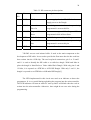
LIST OF TABLES
TABLE
TITLE
PAGE
2.1
The OSI function
11
3.1
RCT-433-AS pin descriptions
26
3.2
ISP connector pin descriptions
28
xi
LIST OF FIGURES
FIGURE
TITLE
PAGE
1.1
Flash flood incident in Johor Bharu
2
1.2
System development processes
4
2.1
Wireless sensor network applications
7
2.2
Non-Contact Water Level Measurement
12
2.3
High water indicator and low level water controller
13
3.1
Hardware development Flow chart
16
3.2
Wireless sensor network block diagram
17
3.3
Transmitter Node Block Diagram
18
3.4
Water Level Sensor Schematic Diagram
19
3.5
Atmega8535 pin configuration
22
3.6
Voltage regulator schematic diagrams
22
3.7
Microcontroller Board Schematic Diagram
24
3.8
RCT 433 AS transmitter module
25
3.9
ISP cable Schematic Diagram
27
3.10
Software development flow chart
30
3.11
Sensor reading flowchart
31
3.12
Transmitted data frame format
32
3.13
Data Transmission flow chart
33
3.14
WinAVR notepad and makefile window
35
3.15
PonyProg window
36
4.1
Processor board
39
4.2
Water level sensor
39
4.3
RF Transmitter modules
39
4.4
Water Sensor System Prototypes
40
4.5
ISP Cable
41
4.6
C Language program in WinAVR Programmer Notepad
42
xii
4.7
Measured input voltage for processor board
43
4.8
Sensor data transmission (hyperteminal)
43
4.9
Sensor data transmission (oscilloscope)
44
4.10
Communication terminals for wired data
45
4.11
Observed data during wired transmission
46
4.12
Observed data during wireless transmission
47
4.13
GUI water level indicators
48
xiii
LIST OF ABBREVIATIONS
ADC
Analog to Digital Conversion
AVRGCC
AVR-GNU Compiler Collection
AVR RISC
AVR Reduced Instruction Set Computer
COM1
Serial communication port 1
CPU
Central Processor Unit
EEPROM
Electrically Eraseable Programmable Read Only Memory
FTP
File Transfer Protocol
ISP
In-Circuit Serial Programmable
KB
Kilo Byte
LSB
Least Significant Bit
MHz
Megahertz
MSB
Most Significant Bit
OS
Operating System
PPP
Point to Point Protocol
RAM
Random Access Memory
RF
Radio Frequency
Rx
Receiver
SLIP
Serial Line Interface Protocol
TCP/IP
Transmission Control Protocol/ Internet Protocol
Tx
Transmitter
UDP
User Datagram Protocol
USART
Universal Synchronous Asynchronous Receiver Transmitter
xiv
LIST OF APPENDICES
APPENDIX
TITLE
PAGE
A
Transmitter node source code
54
Transmitter node makefile
59
RF Module Data Sheet
66
Atmel Atmega8535 block diagram
70
C
Graphical User Interface Result
71
D
Ponyprog Manual
73
B
CHAPTER 1
INTRODUCTION
1.1 Overview
Sensor network composes of large number of sensor nodes, which
communicate with each other. Sensor network deployments were envisioned to be
done in large scales, where each network consists of hundreds or even thousands of
sensor nodes. These sensor nodes work by gathering their sensing information and
sent the data trough the network using specific address. The main characteristic of
sensor node is said to be physically small and inexpensive. Basically a sensor node
consists of one or more sensor, a short-range radio transmitter or transceiver, a small
microcontroller and a power supply in form of battery.
This project implements a water level sensor as a sensor node. The sensor
node will communicate between the transmitter and receiver node using wireless
transmission. The embed sensor will measure 4 different water levels and sends the
data from the transmitter directly to the desired receiver. A wireless communication
will be used throughout the project. This system consists of a microcontroller, RF
transmitter, water level sensor and power supply.
2
1.2 Problem Statement
Water level sensor system was built appropriate with flood issue that hit our
country every year. This issue forms many problems and trouble to the resident
within the hit area. Most of them are left with nothing neither shelter nor property.
Other than that, the wireless sensor network was chosen based on its performance.
This system can be placed directly to the phenomena. Thus the precise data will be
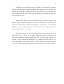
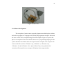
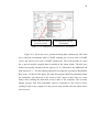
achieved. Figure 1.1 shows the latest flash flood incident that hit Johor Bharu
reported in Berita Harian on November 1st, 2006. The aerial view of the phenomena
showed the vehicles trapped in the flood at Johor Bharu.
Figure 1.1 Flash flood incident in Johor Bharu
Moreover the wireless sensor network operates in real time operation.
Therefore this system is very convenient since data is transmitted and received at a
specific time. Other than that, the rapid growth of wireless sensor network
technology is also one of the reasons why this project was developed.
3
1.3 Objectives
The objective of the project is to create a sensor node that is able to do
sensing processing and communicating between nodes. The sensor involved in this
project is water level sensor. Most wireless sensor network developments are
implemented close to the actual phenomena. The water level system is linked to a
water level sensor so it can measure 4 levels of water before it reaches the maximum
level. In order to apply this sensor, it must be placed near the riverbank. This sensor
needs to be controlled by a microcontroller and the data might be sent via the
wireless network. By completing this sensor node, perhaps it can perform
accordingly to the design and present its task successfully.
1.4 Scope of work
In general, this project was divided into 2 parts; the transmitter and the
receiver. Each part was developed separately and combined at the end of this project.
The development of transmitter node consists of 3 main stages which are the
hardware development, software development and finally a complete system
development.
First and foremost, this project focuses on the development of a sensor node
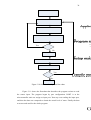
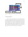
that can communicate wirelessly in wireless sensor network. Figure 1.2 shows the
block diagram of the system development. First, it is necessary to get the overview
and learn deeply this system functions. Next is the hardware development in wireless
sensor network. Commonly, a sensor node consists of a microprocessor, a sensor, a
radio frequency transmitter and power supply. Complete systems block diagram need
to be designed and the step of work need to be planed so that the system will be
implemented according to the schedule. After that, the sensor node requires the
software development. The microprocessor needs to be programmed to ensure its
function. It must be programmed according to the application.
4
Schedule / plan
of work
Whole system
overview
Hardware
development
Software
development
Figure 1.2 system development processes
1.5 Thesis outline
This thesis consists of five chapters. Chapter 1 briefly explains the
development of water sensor system. It describes the reason of developing this
system, the objective of developing water sensor system and as well as the scope of
work involved while the system was developed.
Chapter 2 clarifies on the idea about the development of water sensor system.
It includes the overview of wireless sensor network, the fundamental knowledge in
TCP/IP protocol, design architecture and the alternative sensor to be chosen for the
water sensor development. Then, Chapter 3 elaborates the process of completing the
project. It explains the step by step work to complete the water sensor system which
includes the development of hardware and software.
Chapter 4 discusses results and analysis of water sensor system. In this
chapter, the results taken from the sensor node is analyzed. Data is captured using
oscilloscope during data transmission. Finally, chapter 5 concludes the overall
performance of the system and suggests the possible enhancement that can be done
to improve the wireless sensor network performance.
CHAPTER 2
Literature Review
2.1 Wireless Sensor Network Overview
Wireless sensor network describes accumulate numbers of nodes within an
area. It consists of distributed sensors to monitor physical or environmental
conditions, such as water level, temperature, sound, vibration, pressure, motion or
pollution taken at different locations. Wireless sensor network development is
originally inspired by military application such as battlefield surveillance. The sensor
nodes represent significant improvement compare to ad hoc sensor. The major
difference is in sensor networks the sensor can be placed directly to the phenomena.
Sensor network also allows the deployment in inaccessible terrain.
2.1.1 Basic concept of wireless sensor network
Most sensor node application aims at monitoring or detection of a
phenomenon. Sensor nodes are densely deployed either inside the phenomena or
very close to it. It can be an advantage to get the actual precise data compared to the
conventional sensor. Examples of sensor node application includes weather
forecasting, humidity detector, wind speed detector, earthquake detector by reading
the vibration of earth surface, water level sensor for flood prevention, forest fire
detection and wild life habitat monitoring.
6
Another unique feature for sensor node is its mobility and it can be remotely
monitored. To achieve this remote access monitoring, sensor node can be connected
to an existing network infrastructure such as the global internet, local area network or
private intranet. Since the sensor node is equipped by on board processor, instead of
sending the raw data to the node responsible for the fusion, sensor node uses its
processing ability to locally carry out simple computation and transmit only the
required and partially processed data.
2.1.2 Application of wireless sensor network
The range of wireless sensor network usage can vary from ecological to
social applications in everyday world. Figure 2.1 shows some examples of sensor
network applications which can generally be categorize as military applications,
environmental applications, Health applications, home applications and other
commercial applications. In the military application, the implementation of wireless
sensor network is the best idea since sensor networks are based on the dense
deployment of disposable and low-cost sensor nodes. Destruction of some nodes by
hostile actions does not affect a military operation as much as the destruction of a
traditional sensor, which makes sensor networks concept a better approach for
battlefields [11].
Similar with the implementation of wireless sensor network in the battle field,
implementing the wireless sensor network for environmental application might be
very helpful. Some examples of environmental applications of sensor networks
include tracking the movements of birds, small animals, and insects; monitoring
environmental conditions that effects may harm the surroundings such as forest fire
detection, flood detection and precision agriculture.
7
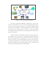
Wireless Sensor
network
application
Figure 2.1 Wireless sensor network applications
Other than environmental applications, employing the wireless sensor
network for health application can be very useful. Some health application based on
wireless sensor network provide interfaces for the disabled, integrated patient
monitoring, wireless diagnostics, remote drug administration in hospitals, monitoring
the movements and internal processes of insects or other small animals,
telemonitoring of human physiological data, and tracking and monitoring doctors and
patients inside a hospital.
With the rapid growth in technology, applying wireless sensor network for
home appliance is one of the best ideas. A smart home technology demands a tiny
node to be implemented directly to home appliance and help the owner manage their
home devices remotely. The other implementations for wireless sensor network are
the commercial applications such as monitoring material fatigue, building virtual
keyboards, managing inventory; monitoring product’s quality, constructing smart
office spaces and environmental control in office buildings.
8
2.1.3 Factors influencing sensor network design
The factors that drive the design of sensor networks and sensor nodes also
cannot be neglected. These factors are important because they serve as a guideline to
design a protocol for sensor networks. In addition, these influencing factors can be
used to compare different schemes [11]. Sensor network design can be influence by
numerous factors includes fault tolerance. Fault tolerance is the ability of wireless
sensor network to sustain network functionality without any interruption due to
sensor node failure [11]. Low fault tolerance is required for low interference
environment and vice versa. The other factor is production costs. Cost of each sensor
nodes has to be kept low. The cost should not be above than Bluetooth and satellite
technology.
Besides cost, a hardware constraint is also the main factor that influences
sensor network design. Sensor node is made up of four basic components including
sensor, microprocessor, radio frequency module and power unit. The implementation
processor board is depends on the application or sensor used by the sensor node.
Environment also can be the main factors that influence the sensor node design. The
sensor nodes can directly deploy to the actual phenomena. It also may work in
remote geographic areas. The sensor node can also work under high pressure in the
bottom water, in harsh environment and also under extreme heat and cold. So, the
correct component must be selected to ensure the performance of the sensor node.
The next factor is the transmission media. Wireless sensor network is linked
by a form of radio frequency module, infrared or optical media. Various transmission
medium enable global operation of these networks worldwide. For example the radio
frequency module and a variety of modulation technique can be used to be
implemented in the wireless sensor network. The selection of the modulation
technique also is depends on other factors discussed previously. Various frequency
bands are available for sensor nodes applications. The last factor that influences the
design of wireless sensor network is power consumption. The wireless sensor node
can only be equipped with a limited power source. One of the examples is the 3-9 V
9
battery sources. In some application scenarios, replacement of power resources might
be impossible. The sensor node lifetime strongly depend on battery source.
2.2 Radio frequency modules
Radio Frequency modules are partially complete circuits that can be
incorporated into larger designs. RF modules include receivers, transmitters and
transceivers. RF modules employ numerous dissimilar modulation technique and
radio system. An examples of modulation technique used in RF module is Phaseshift keying (PSK) which is a digital modulation scheme that conveys data by
changing, or modulating, the phase of a reference signal (the carrier wave). Other
examples are amplitude modulation (AM), Frequency modulation (FM), Amplitude
shift key (ASK), Frequency shift key (FSK) and Phase shift key (PSK).
The numerous modulation techniques have their description. On off key, it
can be described as a binary form of amplitude modulation. Other than that
amplitude modulation explains as a technique used in electronic communication,
usually for transmitting information using a carrier wave wirelessly. Amplitude
modulation works by varying the strength of the transmitted signal in relation to the
information being sent [9].
Next is the frequency modulation technique. FM is a form of modulation
which represents information as variations in the instantaneous frequency of a carrier
wave. In analog applications, the carrier frequency is varied in direct proportion to
changes in the amplitude of an input signal. Digital data can be represented by
shifting the carrier frequency among a set of discrete values, a technique known as
frequency-shift keying [7].
Besides FM, the other modulation technique is frequency shift keying.
Frequency shift keying is a digital modulation scheme that conveys data by
changing, or modulating, the frequency of a reference signal (the carrier wave).
10
Meanwhile the Amplitude-shift keying (ASK) is a form of modulation which
represents digital data as variations in the amplitude of a carrier wave. And finally
Phase-shift keying (PSK) is a digital modulation scheme that conveys data by
changing or modulating the phase of a reference signal.
2.3 Sensor network communication architecture
Sensor network may operate in different geographic areas and in any
unsecured environment; therefore security should be built into the design. Network
techniques are needed to provide low-latency, survivable, and secure networks. Low
probability of detection communication is needed for networks because sensors are
being envisioned for use behind enemy lines. For the same reason, the network
should be protected against intrusion and spoofing [12].
The approach to design protocols for sensor networks is driven by the
requirements of the physical layer. The protocols should be developed according to
the choice of physical layer components, such as the type of micro-processors and
the type of RF modules [11]. The approach of the wireless sensor node also
highlights the importance of the application layer, network layer, MAC layer, and
physical layer to be integrated with sensor nodes hardware. Sensor network protocol
has to be aware of the hardware and able to use special features of the
microcontroller and transmitter to minimize the sensor node’s power consumption.
Those approaches to design the protocol describe how data communications
should take place. In OSI model, each layer performs the function required to
communicate with another system. Every layer provides service for its higher layer.
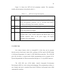
Table 2.1 validates the function of every layer in OSI Model.
11
Table 2.1
The OSI function
Layers
Function
Application
Provides access to the OSI environment for user and also provide
distributed information services
Presentation Provides independence to the application process from difference in
data representation (syntax)
Session
Provides
the
control
structure
for
communication
between
applications; establish, manage, terminate the connection between
cooperating systems
Transport
Provides reliable transparent transfer of data between end points;
provides end to end error recovery and flow control
Network
Provides upper layers with independence from the data transmission
and switching technologies used to connect system; responsible for
establishing, maintaining, and terminating connections.
Data Link
Provides the reliable transfer of information across the physical link;
sends blocks ( frame) with necessary synchronization, error control
and flow control
Physical
Concerns with transmission of unstructured bit stream over physical
medium; deals with mechanical, electrical, functional, and procedural
characteristics to access the physical medium
This system deploys the first 2 bottom layer of OSI model which consist of
Data link and Physical layer. Non- standard protocol is implemented for the system
for communication. Physical layer provides the electrical and mechanical interface to
the network medium which is represented by the wireless link. By providing the
interface, it offers data-link layer the ability to transport a stream of serial data bits
between two nodes in the system. The physical layer is also responsible for making
sure that the bits are safely sent from one place to another, by considering other
factors such as modulation technique, and deals with the electrical characteristics of
the wireless link.
12
2.4 Water Level Sensor
For the environment application, variety choices of water level sensors have
been manufactured and produced. These water level sensors mostly employ a high
technology system to measure a very accurate level, for examples ultrasonic water
level sensor produced by Global Water Instrument, INC. The system uses the latest
ultrasonic distance measuring technology for accurate non-contact water level
monitoring.
The fully encapsulated sensor/transmitter is temperature compensated and
provides an industry standard 4-20 MA output. There are three ranges available
including 1’, 3’, 6’, and 35' to meet a wide variety of applications. The unique 1’
range ultrasonic water level sensor is ideal for measuring flow in small flumes and
weirs. The 3’ and 6’ ultrasonic water level sensor ranges are best for measuring
river, lake and tank levels and for measuring open channel flow in larger flumes [10].
Figure 2.2 shows the non contact water level measurement by Global Water
Instrument.
Figure 2.2 Non-Contact Water Level Measurement
13
Besides ultrasonic technology, water level alarm sensor by Global Water is
also a unique choice. It is a solid state water sensor for detecting the presence of
conductive solutions, such as water spills, water tank levels, and drainage ponds. The
water alarm sensor features two stainless steel electrodes that are positioned at a
desired point for liquid detection. When fluid is detected, a relay closes in the water
level alarm and the signal can be used to sound an audible alarm or close a switch
inside a piece of remote monitoring equipment. The relay output is fully isolated and
can handle 2 amps of current.
If the water level alarm sensor sense in a dry conditions, the detection sensor
will automatically reset without requiring additional service. The water level alarm
is rugged and durable and requires minimal maintenance. The water level alarm has
many uses, including surface water monitoring, precision level detection, water level
control, high water indication, and submersible marine low level indication [10].
Figure 2.3 shows the high water indicator and low level water controller that can be
implemented as the alternative sensor for this system.
Figure 2.3 High water indicator and low level water controller
CHAPTER 3
METHODOLOGY
3.1 Introduction
This chapter describes the method used in order to complete water sensor
system. It consists of the design process of water sensor system. The development of
water level sensor has been made possible by a number of technological
developments including the miniaturization of electronics and sensors. Generally the
design processes are divided into three phases. They are the initial electronic design
or the hardware development, sensor node programming or the software
development and the final phase, the overall system testing development. In order to
achieve the objectives of this project, it is important to figure out what is the finest
technique and proper step in designing the sensor node. The microcontroller circuit
should suit best the sensor implementation to achieve the greatest performance
during transmission.
3.2 Hardware Development
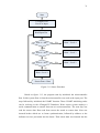
Figure 3.1 gives an idea about the steps followed in order to finish this
project. The initial state is about getting the brief idea about what is wireless sensor
network, what components each node in the network consist and finally distribute
these nodes into transmitter and receiver part. The project is then divided into 2 parts
which is the transmitter and the receiver part. In the transmitter part, it is essential to
15
choose the appropriate sensor to be developed in the project. The sensor application
must be suitable with the microprocessor so that the program written for the sensor
can be fit into the microprocessor memory. Other than that, the output voltage from
the sensor also must be within the microprocessor range which is 4.5-5.5 volt. It is
important to keep the voltage level within the range because at this range the
microprocessor will work efficiently. If the sensor voltage level is out of range,
microprocessor may not detect the signal sent by the sensor.
In figure 3.1, the next step after selecting the appropriate sensor is sketching
the system block diagram. System block diagram illustrates each part on the system
development. It gives the brief idea on the water sensor system development. Next is
the water sensor and microcontroller circuit design using multisim software. Then
the circuit is simulated using the same software to ensure that the circuit is free from
error.
After completing with the circuit design, the project continus by assembling
the circuit on the test board. Then the circuit is tested using multimeter and
oscilloscope. Sensor circuit is tested to obtain the suitable voltage level according to
the microprocessor’s operating voltage range. Other than that, the microprocessor
board must be tested to ensure that it receive the stable input voltage. Stable input
voltage refers to the steady voltage value supplied to VCC pin. It is essential to
obtain this level to make sure the microprocessor performs efficiently and to avoid
any error from occurring during data transmission.
Hardware designing is the critical phase in this project. Any failure on the
hardware part will affect the overall system. A troubleshoot and redo work must be
done if any error is detected during the hardware development process. The final step
after hardware development is software development. This phase involve a few
software which will be discussed in detail in the next topic in this chapter.
16
Start
Overview about Wireless Sensor Network
(WSN)
Divide WSN into 2 nodes.
Transmitter and Receiver.
(Assigned to transmitter end)
Select appropriate sensor to be implemented in WSN
Design system block diagram
Design sensor and microcontroller circuit
Simulate circuit using multisim
yes
Redesign and
retest circuit
Error?
no
Purchase component and assemble circuit on test board
Run test on circuit using multimeter and oscilloscope
yes
Troubleshoot and
repair
Error?
no
Software development
Figure 3.1 Hardware development Flow chart
17
Water
Level
Sensor
Microcontroll
er
ATMEL
ATmega8535
Microcontroll
er
ATMEL
ATmega8535
Transmitter Node
Receiver Node
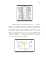
Figure 3.2 Wireless sensor network block diagram
The network block diagram is showed in figure 3.2. As shown in figure 3.2, a
set of wireless sensor network consist of 1 unit of microcontroller at each part, radio
transmitter and receiver, one or more sensor depending on the application and as well
as energy source. Microcontroller is the main component for each node in sensor
network. Microcontroller is used to process data sense from the sensor; send the data
through the network and to extract data that have been received.
As mention before, in the transmitter part, it is essential to select the suitable
sensor to be implemented in and communicate in the network. Water level sensor
was selected due to the current issue regarding flood and the profit loss by the flood
victim.
Transmitter node block diagram which include a sensor, radio frequency
transmitter and a Microcontroller is shown in figure 3.3. Water level sensor was
linked to Port A, Radio frequency module connected to Port D and ISP cable as the
code downloader was connected to Port B.
18
ISP
Connector
Port B
TX Module
433 MHz
Port D
Port A
Water Level
Sensor
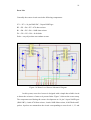
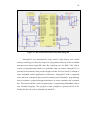
Figure 3.3 Transmitter Node Block Diagram
Transmitter node design consists of water level sensor schematic circuit and
microcontroller schematic circuit. Both sensor and microcontroller schematic circuits
are showed in figure 3.4 and figure 3.7. Data from sensor is linked to the
microcontroller board by a direct wire. The microcontroller then processes the data
captured by water level sensor and as a final step the data is sent over the network
using radio frequency transmitter that operates in 433MHz.
3.2.1 Sensor
Sensor can be described as any device that receives a signal or stimulus and
react to it in a distinctive manner or in other words sensor is an electronic device
used to measure a physical quantity such as temperature, pressure or loudness and
convert it into an electronic signal of some kind (e.g a voltage). Sensors are normally
components of some larger electronic system such as a computer control or
measurement system. Analog sensors most often produce a voltage proportional to
the measured quantity. The signal must be converted to digital form with an ADC
before the CPU can process it. Digital sensors most often use serial communication
such as RS-232 to return information directly to the controller or computer through a
serial port.
19
Parts List
Generally the sensor circuit consist the following components:
IC1 = IC2 = 14 pin D4011BC, 2 input NAND get
R2 = R3 = R6 = R7 = 470 ohm resistor
R1 = R4 = R5 = R8 = 180K ohm resistor
D1 = D2 = D3 = D4 = 4148 diode
Probe = any object that can conduct current.
Figure 3.4 Water Level Sensor Schematic Diagram
In this system, water level sensor is designed with a simple but reliable circuit
to detect the existence of water at 4 present limits. Figure 3.4 shows the sensor setup.
The component used during the sensor development are 14 pin 2 input NAND gate
(D4011BC), 4 units 470 Ohm resistor, 4 units 180K Ohm resistor, 4148 Diode and 5
probes. 4 probes are mounted on the circuit corresponding to water levels 1, 2 3 and
20
4. Any object that is able to conduct current can be used as a probe. The probe will
work together with VCC probe. The VCC probe must be deployed deeply into the
water. LED is used as the indicator that represents the water level. LED 1 represents
level 1 and so on. Diode that is attached at the output of the IC used to block any
feedback current. It can prevent any overload current from damaging the IC. This
sensor will operate at 9 V operating voltage.
Water level sensor starts functioning when the water level reached probe 1
which is the first level and it will short circuit IC1 pin 1. The output from this IC
which is pin 4 will turn on the first LED. If water didn’t reach the first probe, the
sensor will remain idle and microprocessor will read the sensor data as “0” or very
stable condition.
The measuring process will continue and function appropriately according to
the increment of the water. The LED will remain on as the water level increase to the
next level which is level 2, 3 and 4. The critical situation will occur when all LEDs
are turned on. It indicates that the water has reached the maximum level. Output
from this sensor is connected directly to the microprocessor. Voltage measured at pin
4 and 10 of each IC are around 4.8 V and can effectively work with the
microprocessor.
It is essential to take every precaution to avoid short circuit since water is also
an electric conductor. This sensor must be placed far from the water source to avoid
any short circuits.
21
3.2.2 Processor
The processing unit, which is commonly connected with a small storage unit,
handles the procedures that make the sensor node work together with the other nodes
to carry out the assigned sensing tasks. Processor can be defined as a single-ship
device that contains memory for programmed information and data. It has logic
programmed control reading inputs, manipulating data, and sending outputs. In other
words, it has a built-in interface for input/output (I/O) as well as a central processing
unit (CPU) [8]. The microcontroller unit is generally referred as MCU.
An 8 bit AVR RISC microcontroller is selected as the brain of water sensor
system. The processor is selected based on its memory utilization. This processor has
provides interesting features such as 8K bytes of in-system programmable flash with
read while write capabilities, 512 bytes EEPROM, 512 bytes SRAM, 32 general
purpose working registers, three flexible timer/counter with compare modes, internal
and external interrupt, a serial programmable USART, a byte oriented two wire serial
interface, an 8 channel 10 bit ADC, a programmable watchdog timer with internal
oscillator, an SPI serial port and six software selectable power saving modes [5].
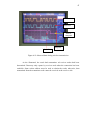
Figure 3.5 illustrate the Atmel Atmega8535 pin configuration. It shows all
connection of I/O port, oscillator connection pin, USART transmit and receive pin
and ADC port. This configuration must correctly follow the Atmel AVR datasheet to
ensure the processor operate properly. This system utilizes almost the entire
Atmega8535 pin out.
22
Figure 3.5 Atmega8535 pin configuration
As illustrated in figure 3.5, to enable the Microcontroller, it is essential to
provide it with the suitable voltage. Referred to the datasheet, operating voltage for
Atmega8535 is between ranges 4.5 V until 5.5 V. At this level, this microcontroller
unit will function effectively. To obtain the optimum value of power source, a 5 Volt
voltage regulator circuit was applied on the Microcontroller board. This circuit
ensures that the Microcontroller received less than 5.5 Volt of supply during its
operation. If more than 5.5 Volt of voltage is supplied directly to the board, the
regulator decreased the value to avoid any damage to the microcontroller unit. Figure
3.6 shows the voltage regulator schematic diagram.
Figure 3.6 Voltage regulator schematic diagrams
23
ATmega8535 microcontroller uses an 8 MHz crystal oscillator to generate
external clocking. Radio frequency transmitter was connected to pin 15 which are the
USART pin, PORT B is applied for an ISP cable which is use to program the
microcontroller directly on the circuit board, and PORT A was assigned as input port
to read data from sensor.
Output gained from sensor was connected to PINA 1, PINA 2, PINA 3 and
PINA 4. Each pin indicated different level of water which PINA1 is represent lowest
water level while PINA 4 represent the highest or critical level. To ensure that
PORTA can read the data captures by the sensor, the sensor itself must generate
output voltage at 4.5 V – 5.5 V range.
Besides the register, the other pin that needed the special attention is pin 30
which is the AVCC. AVCC is the supply voltage pin for Port A and the A/D
Converter. It should be externally connected to VCC, even if the ADC is not used. If
the ADC is used, it should be connected to VCC through a low-pass filter [5]. To
ensure the stability of the voltage supply, a 100 nF capacitor was connected to the
VCC input. These capacitors should be placed as close to the power pins as possible.
24
Figure 3.7 Microcontroller Board Schematic Diagram
Atmega8535 was manufactured using Atmel’s high density non volatile
memory technology. It allows the chip to be reprogrammed directly on the assembled
microprocessor board using ISP cable. By combining an 8 bit RISC CPU with in
system self programmable flash on a monolithic chip, the Atmel Atmega8535 is a
powerful microcontroller that provides highly flexible and cost effective solution to
many embedded control applications. Furthermore, Atmega8535 AVR is supported
with a full suite of program and system development tools including C programming,
macro assemblers, program debugger/simulators, in circuit emulators and evaluation
kits. This microcontroller can be program using C programming, MikroBasic and its
own assembly language. This program is then compiled to generate the Hex file.
Finally this Hex file will be uploaded into the MCU.
25
3.2.3 RF Module
Radio Frequency modules are partially complete circuits that can be
incorporated into larger designs. RF modules include receivers, transmitters and
transceivers. RF modules employ numerous dissimilar modulation technique and
radio system. The examples of modulation techniques use in RF module are on-off
key (OOK), Amplitude modulation (AM), Frequency modulation (FM), Amplitude
shift key (ASK), Frequency shift key (FSK) and Phase shift key (PSK).
Performance criteria for RF modules consist of sensitivity, output power,
communication interface, operating frequency, and maximum transmission distance.
Sensitivity described as a minimum input signal necessary to construct a specified
output signal. Output power is the maximum signal power that RF modules can
transmit. Operating frequency is the range of transmitted and received signals. Last
but not least, maximum transmission distance is the maximum range that a
transmitter and receiver can be separated.
A low cost stabilized surface mount RF transmitter RCT-433-AS from
Radiotronix was chosen to be implemented in this system. This RF module includes
a 433.92 MHz amplitude modulation version, 1.5-12V voltage operation, 5mA
current consumption, small size, 0dBm output power and 4800 baud operation. The
RCT-433-AS module is ideal for remote application where low cost and longer range
are required. The 1.5 to 12 Volt operation voltages make it ideal for battery power
applications. The transmitter utilizes a Surface Acoustic Wave (SAW) stabilized
oscillator to ensure precise frequency control for best range performance.
Figure 3.8 RF module
26
Figure 3.8 shows the RCT-433-AS transmitter module. The transmitter
module pin description is described in table 3.1:
Table 3.1
Pin
Pin
No.
Name
1
ANT
RCT-433-AS pin descriptions
Description
50 ohm antenna output. The antenna port impedance affects output
power and harmonic emissions. An L-C low-pass filter may be
needed to sufficiently filter harmonic emissions.
2
GND
Transmitter ground. Connect to ground plane.
3
DATA
Digital data input. This input is CMOS compatible and should be
driven with CMOS level inputs.
4
VCC
Pin 4 provides operating voltage for the transmitter. VCC should be
bypassed with a .01uF ceramic capacitor and filtered with a 4.7uF
tantalum capacitor. Noise on the power supply will degrade
transmitter noise performance.
3.2.4 ISP Cable
One unique features offer by Atmega8535 is this chip can be program
directly on the circuit board. Atmel offer a package call The Atmel AVR ISP which
is In-System Programmer for Atmel’s AVR Flash Microcontrollers. The AVR ISP
gives the developer a compact and reliable programming tool to program all InSystem Programmable AVR microcontrollers through a 6- or 10-pin ISP connector.
The AVR ISP uses AVR Studio, Atmel’s Integrated Development
Environment (IDE) for code writing and debugging. The programming software is
user friendly and can be controlled from both a Windows environment and a DOS
command-line interface.
27
Instead of using AVR ISP offer by the Atmel, developer also can build its
own ISP cable. This ISP cable has the similar function with AVR ISP offered by
Atmel. The ISP cable schematic diagram was illustrated in figure 3.9. This cable was
cheap and effortless to build up. It can be the ideal starting for the developer.
Figure 3.9 ISP cable Schematic Diagram
Components required in order to develop ISP cable are a DB25 connector,
74LS245 chip, 6 pin header, a 470 ohm resistor, a LED as a power indicator and
jumper cables. There are 6 signals to be implemented in developing an ISP cable. It
consist Master Out Slave in (MOSI) pin, Master in Slave out (MISO) pin, Shift
Clock (SCK) pin and RESET pin. Another 2 pin are for VCC and ground. The
function of ISP Connector pin is explained in table 3.2. The pin sequence followed
the ISP conn pin header in the schematic.
28
Table 3.2 ISP connector pin descriptions
Pin
Name
Function
Description
VCC
ISP Power
Power supply for the ISP. ISP header must
No
1
supply power to the Dongle
2
3
MOSI
Master Out
Data being transmitted to the part being
Slave In
programmed is sent on this Pin
RESET Target MCU
Connect to target AVR. Target AVR is
Reset
programmed while in Reset State
4
SCK
Shift Clock
Serial Clock generated by the Programmer
5
MISO
Master In Slave
Data
Out
programmed is sent on this pin
Ground
Common Ground
6
GND
received
from
the
part
being
74LS245 was an octal tristate buffer. It used as the main component to the
development of ISP cable. It was used to provide the float state after the hex code has
been written into the AVR chip. The two loop-back connections, pin 2 to 12 and 3
and 11 is used to identify the ISP cable or so called as dongle. With both links in
place the dongle is identified as a Value Added Pack Dongle. With only pins 2 and
12 links, it is reported as a STK300 or AVR ISP Dongle. With only 3 and 11, the
dongle is reported as an STK200 or old Kanda ISP Dongle[1].
The LED implemented in this circuit was used as an indicator to detect the
programmer. It is very useful during uploading the program into the microcontroller.
The LED indicator will turn on when PC start up and it will blink when the code in
written into the microcontroller. Otherwise, there might be an error arise during the
programming.
29
3.3 Software development
Software development was the crucial part while developing this system. A
lot of rework needs to be done when the result didn’t achieve the initial target. In
general, there are three major tasks need to be performed by sensor node which is
read data from sensor, process the data to include data header, address, sensor data
and frame check sequence and finally send the data to the receiver. As illustrated in
figure 3.10, the work flow began by building the application flowchart. This
flowchart was a necessary guideline to be follow during accomplishing the system.
Next step is writing a program according to the application. The program was written
in C programming. After that, a make file was set up. Make file was essential
because it can determines the types of linker, loader and the object files to be
produced.
After completing the program, it needs to be compiled. The written program
was compiled using WinAVR. WinAVR ensure that the codes generated from the
program are compatible with Atmega8535. This point demands a lot of rework if any
errors are detected during compiling. The system need to be altered and reprogram to
resolve the error. Once the programs are free from error, WinAVR compiler will
generate a Hex file. This is a very useful file that required to be uploaded into the
microcontroller unit.
After the Hex file were uploaded into the microcontroller unit, the whole
circuit can be tested either it compatible or function accordingly to the application.
Rework also necessitate if the expected result couldn’t be obtained.
30
Yes
No
Yes
No
Figure 3.10 Software development flow chart
Figure 3.11 shows the flowchart that describes the program written to read
the sensor input. The program began by port configuration. PORT A at the
microcontroller unit was assign as input port. Nest step was reading the input port,
and then the data was compared to obtain the actual level of water. Finally the data
was store and used for the whole program.
31
Start
Configure Port
Port A as Input
Read Input Pin
Port A = $0F?
Yes
Data = Level 4
Yes
Data = Level 3
Yes
Data = Level 2
No
Port A = $07?
No
Port A = $03?
No
Data = Level 1
Sensor Data = Data
Figure 3.11 Sensor flowchart
Based on figure 3.13, the program start by initialized the microcontroller
Port. In this system Port A from the microcontroller was used as the input port. The
steps followed by initialized the USART function. Those USART initializing codes
can be referring in the ATmega8535 Datasheet. Water sensor system employs a
serial communication to transfer between two microcontrollers. The next step was
read the sensor data. Data read from sensor the stored as sensor data. Next was
inserted header which use as frame synchronization, followed by address as the
indicator receiver port name into the frame. Then sensor data was inserted into the
32
frame, followed by checksum. Checksum is an error- detecting code based on a
summation operation performed on the bits to be check. The formula to generate
Checksum Code is:
Checksum = - (Header1 + Header2 +Address1 + Address2 + Data)
The sensor data then send through the network in a form of frame as shown in
figure 3.12
Header
Address
Sensor Data
Checksum
(2 Bytes)
(2 Bytes)
(1 Bytes)
(1 Bytes)
3.12 Sensor data frame format
33
Start
Initialize port
Initialize USART
Read Sensor Data
Sensor Data = Data
Insert header
Insert Address
Insert Sensor Data
Calculate Checksum
Checksum = - (Header 1 + Header 2 + Address 1 + Address 2 + Data)
Insert Checksum
Transmit data
Figure 3.13 Data Transmission flow chart
34
3.3.1 Code development
Several software was involved to accomplish this project. The source code
was written in C language. The code written need to be complied to generated the
Hex file and finally the Hex file was uploaded into the microcontroller unit. The
choice of software used are depends on the most convenient way to implement the
code generated into the microcontroller unit. Two major software that mostly used
during completing this system are WinAVR and PonyProg.
3.3.1.1 WinAVR
The initial step was writing the source code in C programming language. For
this purpose, the code can be written in Visual C, notepad or WinAVR programmer
notepad. On the other hand, for compiling purpose, a WinAVR code compiler was
used to compile the written program and generated the Hex file. This software was
choose since it offer a complete development tools including the programmer
notepad, compiler, Assembler, linker, AVR library , file converter, debugger and so
on. WinAVR compiler was complete software while developing this project. It is
flexible and can be hosted on many platforms. Furthermore, WinAVR can target
many different processor and extremely compatible for most Atmel’s ICs.
There are a few steps to be followed while writing a program using this
software. First step was writing the source codes and save it in a specified folder.
Then save the file created according to the source codes language. For example .asm,
.c, etc. In this case the file must be saved as filename.c.
After that, the next step was edited the makefile according to the target
device. Makefile is a text file that that lists and controls the program and the
microcontroller unit. Three changes need to be done. First, change the PRG and OBJ
to the name of the source code and lastly edit MCU_TARGET depends on what type
of microcontroller used. If these steps were missing, an error may occur because the
35
program didn’t recognize the registers use in the program. Afterwards, the makefile
was saved in the same folder for source code file.
In order to clean any existing file except for the code and makefile, make
clean command was choose in the tools panel. Finally, choose make all command in
the tools panel to make all file for the program such as filename.lst, filename.obj and
filename.hex. Those three file is the code used and will be uploaded into the
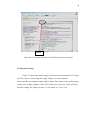
microcontroller. Figure 3.14 show the programmer notepad of WinAVR window
environment. The main program is shown at the back window and the upper
windows illustrate the makefile setup for the system main program.
Main program
Make file
Figure 3.14 WinAVR notepad and makefile window
36
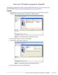
3.3.1.2 PonyProg
The next step after generating the Hex file is uploading the generated Hex file
into the microcontroller. To uploading the Hex file, the other software was used
which called PonyProg. PonyProg is serial device programmer software with a user
friendly GUI framework available for Windows95, 98, 2000 & NT and Intel Linux.
Its purpose is reading and writing every serial device. PonyProg works with other
simple hardware interfaces like AVR ISP (STK200/300), JDM/Ludipipo, EasyI2C
and DT-006 AVR (by Dontronics) [3]. The PonyProg window shown in figure 3.15.
Hex Code
Source Code
ASCII’s
representation
Microcontroller
memory
Free Buffer
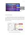
Figure 3.15 PonyProg window
37
The figure 3.15 shows the hex file generated after compiling the source code
in WinAVR. The Ponyprog window contains the Hex code compiled from the
original program written in C language, the source code ASCII’s representation,
microcontroller memory and the unused microcontroller buffer. The essential steps
require before using this software was first, setup the interface whether to use serial
or parallel connector. Secondly, calibrate the bus timing, define the device going to
be used and setup the configuration and security bits. One completing the calibration
and setting, the selected hex file can be downloaded into the microcontroller unit. It
is essential to ensure that right memory location has been chosen for the
programming either in flash or EEPROM memory. The full Ponyprog setup enclosed
in appendix D
CHAPTER 4
RESULTS AND ANALYSIS
Overall, this chapter discussed the result attained from the system
development and analysis for each result. The result was obtained from both wired
and wireless communication. Result obtained from these system output measured
using oscilloscope and the data transmitted can be read using USART terminal.
Some of the result was captured using ISIS Proteus software. Wave captured from
this software was similar with the data captured by the oscilloscope. To obtain the
result, this software read the data from RS232 connector that connected from the
microcontroller board to the computer. The results have been analyzed to guarantee
data collected at the receiver node is similar as transmitted at the transmitting node.
4.1 Hardware Development
As mentioned in chapter 3, water sensor system design process divided onto
three phases which are the electronic design or the hardware development, sensor
node programming or the software development and final phase, the overall system
testing development. This system successfully completed the first phase of the
system development which is the development of electronics components.
39
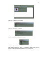
Figure 4.1 shows the completed processor board connected with the
transmitter module. Figure 4.2 shows the sensor built up to measure the water level.
Next figure 4.3 shows the RF transmitter module used to convey data wirelessly
from the transmitter node to the receiver node.
Processor board
Sensor Board
RF Transmitter modules
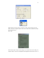
Figure 4.4 shows a complete system developed for water sensor system on
the transmitter node. The prototype includes the processor board, sensor board
transmitter module and a water level modeler. The sensor and processor board was
powered by 9 Volt Lithium batteries. At the processor board, 9 volt lithium batteries
connected to the voltage regulator to keep the supply lower than 5 Volt according to
the microcontroller operating voltage. The RF module use the same supply on the
processor board since its operating voltage may vary from 1.5 V to 12 V.
40
Figure 4.5 show the ISP cable which is In-System Programmer for Atmel’s
AVR Flash Microcontrollers. ISP simplified the code uploading process. By using
this cable, developer may program the generated code directly on the circuit board.
Unlike the ordinary boot loader, by using ISP cable, developer doesn’t have to plug
out the microcontroller unit in order to load the hex file.
Water level
modeler
Sensor
board
Processor
board
Transmitter
module
Figure 4.4 Water Sensor System Prototypes
41
Figure 4.5 ISP Cable
4.2 Software Development
The next phase of water sensor system development was built up the software
and writes a program in C language in the WinAVR programmer notepad. Afterward
the source codes will be compiled using WinAVR compiler. Figure 4.6 proved this
phase was completed. The back windows shows the C programming language for the
system and the front window shows the output from the compiler. The compiler will
create certain files such as <filename>.eep, <filename>.o, <filename>.obj,
<filename> .lst and <filename> .hex. Apart of that, if any error generated, the
execution will stop and it error message will display in the output window.
42
Output
Figure 4.6 C Language program in WinAVR Programmer Notepad
4.3 Measured Voltage
Figure 4.7 shows the voltage supply connected to microcontroller VCC input
pin. The purpose of measuring the supply voltage is to ensure that the
microcontroller was supplied with a stable voltage. This voltage is the similar output
voltage from voltage regulator circuit. The oscilloscope was set to 2V/div therefore
from the reading, the signal vary into 2 ½ box which is 2.5x2=5 volt.
43
2 ½ division x 2 volt = 5 volt
Ground level
Figure 4.7 Measured input voltage for processor board
4.4 Sensor data transmission
Figure 4.8 show the changes of sensor data. It shows that the water level
changes from level 0 until level 2. The result was captured using hyperterminal
during the transmission of sensor data using wireless module. The data captured
using ASCII format because the transmitter node was programmed to send the ASCII
value as the level indicator.
Level “0”
Level “1”
Level “2”
Figure 4.8 Sensor data transmission (hyperteminal)
44
Figure 4.9 show the sensor reading during level 2nd level of water was
detected. The reading captured at the Usart Transmitter pin and read on the ISIS
Proteus software. The oscilloscope reading shows the wave generated in this
transmission. ASCII “2” represents Hex value “32” which is equal to “0011 0010” in
binary number. The start bit for the transmission is “0” while the stop bit is “1”.
Data = 32 = 0011 0010
Start bit
Stop bit
Figure 4.9Sensor data transmission (oscilloscope)
4.5 Data Transmission between Sensor Nodes
Data transmission between sensor nodes explains the result obtained during
wired and wireless transmission.
4.5.1 Wired transmission
Figure 4.10 and 4.11 explain the observed data during wired transmission.
Figure 4.10 shows the data captured at the virtual terminal. The data sent through the
network including 2 bytes header, 2 bytes address, 1 byte data and 1 byte checksum
as discussed in chapter 2. The red circle show the data frame received the receiver
node while the green circle explains the extracted data from the receiver node that
will be sent to computer for GUI display.
45
Data frame received
at receiver node
Extracted data sent for
GUI display
Figure 4.10 Communication terminals for wired data
Figure 4.11 shows the wave generated during data transmission. This data
were collected at transmitter node’s USART transmit pin, receiver node’s USART
receive pin and receiver node’s USART transmit pin. The result consists of a start
bit, a stop bit and the original data as defined in the frame format. The bits were
defined out serially starting with the start bit of ‘0’, followed by the MSB and end
with stop bit of ‘1’. The bits shifting operation was analyzed according to Big Endian
Byte order. As shows in the figure, the same bit sequence that being transmitted from
the transmitter was observed at the receiver node. Apart of that, there are some
delays when sending the data from receiver node to the computer. This scenario
happen because data from transmitter must be extracted by the receiver before
sending it back to the computer. So the process only possible after the whole frame
was received.
46
Data transmitted at
transmitter node
Stop Bit
Data receive at
receiver node
Start Bit
Extracted data at
receiver and sent
to PC
Figure 4.11 Observed data during wired transmission
4.5.2 Wireless transmission
Figure 4.12 shows data transmitted using wireless communication. As shown
in the figure, at the bottom of the oscilloscope shows that all channels have the
similar voltage value. The transmitter module can operate with the same level with
the receiver module which is 5 volt. So no signal distortions occur during the
transmission. It can be proves at channel 1 and channel 2 voltage reading at the
bottom of oscilloscope display. Channel 3 represents the signal sent from receiver
node’s USART transmitter. This signal didn’t experience any critical issue since the
data from this pin was transmitted to computer using wired transmission.
47
Transmitter
Receiver
Sent to
computer
Stop Bit
Start Bit
Figure 4.12 Observed data during wireless transmission
As the illustrated, the result both transmitter ad receiver nodes had been
determined. Data may only capture by receiver node when the connection has been
establish. Same socket address must be used to obtain the result; otherwise, data
transmitted from the transmitter node cannot be received at the receiver side.
48
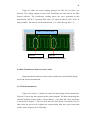
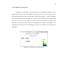
4.6 Graphical User Interface
Graphical user interface was developed as the additional indicator of the
water sensor system. The GUI displays the current water level sense by the sensor
node and transmitted to the receiver node. As shown in figure 4.13, the GUI display
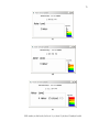
shows that on Wednesday, November 1st, 2006 at 1:09:02 PM the water indicate that
the water level was at the range of 2 meter. The level described as average and
indicates by the yellow label. This colour indicator will change accordingly to the
increments of the water level. The changes of water level indicator were enclosed in
appendix C.
Figure 4.13 GUI water level indicators.
CHAPTER 5
CONCLUSION AND SUGGESTION
5.1 Conclusion.
By the end of the day, this water sensor system has successfully achieved its
main objective. The system was successfully created with the ability to do sensing,
processing and communicate between the nodes. This system completes the main
task which is to sense the existence of water and measure several point of water
before it burst the maximum level and transmit the collected data to the receiver node
for further action. Furthermore, this water sensor system is able to perform its
operation in a real time operation with a tiny delay.
In some way, by implement this water sensor system might be helping
resident within the flood area to get prepare before the flood happen. By
implementing this system, it can as well as reducing the resident loss due to flood.
The best way to implement this system is putting the sensor at the police station or
neighborhoods center. The person who is on duty that day will inform if any danger
encounters the resident area and ask them to prepare, pack their goods and move to
safety places. Besides contribute as the flood alarm, this system also offers the other
benefit where it can be use to measure water level in the dam. It might help certain
area that facing the water supply problem.
50
5.2 Discussion and Future Work.
Implementation of TCP/IP protocol in a wireless sensor network was said to
be a hard task due to limitation of memory in the microcontroller. In a very limited
memory sizes, wireless sensor network developer should employ the gathered sensor
data as well as the protocol data into the microcontroller and finally sending the
processed data to the receiver. The processed data that sent through the network
including data header, IP address, sensor data and checksum. Different from
computer communications, sensor network didn’t have specific server to allocate and
generate its own IP address. In wireless sensor network, the developer should assign
its own IP address for each sensor or nodes depending on the network size. The
wireless sensor networks form a temporary network without any deployed
infrastructure or centralized organization. Each node that communicates each other
has an independent algorithm.
The deployment of wireless sensor network also said to be critically in term
of power efficiency. A node in wireless sensor network is not only performing as a
host, but in order to communicate each other in the network, a node also performs as
a router. Due to these reason, the node has conflicting of saving energy for its own
transmission and relaying the data to other node so the network wont break or fall
apart. This will be a challenge in deployment a large scale wireless sensor network.
This project may be enhancing by implementing a smaller size sensor
compare to the one that have been develop in this project. A smaller sensor will suit
the criteria of a wireless sensor network which is developing a tiny node that
equivalent to the coin size. Other than that, a study about power consumption should
be perform so that the nodes might work in a longer time and an effective data may
be delivered thus distortion can be avoided.
51
Furthermore, a sensor node should apply more than one sensor so that the real
sensor network can be performing with a complete protocol. Beside that, the
development of multi-hop wireless sensor network also recommended for future
work so that the many sensor node can interact each other.
Moreover, a complete protocol should be implementing in the wireless sensor
network to ensure the reliability and security of data. The data sent over the network
shouldn’t be lost or damage. If this happen if may effect the entire network and the
actually sensing data is not possible to obtain. Moreover, a central node should be
developing to gather all data from its network. This central may collect the data
from its network and store the data into a database to keep record for further
reference if anything happen in the environment.
In order to develop the entire sensor network, it requires the developer to use
a transceiver instead of using a stand alone radio frequency transmitter or receiver.
Transceiver will possible any two way communications and protocol to be embed in
the sensor network. PPP protocol can possibly be employed into the network so that
the security and reliability of data are certainly sure. Other than that, transceiver
enables both nodes to communicate each other, sending acknowledgement to ensure
data transmission and if necessary the node can resent any damage data
Finally a research on traffic delay, routing protocol and energy saving also
should be done to establish the development of wireless sensor network. The
research will enhance the wireless sensor network performance in term of traffic
delay, longer operation time for each and effective bandwidth. Other than that, the
optimal number of nodes and path can be obtaining to ensure the entire network
work efficiently.
52
REFERENCES
1. Warsuzarina Binti Mat Jubadi, Embedded TCP/IP In Sensor Nodes
SENSORNETS), Universiti Teknologi Malaysia, November 2005.
2. Forouzan, Behrouz A. (2001). Data Communications and Networking. 2nd
Edition, McGraw-Hill Higher Education.
3. William Stalling, Data and Computer Communication, 7th edition, Prentice
Hall
4. PonyProg website, URL: http://www.lancos.com/e2p/ponyprog2000.html
5. ATMEL corporation Website, URL: http://www.Atmel.com
6. Radiotronix datasheet Website, URL: www.radiotronix.com/datasheets/RCT433-AS.pdf
7. Wikipedia Website, URL: http://en.wikipedia.org/wiki/mainpage
8. Ismahayati Binti Adam, Development Of Embedded Uip Sensor Node For
Sensing Light (Transmitter), Universiti Teknologi Malaysia, May 2006.
9. answer.com, URL: www.answer.com
10. Water Level Sensor website, URL: http://www.globalw.com
53
11. I.F. Akyildiz, W. Su*, Y. Sankarasubramaniam, E. Cayirci. Wireless sensor
networks: a survey. Broadband and Wireless Networking Laboratory, School
of Electrical and Computer Engineering, Georgia Institute of Technology,
Atlanta, GA 30332, USA
12. C. C. Yee and S. P. Kumar (August 2003). Sensor Networks: Evolution,
Opportunities, and Challenges. IEEE Proceedings. Vol. 91. No. 8. pp. 12471256.
APPENDIX A
TRANSMITTER NODE SOURCE CODES
TRANSMITTER NODE MAKE FILE
55
#define FOSC 8000000// Clock Speed
#define BAUD 1200
#define baudrate (FOSC/16/BAUD-1)
#include <avr/io.h>
#include <stdio.h>
#define TX 1
void USART_INIT(unsigned int UBRR);
void USART_TX(unsigned char data);
unsigned char USART_RX(void);
void delay_1m (unsigned char i);
void ADC_INIT (void);
unsigned char ADC_READ (void);
void TMR0_INIT (void);
int main (void)
{
#if(TX==0)
#warning "TRANSMITTER"
unsigned char sen_data;
#else
#warning "RECEIVER"
unsigned char rx_data, ctr, sensor_data, chksum_;
#endif
unsigned char hdr[2] = "hf";
unsigned char add[2] = "12";
unsigned char chksum;
/* Initialize PORTC */
/*DDRC = 0xff;
/*PORTC = 0;
/* Set ID */
/* Initialize Timer0 & USART */
TMR0_INIT();
USART_INIT(baudrate);
#if(TX==0)
/* Initialize ADC */
DDRA = 0xF0;
while (1) {
sen_data = PINA;
chksum = sen_data + hdr[0] + hdr[1] + add[0] + add[1];
chksum = ~chksum;
USART_TX(hdr[0]);
USART_TX(hdr[1]);
USART_TX(add[0]);
USART_TX(add[1]);
USART_TX(sen_data);
USART_TX(chksum);
}
#else
ctr = 0;
56
DDRA = 0xff;
PORTA = 0;
while (1) {
if (UCSRA & (1<<RXC)) {
rx_data = UDR;
if (ctr < 2) {
if (rx_data == hdr[ctr]) {
ctr++;
} else {
ctr = 0;
}
} else if ((ctr > 1) && (ctr < 4)) {
if (rx_data == add[ctr - 2]) {
ctr++;
} else {
ctr = 0;
}
} else if (ctr == 4) {
sensor_data = rx_data;
ctr++;
} else if (ctr == 5) {
chksum = rx_data;
ctr++;
} else {
chksum_ = (hdr[0] + hdr[1] + add[0] +
add[1] + sensor_data + chksum);
if (chksum_ == 0xff) {
USART_TX(sensor_data);
if (sensor_data == 0x1) {
PORTA = 0x3;
} else if (sensor_data == 0x3) {
PORTA = 0x7;
} else if (sensor_data == 0x7) {
PORTA = 0xf;
} else if (sensor_data == 0xf) {
PORTA = 0x1f;
} else {
PORTA = 0x1;
}
} else {
USART_TX(0xff);
}
ctr = 0;
}
}
//if (TIFR & 0x2) {
//
TIFR |= 0x2;
//
TCNT1 = 34328;
//
//
//}
PORTA = 0xf0;
while (1);
}
/*
if (TIFR & 0x1) {
TIFR |= 0x1;
TCNT0 = 226;
57
PORTC = ~PORTC;
}*/
#endif
}
void USART_INIT(unsigned int UBRR)
{
/* Set baud rate */
UCSRA &= 0xfd;
UBRRH = (unsigned char)((UBRR)>>8);
UBRRL = (unsigned char)(UBRR);
/* Enable receiver and transmitter */
UCSRB = (1<<RXEN)|(1<<TXEN);
/* Set frame format: 8data, no parity, 1 stop bit */
UCSRC = (1<< URSEL) | (1<< UCSZ1) | (1<< UCSZ0);
}
void USART_TX(unsigned char data)
{
/* Wait for empty transmit buffer */
while ( !(UCSRA & (1<<UDRE)) ) ;
/* Start transmission */
UDR = data; // send least significant byte
}
unsigned char USART_RX(void) {
/* Wait for data to be received */
while (!(UCSRA & (1<<RXC))) ;
/* Get and return received data from buffer */
return UDR;
}
void delay_1m (unsigned char i)
{
int j;
while(i--)
{
j=11415;
// 8Mhz Exteranl Crystal(CKSEL3..0 = 1,1,1,1)
while(j--);
}
}
void ADC_INIT (void)
{
// Activate ADC with Prescaler 2
ADCSRA = 0b10000000 ;
ADMUX = 0b00100100;
}
unsigned char ADC_READ (void)
{
ADCSRA |= 0B01000000;
while (ADCSRA & _BV(ADSC) ) {}
return ADCH;
58
}
void TMR0_INIT (void)
{
//TCCR0 = 0x05;
TCCR1A = 0;
TCCR1B = 0x4;
}
59
Transmitter Node Makefile
# MCU name
MCU = atmega8535
# Output format. (can be srec, ihex, binary)
FORMAT = ihex
# Target file name (without extension).
TARGET = wlevel
# Optimization level, can be [0, 1, 2, 3, s]. 0 turns off
optimization.
# (Note: 3 is not always the best optimization level. See avr-libc
FAQ.)
OPT = s
# List C source files here. (C dependencies are automatically
generated.)
# If there is more than one source file, append them above, or
modify and
# uncomment the following:
#SRC += foo.c bar.c
# You can also wrap lines by appending a backslash to the end of the
line:
#SRC += baz.c \
#xyzzy.c
# List Assembler source files here.
# Make them always end in a capital .S. Files ending in a lowercase
.s
# will not be considered source files but generated files (assembler
# output from the compiler), and will be deleted upon "make clean"!
# Even though the DOS/Win* filesystem matches both .s and .S the
same,
# it will preserve the spelling of the filenames, and gcc itself
does
# care about how the name is spelled on its command-line.
ASRC =
# List any extra directories to look for include files here.
#
Each directory must be seperated by a space.
EXTRAINCDIRS =
# Optional compiler flags.
# -g:
generate debugging information (for GDB, or for COFF
conversion)
# -O*:
optimization level
# -f...:
tuning, see gcc manual and avr-libc documentation
# -Wall...: warning level
# -Wa,...:
tell GCC to pass this to the assembler.
#
-ahlms: create assembler listing
60
CFLAGS = -g -O$(OPT) \
-funsigned-char -funsigned-bitfields -fpack-struct -fshort-enums \
-Wall -Wstrict-prototypes \
-Wa,-adhlns=$(<:.c=.lst) \
$(patsubst %,-I%,$(EXTRAINCDIRS))
# Set a "language standard" compiler flag.
#
Unremark just one line below to set the language standard to
use.
#
gnu99 = C99 + GNU extensions. See GCC manual for more
information.
#CFLAGS += -std=c89
#CFLAGS += -std=gnu89
#CFLAGS += -std=c99
CFLAGS += -std=gnu99
# Optional assembler flags.
# -Wa,...:
tell GCC to pass this to the assembler.
# -ahlms:
create listing
# -gstabs:
have the assembler create line number information;
note that
#
for use in COFF files, additional information about
filenames
#
and function names needs to be present in the
assembler source
#
files -- see avr-libc docs [FIXME: not yet described
there]
ASFLAGS = -Wa,-adhlns=$(<:.S=.lst),-gstabs
# Optional linker flags.
# -Wl,...:
tell GCC to pass this to linker.
# -Map:
create map file
# --cref:
add cross reference to map file
LDFLAGS = -Wl,-Map=$(TARGET).map,--cref
# Additional libraries
# Minimalistic printf version
#LDFLAGS += -Wl,-u,vfprintf -lprintf_min
# Floating point printf version (requires -lm below)
#LDFLAGS += -Wl,-u,vfprintf -lprintf_flt
# -lm = math library
LDFLAGS += -lm
# Programming support using avrdude. Settings and variables.
# Programming hardware: alf avr910 avrisp bascom bsd
# dt006 pavr picoweb pony-stk200 sp12 stk200 stk500
#
61
# Type: avrdude -c ?
# to get a full listing.
#
AVRDUDE_PROGRAMMER = stk500
AVRDUDE_PORT = com1
#AVRDUDE_PORT = lpt1
# programmer connected to serial device
# programmer connected to parallel port
AVRDUDE_WRITE_FLASH = -U flash:w:$(TARGET).hex
#AVRDUDE_WRITE_EEPROM = -U eeprom:w:$(TARGET).eep
AVRDUDE_FLAGS = -p $(MCU) -P $(AVRDUDE_PORT) -c
$(AVRDUDE_PROGRAMMER)
# Uncomment the following if you want avrdude's erase cycle counter.
# Note that this counter needs to be initialized first using -Yn,
# see avrdude manual.
#AVRDUDE_ERASE += -y
# Uncomment the following if you do /not/ wish a verification to be
# performed after programming the device.
#AVRDUDE_FLAGS += -V
# Increase verbosity level. Please use this when submitting bug
# reports about avrdude. See
<http://savannah.nongnu.org/projects/avrdude>
# to submit bug reports.
#AVRDUDE_FLAGS += -v -v
# -------------------------------------------------------------------------# Define directories, if needed.
DIRAVR = c:/winavr
DIRAVRBIN = $(DIRAVR)/bin
DIRAVRUTILS = $(DIRAVR)/utils/bin
DIRINC = .
DIRLIB = $(DIRAVR)/avr/lib
# Define programs and commands.
SHELL = sh
CC = avr-gcc
OBJCOPY = avr-objcopy
OBJDUMP = avr-objdump
SIZE = avr-size
# Programming support using avrdude.
AVRDUDE = avrdude
REMOVE = rm -f
COPY = cp
62
HEXSIZE = $(SIZE) --target=$(FORMAT) $(TARGET).hex
ELFSIZE = $(SIZE) -A $(TARGET).elf
# Define Messages
# English
MSG_ERRORS_NONE = Errors: none
MSG_BEGIN = -------- begin -------MSG_END = -------- end -------MSG_SIZE_BEFORE = Size before:
MSG_SIZE_AFTER = Size after:
MSG_COFF = Converting to AVR COFF:
MSG_EXTENDED_COFF = Converting to AVR Extended COFF:
MSG_FLASH = Creating load file for Flash:
MSG_EEPROM = Creating load file for EEPROM:
MSG_EXTENDED_LISTING = Creating Extended Listing:
MSG_SYMBOL_TABLE = Creating Symbol Table:
MSG_LINKING = Linking:
MSG_COMPILING = Compiling:
MSG_ASSEMBLING = Assembling:
MSG_CLEANING = Cleaning project:
# Define all object files.
OBJ = $(SRC:.c=.o) $(ASRC:.S=.o)
# Define all listing files.
LST = $(ASRC:.S=.lst) $(SRC:.c=.lst)
# Combine all necessary flags and optional flags.
# Add target processor to flags.
ALL_CFLAGS = -mmcu=$(MCU) -I. $(CFLAGS)
ALL_ASFLAGS = -mmcu=$(MCU) -I. -x assembler-with-cpp $(ASFLAGS)
# Default target.
all: begin gccversion sizebefore $(TARGET).elf $(TARGET).hex
$(TARGET).eep \
$(TARGET).lss $(TARGET).sym sizeafter finished end
# Eye candy.
# AVR Studio 3.x does not check make's exit code but relies on
# the following magic strings to be generated by the compile job.
begin:
@echo
@echo $(MSG_BEGIN)
finished:
@echo $(MSG_ERRORS_NONE)
end:
@echo $(MSG_END)
@echo
# Display size of file.
63
sizebefore:
@if [ -f $(TARGET).elf ]; then echo; echo $(MSG_SIZE_BEFORE);
$(ELFSIZE); echo; fi
sizeafter:
@if [ -f $(TARGET).elf ]; then echo; echo $(MSG_SIZE_AFTER);
$(ELFSIZE); echo; fi
# Display compiler version information.
gccversion :
@$(CC) --version
# Convert ELF to COFF for use in debugging / simulating in
# AVR Studio or VMLAB.
COFFCONVERT=$(OBJCOPY) --debugging \
--change-section-address .data-0x800000 \
--change-section-address .bss-0x800000 \
--change-section-address .noinit-0x800000 \
--change-section-address .eeprom-0x810000
coff: $(TARGET).elf
@echo
@echo $(MSG_COFF) $(TARGET).cof
$(COFFCONVERT) -O coff-avr $< $(TARGET).cof
extcoff: $(TARGET).elf
@echo
@echo $(MSG_EXTENDED_COFF) $(TARGET).cof
$(COFFCONVERT) -O coff-ext-avr $< $(TARGET).cof
# Program the device.
program: $(TARGET).hex $(TARGET).eep
$(AVRDUDE) $(AVRDUDE_FLAGS) $(AVRDUDE_WRITE_FLASH)
$(AVRDUDE_WRITE_EEPROM)
# Create final output files (.hex, .eep) from ELF output file.
%.hex: %.elf
@echo
@echo $(MSG_FLASH) $@
$(OBJCOPY) -O $(FORMAT) -R .eeprom $< $@
%.eep: %.elf
@echo
@echo $(MSG_EEPROM) $@
-$(OBJCOPY) -j .eeprom --set-sectionflags=.eeprom="alloc,load" \
--change-section-lma .eeprom=0 -O $(FORMAT) $< $@
64
# Create extended listing file from ELF output file.
%.lss: %.elf
@echo
@echo $(MSG_EXTENDED_LISTING) $@
$(OBJDUMP) -h -S $< > $@
# Create a symbol table from ELF output file.
%.sym: %.elf
@echo
@echo $(MSG_SYMBOL_TABLE) $@
avr-nm -n $< > $@
# Link: create ELF output file from object files.
.SECONDARY : $(TARGET).elf
.PRECIOUS : $(OBJ)
%.elf: $(OBJ)
@echo
@echo $(MSG_LINKING) $@
$(CC) $(ALL_CFLAGS) $(OBJ) --output $@ $(LDFLAGS)
# Compile: create object files from C source files.
%.o : %.c
@echo
@echo $(MSG_COMPILING) $<
$(CC) -c $(ALL_CFLAGS) $< -o $@
# Compile: create assembler files from C source files.
%.s : %.c
$(CC) -S $(ALL_CFLAGS) $< -o $@
# Assemble: create object files from assembler source files.
%.o : %.S
@echo
@echo $(MSG_ASSEMBLING) $<
$(CC) -c $(ALL_ASFLAGS) $< -o $@
# Target: clean project.
clean: begin clean_list finished end
clean_list :
@echo
@echo $(MSG_CLEANING)
$(REMOVE) $(TARGET).hex
$(REMOVE) $(TARGET).eep
$(REMOVE) $(TARGET).obj
$(REMOVE) $(TARGET).cof
$(REMOVE) $(TARGET).elf
$(REMOVE) $(TARGET).map
$(REMOVE) $(TARGET).obj
$(REMOVE) $(TARGET).a90
$(REMOVE) $(TARGET).sym
65
$(REMOVE)
$(REMOVE)
$(REMOVE)
$(REMOVE)
$(REMOVE)
$(REMOVE)
$(TARGET).lnk
$(TARGET).lss
$(OBJ)
$(LST)
$(SRC:.c=.s)
$(SRC:.c=.d)
# Automatically generate C source code dependencies.
# (Code originally taken from the GNU make user manual and modified
# (See README.txt Credits).)
#
# Note that this will work with sh (bash) and sed that is shipped
with WinAVR
# (see the SHELL variable defined above).
# This may not work with other shells or other seds.
#
%.d: %.c
set -e; $(CC) -MM $(ALL_CFLAGS) $< \
| sed 's,\(.*\)\.o[ :]*,\1.o \1.d : ,g' > $@; \
[ -s $@ ] || rm -f $@
# Remove the '-' if you want to see the dependency files generated.
-include $(SRC:.c=.d)
# Listing of phony targets.
.PHONY : all begin finish end sizebefore sizeafter gccversion coff
extcoff \
clean clean_list program
APPENDIX B
RF MODULE DATA SHEET
ATMEL ATMEGA8535 BLOCK DIAGRAM
RCT-433-AS / ASB
Low-Cost SAW-stabilized surface mount
OOK RF transmitter
Embedding the wireless future..
Features
Typical Applications
•
Remote Keyless Entry (RKE)
•
Remote Lighting Controls
•
On-Site Paging
•
Asset Tracking
•
Wireless Alarm and Security Systems
•
Long Range RFID
•
Automated Resource Management
•
315/418/433.92 MHz versions
•
Low Cost
•
1.5-12V operation
•
5mA current consumption at 3V
•
Small size.
•
0dBm output power at 3V
•
4800 baud operation
Description
RCT-433-AS
The RCT-433-AS is ideal for remote control
applications where low cost and longer range are
required. The transmitter operates from a 1.5-12V
supply, making it ideal for battery-powered
applications. The transmitter employs a SAWstabilized oscillator, ensuring accurate frequency
control for best range performance. Output power
and harmonic emissions are easy to control,
making FCC and ETSI compliance easy. The
manufacturing-friendly SMT style package and lowcost make the RCT-433-AS suitable for high
volume applications. The RCT-433-ASB is suitable
for IR reflow ovens and hot air soldering.
RCT-433-ASB
Ordering Information
Frequency
433.92 MHz
433.92 MHz
Part Number
RCT-433-AS
RCT-433-ASB
Domestic and international orders:
Mouser Electronics 1-800-346-6873 (http://www.mouser.com)
Future Electronics (http://www.futureelectronics.com)
For a Radiotronix Representative in your area please visit www.radiotronix.com and visit our corporate
information page.
-i-
Document Control
Created By
Steve Montgomery
05/21/02
Engineering Review
Tom Marks
8/21/03
Marketing Review
Bryan Montgomery
8/21/03
Approved - Engineering
Tom Marks
8/21/03
Approved - Marketing
Bryan Montgomery
8/21/03
Revision History
Revision
1.1.0
1.2.0
1.3.0
1.4.0
Author
SJM
BFA
SJM
GWH
Date
05/21/02
07/30/03
8/21/03
6/7/05
Description
Document Created
Revision
Revision. Added troubleshooting and design tips.
Added RCT-433-ASB specification to datasheet.
- ii -
RCT-433-AS
Low-Cost SAW-stabilized surface mount OOK RF transmitter
© 2001,2002,2003 All Rights Reserved
Pin Out Diagram
Pin Description
Pin No.
Pin Name
1
ANT
2
GND
3
DATA
4
VCC
Description
50 ohm antenna output. The antenna port impedance affects output
power and harmonic emissions. An L-C low-pass filter may be
needed to sufficiently filter harmonic emissions.
Transmitter ground. Connect to ground plane.
Digital data input. This input is CMOS compatible and should be
driven with CMOS level inputs.
Pin 4 provides operating voltage for the transmitter. VCC should be
bypassed with a .01uF ceramic capacitor and filtered with a 4.7uF
tantalum capacitor. Noise on the power supply will degrade
transmitter noise performance.
Mechanical Drawing
0.30”
Figure 1: Mechanical Drawing of RCT-433-AS
Figure 2: Suggested Pad Layout
Figure 3: Mechanical Drawing of RCT-433-ASB
Figure 4: Suggested Pad Layout
-2-
6/7/2005
ATmega8535(L)
Overview
The ATmega8535 is a low-power CMOS 8-bit microcontroller based on the AVR
enhanced RISC architecture. By executing instructions in a single clock cycle, the
ATmega8535 achieves throughputs approaching 1 MIPS per MHz allowing the system
designer to optimize power consumption versus processing speed.
Block Diagram
Figure 2. Block Diagram
PA0 - PA7
PC0 - PC7
PORTA DRIVERS/BUFFERS
PORTC DRIVERS/BUFFERS
PORTA DIGITAL INTERFACE
PORTC DIGITAL INTERFACE
VCC
GND
AVCC
ADC
INTERFACE
MUX &
ADC
TWI
AREF
PROGRAM
COUNTER
STACK
POINTER
PROGRAM
FLASH
SRAM
TIMERS/
COUNTERS
OSCILLATOR
INTERNAL
OSCILLATOR
XTAL1
INSTRUCTION
REGISTER
GENERAL
PURPOSE
REGISTERS
WATCHDOG
TIMER
OSCILLATOR
XTAL2
X
INSTRUCTION
DECODER
Y
MCU CTRL.
& TIMING
RESET
Z
CONTROL
LINES
ALU
INTERRUPT
UNIT
AVR CPU
STATUS
REGISTER
EEPROM
PROGRAMMING
LOGIC
SPI
USART
+
-
INTERNAL
CALIBRATED
OSCILLATOR
COMP.
INTERFACE
PORTB DIGITAL INTERFACE
PORTD DIGITAL INTERFACE
PORTB DRIVERS/BUFFERS
PORTD DRIVERS/BUFFERS
PB0 - PB7
PD0 - PD7
3
2502FS–AVR–06/04
APPENDIX C
RESULT FROM GRAPHICAL USER INTERFACE
71
Result from Graphical User Interface
When the sensor did not sense any water, it considers as low water level.
Therefore the first level is assigned with blue color. The message also wills popup in the
“water level” section. Then when the sensor sense the first level of the water, the second
level in GUI will assign green color. This process will continue until the water reached
the highest level where the message “4 meter (critical) will appear on screen. The
following figures have summarized the operation of GUI for this system.
(a)
(b)
72
(c)
(d)
(e)
GUI result: (a) No level, (b) Level 1, (c) level 2, (d) level 3 and (e) level4
APPENDIX D
PONYPROG MANUAL
74
How to use PonyProg2000 for the Microrobot
AVR Products(Rev 0.3)
Contents
What is PonyProg2000?
How to install?
Preparation
How to download a program using PonyProg2000
What is PonyProg2000?
PonyProg is a serial device programmer software with a user-friendly GUI framework
available for Windows95, 98, 2000 & NT and Intel Linux. Its purpose is reading and writing
every serial device. At the moment it supports I²C Bus, Microwire, SPI EEPROM, the Atmel
AVR and Microchip PIC micro.
For more details, visit http://www.lancos.com/e2p/ponyprog2000.html
How to install?
Run the setup.exe file.
Preparation
1. Supply proper power to the (CPU) board.
2. Connect the downloading adapter to the PC printer port. Then connect the
downloading adapter and the board with the flat cable.
3. Turn on the power switch on the board. Power LED turns on (when applicable).
4. Compile the source file you want to download.
How to download a program using PonyProg2000
Run the PonyPorg2000 program.
75
Click on OK. The following window appears.
Click on OK. Select ‘Setup Æ Calibration’.
Click on Yes button. The following window appears.
Click on OK.
Select ‘Setup Æ interface Setup’ and set up as shown below (Parallel, Avr ISP I/O, LPT1)
and click on Probe. ‘Test Ok’ message appears. Click on OK. Click on OK.
76
Select the device you want. (‘Device Æ AVR micro Æ XXX’, XXX is the device you want)
Select ‘Command Æ Program Options’ and check as shown below. (Reload Files, Erase,
Write Program memory)
Click on OK.
Some devices require ‘Flash Fuse Bits Setting’ for the desired clock source setting. For
example, CKSEL3..0 bits of the ATmega8535 and Atmega8515 devices need to be set 1 to
77
select the External Crystal clock source mode. Refer to ‘Clock Options’ of the device sheet
for the detailed bit setting.
If you need to set the bits, select ‘Command Æ Security and Configuration Bits…’.
Click on Read button, uncheck the CKSEL3..0 bits and then click on Write button.
Fig 1.6 shows a ‘Security and Configuration Bits’ dialog box as an example.
Note: If the board has an AT90S-type CPU instead of ATmega-type, the setting is not
required.
Select ‘File Æ Open Program File’ and load the *.rom(or *.hex) file.
Select ‘Command Æ Program’ or press ‘Ctrl + P’ to start the downloading. If no ‘Program
Failed’ message appears, the downloading has been completed successfully.
www.microrobot.com