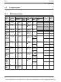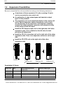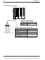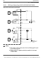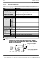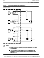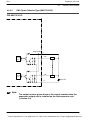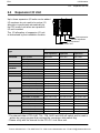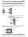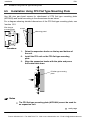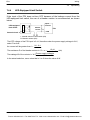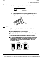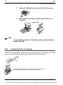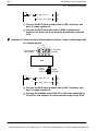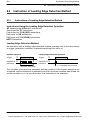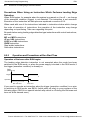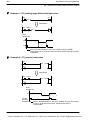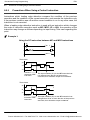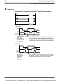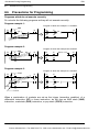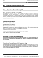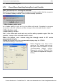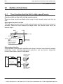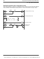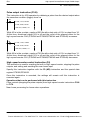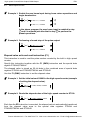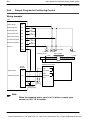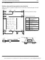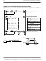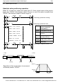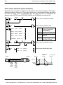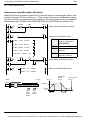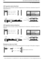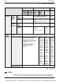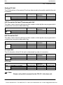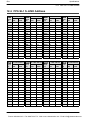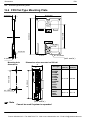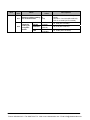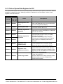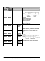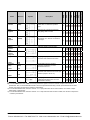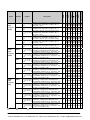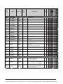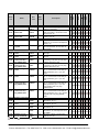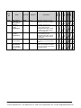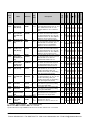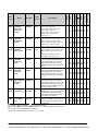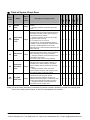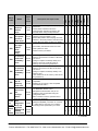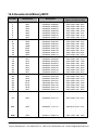
1
Phone: 800.894.0412 - Fax: 888.723.4773 - Web: www.ctiautomation.net - Email: [email protected] Safety Precautions Observe the following notices to ensure personal safety or to prevent accidents. To ensure that you use this product correctly, read this User’s Manual thoroughly before use. Make sure that you fully understand the product and information on safety. This manual uses two safety flags to indicate different levels of danger. WARNING If critical situations that could lead to user’s death or serious injury is assumed by mishandling of the product. -Always take precautions to ensure the overall safety of your system, so that the whole system remains safe in the event of failure of this product or other external factor. -Do not use this product in areas with inflammable gas. It could lead to an explosion. -Exposing this product to excessive heat or open flames could cause damage to the lithium battery or other electronic parts. -Battery may explode if mistreated. Do not recharge, disassemble or dispose of fire. CAUTION If critical situations that could lead to user’s injury or only property damage is assumed by mishandling of the product. -To prevent excessive exothermic heat or smoke generation, use this product at the values less than the maximum of the characteristics and performance that are assured in these specifications. -Do not dismantle or remodel the product. It could cause excessive exothermic heat or smoke generation. -Do not touch the terminal while turning on electricity. It could lead to an electric shock. -Use the external devices to function the emergency stop and interlock circuit. -Connect the wires or connectors securely. The loose connection could cause excessive exothermic heat or smoke generation. -Do not allow foreign matters such as liquid, flammable materials, metals to go into the inside of the product. It could cause excessive exothermic heat or smoke generation. -Do not undertake construction (such as connection and disconnection) while the power supply is on. It could lead to an electric shock. Copyright / Trademarks -This manual and its contents are copyrighted. -You may not copy this manual,in whole or part,without written consent of Panasonic Electric Works.,Ltd. -Windows and Windows NT are registered trademarks of Microsoft Corporation in the United States and/or other countries. -All other company names and product names are trademarks or registered trademarks of their respective owners. -Matsushita Electric Works,Ltd. pursues a policy of continuous improvement of the Design and performance of its products, therefore,we reserve the right to change the manual/ product without notice. BATN Phone: 800.894.0412 - Fax: 888.723.4773 - Web: www.ctiautomation.net - Email: [email protected] FP0 Introduction Introduction This manual explains hardware configurations, installation, wiring procedures, I/O allocations and maintenance. i Phone: 800.894.0412 - Fax: 888.723.4773 - Web: www.ctiautomation.net - Email: [email protected] Before You Start FP0 Before You Start Operating environment (Use the unit within the range of the general specifications when installing) Ambient temperatures:0 to +55 C Ambient humidity: 30% to 85% RH (at 25 C, non−condensing) For use in pollution Degree 2 environment. Do not use it in the following environments. − Direct sunlight − Sudden temperature changes causing condensation. − Inflammable or corrosive gas. − E−xcessive airborne dust, metal particles or saline matter. − Benzine, paint thinner, alcohol or other organic solvents or strong alkaline solutions such as mmonia or caustic soda. − Direct vibration, shock or direct drop of water. − Influence from power transmission lines, high voltage equipment, power cables, power equipment, radio transmitters, or any other equipment that would generate high switching surges. (Min.100mm or less) Static electricity Before touching the unit, always touch a grounded piece of metal in order to discharge static electricity. In dry locations, excessive static electricity can cause problems. Wiring the Power Supply to the Control Unit Use a power supply wire that is thicker than 2 mm2 (AWG14), and twist it. The unit has sufficient noise immunity against the noise generated on the power line. However, it is recommended to take measures for reducing noise such as using a isolating transformer before supplying the power. Allocate an independent wiring for each power supplying line, input/output device and operating device. If using a power supply without a protective circuit, power should be supplied through a protective element such as a fuse. Be sure to supply power to a control and an expansion units from a single power supply. Turning on/off of the power of all the units must be conducted simultaneously. ii Phone: 800.894.0412 - Fax: 888.723.4773 - Web: www.ctiautomation.net - Email: [email protected] FP0 Before You Start Power supply sequence In order to protect the power supply sequence, make sure to turn off the control unit before the input/output power supply. If the input/output power supply is turned off before the control unit, or if the control unit is not shut off momentarily, the controller detects change of input level, and might conduct an unexpected operation. Before turning ON the power When turning ON the power for the first time, be sure to take the precautions given below. When carrying out construction, check to make sure that there are no scraps of wiring, particularly conductive fragments, adhering to the unit. Verify that the power supply wiring, I/O wiring, and power supply voltage are all correct. Sufficiently tighten the installation screws and terminal screws. Set the mode switch to PROG. mode. iii Phone: 800.894.0412 - Fax: 888.723.4773 - Web: www.ctiautomation.net - Email: [email protected] Manuals To Be Used FP0 Manuals To Be Used The required manuals differ according to the units to be used. See the table below. A: Available N/A: Not available Unit type User’s manual No.ARCT1F389E Programming manual No.ARCT1F313E Manual No. FP0 Control unit A A N/A FP0 Expansion unit A A N/A FP0 Thermocouple unit A A ARCT1F366E FP0 Analog I/O unit A A ARCT1F390E FP0 A/D conversion unit A A ARCT1F321E FP0 D/A conversion unit A A ARCT1F382E FP0 CC−Link slave unit A A ARCT1F380E FP0 I/O link unit A A N/A FP0 Power supply unit A A N/A FP0 RTD unit A A ARCT1F445E − A suffix “−1” is added to the end of manual numbers when the manuals have been revised. The final number increases for every revision. − <FPWIN GR Technical Guide Book ARCT1F332E> is supplied with the standard ladder tool software FPWIN GR. − <FPWIN Pro Technical Guide Book ARCT1F405E> is supplied with the programming tool software FPWIN Pro. Key Point: The PDF versions are provided at our website. (User registration is required. Free of charge) iv Phone: 800.894.0412 - Fax: 888.723.4773 - Web: www.ctiautomation.net - Email: [email protected] FP0 Table of Contents Table of Contents Chapter 1 Overview 1.1 Components . . . . . . . . . . . . . . . . . . . . . . . . . . . . . . . . . . . . . . . . . . . . . . . . . . . . . . 1 − 3 1.1.1 FP0 Control Units . . . . . . . . . . . . . . . . . . . . . . . . . . . . . . . . . . . . . . . . . 1 − 3 1.1.2 FP0 Expansion Units . . . . . . . . . . . . . . . . . . . . . . . . . . . . . . . . . . . . . . . 1 − 4 1.1.3 Intelligent Units . . . . . . . . . . . . . . . . . . . . . . . . . . . . . . . . . . . . . . . . . . . . 1 − 5 1.1.4 Link Units . . . . . . . . . . . . . . . . . . . . . . . . . . . . . . . . . . . . . . . . . . . . . . . . 1 − 5 1.1.5 Power Supply Unit . . . . . . . . . . . . . . . . . . . . . . . . . . . . . . . . . . . . . . . . . 1 − 5 1.1.6 Options and Additional Parts . . . . . . . . . . . . . . . . . . . . . . . . . . . . . . . . 1 − 6 1.2 Expansion Possibilities . . . . . . . . . . . . . . . . . . . . . . . . . . . . . . . . . . . . . . . . . . . . . 1 − 7 1.3 Combination Possibilities . . . . . . . . . . . . . . . . . . . . . . . . . . . . . . . . . . . . . . . . . . . 1 − 8 1.3.1 Relay Output Type Units . . . . . . . . . . . . . . . . . . . . . . . . . . . . . . . . . . . . 1 − 8 1.3.2 Transistor Output Type Units . . . . . . . . . . . . . . . . . . . . . . . . . . . . . . . . 1 − 9 1.4 Programming Tools . . . . . . . . . . . . . . . . . . . . . . . . . . . . . . . . . . . . . . . . . . . . . . 1 − 10 1.4.1 Discontinued Products of Programming Tool . . . . . . . . . . . . . . . . 1 − 10 Chapter 2 Control Units 2.1 Parts and Terminology . . . . . . . . . . . . . . . . . . . . . . . . . . . . . . . . . . . . . . . . . . . . . 2 − 3 2.1.1 Control Unit Types . . . . . . . . . . . . . . . . . . . . . . . . . . . . . . . . . . . . . . . . . 2 − 4 2.1.1.1 Status Indicator LEDs . . . . . . . . . . . . . . . . . . . . . . . . . . . . 2 − 6 2.1.1.2 Mode Switch . . . . . . . . . . . . . . . . . . . . . . . . . . . . . . . . . . . 2 − 6 2.1.1.3 Tool Port . . . . . . . . . . . . . . . . . . . . . . . . . . . . . . . . . . . . . . . 2 − 6 2.2 Specifications . . . . . . . . . . . . . . . . . . . . . . . . . . . . . . . . . . . . . . . . . . . . . . . . . . . . . 2 − 7 2.2.1 General Specifications . . . . . . . . . . . . . . . . . . . . . . . . . . . . . . . . . . . . . 2 − 7 2.2.1.1 Weight . . . . . . . . . . . . . . . . . . . . . . . . . . . . . . . . . . . . . . . . . 2 − 7 2.2.1.2 Current Consumed by the Control Unit . . . . . . . . . . . . . 2 − 8 2.2.2 Performance Specifications . . . . . . . . . . . . . . . . . . . . . . . . . . . . . . . 2 − 10 2.2.3 Input Specifications . . . . . . . . . . . . . . . . . . . . . . . . . . . . . . . . . . . . . . 2 − 14 2.2.3.1 Limitations on Number of Simultaneous Input ON Points . . . . . . . . . . . . . . . . . . . . . . . . . . . . . . . . . . . . 2 − 15 2.2.4 Output Specifications . . . . . . . . . . . . . . . . . . . . . . . . . . . . . . . . . . . . 2 − 16 2.2.4.1 Relay Output Type . . . . . . . . . . . . . . . . . . . . . . . . . . . . 2 − 16 2.2.4.2 Transistor Output Type . . . . . . . . . . . . . . . . . . . . . . . . . 2 − 17 2.3 Internal Circuit Diagram . . . . . . . . . . . . . . . . . . . . . . . . . . . . . . . . . . . . . . . . . . 2.3.1 Relay Output Type (C10RS/C10CRS/C10RM/C10CRM/C14RS/ C14CRS/C14RM/C14CRM) . . . . . . . . . . . . . . . . . . . . . . . . . . . . . . . 2.3.2 Transistor Output Type . . . . . . . . . . . . . . . . . . . . . . . . . . . . . . . . . . . 2.3.2.1 NPN Open Collector Type (C16T/C16CT/C32T/C32CT/T32CT) . . . . . . . . . . . . . 2 − 18 2 − 18 2 − 19 2 − 19 v Phone: 800.894.0412 - Fax: 888.723.4773 - Web: www.ctiautomation.net - Email: [email protected] Table of Contents FP0 2.3.2.2 2.4 2.5 PNP Open Collector Type (C16P/C16CP/C32P/C32CP/T32CP) . . . . . . . . . . . . Pin Layouts . . . . . . . . . . . . . . . . . . . . . . . . . . . . . . . . . . . . . . . . . . . . . . . . . . . . 2.4.1 C10RS/C10CRS/C10RM/C10CRM . . . . . . . . . . . . . . . . . . . . . . . . 2.4.2 C14RS/C14CRS/C14RM/C14CRM . . . . . . . . . . . . . . . . . . . . . . . . 2.4.3 C16T/C16CT . . . . . . . . . . . . . . . . . . . . . . . . . . . . . . . . . . . . . . . . . . . 2.4.4 C16P/C16CP . . . . . . . . . . . . . . . . . . . . . . . . . . . . . . . . . . . . . . . . . . . 2.4.5 C32T/C32CT/T32CT . . . . . . . . . . . . . . . . . . . . . . . . . . . . . . . . . . . . . 2.4.6 C32P/C32CP/T32CP . . . . . . . . . . . . . . . . . . . . . . . . . . . . . . . . . . . . Backing Up the 10 K Step Type . . . . . . . . . . . . . . . . . . . . . . . . . . . . . . . . . . . Chapter 3 3.1 3.2 3.3 3.4 2 − 21 2 − 22 2 − 22 2 − 22 2 − 23 2 − 24 2 − 25 2 − 26 2 − 27 Expansion I/O Units Parts and Terminology . . . . . . . . . . . . . . . . . . . . . . . . . . . . . . . . . . . . . . . . . . . . . 3 − 3 3.1.1 Expansion I/O Unit Types . . . . . . . . . . . . . . . . . . . . . . . . . . . . . . . . . . . 3 − 4 Specifications . . . . . . . . . . . . . . . . . . . . . . . . . . . . . . . . . . . . . . . . . . . . . . . . . . . . . 3 − 6 3.2.1 General Specifications . . . . . . . . . . . . . . . . . . . . . . . . . . . . . . . . . . . . . 3 − 6 3.2.2 Input Specifications . . . . . . . . . . . . . . . . . . . . . . . . . . . . . . . . . . . . . . . . 3 − 6 3.2.2.1 Limitations on Number of Simultaneous Input ON Points . . . . . . . . . . . . . . . . . . . . . . . . . . . . . . . . . . . . . . 3 − 7 3.2.3 Output Specifications . . . . . . . . . . . . . . . . . . . . . . . . . . . . . . . . . . . . . . 3 − 8 3.2.3.1 Relay Output Type . . . . . . . . . . . . . . . . . . . . . . . . . . . . . . 3 − 8 3.2.3.2 Transistor Output Type . . . . . . . . . . . . . . . . . . . . . . . . . . . 3 − 9 Internal Circuit Diagram . . . . . . . . . . . . . . . . . . . . . . . . . . . . . . . . . . . . . . . . . . 3 − 10 3.3.1 Relay Output Type (E8RS/E8RM/E16RS/E16RM) . . . . . . . . . . . 3 − 10 3.3.2 Transistor Output Type . . . . . . . . . . . . . . . . . . . . . . . . . . . . . . . . . . . . 3 − 11 3.3.2.1 NPN Open Collector Type (E16T/E32T) . . . . . . . . . . . 3 − 11 3.3.2.2 PNP Open Collector Type (E16P/E32P) . . . . . . . . . . 3 − 13 3.3.3 Expansion Input Units (E8X/E16X) . . . . . . . . . . . . . . . . . . . . . . . . . 3 − 14 3.3.4 Expansion Output Units . . . . . . . . . . . . . . . . . . . . . . . . . . . . . . . . . . 3 − 15 3.3.4.1 NPN Open Collector Type (E8YT/E16YT) . . . . . . . . 3 − 15 3.3.4.2 PNP Open Collector Type (E8YP/E16YP) . . . . . . . . 3 − 17 Pin Layouts . . . . . . . . . . . . . . . . . . . . . . . . . . . . . . . . . . . . . . . . . . . . . . . . . . . . 3 − 18 3.4.1 E8RS/E8RM . . . . . . . . . . . . . . . . . . . . . . . . . . . . . . . . . . . . . . . . . . . . 3 − 18 3.4.2 E16RS/E16RM . . . . . . . . . . . . . . . . . . . . . . . . . . . . . . . . . . . . . . . . . . 3 − 19 3.4.3 E16T . . . . . . . . . . . . . . . . . . . . . . . . . . . . . . . . . . . . . . . . . . . . . . . . . . 3 − 20 3.4.4 E16P . . . . . . . . . . . . . . . . . . . . . . . . . . . . . . . . . . . . . . . . . . . . . . . . . . 3 − 21 3.4.5 E32T . . . . . . . . . . . . . . . . . . . . . . . . . . . . . . . . . . . . . . . . . . . . . . . . . . 3 − 22 3.4.6 E32P . . . . . . . . . . . . . . . . . . . . . . . . . . . . . . . . . . . . . . . . . . . . . . . . . . 3 − 23 3.4.7 E8X . . . . . . . . . . . . . . . . . . . . . . . . . . . . . . . . . . . . . . . . . . . . . . . . . . . 3 − 24 3.4.8 E16X . . . . . . . . . . . . . . . . . . . . . . . . . . . . . . . . . . . . . . . . . . . . . . . . . . 3 − 25 3.4.9 E8YT . . . . . . . . . . . . . . . . . . . . . . . . . . . . . . . . . . . . . . . . . . . . . . . . . . 3 − 26 3.4.10 E8YP . . . . . . . . . . . . . . . . . . . . . . . . . . . . . . . . . . . . . . . . . . . . . . . . . . 3 − 26 vi Phone: 800.894.0412 - Fax: 888.723.4773 - Web: www.ctiautomation.net - Email: [email protected] FP0 Table of Contents 3.4.11 3.4.12 Chapter 4 E16YT . . . . . . . . . . . . . . . . . . . . . . . . . . . . . . . . . . . . . . . . . . . . . . . . . 3 − 27 E16YP . . . . . . . . . . . . . . . . . . . . . . . . . . . . . . . . . . . . . . . . . . . . . . . . . 3 − 28 S−LINK Control Unit 4.1 Names and Functions . . . . . . . . . . . . . . . . . . . . . . . . . . . . . . . . . . . . . . . . . . . . . 4 − 3 4.2 Specifications . . . . . . . . . . . . . . . . . . . . . . . . . . . . . . . . . . . . . . . . . . . . . . . . . . . . . 4 − 5 4.2.1 General Specifications . . . . . . . . . . . . . . . . . . . . . . . . . . . . . . . . . . . . . 4 − 5 4.2.2 S−LINK Controller Specifications . . . . . . . . . . . . . . . . . . . . . . . . . . . . 4 − 6 4.3 Wiring the Power Supply . . . . . . . . . . . . . . . . . . . . . . . . . . . . . . . . . . . . . . . . . . . 4 − 7 4.3.1 Wiring to Power Supply Connector . . . . . . . . . . . . . . . . . . . . . . . . . . . 4 − 7 4.3.2 Wiring to S−LINK Terminal Block . . . . . . . . . . . . . . . . . . . . . . . . . . . . 4 − 7 4.4 Sequence of Turning on Power Supplies . . . . . . . . . . . . . . . . . . . . . . . . . . . . . 4 − 9 4.5 Operation When Power Supply is Turned On . . . . . . . . . . . . . . . . . . . . . . . . 4 − 10 4.6 S−LINK System Address Recognition . . . . . . . . . . . . . . . . . . . . . . . . . . . . . . . 4 − 11 4.6.1 Recognizing the Address . . . . . . . . . . . . . . . . . . . . . . . . . . . . . . . . . . 4 − 11 4.6.2 Address Setting of S−LINK I/O Device . . . . . . . . . . . . . . . . . . . . . . 4 − 12 4.7 Judging Errors from the Error Indicators . . . . . . . . . . . . . . . . . . . . . . . . . . . . 4 − 13 4.8 Judging Errors Address Displays . . . . . . . . . . . . . . . . . . . . . . . . . . . . . . . . . . 4 − 14 Chapter 5 I/O Allocation 5.1 I/O Number . . . . . . . . . . . . . . . . . . . . . . . . . . . . . . . . . . . . . . . . . . . . . . . . . . . . . . . 5 − 3 5.2 Control Unit . . . . . . . . . . . . . . . . . . . . . . . . . . . . . . . . . . . . . . . . . . . . . . . . . . . . . . 5 − 4 5.3 Expansion I/O Unit . . . . . . . . . . . . . . . . . . . . . . . . . . . . . . . . . . . . . . . . . . . . . . . . 5 − 5 Chapter 6 Installation 6.1 Adding Expansion Units . . . . . . . . . . . . . . . . . . . . . . . . . . . . . . . . . . . . . . . . . . . 6 − 3 6.2 Important Notes . . . . . . . . . . . . . . . . . . . . . . . . . . . . . . . . . . . . . . . . . . . . . . . . . . . 6 − 5 6.3 Attachment to DIN Rails . . . . . . . . . . . . . . . . . . . . . . . . . . . . . . . . . . . . . . . . . . . . 6 − 8 6.4 Installation Using FP0 Slim Type Mounting Plate . . . . . . . . . . . . . . . . . . . . . . 6 − 9 6.5 Installation Using FP0 Flat Type Mounting Plate . . . . . . . . . . . . . . . . . . . . . 6 − 10 Chapter 7 7.1 Wiring Safety Instructions . . . . . . . . . . . . . . . . . . . . . . . . . . . . . . . . . . . . . . . . . . . . . . . . 7 − 3 vii Phone: 800.894.0412 - Fax: 888.723.4773 - Web: www.ctiautomation.net - Email: [email protected] Table of Contents 7.1.1 7.1.2 7.1.3 7.1.4 7.1.5 FP0 Interlock Circuit . . . . . . . . . . . . . . . . . . . . . . . . . . . . . . . . . . . . . . . . . . . 7 − 3 Emergency Stop Circuit . . . . . . . . . . . . . . . . . . . . . . . . . . . . . . . . . . . . 7 − 3 Start Up Sequence . . . . . . . . . . . . . . . . . . . . . . . . . . . . . . . . . . . . . . . . 7 − 3 Momentary Power Failures . . . . . . . . . . . . . . . . . . . . . . . . . . . . . . . . . 7 − 4 Protecting Power Supply and Output Sections . . . . . . . . . . . . . . . . . 7 − 4 7.2 Wiring the Power Supply to the Control Unit . . . . . . . . . . . . . . . . . . . . . . . . . . 7 − 5 7.3 Grounding . . . . . . . . . . . . . . . . . . . . . . . . . . . . . . . . . . . . . . . . . . . . . . . . . . . . . . . . 7 − 7 7.4 Input Wiring . . . . . . . . . . . . . . . . . . . . . . . . . . . . . . . . . . . . . . . . . . . . . . . . . . . . . . 7 − 9 7.4.1 Sensors . . . . . . . . . . . . . . . . . . . . . . . . . . . . . . . . . . . . . . . . . . . . . . . . . . 7 − 9 7.4.2 LED-Equipped Reed Switch . . . . . . . . . . . . . . . . . . . . . . . . . . . . . . 7 − 10 7.4.3 Two-Wire Type Sensor . . . . . . . . . . . . . . . . . . . . . . . . . . . . . . . . . . . 7 − 10 7.4.4 LED-Equipped Limit Switch . . . . . . . . . . . . . . . . . . . . . . . . . . . . . . . . 7 − 11 7.5 Output Wiring . . . . . . . . . . . . . . . . . . . . . . . . . . . . . . . . . . . . . . . . . . . . . . . . . . . 7 − 12 7.5.1 Protective Circuit for Inductive Loads . . . . . . . . . . . . . . . . . . . . . . . 7 − 12 7.5.2 Precautions for Using Capacitive Loads . . . . . . . . . . . . . . . . . . . . 7 − 13 7.6 Wiring the Terminal Type . . . . . . . . . . . . . . . . . . . . . . . . . . . . . . . . . . . . . . . . . 7 − 14 7.7 Wiring the MOLEX Connector Type . . . . . . . . . . . . . . . . . . . . . . . . . . . . . . . . 7 − 16 7.8 Wiring the MIL Connector Type . . . . . . . . . . . . . . . . . . . . . . . . . . . . . . . . . . . 7 − 18 7.8.1 Contact Puller Pin for Rewiring . . . . . . . . . . . . . . . . . . . . . . . . . . . . 7 − 19 7.9 Wiring the RS232C Port . . . . . . . . . . . . . . . . . . . . . . . . . . . . . . . . . . . . . . . . . . 7 − 20 Chapter 8 Precautions During Programming 8.1 Use of Duplicated Output . . . . . . . . . . . . . . . . . . . . . . . . . . . . . . . . . . . . . . . . . . . 8 − 3 8.1.1 Duplicated Output . . . . . . . . . . . . . . . . . . . . . . . . . . . . . . . . . . . . . . . . . 8 − 3 8.1.2 When Output is Repeated with an OT, KP, SET, or RST Instruction . . . . . . . . . . . . . . . . . . . . . . 8 − 4 8.2 Handling BCD Data . . . . . . . . . . . . . . . . . . . . . . . . . . . . . . . . . . . . . . . . . . . . . . . 8 − 5 8.2.1 BCD Data . . . . . . . . . . . . . . . . . . . . . . . . . . . . . . . . . . . . . . . . . . . . . . . . 8 − 5 8.2.2 Handling BCD Data in the PLC . . . . . . . . . . . . . . . . . . . . . . . . . . . . . . 8 − 5 8.3 Handling Index Registers . . . . . . . . . . . . . . . . . . . . . . . . . . . . . . . . . . . . . . . . . . . 8 − 7 8.3.1 Index Registers . . . . . . . . . . . . . . . . . . . . . . . . . . . . . . . . . . . . . . . . . . . 8 − 7 8.3.2 Memory Areas Which can be Modified with Index Registers . . . . . 8 − 7 8.3.3 Example of Using an Index Register . . . . . . . . . . . . . . . . . . . . . . . . . 8 − 8 8.4 Operation Errors . . . . . . . . . . . . . . . . . . . . . . . . . . . . . . . . . . . . . . . . . . . . . . . . 8 − 10 8.4.1 Outline of Operation Errors . . . . . . . . . . . . . . . . . . . . . . . . . . . . . . . 8 − 10 8.4.2 Operation Mode When an Operation Error Occurs . . . . . . . . . . . 8 − 10 8.4.3 Dealing with Operation Errors . . . . . . . . . . . . . . . . . . . . . . . . . . . . . . 8 − 11 8.4.4 Points to Check in Program . . . . . . . . . . . . . . . . . . . . . . . . . . . . . . . 8 − 12 8.5 Instruction of Leading Edge Detection Method . . . . . . . . . . . . . . . . . . . . . . 8 − 13 8.5.1 Instructions of Leading Edge Detection Method . . . . . . . . . . . . . . 8 − 13 viii Phone: 800.894.0412 - Fax: 888.723.4773 - Web: www.ctiautomation.net - Email: [email protected] FP0 Table of Contents 8.5.2 Operation and Precautions at Run Start Time . . . . . . . . . . . . . . . 8.5.3 Precautions When Using a Control Instruction . . . . . . . . . . . . . . . 8.6 Precautions for Programming . . . . . . . . . . . . . . . . . . . . . . . . . . . . . . . . . . . . . 8.7 Rewrite Function During RUN . . . . . . . . . . . . . . . . . . . . . . . . . . . . . . . . . . . . . 8.7.1 Operation of Rewrite During RUN . . . . . . . . . . . . . . . . . . . . . . . . . . 8.7.2 Cases Where Rewriting During Run is not Possible . . . . . . . . . . 8.7.3 Procedures and Operation of Rewrite During RUN . . . . . . . . . . . 8.7.4 Changing Modes in FP Programmer II . . . . . . . . . . . . . . . . . . . . . . 8.8 Changing the Set Value of Timer/Counter During RUN . . . . . . . . . . . . . . . 8.8.1 Method of Rewriting Constant in FP Programmer II . . . . . . . . . . 8.8.2 Method of Rewriting a Value in the Set Value Area . . . . . . . . . . . 8.9 Processing During Forced Input and Output . . . . . . . . . . . . . . . . . . . . . . . . 8.10 Setting the Clock/Calendar Timer (T32CT type only) . . . . . . . . . . . . . . . . . Chapter 9 9.1 9.2 9.3 9.4 9.5 8 − 14 8 − 16 8 − 18 8 − 19 8 − 19 8 − 20 8 − 22 8 − 23 8 − 24 8 − 24 8 − 25 8 − 28 8 − 29 High−speed Counter/Pulse Output/ PWM Output Outline of Functions . . . . . . . . . . . . . . . . . . . . . . . . . . . . . . . . . . . . . . . . . . . . . . . 9 − 3 9.1.1 Three Functions that Use Built−in High−speed Counter . . . . . . . . . 9 − 3 9.1.2 Performance of Built−in High−speed Counter . . . . . . . . . . . . . . . . . . 9 − 4 Specifications and Restricted Items . . . . . . . . . . . . . . . . . . . . . . . . . . . . . . . . . . 9 − 5 9.2.1 Specifications . . . . . . . . . . . . . . . . . . . . . . . . . . . . . . . . . . . . . . . . . . . . . 9 − 5 9.2.2 Functions and Restrictions . . . . . . . . . . . . . . . . . . . . . . . . . . . . . . . . . . 9 − 7 High−speed Counter Function . . . . . . . . . . . . . . . . . . . . . . . . . . . . . . . . . . . . . . 9 − 9 9.3.1 Outline of High−speed Counter Function . . . . . . . . . . . . . . . . . . . . . . 9 − 9 9.3.2 Types of Input Modes . . . . . . . . . . . . . . . . . . . . . . . . . . . . . . . . . . . . . . 9 − 9 9.3.3 I/O Allocation . . . . . . . . . . . . . . . . . . . . . . . . . . . . . . . . . . . . . . . . . . . . 9 − 11 9.3.4 Instructions Used with High−speed Counter Function . . . . . . . . . 9 − 12 9.3.5 Sample Program . . . . . . . . . . . . . . . . . . . . . . . . . . . . . . . . . . . . . . . . 9 − 14 Pulse Output Function . . . . . . . . . . . . . . . . . . . . . . . . . . . . . . . . . . . . . . . . . . . 9 − 18 9.4.1 Outline of Pulse Output Function . . . . . . . . . . . . . . . . . . . . . . . . . . 9 − 18 9.4.2 Control Mode . . . . . . . . . . . . . . . . . . . . . . . . . . . . . . . . . . . . . . . . . . . 9 − 19 9.4.3 I/O Allocation and Wiring . . . . . . . . . . . . . . . . . . . . . . . . . . . . . . . . . 9 − 20 9.4.4 Instructions Used with Pulse Output Function . . . . . . . . . . . . . . . 9 − 22 9.4.5 Sample Program for Positioning Control . . . . . . . . . . . . . . . . . . . . 9 − 25 PWM Output Function . . . . . . . . . . . . . . . . . . . . . . . . . . . . . . . . . . . . . . . . . . . 9 − 33 9.5.1 Outline of PWM Output Function . . . . . . . . . . . . . . . . . . . . . . . . . . 9 − 33 9.5.2 Instruction Used with PWM Output Function . . . . . . . . . . . . . . . . . 9 − 33 Chapter 10 General−use Serial Communications 10.1 General−use Serial Communications Function . . . . . . . . . . . . . . . . . . . . . . 10 − 3 ix Phone: 800.894.0412 - Fax: 888.723.4773 - Web: www.ctiautomation.net - Email: [email protected] Table of Contents 10.1.1 General−use Serial Communications . . . . . . . . . . . . . . . . . . . . . . . 10.1.2 Data Transmission . . . . . . . . . . . . . . . . . . . . . . . . . . . . . . . . . . . . . . . 10.1.3 Data Reception . . . . . . . . . . . . . . . . . . . . . . . . . . . . . . . . . . . . . . . . . 10.2 System Register Settings . . . . . . . . . . . . . . . . . . . . . . . . . . . . . . . . . . . . . . . . 10.3 Operations When Using General−use Serial Communication . . . . . . . . . . 10.3.1 If “None” is Set for Start and Terminal Codes . . . . . . . . . . . . . . . . 10.3.2 If “Yes” has been Set for the Start and Terminal Codes (Start Code: STX, Terminal Code: ETX) . . . . . . . . . . . . . . . . . . . . FP0 10 − 3 10 − 3 10 − 4 10 − 5 10 − 8 10 − 8 10 − 9 Chapter 11 Self-Diagnostic and Troubleshooting 11.1 Self-Diagnostic Function . . . . . . . . . . . . . . . . . . . . . . . . . . . . . . . . . . . . . . . . . . 11 − 3 11.1.1 Allowing Duplicated Output . . . . . . . . . . . . . . . . . . . . . . . . . . . . . . . . 11 − 4 11.1.2 Continuing After an Operation Error . . . . . . . . . . . . . . . . . . . . . . . . . 11 − 4 11.2 Troubleshooting . . . . . . . . . . . . . . . . . . . . . . . . . . . . . . . . . . . . . . . . . . . . . . . . . . 11 − 5 11.2.1 ERROR/ALARM LED is Blinking . . . . . . . . . . . . . . . . . . . . . . . . . . . . 11 − 5 11.2.2 ERROR/ALARM LED is ON . . . . . . . . . . . . . . . . . . . . . . . . . . . . . . . . 11 − 7 11.2.3 All LEDs are OFF . . . . . . . . . . . . . . . . . . . . . . . . . . . . . . . . . . . . . . . . . 11 − 7 11.2.4 Diagnosing Output Malfunction . . . . . . . . . . . . . . . . . . . . . . . . . . . . . 11 − 8 11.2.5 PROTECT ERROR is Displayed . . . . . . . . . . . . . . . . . . . . . . . . . . 11 − 10 11.2.6 Program Mode does not Change to RUN . . . . . . . . . . . . . . . . . . 11 − 10 Chapter 12 Specifications 12.1 12.2 12.3 12.4 12.5 Performance Specifications . . . . . . . . . . . . . . . . . . . . . . . . . . . . . . . . . . . . . . . 12 − 3 I/O Allocation Table . . . . . . . . . . . . . . . . . . . . . . . . . . . . . . . . . . . . . . . . . . . . . . 12 − 8 Relays, Memory Areas and Constants . . . . . . . . . . . . . . . . . . . . . . . . . . . . 12 − 11 FP0−SL1 S−LINK Address . . . . . . . . . . . . . . . . . . . . . . . . . . . . . . . . . . . . . . 12 − 13 Specification: Power Supply Unit I/O Link Unit . . . . . . . . . . . . . . . . . . . . . . 12 − 14 12.5.1 FP0 Power Supply Unit (AFP0634) . . . . . . . . . . . . . . . . . . . . . . . 12 − 14 12.5.2 FP0 I/O Link Unit . . . . . . . . . . . . . . . . . . . . . . . . . . . . . . . . . . . . . . . 12 − 14 Chapter 13 Dimensions 13.1 Control Unit and Expansion I/O Unit . . . . . . . . . . . . . . . . . . . . . . . . . . . . . . . 13.1.1 FP0-C10RS/C10CRS/C14RS/C14CRS/ E8RS/E16RS . . . . . . . . . . . . . . . . . . . . . . . . . . . . . . . . . . . . . . . . . . . 13.1.2 FP0-C10RM/C10CRM/C14RM/C14CRM/ E8RM/E16RM . . . . . . . . . . . . . . . . . . . . . . . . . . . . . . . . . . . . . . . . . . 13.1.3 FP0-C16T/C16CT/C16P/C16CP/E16T/E16P/E8X/E8YT/E8YP/ E32T/E32P/E16X/E16YT/E16YP . . . . . . . . . . . . . . . . . . . . . . . . . . 13 − 3 13 − 3 13 − 3 13 − 4 x Phone: 800.894.0412 - Fax: 888.723.4773 - Web: www.ctiautomation.net - Email: [email protected] FP0 Table of Contents 13.1.4 13.1.5 FP0-C32T/C32CT/C32P/C32CP/T32CT/T32CP . . . . . . . . . . . . . 13 − 4 FP0 S−LINK Control Unit . . . . . . . . . . . . . . . . . . . . . . . . . . . . . . . . . 13 − 5 13.2 FP0 Power Supply Unit . . . . . . . . . . . . . . . . . . . . . . . . . . . . . . . . . . . . . . . . . . 13 − 5 13.3 Mounting on DIN Rail . . . . . . . . . . . . . . . . . . . . . . . . . . . . . . . . . . . . . . . . . . . . 13 − 6 13.4 FP0 Slim Type Mounting Plate . . . . . . . . . . . . . . . . . . . . . . . . . . . . . . . . . . . . 13 − 7 13.5 FP0 Flat Type Mounting Plate . . . . . . . . . . . . . . . . . . . . . . . . . . . . . . . . . . . . . 13 − 8 13.6 Cable/Adapter Specifications . . . . . . . . . . . . . . . . . . . . . . . . . . . . . . . . . . . . . 13 − 9 13.6.1 AFC8503/AFC8503S . . . . . . . . . . . . . . . . . . . . . . . . . . . . . . . . . . . . 13 − 9 13.6.2 AFC8513 . . . . . . . . . . . . . . . . . . . . . . . . . . . . . . . . . . . . . . . . . . . . . . . 13 − 9 13.6.3 AFC8521/AFC8523 (Programmer) . . . . . . . . . . . . . . . . . . . . . . . . 13 − 10 13.6.4 AFC85305/AFC8531/AFC8532 (For extending for the tool port) . . . . . . . . . . . . . . . . . . . . . . . . . . . 13 − 10 13.7 Connection (between RS232C port and PC) . . . . . . . . . . . . . . . . . . . . . . . 13 − 11 Chapter 14 Appendix 14.1 System Registers / Special Internal Relays / Special Data Registers . . . . 14 - 3 14.1.1 Table of System Registers for FP0 . . . . . . . . . . . . . . . . . . . . . . . . . . 14 - 5 14.1.2 Table of Special Internal Relays for FP0 . . . . . . . . . . . . . . . . . . . . 14 - 17 14.1.3 Table of Special Data Registers for FP0 . . . . . . . . . . . . . . . . . . . . 14 - 20 14.2 Table of Basic Instructions . . . . . . . . . . . . . . . . . . . . . . . . . . . . . . . . . . . . . . . 14 − 30 14.3 Table of High-level Instructions . . . . . . . . . . . . . . . . . . . . . . . . . . . . . . . . . . . 14 − 64 14.4 Table of Error codes . . . . . . . . . . . . . . . . . . . . . . . . . . . . . . . . . . . . . . . . . . . 14 − 124 14.5 MEWTOCOL−COM Communication Commands . . . . . . . . . . . . . . . . . . 14 − 138 14.6 Hexadecimal/Binary/BCD . . . . . . . . . . . . . . . . . . . . . . . . . . . . . . . . . . . . . . . 14 - 139 14.7 ASCII Codes . . . . . . . . . . . . . . . . . . . . . . . . . . . . . . . . . . . . . . . . . . . . . . . . . . 14 - 140 Index . . . . . . . . . . . . . . . . . . . . . . . . . . . . . . . . . . . . . . . . . . . . . . . . . . . . . . . . . . . . . . . . . . . . . . Record of changes I−1 ................................................... R−1 xi Phone: 800.894.0412 - Fax: 888.723.4773 - Web: www.ctiautomation.net - Email: [email protected] Table of Contents FP0 xii Phone: 800.894.0412 - Fax: 888.723.4773 - Web: www.ctiautomation.net - Email: [email protected] Chapter 1 Overview 1.1 Components . . . . . . . . . . . . . . . . . . . . . . . . . . . . . . . . . . . . 1 − 3 1.1.1 FP0 Control Units . . . . . . . . . . . . . . . . . . . . . . . 1 − 3 1.1.2 FP0 Expansion Units . . . . . . . . . . . . . . . . . . . . . 1 − 4 1.1.3 Intelligent Units . . . . . . . . . . . . . . . . . . . . . . . . . . 1 − 5 1.1.4 Link Units . . . . . . . . . . . . . . . . . . . . . . . . . . . . . . 1 − 5 1.1.5 Power Supply Unit . . . . . . . . . . . . . . . . . . . . . . . 1 − 5 1.1.6 Options and Additional Parts . . . . . . . . . . . . . . 1 − 6 1.2 Expansion Possibilities . . . . . . . . . . . . . . . . . . . . . . . . . . . 1 − 7 1.3 Combination Possibilities . . . . . . . . . . . . . . . . . . . . . . . . . 1 − 8 1.4 1.3.1 Relay Output Type Units . . . . . . . . . . . . . . . . . . 1 − 8 1.3.2 Transistor Output Type Units . . . . . . . . . . . . . . 1 − 9 Programming Tools . . . . . . . . . . . . . . . . . . . . . . . . . . . . 1 − 10 Phone: 800.894.0412 - Fax: 888.723.4773 - Web: www.ctiautomation.net - Email: [email protected] Overview FP0 1−2 Phone: 800.894.0412 - Fax: 888.723.4773 - Web: www.ctiautomation.net - Email: [email protected] FP0 Overview 1.1 1.1 1.1.1 Product name FP0 C10 Control Unit FP0 C10 Control Unit with RS232C port FP0 C14 Control Unit FP0 C14 Control Unit with RS232C port Components FP0 Control Units Built−in memory (Program capacuty) Specifications Number of I/O points Power supply voltage EEPROM (2 7k steps) (2.7k 10 Input: 6 Output: 4 24 V DC EEPROM (2.7k steps) 10 Input: 6 Output: 4 24 V DC EEPROM (2 7k steps) (2.7k 14 EEPROM (2.7k steps) 14 EEPROM (2.7k steps) 16 Input: 8 Output: 6 24 V DC Input: 8 Output: 6 24 V DC Input: 8 Output: 8 24 V DC FP0 C16 Control Unit FP0 C16 Control Unit with RS232C port Connection type Part No. Product No. Relay output: 2 A Terminal block FP0−C10RS AFP02123 Molex connector FP0−C10RM AFP02113 24 V DC Sink/Sourse ( common) Relay output: 2 A Terminal block FP0−C10CRS AFP02123C Molex connector FP0−C10CRM AFP02113C 24 V DC Sink/Sourse ( common) Relay output: 2 A Terminal block FP0−C14RS AFP02223 Molex connector FP0−C14RM AFP02213 24 V DC Sink/Sourse ( common) Relay output: 2 A Terminal block FP0−C14CRS AFP02223C Molex connector FP0−C14CRM AFP02213C 24 V DC Sink/Sourse ( common) Transister otuput: NPN 0.1 A MIL connector FP0−C16T AFP02343 FP0−C16P AFP02353 FP0−C16CT AFP02343C FP0−C16CP AFP02353C FP0−C32T AFP02543 FP0−C32P AFP02553 FP0−C32CT AFP02543C FP0−C32CP AFP02553C FP0−T32CT AFP02643C FP0−T32CP AFP02653C FP0−SL1 AFP02700 Input Output 24 V DC Sink/Sourse ( common) Transister otuput: PNP 0.1 A EEPROM (2.7k steps) 16 Input: 8 Output: 8 24 V DC 24 V DC Sink/Sourse ( common) Transister otuput: NPN 0.1 A MIL connector Transister otuput: PNP 0.1 A EEPROM (5k steps) 32 Input: 16 24 V DC Output: 16 FP0 C32 Control Unit FP0 C32 Control Unit with RS232C port Components 24 V DC Sink/Sourse ( common) Transister otuput: NPN 0.1 A MIL connector Transister otuput: PNP 0.1 A EEPROM (5k steps) 32 Input: 16 24 V DC Output: 16 24 V DC Sink/Sourse ( common) Transister otuput: NPN 0.1 A MIL connector Transister otuput: PNP 0.1 A FP0 T32 Control Unit with RS232C port and Clock/Calendar function EEPROM (10k steps) FP0 S−LINK Control Unit with RS232C port EEPROM (5k steps) 32 Input: 16 24 V DC Output: 16 24 V DC Sink/Sourse ( common) Transister otuput: NPN 0.1 A MIL connector Transister otuput: PNP 0.1 A 128 (S− LINK section) Input: 64 24 V DC Output: 64 (S−LINK section) — — Terminal block 1−3 Phone: 800.894.0412 - Fax: 888.723.4773 - Web: www.ctiautomation.net - Email: [email protected] Overview 1.1 FP0 Components 1.1.2 FP0 Expansion Units Specifications Product name FP0 E8 Expansion Unit Number of I/O points Power supply voltage 8 Input: 8 8 Input Output Connection type Part No. Product No. — 24 V DC Sink/Sourse ( common) — MIL connector FP0−E8X AFP03003 Input: p 4 Output: 4 24 V DC 24 V DC Sink/Sourse ( common) Relayy output: p 2A Terminal block FP0−E8RS AFP03023 Molex connector FP0−E8RM AFP03013 8 Input: 8 24 V DC — Relay output: 2 A Terminal block FP0−E8YRS AFP03020 8 Output: 8 — — Transister otuput: NPN 0.1 A MIL connector FP0−E8YT AFP03040 FP0−E8TP AFP03050 Transister otuput: PNP 0.1 A FP0 E16 Expansion U i Unit 16 Input: 16 — 24 V DC Sink/Sourse ( common) — MIL connector FP0−E16X AFP03003 16 Input: p 8 Output: 8 24 V DC 24 V DC Sink/Sourse ( common) Relayy output: p 2A Terminal block FP0−E16RS AFP03323 Molex connector FP0−E16RM AFP03313 Input: 8 Output: 8 — 24 V DC Sink/Sourse ( common)) Transister otuput: NPN 0.1 A MIL connector FP0−E16T AFP03343 FP0−E16P AFP03353 — Transister otuput: NPN 0.1 A FP0−E16YT AFP03340 FP0−E16YP AFP03350 FP0−E32T AFP03543 FP0−E32P AFP03553 16 16 Output: 16 — Transister otuput: PNP 0.1 A MIL connector Transister otuput: PNP 0.1 A FP0 E32 E Expansion i Unit 32 Input: 16 — Output: 16 24 V DC / Sink/Sourse ( common) Transister otuput: NPN 0.1 A Transister otuput: PNP 0.1 A MIL connector Notes 1) The control units and relay output type expansion units come with a power cable (part number AFP0581). (The transistor output type expansion units need no power cable.) 2) The terminal block type relay output units have 2 terminal blocks (9 pins) made by Phoenix. Use a 2.5 mm .098 inch wide screwdriver. Preferably use the specific terminal block screwdriver (part number AFP0806, Phoenix type code SZS0, 4 2.5 mm .098 inch) or equivalent. 3) The connector−type relay output units have 2 connectors made by Nihon Molex (Molex type code 51067−0900, 9 pins). Use the specific Molex connector press−fit tool (part number AFP0805, Nihon Molex type code 57189−5000) or equivalent. 4) The transistor output units have a press−fit socket for wire−pressed terminal cable and contacts. Use the press−fit tool (part number AXY52000FP) for wire−pressed terminal cable. 1−4 Phone: 800.894.0412 - Fax: 888.723.4773 - Web: www.ctiautomation.net - Email: [email protected] FP0 Overview 1.1 1.1.3 Product name Components Intelligent Units Specifications Part No. Product No. K, J, T, R thermocouple, Resolution: 0.1 C FP0−TC4 AFP0420 K, J, T, R thermocouple, Resolution: 0.1 C FP0−TC8 AFP0421 Unit for connecting FP series/RS232C interface and Ethernet Web−Server function and E−mail sending function FP−WEB AFP0610 Input specifications Number or channels Input range 2 channels : 0 to 5 V, −10 to +10 V (Resolution: 1/4000) 0 to 20 mA (Resolution: 1/4000) FP0−A21 AFP0480 Output specifications Number or channels Output range 1 channels : −10 to +10 V (Resolution: 1/4000) 0 to 20 mA (Resolution: 1/4000) FP0 A/D Converter Unit Input specifications Number or channels Input range 8 channels : 0 to 5 V, −10 to +10 V (Resolution: 1/4000) 0 to 20 mA (Resolution: 1/4000) FP0−A80 AFP0401 FP0 D/A C Converter t Unit FP0 RTD Unit Output p specifications p Number or channels Output range 4 channels : −10 10 to +10 V (Resolution: 1/4000) 4 to 20 mA (Resolution: 1/4000) FP0 TherTher mocouple l Unit FP Web− Server unit FP0 Analog I/O unit 1.1.4 Input: 6 Pt 100, Pt 1000, Ni 100 Resistance FP0−A04V AFP04121 FP0−A04I AFP04123 FP0−RTD6 AFP0430 Link Units Product name Specifications Power supply Part No. voltage Product No. FP0 CC− Link Slave Unit This unit is for making the FP0 function as a slave station of the CC−Link. Only one unit can be connected to the furthest right edge of the FP0 expansion bus. Note: Accuracy will change if an FP0 thermocouple unit is used at the same time. For details, please refer to the catalog or to the CC−Link Unit manual. 24 V DC FP0−CCLS AFP07943 FP0 I/O Link Unit This is a link unit designed to make the FP0 function as a station to MEWNET−F (remote I/O system). 24 V DC FP0−IOL AFP0732 C−NET adapter S2 type (for FP0 side) This is an RS485 adapter designed to allow use of the Computer link function for connecting to a host computer via C−NET. It comes with a 30 cm FP0 tool port cable. A power supply is not required. — — AFP15402 C−NET adapter (RS485) (for computer side) This is an RS485 adapter designed to allow use of the Computer link function for g to a network−connected PLC via C−NET from a host computer. p connecting 100 to 240 V DC — AFP8536 24 V DC — AFP8532 FP Web−Server Unit Connected with FP series PLCs, it conducts Ethernet communication, sends e−mail, and displays the PLC data on HTML pages. FP−WEB AFP0610 1.1.5 Power Supply Unit Product name Specifications Part No. Product No. FP0 Power supply unit Input voltage: 100 to 240 V AC Output: 0.7 A, 24 V DC FP0−PSA4 AFP0634 1−5 Phone: 800.894.0412 - Fax: 888.723.4773 - Web: www.ctiautomation.net - Email: [email protected] Overview 1.1 FP0 Components 1.1.6 Options and Additional Parts Product name Specifications Product No. Data clear type AFP8670 Data hold type AFP8671 Relay output type Necessary when wiring terminals block (Phoenix Contact ). AFP0806 Molex connector pressure contact tool Necessary when wiring relay output type and Molex connectors. (MOLEX: 57189−5000) AFP0805 Multi−wire connector pressure contact tool Necessary when wiring transistor output type connectors. AFP52000FP FP0 Slim 30 type mounting plate Screw−stop attachment plate for 30 mm/1.181 inch width the unit. AFP0811 (set for 10) Slim type FP0 mounting plate Screw−stop attachment plate for FP0 expansion unit. Slim model. AFP0803 (set for 10) Flat type FP0 mounting plate Screw−stop attachment plate for FP0 control unit. Flat model. AFP0804 (set for 10) Relay output Molex type I/O cable Loose wiring cable (9 leads) AWG20, with Molex socket attached at Loose−wiring one end, d 0.5 0 5 mm2, 1 set: t 2 cables bl (blue (bl & white). hit ) Length: 1 m/3.281 ft. AFP0551 (2 cable set) Length: 3 m/9.843 ft. AFP0553 (2 cable set) Transistor output type I/O cable Wire pressed terminal cable (10 leads) AWG22, 0.3 mm2 with con Wire−pressed connectors t attached tt h d att one end, d 1 set: t 2 cables bl (blue (bl & white). hit ) Length: 1 m/3.281 ft. AFP0521 (2 cable set) Length: 3 m/9.843 ft. AFP0523 (2 cable set) Flat cable connector for FPS/FP0 transistor type unit If you are using flat cable connector, request the part specified below for a connector with an asymmetrical design to prevent mistaken polarity. (10−pin) AFP0808 (4 sockets per pack) Attaches to relay output and terminal block type. Additional part AFP0802 (2 sockets per pack) Attaches to relay output and Molex connector types. Additional part AFP0801 (2 sockets per pack) Attaches to transistor output type. Additional part AFP0807 (2 sockets per pack) Attaches to FP0 various units. Additional part Length: 1 m/3.281 ft. AFP0581 (1 socket per pack) FP Memory loader Terminal screwdriver Terminal socket Molex socket Wire−press socket FP0 Power cable 1−6 Phone: 800.894.0412 - Fax: 888.723.4773 - Web: www.ctiautomation.net - Email: [email protected] FP0 Overview 1.2 1.2 Expansion Possibilities Expansion Possibilities Be sure to check that the units are added according to the following restrictions: A maximum of three expansion I/O units or analog I/O units can be connected to one control unit. A combination of relay output types and transistor output types is also possible. The expansion unit can be attached directly to the control unit easily. Special expansion cables, backplanes, and so forth, are unnecessary as the expansion unit employs a stacking system that uses expansion connector and expansion hooks on the surface of the unit itself. Install the FP0 thermocouple unit on the right side of all other expansion units. If it is installed on the left side, the total precision will deteriorate. Install the FP0 CC−Link slave unit on the right side of the other expansion units. There is no expansion connector on the right side. Install the FP0 RTD unit on the right side of the other expansion units Control unit First expansion unit Second expansion unit Third expansion unit Maximum possible expansion is with a total of 3 units Contollable I/O Points Type of control unit Control unit only When the expansion unit is the same output type as the control unit When the expansion unit is a transistor output type C10R 10 points max. 58 points max. 106 points C14R 14 points max. 62 points max. 110 points C16T/C16P 16 points max. 112 points max. 112 points C32/T32 32 points max. 128 points max. 128 points 1−7 Phone: 800.894.0412 - Fax: 888.723.4773 - Web: www.ctiautomation.net - Email: [email protected] Overview 1.3 FP0 Combination Possibilities 1.3 Combination Possibilities 1.3.1 Relay Output Type Units Total number of I/O points = 10 Output: 4 = Input: 6 Output: 6 = Input: 8 Output: 8 = Input: 6 Output: 10 = Input: 8 Output: 12 = Input: 6 = Input: 6 = Input: 8 = Input: 8 = Input: 6 = Input: 6 = Input: 8 = Input: 8 = Input: 6 = Input: 6 = Input: 8 = Input: 8 Output: 24 = Input: 6 Output: 26 = Input: 8 Output: 28 = Input: 6 Output: 30 = Input: 8 Input: 6 14 Input: 8 18 Input: 10 22 Input: 12 26 Input: 14 30 Input: 16 Output: 14 34 Input: 18 Output: 16 38 Input: 20 Output: 18 42 Input: 22 Output: 20 46 Input: 24 Output: 22 50 Input: 26 54 Input: 28 58 Input: 30 62 Input: 32 Control unit + First expansion I/O unit + Second expansion I/O unit + Third expansion I/O unit 10 Output: 4 14 Output: 6 10 Output: 4 14 Output: 6 10 Output: 4 10 Output: 4 14 Output: 6 14 Output: 6 10 Output: 4 10 Output: 4 14 Output: 6 14 Output: 6 10 Output: 4 10 Output: 4 14 Output: 6 14 Output: 6 10 Output: 4 14 Output: 6 10 Output: 4 14 Output: 6 8 + Input: 4 + Input: 4 + Input: 8 + Input: 4 + Input: 8 + Input: 4 + Input: 8 + Input: 4 + Input: 8 + Input: 4 + Input: 8 + Input: 8 + Input: 8 + Input: 8 + Input: 8 + Input: 8 + Input: 8 + Input: 8 Output: 4 8 Output: 4 16 Output: 8 8 8 + Input: 4 + Input: 4 Output: 8 + Input: 4 Output: 4 + Input: 4 Output: 8 + Input: 4 Output: 4 + Input: 4 + Input: 8 + Input: 4 + Input: 8 + Input: 4 + Input: 8 + Input: 8 + Input: 8 + Input: 8 Output: 4 Output: 4 16 Output: 8 8 Output: 4 16 8 16 8 16 Output: 8 16 Output: 8 16 Output: 8 16 Output: 8 16 Output: 8 16 Output: 8 16 Output: 8 16 Output: 8 8 Output: 4 8 Output: 4 8 Output: 4 8 + Input: 4 + Input: 4 + Input: 4 + Input: 4 + Input: 4 + Input: 4 + Input: 8 + Input: 8 Output: 4 8 Output: 4 8 Output: 4 8 Output: 4 16 Output: 8 8 Output: 4 8 Output: 4 16 Output: 8 8 Output: 4 16 Output: 8 16 Output: 8 16 Output: 8 16 Output: 8 8 Output: 4 8 Output: 4 8 Output: 4 16 Output: 8 16 Output: 8 1−8 Phone: 800.894.0412 - Fax: 888.723.4773 - Web: www.ctiautomation.net - Email: [email protected] FP0 Overview 1.3 1.3.2 Transistor Output Type Units Total number of I/O points = 16 Output: 8 = Input: 8 Output: 16 = Input: 16 Output: 16 = Input: 8 = Input: 16 Output: 16 = Input: 8 = Input: 8 = Input: 16 Output: 16 = Input: 16 Output: 16 = Input: 8 = Input: 8 = Input: 16 Output: 16 = Input: 16 Output: 16 = Input: 8 = Input: 8 = Input: 16 Output: 16 = Input: 16 Output: 16 = Input: 8 = Input: 16 Output: 16 = Input: 8 = Input: 16 Output: 16 Input: 8 32 Input: 16 48 Input: 24 Output: 24 64 Input: 32 Output: 32 80 Input: 40 Output: 40 96 Input: 48 Output: 48 112 Input: 56 Output: 56 128 Input: 64 Combination Possibilities Output: 64 Control unit + First expansion I/O unit + Second expansion I/O unit + Third expansion I/O unit 16 Output: 8 32 16 Output: 8 32 16 Output: 8 16 Output: 8 32 32 16 Output: 8 16 Output: 8 32 32 16 Output: 8 16 Output: 8 32 32 16 Output: 8 32 16 Output: 8 32 16 + Input: 8 + Input: 8 + Input: 16 Output: 16 + Input: 8 + Input: 16 Output: 16 + Input: 8 + Input: 16 Output: 16 + Input: 8 + Input: 16 Output: 16 + Input: 8 + Input: 16 Output: 16 + Input: 16 Output: 16 + Input: 16 Output: 16 + Input: 16 Output: 16 + Input: 16 Output: 16 + Input: 16 Output: 16 + Input: 16 Output: 16 + Input: 16 Output: 16 Output: 8 16 Output: 8 32 16 Output: 8 16 + Input: 8 + Input: 8 + Input: 8 + Input: 8 + Input: 8 + Input: 8 + Input: 16 Output: 16 + Input: 8 + Input: 16 Output: 16 + Input: 8 + Input: 16 Output: 16 + Input: 16 Output: 16 + Input: 16 Output: 16 + Input: 16 Output: 16 Output: 8 32 16 Output: 8 32 16 Output: 8 32 16 Output: 8 32 32 32 32 32 32 32 32 16 Output: 8 16 Output: 8 16 Output: 8 16 + Input: 8 + Input: 8 + Input: 8 + Input: 8 + Input: 8 + Input: 8 + Input: 16 Output: 16 + Input: 16 Output: 16 Output: 8 16 Output: 8 16 Output: 8 16 Output: 8 32 16 Output: 8 16 Output: 8 32 16 Output: 8 32 32 32 32 16 Output: 8 16 Output: 8 16 Output: 8 32 32 1−9 Phone: 800.894.0412 - Fax: 888.723.4773 - Web: www.ctiautomation.net - Email: [email protected] Overview 1.4 FP0 Programming Tools 1.4 Programming Tools Standard ladder diagram tool software “FPWIN GR Ver.2” Type of software OS (Operating system) Hard disc capacity Product No. FPWIN GR Ver.2 English−language menu Windows 98 Windows Me Windows 2000 Windo s XP Windows Windows Vista 40 MB or more Full type Upgraded version Small type AFPS10520 AFPS10520R AFPS11520 Notes 1) Customers who use the “FPWIN GR Ver.1” can use the “FPWIN GR Ver.2” after purchasing the upgraded version software. (The upgrade version software can be installed only when the “Ver.1.1” has been previously installed) 2) Small type version can be used for the “FP−e,” “FPΣ,” “FP0,” “FP−X,” “FP1,” and “FP−M” series. 3) Ver.2.0 can be upgraded to Ver.2.1 or later free of charge at our web site IEC61131−3−compliant programming tool software FPWIN Pro Ver.6 Type of software OS (Operating system) Hard disc capacity Product No. FPWIN GR Ver.6 English−language menu Windows 2000 Windows XP Windows Vista 100 MB or more AFPS50560 Notes 1) The small type and the upgrade version is not available for Ver. 6. 2) Ver.2.0 can be upgraded to Ver.2.1 or later free of charge at our web site Type of computer and suitable cables Connector Connector on PLC side Product No. D−Sub 9−pin Mini DIN round 5−pin AFC8503 Mini DIN round 5−pin straight type AFC8503S 1 − 10 Phone: 800.894.0412 - Fax: 888.723.4773 - Web: www.ctiautomation.net - Email: [email protected] Chapter 2 Control Units 2.1 Parts and Terminology . . . . . . . . . . . . . . . . . . . . . . . . . . . 2 − 3 2.1.1 2.2 Control Unit Types . . . . . . . . . . . . . . . . . . . . . . . 2 − 4 2.1.1.1 Status Indicator LEDs . . . . . . . . . . 2 − 6 2.1.1.2 Mode Switch . . . . . . . . . . . . . . . . . . 2 − 6 2.1.1.3 Tool Port . . . . . . . . . . . . . . . . . . . . . 2 − 6 Specifications . . . . . . . . . . . . . . . . . . . . . . . . . . . . . . . . . . . 2 − 7 2.2.1 General Specifications . . . . . . . . . . . . . . . . . . . 2 − 7 2.2.1.1 Weight . . . . . . . . . . . . . . . . . . . . . . . 2 − 7 2.2.1.2 Current Consumed by the Control Unit . . . . . . . . . . . . . . . 2 − 8 2.2.2 Performance Specifications . . . . . . . . . . . . . 2 − 10 2.2.3 Input Specifications . . . . . . . . . . . . . . . . . . . . 2 − 14 2.2.3.1 2.2.4 2.3 Limitations on Number of Simultaneous Input ON Points 2 − 15 Output Specifications . . . . . . . . . . . . . . . . . . 2 − 16 2.2.4.1 Relay Output Type . . . . . . . . . . 2 − 16 2.2.4.2 Transistor Output Type . . . . . . . 2 − 17 Internal Circuit Diagram . . . . . . . . . . . . . . . . . . . . . . . . 2 − 18 2.3.1 Relay Output Type (C10RS/C10CRS/C10RM/C10CRM/C14RS/ C14CRS/C14RM/C14CRM) . . . . . . . . . . . . . 2 − 18 2.3.2 Transistor Output Type . . . . . . . . . . . . . . . . . 2 − 19 2.3.2.1 NPN Open Collector Type (C16T/ C16CT/C32T/C32CT/T32CT) . 2 − 19 2.3.2.2 PNP Open Collector Type (C16P/ C16CP/C32P/C32CP/T32CP) . 2 − 21 next page Phone: 800.894.0412 - Fax: 888.723.4773 - Web: www.ctiautomation.net - Email: [email protected] Optional Memory FP0 2.4 2.5 Pin Layouts . . . . . . . . . . . . . . . . . . . . . . . . . . . . . . . . . . 2 − 22 2.4.1 C10RS/C10CRS/C10RM/C10CRM . . . . . . 2 − 22 2.4.2 C14RS/C14CRS/C14RM/C14CRM . . . . . . 2 − 22 2.4.3 C16T/C16CT . . . . . . . . . . . . . . . . . . . . . . . . . 2 − 23 2.4.4 C16P/C16CP . . . . . . . . . . . . . . . . . . . . . . . . . 2 − 24 2.4.5 C32T/C32CT/T32CT . . . . . . . . . . . . . . . . . . . 2 − 25 2.4.6 C32P/C32CP/T32CP . . . . . . . . . . . . . . . . . . 2 − 26 Backing Up the 10 K Step Type . . . . . . . . . . . . . . . . . 2 − 27 2−2 Phone: 800.894.0412 - Fax: 888.723.4773 - Web: www.ctiautomation.net - Email: [email protected] FP0 Optional Memory 2.1 2.1 Parts and Terminology Parts and Terminology There are sixteen different control unit types available: 1. C10RS terminal type 2. C14RS terminal type 3. C10CRS (with RS232C port) terminal type 4. C14CRS (with RS232C port) terminal type 5. C10RM connector type 6. C14RM connector type 7. C10CRM (with RS232C port) connector type 8. C14CRM (with RS232C port) connector type 9. C16T 10. C16P 11. C16CT (with RS232C port) 12. C16CP (with RS232C port) 13. C32T 14. C32P 15. C32CT (with RS232C port) 16. C32CP (with RS232C port) 17. T32CT (with RS232C port) 18. T32CP (with RS232C port) In the next sections you will find a detailed description of each control unit. 2−3 Phone: 800.894.0412 - Fax: 888.723.4773 - Web: www.ctiautomation.net - Email: [email protected] Optional Memory 2.1 FP0 Parts and Terminology 2.1.1 Control Unit Types C10RS/C14RS C10CRS/C14CRS (terminal type) 1 C10RM/C14RM C10CRM/C14CRM (connector type) 7 13 14 EXPANSION CONNECTOR 5 2 All control unit types 11 8 6 12 3 9 4 10 C16T/C16CT C16P/C16CP 15 16 C32T/C32CT C32P/C32CP T32CT/T32CP 17 Control unit with RS232C port 23 27 21 24 18 22 28 19 25 20 26 29 2−4 Phone: 800.894.0412 - Fax: 888.723.4773 - Web: www.ctiautomation.net - Email: [email protected] FP0 Optional Memory 2.1 1 7 17 23 Parts and Terminology Status indicator LEDs display the operation mode and error statuses (*section 2.1.1.1). 2 8 18 24 Mode switch changes the operation mode (*section 2.1.1.2). 3 9 19 25 Tool port (RS232C) is used to connect a programming tool (*section 2.1.1.3). 4 10 20 26 Power supply connector Supply 24 V DC. It is connected using the power supply cable (AFP0581) that comes with the unit. 5 Input terminal (9-pin) 6 Output terminal (9-pin) 7 8 9 10 The input and output terminals ( 5 and 6 ) use a terminal block socket made by Phoenix Contact Co. (product number: 1840434) (*section 7.6). 11 Input connector (9-pin) 12 Output connector (9-pin) The input and output connectors ( 11 and 51067−0900) (*section 7.7). 13 16 12 ) use a connector made by Molex Co. (product number: Expansion hook is used to secure expansion units. The hook is also used for installation on FP0 flat type mounting plate (AFP0804). Expansion connector 14 connects an expansion unit to the internal circuit of the control unit (*section 6.1). DIN rail attachment lever 15 16 17 18 19 20 allows simple attachment to a DIN rail. The lever is also used for installation on FP0 slim type mounting plate (AFP0803). 21 Input connector (10-pin) 22 Output connector (10-pin) 23 24 25 26 Use a MIL type connector for the input and output connectors ( 21 and 27 Input connectors (10-pin × 2) 28 Output connectors (10-pin × 2) Use a MIL type connector for the input and output connectors ( 27 and 29 22 ) (*section 7.8). 28 ) (*section 7.8). RS232C port Use this port to connect to devices with an RS232C port, such as an I.O.P., a bar code reader, or an image checker, enabling data input and output. (*section 7.9). 2−5 Phone: 800.894.0412 - Fax: 888.723.4773 - Web: www.ctiautomation.net - Email: [email protected] Optional Memory 2.1 FP0 Parts and Terminology 2.1.1.1 Status Indicator LEDs These LEDs display the current mode of operation or the occurrence of an error. LED Description RUN (green) Illuminates when in the RUN mode and indicates the execution of a program. It flashes during forced input/output. PROG. (green) Illuminates when in the PROG. mode and indicates that operation has stopped. ERROR/ALARM (red) Flashes when an error is detected during the self-diagnostic function. Illuminates if a hardware error occurs, or if operation slows because of the program, and the watchdog timer is activated. 2.1.1.2 Mode Switch This switch turns ON and OFF (RUN/PROG.) the operation of the FP0. The FP0 can also be turned ON and OFF by the programming tool. Switch position Operation mode RUN (upward) This sets the RUN mode. The program is executed and operation begins. PROG. (downward) This sets the PROG. mode. When performing remote switching from the programming tool, the position of the mode switch and the actual mode of operation may differ. Verify the mode with the status indicator LED. Otherwise, restart the FP0 and change the mode of operation with the mode switch. 2.1.1.3 Tool Port The tool port is used to connect a programming tool. Pin assignment 1 2 3 Pin no. Abbreviation 1 2 3 4 5 — SD (TXD) SG RD (RXD) +5V 5 4 2−6 Phone: 800.894.0412 - Fax: 888.723.4773 - Web: www.ctiautomation.net - Email: [email protected] FP0 Optional Memory 2.2 2.2 Specifications Specifications 2.2.1 General Specifications Item Description Rated operating voltage 24 V DC Operating voltage range 21.6 V to 26.4 V DC Rated current consumption 300 mA or less (*section 2.2.1.2) Allowed moment tary power off ff ti time C10/C14 5 ms at 21.6 V, 10 ms at 24 V C16/C32 T32/SL1 10 ms at 21.6 V, 10 ms at 24 V Ambient temperature 0 °C to +55 °C/32 °F to +131 °F Storage temperature −20 °C to +70 °C/−4 °F to +158 °F Ambient humidity 30 % to 85 % RH (non-condensing) Storage humidity 30 % to 85 % RH (non-condensing) Breakdown voltage 500 V AC for 1 minute between I/O terminal and power supply/ground terminal 1500 V AC for 1 minute between I/O terminal and power supply/ground terminal (relay output type only) Insulation resistance min. 100 MΩ (measured with a 500 V DC megger) between I/O terminal and ground terminal Vibration resistance 10 Hz to 55 Hz, 1 cycle/min: double amplitude of 0.75 mm/ 0.030 in., 10 min on 3 axes Shock resistance Shock of 98 m/s2 or more, 4 times on 3 axes Noise immunity 1,000 Vp-p with pulse widths 50 ns and 1 µs (based on in-house measurements) Operating condition Free from corrosive gases and excessive dust 2.2.1.1 Weight Type Weight Type Weight C10 approx. 100 g/3.53 oz SL1 approx. 120 g/4.24 oz C14 approx. 105 g/3.70 oz A21 approx. 80 g/2.82 oz C16 approx. 85 g/3.00 oz A80 approx. 90 g/3.18 oz C32 approx. 115 g/4.06 oz IOL, TC4 approx. 85 g/3.00 oz T32 approx. 125 g/4.41 oz TC8 approx. 95 g/3.35 oz E8R/E8YR approx. 90 g/3.17 oz CCLS approx. 80 g/2.82 oz E8X/E8YT/E8YP approx. 65 g/2.29 oz A04V/A04I/RTD6 approx. 75 g/2.65 oz E16RS/E16RM approx. 105 g/3.70 oz E16T/E16P/E16X/E16YT/E16YP approx. 70 g/2.47 oz E32T/E32P approx. 85 g/3.00 oz 2−7 Phone: 800.894.0412 - Fax: 888.723.4773 - Web: www.ctiautomation.net - Email: [email protected] Optional Memory 2.2 FP0 Specifications 2.2.1.2 Current Consumed by the Control Unit Unit type Control unit (The current consumed by the control unit power supply connector. If expansion units or intelligent units are added, the current is increased by the value indicated below. ) Expansion unit (The current consumed by the expansion unit power supply connector. If a unit is not listed below, it means that it has no power supply connector.) Input circuit (The current consumed by the input circuits of the various units. The value indicates the current that flows into the input circuit. ) Output circuit (The current consumed by the output circuits of the various units. The value indicates the current used to drive the output circuit. The value does not include the load current value.) — FP0−C10 100mA or less — 25.8mA or less FP0−C14 100mA or less — 34.4mA or less — FP0−C16 40mA or less — 34.4mA or less 28mA or less FP0−C32 FP0−T32 60mA or less — 68.8mA or less 52mA or less S−LINK Control unit FP0−SL1 150mA or less — — — FP0 Expansion unit FP0−E8X 10mA or less — 34.4mA or less — FP0−E8R 15mA or less 50mA or less 17.2mA or less — FP0−E8YR 10mA or less 100mA or less — — FP0−E8YT/P 15mA or less — — 24mA or less FP0−E16X 20mA or less — 68.8mA or less — FP0−E16R 20mA or less 100mA or less 34.4mA or less — FP0−E16T/P 25mA or less — 34.4mA or less 24mA or less FP0−E16YT/P 25mA or less — — 48mA or less FP0−E32T/P 40mA or less — 68.8mA or less 48mA or less FP0−A21 20mA or less 100mA or less — — FP0−A80 20mA or less 60mA or less — — FP0−A04V 20mA or less 100mA or less — — FP0−A04I 20mA or less 130mA or less — — FP0−TC4, FP0−TC8, FP0−RTD6 25mA or less — — — FP0−IOL 30mA or less 40mA or less — — FP0−CCLS 40mA or less 40mA or less — — GT01,GT01R (5VDC,RS232 C) 80mA or less — — — FP0 Control unit FP0 Intelligent unit Programmable display unit 2−8 Phone: 800.894.0412 - Fax: 888.723.4773 - Web: www.ctiautomation.net - Email: [email protected] FP0 Optional Memory 2.2 Specifications Current consumption example C14RS E32T E16T E16RS At power supply connector of expansion I/O unit FP0 E16RS Type Current consumption FP0 E16RS 100 mA At power supply connector of control unit FP Programmer II Ver. 2 Type Current consumption FP0 C14RS 100 mA FP0 E32T 40 mA FP0 E16T 25 mA FP0 E16RS 20 mA FP Programmer II Ver. 2 C−NET Adapter S2 50 mA Total current consumption 235 mA or less 2−9 Phone: 800.894.0412 - Fax: 888.723.4773 - Web: www.ctiautomation.net - Email: [email protected] Optional Memory 2.2 FP0 Specifications 2.2.2 Performance Specifications Relay output type Transistor output type S−LINK type C10RS/ C10RM/ C10CRS/ C10CRM C16T/ C16P/ C16CT/ C16CP C32T/ C32P/ C32CT/ C32CP T32C SL1 Programming method/Control method Relay symbol/Cyclic operation Controllable I/O Basic unit Total: 10 Total: 14 Total: 16 points Input: 6 Input: 8 Input: 8 Total: 32 Total: 32 Max. 128 Input: 16 Output: 16 Input: 16 Output: 16 Input: 64 Output: 64 at S−LINK block Max. 128 Max. 128 Max. 96 at Item Output: 4 Program memory Output: 6 Output: 8 With expansion Max. 58 Max. 62 Max. 112 unit 1 When configured with same output type as control unit With expansion Max. 106 Max. 110 Max. 112 unit 2 When relays and transistors are mixed Built−in memory Built in EEPROM (without battery) 2,720 steps Program capacity Numbers of i t instruction ti C14RS/ C14RM/ C14CRS/ C14CRM expansion block Max. 128 Max. 128 5,000 steps 10,000 steps 5,000 steps 83 145 Operation speed 0.9µs/step (by basic instruction) I/O refresh and base time With no expansion board: 0.3ms With expansion board(s): 0.3ms and (1 x number of expansion boards) ms Operation Relay Internal relay (R) 1,008 points (R0 to R62F) 1,008 1,008 memory points (R0 points (R0 to R62F) points to R62F) (* Note 1) Special internal 64 points (R9000 to R903F) relay (R) Timer/Counter 144 points (initial setting is 100 timer points, T0 to T99 / 44 counter points, C100 to C143 (* Note 2)) (T/C) Timer range: 1ms, 10ms, 100ms, 1s; selected by instruction Memory Data register 1,660 words (DT0 to DT1659) 6,144 16,384 6,144 area words words (DT) words (DT0 to (DT0 to (DT0 to DT6143) DT16383) DT6143) (* Note 1) Basic High-level Special data register (DT) 112 words (DT9000 to DT9111) Index register (IX, IY) Differential points (DF, DF/) 2 words Master control relay points (MCR) Number of labels (JP and LOOP) 32 points 64 labels 112 words (DT90000 to DT90111) 112 words (DT9000 to DT9111) 255 labels 64 labels Unlimited of points 2 − 10 Phone: 800.894.0412 - Fax: 888.723.4773 - Web: www.ctiautomation.net - Email: [email protected] FP0 Optional Memory 2.2 Item Relay output type Transistor output type S−LINK type C10RS/ C10RM/ C10CRS/ C10CRM C16T/ C16P/ C16CT/ C16CP SL1 C14RS/ C14RM/ C14CRS/ C14CRM C32T/ C32P/ C32CT/ C32CP Number of step ladders 128 stages Number of subroutines 16 subroutines Number of interrupt programs 7 programs (external 6 points, internal 1 point) Self-diagnosis function Such as watchdog timer, program syntax check Clock/calender function Not available Special functions Total 6 points Pulse catch input Interrupt input Specifications T32C 704 stages 128 stages (* Note 1) 100 sub16 subroutines routines 1 program (internal 1 point) Available (* Note 3) X0 to X1: 50µs X2 to X5: 100µs Not available Not available Baud rate: 300/600/1200/2400/4800/9600/19200bit/s Transmission distance: 3m/9.84ft. (Only units with an RS232C Terminal block: 3−pin, made by phoenix Contact Co. (products number: MKDS1/3−3.5) port) Communication method: Half−duplex RS232C port (* Note 4)(Non−isolated) Periodical interrupt Constant scan Password High- speed counter function (* Note 5) 0.5ms to 30s interval Available Available Counter mode: Addition/subtraction (one phase) (* Note 7) Not available − Input point number: Four channels maximum − Maximum counting speed: 10kHz maximum for all 4 channels − Input contacts used: X0: count input (ch 0) X3: count input (ch 2) X1: count input (ch 1) X4: count input (ch 3) X2: reset input (*Note 8) X5: reset input (*Note 8) − Minimum input pulse width: X0, X1 50µs, <10kHz> X3, X4 Counter mode: 100µs, <5kHz> Two−phase/individual/direction decision (two−phase) Not available − Input point number: Two channels maximum − Maximum counting speed: 2kHz maximum for all 2 channels − Input contacts used: X0: count input (ch 0) X3: count input (ch 2) X1: count input (ch 0) X4: count input (ch 2) X2: reset input X5: reset input − Minimum input pulse width: X0, X1 50µs, <10kHz> X3, X4 100µs, <5kHz> 2 − 11 Phone: 800.894.0412 - Fax: 888.723.4773 - Web: www.ctiautomation.net - Email: [email protected] Optional Memory 2.2 FP0 Specifications Item Special u c o s functions Memory backup (* Note 6, 6 12) Relay output type Transistor output type S−LINK type C10RS/ C10RM/ C10CRS/ C10CRM C16T/ C16P/ C16CT/ C16CP SL1 C14RS/ C14RM/ C14CRS/ C14CRM Pulse ou pu output f function (* Note 6,10) Output point number Output frequency Not available PWM ou pu output f function (* Note 6) Output point number Output frequency C32T/ C32P/ C32CT/ C32CP Not available Two independent points (Y0 and Y1)(no interpolation function) 40Hz to 10kHz (Y0/Y1: one−point output) 40Hz to 5kHz (Y0/Y1: two−point output) Not available Not available Not available Two points (Y0 and Y1) Not available Frequency: 0.15Hz to 38Hz, (* Note 9) Not available Not available Duty: 0.1% to 99.9% Program and system register EEPROM Operation memory Areas which are held if the power supply fails are fixed, and are retained by the EEPROM. − Number of points/words of the fixed hold areas in the various memories Counters: 4 points Internal relays: 32 points Date registers: 8 words (* Note 13) Areas which are held if the power supply fails are fixed, and are retained by the EEPROM. − Number of points/ words of the fixed hold areas in the various memories Counters: 16 points Internal relays: 128 points Date registers: 32 words (* Note 14) Backup by the F12/F13 instruction T32C Frequency: 0.15Hz to 1KHz Duty: 0.1% to 99.9% The operation memory is backed up using built−in chargeable (secondary ) battery, so the hold type memory areas can be specified using the programming tools. (* Note 11) − Memory areas which can be specified: Timers, Counters, Internal relays, Data registers Areas which are held if the power supply fails are fixed, and are retained by the EEROM. − Number of points/ words of the fixed hold areas in the various memories Counters: 16 points Internal relays: 128 points Date registers: 32 words (* Note 14) Available for all data registers Notes 1) Hold or non−hold type can be set using the system registers. 2) The proportion of timer points to counter points can be changed using a system register 5. 2 − 12 Phone: 800.894.0412 - Fax: 888.723.4773 - Web: www.ctiautomation.net - Email: [email protected] FP0 Optional Memory 2.2 Specifications Notes 3) Precision of calender timer: At 0 C/32 F, less than 139 second error per month. At 25 C/77 F, less than 72 seconds error per month. At 55 C/131 F, less than 169 seconds error per month. This accuracy is considered to be the worst fluctuation coefficient value based on fluctuations in the normal voltage of 5V and the battery backup voltage of 3V. Also, F157 and F158 (time/date addition and subtraction instructions) cannot be used. 4) When using the RS232C port for communication, we recommend using resend processing. The driver IC for the RS232C is in full conformance with EIA/TIA−232E and CCITT V.28 standards. 5) The combinations 1 phase × 2 channels and 2 phases × 1 channel are also possible for the high−speed counter. 6) The internal relay, data register, and timer/counter hold areas of the T32CT control unit (10 k step type) can be changed by the system registers. The number of points in the table is the value when the system registers are initial values. 7) The max. counting speed (10kHz) is the counting speed with a rated input voltage of 24V DC and an ambient temperature of 25°C. The counting speed (frequency) will decrease depending on the voltage and temperature. 8) If both reset inputs X0 and X1 are reset, X2 will be the reset input of X1. In the same way, for X3 and X4, X5 acts as the reset input of X4. 9) With a CPU of Ver. 1.2 or a subsequent version, the frequency will be 0.15Hz to 1kHz. 10) The maximum is 9.5kHz when the positioning control instruction (F168) is executed. 11) Precautions when using the battery backup function Secondary (chargeable) battery is used as backup battery in the FP0 T32C control unit. The battery is not charged before the unit is shipped, so please make sure that the built−in backup battery have been charged before using the unit. 12) The program, system resisters and the hold type areas (internal relay, data register and counter) are backed up by the built in EEPROM. 13) The possible number of write times by the EEPROM write instruction is 100,000 or less. 14) The possible number of write times by the EEPROM write instruction is 10,000 or less. 15) If the power supply is turned off while the P13 instruction is being executed, the data written by the P13 instruction may not be written in the EEPROM properly. Also, the area where the internal relays, data registers and timer/counter are held may not be held properly. Do not turn off the power supply while the P13 instruction is being executed. 2 − 13 Phone: 800.894.0412 - Fax: 888.723.4773 - Web: www.ctiautomation.net - Email: [email protected] Optional Memory 2.2 FP0 Specifications 2.2.3 Input Specifications Item Description Insulation method optical coupler Rated input voltage 24 V DC Rated input current approx. 4.3 mA (at 24 V DC) Input impedance approx. 5.6 kΩ Operating voltage range 21.6 to 26.4 V DC Input points per common (*Note 1) C10RM, C10CRM, C10RS, C10CRS 6 points/common C14RM, C14CRM, C14RS, C14CRS 8 points/common C16T, C16CT, C16P, C16CP 8 points/common C32T, C32CT, C32P, C32CP T32CT, T32CP 16 points/common ON voltage/ON current 19.2 V or less/3 mA or less OFF voltage/OFF current 2.4 V or more/1 mA or more OFF ↔ ON Response time 50 µs or less (at X0, X1) (* Note 2) 100 µs or less (at X2 to X5) (* Note 2) (at 24 V DC and 25 °C/66 °F) 2 ms or less (at X6 to XF) ON ↔ OFF Operating mode indicator the same as above LED Notes 1) Either positive or negative polarity is possible for the input voltage supply. 2) X0 through X5 are inputs for the high-speed counter and have a fast response time. If used as normal inputs, we recommend inserting a timer in the ladder program as chattering and noise may be interpreted as an input signal. 2 − 14 Phone: 800.894.0412 - Fax: 888.723.4773 - Web: www.ctiautomation.net - Email: [email protected] FP0 Optional Memory 2.2 2.2.3.1 Specifications Limitations on Number of Simultaneous Input ON Points Keep the number of input points per common which are simultaneously ON within the following range as determined by the temperature. FP0-C14RM/C14CRM/C14RS/C14CRS at 24 V DC Number of 8 input points per common 5 which are simultaneous 3 ON at 26.4 V DC 35/ 95 45/ 113 55/ 131 Ambient temperature (°C/°F) FP0-C16T/C16CT/C16P/C16CP at 26.4 V DC 8 Number of input points per common which are 4 simultaneous ON at 24 V DC 45/ 50/ 55/ 113 122 131 Ambient temperature (°C/°F) FP0-C32T/C32CT/C32P/C32CP/T32CT/T32CP at 26.4 V DC Number of 16 input points per common which are 8 simultaneous 6 ON at 24 V DC 23/ 31/ 73.4 87.8 55/ 131 Ambient temperature (°C/°F) 2 − 15 Phone: 800.894.0412 - Fax: 888.723.4773 - Web: www.ctiautomation.net - Email: [email protected] Optional Memory 2.2 FP0 Specifications 2.2.4 Output Specifications 2.2.4.1 Relay Output Type FP0 relay output types: C10RM, C10CRM, C10RS, C10CRS, C14RM, C14CRM, C14RS, C14CRS Item Description Output type Normally open (1 Form A) relay output Rated control capacity 2 A 250 V AC, 2 A 30 V DC (4.5 A maximum per common) (at Resistance load) Output points per common Response p time C10RM, C10CRM, C10RS, C10CRS 2 points/common +1 point/common +1 point/common C14RM, C14CRM, C14RS, C14CRS 4 points/common + 1 point/common + 1 point/common OFF → ON approx. 10 ms ON → OFF approx. 8 ms Mechanical life time 20,000,000 operations or more Electrical life time 100,000 operations or more Surge absorber None Operating mode indicator LED 2 − 16 Phone: 800.894.0412 - Fax: 888.723.4773 - Web: www.ctiautomation.net - Email: [email protected] FP0 Optional Memory 2.2 2.2.4.2 Specifications Transistor Output Type FP0 transistor output types: C16T, C16CT, C16P, C16CP, C32T, C32CT, C32P, C32CP, T32CT, T32CP Item Description Insulation method optical coupler Output type open collector Rated load voltage NPN open collector type: 5 to 24 V DC (* Note) PNP open collector type: 24 V DC Operating load voltage range NPN open collector type: 4.75 to 26.4 V DC PNP open collector type: 21.6 to 26.4 V DC Max. load current 0.1 A Max. surge current 0.3 A Output points per common co o C16T, C16CT, C16P, C16CP 8 points/common C32T, C32CT, C32P, C32CP T32CT, T32CP 16 points/common OFF state leakage current 100 µA or less ON state voltage drop 1.5 V or less External power supply for driving internal circuit Voltage 21.6 to 26.4 V DC Current Y0 and Y1: 5 mA/1 point, except Y0 and Y1: 3 mA/1 point Response p time OFF → ON 1 ms or less (Y0 and Y1 only: 50 µs or less) ON → OFF 1 ms or less (Y0 and Y1 only: 50 µs or less) Surge absorber Zener diode Operating mode indicator LED Note For NPN open collector type, able to be used with different voltages for the load voltage and the external power supply for driving the internal circuit. (+) Internal circuit Yn (−) Load External power supply for driving internal circuit (21.6 V to 26.4 V DC) Rated load voltage (5 V to 24 V DC) Ground for load voltage and for external power supply for driving internal circuit 2 − 17 Phone: 800.894.0412 - Fax: 888.723.4773 - Web: www.ctiautomation.net - Email: [email protected] Optional Memory 2.3 FP0 Internal Circuit Diagram 2.3 Internal Circuit Diagram 2.3.1 Relay Output Type (C10RS/C10CRS/C10RM/C10CRM/C14RS/C14CRS/C14RM/C14CRM) FP0-C10RS/C10CRS/C10RM/C10CRM/C14RS/C14CRS/C14RM/C14CRM Input side 5.6 kΩ Internal circuit (* Note 1) 5.6 kΩ Internal circuit X0 Xn (* Note 1) COM 24 V DC (* Note 2) Output side Y0 Load Internal circuit Yn Load Internal circuit COM Power supply Notes 1) The resistor in the control unit is 2 kΩ for X0 through X5, and 1 kΩ for X6 and X7. 2) Either positive or negative polarity is possible for the input voltage supply. 2 − 18 Phone: 800.894.0412 - Fax: 888.723.4773 - Web: www.ctiautomation.net - Email: [email protected] FP0 Optional Memory 2.3 2.3.2 Internal Circuit Diagram Transistor Output Type 2.3.2.1 NPN Open Collector Type (C16T/C16CT/C32T/C32CT/T32CT) When the load voltage and external power supply are the same This example is when the values of the rated load voltage and external power supply for driving internal circuit are the same. In this situation, there is only one power supply. FP0-C16T/C16CT/C32T/C32CT Input side 5.6 kΩ X0 Internal circuit (* Note 1) 5.6 kΩ Internal circuit Xn (* Note 1) 24 V DC (* Note 2) COM Output side (+) Internal circuit Internal circuit Y0 Yn Load Load (−) 24 V DC (External power supply and load voltage) Notes 1) The resistor in the control unit is 2 kΩ for X0 through X5, and 1 kΩ for X6 through XF. 2) Either positive or negative polarity is possible for the input voltage supply. 2 − 19 Phone: 800.894.0412 - Fax: 888.723.4773 - Web: www.ctiautomation.net - Email: [email protected] Optional Memory 2.3 FP0 Internal Circuit Diagram When the load voltage differs from the 24 V DC external power supply for the driving the internal circuit Other than 24 V DC load voltage, 5 V DC and 12 V DC and other load voltages can be connected. FP0-C16T/C16CT/C32T/C32CT/T32CT Input side 5.6 kΩ Internal circuit (* Note 1) 5.6 kΩ Internal circuit X1 (* Note 1) 5.6 kΩ Internal circuit X0 Xn (* Note 24 V DC (* Note 2) 1) COM Output side (+) Internal circuit Y0 Internal circuit Y1 Load (for 5 V ) Internal circuit Yn Load (for 24 V ) (−) Load (for 5 V ) 5V DC (Rated load voltage) 24 V DC (External power supply for driving internal circuit) Notes 1) The resistor in the control unit is 2 kΩ for X0 through X5, and 1 kΩ for X6 through XF. 2) Either positive or negative polarity is possible for the input voltage supply. 2 − 20 Phone: 800.894.0412 - Fax: 888.723.4773 - Web: www.ctiautomation.net - Email: [email protected] FP0 Optional Memory 2.3 2.3.2.2 Internal Circuit Diagram PNP Open Collector Type (C16P/C16CP/C32P/C32CP/T32CP) FP0-C16P/C16CP/C32P/C32CP/T32CP Input side 5.6 kΩ Internal circuit (* Note 1) 5.6 kΩ Internal circuit X0 Xn (* Note 1) 24 V DC (* Note 2) COM Output side Internal circuit Internal circuit (−) Y0 Yn (+) Load Load 24 V DC (Load voltage and external power supply) Notes 1) The resistor in the control unit is 2 kΩ for X0 through X5, and 1 kΩ for X6 through XF. 2) Either positive or negative polarity is possible for the input voltage supply. 2 − 21 Phone: 800.894.0412 - Fax: 888.723.4773 - Web: www.ctiautomation.net - Email: [email protected] Optional Memory 2.4 FP0 Pin Layouts 2.4 Pin Layouts 2.4.1 C10RS/C10CRS/C10RM/C10CRM Input C10RS/C10CRS X0−5 X0 X0−5 X1 C10RM/C10CRM X0 X0−5 X2 X3 X4 X5 X5 (NC) COM (NC) COM (* Note) Output Y0−3 Y0 Load Y1 (NC) Load Y2 COM Y3 COM Y0−3 Y3 COM (NC) COM 2.4.2 Y0 Y0−3 Power supply Load Load Power supply C14RS/C14CRS/C14RM/C14CRM Input X0−7 C14RS/C14CRS X0 X1 X2 X0−7 X3 X4 X5 (* Note) Y0−5 Y0 Load Y1 Y2 Y3 COM Load Load Load Y4 COM Y5 COM X0 X0−7 X7 COM X6 X7 COM Output C14RM/C14CRM Power supply Load Y0−5 Y0 Y5 COM Power supply Load Power supply Note Either positive or negative polarity is possible for the input voltage supply. 2 − 22 Phone: 800.894.0412 - Fax: 888.723.4773 - Web: www.ctiautomation.net - Email: [email protected] FP0 Optional Memory 2.4 2.4.3 Pin Layouts C16T/C16CT Input C16T/C16CT X0−7 X0 X1 X2 X3 X4 X5 X6 X7 COM COM X0 COM Α (* Note 1) Output Load Load Load Α Load Y0−7 Y0 Y1 Y2 Y3 Y4 Y5 Y6 Y7 (+) (−) X1 COM Y0 Y1 (+) (−) Load Load Load Load Notes The two COM terminals of input terminal (X0−7) are connected internally, however they should be externally connected as well. 1) Either positive or negative polarity is possible for the input voltage supply. 2 − 23 Phone: 800.894.0412 - Fax: 888.723.4773 - Web: www.ctiautomation.net - Email: [email protected] Optional Memory 2.4 FP0 Pin Layouts 2.4.4 C16P/C16CP Input C16P/C16CP X0−7 X0 X1 X2 X3 X4 X5 X6 X7 COM COM COM Α (* Note 1) Output Α Load X0 Load Load Load Y0−7 Y0 Y1 Y2 Y3 Y4 Y5 Y6 Y7 (+) (−) X1 COM Y0 Y1 (+) (−) Load Load Load Load Notes The two COM terminals of input terminal (X0−7) are connected internally, however they should be externally connected as well. 1) Either positive or negative polarity is possible for the input voltage supply. 2 − 24 Phone: 800.894.0412 - Fax: 888.723.4773 - Web: www.ctiautomation.net - Email: [email protected] FP0 Optional Memory 2.4 2.4.5 Pin Layouts C32T/C32CT/T32CT Input Input (* Note 1) Output Output (+) (+) X0 X1 C32T/C32CT X8 X9 COM COM Y0 Y1 Y8 Y9 (+) (−) (+) (−) Notes The four COM terminals of input terminals (X0−7 and X8−F) are connected internally, however they should be externally connected as well. The (+) terminals of output terminals (Y0−7) and output terminals (Y8−F) are connected internally, however they should be externally connected as well. The (−) terminals of output terminals (Y0−7) and output terminals (Y8−F) are connected internally, however they should be externally connected as well. 1) Either positive or negative polarity is possible for the input voltage supply. 2 − 25 Phone: 800.894.0412 - Fax: 888.723.4773 - Web: www.ctiautomation.net - Email: [email protected] Optional Memory 2.4 FP0 Pin Layouts 2.4.6 C32P/C32CP/T32CP Input Input X0 X1 (* Note 1) Output Output (+) (−) (+) (−) C32P/C32CP X8 X9 COM COM Y0 Y1 Y8 Y9 (+) (−) (+) (−) Notes The four COM terminals of input terminals (X0−7 and X8−F) are connected internally, however they should be externally connected as well. The (+) terminals of output terminals (Y0−7) and output terminals (Y8−F) are connected internally, however they should be externally connected as well. The (−) terminals of output terminals (Y0−7) and output terminals (Y8−F) are connected internally, however they should be externally connected as well. 1) Either positive or negative polarity is possible for the input voltage supply. 2 − 26 Phone: 800.894.0412 - Fax: 888.723.4773 - Web: www.ctiautomation.net - Email: [email protected] FP0 Optional Memory 2.5 2.5 Backing Up the 10 K Step Type Backing Up the 10 K Step Type Recharging the internal backup battery A secondary battery (rechargeable type) is used as the backup battery in the control unit (10 K step type). When shipped, this battery is not charged; therefore, please make sure it is sufficiently charged before using. Recharging is automatic when DC power is supplied. When backup is possible of operation memory Relationship between recharging time and backup time The number of days for the backup time changes with the proportion of recharging time. Please use the graph below to verify the number of days for the backup time. Relationship between recharging time and backup time 100 % B a c k u p t i m e 60 % 80 % 40day(25 ℃) 50day(25 ℃) 30 day(25℃ ) 20 % 10 day(25 ℃) 0 8 16 24 48 72 Recharging time (h) Number of days for backup depending on ambient temperature The number of days for the backup differs, as shown in the table below, when recharging is done for 72 hours at a certain ambient temperature. Ambient temperature Number of days for backup time 70 C Approx. 14 days 25 C Approx. 50 days −20 C Approx. 25 days 2 − 27 Phone: 800.894.0412 - Fax: 888.723.4773 - Web: www.ctiautomation.net - Email: [email protected] Optional Memory 2.5 FP0 Backing Up the 10 K Step Type Predicted life of internal backup battery When the control unit is on (when power is supplied) the internal backup battery life will differ depending on the ambient temperature. Refer to the table below to predict the life of the internal backup battery. Note: When the control unit is off (when power is not supplied), temperature has almost no effect on the battery life. Ambient temperature Internal backup battery life 55 C Approx. 430 days (approx. 1 year) 45 C Approx. 1,200 days (approx. 3 years) 40 C Approx. 2,100 days (approx. 6 years) 35 C Approx. 3,300 days (approx. 9 years) 34 C and less Approx. 10 years Range of backup possible with the internal backup battery − The range that the user specifies with the programming tool from among the computation memories given below, will become the holding backup area. 1) Timer/counter (T/C) 2) Internal relay (R) 3) Data register (DT) 4) Step ladder − If the user does not make a designation, the default setting range will become the backup holding area. − The clock/calendar timer value is also backed up. − The program and system registers are held in EEPROM with no relation to the internal backup battery. Handling of the internal backup battery It is not possible to replace the internal backup battery when it has been exhausted or has exceeded its life span. Cautions regarding the backup of data − The clock/calendar timer value is backed up by the secondary battery. − Begin use only after the secondary battery has been sufficiently charged. For reference To read and use the initial settings data when starting operation, you can also write the data to EEPROM by using the F12 EEPROM read instruction and the F13 EEPROM write instruction. If the power supply is turned off while the P13 instruction is being executed, data may not be written in the EEPROM properly. Also, the area where the internal relays, data registers and timer/counter are held may not be held properly. Do not turn off the power supply while the P13 instruction is being executed. 2 − 28 Phone: 800.894.0412 - Fax: 888.723.4773 - Web: www.ctiautomation.net - Email: [email protected] Chapter 3 Expansion I/O Units 3.1 Parts and Terminology . . . . . . . . . . . . . . . . . . . . . . . . . . . 3 − 3 3.1.1 3.2 Expansion I/O Unit Types . . . . . . . . . . . . . . . . . 3 − 4 Specifications . . . . . . . . . . . . . . . . . . . . . . . . . . . . . . . . . . . 3 − 6 3.2.1 General Specifications . . . . . . . . . . . . . . . . . . . 3 − 6 3.2.2 Input Specifications . . . . . . . . . . . . . . . . . . . . . . 3 − 6 3.2.2.1 3.2.3 3.3 Limitations on Number of Simultaneous Input ON Points . . 3 − 7 Output Specifications . . . . . . . . . . . . . . . . . . . . 3 − 8 3.2.3.1 Relay Output Type . . . . . . . . . . . . 3 − 8 3.2.3.2 Transistor Output Type . . . . . . . . . 3 − 9 Internal Circuit Diagram . . . . . . . . . . . . . . . . . . . . . . . . 3 − 10 3.3.1 Relay Output Type (E8RS/E8RM/E16RS/E16RM) 3 − 10 3.3.2 Transistor Output Type . . . . . . . . . . . . . . . . . . 3 − 11 3.3.2.1 NPN Open Collector Type (E16T/E32T) . . . . . . . . . . . . . . . . . 3 − 11 3.3.2.2 PNP Open Collector Type (E16P/E32P) . . . . . . . . . . . . . . . 3 − 13 3.3.3 Expansion Input Units (E8X/E16X) . . . . . . . 3 − 14 3.3.4 Expansion Output Units . . . . . . . . . . . . . . . . 3 − 15 3.3.4.1 NPN Open Collector Type (E8YT/E16YT) . . . . . . . . . . . . . . 3 − 15 3.3.4.2 PNP Open Collector Type (E8YP/E16YP) . . . . . . . . . . . . . . 3 − 17 next page Phone: 800.894.0412 - Fax: 888.723.4773 - Web: www.ctiautomation.net - Email: [email protected] Expansion I/O Units FP0 3.4 Pin Layouts . . . . . . . . . . . . . . . . . . . . . . . . . . . . . . . . . . 3 − 18 3.4.1 E8RS/E8RM . . . . . . . . . . . . . . . . . . . . . . . . . . 3 − 18 3.4.2 E16RS/E16RM . . . . . . . . . . . . . . . . . . . . . . . . 3 − 19 3.4.3 E16T . . . . . . . . . . . . . . . . . . . . . . . . . . . . . . . . 3 − 20 3.4.4 E16P . . . . . . . . . . . . . . . . . . . . . . . . . . . . . . . . 3 − 21 3.4.5 E32T . . . . . . . . . . . . . . . . . . . . . . . . . . . . . . . . 3 − 22 3.4.6 E32P . . . . . . . . . . . . . . . . . . . . . . . . . . . . . . . . 3 − 23 3.4.7 E8X 3.4.8 E16X . . . . . . . . . . . . . . . . . . . . . . . . . . . . . . . . 3 − 25 3.4.9 E8YT . . . . . . . . . . . . . . . . . . . . . . . . . . . . . . . . 3 − 26 3.4.10 E8YP . . . . . . . . . . . . . . . . . . . . . . . . . . . . . . . . 3 − 26 3.4.11 E16YT . . . . . . . . . . . . . . . . . . . . . . . . . . . . . . . 3 − 27 3.4.12 E16YP . . . . . . . . . . . . . . . . . . . . . . . . . . . . . . . 3 − 28 . . . . . . . . . . . . . . . . . . . . . . . . . . . . . . . . 3 − 24 3−2 Phone: 800.894.0412 - Fax: 888.723.4773 - Web: www.ctiautomation.net - Email: [email protected] FP0 Expansion I/O Units 3.1 3.1 Parts and Terminology Parts and Terminology There are fourteen different expansion I/O unit types available: 1. E8RS terminal type 2. E16RS terminal type 3. E8RM connector type 4. E16RM connector type 5. E16T 6. E16P 7. E32T 8. E32P 9. E8X input type 10. E16X input type 11. E8YT output type 12. E8YP output type 13. E16YT output type 14. E16YP output type In the next sections you will find a detailed description of each expansion I/O unit. 3−3 Phone: 800.894.0412 - Fax: 888.723.4773 - Web: www.ctiautomation.net - Email: [email protected] Expansion I/O Units 3.1 FP0 Parts and Terminology 3.1.1 Expansion I/O Unit Types E8RS/E16RS (terminal type) 1 E8RM/E16RM (connector type) E32T/E32P E16T/E16P 2 5 7 9 3 6 8 10 4 E8X 11 E16YT/E16YP E8YT/E8YP E16X 12 13 14 All expansion I/O unit types 15 16 17 18 3−4 Phone: 800.894.0412 - Fax: 888.723.4773 - Web: www.ctiautomation.net - Email: [email protected] FP0 Expansion I/O Units 3.1 1 4 Parts and Terminology Power supply connector Supply 24 V DC. It is connected using the power supply cable (AFP0581) that comes with the unit. 2 Input terminal (9-pin) 3 Output terminal (9-pin) 4 The input and output terminals ( 2 and 3 ) use a terminal block socket made by Phoenix Contact Co. (product number: 1840434) (*section 7.6). 5 Input connector (9-pin) 6 Output connector (9-pin) The input and output connectors ( 5 and number: 51067-0900) (*section 7.7). 7 11 ) use a connector made by Molex Japan Co. (product Input connector (10-pin) 8 13 Output connector (10-pin) 9 12 Input connector (10-pin × 2) 10 14 6 Output connector (10-pin × 2) 11 12 13 14 Use a MIL type connector for the input and output connectors ( 7 to 15 18 14 ) (*section 7.8). Expansion hook is used to secure expansion units. 16 Expansion connector connects an expansion unit to the internal circuit of the expansion I/O unit (*section 6.1). 17 DIN rail attachment lever 18 allows simple attachment to a DIN rail. The lever is also used for installation on FP0 slim type mounting plate (AFP0803). 3−5 Phone: 800.894.0412 - Fax: 888.723.4773 - Web: www.ctiautomation.net - Email: [email protected] Expansion I/O Units 3.2 FP0 Specifications 3.2 Specifications 3.2.1 General Specifications For more details on the general specifications, refer to section 2.2.1. 3.2.2 Input Specifications Item Description Insulation method optical coupler Rated input voltage 24 V DC Rated input current approx. 4.3 mA (at 24 V DC) Input impedance approx. 5.6 kΩ Operating voltage range 21.6 to 26.4 V DC Input points pe co o per common (* Note) E8RS, 4 points/common E8RM E16RS, 8 points/common E16RM, E16T, E16P, E8X E32T, E32P, 16 points/common E16X ON voltage/ON current 19.2 V or less/3 mA or less OFF voltage/OFF current 2.4 V or more/1 mA or more Response time OFF ↔ ON 2 ms or less (at 24 V DC and ON ↔ OFF the same as above 25 °C/66 °F) Operating mode indicator LED Note Either positive or negative polarity is possible for the input voltage supply. 3−6 Phone: 800.894.0412 - Fax: 888.723.4773 - Web: www.ctiautomation.net - Email: [email protected] FP0 Expansion I/O Units 3.2 3.2.2.1 Specifications Limitations on Number of Simultaneous Input ON Points Keep the number of input points per common which are simultaneously ON within the following range as determined by the temperature. FP0-E16RS/E16RM at 24 V DC at 26.4 V DC Number of 8 input points per common 6 which are simultaneous ON 47/ 55/ 116.6 131 Ambient temperature (°C/°F) FP0-E16T/E16P/E8X at 26.4 V DC Number of 8 input points per common 5 which are simultaneous 4 ON at 24 V DC 34/ 43/ 55/ 93.2 109.4 131 Ambient temperature (°C/°F) FP0-E32T/E32P/E16X Number of 16 input points per common which are 9 simultaneous 8 ON at 26.4 V DC at 24 V DC 26/ 34/ 78.8 93.2 55/ 131 Ambient temperature (°C/°F) 3−7 Phone: 800.894.0412 - Fax: 888.723.4773 - Web: www.ctiautomation.net - Email: [email protected] Expansion I/O Units 3.2 FP0 Specifications 3.2.3 3.2.3.1 Output Specifications Relay Output Type FP0 relay output types: E8RS, E8RM, E16RS, and E16RM Item Description Output type Normally open (1 Form A) relay output Rated control capacity 2 A 250 V AC, 2 A 30 V DC (4.5 A maximum per common) (at Resistance load) 4 points/common Output points pe co o per common Response p time E8RS, E8RM E16RS, 8 points/common E16RM OFF ↔ ON approx. 10 ms ON ↔ OFF approx. 8 ms Mechanical life time 20,000,000 operations or more Electrical life time 100,000 operations or more Surge absorber None Operating mode indicator LED 3−8 Phone: 800.894.0412 - Fax: 888.723.4773 - Web: www.ctiautomation.net - Email: [email protected] FP0 Expansion I/O Units 3.2 3.2.3.2 Specifications Transistor Output Type FP0 transistor output types: E16T, E16P, E32T, E32P, E8YT, E8YP, E16YT, E16YP Item Description Insulation method optical coupler Output type open collector Rated load voltage Operating load voltage range Max. load current NPN open collector type: 5 to 24 V DC (* Note) PNP open collector type: 24 V DC NPN open collector type: 4.75 to 26.4 V DC PNP open collector type: 21.6 to 26.4 V DC 0.1 A Max. surge current 0.3 A Output points per common E16T, E16P, E8YT, E8YP 8 points/common E32T, E32P, E16YT, E16YP 16 points/common OFF state leakage current 100 µA or less ON state voltage drop 1.5 V or less 21.6 to 26.4 V DC External power Voltage supply for driving internal Current Y0 and Y1: 5 mA/1 point, except Y0 and Y1: 3 mA/1 point circuit Response p time OFF → ON 1 ms or less (Y0 and Y1 only: 50 µs or less) ON → OFF 1 ms or less (Y0 and Y1 only: 50 µs or less) Surge absorber Zener diode Operating mode indicator LED Note For NPN open collector type, able to be used with different voltages for the load voltage and the external power supply for driving the internal circuit. (+) Internal circuit Yn (−) Load External power supply for driving internal circuit (21.6 V to 26.4 V DC) Rated load voltage (5 V to 24 V DC) Ground for load voltage and for external power supply for driving internal circuit 3−9 Phone: 800.894.0412 - Fax: 888.723.4773 - Web: www.ctiautomation.net - Email: [email protected] Expansion I/O Units 3.3 FP0 Internal Circuit Diagram 3.3 Internal Circuit Diagram 3.3.1 Relay Output Type (E8RS/E8RM/E16RS/E16RM) FP0-E8RS/E8RM/E16RS/E16RM Input side 5.6 kΩ Internal circuit 1 kΩ 5.6 kΩ Internal circuit X20 X2n 1 kΩ COM 24 V DC (* Note) Output side Y20 Load Internal circuit Y2n Load Internal circuit COM Power supply Notes Either positive or negative polarity is possible for the input voltage supply. The I/O number given above is the I/O number when the expansion I/O unit is installed as the first expansion unit (*section 5.3). 3 − 10 Phone: 800.894.0412 - Fax: 888.723.4773 - Web: www.ctiautomation.net - Email: [email protected] FP0 Expansion I/O Units 3.3 3.3.2 Internal Circuit Diagram Transistor Output Type 3.3.2.1 NPN Open Collector Type (E16T/E32T) When the load voltage and external power supply are the same This example is when the values of the rated load voltage and external power supply for driving internal circuit are the same. In this situation, there is only one power supply. FP0-E16T/E32T Input side 5.6 kΩ Internal circuit 1 kΩ 5.6 kΩ Internal circuit X20 X2n 1 kΩ 24 V DC (* Note) COM Output side (+) Internal circuit Internal circuit Y20 Y2n Load Load (−) 24 V DC (External power supply and load voltage) Notes Either positive or negative polarity is possible for the input voltage supply. The I/O number given above is the I/O number when the expansion I/O unit is installed as the first expansion unit (*section 5.3). 3 − 11 Phone: 800.894.0412 - Fax: 888.723.4773 - Web: www.ctiautomation.net - Email: [email protected] Expansion I/O Units 3.3 FP0 Internal Circuit Diagram When the load voltage differs from the 24 V DC external power supply for the driving the internal circuit Other than 24 V DC load voltage, 5 V DC and 12 V DC and other load voltages can be connected. FP0-E16T/E32T 5.6 kΩ Internal circuit 1 kΩ 5.6 kΩ Internal circuit X21 1 kΩ 5.6 kΩ Internal circuit X20 X2n 24 V DC (* Note) 1 kΩ COM (+) Internal circuit Y20 Load (for 5 V ) Internal circuit Y21 Load (for 5 V ) Internal circuit Y2n Load (for 24 V ) (−) 5V DC (Rated load voltage) 24 V DC (External power supply for driving internal circuit) Notes Either positive or negative polarity is possible for the input voltage supply. The I/O number given above is the I/O number when the expansion I/O unit is installed as the first expansion unit (*section 5.3). 3 − 12 Phone: 800.894.0412 - Fax: 888.723.4773 - Web: www.ctiautomation.net - Email: [email protected] FP0 Expansion I/O Units 3.3 3.3.2.2 Internal Circuit Diagram PNP Open Collector Type (E16P/E32P) FP0-E16P/E32P Input side 5.6 kΩ Internal circuit 1 kΩ 5.6 kΩ Internal circuit X20 X2n 24 V DC (* Note) 1 kΩ COM Output side Internal circuit Internal circuit (−) Y20 Y2n Load Load 24 V DC (+) Notes Either positive or negative polarity is possible for the input voltage supply. The I/O number given above is the I/O number when the expansion I/O unit is installed as the first expansion unit (*section 5.3). 3 − 13 Phone: 800.894.0412 - Fax: 888.723.4773 - Web: www.ctiautomation.net - Email: [email protected] Expansion I/O Units 3.3 FP0 Internal Circuit Diagram 3.3.3 Expansion Input Units (E8X/E16X) FP0-E8X/E16X Input side 5.6 kΩ Internal circuit 1 kΩ 5.6 kΩ Internal circuit X20 X2n 1 kΩ COM 24 V DC (* Note) Notes Either positive or negative polarity is possible for the input voltage supply. The input number given above is the input number when the expansion input unit is installed as the first expansion unit (*section 5.3). 3 − 14 Phone: 800.894.0412 - Fax: 888.723.4773 - Web: www.ctiautomation.net - Email: [email protected] FP0 Expansion I/O Units 3.3 3.3.4 Internal Circuit Diagram Expansion Output Units 3.3.4.1 NPN Open Collector Type (E8YT/E16YT) When the load voltage and external power supply are the same This example is when the values of the rated load voltage and external power supply for driving the internal circuit are the same. In this situation, there is only one power supply. FP0-E8YT/E16YT Output side (+) Internal circuit Internal circuit Y20 Y2n Load Load (−) 24 V DC (External power supply and load voltage) Note The output number given above is the output number when the expansion output unit is installed as the first expansion unit (*section 5.3). 3 − 15 Phone: 800.894.0412 - Fax: 888.723.4773 - Web: www.ctiautomation.net - Email: [email protected] Expansion I/O Units 3.3 FP0 Internal Circuit Diagram When the load voltage differs from the 24 V DC external power supply for the driving the internal circuit Other than 24 V DC load voltage, 5 V DC and 12 V DC and other load voltages can be connected. FP0-E8YT/E16YT Output side (+) Y20 Internal circuit Y21 Internal circuit Internal circuit Y2n (−) Load (for 5 V ) Load (for 5 V ) Load (for 24 V DC) 5V DC (Rated load voltage) 24 V DC (External power supply for driving internal circuit) Note The output number given above is the output number when the expansion output unit is installed as the first expansion unit (*section 5.3). 3 − 16 Phone: 800.894.0412 - Fax: 888.723.4773 - Web: www.ctiautomation.net - Email: [email protected] FP0 Expansion I/O Units 3.3 3.3.4.2 Internal Circuit Diagram PNP Open Collector Type (E8YP/E16YP) FP0-E8YP/E16YP Output side (−) Internal circuit Internal circuit Y20 Y2F (+) Load Load 24 V DC Note The output number given above is the output number when the expansion output unit is installed as the first expansion unit (*section 5.3). 3 − 17 Phone: 800.894.0412 - Fax: 888.723.4773 - Web: www.ctiautomation.net - Email: [email protected] Expansion I/O Units 3.4 FP0 Pin Layouts 3.4 Pin Layouts 3.4.1 E8RS/E8RM E8RS Input X20 X0−3 X21 X22 X23 COM COM (* Note) Output Y22 Y23 (NC) (NC) (NC) (NC) COM X0−3 X23 (NC) (NC) (NC) (NC) Y20 Y21 E8RM X20 Load Load Load Load Y0−3 Y20 Y0−3 Y23 COM Power supply Notes Either positive or negative polarity is possible for the input voltage supply. The I/O number given above is the I/O number when the expansion I/O unit is installed as the first expansion unit. The I/O numbers for the expansion I/O units will differ depending on the location where they are installed (*section 5.3). 3 − 18 Phone: 800.894.0412 - Fax: 888.723.4773 - Web: www.ctiautomation.net - Email: [email protected] FP0 Expansion I/O Units 3.4 3.4.2 Pin Layouts E16RS/E16RM Input E16RS X20 X21 X22 X23 X20 E16RM X27 COM X24 X25 X26 X27 COM (* Note) Y20 Output Y20 Y21 Y22 Y23 Y24 Y25 Y26 Y27 COM Load Load Load Y27 COM Load Load Load Load Load Power supply Notes Either positive or negative polarity is possible for the input voltage supply. The I/O number given above is the I/O number when the expansion I/O unit is installed as the first expansion unit. The I/O numbers for the expansion I/O units will differ depending on the location where they are installed (*section 5.3). 3 − 19 Phone: 800.894.0412 - Fax: 888.723.4773 - Web: www.ctiautomation.net - Email: [email protected] Expansion I/O Units 3.4 FP0 Pin Layouts 3.4.3 E16T Input E16T X20 X22 X24 X26 COM X21 X23 X25 X27 COM X20 COM (* Note 1) Output Load Load Load Load Y20 Y22 Y24 Y26 (+) Y21 Y23 Y25 Y27 (−) Y20 X21 COM Y21 Load Load (+) (−) Load Load Notes The two COM terminals of input terminals are connected internally, however they should be externally connected as well. 1) Either positive or negative polarity is possible for the input voltage supply. The I/O number given above is the I/O number when the expansion I/O unit is installed as the first expansion unit. The I/O numbers for the expansion I/O units will differ depending on the location where they are installed (*section 5.3). 3 − 20 Phone: 800.894.0412 - Fax: 888.723.4773 - Web: www.ctiautomation.net - Email: [email protected] FP0 Expansion I/O Units 3.4 3.4.4 Pin Layouts E16P Input E16P X20 X22 X24 X26 COM X21 X23 X25 X27 COM (* Note 1) Output Load Load Load Load Y20 Y22 Y24 Y26 (+) Y21 Y23 Y25 Y27 (−) X20 X21 COM COM Y20 Y21 Load Load (+) (−) Load Load Notes The two COM terminals of input terminals are connected internally, however they should be externally connected as well. 1) Either positive or negative polarity is possible for the input voltage supply. The I/O number given above is the I/O number when the expansion I/O unit is installed as the first expansion unit. The I/O numbers for the expansion I/O units will differ depending on the location where they are installed (*section 5.3). 3 − 21 Phone: 800.894.0412 - Fax: 888.723.4773 - Web: www.ctiautomation.net - Email: [email protected] Expansion I/O Units 3.4 FP0 Pin Layouts 3.4.5 E32T Input Input X20 X21 X20 X22 X24 X26 COM X21 X23 X25 X27 COM X28 X2A X2C X2E COM Output Y20 Y22 Y24 Y26 (+) Y21 Y23 Y25 Y27 Y28 Y2A Y2C Y2E (+) X28 X29 X29 X2B X2D X2F COM (* Note 1) Output E32T Y29 Y2B Y2D Y2F COM COM Y20 Y21 Y28 Y29 (+) (−) (+) (−) Notes The four COM terminals of input terminals are connected internally, however they should be externally connected as well. The two (+) terminals of output terminals are connected internally, however they should be externally connected as well. The two (−) terminals of the output terminals are connected internally, however they should be externally connected as well. 1) Either positive or negative polarity is possible for the input voltage supply. The I/O number given above is the I/O number when the expansion I/O unit is installed as the first expansion unit. The I/O numbers for the expansion I/O units will differ depending on the location where they are installed (*section 5.3). 3 − 22 Phone: 800.894.0412 - Fax: 888.723.4773 - Web: www.ctiautomation.net - Email: [email protected] FP0 Expansion I/O Units 3.4 3.4.6 Pin Layouts E32P Input Input X20 X22 X24 X26 COM X21 X23 X25 X27 COM X28 X2A X2C X2E COM X29 X2B X2D X2F COM COM (* Note 1) Output Output Y20 Y22 Y24 Y26 (+) Y21 Y23 Y25 Y27 (−) X20 X21 Y20 Y21 Y28 Y2A Y2C Y2E (+) Y29 Y2B Y2D Y2F (−) (+) (−) E32P X28 X29 COM Y28 Y29 (+) (−) Notes The four COM terminals of input terminals are connected internally, however they should be externally connected as well. The two (+) terminals of output terminals are connected internally, however they should be externally connected as well. The two (−) terminals of the output terminals are internally connected, however they should be externally connected as well. 1) Either positive or negative polarity is possible for the input voltage supply. The I/O number given above is the I/O number when the expansion I/O unit is installed as the first expansion unit. The I/O numbers for the expansion I/O units will differ depending on the location where they are installed (*section 5.3). 3 − 23 Phone: 800.894.0412 - Fax: 888.723.4773 - Web: www.ctiautomation.net - Email: [email protected] Expansion I/O Units 3.4 FP0 Pin Layouts 3.4.7 E8X X20 Input X20 X22 X24 X26 COM X21 X23 X25 X27 COM COM E8X X21 COM (* Note 1) Notes The two COM terminals of input terminals are connected internally, however they should be externally connected as well. 1) Either positive or negative polarity is possible for the input voltage supply. The input number given above is the input number when the expansion input unit is installed as the first expansion unit. The input numbers for the expansion input units will differ depending on the location where they are installed (*section 5.3). 3 − 24 Phone: 800.894.0412 - Fax: 888.723.4773 - Web: www.ctiautomation.net - Email: [email protected] FP0 Expansion I/O Units 3.4 3.4.8 Pin Layouts E16X E16X Input X20 X21 X20 X22 X24 X26 COM X28 X2A X2C X2E COM X21 X23 X25 X27 COM X29 X2B X2D X2F COM COM X28 X29 COM (* Note 1) Notes The four COM terminals of input terminals are connected internally, however they should be externally connected as well. 1) Either positive or negative polarity is possible for the input voltage supply. The input number given above is the input number when the expansion input unit is installed as the first expansion unit. The input numbers for the expansion input units will differ depending on the location where they are installed (*section 5.3). 3 − 25 Phone: 800.894.0412 - Fax: 888.723.4773 - Web: www.ctiautomation.net - Email: [email protected] Expansion I/O Units 3.4 FP0 Pin Layouts 3.4.9 E8YT E8YT Output Load Load Load Load 3.4.10 Y20 Y22 Y24 Y26 (+) Y21 Y23 Y25 Y27 (−) Load Load Y20 Y21 (+) (−) Load Load E8YP E8YP Output Load Load Load Load Y20 Y22 Y24 Y26 (+) Y21 Y23 Y25 Y27 (−) Load Y20 Y21 (+) (−) Load Load Load Note The output number given above is the output number when the expansion output unit is installed as the first expansion unit. The output numbers for the expansion output units will differ depending on the location where they are installed (*section 5.3). 3 − 26 Phone: 800.894.0412 - Fax: 888.723.4773 - Web: www.ctiautomation.net - Email: [email protected] FP0 Expansion I/O Units 3.4 3.4.11 Pin Layouts E16YT E16YT Output Load Load Load Load Output Y20 Y22 Y24 Y26 (+) Y21 Y23 Y25 Y27 (−) Load Load Load Load Load Load Load Load Y28 Y2A Y2C Y2E (+) Y29 Y2B Y2D Y2F (−) Load Load Load Load Y20 Y21 (+) Y28 Y29 (−) Notes The two (+) terminals of the output terminals are connected internally, however they should be externally connected as well. The two (−) terminals of the output terminals are connected internally, however they should be externally connected as well. The output number given above is the output number when the expansion output unit is installed as the first expansion unit. The output numbers for the expansion output units will differ depending on the location where they are installed (*section 5.3). 3 − 27 Phone: 800.894.0412 - Fax: 888.723.4773 - Web: www.ctiautomation.net - Email: [email protected] Expansion I/O Units 3.4 FP0 Pin Layouts 3.4.12 E16YP E16YP Output Output Y20 Y21 Load Load Load Load Y20 Y22 Y24 Y26 (+) Y21 Y23 Y25 Y27 (−) Load Load Load Load Load Load Load Load Y28 Y2A Y2C Y2E (+) Y29 Y2B Y2D Y2F (−) Y28 Y29 Load Load Load Load (+) (−) Notes The two (+) terminals of the output terminals are connected internally, however they should be externally connected as well. The two (−) terminals of the output terminals are connected internally, however they should be externally connected as well. The output number given above is the output number when the expansion output unit is installed as the first expansion unit. The output numbers for the expansion output units will differ depending on the location where they are installed (*section 5.3). 3 − 28 Phone: 800.894.0412 - Fax: 888.723.4773 - Web: www.ctiautomation.net - Email: [email protected] Chapter 4 S−LINK Control Unit 4.1 Names and Functions . . . . . . . . . . . . . . . . . . . . . . . . . . . . 4 − 3 4.2 Specifications . . . . . . . . . . . . . . . . . . . . . . . . . . . . . . . . . . . 4 − 5 4.3 4.2.1 General Specifications . . . . . . . . . . . . . . . . . . . 4 − 5 4.2.2 S−LINK Controller Specifications . . . . . . . . . . 4 − 6 Wiring the Power Supply . . . . . . . . . . . . . . . . . . . . . . . . . 4 − 7 4.3.1 Wiring to Power Supply Connector . . . . . . . . . 4 − 7 4.3.2 Wiring to S−LINK Terminal Block . . . . . . . . . . 4 − 7 4.4 Sequence of Turning on Power Supplies . . . . . . . . . . . 4 − 9 4.5 Operation When Power Supply is Turned On . . . . . . 4 − 10 4.6 S−LINK System Address Recognition . . . . . . . . . . . . . 4 − 11 4.6.1 Recognizing the Address . . . . . . . . . . . . . . . . 4 − 11 4.6.2 Address Setting of S−LINK I/O Device . . . . 4 − 12 4.7 Judging Errors from the Error Indicators . . . . . . . . . . 4 − 13 4.8 Judging Errors Address Displays . . . . . . . . . . . . . . . . 4 − 14 Phone: 800.894.0412 - Fax: 888.723.4773 - Web: www.ctiautomation.net - Email: [email protected] S−LINK Control Unit FP0 4−2 Phone: 800.894.0412 - Fax: 888.723.4773 - Web: www.ctiautomation.net - Email: [email protected] FP0 S−LINK Control Unit 4.1 4.1 Names and Functions Names and Functions 1 4 2 5 3 6 7 8 10 9 1 Status indicator LED The LED display the operation mode and error statuses. 2 ERROR ADDRESS display (2−digit hexadecimal display) The address at which the S−LINK system error occurred is displayed. 3 Mode switch The mode switch changes the operation mode. 4 Transmission indicator (SEND) This flashes when input or output data is transmitted between the various units of the S−LINK system. 5 ERROR indicators These light if an error occurs in the S−LINK system. ERR1 (Error 1): Short circuit between D − G line. ERR2: Unused ERR3 (Error 3): Abnormal voltage level between D − G line. ERR4 (Error 4): Broken wire or S−LINK I/O device error 6 System SET button Pressing the system SET button reads the connection status for the S−LINK system and stores it in the memory. In subsequent operation, the S−LINK unit checks for errors using the connection status registered at this time. The output unit data effective at the time that the system SET button was pressed is retained. next page 4−3 Phone: 800.894.0412 - Fax: 888.723.4773 - Web: www.ctiautomation.net - Email: [email protected] S−LINK Control Unit 4.1 FP0 Names and Functions 7 S−LINK terminal block (6−pin) The power supply and signal wires of the S−LINK system are connected to the S−LINK terminal block. The S−LINK terminal block can be detached from the FP0 S−LINK control unit for wiring operations. For detailed information, refer to section “4.3.2 Wiring to S−LINK Terminal Block.” 8 Tool port (RS232C) The tool port (RS232C) is used to connect a programming tool. 9 Power supply connector Supply 24V DC to the power supply connector. It is connected using the power supply cable (AFP0581) that comes with the unit. 10 RS232C port Use this port to connect to devices with an RS232C port, such as an I.O.P., a bar code reader, or an image checker, enabling data input and output. Tool port (RS232C) specifications Pin assignment 2 1 Pin no. Abbreviation 1 2 3 4 5 — SD (TXD) SG RD (RXD) +5V 3 5 4 Settings when shipped from the factory Default value Baud rate: 9600bps Character bit: 8bits Parity check: Odd Stop bit: 1bit 4−4 Phone: 800.894.0412 - Fax: 888.723.4773 - Web: www.ctiautomation.net - Email: [email protected] FP0 S−LINK Control Unit 4.2 4.2 4.2.1 Specifications Specifications General Specifications Item Description Rated operating voltage 24V DC Operating voltage range 21.6V to 26.4V DC Rated current consumption 150mA or less Allowed momentary power off time 10ms at 21.6V, 10ms at 24V Ambient temperature 0°C to +55°C/32°F to +131°F Storage temperature −20°C to +70°C/−4°F to +158°F Ambient humidity 30% to 85% RH (non-condensing) Storage humidity 30% to 85% RH (non-condensing) Breakdown voltage 500V AC for 1 minute between S−LINK terminal block and power supply/ ground terminals Insulation resistance min. 100MΩ (measured with a 500V DC megger) between S−LINK terminal block and power supply/ground terminals Vibration resistance 10Hz to 55Hz, 1 cycle/min: double amplitude of 0.75mm/ 0.030in., 10 min on 3 axes Shock resistance Shock of 98m/s2 or more, 4 times on 3 axes Noise immunity 1,000 Vp-p with pulse widths 50ns and 1µs (based on in-house measurements) Operating condition Free from corrosive gases and excessive dust 4−5 Phone: 800.894.0412 - Fax: 888.723.4773 - Web: www.ctiautomation.net - Email: [email protected] S−LINK Control Unit 4.2 FP0 Specifications 4.2.2 S−LINK Controller Specifications Item Description Rated power supply voltage 24V DC +/−10% / Allowable ripple p − p +/−10% max. max (Supplied from IN − 24V 24V, IN − 0V of the S−LINK S LINK terminal block) Current consumption (* note 1) [S LINK controller current consumption (including D − G line current consumption)] [S−LINK 24V DC 1.6A max. [Maximum current which can be supplied (supplied to S−LINK unit and I/O devices from 24V − 0V line)] + 24V DC 5A (fuse: 5A) Transmission method Bi−directional time−divided multiple signal transmission Synchronization method Bit synchronization, frame synchronization Transmission protocol S−LINK protocol Transmission speed 28.5kbps Transmission delay time Max. 10.7ms Transmission distance Main signal wire: up to a distance to 200m max. max (400m when a booster is used) FAN−out (* note 2) 320 Connection method (* note 3) ‘T’−branch multi−drop wiring No. of input/output points 64 points input/64 points output Display indicators Fixed Transmission display (SEND) Green LED blinks in response to synchronization signals Error indicator Red LED light up depending on the error Error address display If the system error occurs, the error address is displayed using the red 7−segment LED. Notes 1) For detailed information on current consumption, refer to “Determining the Power Supply” in the “S−LINK Design Manual.” 2) The output capacitance for the D−G line of the S−LINK controller and booster is indicated by FAN−out, and the input capacitance from the D−G line of the S−LINK configuration unit is indicated by FAN−in. When configuring the S−LINK system, the configuration should be set up so that the FAN−out total > or = the FAN−in total. (For detailed information on calculating the FAN−in value and other values, see the “S−LINK Design Manual.” 3) The FP0 S−LINK control unit does not have a loop wiring function. 4−6 Phone: 800.894.0412 - Fax: 888.723.4773 - Web: www.ctiautomation.net - Email: [email protected] FP0 S−LINK Control Unit 4.3 4.3 Wiring the Power Supply Wiring the Power Supply With the FP0 S−LINK control unit, power must be supplied at two locations (power supply connector and S−LINK terminal block). 4.3.1 Wiring to Power Supply Connector This is the power supply for the programmable controller section and the S−LINK controller in the S−LINK control unit (24V DC, 150mA). Power supply cable 4.3.2 Wiring to S−LINK Terminal Block This is the power supply for the S−LINK controller in the S−LINK control unit and other S−LINK input/output devices to which power is supplied through the 24V − 0V line of the S−LINK main cable. The current consumption for the overall S−LINK system is calculated by referring to the section entitled “Determining the Power Supply” in the “S−LINK Design Manual.” (For standard purposes, a power supply exceeding 24V DC, 1.6 A should be selected.) Supply of power to S−LINK terminal block Supplied to S−LINK input/output devices +24V Brown Blue White Black 0V From external power supply next page 4−7 Phone: 800.894.0412 - Fax: 888.723.4773 - Web: www.ctiautomation.net - Email: [email protected] S−LINK Control Unit 4.3 FP0 Wiring the Power Supply S−LINK terminal block: MC1.5/6−ST−3.5 (Made by Phoenix Contact Co.) Terminal name Color of connecting cable Description 24V Brown Main wire (for S−LINK I/O devices) 0V Blue D White G Black IN−24V — IN−0V — External power supply input for S−LINK Suitable wires (twisted wire) Size AWG#20 to 16 Normal cross−section surface area 0.5 to 1.25mm2 Notes The S−LINK section is protected by a fuse, but if too many input/output devices are connected, or if the current consumption is heavy enough to cause the fuse to blow, we recommend providing a local power supply. A short−circuit between D−G, or between D−24V, triggers the protective circuit, but there is no protection against short−circuiting between G−24V or 0V−24V. Be aware that a short−circuit can cause a breakdown or malfunction. 4−8 Phone: 800.894.0412 - Fax: 888.723.4773 - Web: www.ctiautomation.net - Email: [email protected] FP0 S−LINK Control Unit 4.4 4.4 Sequence of Turning on Power Supplies Sequence of Turning on Power Supplies When turning on the power supplies to the S−LINK control unit, follow the sequence outlined below. Procedure: 1. Turn on the power supply to the S−LINK I/O devices connected to the S−LINK system. 2. Turn on the external power supply to the S−LINK. 3. Last, turn on the power supply to the S−LINK control unit itself. 1. Power supply of S−LINK I/O devices: on 2. External power supply for S−LINK: on 3. Power supply of S−LINK control unit: on If using the power supply of booster, start up the booster before the external power supply for S−LINK. When turning off the power supplies, reverse the order of the sequence noted above. If the power supply of the S−LINK control unit has turned on while the external power supply for the S−LINK is not on, Error 46 (S−LINK communication error) occurs and the unit does not change to the RUN mode. 4−9 Phone: 800.894.0412 - Fax: 888.723.4773 - Web: www.ctiautomation.net - Email: [email protected] S−LINK Control Unit 4.5 FP0 Operation When Power Supply is Turned On 4.5 Operation When Power Supply is Turned On Refreshing S−LINK I/O data With the S−LINK control unit, I/O data is refreshed by the CPUs of both the FP0 section and the S−LINK section, through the memory shared between them. S−LINK control unit I/O data area refreshed Shared memory FP0 section CPU S−LINK section CPU I/O data refreshed The illustration below shows the time required until the first refreshing is completed by the S−LINK control unit after the power supply has been turned on. (The external power supply for the S−LINK is already on.) Power supply of S−LINK control unit turned on S−LINK section I/O data refreshed FP0 section I/O data area refreshed 2.6 seconds 0.07 seconds When the power supply to the S−LINK control unit is turned on, it takes approximately 2.6 seconds for the S−LINK I/O data to be verified by the FP0 section. Be particularly careful with regard to the FP0 sequence program, if using the S−LINK input at the b contact relay when the power supply is turned on. 4 − 10 Phone: 800.894.0412 - Fax: 888.723.4773 - Web: www.ctiautomation.net - Email: [email protected] FP0 S−LINK Control Unit 4.6 4.6 4.6.1 S−LINK System Address Recognition S−LINK System Address Recognition Recognizing the Address Before the S−LINK system is being operated for the first time, turn on the power supply and then press the system SET button. When the system SET button is pressed, the number of connected devices recognized by S−LINK control unit blinks on the error address display in hexadecimal. ERROR ADDRESS display (Displaying in hexadecimal) System SET button If the actual number of connected devices differs from the number displayed, since an unrecognized S−LINK device exists, check for address overlapping, improper connection, etc.. Subsequently, an error check is carried out based on this status. When an address is recognized, that status is stored in the EEPROM, so it is not necessary to press the system SET button after that point (each time the power supply is turned on). When the power supply is switched on for the first time after completing the S−LINK system wiring, an arbitrary error display may appear. This does not indicate any abnormal operation. If the system SET button is pressed, this display is erased. If an error address is displayed during operation, confirm the address, and then turn off the power supply, correct the address at the location where the error occurred, and turn the power supply on again. Check to make sure the error address display has disappeared. (Do not press the system SET button in this case.) If the system SET button is pressed after an error has occurred and before it is canceled, the error will be canceled. If the cause of the error has not been corrected at that point, however, be aware that the I/O device for that address will be skipped during any subsequent checks. Note If the system SET button is pressed without recovery having been made, that status will be recognized for that address, and any locations where recovery has not been made will not be recognized. 4 − 11 Phone: 800.894.0412 - Fax: 888.723.4773 - Web: www.ctiautomation.net - Email: [email protected] S−LINK Control Unit 4.6 FP0 S−LINK System Address Recognition 4.6.2 Address Setting of S−LINK I/O Device Addresses can be set freely, regardless of the position of the I/O device connected to the system, but problems in the wiring of the main cable, such as broken or disconnected wires, can be detected more easily if I/O devices closer to the S−LINK control unit are given smaller addresses, and addresses increase in sequential order for I/O devices which are farther away from the S−LINK control unit. S−LINK control unit 10 80 20 70 30 60 40 Numeric values indicate the initial address for each I/O device. 50 Up to two I/O devices can be assigned the same address within the system for any individual S−LINK control unit. Do not set the same address for three or more I/O devices. Up to seven boosters can be connected to one system for any individual S−LINK control unit, but the actual number which can be connected varies depending on the units configuring the system and the wiring length. Note The FP0 S−LINK control unit does not have a loop wiring function. 4 − 12 Phone: 800.894.0412 - Fax: 888.723.4773 - Web: www.ctiautomation.net - Email: [email protected] FP0 S−LINK Control Unit 4.7 4.7 Judging Errors from the Error Indicators Judging Errors from the Error Indicators If an error occurs in the S−LINK system, the ERROR indicator indicated in the table below lights, depending on the content of the error. ERROR indicators Description Steps to take ERR1 ERR2 ERR3 ERR4 on off on off Short−circuit between D−G note 1 If the ERR1 or ERR3 indicator lights, output of the signal being transmitted stops, and none of the S−LINK devices connected to the system will operate. Also, if a short−circuit occurs at a location far away, there may be times when ERR1 does not light. Check the S−LINK signal/power line. off off on off Error in level of signal being transmitted There is a possibility that the wiring length, the configuration, or the number of configuration devices connected to the system exceeds the rated limit. Check the system configuration once again. off off off on Address has been changed/ D or G line is broken or disconnected/ Error in S−LINK unit for displayed address note 2 Check to see if the S−LINK signal/power line is broken or disconnected, or if the address is incorrect. In this case, transmission signals are being output, so the S−LINK input/output devices operate normally. Notes 1) This ERROR indicator lights even if the external power supply to the S−LINK has not been turned on, but this does not indicate a breakdown in the S−LINK control unit itself. Check the external power supply to the S−LINK. 2) ERR4 is held, so to cancel it, one of the following is required: turn the power supply to the FP0 off and then on again, press the system SET button and enter the settings again, or turn the power supply on the S−LINK side off and then on again. 4 − 13 Phone: 800.894.0412 - Fax: 888.723.4773 - Web: www.ctiautomation.net - Email: [email protected] S−LINK Control Unit 4.8 FP0 Judging Errors Address Displays 4.8 Judging Errors Address Displays The transmission line is monitored at all times, and if an error occurs, the address at which the error occurred is displayed as a hexadecimal value. ERROR indicator ERROR ADDRESS display During normal transmission: ” shaped charactor rotates in the clockwise direction. The “ If an error occurs: The address is displayed. In case faults occur at several locations, the smallest error address is displayed and the decimal points light up simultaneously. S−LINK control unit 10 Decimal points light up 80 20 70 30 60 40 50 Broken wire <Multiple broken wires> 32(hexadecimal) = 50 (decimal) 4 − 14 Phone: 800.894.0412 - Fax: 888.723.4773 - Web: www.ctiautomation.net - Email: [email protected] Chapter 5 I/O Allocation 5.1 I/O Number . . . . . . . . . . . . . . . . . . . . . . . . . . . . . . . . . . . . . 5 − 3 5.2 Control Unit . . . . . . . . . . . . . . . . . . . . . . . . . . . . . . . . . . . . 5 − 4 5.3 Expansion I/O Unit . . . . . . . . . . . . . . . . . . . . . . . . . . . . . . 5 − 5 Phone: 800.894.0412 - Fax: 888.723.4773 - Web: www.ctiautomation.net - Email: [email protected] I/O Allocation FP0 5−2 Phone: 800.894.0412 - Fax: 888.723.4773 - Web: www.ctiautomation.net - Email: [email protected] FP0 I/O Allocation 5.1 5.1 I/O Number I/O Number Expression of numbers for input/output relays Since input relay (X) and output relay (Y) are handled in units of 16 points, they are expressed as a combination of decimal and hexadecimal numbers as shown below. <Example> External input relay (X) Decimal 1, 2, 3 . . . . . . X0, X1 . . . . . . . . . . . . . . . . . . . . . . . . . . . . XF X10, X11 . . . . . . . . . . . . . . . . . . . . . . . . . X1F X20, X21 . . . . . . . . . . . . . . . . . . . . . . . . . X2F Hexadecimal 0, 1, 2, 3 . . . . . A,B . . . . F Specifying X and Y numbers On the FP0, the same numbers are used for input and output. Example: The same number “X20 and Y20” can be used for input and output 5−3 Phone: 800.894.0412 - Fax: 888.723.4773 - Web: www.ctiautomation.net - Email: [email protected] I/O Allocation 5.2 FP0 Control Unit 5.2 Control Unit The I/O allocation of the FP0 control unit is fixed. Type C10RS,, C10CRS,, C10RM,, C10CRM C14RS,, C14CRS,, C14RM,, C14CRM C16T,, C16CT,, C16P,, C16CP C32T,, C32CT,, C32P,, C32CP , T32CT,, T32CP I/O number Input: 6 points X0 to X5 Output: 4 points Y0 to Y3 Input: 8 points X0 to X7 Output: 6 points Y0 to Y5 Input: 8 points X0 to X7 Output: 8 points Y0 to Y7 Input: 16 points X0 to XF Output: 16 points Y0 to YF S−LINK Control Unit The I/O allocation of the S−LINK control unit is fixed. Unit FP0 I/O S−LINK address Input: p 64 p points X80 to X8F 0 to 15 X90 to X9F 16 to 31 X100 to X10F 32 to 47 X110 to X11F 48 to 63 Y80 to Y8F 64 to 79 Y90 to Y9F 80 to 95 Y100 to Y10F 96 to 111 Y110 to Y11F 112 to 127 Output: p 64 p points 5−4 Phone: 800.894.0412 - Fax: 888.723.4773 - Web: www.ctiautomation.net - Email: [email protected] FP0 I/O Allocation 5.3 5.3 Expansion I/O Unit Expansion I/O Unit Up to three expansion I/O units can be added. I/O numbers do not need to be set as I/O allocation is performed automatically by the FP0 control unit when an expansion I/O unit is added. The I/O allocation of expansion I/O unit is determined by the installation location. Third expansion Second expansion First expansion Control unit I/O number Type First expansion Second expansion Third expansion Input: 4 points X20 to X23 X40 to X43 X60 to X63 Output: 4 points Y20 to Y23 Y40 to Y43 Y60 to Y63 E8X Input: 8 points X20 to X27 X40 to X47 X60 to X67 E8YT/E8YP Output: 8 points Y20 to Y27 Y40 to Y47 Y60 to Y67 E16RS/E16RM/ / / E16T/E16P Input: 8 points X20 to X27 X40 to X47 X60 to X67 Output: 8 points Y20 to Y27 Y40 to Y47 Y60 to Y67 E16X Input: 16 points X20 to X2F X40 to X4F X60 to X6F E16YT/E16YP Output: 16 points Y20 to Y2F Y40 to Y4F Y60 to Y6F E32T/E32P / Input: 16 points X20 to X2F X40 to X4F X60 to X6F Output: 16 points Y20 to Y2F Y40 to Y4F Y60 to Y6F Input channel 0: 16 points WX2 (X20 to X2F) WX4 (X40 to X4F) WX6 (X60 to X6F) Input channel 1: 16 points WX3 (X30 to X3F) WX5 (X50 to X5F) WX7 (X70 to X7F) Output: 16 points WY2 (Y20 to Y2F) WY4 (Y40 to Y4F) WY6 (Y60 to Y6F) A80, TC4 TC4, TC8 Input CH0, 2, 4, 6: 16 points WX2 (X20 to X2F) WX4 (X40 to X4F) WX6 (X60 to X6F) Input CH1, 3, 5, 7: 16 points WX3 (X30 to X3F) WX5 (X50 to X5F) WX7 (X70 to X7F) A04V,, A04I Input: 16 points WX2 (X20 to X2F) WX4 (X40 to X4F) WX6 (X60 to X6F) Output CH0, 2: 16 points WY2 (Y20 to Y2F) WY4 (Y40 to Y4F) WY6 (Y60 to Y6F) Output CH1, 3: 16 points WY3 (Y30 to Y3F) WY5 (Y50 to Y5F) WY7 (Y70 to Y7F) Input: 32 points X20 to X3F X40 to X5F X60 to X7F Output: 32 points Y20 to Y3F Y40 to Y5F Y60 to Y7F Input CH0, 2, 4: 16 points WX2 (X20 to X2F) WX4 (X40 to X4F) WX6 (X60 to X6F) Input CH1, 3, 5: 16 points WX3 (X30 to X3F) WX5 (X50 to X5F) WX7 (X70 to X7F) Output: 16 points WY2 (Y20 to Y2F) WY4 (Y40 to Y4F) WY6 (Y60 to Y6F) E8RS/E8RM / A21 IOL RTD6 − The channel data of FP0−A80, TC4, TC8, A04V and A04I will switch and be read or written by a user program that contains the conversion data switch flag. − Please verify with the manual for the FP0 CC−Link Slave unit. 5−5 Phone: 800.894.0412 - Fax: 888.723.4773 - Web: www.ctiautomation.net - Email: [email protected] I/O Allocation 5.3 FP0 Expansion I/O Unit 5−6 Phone: 800.894.0412 - Fax: 888.723.4773 - Web: www.ctiautomation.net - Email: [email protected] Chapter 6 Installation 6.1 Adding Expansion Units . . . . . . . . . . . . . . . . . . . . . . . . . 6 − 3 6.2 Important Notes . . . . . . . . . . . . . . . . . . . . . . . . . . . . . . . . . 6 − 5 6.3 Attachment to DIN Rails . . . . . . . . . . . . . . . . . . . . . . . . . . 6 − 8 6.4 Installation Using FP0 Slim Type Mounting Plate . . . . 6 − 9 6.5 Installation Using FP0 Flat Type Mounting Plate . . . 6 − 10 Phone: 800.894.0412 - Fax: 888.723.4773 - Web: www.ctiautomation.net - Email: [email protected] Installation FP0 6−2 Phone: 800.894.0412 - Fax: 888.723.4773 - Web: www.ctiautomation.net - Email: [email protected] FP0 Installation 6.1 6.1 Adding Expansion Units Adding Expansion Units Expansion method 1. Peel the seal on the side of the unit so that the internal connector is exposed. Seal Notes When peeling the seal on the side of the initial lot products, the shaded part is exposed. Cut off the shaded part with a pair of nippers or similar tool so that the internal connector is exposed. Shaded part Cut here. When removing the shaded part, use a sharp cutting object, making sure that the shaded part is removed leaving a smooth surface. Note that failure to remove the shaded part completely can result in damage to the connector. next page 6−3 Phone: 800.894.0412 - Fax: 888.723.4773 - Web: www.ctiautomation.net - Email: [email protected] Installation 6.1 FP0 Adding Expansion Units 2. Raise the expansion hooks on the top and bottom sides of the unit with a screwdriver. Expansion hook 3. Align the pins and holes in the four corners of the control unit and expansion unit, and insert the pins into the holes so that there is no gap between the units. Control unit Expansion unit 4. Press down the expansion hooks raised in step 2 to secure the unit. 6−4 Phone: 800.894.0412 - Fax: 888.723.4773 - Web: www.ctiautomation.net - Email: [email protected] FP0 Installation 6.2 6.2 Important Notes Important Notes Please, read the following notes carefully before the installation of your FP0. Notes Operating environment (Use the unit within the range of the general specifications when installing) Ambient temperatures:0 to +55 C Ambient humidity: 30% to 85% RH (at 25 C, non−condensing) For use in pollution Degree 2 environment. Do not use it in the following environments. − Direct sunlight − Sudden temperature changes causing condensation. − Inflammable or corrosive gas. − E−xcessive airborne dust, metal particles or saline matter. − Benzine, paint thinner, alcohol or other organic solvents or strong alkaline solutions such as mmonia or caustic soda. − Direct vibration, shock or direct drop of water. − Influence from power transmission lines, high voltage equipment, power cables, power equipment, radio transmitters, or any other equipment that would generate high switching surges. (Min.100mm or less) Static electricity Before touching the unit, always touch a grounded piece of metal in order to discharge static electricity. In dry locations, excessive static electricity can cause problems. next page 6−5 Phone: 800.894.0412 - Fax: 888.723.4773 - Web: www.ctiautomation.net - Email: [email protected] Installation 6.2 FP0 Important Notes Measures regarding heat discharge − Always install the unit orientated with the tool port facing outward on the bottom in order to prevent the generation of heat. Tool port − Do not install the FP0 control unit as shown below. Upside-down Installation which blocks the air duct I/O connectors or I/O terminals on top Installations such that the I/O connectors or I/O terminals face down Horizontal installation of the unit − Do not install the unit above devices which generate heat such as heaters, transformers or large scale resistors. next page 6−6 Phone: 800.894.0412 - Fax: 888.723.4773 - Web: www.ctiautomation.net - Email: [email protected] FP0 Installation 6.2 Important Notes Installation space − Leave at least 50 mm/1.97 in. of space between the wiring ducts of the unit and other devices to allow heat radiation and unit replacement. 50 mm/1.97 in. or more FP0 50 mm/1.97 in. or more − Maintain a minimum of 100 mm/3.937 in. between devices to avoid adverse affects from noise and heat when installing a device or panel door to the front of the FP0 unit. 100mm/3.937 in. or more Other device or panel door FP0 − Keep the first 100 mm/3.937 in. from the front surface of the FP0 control unit open in order to allow room for programming tool connections and wiring. 6−7 Phone: 800.894.0412 - Fax: 888.723.4773 - Web: www.ctiautomation.net - Email: [email protected] Installation 6.3 FP0 Attachment to DIN Rails 6.3 Attachment to DIN Rails The FP0 unit enables one-touch attachment to DIN rails. Procedure: 1. Fit the upper hook of the FP0 unit onto the DIN rail. 2. Without moving the upper hook, press on the lower hook to fit the FP0 unit into position. 1 Mounting panel FP0 unit DIN rail 2 You can easily remove the FP0 unit as described below. Procedure: 1. Insert a slotted screwdriver into the DIN rail attachment lever. 2. Pull the attachment lever downwards. 3. Lift up the FP0 unit and remove it from the rail. FP0 unit DIN rail 3 DIN rail attachment lever 1 2 Slotted screwdriver 6−8 Phone: 800.894.0412 - Fax: 888.723.4773 - Web: www.ctiautomation.net - Email: [email protected] FP0 Installation 6.4 Installation Using FP0 Slim Type Mounting Plate 6.4 Installation Using FP0 Slim Type Mounting Plate Use M4 size pan−head screws for attachment of FP0 slim type mounting plate (AFP0803) to mounting panel. For a diagram showing detailed dimensions of the FP0 slim type mounting plate, see *section 13.4. 60.mm/2.362in. FP0 slim type mounting plate Screw Mounting panel Screw 6.0 mm/0.236 in. Procedure: 1. 2. Fit the upper hook of the FP0 unit onto the FP0 slim type mounting plate. Without moving the upper hook, press on the lower hook to fit the FP0 unit into position. 1 FP0 slim type mounting plate FP0 unit 2 When using an expansion unit, tighten the screws after joining all of the FP0 slim type mounting plate to be connected. Tighten the screws at each of the four corners. Example: Two expansion units FP0 slim type mounting plate Dia. 5.0/0.197 Dia. 5.0/0.197 60.0 /2.362 Dia. 5.0/0.197 Dia. 5.0/0.197 50.0 /1.968 (unit: mm/in.) 6−9 Phone: 800.894.0412 - Fax: 888.723.4773 - Web: www.ctiautomation.net - Email: [email protected] Installation 6.5 FP0 Installation Using FP0 Flat Type Mounting Plate 6.5 Installation Using FP0 Flat Type Mounting Plate Use M4 size pan−head screws for attachment of FP0 flat type mounting plate (AFP0804) and install according to the dimensions shown below. For a diagram showing detailed dimensions of the FP0 flat type mounting plate, see *section 13.5. FP0 flat type mounting plate screws 60.mm/2.362in. Mounting panel Procedure: 1. Raise the expansion hooks on the top and bottom of the unit. 2. Install the FP0 unit on the FP0 flat type mounting plate. 3. Align the expansion hooks with the plate and press the hooks back down. 1 3 FP0 flat type mounting plate 2 3 1 Notes The FP0 flat type mounting plate (AFP0804) cannot be used for an expansion unit. next page 6 − 10 Phone: 800.894.0412 - Fax: 888.723.4773 - Web: www.ctiautomation.net - Email: [email protected] FP0 Installation 6.5 Installation Using FP0 Flat Type Mounting Plate An FP0 unit with an attached FP0 flat type mounting plate can also be installed sideways on a DIN rail. 1 DIN rail 2 FP0 flat type mounting plate 6 − 11 Phone: 800.894.0412 - Fax: 888.723.4773 - Web: www.ctiautomation.net - Email: [email protected] Installation 6.5 FP0 Installation Using FP0 Flat Type Mounting Plate 6 − 12 Phone: 800.894.0412 - Fax: 888.723.4773 - Web: www.ctiautomation.net - Email: [email protected] Chapter 7 Wiring 7.1 Safety Instructions . . . . . . . . . . . . . . . . . . . . . . . . . . . . . . 7 − 3 7.1.1 Interlock Circuit . . . . . . . . . . . . . . . . . . . . . . . . . 7 − 3 7.1.2 Emergency Stop Circuit . . . . . . . . . . . . . . . . . . 7 − 3 7.1.3 Start Up Sequence . . . . . . . . . . . . . . . . . . . . . . 7 − 3 7.1.4 Momentary Power Failures . . . . . . . . . . . . . . . 7 − 4 7.1.5 Protecting Power Supply and Output Sections . . . . . . . . . . . . . . . . . . . . . . . . . . . . . . . . 7 − 4 7.2 Wiring the Power Supply to the Control Unit . . . . . . . . 7 − 5 7.3 Grounding . . . . . . . . . . . . . . . . . . . . . . . . . . . . . . . . . . . . . . 7 − 7 7.4 Input Wiring . . . . . . . . . . . . . . . . . . . . . . . . . . . . . . . . . . . . 7 − 9 7.5 7.4.1 Sensors . . . . . . . . . . . . . . . . . . . . . . . . . . . . . . . . 7 − 9 7.4.2 LED-Equipped Reed Switch . . . . . . . . . . . . 7 − 10 7.4.3 Two-Wire Type Sensor . . . . . . . . . . . . . . . . . 7 − 10 7.4.4 LED-Equipped Limit Switch . . . . . . . . . . . . . . 7 − 11 Output Wiring . . . . . . . . . . . . . . . . . . . . . . . . . . . . . . . . . 7 − 12 7.5.1 Protective Circuit for Inductive Loads . . . . . 7 − 12 7.5.2 Precautions for Using Capacitive Loads . . 7 − 13 7.6 Wiring the Terminal Type . . . . . . . . . . . . . . . . . . . . . . . 7 − 14 7.7 Wiring the MOLEX Connector Type . . . . . . . . . . . . . . 7 − 16 7.8 Wiring the MIL Connector Type . . . . . . . . . . . . . . . . . 7 − 18 7.8.1 7.9 Contact Puller Pin for Rewiring . . . . . . . . . . 7 − 19 Wiring the RS232C Port . . . . . . . . . . . . . . . . . . . . . . . . 7 − 20 Phone: 800.894.0412 - Fax: 888.723.4773 - Web: www.ctiautomation.net - Email: [email protected] Wiring FP0 7−2 Phone: 800.894.0412 - Fax: 888.723.4773 - Web: www.ctiautomation.net - Email: [email protected] FP0 Wiring 7.1 7.1 Safety Instructions Safety Instructions In certain applications, malfunction may occur for the following reasons: Power ON timing differences between the FP0 control unit and I/O or motorized devices An operation time lag when a momentary power drop occurs Abnormality in the FP0 unit, power supply circuit, or other devices In order to prevent a malfunction resulting in system shutdown choose the adequate safety circuits or other safety measures listed in the following: 7.1.1 Interlock Circuit When a motor clockwise/counter-clockwise operation is controlled, provide an interlock circuit that prevents clockwise and counter-clockwise signals from inputting into the motor at the same time. 7.1.2 Emergency Stop Circuit Add an emergency stop circuit to controlled devices in order to prevent a system shutdown or an irreparable accident when malfunction occurs. 7.1.3 Start Up Sequence The FP0 should be operated after all of the outside devices are energized. To keep this sequence, the following measures are recommended: Set the mode switch from PROG. mode to RUN mode after power is supplied to all of the outside devices Program the FP0 so as to disregard the inputs and outputs until the outside devices are energized Note When stopping the operation of FP0 also, have the I/O devices turned OFF after the FP0 has stopped operating. next page 7−3 Phone: 800.894.0412 - Fax: 888.723.4773 - Web: www.ctiautomation.net - Email: [email protected] Wiring 7.1 FP0 Safety Instructions 7.1.4 Momentary Power Failures If the duration of the power failure is less than 5 ms, the FP0 continues to operate. If the power is OFF for 5 ms or longer, operation changes depending on the combination of units, the power supply voltage, and other factors. (In some cases, operation may be the same as that for a power supply reset.) If operation is to be continued following recovery from the momentary power failure, use an automatic retaining sequence program that uses a hold type internal relay. 7.1.5 Protecting Power Supply and Output Sections An insulated power supply with an internal protective circuit should be used. The power supply for the control unit operation is a non-insulated circuit, so if an incorrect voltage is directly applied, the internal circuit may be damaged or destroyed. If using a power supply without a protective circuit, power should be supplied through a protective element such as a fuse. If current exceeding the rated control capacity is being supplied in the form of a motor lock current or a coil shorting in an electromagnetic device, a protective element such as a fuse should be attached externally. 7−4 Phone: 800.894.0412 - Fax: 888.723.4773 - Web: www.ctiautomation.net - Email: [email protected] FP0 Wiring 7.2 Wiring the Power Supply to the Control Unit 7.2 Wiring the Power Supply to the Control Unit Use the power supply cable (AFP0581) that comes with the unit to connect the power supply. Power supply connector FP0 control unit Power supply cable (AFP0581) Green: Function earth Blue: 0 V Brown: 24 V DC Item Rated voltage Operating voltage range Descriptions 24 V DC 21.6 to 26.4 V DC Notes To minimize adverse effects from noise, twist the brown and blue wires of the power supply cable. To protect the system against erroneous voltage from the power supply line, use an insulated power supply with an internal protective circuit. The regulator on the FP0 unit is a non-insulated type. If using a power supply device without an internal protective circuit, always make sure power is supplied to the unit through a protective element such as a fuse. next page 7−5 Phone: 800.894.0412 - Fax: 888.723.4773 - Web: www.ctiautomation.net - Email: [email protected] Wiring 7.2 FP0 Wiring the Power Supply to the Control Unit Isolate the wiring systems to the FP0, input/output devices, and motor devices. Circuit breaker Motor devices Insulated DC power supply Insulated DC power supply I/O devices FP0 The power supply sequence should be set up so that power to the control unit is turned OFF before the input/output power supplies. If the input/output power supplies are turned OFF before the power to the control unit, the FP0 control unit may detect a drop in the input level, and malfunction. Be sure to supply power to a control unit and an expansion unit from the same power supply, and turn the power ON and OFF simultaneously for both. 7−6 Phone: 800.894.0412 - Fax: 888.723.4773 - Web: www.ctiautomation.net - Email: [email protected] FP0 Wiring 7.3 7.3 Grounding Grounding Under normal conditions, the inherent noise resistance is sufficient. However, in situations of excess noise, ground the instrument to increase noise suppression. For grounding purposes, use wiring with a minimum of 2 mm2. The grounding connection should have a resistance of less than 100 Ω. FP0 Other device FP0 Other device CORRECT Notes The point of grounding should be as close to the FP0 control unit as possible. The ground wire should be as short as possible. If two devices share a single ground point, it may produce an adverse effect. Always use an exclusive ground for each device. Depending on the surroundings in which the equipment is used, grounding may cause problems. <Example> Since the power supply line (24 VDC and GND terminal) of the FP0 power supply connector is connected to the frame ground (F.G.) through a varistor, if there is an irregular potential between the power supply line (24 VDC and GND) and earth, the varistor may be shorted. Power supply connector of FP0 control unit 24 V DC GND Varistor Power supply lines Varistor (39 V DC) F.G. 7−7 Phone: 800.894.0412 - Fax: 888.723.4773 - Web: www.ctiautomation.net - Email: [email protected] Wiring 7.3 FP0 Grounding When the plus side is grounded, do not ground the functional earth terminal. Do not ground the FP0 functional earth terminal if the plus terminal of the power supply is grounded. Depending on the PC, some types have the SG terminal of the RS232C port connected to the outside structure of the connector. Also, the outside structure of the FP0 tool port is connected to the functional earth terminal. For this reason, connecting a PC will connect the FP0 GND terminal to the functional earth terminal. In particular, because a voltage of −24 V will be applied to the GND terminal when the plus terminal is grounded, a potentially damaging short circuit will occur when, in this state, the GND terminal and functional earth are connected. Power PC Cable Functional earth Outside Outside structure structure 7−8 Phone: 800.894.0412 - Fax: 888.723.4773 - Web: www.ctiautomation.net - Email: [email protected] FP0 Wiring 7.4 7.4 Input Wiring Input Wiring Notes Be sure to select the thickness (dia.) of the input wires while taking into consideration the required current capacity. Arrange the wiring so that the input and output wiring are separated, and so that the input wiring is separated from the power wiring, as much as possible. Do not route them through the same duct or wrap them up together. Separate the input wires from the power and high voltage wires by at least 100 mm/3.937 in. In this section you find some examples for wiring sensors, an LED-equipped reed switch, a two-wire type sensor and a LED-equipped limit switch. 7.4.1 Sensors Relay output type NPN open collector output type Input terminal Sensor COM FP0 Relay Internal circuit Power supply for sensor Input terminal Sensor Internal circuit Power supply for input Internal circuit FP0 COM Two-wire type (* next page) Input terminal Vcc Output 0V 0V Power supply for input Universal output type Sensor Vcc Output FP0 COM Power supply for input Input terminal Sensor Internal circuit FP0 COM Power supply for input PNP open collector output type Input terminal Sensor Internal circuit FP0 COM Power supply for input 7−9 Phone: 800.894.0412 - Fax: 888.723.4773 - Web: www.ctiautomation.net - Email: [email protected] Wiring 7.4 FP0 Input Wiring 7.4.2 LED-Equipped Reed Switch When a LED is connected to an input contact such as LED-equipped reed switch, make sure that the ON voltage applied to the FP0 input circuit is greater than 19.2 V DC. In particular, take care when connecting a number of switches in series. Input terminal LED-equipped reed switch 19.2 V DC or more FP0 COM 24 V DC 7.4.3 Two-Wire Type Sensor If the input of the FP0 does not turn OFF because of leakage current from the two-wire type sensor, the use of a bleeder resistor is recommended, as shown below. Input terminal Two-wire type sensor Bleeder resistor Internal circuit FP0 COM I: Sensor’s leakage current (mA) R: Bleeder resistor (kΩ) The OFF voltage of the FP0 input is 2.4 V, therefore, select an R value so that the voltage between the COM terminal and the input terminal will be less than 2.4 V. (The impedance of the FP0 input terminal is 5.6 kΩ.) The resistance R of the bleeder resistor is: R < or = The wattage W of the resistor is: (Power supply voltage)2 13.44 5.6 × I − 2.4 (kΩ) W= R In the actual selection, use a value that is 3 to 5 times the value of W. 7 − 10 Phone: 800.894.0412 - Fax: 888.723.4773 - Web: www.ctiautomation.net - Email: [email protected] FP0 Wiring 7.4 7.4.4 Input Wiring LED-Equipped Limit Switch If the input of the FP0 does not turn OFF because of the leakage current from the LED-equipped limit switch, the use of a bleeder resistor is recommended, as shown below. LED-equipped limit switch Internal circuit Input terminal Bleeder resistor FP0 COM r: Internal resistor of limit switch (kΩ) R: Bleeder resistor (kΩ) The OFF voltage of the FP0 input is 2.4 V, therefore when the power supply voltage is 24 V, select R so that 24 - 2.4 the current will be greater than I = r 13.44 The resistance R of the bleeder resistor is: R < or = (kΩ) 5.6 × I − 2.4 (Power supply voltage)2 The wattage W of the resistor is: W = R In the actual selection, use a value that is 3 to 5 times the value of W. 7 − 11 Phone: 800.894.0412 - Fax: 888.723.4773 - Web: www.ctiautomation.net - Email: [email protected] Wiring 7.5 FP0 Output Wiring 7.5 Output Wiring Notes There is no fuse protection built into the output circuit. Therefore, in order to protect against overheating of the output circuitry caused by possible short circuits, install an external fuse at each point. However, in cases such as short circuits, the control unit itself may not be protected. Be sure to select the thickness (dia.) of the output wires while taking into consideration the required current capacity. Arrange the wiring so that the input and output wiring are separated, and so that the output wiring is separated from the power wiring, as much as possible. Do not route them through the same duct or wrap them up together. Separate the output wires from the power and high voltage wires by at least 100 mm/3.937 in. Protect the outputs as described below: 7.5.1 Protective Circuit for Inductive Loads With an inductive load, a protective circuit should be installed in parallel with the load. When switching DC inductive loads with FP0 relay output type, be sure to connect a diode across the ends of the load. When using an AC inductive load Surge absorber (*) (*) Example of surge absorber: [R: 50 Ω, C: 0.47 µF] Output terminal FP0 COM AC inductive load Varistor Output terminal FP0 COM AC inductive load next page 7 − 12 Phone: 800.894.0412 - Fax: 888.723.4773 - Web: www.ctiautomation.net - Email: [email protected] FP0 Wiring 7.5 Output Wiring When using a DC inductive load Diode (*) FP0 Output terminal COM DC inductive load (*) Diode: Reverse voltage (VR): 3 times the load voltage Average rectified forward current (I0): Load current or more 7.5.2 Precautions for Using Capacitive Loads When connecting loads with large in-rush currents, to minimize their effect, connect a protection circuit as shown below. Resistor Output terminal Load FP0 COM Output terminal Inductor Load FP0 COM 7 − 13 Phone: 800.894.0412 - Fax: 888.723.4773 - Web: www.ctiautomation.net - Email: [email protected] Wiring 7.6 FP0 Wiring the Terminal Type 7.6 Wiring the Terminal Type A screw-down connection type terminal block socket for terminal of FP0 control unit and analog I/O unit is used. The terminal block socket and suitable wires are given below. Terminal block socket Suitable wire Terminal block socket Item Manufacturer Model Product number Description Phoenix Contact Co. MC1,5/9-ST-3,5 1840434 Suitable wires (twisted wire) Item Control unit Analog g I/O / unit Description Size: AWG #24 to 16 Conductor cross-sectional area: 0.3 to 1.25 mm2 Size: AWG #28 to 16 Conductor cross-sectional area: 0.08 to 1.25 mm2 Pole terminal with a compatible insulation sleeve If a pole terminal is being used, the following models are marketed by Phoenix Contact Co. Manufacturer Phoenix Contact Co. Cross-sectional area (mm2) 0.25 0.50 0.75 1.00 Size Product number AWG #24 AWG #20 AWG #18 AWG #18 AI 0,25−6YE AI 0,5−6WH AI 0,75−6GY AI 1−6RD Pressure welding tool for pole terminals Manufacturer Type Product number Phoenix Contact Co. CRIMPFOX UD6 12 04 43 6 When tightening the terminals of the terminal block socket, use a screwdriver (Phoenix Contact Co., Product no. 1205037) with a blade size of 0.4 × 2.5. The tightening torque should be 0.22 to 0.25 N⋅m (2.3 to 2.5 kgf⋅cm) or less. 7 − 14 Phone: 800.894.0412 - Fax: 888.723.4773 - Web: www.ctiautomation.net - Email: [email protected] FP0 Wiring 7.6 Wiring the Terminal Type Procedure: 1. Remove a portion of the wire’s insulation. Suitable wire 7 mm/0.276 in. 2. Insert the wire into the terminal block socket until it contacts the back of the block socket, and then tighten the screw clockwise to fix the wire in place. Clockwise Wire Notes When removing the wire’s insulation, be careful not to scratch the core wire. Do not twist the wires to connect them. Do not solder the wires to connect them. The solder may break due to vibration. After wiring, make sure stress is not applied to the wire. In the terminal block socket construction, if the wire closes upon counter-clockwise rotation, the connection is faulty. Disconnect the wire, check the terminal hole, and then re-connect the wire. Clockwise Wire Wire CORRECT Counter clockwise INCORRECT 7 − 15 Phone: 800.894.0412 - Fax: 888.723.4773 - Web: www.ctiautomation.net - Email: [email protected] Wiring 7.7 FP0 Wiring the MOLEX Connector Type 7.7 Wiring the MOLEX Connector Type The housings and contacts listed below come supplied with the FP0. Use the wires given below. Also, use the required special tool for connecting the wires. Housing Contact Suitable wire Supplied connector Manufacturer Item Product number Molex Co.,, Ltd. Housing 51067-0900 (2 pieces) Contact 50217-8100 (20 pieces) Suitable wires (twisted wire) − Size: AWG #24 to 18 − Conductor cross-sectional area: 0.2 to 0.75 mm2 − Insulation outside diameter: dia. 1.4 to dia. 3.0 Special crimping tool − Manufacturer: Molex Japan Co., Ltd − Product number: 57189-5000 Procedure: 1. Remove a portion of the wire’s insulation. Wire 3 to 3.5 mm/0.118 to 0.138 in. next page 7 − 16 Phone: 800.894.0412 - Fax: 888.723.4773 - Web: www.ctiautomation.net - Email: [email protected] FP0 Wiring 7.7 2. Wiring the MOLEX Connector Type Place the contact in the crimping tool, place the wire in the contact and lightly squeeze the tool. Crimping tool Wire Contact 3. Insert the crimped wire into the housing until it contacts the back side. Housing Note When removing a wire, use a flat-head screwdriver, or other similar tool, to pull up the hold-down pin of the housing and then pull out the wire. Screwdriver Pull up Hold-down pin Pull out Wire 7 − 17 Phone: 800.894.0412 - Fax: 888.723.4773 - Web: www.ctiautomation.net - Email: [email protected] Wiring 7.8 FP0 Wiring the MIL Connector Type 7.8 Wiring the MIL Connector Type The housings, semi-cover and pressure welders listed below come supplied with the FP0. Use the wires given below. Also, use the required pressure connection tools for connecting the wires. Supplied connector Manufacturer Item Housing (10P) Panasonic Electric W k SUNX Co., Works C L Ltd. d Semi−cover (10P) Contact (5 pin) Suitable wires (twisted wire) Size Conductor cross-sectional area mm2 AWG#22 0.3 AWG#24 0.2 mm2 Insulation thickness Rated current dia 1.5 dia. 1 5 to dia. dia 1.1 11 3A Pressure connection tool − Order number: AXY52000FP Procedure: The wire end can be directly crimped without removing the wire’s insulation, saving labor. 1. Bend the welder (contact) back from the carrier, and set it in the pressure connection tool. 2. Insert the wire without removing its insulation until it stops, and lightly grip the tool. next page 7 − 18 Phone: 800.894.0412 - Fax: 888.723.4773 - Web: www.ctiautomation.net - Email: [email protected] FP0 Wiring 7.8 Wiring the MIL Connector Type 3. After press-fitting the wire, insert it into the housing. 4. When all wires has been inserted, fit the semi-cover into place. semi-cover Note If using a MIL connector for flat cables, please specify the order number AFP0808. 7.8.1 Contact Puller Pin for Rewiring If there is a wiring mistake or the cable is incorrectly pressure-connected, the contact puller pin provided with the fitting can be used to remove the contact. Press the housing against the pressure connection tool so that the contact puller pin comes in contact with this section. 7 − 19 Phone: 800.894.0412 - Fax: 888.723.4773 - Web: www.ctiautomation.net - Email: [email protected] Wiring 7.9 FP0 Wiring the RS232C Port 7.9 Wiring the RS232C Port When using the RS232C port, use the screw-down connection type terminal and the wire according to the following procedures. FP0 Control unit with RS232C port (FP0 C10CRM/C10CRS/C14CRM/C14CRS/C16CT/C16CP/C32CT/C32CP) Item Baud rate Transmission distance Terminal block Specification 300/600/1200/2400/4800/ 9600/19200 bps 3m/9.84 ft. Made by Phoenix Contact Co. (3-pin) Product number: MKDS 1/3-3.5 Communication half-duplex method RS232C port terminal layout SG: Signal Ground RD: Receive Data SD: Send Data Settings when shipped from the factory These are changed using system registers 412 to 414. The settings in effect when the unit is shipped from the factory are noted below. 412 RS232C port is not used. 413 Character bit: 8 bits Parity check: odd Stop bit: 1 bit Header: without STX code Terminator: CR 414 Baud rate: 9600 bps Suitable wires (twisted wire) − Size: AWG #28 to 16 − Conductor cross-sectional area: 0.08 to 1.25 mm2 Use a shielded wire of the above wiring. We recommend grounding the shield section. Also, if using a pole terminal, see * section 7.6. 7 − 20 Phone: 800.894.0412 - Fax: 888.723.4773 - Web: www.ctiautomation.net - Email: [email protected] FP0 Wiring 7.9 Wiring the RS232C Port When tightening the RS232C port, use a screwdriver (Phoenix Contact Co., Product no. 1205037) with a blade size of 0.4 × 2.5. The tightening torque should be 0.22 to 0.25 N⋅m (2.3 to 2.5 kgf⋅cm) or less. Procedure: 1. Remove a portion of the wire’s insulation. Suitable wire 7 mm/0.276 in. 2. Insert wire into the RS232C port until it contacts the back of the RS232C port. RS232C port Suitable wire 3. Tighten the screw clockwise to fix the wire in place. Clockwise 7 − 21 Phone: 800.894.0412 - Fax: 888.723.4773 - Web: www.ctiautomation.net - Email: [email protected] Wiring 7.9 FP0 Wiring the RS232C Port Notes When removing the wire’s insulation, be careful not to scratch the core wire. Do not twist the wires to connect them. Do not solder the wires to connect them. The solder may break due to vibration. After wiring, make sure stress is not applied to the wire. In the RS232C port terminal construction, if the wire closes upon counter-clockwise rotation, the connection is faulty. Disconnect the wire, check the terminal hole, and then re-connect the wire. Clockwise Wire Wire CORRECT Counter clockwise INCORRECT 7 − 22 Phone: 800.894.0412 - Fax: 888.723.4773 - Web: www.ctiautomation.net - Email: [email protected] Chapter 8 Precautions During Programming 8.1 8.2 8.3 8.4 8.5 Use of Duplicated Output . . . . . . . . . . . . . . . . . . . . . . . . . 8 − 3 8.1.1 Duplicated Output . . . . . . . . . . . . . . . . . . . . . . . 8 − 3 8.1.2 When Output is Repeated with an OT, KP, SET, or RST Instruction . . . . . . . . . . . . . . . . . . 8 − 4 Handling BCD Data . . . . . . . . . . . . . . . . . . . . . . . . . . . . . . 8 − 5 8.2.1 BCD Data . . . . . . . . . . . . . . . . . . . . . . . . . . . . . . 8 − 5 8.2.2 Handling BCD Data in the PLC . . . . . . . . . . . . 8 − 5 Handling Index Registers . . . . . . . . . . . . . . . . . . . . . . . . . 8 − 7 8.3.1 Index Registers . . . . . . . . . . . . . . . . . . . . . . . . . 8 − 7 8.3.2 Memory Areas Which can be Modified with Index Registers . . . . . . . . . . . . . . . . . . . . . 8 − 7 8.3.3 Example of Using an Index Register . . . . . . . 8 − 8 Operation Errors . . . . . . . . . . . . . . . . . . . . . . . . . . . . . . 8 − 10 8.4.1 Outline of Operation Errors . . . . . . . . . . . . . 8 − 10 8.4.2 Operation Mode When an Operation Error Occurs . . . . . . . . . . . . . . . . . . . . . . . . . . 8 − 10 8.4.3 Dealing with Operation Errors . . . . . . . . . . . . 8 − 11 8.4.4 Points to Check in Program . . . . . . . . . . . . . 8 − 12 Instruction of Leading Edge Detection Method . . . . 8 − 13 8.5.1 Instructions of Leading Edge Detection Method . . . . . . . . . . . . . . . . . . . . . . . . . . . . . . . 8 − 13 8.5.2 Operation and Precautions at Run Start Time 8 − 14 next page Phone: 800.894.0412 - Fax: 888.723.4773 - Web: www.ctiautomation.net - Email: [email protected] Precautions During Programming 8.5.3 FP0 Precautions When Using a Control Instruction . . . . . . . . . . . . . . . . . . . . . . . . . . . . 8 − 16 8.6 Precautions for Programming . . . . . . . . . . . . . . . . . . . 8 − 18 8.7 Rewrite Function During RUN . . . . . . . . . . . . . . . . . . . 8 − 19 8.8 8.9 8.7.1 Operation of Rewrite During RUN . . . . . . . . 8 − 19 8.7.2 Cases Where Rewriting During Run is not Possible . . . . . . . . . . . . . . . . . . . . . . . . . . . . . . 8 − 20 8.7.3 Procedures and Operation of Rewrite During RUN . . . . . . . . . . . . . . . . . . . . . . . . . . 8 − 21 8.7.4 Changing Modes in FP Programmer II . . . . 8 − 22 Changing the Set Value of Timer/Counter During RUN . . . . . . . . . . . . . . . . . . . . . . . . . . . . . . . . . . 8 − 23 8.8.1 Method of Rewriting Constant in FP Programmer II . . . . . . . . . . . . . . . . . . . 8 − 23 8.8.2 Method of Rewriting a Value in the Set Value Area . . . . . . . . . . . . . . . . . . 8 − 24 Processing During Forced Input and Output . . . . . . 8 − 27 8.10 Setting the Clock/Calendar Timer (T32CT type only) . . . . . . . . . . . . . . . . . . . . . . . . . . . . . 8 − 28 8−2 Phone: 800.894.0412 - Fax: 888.723.4773 - Web: www.ctiautomation.net - Email: [email protected] FP0 Precautions During Programming 8.1 8.1 8.1.1 Use of Duplicated Output Use of Duplicated Output Duplicated Output Duplicated output refers to repeatedly specifying the same output in a program. If the same output is specified for the “OT” and “KP” instructions, it is considered to be duplicated output. Even if the same output is used for multiple instructions, such as the SET or RST instruction, or high−level instruction for data transfer, it is not regarded as duplicated output. If you enter RUN mode while the duplicated output condition exists, under normal conditions, it will be flagged as an error, the ERROR/ALARM LED will light and the self-diagnostic error flag R9000 will go on. How to Check for Duplicated Use You can check for duplicated outputs in the program using the programming tool, by the following method: Using FP Programmer II: Operate the TOTAL CHECK function. Key operation: (−) OP 9 ENT READ If there are any duplicated outputs, an error message (DUP USE) and the address will be displayed. Using FPWIN GR software: Execute the “Debug” on “Totally Check Program.” If there are any duplicated outputs, an error message (DUPLICATED OUTPUT ERROR) and the address will be displayed. If you execute “SEARCH AN ERROR,” the error message will be displayed, and the first address number will be displayed. Enabling Duplicated Output If you need to use output repeatedly due to the content of the program, duplicated output can be enabled. In this case, change the setting of system register 20 to ”enable” (when using FP Programmer II, set K1). When this is done, an error will not occur when the program is executed. 8−3 Phone: 800.894.0412 - Fax: 888.723.4773 - Web: www.ctiautomation.net - Email: [email protected] Precautions During Programming 8.1 FP0 Use of Duplicated Output 8.1.2 When Output is Repeated with an OT, KP, SET, or RST Instruction Condition of Internal and Output Relays During Operation When instructions are repeatedly used which output to internal and output relays such as transfer instructions and OT, KP, SET and RST instructions, the contents are rewritten at each step during operation. Example: Processing when SET, RST and OT instructions are used (X0 to X2 are all on). X0 R0 S R0 X1 This section of the program is processed as if R0 were on. R0 R This section of the program is processed as if R0 were off. X2 R0 This section of the program is processed as if R0 were on. The output is determined by the final operation results If the same output is used by several instructions such as the OT, KP, SET, RST, or data transfer instructions, the output obtained at the I/O update is determined by the results of the operation at the greatest program address. Example: Output to the same output relay Y0 with OT, SET and RST instructions. X0 Y0 Y0: on X1 X2 Y0 S Y0: on Y0 R Y0: off When X0 to X2 are all on, Y0 is output as off at I/O update. If you need to output a result while processing is still in progress, use a partial I/O update instruction “F143 (IORF)”. 8−4 Phone: 800.894.0412 - Fax: 888.723.4773 - Web: www.ctiautomation.net - Email: [email protected] FP0 Precautions During Programming 8.2 8.2 Handling BCD Data Handling BCD Data 8.2.1 BCD Data BCD is an acronym for binary−coded decimal, and means that each digit of a decimal number is expressed as a binary number. Example: Expressing a decimal number in BCD: Decimal number Each digit is converted to a binary number. BCD (Binary−coded decimal) 8.2.2 0110 0100 0101 Handling BCD Data in the PLC When inputting data from a digital switch to the PLC or outputting data to a 7−segment display (with a decoder), the data must be in BCD form. In this case, use a data conversion instruction as shown in the examples at below. BCD arithmetic instructions “F40 (B+) to F58 (DB−1)” also exist which allow direct operation on BCD data, however, it is normally most convenient to use BIN operation instructions “F20 (+) to F38(D−1)” as operation in the PLC takes place in binary. Input From a Digital Switch Use the BCD−to−BIN conversion instruction “F81 (BIN)”. Digital switch PLC 1 9 9 1 2 Data inputted into the PLC (BCD data) BCD ↓ BIN (Conversion using F81 (BIN) instruction) 9 9 2 0 0 0 1 1 0 0 1 1 0 0 1 0 0 1 0 Data which can be 0 0 0 0 0 1 1 1 1 1 0 0 1 0 0 0 processed in the PLC Converted to 1992 in decimal data. (BIN data) 8−5 Phone: 800.894.0412 - Fax: 888.723.4773 - Web: www.ctiautomation.net - Email: [email protected] Precautions During Programming 8.2 FP0 Handling BCD Data Output to a 7−segment Display (with Decoder) Use the BIN−to−BCD conversion instruction “F80 (BCD)”. PLC 7-segment display BIN (Conversion ↓ using BCD F80 (BCD) instruction) Data processed in PLC (BIN data) 0 0 0 0 0 1 1 1 1 1 0 0 1 0 0 0 Data outputted from PLC (BCD data) 0 0 0 1 1 0 0 1 1 0 0 1 0 0 1 0 1 9 9 2 8−6 Phone: 800.894.0412 - Fax: 888.723.4773 - Web: www.ctiautomation.net - Email: [email protected] FP0 Precautions During Programming 8.3 Handling Index Registers 8.3 Handling Index Registers 8.3.1 Index Registers Like other registers, index registers have two points, IX and IY, for reading and writing 16-bit data. Use an index register to indirectly specify a memory area number. (This is also called index modification.) Example: Transferring the contents of data register DT100 to the number specified by the contents of an index register. R0 F0 MV, DT100, IXDT0 Base memory area. In this example, the number of the destination data register varies depending on the contents of IX with DT0 acting as a base. For example, when IX contains K10 the destination will be DT10, and when IX is K20, the destination will be DT20. In this way, index registers allow the specification of multiple memory areas with a single instruction, and thus index registers are very convenient when handling large amounts of data. 8.3.2 Memory Areas Which can be Modified with Index Registers Index registers can be used to modify other types of memory areas in addition to data registers DT. IXWX0, IXWY1, IXWR0, IXSV0, IXEV2, IXDT100 Constants can also be modified. IXK10, IXH1001 An index register cannot modify another index register. IXIX, IXIY When using index modification with an instruction which handles 32-bit data, specify with IX. In this case, IX and IY are handled together as 32-bit data. Higher 16-bit area Contents of IY Lower 16-bit area Contents of IX 8−7 Phone: 800.894.0412 - Fax: 888.723.4773 - Web: www.ctiautomation.net - Email: [email protected] Precautions During Programming 8.3 FP0 Handling Index Registers 8.3.3 Example of Using an Index Register Repeatedly Reading in External Data Example: Writing the contents of word external input relay WX3 to a sequence of data registers beginning from DT0. R0 F0 MV, K0, IX 1 F0 MV, WX3, IXDT0 2 F35 +1, IX 3 R1 DF 1 When R0 turns on, K0 is written to index register IX. 2 When the R1 turns on, the contents of WX3 is transferred to the data register specified by IXDT0. 3 Add 1 to IX. In this case, the contents of IX will change successively, and the destination data register will be as follows. Input times Contents of Destination of R1 IX data register 1st 0 DT0 2nd 1 DT1 3rd 2 DT2 : : : Inputting and Outputting Data Based on a Number Specified by an Input Example 1: Setting a timer number specified by a digital switch PLC Timer setting number 2 WX1 0 7 9 4 Timer set value (timer time setting) WX0 Digital switches 8−8 Phone: 800.894.0412 - Fax: 888.723.4773 - Web: www.ctiautomation.net - Email: [email protected] FP0 Precautions During Programming 8.3 Handling Index Registers R0 DF F81 BIN, WX1, IX 1 F81 BIN, WX0, IXSV0 2 1 Convert the BCD timer number data in WX1 to binary and set it in index register IX. 2 Convert the BCD timer set value in WX0 to binary and stored in the timer set value area SV specified by contents of IX. Example 2: External output of the elapsed value in a timer number specified by a digital switch WY0 7-segmenet indicator Timer elapsed value display PLC Timer number setting 1 Digital switches WX1 R1 DF F81 BIN, WX1, IX 1 F80 BCD, IXEV0, WY0 2 1 Convert the BCD timer number data in WX1 to binary, and set it in index register IX. 2 Convert the elapsed value data EV in the timer specified by IX to BCD, and output it to word external output relay WY0. 8−9 Phone: 800.894.0412 - Fax: 888.723.4773 - Web: www.ctiautomation.net - Email: [email protected] Precautions During Programming 8.4 FP0 Operation Errors 8.4 Operation Errors 8.4.1 Outline of Operation Errors An operation error is a condition in which operation is impossible when a high-level instruction is executed. When an operation error occurs, the ERROR/ALARM LED on the FP0 control unit will blink and the operation error flags (R9007 and R9008) will turn on. The operation error code “E45” is set at special data register DT9000. The error address is stored in special data registers DT9017 and DT9018. Types of Operation Error Address error The memory address (number) specified by index modification is outside the area which can be used BCD data error Operation is attempted on non−BCD data when an instruction handling BCD is executed, or BCD conversion is attempted on data which is not within the possible conversion range. Parameter error In an instruction requiring the specification of control data, the specified data is outside the possible range. Over area error The data manipulated by a block instruction exceeds the memory range. 8.4.2 Operation Mode When an Operation Error Occurs Normally, the operation stops when an operation error occurs. However, when you set system register 26 to “continuation” (KI), the FP0 control unit operates even if an operation error occurs. 8 − 10 Phone: 800.894.0412 - Fax: 888.723.4773 - Web: www.ctiautomation.net - Email: [email protected] FP0 Precautions During Programming 8.4 8.4.3 Operation Errors Dealing with Operation Errors Procedure: 1. Check the location of the error. Check the address where the error occurred, which is stored in DT9017 and DT9018, and make sure the high−level instruction for that address is correct and appropriate. 2. Clear the error. Use a programming tool to clear the error. (If the mode selector is set to RUN, RUN will resume as soon as the error is cleared.) In FP Programmer II, press the following keys. ACLR (−) OP 1 1 2 ENT SHIFT (DELT) SC INST An error can be cleared by turning the power off and on in PROG. mode, however, the contents of the operation memory except the hold type data will be cleared. An error can also be cleared by executing a F148 (self-diagnostic error set) instruction. 8 − 11 Phone: 800.894.0412 - Fax: 888.723.4773 - Web: www.ctiautomation.net - Email: [email protected] Precautions During Programming 8.4 FP0 Operation Errors 8.4.4 Points to Check in Program Check if an extraordinarily large value or negative value was stored in the index register. Example: When a data register is modified using an index register R0 F0 MV, DT0, IXDT0 In this case, index register (IX) modifies the address of data register DT0. If data in IX is larger than the last address of the data register, an operation error will occur. If the PLC you are using is of the FP0 16-point type, the last address of the data register is DT1659. If the data in IX exceeds the range of K0 to K255, an operation error will occur. The same is true when the contents of IX are negative. Is there any data which cannot be converted using BCD ↔ BIN data conversion? Example: When BCD−to−BIN conversion is attempted R0 F81 BIN, DT0, DT100 In this case, if DT0 contains a hexadecimal number with one of the digits A through F such as 12A4, conversion will be impossible and an operation error will result. Example: When BIN−to−BCD conversion is attempted R0 F80 BCD, DT1, DT101 In this case, if DT1 contains a negative value or a value greater than K9999, an operation error will occur. Check if the divisor of a division instruction is K0. Example: R0 F32 %, DT0, DT100, DT200 In this case, if the content of DT100 is K0, an operation error will occur. 8 − 12 Phone: 800.894.0412 - Fax: 888.723.4773 - Web: www.ctiautomation.net - Email: [email protected] FP0 Precautions During Programming 8.5 Instruction of Leading Edge Detection Method 8.5 8.5.1 Instruction of Leading Edge Detection Method Instructions of Leading Edge Detection Method Instructions Using the Leading Edge Detection Operation DF (leading edge differential) instructions Count input for CT instructions Count input for F118 (UDC) instructions Shift input for SR instructions Shift input for F119 (LRSR) instructions NSTP instructions Leading Edge Detection Method An instruction with a leading edge detection method operates only in the scan where its trigger (execution condition) is detected switching from off to on. Standard operation Trigger Operation of instruction on off Leading edge differential operation Trigger on off Operation of instruction Executed every scan on off on off Executed only one time The condition of the previous execution and the condition of the current execution are compared, and the instruction is executed only if the previous condition was off and the current condition is on. In any other case, the instruction is not executed. 8 − 13 Phone: 800.894.0412 - Fax: 888.723.4773 - Web: www.ctiautomation.net - Email: [email protected] Precautions During Programming 8.5 FP0 Instruction of Leading Edge Detection Method Precautions When Using an Instruction Which Performs Leading Edge Detection When RUN begins, for example when the system is powered on, the off → on change of the execution condition (trigger) is not detected. The instruction is not executed. Execution of the instruction will take place as explained on section 8.5.2. When used with one of the instructions indicated in instructions below which change the order of execution of instructions, the operation of the instruction may change depending on input timing. Take care regarding this point. Be careful when using leading edge detection type instructions with control instructions, such as: MC and MCE instructions JP and LBL instructions LOOP and LBL instructions CNDE instruction Step ladder instructions Subroutine instructions 8.5.2 Operation and Precautions at Run Start Time Operation of first scan after RUN begins The leading edge detection instruction is not executed when the mode has been switched to the RUN mode, or when the power supply is booted in the RUN mode, if the trigger (execution condition) is already on. RUN (Power on) Trigger Operation Not executed Executed If you need to execute an instruction when the trigger (execution condition) is on prior to switching to RUN mode, use R9014 (initial pulse off relay) in your program on the following page. (R9014 is a special internal relay which is off during the first scan and turns on at the second scan.) 8 − 14 Phone: 800.894.0412 - Fax: 888.723.4773 - Web: www.ctiautomation.net - Email: [email protected] FP0 Precautions During Programming 8.5 Instruction of Leading Edge Detection Method Example 1: DF (leading edge differential) instruction X0 Y0 DF Add R9014 X0 R9014 Y0 DF RUN (Power on) X0 Y0 Even if X0 was initially on, the input condition (X0) for the DF instruction is off−to−on at the second scan, therefore derivative output is obtained. Example 2: CT (counter) instruction X0 CT 100 X1 Add R9014 X0 R9014 CT 100 X1 RUN (Power on) X0 CT100 counting operation Even if X0 was initially on, the input condition (X0) for the counter is off−to−on at the second scan, therefore the count is incremented. 8 − 15 Phone: 800.894.0412 - Fax: 888.723.4773 - Web: www.ctiautomation.net - Email: [email protected] Precautions During Programming 8.5 FP0 Instruction of Leading Edge Detection Method 8.5.3 Precautions When Using a Control Instruction Instructions which leading edge detection compare the condition of the previous execution and the condition of the current execution, and execute the instruction only if the previous condition was off and the current condition is on. In any other case, the instruction is not executed. When a leading edge detection instruction is used with an instruction which changes the order of instruction execution such as MC, MCE, JP or LBL, the operation of the instruction may change as follows depending on input timing. Take care regarding this point. Example 1: Using the DF instruction between MC and MCE instructions X0 MC X1 DF 0 Y0 MCE 0 Time chart 1 X0 X1 Y0 Previous execution of DF instruction The input condition (X1) for the DF instruction has not changed since the time of the previous execution, thus derivative output is not obtained. Time chart 2 X0 X1 Y0 Previous execution of DF instruction The input condition (X1) for the DF instruction has changed from off to on since the time of the previous execution, thus derivative output is obtained. 8 − 16 Phone: 800.894.0412 - Fax: 888.723.4773 - Web: www.ctiautomation.net - Email: [email protected] FP0 Precautions During Programming 8.5 Instruction of Leading Edge Detection Method Example 2: Using the CT instruction between JP and LBL instructions R0 JP 1 X0 CT 100 X1 LBL 1 Time chart 1 R0 X0 Counting operation Final timing at which the previous JP instruction was not executed The count is not incremented, because the final timing at which the previous JP instruction was not executed has not been changed, and the execution condition X0 for the counter input has not changed. Time chart 2 R0 X0 Counting operation Final timing at which the previous JP instruction was not executed The count is incremented, because the count input changed from off to on after the final timing at which the previous JP instruction was not executed. 8 − 17 Phone: 800.894.0412 - Fax: 888.723.4773 - Web: www.ctiautomation.net - Email: [email protected] Precautions During Programming 8.6 FP0 Precautions for Programming 8.6 Precautions for Programming Programs which do not execute correctly Do not write the following programs as they will not execute correctly. Program example 1: X0 X1 Program in which the example 1 is rewritten ANS Y0 DF X0 DF X0 X2 X1 Y0 X2 Program example 2: X0 X1 Program in which the example 2 is rewritten ANS TMX5, K30 Y0 X2 X0 X1 X0 X2 TMX 5, K 30 Y0 Program example 3: X0 X1 X2 DF X3 RDS Program in which the example 3 is rewritten PSHS Y0 X0 X1 Y1 X0 X2 Y0 DF X0 Y1 X3 POPS When a combination of contacts are set as the trigger (execution condition) of a differential instruction (DF) or timer instruction, do not use an AND stack (ANS) instruction, read stack (RDS) instruction, or pop stack (POPS) instruction. 8 − 18 Phone: 800.894.0412 - Fax: 888.723.4773 - Web: www.ctiautomation.net - Email: [email protected] FP0 Precautions During Programming 8.7 Rewrite Function During RUN 8.7 Rewrite Function During RUN 8.7.1 Operation of Rewrite During RUN How Operation of Rewrite During RUN The FP0 allows program rewriting even in RUN mode. When a rewrite is attempted during RUN, the tool service time is temporarily extended, program rewriting is performed, and operation is resumed without the need to change the mode. For this reason, the time of the scan during the RUN rewrite extends from several msec to several hundreds of msec. Operation During Rewrite External output (Y) is held. External output (X) is ignored. The timer (T) stops the clock. Rise and fall changes in the inputs of differential instructions (DF), counter instructions (CT), and left/right shift registers [F119 (LRSR)] are ignored. Interrupt functions are stopped. Internal clock relays (special internal relays) are also stopped. Pulse output is stopped during the rewrite. Set Values for Timer/Counter Instructions All set values specified with decimal constants (K) in timer and counter instructions are preset in the corresponding set value areas (SV). Values in the elapsed value area (EV) do not change. Operation of Rewrite During RUN Completed Flag The rewrite during RUN completed flag (R9034) is a special internal relay that goes on for only the first scan following the completion of rewriting in the RUN mode. It can be used instead of the initial pulse relay following a change in the program. (Supported in CPU Ver. 2.0 and subsequent versions) 8 − 19 Phone: 800.894.0412 - Fax: 888.723.4773 - Web: www.ctiautomation.net - Email: [email protected] Precautions During Programming 8.7 FP0 Rewrite Function During RUN 8.7.2 Cases Where Rewriting During Run is not Possible When the timeout error message is indicated: Even if the timeout error message is indicated, it is highly possible that the program in PLC has been already rewritten. Carry out the following operations. 1. When ladder symbol mode As a ladder editing is left, set it to the offline edit mode. Complete the program conversion in the tool software, and then change to the online edit mode to check. 2. When boolean mode A ladder editing is cleared. Set it to the offline edit mode and carry out the editing operation again. After the operation, change to the online edit mode to check. When the timeout error occurs using the through mode in GT series programmable display. Extend the timeout time of the programmable display using the GTWIN. (The default setting is 5 seconds.) Select “Transfer” from “File” in the menu bar. The “transfer data” screen will open. Select “Condition” to open “Communication Setting” screen. Change the value for “Timeout”.Click “OK” button to complete the change of setting. 8 − 20 Phone: 800.894.0412 - Fax: 888.723.4773 - Web: www.ctiautomation.net - Email: [email protected] FP0 Precautions During Programming 8.7 Rewrite Function During RUN Instructions which do not allow rewriting during RUN Step ladder instructions (SSTP/STPE) Subroutine instructions (SUB/RET) Interrupt instructions (INT/IRET) Control instructions (ED/LBL) (LBL instructions allow insertion and writing, but not deletion and clearing.) Instructions which do not allow rewriting to subprograms The following instructions do not allow rewriting during subroutines or interrupt programs. Jump/label instructions (JP/LBL) Loop/label instructions (LOOP/LBL) Master control relay/master control relay end instructions (MC/MCE) Cases where rewriting is not possible during RUN When a syntax error has occurred. During forced input/output operation Interrupt Restrictions When using interrupt, high-speed counter, pulse output or PWM output functions, do not perform a rewrite during RUN. If a rewrite during RUN is executed, the following problems may occur. Exercise caution. Interrupt programs will be disabled. Enable by executing an ICTL instruction once again. Example: Using R9034 (rewrite during RUN completed flag) R9013 ICTL, S1, S2 R9034 The high-speed counter will continue to count. At 2.5 kHz or higher during one−phase, one channel counting or 1.25 Hz or higher during one−phase, two channel counting, miscounts may occur. Target value match on/off instructions (F166/F167) will continue. Coincidence programs will be disabled. Pulse output and PWM output will be stopped. The F168 instruction (positioning control) will continue to operate. However, when the maximum output frequency is higher than 2.5 kHz during one−phase, one channel counting or 1.25 Hz during one−phase, two channel counting, the output pulse number may differ from the set number. 8 − 21 Phone: 800.894.0412 - Fax: 888.723.4773 - Web: www.ctiautomation.net - Email: [email protected] Precautions During Programming 8.7 FP0 Rewrite Function During RUN 8.7.3 Procedures and Operation of Rewrite During RUN Item FPWIN GR Ladder symbol mode FPWIN GR Boolean mode Rewrite procedure Maximum of 128 steps. Rewriting performed by step. Changes are performed by block. Caution is required as rewriting takes place simultaneously with the change. In the case of FP Programmer II, the mode must be changed. (See section 8.7.4.) When PG conversion is executed online, the program will be rewritten. Block a Operation of each instruction OT/KP TM/CT FP Programmer II Block b If an instruction written in block a is deleted in block b, the condition before the rewrite will be held. If an instruction written in block a is deleted in block b, the condition before the rewrite will be held. If an instruction written in block a is deleted in block b, the condition before the rewrite will be held. If an instruction written in block a is deleted in block b, the condition before the rewrite will be held. Set values specified by K constants in TM/CT instructions are preset in all of the corresponding SV’s in the program. (Elapsed values EV do not change.) Y contact relays which are on will be held in the on status. To turn them off in the RUN mode, use forced output. Set values specified by K constants in TM/CT instructions are preset in all of the corresponding SV’s in the program. (Elapsed values EV do not change.) In the case of FP Programmer II, set values can be rewritten during operation without affecting the timer. For detailed information section 8.8 High-level instructions If an instruction written in block a is deleted in block b, the condition before the rewrite will be held. If deleted, the output memory area will be held. MC/MCE When writing MC/MCE instructions, be sure to write the instructions as a pair. Writing or deleting a single instruction during RUN is not possible. Write or delete the instruction in FPWIN GR ladder symbol mode. CALL/SUB/ RET A subroutine is a program appearing between SUBn and RET instructions. Be sure to write it to an address which follows the ED instruction. INT/IRET An interrupt program is a program appearing between INTn and IRET instructions. Be sure to write it to an address which follows the ED instruction. Write in the order: RET, SUB, CALL Delete in the order: CALL, SUB, RET Write in the order: IRET, INT Delete in the order:INT, IRET next page 8 − 22 Phone: 800.894.0412 - Fax: 888.723.4773 - Web: www.ctiautomation.net - Email: [email protected] FP0 Precautions During Programming 8.7 Rewrite Function During RUN Item FPWIN GR Ladder symbol mode FPWIN GR Boolean mode Operation of SSTP/STPE each instruction A distance with the same number cannot be defined twice. Writing and deletion of a single instruction is not possible for a program with no step ladder area. An SSTP instruction cannot be written in a subprogram. JP/LOOP/LBL 8.7.4 Be sure to write the instruction for setting the loop number before LBL-LOOP instructions. FP Programmer II Write or delete both instructions simultaneously in FPWIN GR ladder symbol mode. In the case of an SSTP instruction only, writing and deletion of a single instruction is possible for a program with a step ladder area. Write in the order: JP-LBL or LOOP-LBL. Delete in the order: LBL-JP or LBL-LOOP. Changing Modes in FP Programmer II Changing program modes FP Programmer II is normally in PROG−EDIT mode which does not allow unintentional rewriting of programs. To perform a rewrite during RUN, the mode must be changed to RUN−EDIT mode. Change the mode as shown below. After the rewrite, change back to PROG−EDIT mode to prevent accidental rewriting. Procedure for changing to RUN−EDIT mode ACLR (−) OP 1 4 ENT 1 WRT Procedure for changing to PROG−EDIT mode ACLR (−) OP 1 4 ENT 0 WRT 8 − 23 Phone: 800.894.0412 - Fax: 888.723.4773 - Web: www.ctiautomation.net - Email: [email protected] Precautions During Programming 8.8 FP0 Changing the Set Value of Timer/Counter During RUN 8.8 Changing the Set Value of Timer/Counter During RUN 8.8.1 Method of Rewriting Constant in FP Programmer II This method rewrites the value in the program. Timer set value X0 TMX 5,K 30 T5 Y0 Rewrite Method Using FP Programmer II Example of changing the set value of timer 5 from K30 to K50 Procedure: 1. Read the address containing the timer instruction. SHIFT SC 2. TM T-SV ST X-WX 5 SRC READ READ Clear the constant (K30). (HELP) CLR 3. Enter the new constant (K50). (BIN) K/H 5 0 WRT Operation and Cautions After the Change After the change, the timer or counter in operation will continue to run. Operation based on the changed set value will be started the next time the execution condition changes from off to on. When this method is used, the program itself will change. Thus, when the mode is changed and then set back to RUN or when the power is turned on, the changed set value will be preset. 8 − 24 Phone: 800.894.0412 - Fax: 888.723.4773 - Web: www.ctiautomation.net - Email: [email protected] FP0 Precautions During Programming 8.8 8.8.2 Changing the Set Value of Timer/Counter During RUN Method of Rewriting a Value in the Set Value Area Transfers to SV area when mode changes to RUN mode. Timer set value X0 T5 TMX5, K 30 SV5 30 Y0 This method rewrites the value in the set value area. The program itself is not rewritten. Changing values in the set value area SV Values in the set value area SV can be changed with the following procedures. − Method using the programming tool software (FPWIN GR) − Method using the FP Programmer II − Method using the program (high-level instruction) Operation and cautions after the change After the change, the timer or counter in operation will continue to run. Operation based on the changed set value will be started the next time the execution condition changes from off to on. With these methods, the value in the set value area SV will change, however, the program itself will not change. Therefore, when the mode is changed and then set back to RUN or when the power is turned on, operation will take place as follows: When a set value in the program is specified by a constant K The constant K is preset in the set value area SV. After the change, it will no longer be effective. When a set value in the program is specified by a set value area number In the case of a non−hold type timer or counter, 0 is preset in the set value area SV. In the case of a hold type timer or counter, the value changed by the method on the following page is preset in the set value area SV. 8 − 25 Phone: 800.894.0412 - Fax: 888.723.4773 - Web: www.ctiautomation.net - Email: [email protected] Precautions During Programming 8.8 FP0 Changing the Set Value of Timer/Counter During RUN Method 1: Method using the programming tool software Procedure: Select “Monitoring Registers” from the Online menu. Explanation of each column (1) Displays the line number. (2) Displays the device code and device number. (3) Displays the monitored data. During online monitoring, you can make changes to the data by either pressing [Enter] in this column or by double clicking. (4) Displays the base (decimal, hexadecimal, binary or ASCII) and the number of words. (5) Displays the I/O comment for each register. You can input I/O comments for each register by either pressing [Enter] in this column or by double clicking. Click in each column and change the settings. For details, please refer to the FPWIN GR help menu. The “FPWIN GR” tool software has a similar menu. For information on operating the menus, please check the Help menu. 8 − 26 Phone: 800.894.0412 - Fax: 888.723.4773 - Web: www.ctiautomation.net - Email: [email protected] FP0 Precautions During Programming 8.8 Changing the Set Value of Timer/Counter During RUN Method 2: Method using the FP Programmer II Use the word data monitor function to read the set value area SV of the timer or counter to be changed, and rewrite the value. Example of changing the value of SV0 from K30 to K50. Procedure: 1. Execute word data monitor (OP8). (−) OP 2. ENT Read SV0. TM T-SV 3. 8 0 READ Clear SV0. (HELP) CLR 4. Write the new changing value. (BIN) K/H 5 0 WRT Method 3: Method using the program (high-level instruction) To change a set value of timer/counter based on an input condition, use a high-level instruction as shown below to rewrite the value in the set value area SV of the desired timer or counter. Example: Changing the set value to K20 when input R0 turns on R0 R1 T3 F0 MV, K20, SV3 TMX 3, K50 When R0 turns on, the timer set value changes from 5 seconds to 2 seconds. Y0 8 − 27 Phone: 800.894.0412 - Fax: 888.723.4773 - Web: www.ctiautomation.net - Email: [email protected] Precautions During Programming 8.9 FP0 Processing During Forced Input and Output 8.9 Processing During Forced Input and Output Processing when forced input/output is initiated during RUN Forced reset / reset processing Input/output update Forced set / reset processing Operation Forced set / reset processing Peripheral service Processing of external input (X) Regardless of the state of the input from the input device, forced on/off operation will take precedence at a contact specified for forced input/output. At this time, the input LED will not blink, however, the area of input X in the operation memory will be rewritten. Contacts not specified will read in the on/off state according to the condition of the input from the input device. Processing of external output (Y) Regardless of the result of operation, forced on/off will take precedence at a contact specified for forced input/output. At this time, the area of output Y in the operation memory will be forcedly rewritten. External output will take place according to the input/output update timing in the above diagram. The on/off state of contacts not specified will be determined by the operation result. Timer (T) and Counter (C) Regardless of the timer/counter input condition, forced on/off operation will take precedence at a contact specified for forced input/output. At this time, the contact of the timer (T) or counter (C) in the operation memory will be rewritten. Timing and counting will not take place during control. The on/off state of contacts not specified will be determined by the operation result. 8 − 28 Phone: 800.894.0412 - Fax: 888.723.4773 - Web: www.ctiautomation.net - Email: [email protected] FP0 Precautions During Programming 8.10 Setting the Clock/Calendar (T32CT type only) 8.10 Setting the Clock/Calendar (T32CT type only) Ckock/Calendar setting area The write area and read area for clock/calendar is allocated to special data registers DT90053 to DT90057. Special data register number Upper byte Lower byte Read Write DT90053 Hour data H00 to H23 Minute data H00 to H59 Available Not Available DT90054 Minute data H00 to H59 Second data H00 to H59 Available Available DT90055 Day data H01 to H31 Hour data H00 to H23 Available Available DT90056 Year data H00 to H99 Month data H01 to H12 Available Available DT90057 −−− Day of week data H00 to H06 Available Available Clock/Calendar setting There are three ways to set the clock/calendar, as follows. − When using the Windows version of FPWIN 1. While online, open the setting menu by selecting [Tool] and then [Set PLC Date and Time]. 2. Enter the “Date” and “Time” and press [OK]. − When using DOS version software 1. While online, select [Monitor] and then [Data monitor]. 2. Select [Save data] (f6) and then save data registers DT90054 to DT90057. 3. Select [Write ON] (f4) and [Data write] (f7) in that order and then write a value. 8 − 29 Phone: 800.894.0412 - Fax: 888.723.4773 - Web: www.ctiautomation.net - Email: [email protected] Precautions During Programming 8.10 FP0 Setting the Clock/Calendar (T32CT type only) − Setting and changing using a program 1. Transfer the value to be written into special data registers DT90054 to DT90057 that are allocated in clock/calendar setting area. 2. Write H8000 to DT90058. Note: Execute the transfer using ”P” type (derivative execution) instruction or transfer in the order of H8000 to H0000. Example: With X0 on, adjust to the 5th day, 12:00:00. X0 DF F0 MV, H 0, DT9054 Set 0 minutes and 0 seconds F0 MV, H 512, DT9055 Set 5th day, 12 o’clock F0 MV, H8000, DT9058 Adjust time Caution regarding backup of clock/calendar data − Clock/Calendar values are backed up in the secondary battery. − Do not use until the secondary battery has been sufficiently charged. − When first used no value has been determined; therefore, please write values using a programming tool or similar. 8 − 30 Phone: 800.894.0412 - Fax: 888.723.4773 - Web: www.ctiautomation.net - Email: [email protected] Chapter 9 High−speed Counter/Pulse Output/ PWM Output 9.1 9.2 9.3 9.4 Outline of Functions . . . . . . . . . . . . . . . . . . . . . . . . . . . . . 9 − 3 9.1.1 Three Functions that Use Built−in High−speed Counter . . . . . . . . . . . . . . . . . . . . . . . . . . . . . . . . 9 − 3 9.1.2 Performance of Built−in High−speed Counter . . . . . . . . . . . . . . . . . . . . . . . . . . . . . . . . 9 − 4 Specifications and Restricted Items . . . . . . . . . . . . . . . . 9 − 5 9.2.1 Specifications . . . . . . . . . . . . . . . . . . . . . . . . . . . 9 − 5 9.2.2 Functions and Restrictions . . . . . . . . . . . . . . . . 9 − 7 High−speed Counter Function . . . . . . . . . . . . . . . . . . . . 9 − 9 9.3.1 Outline of High−speed Counter Function . . . . 9 − 9 9.3.2 Types of Input Modes . . . . . . . . . . . . . . . . . . . . 9 − 9 9.3.3 I/O Allocation . . . . . . . . . . . . . . . . . . . . . . . . . . 9 − 11 9.3.4 Instructions Used with High−speed Counter Function . . . . . . . . . . . . . . . . . . . . . . . . . . . . . . 9 − 12 9.3.5 Sample Program . . . . . . . . . . . . . . . . . . . . . . 9 − 14 Pulse Output Function . . . . . . . . . . . . . . . . . . . . . . . . . 9 − 18 9.4.1 Outline of Pulse Output Function . . . . . . . . 9 − 18 9.4.2 Control Mode . . . . . . . . . . . . . . . . . . . . . . . . . 9 − 19 9.4.3 I/O Allocation and Wiring . . . . . . . . . . . . . . . 9 − 20 9.4.4 Instructions Used with Pulse Output Function . . . . . . . . . . . . . . . . . . . . . . . . . . . . . . 9 − 22 9.4.5 Sample Program for Positioning Control . . 9 − 25 next page Phone: 800.894.0412 - Fax: 888.723.4773 - Web: www.ctiautomation.net - Email: [email protected] High−speed Counter/Pulse Output/ PWM Output 9.5 FP0 PWM Output Function . . . . . . . . . . . . . . . . . . . . . . . . . 9 − 33 9.5.1 Outline of PWM Output Function . . . . . . . . . 9 − 33 9.5.2 Instruction Used with PWM Output Function . . . . . . . . . . . . . . . . . . . . . . . . . . . . . . 9 − 33 9−2 Phone: 800.894.0412 - Fax: 888.723.4773 - Web: www.ctiautomation.net - Email: [email protected] FP0 High−speed Counter/Pulse Output/ PWM Output 9.1 9.1 Outline of Functions Outline of Functions 9.1.1 Three Functions that Use Built−in High−speed Counter Functions that use the built−in high−speed counter There are three functions available when using the high−speed counter built into the FP0. High−speed counter function The high−speed counter function counts external inputs such as those from sensors or encoders. When the count reaches the target value, this function turns on/off the desired output. Roller Cutter Lead wire, tape Motor Encoder Inverter START STOP signal Encoder output is input to the high− speed counter FP0 Cutter blade control signal Pulse output function Combined with a commercially available motor driver, the pulse output function enables positioning control. With the appropriate instruction, you can perform trapezoidal control, home return, and JOG operation. FP0 Stepping motor, Servo motor Pulse output Y0 Y2 CW/CCW output Motor driver 1 Pulse output Y1 CW/CCW output Y3 Motor driver 2 Stepping motor, Servo motor 9−3 Phone: 800.894.0412 - Fax: 888.723.4773 - Web: www.ctiautomation.net - Email: [email protected] High−speed Counter/Pulse Output/ PWM Output 9.1 FP0 Outline of Functions PWM output function By using the appropriate instruction, the PWM output function enables a pulse output of the desired duty ratio. When you increase the pulse width... When you decrease it... heating increases. heating decreases. 9.1.2 Performance of Built−in High−speed Counter Channel number There are four channels for the built−in high−speed counter. The channel number allocated for the high−speed counter will change depending on the function being used. Counting range K−8388608 to K8388607 (HFF8000 to H7FFFFF) (Coded 24−bit binary) 9−4 Phone: 800.894.0412 - Fax: 888.723.4773 - Web: www.ctiautomation.net - Email: [email protected] FP0 High−speed Counter/Pulse Output/ PWM Output 9.2 Specifications and Restricted Items 9.2 9.2.1 Specifications and Restricted Items Specifications Table of high−speed counter function specifications Input/output contact number Built−in being used high− speed On/off Count Input counter output mode contact channel number no. (value in paren− thesis is reset input) Specify the desired output from Y0 to Y7 Specify the desired output from Y0 to Y7 Incremental input, Decremental input 2−phas e input, Incremental/ decremental input, Directional distinction Memory area used Performance specifications Control Elapsed flag value area Target value area Minimum Maximum input counting speed pulse Using Using width only 1 mulchantiple nel channels X0 (X2) CH0 R903A DT9044, DT9045/ DT90044, DT90045 DT9046, DT9047/ DT90046, DT90047 50 µs Max. 10 kHz X1 (X2) CH1 R903B DT9048, DT9049/ DT90048, DT90049 DT9050, DT9051/ DT90050, DT90051 X3 (X5) CH2 R903C DT9104, DT9105/ DT90104, DT90105 DT9106, DT9107/ DT90106, DT90107 X4 (X5) CH3 R903D DT9108, DT9109/ DT90108, DT90109 DT9110, DT9111/ DT90110, DT90111 X0 X1 (X2) CH0 R903A DT9044, DT9045/ DT90044, DT90045 DT9046, DT9047/ DT90046, DT90047 250 µs Max. 2 kHz X3 X4 (X5) CH2 R903C DT9104, DT9105/ DT90104, DT90105 DT9106, DT9107/ DT90106, DT90107 500 µs Max. 1 kHz Max. 10 kHz 100 µs Total of 4 CH with max. 10 kHz Related instructions F0 (MV), F1 (DMV), F166 (HC1S), F167 (HC1R) Max. 5 kHz Max. 5 kHz Total of 2 CH with max. 2 kHz Note Reset input X2 can be set to either CH0 or CH1. Reset input X5 can be set to either CH2 or CH3. 9−5 Phone: 800.894.0412 - Fax: 888.723.4773 - Web: www.ctiautomation.net - Email: [email protected] High−speed Counter/Pulse Output/ PWM Output 9.2 FP0 Specifications and Restricted Items Table of pulse output function specifications Input/output contact number being used Built−in high high− speed Pulse DirecHome Near counter output tional out- input home channel put input no. Memory area used Control flag Elapsed value area Target value area DT9046, DT9047/ DT90046, DT90047 Y0 Y2 X0 DT9052/ DT90052 <bit2> CH0 R903A DT9044, DT9045/ DT90044, DT90045 Y1 Y3 X1 DT9052/ DT90052 <bit6> CH1 R903B DT9048, DT9049/ DT90048, DT90049 Performance specifications for maximum output frequency Max. 10 kHz for 1−point output Max. 5 kHz for DT9050, 2−point output DT9051/ DT90050, DT90051 Related instruc instructions F0 (MV), F1 (DMV), F168 (SPD1), F169 (PLS) Note The maximum 1−point output for instruction F168 (SPD1) is 9.5 kHz. Table of PWM output specifications Output number being used Built−in high speed high−speed counter channel no. Memory area used Performance specifications for output Control flag frequency Related instructions Y0 CH0 R903A F170 (PWM) Y1 CH1 R903B Frequency: 0.15 Hz to 38 Hz ((CPU ver. 2.0 or later: 100 to 1 kHz) Duty: 0.1 % to 99.9 % 9−6 Phone: 800.894.0412 - Fax: 888.723.4773 - Web: www.ctiautomation.net - Email: [email protected] FP0 High−speed Counter/Pulse Output/ PWM Output 9.2 Specifications and Restricted Items 9.2.2 Functions and Restrictions Channel The same channel cannot be used by more than one function. Example of prohibited application: You cannot share CH0 with the high−speed counter and pulse output functions. I/O number (input/output contact point) The number allocated to each function cannot be used for normal input or outputs. Example of prohibited application When using CH0 for 2−phase inputting with the high−speed counter function, you cannot allot X0 and X1 to normal inputs. When using Y0 for the pulse output function, you cannot allot origin input X0 to a normal input. When using Y0 for the pulse output (with directional output operating) function, you cannot allot Y2 (directional output) to a normal input or output. When using the high−speed counter with a mode that does not use the reset input, you can allot the inputs listed in parenthesis in the specifications table to a normal input. Example of allowable application When using the high−speed counter with no reset input and 2−phase input, you can allot X2 to a normal input. Restrictions on the execution of related instructions (F166 to F170) When any of the instructions related to the high−speed counter (F166 to F170) are executed, the control flag (special internal relay: R903A to R903D) corresponding to the used channel turns on. When the flag for a channel turns on, another instruction cannot be executed using that same channel. Example of prohibited application While executing F166 (target value match on instruction) and flag R903A is in the on state, F167 (target value match off instruction) cannot be executed with CH0. 9−7 Phone: 800.894.0412 - Fax: 888.723.4773 - Web: www.ctiautomation.net - Email: [email protected] High−speed Counter/Pulse Output/ PWM Output 9.2 FP0 Specifications and Restricted Items Restrictions for maximum counting speed/pulse output frequency The counting speed when using the high−speed counter function will differ depending on the counting mode as shown in the table. Example 1: While in the incremental input mode and using the two channels CH0 and CH1, if CH0 is being used at 8 kHz, then CH1 can be used up to 2 kHz. Example 2: While in the 2−phase input mode and using the two channels CH0 and CH2, if CH0 is being used at 1 kHz, then CH2 can be used up to 1 kHz. The maximum output frequency when using the pulse output function will differ depending on the output contact number as shown in the table. Example 1: When using either only Y0 or only Y1, the maximum output frequency is 10 kHz. Example 2: When using the two contacts Y0 and Y1, the maximum output frequency is 5 kHz. When using the high−speed counter function and pulse output function, specifications will differ depending on the conditions of use. Example: When using one pulse output contact with a maximum output frequency of 5 kHz, the maximum counting speed of the high−speed counter being used simultaneously is 5 kHz with the incremental mode and 1 kHz with the 2−phase mode. 9−8 Phone: 800.894.0412 - Fax: 888.723.4773 - Web: www.ctiautomation.net - Email: [email protected] FP0 High−speed Counter/Pulse Output/ PWM Output 9.3 9.3 9.3.1 High−speed Counter Function High−speed Counter Function Outline of High−speed Counter Function High−speed counter function The high−speed counter function counts the input signals, and when the count reaches the target value, turns on and off the desired output. The high−speed counter function is able to count high−speed pulses of frequencies up to 10 kHz. To turn on an output when the target value is matched, use the target value match on instruction (F166). To turn off an output, use the target value match off instruction (F167). Preset the output to be turned on and off with the SET/RET instruction. Setting the system register In order to use the high−speed counter function, it is necessary to set system registers section **** 400 and 401. For detailed information 9.3.2 Types of Input Modes Incremental input mode on off X0 Count 0 1 2 3 4 n−3 n−2 n−1 n Decremental input mode on off X0 Count n n−1 n−2 n−3 n−4 3 2 1 0 9−9 Phone: 800.894.0412 - Fax: 888.723.4773 - Web: www.ctiautomation.net - Email: [email protected] High−speed Counter/Pulse Output/ PWM Output 9.3 FP0 High−speed Counter Function 2−phase input mode (Incremental input: CW) on off X0 on off X1 Count 0 1 n−1 2 n (Decremental input: CCW) X0 on off X1 on off Count n n−1 n−2 2 n−3 1 Incremental/decremental input mode (separate input mode) on off X0 on off X1 Count 0 1 2 3 Increasing 4 3 2 1 2 Decreasing 3 4 Increasing 3 Decreasing Directional distinction mode on off X0 on off X1 Count 0 1 2 3 Increasing 4 3 2 1 0 Decreasing 9 − 10 Phone: 800.894.0412 - Fax: 888.723.4773 - Web: www.ctiautomation.net - Email: [email protected] FP0 High−speed Counter/Pulse Output/ PWM Output 9.3 9.3.3 High−speed Counter Function I/O Allocation The inputting, as shown in the table on section 9.2.1, will differ depending on the channel number being used. The output turned on and off can be specified from Y0 to Y7 as desired with instructions F166 and F167. When using CH0 with incremental input and reset input Count input Reset input X0 X2 Yn * On and off output * The output turned on and off when values match can be specified from Y0 to Y7 as desired. When using CH0 with 2−phase input and reset input A phase input B phase input Reset input X0 X1 X2 Yn * On and off output * The output turned on and off when values match can be specified from Y0 to Y7 as desired. 9 − 11 Phone: 800.894.0412 - Fax: 888.723.4773 - Web: www.ctiautomation.net - Email: [email protected] High−speed Counter/Pulse Output/ PWM Output 9.3 FP0 High−speed Counter Function 9.3.4 Instructions Used with High−speed Counter Function High−speed counter control instruction (F0) This instruction is used for counter operations such as software reset and count disable. Specify this instruction together with the F0 (MV) instruction and the special data register DT9052/DT90052. Once this instruction is executed, the settings will remain until this instruction is executed again. Operations that can be performed with this instruction Counter software reset. Count enable/disable. Hardware reset enable/disable. Clear controls from high−speed counter instructions F166 to F170. Clear target value match interrupt. Example: Performing a software reset X7 DF F0 MV, H 1 , DT9052 ⋅⋅⋅⋅⋅⋅⋅ 1 F0 MV, H 0 , DT9052 ⋅⋅⋅⋅⋅⋅⋅ 2 In the above program, the reset is performed in step 1 and 0 is entered just after that in step 2 . The count is now ready for operation. If it is only reset, counting will not be performed. Elapsed value change and read instruction (F1) This instruction changes or reads the elapsed value of the high−speed counter. Specify this instruction together with the F1 (DMV) instruction and the special data register DT9044/DT90044. The elapsed value is stored as 32−bit data in the combined area of special data registers DT9044 and DT9045/DT90044 and DT90045. Use this F1 (DMV) instruction to set the elapsed value. Example 1: Set the initial value of K3000 in the high−speed counter (example of changing the elapsed value). X7 DF F1 DMV, K3000, DT9044 9 − 12 Phone: 800.894.0412 - Fax: 888.723.4773 - Web: www.ctiautomation.net - Email: [email protected] FP0 High−speed Counter/Pulse Output/ PWM Output 9.3 High−speed Counter Function Example 2: Reads the elapsed value of the high−speed counter and copies it to DT100. X7 DF F1 DMV, DT9044, DT100 Each time the ED instruction is executed, the elapsed value is automatically transferred from the elapsed value area to the special data registers DT9044 and DT9045/ DT90044 and DT90045. Target value match on instruction (F166) XA DF F166 HC1S, K0, K10000, Y7 If the elapsed value (DT9044 and DT9045/DT90044 and DT90045) for channel 0 matches K10000, output Y7 turns on. XB DF F166 HC1S, K2, K20000, Y6 If the elapsed value (DT9104 and DT9105/DT90104 and DT90105) for channel 2 matches K20000, output Y6 turns on. Target value match off instruction (F167) XC DF F167 HC1R, K1, K30000, Y4 If the elapsed value (DT9048 and DT9049/DT90048 and DT90049) for channel 1 matches K30000, output Y4 turns off. XD DF F167 HC1R, K3, K40000, Y5 If the elapsed value (DT9108 and DT9109/DT90108 and DT90109) for channel 3 matches K40000, output Y5 turns off. 9 − 13 Phone: 800.894.0412 - Fax: 888.723.4773 - Web: www.ctiautomation.net - Email: [email protected] High−speed Counter/Pulse Output/ PWM Output 9.3 FP0 High−speed Counter Function 9.3.5 Sample Program Wiring examples FP0 Input terminal Operation start X0 X5 COM Encoder input Encoder Output terminal Inverter Y0 Operation Motor Operation/Stop + − COM Speed 0 Number of pulse 5,000 Y0 9 − 14 Phone: 800.894.0412 - Fax: 888.723.4773 - Web: www.ctiautomation.net - Email: [email protected] FP0 High−speed Counter/Pulse Output/ PWM Output 9.3 High−speed Counter Function Positioning operations with a single speed inverter When X5 is turned on, Y0 turns on and the conveyor begins moving. When the elapsed value (DT9044 and DT9045) reaches K5000, Y0 turns off and the conveyor stops. R903A X5 R100 R102 Positioning operations running DF R100 R101 R100 DF Positioning operations start R101 F1 DMV, K 0, DT 9044 F167 HC1R, K 0, K 5000, R101 Y0 Y0 S R100 R903A T0 R102 DF/ R102 Start signal to inverter TMX 0, K 5 Completion pulse (0.5 seconds) 9 − 15 Phone: 800.894.0412 - Fax: 888.723.4773 - Web: www.ctiautomation.net - Email: [email protected] High−speed Counter/Pulse Output/ PWM Output 9.3 FP0 High−speed Counter Function Wiring example FP0 Input terminal Encoder input Operation start X0 X5 COM Encoder Output terminal High−speed switching Motor Inverter Run/Stop Fast/Slow Y0 Y1 + − COM Speed 0 Number of pulse 4,500 5,000 Y0 Y1 9 − 16 Phone: 800.894.0412 - Fax: 888.723.4773 - Web: www.ctiautomation.net - Email: [email protected] FP0 High−speed Counter/Pulse Output/ PWM Output 9.3 High−speed Counter Function Positioning operations with a double speed inverter When X5 is turned on, Y0 and Y1 turn on and the conveyor begins moving. When the elapsed value (DT9044 and DT9045) reaches K4500, Y1 turns off and the conveyor begins decelerating. When the elapsed value reaches K5000, Y0 turns off and the conveyor stops. R903A X5 R103 R100 Positioning operations running DF R100 R101 R100 Positioning operations start DF R101 F1 DMV, K 0, DT 9044 F167 HC1R, K 0, K 5000, Y0 R101 Y0 S Start signal to inverter Y1 S High−speed signal to inverter R100 F61 DCMP, K 4500, DT 9044 R102 R100 R900C Reaches deceleration point Y1 R102 R DF R100 R903A T0 R103 Completion pulse (0.5 seconds) DF/ R103 Deceleration TMX 0, K 5 9 − 17 Phone: 800.894.0412 - Fax: 888.723.4773 - Web: www.ctiautomation.net - Email: [email protected] High−speed Counter/Pulse Output/ PWM Output 9.4 FP0 Pulse Output Function 9.4 Pulse Output Function 9.4.1 Outline of Pulse Output Function Instructions used and control settings The pulse function enables positioning control by use in combination with a commercially available pulse−string input type motor driver. Provides trapezoidal control with the instruction F168 for automatically obtaining pulse outputs by specifying the initial speed, maximum speed, acceleration/deceleration time, and target value. Instruction F168 also enables automatic home return. JOG operation with the instruction F169 for pulse output while the execution condition (trigger) is in the on state. Setting the system register When using the pulse output function, set the channels corresponding to system registers 400 to “Do not use high−speed counter.” 9 − 18 Phone: 800.894.0412 - Fax: 888.723.4773 - Web: www.ctiautomation.net - Email: [email protected] FP0 High−speed Counter/Pulse Output/ PWM Output 9.4 9.4.2 Pulse Output Function Control Mode Incremental <relative value control> Outputs the pulse of the pulse number set by the target value. By setting H02 (incremental; forward: off; reverse: on) in the control code with instruction F168, when the target value is positive, the directional output is turned off and the elapsed value of the high−speed counter increases. When the target value is negative, the directional output turns on and the elapsed value of the high−speed counter decreases. By setting H03 in the control code, the directional output is the reverse of that above. F168 (SPD1) and section 9.4.5 For detailed information Absolute <absolute value control> Outputs the pulse set by the difference between the current value and the target value. (The difference between the current value and the target value is the output pulse number.) By setting H12 (absolute; forward: off; reverse: on) in the control code with instruction F168, when the current value is less than the target value, the directional output is turned off and the elapsed value of the high−speed counter increases. When the current value is greater than the target value, the directional output turns on and the elapsed value of the high−speed counter decreases. By setting H13 in the control code, the directional output is the reverse of that above. F168 (SPD1) and section 9.4.5 For detailed information Home return Until the home input (X0 or X1) is entered by executing instruction F168, the pulse is continuously output. To decelerate the movement when near the home, set the bit corresponding to DT9052/ DT90052 to off → on → off → with the near home input. F0 (MV), F168 (SPD1) and section 9.4.5 For detailed information JOG operation Pulses are output from the specified channel while the trigger for instruction F169 is in the on state. The directional output and output frequency are specified by instruction F169. F169 (PLS) and section 9.4.5 For detailed information 9 − 19 Phone: 800.894.0412 - Fax: 888.723.4773 - Web: www.ctiautomation.net - Email: [email protected] High−speed Counter/Pulse Output/ PWM Output 9.4 FP0 Pulse Output Function 9.4.3 I/O Allocation and Wiring Single pulse input driver (pulse input and directional switching input) One output point is used as a pulse output and the other output is used as a directional output. The pulse output terminal, directional output terminal, and home input I/O allocation is section 9.2.1 determined by the channel used. For detailed information Near home input is substituted by allocating the desired contact point and turning on and off the specified bit of DT9052/DT90052. F0 (MV) For detailed information Up to two driver systems can be connected. When using CH0 FP0 Home input X0 X2 * Near home input Driver Pulse output Y0 Y2 Directional switching output * The near home input specifies the desired input, such as X2. When using CH1 FP0 Home input X1 X3 * Near home input Driver Y1 Y3 Pulse output Directional switching output * The near home input specifies the desired input, such as X3. 9 − 20 Phone: 800.894.0412 - Fax: 888.723.4773 - Web: www.ctiautomation.net - Email: [email protected] FP0 High−speed Counter/Pulse Output/ PWM Output 9.4 Pulse Output Function Double pulse input driver (CW pulse input and CCW pulse input) Since a double pulse input is used, switching must be performed by an external relay. One output contact is used as a pulse output for relay switching. The pulse output terminal and home input I/O allocation is determined by the channel used. For detailed information section 9.2.1 Set the control code for instruction F168 to “No directional output.” F168 (SPFD1) For detailed information When using CH0 FP0 Home input X0 X2 * Near home input Pulse output Y0 Y4 CW input Driver CCW input ** * X2 or other desired input can be specified for the near home input. ** Y4 or other desired output can be specified for the relay switching. At this time, the relay must be switched earlier by the amount of its operation time. Caution when using a double pulse input driver When using the FP0 pulse outputs Y0 and Y1 for direct connection to the CW input and CCW input of a driver, the counter elapsed values for the separate channels (ch0 and ch1) increase and decrease in response to the individual outputs. The elapsed values can thus be sent to the program as necessary. FP0 Y0 Y1 Driver CW input CCW input 9 − 21 Phone: 800.894.0412 - Fax: 888.723.4773 - Web: www.ctiautomation.net - Email: [email protected] High−speed Counter/Pulse Output/ PWM Output 9.4 FP0 Pulse Output Function 9.4.4 Instructions Used with Pulse Output Function Positioning control instruction (F168) Automatically performs trapezoidal control according to the specified data table. X3 DF F0 MV, H102, DT100 F0 MV, K500, DT101 F0 MV, K5000, DT102 F0 MV, K200, DT103 F1 DMV, K10000, DT104 F0 MV, K0, DT106 F168 SPD1, DT100, H0 Generates a pulse from output Y0 at an initial speed of 500 Hz, a maximum speed of 5000 Hz, an acceleration/deceleration time of 200 ms, and a movement amount of 10000 pulses. 5000 Hz 10000 pulses 500 Hz 0 Hz 200 ms 200 ms At this time the high−speed counter elapsed value (DT9044 and DT9045/DT90044 and DT90045) will be increasing. Notes For trapezoidal control, set the initial speed to no more than 5000 Hz. For details on troubleshooting procedures when no pulse is output when instruction F168 (SPD1) is executed, refer to page 9 − 32. 9 − 22 Phone: 800.894.0412 - Fax: 888.723.4773 - Web: www.ctiautomation.net - Email: [email protected] FP0 High−speed Counter/Pulse Output/ PWM Output 9.4 Pulse Output Function Pulse output instruction (F169) This instruction is for JOG operation by obtaining a pulse from the desired output when the execution condition (trigger) turns on. X2 F0 MV, H112, DT200 F0 MV, K300, DT201 F169 PLS, DT200, H0 While X2 is in the on state, a pulse of 300 Hz with a duty ratio of 10% is output from Y0. At this time, directional output (Y2) is off and the count of the elapsed value for the high−speed counter CH0 (DT9044 and DT9045/DT90044 and DT90045) increases. X6 F0 MV, H123, DT200 F0 MV, K700, DT201 F169 PLS, DT200, H1 While X6 is in the on state, a pulse of 700 Hz with a duty ratio of 10% is output from Y1. At this time, directional output (Y3) is off and the count of the elapsed value for the high−speed counter CH1 (DT9048 and DT9049/DT90048 and DT90049) decreases. High−speed counter control instruction (F0) This instruction is used for resetting the built−in high−speed counter, stopping the pulse outputs, and setting and resetting the near home input. Specify this instruction together with the F0 (MV) instruction and the special data register DT9052/DT90052. Once this instruction is executed, the settings will remain until this instruction is executed again. Operations that can be performed with this instruction Clear controls (stopping the pulse outputs) from high−speed counter instructions F166 to F170. Near home processing for home return operations. 9 − 23 Phone: 800.894.0412 - Fax: 888.723.4773 - Web: www.ctiautomation.net - Email: [email protected] High−speed Counter/Pulse Output/ PWM Output 9.4 FP0 Pulse Output Function Example 1: Enable the near home input during home return operations and begin deceleration. X3 DF F0 MV, H 4 , DT9052 ..... F0 MV, H 0 , DT9052 ..... 2 1 In the above program, the near home input is enabled in step 1 and 0 is entered just after that in step 2 to perform the preset operations. Example 2: Performing a forced stop of the pulse output. X7 DF F0 MV, H 8 , DT9052 F0 MV, H 0 , DT9052 Elapsed value write and read instruction (F1) This instruction is used to read the pulse number counted by the built−in high−speed counter. Specify this instruction together with the F1 (DMV) instruction and the special data register DT9044/DT90044. The elapsed value is stored as 32−bit data in the combined area of special data registers DT9044 and DT9045/DT90044 and DT90045. Use this F1 (DMV) instruction to set the elapsed value. Example 1: Set the initial value of K3000 in the high−speed counter (example of writing the elapsed value). X7 DF F1 DMV, K3000, DT9044 Example 2: Reads the elapsed value of the high−speed counter to DT100. X7 DF F1 DMV, DT9044, DT100 Each time the ED instruction is executed, the elapsed value is automatically transferred from the elapsed value area to the special data registers DT9044 and DT9045/DT90044 and DT90045. 9 − 24 Phone: 800.894.0412 - Fax: 888.723.4773 - Web: www.ctiautomation.net - Email: [email protected] FP0 High−speed Counter/Pulse Output/ PWM Output 9.4 9.4.5 Pulse Output Function Sample Program for Positioning Control Wiring example FP0 Input terminal Home sensor X0 Positioning start X1 Positioning start X2 Home return start X3 Near home sensor X4 Forward JOG start X5 Reverse JOG start X6 Overrun X7 a contact COM b contact a contact Moving table Stepping motor (− side) b contact (+ side) Stepping motor driver Output terminal Pulse output COM Pulse input Y0 COM Directional output Directional input Y2 + − See note. 24 V DC power supply Note When the stepping motor input is a 5 V photo−coupler type, connect a 2 KΩ 1/4 W resistor. 9 − 25 Phone: 800.894.0412 - Fax: 888.723.4773 - Web: www.ctiautomation.net - Email: [email protected] High−speed Counter/Pulse Output/ PWM Output 9.4 FP0 Pulse Output Function Relative value positioning operation (plus direction) When X1 turns on, a pulse is output from Y0. At this time, directional output Y2 does not turn on. R903A X1 R12 R10 DF Positioning operations running R10 R11 R10 DF Positioning operations start R11 F0 MV, H 102, DT 100 F0 MV, K 500, DT 101 F0 MV, K5000, DT 102 F0 MV, K 200, DT 103 F1 DMV, F0 MV, K10000, K 0, F168 SPD1, R903A DT100 Control code: H102 [refer to “instruction F168 (SPD1)”] DT101 Initial speed: 500 Hz DT102 Maximum speed: 5000 Hz DT103 Acceleration/deceleration time: 200 ms DT 104 DT 106 DT 100, R10 DT104 Movement amount: DT105 10000 pls H0 T0 R12 Positioning completion pulse (1 s) DF/ TMX 0, K10 R12 (− side) Motor DT106 Pulse stop (+ side) 5000 Hz 10000 pulses 10000 pulses 500 Hz 0 Hz 200 ms 200 ms 9 − 26 Phone: 800.894.0412 - Fax: 888.723.4773 - Web: www.ctiautomation.net - Email: [email protected] FP0 High−speed Counter/Pulse Output/ PWM Output 9.4 Pulse Output Function Relative value positioning operation (minus direction) When X2 turns on, a pulse is output from Y0. At this time, directional output Y2 turns on. R903A X2 R22 R20 DF Positioning operations running R20 R21 R20 DF Positioning operations start R21 F0 MV, H 102, DT 100 F0 MV, K1000, DT 101 F0 MV, K6000, DT 102 F0 MV, K 300, DT 103 F1 DMV, F0 MV, DT101 Initial speed: 1000 Hz DT102 Maximum speed: 6000 Hz DT103 Acceleration/deceleration time: 300 ms K−8000, DT 104 K 0, F168 SPD1, R903A DT100 Control code: H102 [refer to “instruction F168 (SPD1)”] DT 106 DT 100, R20 DT104 Movement amount: DT105 −8000 pls H0 T1 R22 Positioning completion pulse (1 s) DF/ TMX 1, K10 R22 (− side) Motor DT106 Pulse stop (+ side) 6000 Hz 8000 pulses 8000 pulses 1000 Hz 0 Hz 300 ms 300 ms 9 − 27 Phone: 800.894.0412 - Fax: 888.723.4773 - Web: www.ctiautomation.net - Email: [email protected] High−speed Counter/Pulse Output/ PWM Output 9.4 FP0 Pulse Output Function Absolute value positioning operation When X1 is turned on, pulses are output from Y0. If the current value at that point is larger than ”22,000”, the direction output Y2 goes on, and if the value is smaller than ”22,000”, the direction output Y2 does not go on. R903A X1 R32 R30 DF Positioning operations running R30 R31 R30 DF Positioning operations start R31 F0 MV, H 112, DT 100 F0 MV, K 200, DT 101 F0 MV, K4000, DT 102 F0 MV, K 250, DT 103 F1 DMV, F0 MV, K22000, K 0, F168 SPD1, R903A DT100 Control code: H112 [refer to “instruction F168 (SPD1)”] DT101 Initial speed: 200 Hz DT102 Maximum speed: 4000 Hz DT103 Acceleration/deceleration time: 250 ms DT 104 DT 106 DT 100, R30 DT104 Target value: 22000 DT105 H0 T2 DT106 Pulse stop R32 Positioning completion pulse (1 s) DF/ TMX 2, K10 R32 (− side) (+ side) Motor (10,000) 22,000 (30,000) 4000 Hz Regardless of the current value, its movement is towards position “22,000.” 200 Hz 0 Hz 250 ms 250 ms 9 − 28 Phone: 800.894.0412 - Fax: 888.723.4773 - Web: www.ctiautomation.net - Email: [email protected] FP0 High−speed Counter/Pulse Output/ PWM Output 9.4 Pulse Output Function Home return operation (minus direction) When X3 turns on, a pulse is output from Y0 and the return to home begins. At this time, directional output Y2 turns on. Then, when X4 turns on, deceleration begins, and when X0 turns on, home return is completed. After the return to home is completed, the elapsed value (DT9044 and DT9045/DT90044 and DT90045) are cleared to 0. R903A X3 R40 R42 Home return operations running DF R40 R41 R40 Home return operation start DF R41 F0 MV, H 123, DT 200 F0 MV, K 100, DT 201 F0 MV, K2000, DT 202 F0 MV, K 150, DT 203 F168 SPD1, DT 200, R40 R903A DT200 Control code: H123 [refer to “instruction F168 (SPD1)”] DT201 Initial speed: 100 Hz DT202 Maximum speed: 2000 Hz DT203 Acceleration/deceleration time: 150 ms H0 R42 T3 Home return completion pulse DF/ TMX 3, K10 R42 X4 DF F0 MV, H 4, DT9052 F0 MV, H 0, DT9052 (− side) (+ side) Motor Near home deceleration start X3: on Near home sensor X4: on Home sensor X0: on 2000 Hz X0 Home sensor X4 Near home sensor 100 Hz 0 Hz 150 ms 150 ms 9 − 29 Phone: 800.894.0412 - Fax: 888.723.4773 - Web: www.ctiautomation.net - Email: [email protected] High−speed Counter/Pulse Output/ PWM Output 9.4 FP0 Pulse Output Function Home return operation (plus direction) When X3 turns on, a pulse is output from Y0 and the return to home begins. At this time, directional output Y2 does not turn on. Then, when X4 turns on, deceleration begins, and when X0 turns on, home return is completed. After the return to home is completed, the elapsed value (DT9044 and DT9045/DT90044 and DT90045) are cleared to 0. R903A X3 R50 R52 Home return operations running DF R50 R51 R50 Home return operation start DF R51 F0 MV, H 122, DT 200 F0 MV, K 120, DT 201 F0 MV, K2500, DT 202 F0 MV, K 100, DT 203 F168 SPD1, R903A DT 200, R50 DT200 Control code: H122 [refer to “instruction F168 (SPD1)”] DT201 Initial speed: 120 Hz DT202 Maximum speed: 2500 Hz DT203 Acceleration/deceleration time: 100 ms H0 R52 T4 Home return completion pulse DF/ TMX 4, K10 R52 X4 DF F0 MV, H 4, DT9052 F0 MV, H 0, DT9052 (− side) (+ side) Motor Near home deceleration start X3: on Near home sensor X4: on Home sensor X0: on 2500 Hz X4 Near home sensor X0 Home sensor 120 Hz 0 Hz 100 ms 100 ms 9 − 30 Phone: 800.894.0412 - Fax: 888.723.4773 - Web: www.ctiautomation.net - Email: [email protected] FP0 High−speed Counter/Pulse Output/ PWM Output 9.4 Pulse Output Function JOG operation (plus direction) While X5 is in the on state, a pulse is output from Y0. At this time, directional output Y2 does not turn on. X5 F0 MV, H 112, DT 300 F0 MV, K 300, DT 301 F169 PLS, DT 300, DT300 Control code: H112 [refer to “instruction F169 (PLS)”] H0 DT301 Speed: 300 Hz (− side) (+ side) X5 Motor Y0(Pulse) on off 300 Hz 0 Hz JOG operation (minus direction) While X6 is in the on state, a pulse is output from Y0. At this time, directional output Y2 turns on. X6 F0 MV, H 122, DT 310 F0 MV, K 300, DT 311 F169 PLS, DT 310, DT310 Control code: H122 [refer to “instruction F169 (PLS)”] H0 DT311 Speed: 300 Hz (− side) (+ side) X6 Motor Y0(Pulse) on off 300 Hz 0 Hz Emergency stop (over limit) If X7 turns off while a pulse is being output from Y0, the output of the pulse is stopped. X7 DF/ F0 MV, H 8, DT9052 F0 MV, H 0, DT9052 Pulse output control clear 9 − 31 Phone: 800.894.0412 - Fax: 888.723.4773 - Web: www.ctiautomation.net - Email: [email protected] High−speed Counter/Pulse Output/ PWM Output 9.4 FP0 Pulse Output Function Troubleshooting flowchart if a pulse is not output when instruction F168 (SPD1) executed Error occurs Yes No [F168 SPD1, ϕ , Kϕ ] Remedy problem Yes Special internal relay R903A or R903B is already on. Yes Remedy problem Yes Remedy problem No Remedy problem Fifth word of data table is set to HFF8000 < or = No target value < or = H7FFFFF. Remedy problem Not set to K0 or K1. No No Remedy problem Yes Control clear flag for special data register DT9052/DT90052 is on. First word of data table is not set to incremental (0), absolute (1), or home return (2). No Remedy problem Yes No HSC CH0 or CH1 is set to system register 400. Second word of data table is set to 40 < or = initial speed < or = maximum speed. No Modify elapsed value. Yes Elapsed value tried to output pulse in forward direction at H7FFFFF. Yes No Modify elapsed value. Yes Elapsed value tried to output pulse in reverse direction at HFF8000. Yes No Set to home return mode Please contact your dealer. Yes No Set to absolute mode Home input is already used by interrupt or HSC. Yes No Please contact your dealer. Yes Remedy problem No Please contact your dealer. Absolute mode setting is target value = elapsed value. Yes Remedy problem No Please contact your dealer. 9 − 32 Phone: 800.894.0412 - Fax: 888.723.4773 - Web: www.ctiautomation.net - Email: [email protected] FP0 High−speed Counter/Pulse Output/ PWM Output 9.5 9.5 9.5.1 PWM Output Function PWM Output Function Outline of PWM Output Function PWM output function With the instruction F170 (PWM), the specified duty ratio and pulse width modulation is obtained. Applicable to analog controls such as temperature control and light modulation. Setting the system register When using the PWM output function, set the channels corresponding to system registers 400 to “Do not use high−speed counter.” 9.5.2 Instruction Used with PWM Output Function PWM output instruction (F170) X6 F0 MV, H5, DT100 F0 MV, K500, DT101 F170 PWM, DT100, K0 While X6 is in the on state, a pulse with a period of 840 ms and duty ratio of 50% is output from Y0. X7 F0 MV, H6, DT100 F0 MV, K300, DT101 F170 PWM, DT100, K1 While X7 is in the on state, a pulse with a period of 1.6 s and duty ratio of 30% is output from Y1. 9 − 33 Phone: 800.894.0412 - Fax: 888.723.4773 - Web: www.ctiautomation.net - Email: [email protected] High−speed Counter/Pulse Output/ PWM Output 9.5 FP0 PWM Output Function 9 − 34 Phone: 800.894.0412 - Fax: 888.723.4773 - Web: www.ctiautomation.net - Email: [email protected] Chapter 10 General−use Serial Communications 10.1 General−use Serial Communications Function . . . . 10 − 3 10.1.1 General−use Serial Communications . . . . . 10 − 3 10.1.2 Data Transmission . . . . . . . . . . . . . . . . . . . . . 10 − 3 10.1.3 Data Reception . . . . . . . . . . . . . . . . . . . . . . . 10 − 4 10.2 System Register Settings . . . . . . . . . . . . . . . . . . . . . . . 10 − 5 10.3 Operations When Using General−use Serial Communication . . . . . . . . . . . . . . . . . . . . . . . . . . . . . . . 10 − 8 10.3.1 If “None” is Set for Start and Terminal Codes . . . . . . . . . . . . . . . . . . . . . . . . . . . . . . . 10 − 8 10.3.2 If “Yes” has been Set for the Start and Terminal Codes (Start Code: STX, Terminal Code: ETX) . . . . . . . . . . . . . . . . . . . . . . . . . . . 10 − 9 Phone: 800.894.0412 - Fax: 888.723.4773 - Web: www.ctiautomation.net - Email: [email protected] General−use Serial Communications FP0 10 − 2 Phone: 800.894.0412 - Fax: 888.723.4773 - Web: www.ctiautomation.net - Email: [email protected] FP0 General−use Serial Communications 10.1 General−use Serial Communications Function 10.1 General−use Serial Communications Function 10.1.1 General−use Serial Communications Using the RS232C port, data and commands can be sent to and received from an external device such as a bar code reader. This is done by executing the F144 (TRNS) instruction. Transmission and reception are not enabled in the default settings, so system register 412 must be changed to a general−use port (K2). The transmission speed (baud rate) and transmission format are set using system register 413 and 414. 10.1.2 Data Transmission Any desired data register can be prepared as the transmission table, and the data stored in that table transmitted. Start and terminal codes are automatically added to the data being transmitted, and the data is sent. (For details, see “F144 (TRNS)” instruction.) The data register to be used as the transmission table is specified using the F144 (TRNS) instruction. Data transmission is executed using the F144 (TRNS) instruction. There is no restriction on the number of bytes that can be transmitted. Any number of bytes may be sent, as long as it does not exceed the range that can be used by the data register. Table for transmission Transmission Transmitted data storage area External device (PC, etc.) 10 − 3 Phone: 800.894.0412 - Fax: 888.723.4773 - Web: www.ctiautomation.net - Email: [email protected] General−use Serial Communications 10.1 FP0 General−use Serial Communications Function 10.1.3 Data Reception Data sent from an external device is received at the RS232C port. The received data is automatically stored in the data register specified as the reception buffer. (For details see “F144 (TRNS)” instruction.) Data registers used as reception buffers are specified by system register 417 and 418. Data reception is enabled by the F144 (TRNS) instruction. Reception buffer Reception Received data storage area External device (bar code reader, etc.) 10 − 4 Phone: 800.894.0412 - Fax: 888.723.4773 - Web: www.ctiautomation.net - Email: [email protected] FP0 General−use Serial Communications 10.2 System Register Settings 10.2 System Register Settings Preparation for Sending and Receiving Data (System Register Settings) Communication is not enabled in the default settings for the RS232C port. To enable communication, the items outlined below must be specified, using the system registers. − Usage purpose of the RS232C port − RS232C transmission format − Baud rate − Reception buffer Setting the Usage Purpose of the RS232C Port (System Register 412) Specify “General−use port” (this is K2 for the FP Programmer II). This is the setting which enables serial communication. Setting the RS232C Transmission Format (System Register 413) The transmission format is as follows in the default settings. (With the FP Programmer II, this is H3.) Data length: 8 bits Parity check: Yes/odd Stop bit: 1 bit Terminal code: CR Start code: STX None Set these items to match the external device connected to the RS232C port, and if changing the transmission format, enter settings for the pertinent individual items. With the FP Programmer II, the various items should be selected in bit units, as shown below, and settings entered using H constants. 15 6 5 4 3 2 1 0 Start code 0:STX None 1:STX Yes Terminal code 00:CR 01:CR and LF 10: None 11:ETX Stop bit 0:1 bit 1:2 bits Parity 00: None 01: Yes (odd) 11: Yes (even) Data length 0:7 bits 1:8 bits next page 10 − 5 Phone: 800.894.0412 - Fax: 888.723.4773 - Web: www.ctiautomation.net - Email: [email protected] General−use Serial Communications 10.2 FP0 System Register Settings Start codes (STX) and terminal codes (EXT) When data is transmitted, the specified code is added automatically to the data being sent. When receiving data, if ”Yes” has been specified for the start code parameter, data following the start code is stored in the reception buffer. Also, at the point at which the terminal code is received, the reception completed flag (R9038) goes on. The start and terminal codes themselves are not stored in the reception buffer, however. For details, see section 10.3.2. Note If no terminal codes are specified for either transmission or reception, the reception completed flag will not go on. In this case, watch the number of bytes received to determine whether the reception has been completed. Example: Changing the terminal code to [CR and LF] 10 − 6 Phone: 800.894.0412 - Fax: 888.723.4773 - Web: www.ctiautomation.net - Email: [email protected] FP0 General−use Serial Communications 10.2 System Register Settings Setting the Baud Rate (System Register 414) The baud rate (transmission speed) for general−use serial communication is set to “9600 bps” (H1) in the default settings. To change this setting to match the external device connected to the RS232C port, select one of the values listed below. H 0 0 RS232C port Tool port H0: 9600 bps H1: 19200 bps If anything other than H0 or H1 is set for the baud rate of tool port, the baud rate will be 9600 bps. Example: H0: 19200 bps H1: 9600 bps H2: 4800 bps H3: 2400 bps H4: 1200 bps H5: 600 bps H6: 300 bps Setting 19,200 bps for both the tool port and RS232C port ∋ Write H100. Setting the Reception Buffer (System Registers 417 and 418) In the default settings, all areas of the data registers are set to be used as reception buffers. To change the area of the data register used as the reception buffer, specify the initial number in system register 417, and the volume (number of words) in system register 418. The reception buffer is configured as shown below. Initial area specified with system register 417 Number of reception bytes Received data storage area Number of words specified by system register 418 10 − 7 Phone: 800.894.0412 - Fax: 888.723.4773 - Web: www.ctiautomation.net - Email: [email protected] General−use Serial Communications 10.3 FP0 Operations When Using General−use Serial Communication 10.3 Operations When Using General−use Serial Communication 10.3.1 If “None” is Set for Start and Terminal Codes Relationship between the flags (reception completed flag and transmission completed flag) and the F144 (TRNS) instruction A External received data B C D E F G E E B Cannot be stored when reception completed flag is on on R9038 Reception completed flag CR off on F144 (TRNS) instruction execution Duplex transmission disabled while F144 (TRNS) instruction is being executed off on R9039 Transmission completed flag off 1 Transmitted data 2 3 CR Stored Reception buffer Number of reception bytes A <1> A B <2> B C A A B C B C E F C G <3> <0> <1> <2> <3> Write pointer Number of bytes received is cleared when F144 (TRNS) instruction is executed Half−duplex transmission should be used for general−use serial communication. Reception is disabled when the reception completed flag (R9038) is on. Be aware that the reception completed flag (R9038) changes even while a scan is in progress. (Example: If the reception completed flag is used multiple times as an input condition, there is a possibility of different statuses existing within the same scan.) When the F144 (TRNS) instruction is executed, the error flag (R9037), reception completed flag (R9038) and transmission completed flag (R9039) go off. Duplex transmission is disabled while the F144 (TRNS) instruction is being executed. Check the transmission completed flag (R9039) to determine whether duplex transmission is possible. 10 − 8 Phone: 800.894.0412 - Fax: 888.723.4773 - Web: www.ctiautomation.net - Email: [email protected] FP0 General−use Serial Communications 10.3 Operations When Using General−use Serial Communication When the F144 (TRNS) instruction is executed, the number of bytes received is cleared, and the address (write pointer) returns to the initial address in the reception buffer. Reception stops if the error flag (R9037) goes on. To resume reception, execute the F144 (TRNS) instruction. This turns off the error flag, and transmits both actual and empty data. 10.3.2 If “Yes” has been Set for the Start and Terminal Codes (Start Code: STX, Terminal Code: ETX) When receiving data External received data A B C STX D E ETX F G on H ETX The reception code is deleted by the F144 (TRNS) instruction. Cannot be stored when reception completed flag is on R9038 Reception comoff pleted flag The reception completed flag is turned off by executing the F144 (TRNS) instruction. on F144 (TRNS) instruction execution STX off Stored Reception buffer A A A A D D B B C B C B E C C Number of recep- <1> <2> <3> <0> <1> <2> tion bytes Number of Write pointer bytes received is cleared when start code is received. D E C <2> D E C <0> G E G E H E H E C C C C <1> <0> <1> <1> Number of bytes received is cleared when F144 (TRNS) instruction is executed. Number of bytes received is cleared when start code is received. The data is stored in the reception buffer in sequential order, but at the point at which the start code is received, the number of bytes received is cleared, and the address (write pointer) is returned to the initial address in the reception buffer. When the F144 (TRNS) instruction is executed, the number of bytes received is cleared, and the address (write pointer) is returned to the initial address in the reception buffer. If there are two start codes, data following the later start code is overwritten and stored in the reception buffer. Reception is disabled while the reception completed flag (R9038) is on. The reception completed flag (R9038) is turned off by the F144 (TRNS) instruction. Because of this, if the F144 (TRNS) instruction is executed at the same time that the terminal code is received, the reception completed flag will not be detected. 10 − 9 Phone: 800.894.0412 - Fax: 888.723.4773 - Web: www.ctiautomation.net - Email: [email protected] General−use Serial Communications 10.3 FP0 Operations When Using General−use Serial Communication When sending data Transmitted data STX a b ETX STX c Transmission R9039 Transmission completed flag d e ETX Transmission on off on Duplex transmission disabled while F144 (TRNS) instruction is being executed F144 (TRNS) instruction execution off Send buffer Number of bytes not yet sent a a a a c c c c c b b b b d d d d d e e e e e <3> <2> <1> <0> <2> <1> <0> <0> <0> Transmission point Start codes (STX) and terminal codes (ETX) are automatically added to the data being transmitted, and the data is transmitted to an external device. (For information on start and terminal code settings, see section 10.2.) Executing the F144 (TRNS) instruction turns off the transmission completed flag (R9039). Duplex transmission is disabled while the F144 (TRNS) instruction is being executed. Check the transmission completed flag (R9039) to determine whether duplex transmission is possible. 10 − 10 Phone: 800.894.0412 - Fax: 888.723.4773 - Web: www.ctiautomation.net - Email: [email protected] Chapter 11 Self-Diagnostic and Troubleshooting 11.1 Self-Diagnostic Function . . . . . . . . . . . . . . . . . . . . . . . . 11 − 3 11.1.1 Allowing Duplicated Output . . . . . . . . . . . . . . 11 − 4 11.1.2 Continuing After an Operation Error . . . . . . . 11 − 4 11.2 Troubleshooting . . . . . . . . . . . . . . . . . . . . . . . . . . . . . . . . 11 − 5 11.2.1 ERROR/ALARM LED is Blinking . . . . . . . . . . 11 − 5 11.2.2 ERROR/ALARM LED is ON . . . . . . . . . . . . . . 11 − 7 11.2.3 All LEDs are OFF . . . . . . . . . . . . . . . . . . . . . . . 11 − 7 11.2.4 Diagnosing Output Malfunction . . . . . . . . . . . 11 − 8 11.2.5 PROTECT ERROR is Displayed . . . . . . . . 11 − 10 11.2.6 Program Mode does not Change to RUN 11 − 10 Phone: 800.894.0412 - Fax: 888.723.4773 - Web: www.ctiautomation.net - Email: [email protected] Self-Diagnostic and Troubleshooting FP0 11 − 2 Phone: 800.894.0412 - Fax: 888.723.4773 - Web: www.ctiautomation.net - Email: [email protected] FP0 Self-Diagnostic and Troubleshooting 11.1 Self-Diagnostic Function 11.1 Self-Diagnostic Function The FP0 control unit has a self-diagnostic function which identifies errors and stops operation if necessary. When an error occurs, the status of the status indicator LEDs on the FP0 control unit vary, as shown in the table. Status indicator LEDs Condition Normal No al condition Abnormal condition LED status Description Program execution status RUN PROG. ERROR/ALARM ON OFF OFF Normal operation in RUN mode Operation OFF ON OFF Normal operation in PROG. mode Stop Blink OFF OFF Forcing ON/OFF in RUN mode Operation ON OFF Blink Operation OFF ON Blink When a self-diagnostic error occurs Varies Varies ON When a system watchdog timer error occurs Stop Stop Normally, if an error occurs, operation of FP0 stops. The user may select whether operation is to be continued or stopped if a duplicate output error or operation error occurs, by setting the system registers. You can set the system registers with TOOL software. 11 − 3 Phone: 800.894.0412 - Fax: 888.723.4773 - Web: www.ctiautomation.net - Email: [email protected] Self-Diagnostic and Troubleshooting 11.1 FP0 Self-Diagnostic Function 11.1.1 Allowing Duplicated Output When you change system register 20 settings (“ENAB”) using the programming software, duplicated output is not regarded as an error and the FP0 continues to operate. 11.1.2 Continuing After an Operation Error When you change system register 26 settings (“CONT”) using the programming software, the FP0 continues to operate. In this case, even if the FP0 continues to operate, this is regarded as an error. 11 − 4 Phone: 800.894.0412 - Fax: 888.723.4773 - Web: www.ctiautomation.net - Email: [email protected] FP0 Self-Diagnostic and Troubleshooting 11.2 Troubleshooting 11.2 Troubleshooting 11.2.1 ERROR/ALARM LED is Blinking <Condition> The self-diagnostic error occurs. <Procedure 1 > Check the error code using the programming tool. Using FPWIN GR In the ONLINE mode, select “Monitor” from the menu bar of FPWIN GR. And then select “Status Display”. At the “PLC Error Flag” field, self-diagnostic error code is displayed. Using FP programmer II Press the keys on the FP programmer II as shown on the right. ACLR When self-diagnostic error occurs, the screen shown on the right is displayed. (−) OP 1 1 0 ENT READ OP− 110 FUNCTION ERR E45 Error code is 1 to 9 <Condition> There is a syntax error in the program. <Procedure 1 > Change to PROG. mode and clear the error. <Procedure 2> Execute a total-check function to determine the location of the syntax error. Refer to your software manual, for details about the total-check method. . next page 11 − 5 Phone: 800.894.0412 - Fax: 888.723.4773 - Web: www.ctiautomation.net - Email: [email protected] Self-Diagnostic and Troubleshooting 11.2 FP0 Troubleshooting Error code is 20 or higher <Condition> A self-diagnostic error other than a syntax error has occurred. <Procedure 1 > Use the programming tool in PROG. mode to clear the error. Using FPWIN GR Click the “Clear Error” button in the status display menu described on the previous page. Using FP programmer II Press the keys as shown on the right. Error code 43 and higher can be cleared. In the PROG. mode, the power supply can be turned OFF and then ON again to clear the error, but all of the contents of the operation memory except hold type data are cleared. An error can also be cleared by executing a self−diagnostic error set instruction F148 (ERR). <Procedure 2 > Follow the procedures described in the table of error codes. Note When an operation error (error code 45) occurs, the address at which the error occurred is stored in special data registers DT9017 and DT9018. If this happens, monitor the address at which the error occurred before cancelling the error. 11 − 6 Phone: 800.894.0412 - Fax: 888.723.4773 - Web: www.ctiautomation.net - Email: [email protected] FP0 Self-Diagnostic and Troubleshooting 11.2 Troubleshooting 11.2.2 ERROR/ALARM LED is ON <Condition> The system watchdog timer has been activated and the operation of FP0 has been stopped. <Procedure 1 > Set the mode switch from RUN to PROG. and turn the power OFF and then ON. If the ERROR/ALARM LED is turned ON again, there is probably an abnormality in the FP0. Please contact your dealer. If the ERROR/ALARM LED is blinked, go to section 11.2.1. <Procedure 2 > Set the mode switch from PROG. to RUN. If the ERROR/ALARM LED is turned ON , the program execution time is too long. Check: If instructions such as JP or LOOP are programmed in such a way that a scan can never finish. that interrupt instructions are executed in succession. 11.2.3 All LEDs are OFF <Procedure 1 > Check the power supply wiring. <Procedure 2> Check if the power supplied to the FP0 control unit is in the range of the rating. Be sure to check the fluctuation in the power supply. <Procedure 3> Disconnect the power supply wiring to the other devices if the power supplied to the FP0 control unit is shared with them. If the LEDs on the FP0 control unit turn ON at this moment, the capacity of the power supply is not enough to control other devices as well. Prepare another power supply for other devices or increase the capacity of the power supply. 11 − 7 Phone: 800.894.0412 - Fax: 888.723.4773 - Web: www.ctiautomation.net - Email: [email protected] Self-Diagnostic and Troubleshooting 11.2 FP0 Troubleshooting 11.2.4 Diagnosing Output Malfunction Check of output condition (output indicator LEDs are ON) <Procedure 1 > Check the wiring of the loads. <Procedure 2> Check if the power is properly supplied to the loads. If the power is properly supplied to the load, there is probably an abnormality in the load. Check the load again. If the power is not supplied to the load, there is probably an abnormality in the FP0’s output circuit. Please contact your dealer. Check of output condition (output indicator LEDs are OFF) <Procedure 1 > Monitor the output condition using a programming tool. If the output monitored is turned ON, there is probably a duplicated output error. <Procedure 2> Forcing ON the output using a programming tool. If the output indicator LED is turned ON, go to input condition check. If the output indicator LED remains OFF, there is probably an abnormality in the FP0’s output circuit. Please contact your dealer. 11 − 8 Phone: 800.894.0412 - Fax: 888.723.4773 - Web: www.ctiautomation.net - Email: [email protected] FP0 Self-Diagnostic and Troubleshooting 11.2 Troubleshooting Check of input condition (input indicator LEDs are OFF) <Procedure 1 > Check the wiring of the input devices. <Procedure 2> Check that the power is properly supplied to the input terminals. If the power is properly supplied to the input terminal, there is probably an abnormality in the FP0’s input circuit. Please contact your dealer. If the power is not properly supplied to the input terminal, there is probably an abnormality in the input device or input power supply. Check the input device and input power supply. Check of input condition (input indicator LEDs are ON) <Procedure > Monitor the input condition using a programming tool. If the input monitored is OFF, there is probably an abnormality in the FP0’s input circuit. Please contact your dealer. If the input monitored is ON, check the program again. Also, check the leakage current at the input devices (e.g., two-wire type sensor) and check for the duplicated use of output or the program flow when a control instruction such as MC or JP is used. Check the settings of the I/O allocation. 11 − 9 Phone: 800.894.0412 - Fax: 888.723.4773 - Web: www.ctiautomation.net - Email: [email protected] Self-Diagnostic and Troubleshooting 11.2 FP0 Troubleshooting 11.2.5 PROTECT ERROR is Displayed When a password is set for the programmable controller <Procedure > Enter a password in the password setting menu in the FPWIN GR software and select enable. 1. In the menu select [Tool (T)] and then [Set PLC Password (P)]. 2. The PLC password setting dialog box appears, shown below. Select the [Access] radio button, enter the password, and then click the [Settings] button. 11.2.6 Program Mode does not Change to RUN <Condition> A syntax error has occurred. <Procedure > Execute a total-check function to determine the location of the syntax error. Refer to your software manual, for details about the total-check method. 11 − 10 Phone: 800.894.0412 - Fax: 888.723.4773 - Web: www.ctiautomation.net - Email: [email protected] Chapter 12 Specifications 12.1 Performance Specifications . . . . . . . . . . . . . . . . . . . . . 12 − 3 12.2 I/O Allocation Table . . . . . . . . . . . . . . . . . . . . . . . . . . . . 12 − 7 12.3 Relays, Memory Areas and Constants . . . . . . . . . . 12 − 10 12.4 FP0−SL1 S−LINK Address . . . . . . . . . . . . . . . . . . . . 12 − 12 12.5 Specification: Power Supply Unit I/O Link Unit . . . . 12 − 13 12.5.1 FP0 Power Supply Unit (AFP0634) . . . . . 12 − 13 12.5.2 FP0 I/O Link Unit . . . . . . . . . . . . . . . . . . . . . 12 − 13 Phone: 800.894.0412 - Fax: 888.723.4773 - Web: www.ctiautomation.net - Email: [email protected] Specifications FP0 12 − 2 Phone: 800.894.0412 - Fax: 888.723.4773 - Web: www.ctiautomation.net - Email: [email protected] FP0 Specifications 12.1 Performance Specifications 12.1 Performance Specifications Relay output type Transistor output type S−LINK type C10RS/ C10RM/ C10CRS/ C10CRM C16T/ C16P/ C16CT/ C16CP C32T/ C32P/ C32CT/ C32CP T32C SL1 Programming method/Control method Relay symbol/Cyclic operation Controllable I/O Basic unit Total: 10 Total: 14 Total: 16 points Input: 6 Input: 8 Input: 8 Total: 32 Total: 32 Max. 128 Input: 16 Output: 16 Input: 16 Output: 16 Input: 64 Output: 64 at S−LINK block Max. 128 Max. 128 Max. 96 at expansion block Max. 128 Max. 128 5,000 steps 10,000 steps Item Output: 4 C14RS/ C14RM/ C14CRS/ C14CRM Output: 6 Output: 8 Program memory Program capacity With expansion Max. 58 Max. 62 Max. 112 unit 1 When configured with same output type as control unit With expansion Max. 106 Max. 110 Max. 112 unit 2 When relays and transistors are mixed Built−in memory Built in EEPROM (without battery) 2,720 steps Numbers of i t instruction ti Basic High-level 5,000 steps 83 145 Operation speed 0.9µs/step (by basic instruction) I/O refresh and base time With no expansion board: 0.3ms With expansion board(s): 0.3ms and (1 x number of expansion boards) ms Operation Relay Internal relay (R) 1,008 points (R0 to R62F) 1,008 1,008 memory points (R0 points (R0 to R62F) points to R62F) (* Note 1) Special internal 64 points (R9000 to R903F) relay (R) Timer/Counter 144 points (initial setting is 100 timer points, T0 to T99 / 44 counter points, C100 to C143 (* Note 2)) (T/C) Timer range: 1ms, 10ms, 100ms, 1s; selected by instruction Memory Data register 1,660 words (DT0 to DT1659) 6,144 16,384 6,144 area words words (DT) words (DT0 to (DT0 to (DT0 to DT6143) DT16383) DT6143) (* Note 1) Special data 112 words (DT9000 to DT9111) 112 words 112 words register (DT) (DT90000 (DT9000 to to DT90111) DT9111) Index register 2 words (IX, IY) Differential points (DF, DF/) Unlimited of points Master control relay points (MCR) Number of labels (JP and LOOP) 32 points 64 labels 255 labels 64 labels 12 − 3 Phone: 800.894.0412 - Fax: 888.723.4773 - Web: www.ctiautomation.net - Email: [email protected] FP0 Specifications 12.1 Performance Specifications Item Relay output type Transistor output type S−LINK type C10RS/ C10RM/ C10CRS/ C10CRM C16T/ C16P/ C16CT/ C16CP T32C SL1 704 stages (* Note 1) 100 subroutines 128 stages C14RS/ C14RM/ C14CRS/ C14CRM C32T/ C32P/ C32CT/ C32CP Number of step ladders 128 stages Number of subroutines 16 subroutines Number of interrupt programs 7 programs (external 6 points, internal 1 point) Self-diagnosis function Such as watchdog timer, program syntax check Clock/calender function Not available Special functions Total 6 points Pulse catch input Interrupt input RS232C port (* Note 4) (Only units with an RS232C port) Periodical interrupt Constant scan Password High- speed counter function (* Note 5) 16 subroutines 1 program (internal 1 point) Available (* Note 3) X0 to X1: 50 µs X2 to X5: 100 µs Not available Not available Transmission speeds: 300/600/1200/2400/4800/9600/19200bit/s Transmission distance: 3m/9.84ft. Terminal block: 3−pin, made by phoenix Contact Co. (products number: MKDS1/3−3.5) Communication method: Half−duplex 0.5ms to 30s interval Available Available Not Counter mode: available Addition/subtraction (one phase) (* Note 7) − Input point number: Four channels maximum − Maximum counting speed: 10kHz maximum for all 4 channels − Input contacts used: X0: count input (ch 0) X3: count input (ch 2) X1: count input (ch 1) X4: count input (ch 3) X2: reset input (*Note 8) X5: reset input (*Note 8) − Minimum input pulse width: X0, X1 50 µs, <10kHz> X3, X4 100 µs, <5kHz> Counter mode: Two−phase/individual/direction decision (two−phase) Not available − Input point number: Two channels maximum − Maximum counting speed: 2kHz maximum for all 2 channels − Input contacts used: X0: count input (ch 0) X3: count input (ch 2) X1: count input (ch 0) X4: count input (ch 2) X2: reset input X5: reset input − Minimum input pulse width: X0, X1 50 µs, <10kHz> X3, X4 100 µs, <5kHz> 12 − 4 Phone: 800.894.0412 - Fax: 888.723.4773 - Web: www.ctiautomation.net - Email: [email protected] FP0 Specifications 12.1 Item Special functions Performance Specifications Relay output type Transistor output type S−LINK type C10RS/ C10RM/ C10CRS/ C10CRM C16T/ C16P/ C16CT/ C16CP SL1 C14RS/ C14RM/ C14CRS/ C14CRM Pulse output function (* N Note t 6,10) Output point number Not available Output frequency PWM output function (* N Note 6) Output point number Output frequency C32T/ C32P/ C32CT/ C32CP Two independent points (Y0 and Y1)(no interpolation function) Not available Not available 40Hz to 10kHz (Y0/Y1: one−point output) 40Hz to 5kHz (Y0/Y1: two−point output) Not available Not available Two points (Y0 and Y1) Not available Not available Frequency: 0.15Hz to 38Hz, (* Note 9) Duty: 0.1% to 99.9% Memory backup (* Note 6) (* Note 12) Program and system register EEPROM Operation memory Areas which are held if the power supply fails are fixed, and are retained by the EEPROM. − Number of points/words of the fixed hold areas in the various memories Counters: 4 points (* Note 16) Internal relays: 32 points Date registers: 8 words (* Note 13) Areas which are held if the power supply fails are fixed, and are retained by the EEPROM. − Number of points/ words of the fixed hold areas in the various memories Counters: 16 points (* Note 16) Internal relays: 128 points Date registers: 32 words (* Note 14) Backup by the F12/F13 instruction T32C Frequency: 0.15Hz to 1KHz Not available Duty: 0.1% to 99.9% The operation memory is backed up using built− in chargeable (secondary ) battery, so the hold type memory areas can be specified using the programming tools. (* Note 11) − Memory areas which can be specified: Timers, Counters, Internal relays, Data registers Areas which are held if the power supply fails are fixed, and are retained by the EEROM. − Number of points/ words of the fixed hold areas in the various memories Counters: 16 points (* Note 16) Internal relays: 128 points Date registers: 32 words (* Note 14) Available for all data registers next page Notes 1) Hold or non−hold type can be set using the system registers. 12 − 5 Phone: 800.894.0412 - Fax: 888.723.4773 - Web: www.ctiautomation.net - Email: [email protected] FP0 Specifications 12.1 Performance Specifications 2) The proportion of timer points to counter points can be changed using a system register 5. 3) Precision of calender timer: At 0 C/32 F, less than 139 second error per month. At 25 C/77 F, less than 72 seconds error per month. At 55 C/131 F, less than 169 seconds error per month. This accuracy is considered to be the worst fluctuation coefficient value based on fluctuations in the normal voltage of 5V and the battery backup voltage of 3V. Also, F157 and F158 (time/date addition and subtraction instructions) cannot be used. 4) Although it has adequate tolerance noise, it is recommendable to make the user program to execute retransmission (in order to improve reliability of the communication when a communication error occurs due to excessive noises or when a receiver equipment cannot receive data temporarily.) The driver IC for the RS232C is in full conformance with EIA/TIA−232E and CCITT V.28 standards. 5) The combinations 1 phase × 2 channels and 2 phases × 1 channel are also possible for the high−speed counter. 6) The internal relay, data register, and timer/counter hold areas of the T32CT control unit (10 k step type) can be changed by the system registers. The number of points in the table is the value when the system registers are initial values. 7) The max. counting speed (10kHz) is the counting speed with a rated input voltage of 24V DC and an ambient temperature of 25°C. The counting speed (frequency) will decrease depending on the voltage and temperature. 8) If both reset inputs X0 and X1 are reset, X2 will be the reset input of X1. In the same way, for X3 and X4, X5 acts as the reset input of X4. 9) With a CPU of Ver. 1.2 or a subsequent version, the frequency will be 0.15Hz to 1kHz. 10) The maximum is 9.5kHz when the positioning control instruction (F168) is executed. 11) Precautions when using the battery backup function Secondary (chargeable) battery is used as backup battery in the FP0 T32C control unit. The battery is not charged before the unit is shipped, so please make sure that the built−in backup battery have been charged before using the unit. 12) The program, system registers and the hold type areas (internal relay, data register and counter) are backed up by the built in EEPROM. 12 − 6 Phone: 800.894.0412 - Fax: 888.723.4773 - Web: www.ctiautomation.net - Email: [email protected] FP0 Specifications 12.1 Performance Specifications Notes 13) The possible number of write times by the EEPROM write instruction is 100,000 or less. 14) The possible number of write times by the EEPROM write instruction is 10,000 or less. 15) If the power supply is turned off while the P13 instruction is being executed, the data written by the P13 instruction may not be written in the EEPROM properly. Also, the area where the internal relays, data registers and timer/counter are held may not be held properly. Do not turn off the power supply while the P13 instruction is being executed. 16) The contact information and the elapsed value (EV) of the counter is backed up. The setting value (SV) is not held. 12 − 7 Phone: 800.894.0412 - Fax: 888.723.4773 - Web: www.ctiautomation.net - Email: [email protected] FP0 Specifications 12.2 I/O Allocation Table 12.2 I/O Allocation Table FP0 Control Units The I/O allocation of the FP0 control unit is fixed. Type of Control Unit I/O number C10 series C14 series C16 series C32/T32 / series Input: 6 points X0 to X5 Output: 4 points Y0 to Y3 Input: 8 points X0 to X7 Output: 6 points Y0 to Y5 Input: 8 points X0 to X7 Output: 8 points Y0 to Y7 Input: 16 points X0 to XF Output: 16 points Y0 to YF S−LINK Control Units The I/O allocation of the S−LINK control unit is fixed. Unit FP0 I/O S−LINK address Input: p 64 p points X80 to X8F 0 to 15 X90 to X9F 16 to 31 X100 to X10F 32 to 47 X110 to X11F 48 to 63 Y80 to Y8F 64 to 79 Y90 to Y9F 80 to 95 Y100 to Y10F 96 to 111 Y110 to Y11F 112 to 127 Output: p 64 p points FP0 Expansion Units The I/O allocation of the FP0 expansion unit is determined by order of connection. Type yp of Expansion p Unit I/O number First expansion Second expansion Third expansion E8X Input: 8 points X20 to X27 X40 to X47 X60 to X67 E8R Input: 4 points X20 to X23 X40 to X43 X60 to X63 Output: 4 points Y20 to Y23 Y40 to Y43 Y60 to Y63 E8YR/E8YT/E8YP Output: 8 points Y20 to Y27 Y40 to Y47 Y60 to Y67 E16X Input: 16 points X20 to X2F X40 to X4F X60 to X6F E16R/E16T/E16P / / Input: 8 points X20 to X27 X40 to X47 X60 to X67 Output: 8 points Y20 to Y27 Y40 to Y47 Y60 to Y67 E16YT/E16YP Output: 16 points Y20 to Y2F Y40 to Y4F Y60 to Y6F E32T/E32P / Input: 16 points X20 to X2F X40 to X4F X60 to X6F Output: 16 points Y20 to Y2F Y40 to Y4F Y60 to Y6F 12 − 8 Phone: 800.894.0412 - Fax: 888.723.4773 - Web: www.ctiautomation.net - Email: [email protected] FP0 Specifications 12.2 I/O Allocation Table Analog I/O Unit The I/O allocations of the analog I/O unit are determined by the position at which the unit is installed. Type A21 Input: CH0 16 points Input: CH1 16 points Output: 16 points First expansion Second expansion Third expansion WX2 (X20 to X2F) WX3 (X30 to X3F) WY2 (Y20 to Y2F) WX4 (X40 to X4F) WX5 (X50 to X5F) WY4 (Y40 to Y4F) WX6 (X60 to X6F) WX7 (X70 to X7F) WY6 (Y60 to Y6F) A/D Converter Unit and Thermocouple Unit The data of each channel switches and then reads or writes by the user program which contains the conversion data switch flag. Type A80, TC4 TC4, TC8 First expansion Second expansion Third expansion Input: CH0, 2, 4, 6 16 points WX2 (X20 to X2F) WX4 (X40 to X4F) WX6 (X60 to X6F) Input: CH1, 3, 5, 7 16 points WX3 (X30 to X3F) WX5 (X50 to X5F) WX7 (X70 to X7F) D/A Converter Unit The data of each channel switches and then reads or writes by the user program which contains the conversion data switch flag. Type First expansion Second expansion Third expansion A04V Input: 16 points WX2 (X20 to X2F) WX4 (X40 to X4F) WX6 (X60 to X6F) A04I Output: CH0, 2, 16 points WY2 (Y20 to Y2F) WY4 (Y40 to Y4F) WY6 (Y60 to Y6F) Output: CH1, 3, 16 points WY3 (Y30 to Y3F) WY5 (Y50 to Y5F) WY7 (Y70 to Y7F) I/O Link Unit The I/O allocation of the I/O link unit is determined by order of connection. Type IOL First expansion Second expansion Third expansion Input: 32 points X20 to X3F X40 to X5F X60 to X7F output: 32 points Y20 to Y3F Y40 to Y5F Y60 to Y7F First expansion Second expansion Third expansion WX2 (X20 to X2F) WX3 (X30 to X3F) WY2 (Y20 to Y2F) WX4 (X40 to X4F) WX5 (X50 to X5F) WY4 (Y40 to Y4F) WX6 (X60 to X6F) WX7 (X70 to X7F) WY6 (Y60 to Y6F) RTD Unit Type RTD6 Input CH0, 2, 4: 16 points Input CH1, 3, 5: 16 points Output: 16 points Note Please verify with the manual for the FP0 CC−Link slave unit. 12 − 9 Phone: 800.894.0412 - Fax: 888.723.4773 - Web: www.ctiautomation.net - Email: [email protected] FP0 Specifications 12.2 I/O Allocation Table Expression of numbers for input/output relays Since input/output relays X and Y are handled in units of 16 points, they are expressed as a combination of decimal and hexadecimal numbers as shown below. Example: External input relay “X” × Decimal 1, 2, 3 . . . . . 12 Hexadecimal 0, 1, 2, 3 . . . 9 A,B . . . . F X 0, X 1 . . . . . . . . . . . . . . . . . . . . . X 10, X 11 . . . . . . . . . . . . . . . . . . . . . X 20, X 21 . . . . . . . . . . . . . . . . . . . . . to to X 70, X 71 . . . . . . . . . . . . . . . . . . . . . X F X 1F X 2F to X 7F 12 − 10 Phone: 800.894.0412 - Fax: 888.723.4773 - Web: www.ctiautomation.net - Email: [email protected] FP0 Specifications 12.3 Relays, Memory Areas and Constants 12.3 Relays, Memory Areas and Constants Numbering Item C10/C14/ C16 Relays Memory Areas C32/SL1 T32 External input relay X 208 points (X0 to X12F) Turns on or off based on external input. External output relay Y 208 points (Y0 to Y12F) Externally outputs on or off state. Internal relay (* Note 1) R 1,008 points (R0 to R62F) Relay which turns on or off only within program. Timer (* Note 1) T 144 points If a TM instruction has timed out, the contact with the same number turns on. Counter (* Note 1) C Special internal relay R (T0 to T99/C100 to C143) (* Note 2) If a CT instruction has counted up, the contact with the same number turns on. 64 points (R9000 to R903F) Relay which turns on or off based on specific conditions and is used as a flag. External input relay WX 13 words (WX0 to WX12) Code for specifying 16 external input points as one word (16 bits) of data. External output relay WY 13 words (WY0 to WY12) Code for specifying 16 external output points as one word (16 bits) of data. Internal relay (* Note 1) WR 63 words (WR0 to WR62) Code for specifying 16 internal relay points as one word (16 bits) of data. Data register (* Note 1) DT 1,660 words 6,144 words 16,384 words Data memory used in program. (DT0 to (DT0 to (DT0 to Data is handled in 16−bit units DT16383) DT1659) DT6143) (one word). Timer/Counter set value area (* Note 1) SV 144 words (SV0 to SV143) Data memory for storing a target value of a timer and an initial value of a counter. Stores by timer/counter number. Timer/Counter EV elapsed value area (* Note 1) 144 words (EV0 to EV143) Data memory for storing the elapsed value during operation of a timer/counter. Stores by timer/counter number. Special data register 112 words (DT9000 to DT9111) DT Index register Control st uct o instruction point i Function IX IY 112 words (DT90000 to DT90111) 2 words (IX, IY) Data memory for storing specific data. Various settings and error codes are stored. Register can be used as an address of memory area and constants modifier. Master control relay points (MCR) 32 points Number of labels (JP and LOOP) 64 labels 255 labels Number of step ladders 128 stages 704 stages (* Note 1) Number of subroutines 16 subroutines 100 subroutines Number of interrupt programs 7 programs (external 6 points, internal 1 point) SL1: 1 program (internal 1 point) 12 − 11 Phone: 800.894.0412 - Fax: 888.723.4773 - Web: www.ctiautomation.net - Email: [email protected] FP0 Specifications 12.3 Relays, Memory Areas and Constants Numbering Item C10/C14/ C16 Constant Decimal constants t t K Hexadecimal constants t t H Function C32/SL1 T32 K−32768 to K32767 (for 16-bit operation) K−2147483648 to K2147483647 (for 32-bit operation) H0 to HFFFF (for 16-bit operation) H0 to HFFFFFFFF (for 32-bit operation) Notes 1) There are two unit types, the hold type that saves the conditions that exist just before turning the power off or changing from the RUN mode to PROG. mode, and the non−hold type that resets them. These areas can be specified as hold type or non−hold type by setting system register. For the FP0 T32, the selection of hold type and non−hold type can be changed by the setting of system register. For the FP0 C10/C14/C16/C32/SL1, that area is fixed and allotted the numbers as shown below. Hold type and non−hold type areas Item C10/C14/C16 Timer Non−hold type: All points Counter Internal relay Data register g C32/SL1 Non-hold type From the set value to C139 From the set value to C127 Hold type 4 points (elapsed values) (C140 to C143) 16 points (elapsed values) C128 to C143 Non-hold type 976 points (R0 to R60F) 880 points (R0 to R54F) 61 words (WR0 to WR60) 55 words (WR0 to WR54) Hold type 32 points (R610 to R62F) 2 words (WR61 to WR62) 128 points (R550 to R62F) 8 words (WR55 to WR62) Non-hold type 1652 words (DT0 to DT1651) 6112 words (DT0 to DT6111) Hold type 8 words (DT1652 to DT1659) 32 words (DT6112 to DT6143) 2) The points for the timer and counter can be changed by the setting of system register 5. The number given in the table are the numbers when system register 5 is at its default setting. 12 − 12 Phone: 800.894.0412 - Fax: 888.723.4773 - Web: www.ctiautomation.net - Email: [email protected] FP0 Specifications 12.4 FP0−SL1 S−LINK Address 12.4 FP0−SL1 S−LINK Address I/O ad- S−LINK address dress Hexadeinput Decimal cimal (X) I/O ad- S−LINK address dress Hexadeinput Decimal cimal (X) I/O ad- S−LINK address dress Hexadeinput Decimal cimal (X) I/O ad- S−LINK address dress Hexadeinput Decimal cimal (X) X80 0 0 X90 16 10 X100 32 20 X110 48 30 X81 1 1 X91 17 11 X101 33 21 X111 49 31 X82 2 2 X92 18 12 X102 34 22 X112 50 32 X83 3 3 X93 19 13 X103 35 23 X113 51 33 X84 4 4 X94 20 14 X104 36 24 X114 52 34 X85 5 5 X95 21 15 X105 37 25 X115 53 35 X86 6 6 X96 22 16 X106 38 26 X116 54 36 X87 7 7 X97 23 17 X107 39 27 X117 55 37 X88 8 8 X98 24 18 X108 40 28 X118 56 38 X89 9 9 X99 25 19 X109 41 29 X119 57 39 X8A 10 A X9A 26 1A X10A 42 2A X11A 58 3A X8B 11 B X9B 27 1B X10B 43 2B X11B 59 3B X8C 12 C X9C 28 1C X10C 44 2C X11C 60 3C X8D 13 D X9D 29 1D X10D 45 2D X11D 61 3D X8E 14 E X9E 30 1E X10E 46 2E X11E 62 3E X8F 15 F X9F 31 1F X10F 47 2F X11F 63 3F I/O ad- S−LINK address dress Hexadeinput Decimal cimal (Y) I/O ad- S−LINK address dress Hexadeinput Decimal cimal (Y) I/O ad- S−LINK address dress Hexadeinput Decimal cimal (Y) I/O ad- S−LINK address dress Hexadeinput Decimal cimal (Y) Y80 64 40 Y90 80 50 Y100 96 60 Y110 112 70 Y81 65 41 Y91 81 51 Y101 97 61 Y111 113 71 Y82 66 42 Y92 82 52 Y102 98 62 Y112 114 72 Y83 67 43 Y93 83 53 Y103 99 63 Y113 115 73 Y84 68 44 Y94 84 54 Y104 100 64 Y114 116 74 Y85 69 45 Y95 85 55 Y105 101 65 Y115 117 75 Y86 70 46 Y96 86 56 Y106 102 66 Y116 118 76 Y87 71 47 Y97 87 57 Y107 103 67 Y117 119 77 Y88 72 48 Y98 88 58 Y108 104 68 Y118 120 78 Y89 73 49 Y99 89 59 Y109 105 69 Y119 121 79 Y8A 74 4A Y9A 90 5A Y10A 106 6A Y11A 122 7A Y8B 75 4B Y9B 91 5B Y10B 107 6B Y11B 123 7B Y8C 76 4C Y9C 92 5C Y10C 108 6C Y11C 124 7C Y8D 77 4D Y9D 93 5D Y10D 109 6D Y11D 125 7D Y8E 78 4E Y9E 94 5E Y10E 110 6E Y11E 126 7E Y8F 79 4F Y9F 95 5F Y10F 111 6F Y11F 127 7F 12 − 13 Phone: 800.894.0412 - Fax: 888.723.4773 - Web: www.ctiautomation.net - Email: [email protected] FP0 Specifications 12.5 Specification: Power Supply Unit I/O Link Unit 12.5 Specification: Power Supply Unit I/O Link Unit 12.5.1 FP0 Power Supply Unit (AFP0634) Item Specification Input p Rated operating voltage Operating voltage range Frequency Rated frequency phase Inrush current Leakage current Holding time Rated output Rated output current Output ripple Over Current Regulation Over Voltage Regulation Output p Regulation g Life time 12.5.2 100 to 240 V AC 85 to 264 V AC 50/60 Hz 47 to 63 Hz Single−phase 30 A (0−p) or less (Cold start) 0.75mA 10ms 24V ( 5%) DC 0.7A 0 to 0.7A 500mV(p−p) or less 0.74A Available 20,000h (at 55 C) FP0 I/O Link Unit (AFP0732) Item Specification Communication method Synchronous method Two−line, half−duplex A synchronization system Transmission line Twisted cables (Twisted pair cable or VCTF Min. 0.75mm2 *2C(JIS)) Transmission distance (Total length) Max. 700m (Twisted pair cable) Max. 400m (VCTF) Baud rate 0.5Mbps Number of I/O points per one I/O Link unit I/O map of FP0 I/O Link Unit 64 points Note) (Input 32 point + Output 32 point) Interface RS485 Communication error check method CRC (Cyclic Redundancy Check) 32X / 32Y Note This number is the number of points that I/O link is available through the host PLC and the network MEWNET−F. In the case I/O Link error flag is on (valid), Number of I/O points are 63 points. (Input 31 points + Output 32 points) 12 − 14 Phone: 800.894.0412 - Fax: 888.723.4773 - Web: www.ctiautomation.net - Email: [email protected] Chapter 13 Dimensions 13.1 Control Unit and Expansion I/O Unit . . . . . . . . . . . . . 13 − 3 13.1.1 FP0-C10RS/C10CRS/C14RS/C14CRS/ E8RS/E16RS . . . . . . . . . . . . . . . . . . . . . . . . . 13 − 3 13.1.2 FP0-C10RM/C10CRM/C14RM/C14CRM/ E8RM/E16RM . . . . . . . . . . . . . . . . . . . . . . . . 13 − 3 13.1.3 FP0-C16T/C16CT/C16P/C16CP/E16T/E16P/ E8X/E8YT/E8YP/E32T/E32P/E16X/E16YT/ E16YP . . . . . . . . . . . . . . . . . . . . . . . . . . . . . . . 13 − 4 13.1.4 FP0-C32T/C32CT/C32P/C32CP/T32CT/ T32CP . . . . . . . . . . . . . . . . . . . . . . . . . . . . . . . 13 − 4 13.1.5 FP0 S−LINK Control Unit . . . . . . . . . . . . . . . 13 − 5 13.2 FP0 Power Supply Unit . . . . . . . . . . . . . . . . . . . . . . . . 13 − 5 13.3 Mounting on DIN Rail . . . . . . . . . . . . . . . . . . . . . . . . . . 13 − 6 13.4 FP0 Slim Type Mounting Plate . . . . . . . . . . . . . . . . . . 13 − 7 13.5 FP0 Flat Type Mounting Plate . . . . . . . . . . . . . . . . . . . 13 − 8 13.6 Cable/Adapter Specifications . . . . . . . . . . . . . . . . . . . 13 − 9 13.6.1 AFC8503/AFC8503S . . . . . . . . . . . . . . . . . . 13 − 9 13.6.2 AFC8513 . . . . . . . . . . . . . . . . . . . . . . . . . . . . . 13 − 9 13.6.3 AFC8521/AFC8523 (Programmer) . . . . . . 13 − 10 13.6.4 AFC85305/AFC8531/AFC8532 (For extending for the tool port) . . . . . . . . . 13 − 10 13.7 Connection (between RS232C port and PC) . . . . . 13 − 11 Phone: 800.894.0412 - Fax: 888.723.4773 - Web: www.ctiautomation.net - Email: [email protected] Dimensions FP0 13 − 2 Phone: 800.894.0412 - Fax: 888.723.4773 - Web: www.ctiautomation.net - Email: [email protected] FP0 Dimensions 13.1 Control Unit and Expansion I/O Unit 13.1 Control Unit and Expansion I/O Unit FP0-C10RS/C10CRS/C14RS/C14CRS/E8RS/E16RS Illustration: FP0-C14RS Reference measurements for wiring (8.5/0.335) 3.5/0.138 Approx. 100.0/3.937 60.0/2.362 (9/0.354) 90.0/3.543 90.0/3.543 60.0/2.362 25.0/0.984 Approx. 130.0/5.118 13.1.1 (7.5/0.295) DIN rail (DIN EN50022, 35/1.378) attachment gap (unit: mm/in.) FP0-C10RM/C10CRM/C14RM/C14CRM/E8RM/E16RM Illustration: FP0-C14RM Reference measurements for wiring (10/0.394) 3.5/0.138 Approx. 100.0/3.937 60.0/2.362 (9/0.354) 90.0/3.543 90.0/3.543 60.0/2.362 25.0/0.984 Approx. 130.0/5.118 13.1.2 (7.5/0.295) DIN rail (DIN EN50022, 35/1.378) attachment gap (unit: mm/in.) 13 − 3 Phone: 800.894.0412 - Fax: 888.723.4773 - Web: www.ctiautomation.net - Email: [email protected] Dimensions 13.1 FP0 Control Unit and Expansion I/O Unit 13.1.3 FP0-C16T/C16CT/C16P/C16CP/E16T/E16P/E8X/E8YT/E8YP/E32T/E32P /E16X/E16YT/E16YP Illustration: FP0-C16T Reference measurements for wiring (18/0.709) 3.5/0.138 Approx. 78.0/3.071 60.0/2.362 90.0/3.543 90.0/3.543 60.0/2.362 25.0/0.984 (3.5/0.138) (unit: mm/in.) 13.1.4 FP0-C32T/C32CT/C32P/C32CP/T32CT/T32CP Illustration: FP0-C32T Reference measurements for wiring (18/0.709) 3.5/0.138 30.0/1.181 Approx. 78.0/3.071 60.0/2.362 90.0/3.543 90.0/3.543 60.0/2.362 (3.5/0.138) (unit: mm/in.) 13 − 4 Phone: 800.894.0412 - Fax: 888.723.4773 - Web: www.ctiautomation.net - Email: [email protected] FP0 Dimensions 13.2 FP0 Power Supply Unit 13.1.5 FP0 S−LINK Control Unit 30.0 1.181 RUN PROG ERROR ADDRESS 60.0 2.362 (10) (.394) SD EXPANSION ERR 1 2 ERROR CONNECTOR 3 4 ALARM RUN PROG. SET 90.0 3.543 FP0 −SL1 24V 0V D G 24V IN 0V (7.5) (9) (.354) (.295) DIN standard rail (DIN EN50022 35 mm 1.378 inch width) attachment gap (17) (.669) (unit: mm/in.) 13.2 FP0 Power Supply Unit 35.0 1.378 19.2 .756 Input terminal 60.0 2.362 90.0 3.543 Connection terminal Output terminal 3.5 .138 (unit: mm/in.) 13 − 5 Phone: 800.894.0412 - Fax: 888.723.4773 - Web: www.ctiautomation.net - Email: [email protected] Dimensions 13.3 FP0 Mounting on DIN Rail 13.3 Mounting on DIN Rail B C D 27.5/1.083 A 67.5/2.657 60.0/2.362 DIN rail 27.5/1.083 35.0/1.378 90.0/3.543 DIN rail (unit: mm/in.) Note A + B +C + D dimensions Control unit type (Unit: mm/in.) A (Control unit only) A+B (1 expansion unit connected) A+B+C (2 expansion units connected) A+B+C+D (3 expansion units connected) C10RS, C10CRS, C10RM, C10CRM, C14RS, C14CRS, C14RM, C14CRM, C16T, C16CT, C16P, C16CP 25/0.984 50/1.969 75/2.953 100/3.937 C32T, C32CT, C32P, C32CP 30/1.181 55/2.165 80/3.150 105/4.134 13 − 6 Phone: 800.894.0412 - Fax: 888.723.4773 - Web: www.ctiautomation.net - Email: [email protected] FP0 Dimensions 13.4 FP0 Slim Type Mounting Plate 13.4 FP0 Slim Type Mounting Plate One plate 4/0.157 25.0/0.984 10.0/0.394 60.0/2.362 90.0/3.543 6.0/0.236 dir. 10.0/0.394 dir. 5.0/0.197 2.5/0.098 (unit: mm/in.) Four plates in series Mounting hole dimensions 75.0/2.953 100/3.937 25.0/ 0.984 25.0/ 0.984 60.0/2.362 60.0/2.362 25.0/ 0.984 90.0/3.543 (unit: mm/in.) 3.5/0.138 dir. 5.0/0.197 dir. 5.0/2.362 After joining all of the FP0 slim type mounting plates to be connected, tighten the corner screws. dir. 10.0/0.394 (unit: mm/in.) 70.0/2.756 60.0/2.362 Dimensions when using FP0 slim type mounting plate (unit: mm/in.) 13 − 7 Phone: 800.894.0412 - Fax: 888.723.4773 - Web: www.ctiautomation.net - Email: [email protected] Dimensions 13.5 FP0 FP0 Flat Type Mounting Plate 13.5 FP0 Flat Type Mounting Plate 60.0/2.362 90.0/3.543 60.0/2.362 6.2/2.441 dir. 5.0/ 0.197 4.0/0.157 dir. 10.0/0.394 (unit: mm/in.) 2.2/0.087 Mounting hole dimensions Dimensions when mounted on DIN rail A 90.0/3.543 60.0/2.362 B dir. 5.0/0.197 Note Unit type A (mm/in.) B (mm/in.) C10RS C10CRS C10RM C10CRM C14RS C14CRS C14RM C14CRM C16T C16CT C16P C16CP 31.2/1.23 25/0.98 C32T C32CT C32P C32CP 36.2/1.43 30/1.18 (unit: mm/in.) Cannot be used if system is expanded 13 − 8 Phone: 800.894.0412 - Fax: 888.723.4773 - Web: www.ctiautomation.net - Email: [email protected] FP0 Dimensions 13.6 Cable/Adapter Specifications 13.6 Cable/Adapter Specifications 13.6.1 AFC8503/AFC8503S Mini DIN5 pin (Male) D−SUB9 pin (Female) (Unit: mm) 13.6.2 AFC8513 (Unit: mm) 13 − 9 Phone: 800.894.0412 - Fax: 888.723.4773 - Web: www.ctiautomation.net - Email: [email protected] Dimensions 13.6 FP0 Cable/Adapter Specifications 13.6.3 AFC8521/AFC8523 (Programmer) (Unit: mm) 13.6.4 AFC85305/AFC8531/AFC8532 (For extending for the tool port) (Unit: mm) 13 − 10 Phone: 800.894.0412 - Fax: 888.723.4773 - Web: www.ctiautomation.net - Email: [email protected] FP0 Dimensions 13.7 Connection (between RS232C port and PC) 13.7 Connection (between RS232C port and PC) Connection example FP0 RS232C port Pin No. PC (D−SUB 9−pin female) (DOS/V version) Signal name Pin No. Signal name S SD 1 CD R RD 2 RD G SG 3 SD 4 ER 5 SG 6 DR 7 RS 8 CS 13 − 11 Phone: 800.894.0412 - Fax: 888.723.4773 - Web: www.ctiautomation.net - Email: [email protected] Dimensions 13.7 FP0 Connection (between RS232C port and PC) 13 − 12 Phone: 800.894.0412 - Fax: 888.723.4773 - Web: www.ctiautomation.net - Email: [email protected] Chapter 14 Appendix Phone: 800.894.0412 - Fax: 888.723.4773 - Web: www.ctiautomation.net - Email: [email protected] Appendix ...................................................................................... 14-1 14.1 System Registers / Special Internal Relays / Special Data Registers... 14-3 14.1.1 Table of System Registers for FP0 ........................................................14-5 14.1.2 Table of Special Internal Relays for FP0 .............................................14-15 14.1.3 Table of Special Data Registers for FP0..............................................14-18 14.2 Table of Basic Instructions .................................................................. 14-28 14.3 Table of High-level Instructions ........................................................... 14-36 14.4 Table of Error codes............................................................................ 14-56 14.5 MEWTOCOL-COM Communication Commands ................................ 14-69 14.6 Hexadecimal/Binary/BCD.................................................................... 14-70 14.7 ASCII Codes........................................................................................ 14-71 14-2 Phone: 800.894.0412 - Fax: 888.723.4773 - Web: www.ctiautomation.net - Email: [email protected] 14.1 System Registers / Special Internal Relays / Special Data Registers Precation for System Registers What is the system register area • System registers are used to set values (parameters) which determine operation ranges and functions used. Set values based on the use and specifications of your program. • There is no need to set system registers for functions which will not be used. Type of system registers The registers to be used depend on each PLC. (1) Allocation of user memory (System registers 0, 1 and 2) These registers set the size of the program area and file register area, allowing the user memory area to be configured for the environment used. The size of the memory area will vary depending on the type. (2) Allocation of timers and counters (System register 5) The number of timers and counters is set by specifying the starting counter number. (3) Hold/non-hold type setting (System registers 6 to 18) When these registers are set to “hold type”, the values in the relays and data memory will be retained even if the system is switched to PROG. mode or the power is turned off. If set to “non-hold type”, the values will be cleared to “0”. (4) Operation mode setting on error (System registers 4, 20 to 28) Set the operation mode when errors such as battery error, duplicated use of output, I/O verification error and operation error occur. (5) Time settings (System registers 30 to 34) Set time-out error detection time and the constant scan time. (6) Remote I/O operation settings (System registers 35 and 36) These registers are used to select whether or not to wait for a slave station connection when the remote I/O is started, and the remote I/O update timing. (7) MEWNET-W0/MEWNET-W/P PLC link settings (System registers 40 to 47, 50 to 55, and 57) These settings are for using link relays and link registers for MEWNET-W0/MEWNET-W/P PC(PLC) link communication. Note) The default value setting is “no PC(PLC) link communication”. (8) MEWNET-H PC(PLC) link settings (System register 49) Set the data size to be processed during one scan in the MEWNET-H PC(PLC) link communication. (9) Input settings (System registers 400 to 406) When using the high-speed counter function, pulse catch function or interrupt function, set the operation mode and the input number to be used for the function. (10) Input time constant settings (FP1/FP-M System registers 404 to 407) Changing the input signal width to be loaded enables to prevent the malfunctions caused by chattering or noises. (11) Number of temperature input averaging process settings (System register 409) The number of averaging times can be set in order to even out the variation in the input thermocouple values. For normal use it, set the number of times to t least twenty. For default value “0”, the number of average processing times is 20. (12) Tool and COM. ports communication settings (System registers 410 to 421) Set these registers when the Tool port,and COM1 and COM2 ports are to be used for computer link, general-purpose serial communication, PC(PLC) link, and modem communication.Note that the default setting is computer link mode. 14-3 Phone: 800.894.0412 - Fax: 888.723.4773 - Web: www.ctiautomation.net - Email: [email protected] Checking and changing the set value of system register If you are going to use a value which is already set(the value which appears when read), there is no need write it again. Using programming tool software Produce: 1. Set the control unit in the PROG mode. 2.Option ->PLC Configuration 3.When the function for which setting are to be entered is selected in the PLC Configuration dialog box,the value and setting status for the selected system register are displayed. To change the value and setting status,write in the new value and /or select the setting status. 4.To register these settings,choose OK Precautions for system register setting -System register settings are effective from the time they are set. However, input settings,tool port,COM port,and modem connection settings become effective when the mode is changed from PROG. to RUN. With regard to the modem connection setting, when the power is turned off and on or when the mode is changed from PROG. to RUN, the controller sends a command to the modem which enables it for reception. -When the initialized operation is performed, all set system register values (parameters) will be initialized 14-4 Phone: 800.894.0412 - Fax: 888.723.4773 - Web: www.ctiautomation.net - Email: [email protected] 14.1.1 Table of System Registers for FP0 Content of system register settings 1. Setting the timers and counters (System register 5) By indicating the counter start number, the timer and counter are split into two areas. The timer and counter together total 144 points, and the default value for th split is 100. Thus the point allotment is as shown in the table below. Timer Counter 100 points (No. 0 to No. 99) 44 points (No. 100 to No. 143) Setting example To increase the number of timers to 120, change the value of system register 5 to K120. For T32, set the system registers 5 and 6 to the same value. This sets the timer to a non-hold type and counter to a hold type. By setting system register 5 to “0”, the whole area becomes the counter. Also, by setting it to the value “144”, the whole area becomes the timer. 14-5 Phone: 800.894.0412 - Fax: 888.723.4773 - Web: www.ctiautomation.net - Email: [email protected] 2. Hold types and non-hold type settings (System registers 6 to 8 and 14) With the C10/C14/C16/C32/SL1, the areas held in the event of a power supply interruption are fixed at the areas shown in the table below, and the settings for system registers 6 to 8 and 14, will be invalid. C10/C14/C16 Timer Counter Internal relay Data register C32/SL1 Timer Counter Internal relay Data register Non-hold type: All points Non-hold type: From the set value to C139 Hold type: 4 points (elapsed values )C140 to C143 976 points (R0 to R60F) Non-hold type: 61 words (WR0 to WR60) 32 points (R610 to R62F) Hold type: 2 words (WR61 to WR62) Non-hold type: 1652 words (DT0 to DT1651) Hold type: 8 words (DT1652 to DT1659) Non-hold type: All points Non-hold type: From the set value to C127 Hold type: 16 points (elapsed values )C128 to C143 880 points (R0 to R54F) Non-hold type: 55 words (WR0 to WR54 128 points (R550 to R62F) Hold type: 8 words (WR55 to WR62) Non-hold type: 6112 words (DT0 to DT6111) Hold type: 32 words (DT6112 to DT6143) With the T32, set each relay and register to a hold type or non-hold type. For normal situations, set the system registers 5 and 6 to the same value. This sets the timer to a nonhold type and counter to a hold type. By setting this value to “0”, the whole area becomes hold type. Also, by setting it to the valeu 1 higher than the last number, the whold area becomes non-hold type. C32/SL1 Type Area Timer Counter Internal Non-hold type relay Hold type Data register T32 All non-hold type All hold type Non-hold type: 10 words (WR0 to WR9) Hold type: 53 words (WR10 to WR62) All hold type 14-6 Phone: 800.894.0412 - Fax: 888.723.4773 - Web: www.ctiautomation.net - Email: [email protected] Table of system registers C10, C14, C16, C32, T32 and SL1 in the table respectively indicate 10-point, 14-point, 16-point, 32-point type and S-LINK type FP0 control units. AddDefault Item Name Descriptions ress value The set values are fixed and cannot be changed. AllocaThe stored values vary depending on Sequence program area tion of 0 the type. user capacity K3: 3K words (C10, C14, C16) memory K5: 5K words (C32, SL1) K10: 10K words (T32) Timer and counter 100 0 to 144 5 division (setting of (K100) (K0 to K144) starting counter number) Set the system registers 5 and 6 to Hold type area starting the same value. 100 0 to 144 number setting for timer 6 and counter (K100) (K0 to K144) (Available type: T32) Hold type area starting Hold/ number setting for internal 10 Non7 0 to 63 (K0 to K63) (K10) relays (in word units) hold (Available type: T32) Hold type area starting number setting for data 0 8 0 to 16384 (K0 to K16384) registers (K0) (Available type: T32) Hold or non-hold setting Non-hold Hold (K10) 14 for step ladder process (K1) Non-hold (K1) (Available type: T32) Disable or enable setting Disable Disable (will be syntax error) (K0) 20 for duplicated output (K0) Enable (will not be syntax error) (K1) Operation setting when an Stop Stop (K0) 23 I/O verification error (K0) Operate (K1) occurs Action Operation setting when an Stop Stop (K0) on error 26 operation error occurs (K0) Operate (K1) Operation settings when communication error Operate Stop (K0) 27 (K1) Operate (K1) occurs in the remote I/O (S-LINK) system Note) The setting values of the system registers No. 6, 7, 8 and 14 becomes invalid with the types other than T32. 14-7 Phone: 800.894.0412 - Fax: 888.723.4773 - Web: www.ctiautomation.net - Email: [email protected] FP0 Item Address Name Default value Descriptions 10 ms to 81900 ms (K4 to K32760) Used of default setting (K2600/6500 ms) is recommended. 31 Wait time setting for multi-frame communication 6500 ms (K2600) Time setting 2.5 ms to 160 ms (K1 to K64 ): Scans once each specified time interval. 0 (K0):Normal scan 34 Input setting 400 Constant value settings for scan time High-speed counter mode settings (X0 to X2) Setting by programming tool software 0 ms (K0) Do not set X0 as highspeed counter. CH0 Do not set X1 as highspeed counter. CH1 Do not set X0 as high-speed counter. 2-phase input (X0, X1) 2-phase input (X0, X1), Reset input (X2) Incremental input (X0) Incremental input (X0), Reset input (X2) Decremental input (X0) Decremental input (X0), Reset input (X2) Individual input (X0, X1) Individual input (X0, X1), Reset input (X2) Direction decision (X0, X1) Direction decision (X0, X1), Reset input (X2) Do not set X1 as high-speed counter. Incremental input (X1) Incremental input (X1), Reset input (X2) Decremental input (X1) Decremental input (X1), Reset input (X2) Note1) If the operation mode is set to 2-phase, individual, or direction differentiation, the setting for CH1 is invalid. Note2) If reset input settings overlap, the setting of CH1 takes precedence. Note3) If system register 400 to 403 have been set simultaneously for the same input relay, the following precedence order is effective: [High-speed counter] ‘[Pulse catch]’ [Interrupt input]. 14-8 Phone: 800.894.0412 - Fax: 888.723.4773 - Web: www.ctiautomation.net - Email: [email protected] FP0 Item Input setting Address 400 Name Highspeed counter mode settings (X0 to X2) Setting by FP programmer II Default value H0 Descriptions CH0/ CH1 Note1) If the operation mode is set to 2-phase, individual, or direction differentiation, the setting for CH1 is invalid. Note2) If reset input settings overlap, the setting of CH1 takes precedence. Note3) If system register 400 to 403 have been set simultaneously for the same input relay, the following precedence order is effective: [High-speed counter] ‘[Pulse catch]’ [Interrupt input]. 14-9 Phone: 800.894.0412 - Fax: 888.723.4773 - Web: www.ctiautomation.net - Email: [email protected] FP0 Item Address Name Default value CH2 Do not set X3 as high-speed counter. 2-phase input (X3, X4) 2-phase input (X3, X4), Reset input (X5) Incremental input (X3) Incremental input (X3), Reset input (X5) Decremental input (X3) Decremental input (X3), Reset input (X5) Individual input (X3, X4) Individual input (X3, X4), Reset input (X5) Direction decision (X3, X4) Direction decision (X3, X4), Reset input (X5) Do not set X4 as highspeed counter. CH3 Do not set X4 as high-speed counter. Incremental input (X4) Incremental input (X4), Reset input (X5) Decremental input (X4) Decremental input (X4), Reset input (X5) H0 CH2/ CH3 Do not set X3 as highspeed counter. Input setting 401 Highspeed counter mode settings (X3 to X5) Descriptions Setting by programming tool software Note1) If the operation mode is set to 2-phase, individual, or direction differentiation, the setting for CH3 is invalid. Note2) If reset input settings overlap, the setting of CH3 takes precedence. Note3) If system register 400 to 403 have been set simultaneously for the same input relay, the following precedence order is effective: [High-speed counter] ‘[Pulse catch]’ [Interrupt input]. 14-10 Phone: 800.894.0412 - Fax: 888.723.4773 - Web: www.ctiautomation.net - Email: [email protected] FP0 Item Address Name Default value Descriptions The checked contacts are set as pulse catch input. 402 Pulse catch input function settings Not set (H0) In FP Programmer II, enter the above settings in hexadecimal. Example: When X3 and X4 are set as pulse catch input Settings X6 and X7 are invalid. Using FPWIN GR Input setting The checked contacts are set as interrupt input. Specify the effective interrupt edge. (When set: ON→OFF is valid) 403 Interrupt input settings Not set (H0) Using FP Programmer II Example: When setting inputs X0, X1, X2 and X3 as interrupts, and X0 and X1 are set as interrupt inputs when going from on to off. Note1) With the TOOL software, “0” or “1” is set for each bit on the screen in the setting for system register 403. Note2) If system register 400 to 403 are set simultaneously for the same inptu relay, the following precedence order is effective: [High-speed counter] ‘[Pulse catch]’ [Interrupt input]. When the high-speed counter is being used in the incremental input mode, even if input X0 is specified as an interrupt input and as pulse catch input, those settings are invalid, and input X0 functions as counter input for the high-speed counter. No. 400: H1 a This setting will be valid. No. 402: H1 No. 403: H1 14-11 Phone: 800.894.0412 - Fax: 888.723.4773 - Web: www.ctiautomation.net - Email: [email protected] FP0 Item Address Name 410 Unit No. setting for tool port (when connecting CNET) Default value 1 (K1) Descriptions 1 to 32 (K1 to K32) Using FPWIN GR Modem: Disable/Enable Data length: 7 bits/8 bits Using FP programmer II Specify the setting contents using H constants. Tool port setting 411 Communication format setting for tool port Modem: Disabled Data length: 8 bits (H0) When connecting a modem, set the unit number to 1 with system register 410. Tool port/ RS232C port setting 414 Baud rate setting Setting by program ming tool software 9600 (H0) 414 Baud rate setting for tool port and RS232C port Setting by FP programmer II H1 0: 9600 bps 1: 19200 bps If 19200 bps is set for both the tool port and RS232C port, H100 should be written. 14-12 Phone: 800.894.0412 - Fax: 888.723.4773 - Web: www.ctiautomation.net - Email: [email protected] FP0 Item Address 412 413 Name Selection of operation Not used (K0) Communication format Start code: None Terminal code: CR Stop bit: 1 bit Paritycheck: With odd Data length: 8 bits (H3) RS232C port setting 414 Baud rate setting 415 Unit no. (when connecting C-NET) 416 Default value Setting by programming tool software Modem connection Descriptions Using FPWIN GR Not used Computer link General-purpose communication Using FP programmer II K0: RS232C port is not used. K1: Computer link mode (when connecting C-NET) K2: Serial data communication mode (general port) Using FPWIN GR - Data length: 7 bits/8bits - Parity check: None/Odd/Even - Stop bit: 1/2 * The following setting is valid only when the communication mode specified by system register 412 has been set to “General-purpose serial communication”. - Terminator CR/CR+LF/None/ETX - Start code: STX not exist/STX exist Using FP programmer II Specify the setting contents using H constants. 9600 (H1) 19200 bps 9600 bps 4800 bps 2400 bps 1200 bps 600 bps 300 bps 1 (K1) 1 to 32 (K1 to K32) Disable (H0) Using FPWIN GR Diable/Enable Using FP programmer II H0: Modem disabled H8000: Modem enabled 14-13 Phone: 800.894.0412 - Fax: 888.723.4773 - Web: www.ctiautomation.net - Email: [email protected] Item Address Name 417 Starting address setting for received buffer 418 Capacity setting for reception buffer C10C/C14 C/C16C C32C/SL1 T32C Default value 0 (K0) 1660 (K1660) 6144 (K6144) 16384 (K16384) Descriptions C10C/C14C/C16C: 0 to 1659 (K0 to K1659) C32C/SL1: 0 to 6143 (K0 to K6143) T32C: 0 to 16383 (K0 to K16383) 0 to 1660 (K0 to K1660) 0 to 6144 (K0 to K6144) 0 to 16384 (K0 to K16384) 14-14 Phone: 800.894.0412 - Fax: 888.723.4773 - Web: www.ctiautomation.net - Email: [email protected] 14.1.2 Table of Special Internal Relays for FP0 The special internal relays turn on and off under special conditions. The on and off states are not output externally. Writing is not possible with a programming tool or an instruction. FP0 Address Name Self-diagnostic error flag Description Turns on when a self-diagnostic error occurs. The self-diagnostic error code is stored in DT9000. R9001 to R9003 Not used - R9004 I/O verification error flag Turns on when an I/O verification error occurs. The position number of the I/O where the verification error was occurred is stored in DT9010. R9005, R9006 Not used - R9007 Operation error flag (hold) R9008 Operation error flag (non-hold) R9009 Carry flag R900A > Flag R900B = Flag R900C < Flag R900D Auxiliary timer contact R900E Tool port error flag R9000 R900F R9010 R9011 R9012 Constant scan error flag Always on relay Always off relay Scan pulse relay Turns on and keeps the on state shen an operation error occurs. The address where the error occurred is stored in DT9017. (Indicates the first operation error which occurred). Turns on for an instant when an operation error occurs. The address where the operation error occurred is stored in DT9018. The contents change each time a new error occurs. Turns on for an instant, - when an overflow or underflow occurs. – when “1” is set by one of the shift instructions. Turns on for an instant when the compared results become larger in the “F60 (CMP) to F63 (DWIN) comparison instructions.” Turns on for an instant, - when the compared results are equal in the comparison instructions (F60 to F63). - when the calculated results become 0 in the arithmetic instructions. Turns on for an instant when the compared results become smaller in the “F60 (CMP) to F63 (DWIN) comparison instructions. Turns on when the set time elapses (set value reaches 0) in the timing operation of the F137(STMR)/F183(DSTM) auxiliary timer instruction. It turns off when the trigger for auxiliary timer instruction turns off. This turns on when an error occurs during communication with a programming tool. Turns on when the scan time exceeds the time specified in system register 34 during constant scan execution. Always on. Always off. Turns on and off alternately at each scan. 14-15 Phone: 800.894.0412 - Fax: 888.723.4773 - Web: www.ctiautomation.net - Email: [email protected] FP0 Address Name R9013 Initial on pulse relay R9014 Initial off pulse relay R9015 Step ladder initial on pulse relay Description Turns on only at the first scan in the operation. Turns off from the second scan and maintains the off state. Turns off only at the first scan in the operation. Turns on from the second scan andmaintains the on state. Turns on for an instant only in the first scan of the process the moment step ladder process is opened. R9016, R9017 Not used - R9018 0.01 s clock pulse relay Repeats on/off operations in 0.01 s cycles. R9019 0.02 s clock pulse relay Repeats on/off operations in 0.02 s cycles. R901A 0.1 s clock pulse relay Repeats on/off operations in 0.1 s cycles. R901B 0.2 s clock pulse relay Repeats on/off operations in 0.2 s cycles. R901C 1 s clock pulse relay Repeats on/off operations in 1 s cycles. R901D 2 s clock pulse relay Repeats on/off operations in 2 s cycles. R901E 1 min clock pulse relay Repeats on/off operations in 1 min cycles. R901F Not used R9020 RUN mode flag Turns off while the mode selector is set to PROG. Turns on while the mode selector is set to RUN. R9021 to Not used R9025 R9026 Message flag (*Note) R9027 Remote mode flag (*Note) R9028 Not used Note) Used by the system. Turns on while the F149 (MSG) instruction is executed. Turns on while the mode selector is set to REMOTE. - 14-16 Phone: 800.894.0412 - Fax: 888.723.4773 - Web: www.ctiautomation.net - Email: [email protected] FP0 Address R9029 (*Note) R902A (*Note) R902B (*Note) R902C to R902F R9030, R9031 R9032 R9033 R9034 R9035 R9036 R9037 R9038 R9039 R903A R903B R903C R903D Name External interrupt enable flag Description Turns on during forced on/off operation for input/output relay timer/counter contacts. Turns on while the external interrupt trigger is enabled by the ICTL instruction. Interrupt error flag Turns on when an interrupt error occurs. Not used - Not used - Forcing flag RS232C port mode flag Printout instruction flag Rewrite during RUN flag S-LINK I/O communication error flag S-LINK communication status flag RS232C communication error flag RS232C reception completed flag RS232C transmission completed flag High-speed counter control flag High-speed counter control flag High-speed counter control flag High-speed counter control flag R903E, Not used R903F Note) Used by the system. When “General-use port” is selected, “K2” goes on. Turns on while a F147 (PR) instruction is executed. Turns off when a F147 (PR) instruction is not executed. This is a special internal relay that goes on for only the first scan following the completion of rewriting in the RUN mode. (CPU Ver. 2.1 or later available) Turns on when the S-LINK error (ERR 1, 3 or 4) occurs using S-LINK system. Turns on when communication is taking place with an SLINK input/Ooutput unit. Turns on when the serial data communication error occurs. Turns on when a terminator is received during the serial data communicating. Turns on while data is not send during the serial data communicating. Turns off while data is being sent during the serial data communicating. ch0 Turns on while the high-speed counter instructions F166(HC1S) to F170(PWM) are executed. ch1 Turns on while the high-speed counter instructions F166(HC1S) to F170(PWM) are executed. ch2 Turns on while the high-speed counter instructions F166(HC1S) to F170(PWM) are executed. ch3 Turns on while the high-speed counter instructions F166(HC1S) to F170(PWM) are executed. - 14-17 Phone: 800.894.0412 - Fax: 888.723.4773 - Web: www.ctiautomation.net - Email: [email protected] 14.1.3 Table of Special Data Registers for FP0 The special data registers are one word (16-bit) memory areas which store specific information. With the exception of registers for which “Writing is possible” is indicated in the “Description” column, these registers cannot be written to. Address FP0 C10, FP0 T32 C14, C16, C32, SL1 Name DT90000 DT9000 Self-diagnostic error code DT90010 DT9010 I/O verify error unit DT90014 DT9014 Auxiliary register for operation DT90015 DT9015 Auxiliary register for operation DT90016 DT9016 DT90017 DT9017 Operation error address (hold) DT90018 DT9018 Operation error address (non-hold ) DT90019 DT9019 2.5 ms ring counter Descriptions The self-diagnostic error code is stored here when a self-diagnostic error occurs. Monitor the error code using decimal display. The position of the I/O for which an error occurred is stored in bits 0 to 3. One shift-out hexadecimal digit is stored in bit positions 0 to 3 when F105 (BSR) or F106 (BSL) instruction is executed. The divided remainder (16-bit) is stored in DT9015/DT90015 when F32(%) or F52(B%) instruction is executed. The divided remainder (32-bit) is stored in DT9015 and DT9016/DT90015 and DT90016 when F33(D%) or F53(DB%) instruction is executed. After commencing operation, the address where the first operation error occurred is stored. Monitor the address using decimal display. The address where an operation error occurred is stored. Each time an error occurs, the new address overwrites the previous address. At the beginning of scan, the address is 0. Monitor the address using decimal display. The data stored here is increased by one every 2.5 ms. (H0 to HFFFF) Difference between the values of the two points (absolute value) x 2.5 ms = Elapsed time between the two points. 14-18 Phone: 800.894.0412 - Fax: 888.723.4773 - Web: www.ctiautomation.net - Email: [email protected] Address FP0 C10, FP0 T32 C14, C16, C32, SL1 - DT9020 (Availabl e type: SL1) Name Descriptions S-LINK status flag/error flag Notes - ERR1 and ERR3 occur even if the power supply on the S-LINK side is interrupted, but are canceled when the power supply is turned on again. - ERR4 is held. To cancel it, repair the disconnected wire in the S-LINK syste, or whatever iscausing the problem, and then either turn the power to the FP0 on again, press the SET switch to reset it, or turn the power supply on again on the S-LINK unit side. 14-19 Phone: 800.894.0412 - Fax: 888.723.4773 - Web: www.ctiautomation.net - Email: [email protected] Address FP0 C10, FP0 T32 C14, C16, C32, SL1 Name Descriptions (When normal) - DT9021 (Availabl e type: SL1) No. of units connected to S-LINK/error address Note - When the SET switch is pressed, the number of input/output units connected to the S-LINK system is set. (If the same address has been specified for multiple units, the units are counted as a single unit. This is invalid, however, if an ERR4 error is in progress.) (If ERR4 occurs) The current scan time is stored here. Scan time is calculated using the formula: DT90022 DT9022 Scan time (ms) = stored data (decimal) x 0.1 K50 indicates 5 ms. Scan time display is only possible in RUN mode, and shows the operation cycle time. The maximum and minimum values are cleared when each the mode is switched between RUN mode and PROG. mode. Scan time (current value) (*Note) 14-20 Phone: 800.894.0412 - Fax: 888.723.4773 - Web: www.ctiautomation.net - Email: [email protected] Address FP0 C10, FP0 T32 C14, C16, C32, SL1 Name DT90023 DT9023 Scan time (minimum value) (*Note1) DT90024 DT9024 Scan time (maximum value) (*Note 1) DT90025 (*Note2) DT9025 (*Note2) Mask condition monitoring register for interrupts (INT 0 to 5) DT90026 DT9026 Not used DT90027 (*Note2) DT9027 (*Note2) Periodical interrupt interval (INT24) DT90028 DT90029 DT90030 (*Note2) DT90031 (*Note2) DT90032 (*Note2) DT90033 (*Note2) DT90034 (*Note2) DT90035 (*Note2) DT90036 DT9028 DT9029 DT9030 (*Note2) DT9031 (*Note2) DT9032 (*Note2) DT9033 (*Note2) DT9034 (*Note2) DT9035 (*Note2) DT9036 Not used Not used Character storage by F149 MSG instruction Descriptions The minimum scan time is stored here. Scan time is calculated using the formula: Scan time (ms) = stored data (decimal) x 0.1 ms Example: K50 indicates 5 ms. The maximum scan time is stored here. The scan time is calculated using the formula: Scan time (ms) = stored data (decimal) x 0.1 ms Example: K125 indicates 12.5 ms. The mask conditions of interrupts using ICTL instruction can be monitored here. Monitor using binary display. The value set by the ICTL instruction is stored. K0: periodical interrupt is not used. K1 to K3000: 10ms to 30s - The contents of the specified message are stored in these special data registers when F149 (MSG) instruction is executed. Not used The number of data that match the searched Work 1 for F96 (SRC) data is stored here when F96 (SRC) instruction DT90037 DT9037 instruction is executed. Note1) Scan time display is only possible in RUN mode and shows the operation cycle time. The maximum and minimum values are cleared when each mode is switched between RUN mode and PROG. mode. Note2) Used by the system. 14-21 Phone: 800.894.0412 - Fax: 888.723.4773 - Web: www.ctiautomation.net - Email: [email protected] Address FP0 C10, FP0 T32 C14, C16, C32, SL1 Name Descriptions DT90038 DT9038 Work 2 for F96 (SRC) instruction The position of the first matching data, counting from the starting 16-bit area, is stored here when an F96 (SRC) instruction is executed. DT90039 to DT90043 DT9039 to DT9043 Not used - DT90044 DT9044 High-speed counter elapsed value for ch0 (*Note1) DT90045 DT9045 DT90046 DT9046 High-speed counter target value for ch0 (*Note1) DT90047 DT9047 DT90048 DT9048 High-speed counter elapsed value area for ch1 (*Note1) DT90049 DT9049 DT90050 DT9050 High-speed counter target value area for ch1 (*Note1) DT90051 DT9051 The elapsed value (24-bit data) for the highspeed counter is stored here. Each time the ED instruction is executed, the elapsed value for the high-speed counter is automatically transferred to the special registers DT9044 and DT9045/DT90044 and DT90045. The value can be written by executing F1 (DMV) instruction. The target value (24-bit data) of the high-speed counter specified by the high-speed counter instruction is stored here. Target values have been preset for the various instructions, to be used when the high-speed counter related instruction F166 to F170 is executed. These preset values can only be read, and cannot be written. The elapsed value (24-bit data) for the highspeed counter is stored here. Each time the ED instruction is executed, the elapsed value for the high-speed counter is automatically transferred to the special registers DT9048 and DT9049/DT90048 and DT90049. The value can be written by executing F1 (DMV) instruction. The target value (24-bit data) of the high-speed counter specified by the high-speed counter instruction is stored here. Target values have been preset for the various instructions, to be used when the high-speed counter related instruction F166 to F170 is executed. These preset values can only be read, and cannot be written. Note1) In the FP0 compatibility mode of FP0R, it is 32-bit data. 14-22 Phone: 800.894.0412 - Fax: 888.723.4773 - Web: www.ctiautomation.net - Email: [email protected] Address FP0 C10, FP0 T32 C14, C16, C32, SL1 Name Descriptions A value can be written with F0 (MV) instruction to reset the high-speed counter, disable counting, stop high-speed counter instruction (F168), and clear the high-speed counter. Control code setting DT90052 DT9052 High-speed counter control flag Software is not reset: H0 (0000) Perform software reset: H1 (0001) Disable count: H2 (0010) Disable hardware reset: H4 (0100) Stop pulse output (clear instruction): H8 (1000) Perform software reset and stop pulse output: H9 (1001) The 16 bits of DT9052/DT90052 are allocated in groups of four to high-speed channels 0 to 3 as shown below. DT90053 - Real-Time Clock (Clock/Calendar) monitor (hour/minute) A hardware reset disable is only effective when using the reset input (X2 and X5). In all other cases it is ignored. When using pulse output, a hardware reset input is equivalent to an home point proximate input. Hour and minute data of the Real-Time Clock (Clock/Calendar) are stored here. This data is read-only data; it cannot be overwritten. 14-23 Phone: 800.894.0412 - Fax: 888.723.4773 - Web: www.ctiautomation.net - Email: [email protected] Address FP0 C10, FP0 T32 C14, C16, C32, SL1 DT90054 DT90055 DT90056 DT90057 Name - Real-Time Clock (Clock/Calendar) monitor and setting (minute/second) - Real-Time Clock (Clock/Calendar) monitor and setting (day/hour) - Real-Time Clock (Clock/Calendar) monitor and setting (year/month) - Real-Time Clock (Clock/Calendar) monitor and setting (day-of-the-week) Descriptions The year, month, day, hour, minute, second, and day-of-the-week data for the Real-Time Clock (Clock/Calendar) is stored. The built-in RealTime Clock(Clock/Calendar) will operate correctly through the year 2099 and supports leap years. The Real-Time Clock (Clock/Calendar) can be set (the time set) by writing a value using a programming tool software or a program that uses the F0 (MV) instruction. As a day of the week is not automatially set on FPWIN GR, fix what day is set to 00, and set each value for 00 to 06. 14-24 Phone: 800.894.0412 - Fax: 888.723.4773 - Web: www.ctiautomation.net - Email: [email protected] Address FP0 C10, FP0 T32 C14, C16, C32, SL1 Name Descriptions The Real-Time Clock(Clock/Calendar) is adjusted as follows. When setting the Real-Time Clock (Clock/Calendar) by program By setting the highest bit of DT90058 to 1, the time becomes that written to DT90054 to DT90057 by F0 (MV) instruction. After the time is set, DT90058 is cleared to 0. (Cannot be performed with any instruction other than F0 (MV) instruction.) Example: Set the time to 12:00:00 on the 5th day when the X0 turns on. DT90058 - Real-Time Clock (Clock/Calendar) time setting and 30 seconds correction If you changed the values of DT90054 to DT90057 with the data monitor functions of programming tool software, the time will be set when the new values are written. Therefore, it is unnecessary to write to DT90058. When the correcting times less than 30 seconds By setting the lowest bit of DT90058 to 1, the value will be moved up or down and become exactly 0 seconds. After the correction is completed, DT90058 is cleared to 0. Example: Correct to 0 seconds with X0 turns on At the time of correction, if between 0 and 29 seconds, it will be moved down, and if the between 30 and 59 seconds, it will be moved up. In the example above, if the time was 5 minutes 29 seconds, it will become 5 minutes 0 second; and, if the time was 5 minutes 35 seconds, it will become 6 minutes 0 second. Note) After discharging the battery (including when the power is turned on for the first time), the values of DT90053 to DT90058 change at random. Once the time and date have been set, these values will function normally. 14-25 Phone: 800.894.0412 - Fax: 888.723.4773 - Web: www.ctiautomation.net - Email: [email protected] Address FP0 C10, FP0 T32 C14, C16, C32, SL1 DT90059 DT9059 DT90060 DT9060 DT90061 DT9061 DT90062 DT9062 DT90063 DT9063 DT90064 DT9064 DT90065 DT9065 DT90066 DT9066 DT90067 DT9067 Name Serial communication error code Step ladder process Process number: 0 to 15 Process number: 16 to 31 Process number: 32 to 47 Process number: 48 to 63 Process number: 64 to 79 Process number: 80 to 95 Process number: 96 to 111 Process number: 112 to 127 Descriptions - Tool port bit 0=1: Over run error bit 1=1: Framing error bit 2=1: Parity error - RS232C port bit 8=1: Over run error bit 9=1: Framing error bit 10=1: Parity error Indicates the startup condition of the step ladder process. When the process starts up, the bit corresponding to the process number turns on”1”. Monitor using binary display. A programming tool software can be used to write data. 14-26 Phone: 800.894.0412 - Fax: 888.723.4773 - Web: www.ctiautomation.net - Email: [email protected] Address FP0 C10, FP0 T32 C14, C16, C32, SL1 DT90104 Name DT9104 High-speed counter elapsed value area for ch2 (*Note1) DT90105 DT90106 DT9105 DT9106 High-speed counter target value area for ch2 (*Note1) DT90107 DT9107 DT90108 DT9108 High-speed counter elapsed value area for ch3 (*Note1) DT90109 DT9109 DT90110 DT9110 High-speed counter target value area for ch3 (*Note1) DT90111 DT9111 Descriptions The elapsed value (24-bit data) for the highspeed counter is stored here. Each time the ED instruction is executed, the elapsed value for the high-speed counter is automatically transferred to the special registers DT9104 and DT9015/DT90104 and DT90105. The value can be written by executing a DMV (F1) instruciton. The target value (24-bit data) of the high-speed counter specified by the high-speed counter instruction is stored here. Target values have been preset for the various instructions, to be used when the high-speed counter related instruction F166 to F170 is executed. These preset values can only be read, and cannot be written. The elapsed value (24-bit data) of the highspeed counter is stored here. Each time the ED instruction is executed, the elapsed value for the high-speed counter is automatically transferred to the special registers DT9108 and DT9109/DT90108 and DT90109. The value can be written by executing a DMV (F1) instruction. The target value (24-bit data) of the high-speed counter specified by the high-speed counter instruction is stored here. Target values have been preset for the various instructions, to be used when the high-speed counter related instruction F166 to F170 is executed. These preset values can only be read, and cannot be written. Note1) In the FP0 compatibility mode of FP0R, it is 32-bit data. 14-27 Phone: 800.894.0412 - Fax: 888.723.4773 - Web: www.ctiautomation.net - Email: [email protected] Out Not AND AND Not OR OR Not Leading edge start Trailing edge start Leading edge AND Trailing edge AND Leading edge OR ST/ OT / AN AN/ OR OR/ ST↑ ST↓ AN↑ AN↓ OR↑ Trailing edge OR OR↓ Leading edge out OT↑ Trailing edge out OT↓ Alternative out AND stack OR stack ALT ANS ORS Connects the multiple instruction blocks in parallel. *2 *2 2 *2 *2 2 *2 *2 2 *2 *2 2 *2 *2 2 *2 *2 FP2 2 FP2SH/FP10SH FP-X Start Not Begins a logic operation with a Form A (normally open) contact. Begins a logic operation with a Form B (normally closed) contact. Outputs the operated result to the specified output. Inverts the operated result up to this instruction. Connects a Form A (normally open) contact serially. Connects a Form B (normally closed) contact serially. Connects a Form A (normally open) contact in parallel. Connects a Form B (normally closed) contact in parallel. Begins a logic operation only for one scan when the leading edge of the trigger is detected. Begins a logic operation only for one scan when the trailing edge of the trigger is detected. Connects a Form A (normally open) contact serially only for one scan when the leading edge of the trigger is detected. Connects a Form A (normally open) contact serially only for one scan when the trailing edge of the trigger is detected. Connects a Form A (normally open) contact in parallel only for one scan when the leading edge of the trigger is detected. Connects a Form A (normally open) contact in parallel only for one scan when the trailing edge of the trigger is detected. Outputs the operated result to the specified output only for one scan when leading edge of the trigger is detected. (for pulse relay) Outputs the operated result to the specified output only for one scan when trailing edge of the trigger is detected. (for pulse relay) Inverts the output condition (on/off) each time the leading edge of the trigger is detected. Connects the multiple instruction blocks serially. FPΣ Sequence basic instructions Start ST Description FP0R Symbol FP0 Boolean FP-e Name Steps *3 14.2 Table of Basic Instructions 1 (2) 1 (2) 1 (2) 1 1 (2) 1 (2) 1 (2) 1 (2) 2 2 3 1 1 : Available, : Not available, : Not available partially *1) The type of the devices that can be specified depends on the models. *2) This instruction is available for FP-X Ver. 2.0 or later, and FPΣ Ver. 3.10 or later. *3) In the FP2/FP2SH/10SH, when using X1280, Y1280, R1120 (special internal relay included), L1280, T256, C256 or anything beyond for the ST, ST/, OT, AN, AN/, OR and OR/ instructions, the number of steps is shown in parentheses. Also, in the FP2/FP2SH/FP10SH, when a relay number has an index modifier, the number of steps is shown in parentheses. For the FPΣ and FP-X, the number of steps varies according to the relay number to be used. 14-28 Phone: 800.894.0412 - Fax: 888.723.4773 - Web: www.ctiautomation.net - Email: [email protected] Stores the operated result up to this instruction. *2 Reads the operated result stored by the PSHS instruction. *2 Reads and clears the operated result stored by the PSHS instruction Turns on the contact for only one scan when the leading edge of the trigger is detected. Turns on the contact for only one scan when the trailing edge of the trigger is detected. Turns on the contact for only one scan when the leading edge of the trigger is detected. The leading edge detection is possible on the first scan. Push stack PSHS Read stack RDS Pop stack POPS Leading edge differential DF Trailing edge differential DF/ Leading edge differ-ential (initial execution type) Set DFI SET Output is set to and held at on. Reset RST Output is set to and held at off. Keep KP Outputs at set trigger and holds until reset trigger turns on. No operation NOP No operation. Basic function instructions On-delay timer TML TMR TMX TMY Auxiliary timer (16-bit) F137 (STMR) Auxiliary timer (32-bit) F183 (DSTM) Time constant processing F182 Counter CT After set value “n” x 0.001 seconds, timer contact “a” is set to on. After set value “n” x 0.01 seconds, timer contact “a” is set to on. After set value “n” x 0.1 seconds, timer contact “a” is set to on. After set value “n” x 1 second, timer contact “a” is set to on. After set value “S” x 0.01 seconds, the specified output and R900D are set to on. After set value “S” x 0.01 seconds, the specified output and R900D are set to on. Executes the filter processing for the specified input. FP2 FP2SH/FP10SH FP-X FPΣ FP0 Description FP0R Symbol FP-e Boolean Steps *5 *6 Name 1 1 1 1 1 1 3 3 1 (2) 1 3 (4) 3 (4) 3 (4) 4 (5) *3 *3 *3 *3 5 7 9 *4 *4 3 (4) *3 *3 Decrements from the preset value “n” : Available, : Not available, : Not available partially *1) The type of the devices that can be specified depends on the models. *2) The allowable number of using the PSHS and RDS instruction depends on the models. *3) For FP2SH, FP10SH and FP-X Ver2.0 or later, any device can be set for the setting value of counter or timer instruction. *4) This instruction is available for FP-X Ver. 2.0 or later. *5) In the FP2/FP2SH/FP10SH, when using Y1280, R1120 (special internal relay included), L1280 or anything beyond for the KP instruction, the number of steps is shown in parentheses. Also, in the FP2/FP2SH/FP10SH, when a relay number has an index modifier, the number of steps is shown in parentheses. *6) In the FP2/FP2SH/FP10SH, when timer 256 or higher, or counter 255 or lower, is used, the number of steps is the number in parentheses. Also, in the FP2/FP2SH/FP10SH, when a timer number or counter number has an index modifier, the number of steps is the number in parentheses. For the FPΣ and FP-X, the number of steps varies according to the specified timer number or counter number. 14-29 Phone: 800.894.0412 - Fax: 888.723.4773 - Web: www.ctiautomation.net - Email: [email protected] *3 UP/DOWN counter F118 (UDC) Increments or decrements from the preset value “S” based on up/donw input. Shift register SR Shifts one bit of 16-bit [word internal relay (WR)] data to the left. Left/right shift register F119 (LRSR) Control instructions Master MC control relay Master MCE control relay end Jump JP Label Auxiliary jump LBL F19 (SJP) Label Loop LBL LOOP Label LBL Break BRK Shifts one bit of 16-bit data range specified by “D1” and “D2” to the left or to the right. FP2SH/FP10SH FP2 FP-X FPΣ FP0R Description FP0 Symbol FP-e Boolean Steps Name 5 1 (2) *1 5 Starts the master control program. 2 Ends the master control program. 2 The program jumps to the label instruction and continues from there. 2 (3) *2 1 The program jumps to the label instruction specified by “S” and continues from there. The program jumps to the label instruction and continues from there (the number of jumps is set in “S”). 3 1 4 (5) *3 1 Stops program execution when the predetermined trigger turns on in the 1 TEST/RUN mode only. : Available, : Not available, : Not available partially *1) In the FP2/FP2SH/FP10SH, when internal relay WR240 or higher is used, the number of steps is the number in parentheses. Also, in the FP2/FP2SH/FP10SH, when the specified internal relay number (word address has an index modfier, the number of steps is the number in parentheses. *2) In the FP2/FP2SH/FP10SH, when the number “n” in a jump instruction has an index modifier, the number of steps isthenumber in parentheses. *3) In the FP2/FP2SH/FP10SH, when the number “n” in a loop instruction has an index modifier, the number of steps is the number in parentheses. 14-30 Phone: 800.894.0412 - Fax: 888.723.4773 - Web: www.ctiautomation.net - Email: [email protected] End ED Conditional end Eject CNDE EJECT Step ladder instructions Start step SSTP Next step NSTL NSTP Clear step CSTP Clear multiple steps SCLR Step end STPE Subroutine instructions Subroutine CALL call Output off type subroutine call FCAL Subroutine SUB entry Subroutine RET return Interrupt instructions Interrupt INT The operation of program is ended. Indicates the end of a main program. The operation of program is ended when the trigger turns on. Adds page break fo ruse when printing. The start of program “n” for process control Start the specified process “n” and clear the process currently started. (Scan execution type) Start the specified process “n” and clear the process currently started. (Pulse execution type) Resets the specified process “n”. Resets multiple processes specified by “n1” and “n2”. End of step ladder area When the trigger is on: Executes the subroutine. When the trigger is off: Not execute the subroutine. The output in the subroutine is maintained. When the trigger is on: Executes the subroutine. When the trigger is off: Not execute the subroutine. But, the output in the subroutine is cleared. Indicates the start of the subroutine program “n”. Ends the subroutine program. Indicates the start of the interrupt program “n”. Ends the interrupt program. FP2 1 1 1 3 3 3 3 5 1 2 (3) *1 4 (5) *1 1 1 1 Interrupt IRET 1 return Interrupt ICTL Select interrupt enable/disable or clear in 5 control “S1” and “S2” and execute. : Available, : Not available, : Not available partially *1) In the FP2/FP2SH/FP10SH, when the number “n” of a subroutine program has an index modifier, the number of steps is the number in parentheses. 14-31 Phone: 800.894.0412 - Fax: 888.723.4773 - Web: www.ctiautomation.net - Email: [email protected] FP2SH/FP10SH FP-X FPΣ FP0R Description FP0 Symbol FP-e Boolean Steps Name Interrupt setting PLC link time setting MEWTOCOLCOM response control High-speed counter operation mode changing System registers “No. 40 to No. 47” changing : Available, SYS2 Change the communication conditions for the COM port or tool port based on the contents specified by the character constant. Change the password specified by the PLC based on the contents specified by the character constant. Set the interrupt input based on the contents specified by the character constant. Set the system setting time when a PLC link is used, based on the contents specified by the character constant. Change the communication conditions of the COM. port or tool port for MEWTOCOL-COM based on the contents specified by the character constant. Change the operation mode of the highspeed counter, based on the contents specified by the character constant. *1 *2 *2 *3 *3 FP2 *1 FP2SH/FP10SH FP0 (FP0R mode) FP0 FP-X Password setting Description FPΣ Special setting instructions SYS1 Communication conditions setting Symbol FP-e Boolean Steps Name 13 Change the setting value of the system register for the PLC link function. 7 : Not available, : Not available partially *1) With FP-X Ver2.0 or later, and FPΣ Ver 3.10 or later, the baud rate can be selected from 300, 600 or 1200 bps. *2) With FPΣ 32k type, the 8-digit password can be selected. *3) With FPΣ 32k type and FP-X Ver1.10 or later, it can be used. 14-32 Phone: 800.894.0412 - Fax: 888.723.4773 - Web: www.ctiautomation.net - Email: [email protected] Data compare instructions 16-bit ST= data compare ST<> (Start) ST> ST>= ST< ST<= 16-bit AN= data compare AN<> (AND) AN> AN>= AN< AN<= 16-bit OR= data compare OR<> (OR) OR> OR>= OR< OR<= : Available, : Not available, Begins a logic operation by comparing two 16bit data in the comparative condition “S1=S2”. Begins a logic operation by comparing two 16bit data in the comparative condition “S1<S2” or “S1>S2”. Begins a logic operation by comparing two 16bit data in the comparative condition “S1>S2”. Begins a logic operation by comparing two 16bit data in the comparative condition “S1>S2” or “S1=S2”. Begins a logic operation by comparing two 16bit data in the comparative condition “S1<S2”. Begins a logic operation by comparing two 16bit data in the comparative condition “S1<S2” or “S1=S2”. Connects a Form A (normally open) contact serially by comparing two 16-bit data in the comparative condition “S1=S2”. Connects a Form A (normally open) contact serially by comparing two 16-bit data in the comparative condition “S1<S2” or “S1>S2”. Connects a Form A (normally open) contact serially by comparing two 16-bit data in the comparative condition “S1>S2”. Connects a Form A (normally open) contact serially by comparing two 16-bit data in the comparative condition “S1>S2” or “S1=S2”. Connects a Form A (normally open) contact serially by comparing two 16-bit data in the comparative condition “S1<S2”. Connects a Form A (normally open) contact serially by comparing two 16-bit data in the comparative condition “S1<S2” or “S1=S2”. Connects a Form A (normally open) contact in parallel by comparing two 16-bit data in the comparative condition “S1=S2”. Connects a Form A (normally open) contact in parallel by comparing two 16-bit data in the comparative condition “S1<S2” or “S1>S2”. Connects a Form A (normally open) contact in parallel by comparing two 16-bit data in the comparative condition “S1>S2”. Connects a Form A (normally open) contact in parallel by comparing two 16-bit data in the comparative condition “S1>S2” or “S1=S2”. Connects a Form A (normally open) contact in parallel by comparing two 16-bit data in the comparative condition “S1<S2”. Connects a Form A (normally open) contact in parallel by comparing two 16-bit data in the comparative condition “S1<S2” or “S1=S2”. 5 5 5 5 5 5 5 5 5 5 5 5 5 5 5 5 5 5 : Not available partially 14-33 Phone: 800.894.0412 - Fax: 888.723.4773 - Web: www.ctiautomation.net - Email: [email protected] FP2SH/FP10SH FP2 FP-X FPΣ FP0R Description FP0 Symbol FP-e Boolean Steps Name 32-bit STD= data compare STD<> (Start) STD> STD>= STD< STD<= 32-bit AND= data compare AND<> (AND) AND> AND>= AND< AND<= 32-bit ORD= data compare ORD<> (OR) ORD> ORD>= ORD< ORD<= : Available, : Not available, Begins a logic operation by comparing two 32bit data in the comparative condition “(S1+1, S1)=(S2+1, S2)”. Begins a logic operation by comparing two 32bit data in the comparative condition “(S1+1, S1)<(S2+1, S2)” or “(S1+1, S1)>(S2+1, S2)”. Begins a logic operation by comparing two 32bit data in the comparative condition “(S1+1, S1)>(S2+1, S2)”. Begins a logic operation by comparing two 32bit data in the comparative condition “(S1+1, S1)>(S2+1, S2)” or “(S1+1, S1)=(S2+1, S2)”. Begins a logic operation by comparing two 32bit data in the comparative condition “(S1+1, S1)<(S2+1, S2)”. Begins a logic operation by comparing two 32bit data in the comparative condition “(S1+1, S1)<(S2+1, S2)” or “(S1+1, S1)=(S2+1, S2)”. Connects a Form A (normally open) contact serially by comparing two 32-bit data in the comparative condition “(S1+1, S1)=(S2+1, S2)”. Connects a Form A (normally open) contact serially by comparing two 32-bit data in the comparative condition “(S1+1, S1)<(S2+1, S2)” or “(S1+1, S1)>(S2+1, S2)”. Connects a Form A (normally open) contact serially by comparing two 32-bit data in the comparative condition “(S1+1, S1)>(S2+1, S2)”. Connects a Form A (normally open) contact serially by comparing two 32-bit data in the comparative condition “(S1+1, S1)>(S2+1, S2)” or “(S1+1, S1)=(S2+1, S2)”. Connects a Form A (normally open) contact serially by comparing two 32-bit data in the comparative condition “(S1+1, S1)<(S2+1, S2)”. Connects a Form A (normally open) contact serially by comparing two 32-bit data in the comparative condition “(S1+1, S1)<(S2+1, S2)” or “(S1+1, S1)=(S2+1, S2)”. Connects a Form A (normally open) contact in parallel by comparing two 32-bit data in the comparative condition “(S1+1, S1)=(S2+1, S2)”. Connects a Form A (normally open) contact in parallel by comparing two 32-bit data in the comparative condition “(S1+1, S1)<(S2+1, S2)” or “(S1+1, S1)>(S2+1, S2)”. Connects a Form A (normally open) contact in parallel by comparing two 32-bit data in the comparative condition “(S1+1, S1)>(S2+1, S2)”. Connects a Form A (normally open) contact in parallel by comparing two 32-bit data in the comparative condition “(S1+1, S1)>(S2+1, S2)” or “(S1+1, S1)=(S2+1, S2)”. Connects a Form A (normally open) contact in parallel by comparing two 32-bit data in the comparative condition “(S1+1, S1)<(S2+1, S2)”. Connects a Form A (normally open) contact in parallel by comparing two 32-bit data in the comparative condition “(S1+1, S1)<(S2+1, S2)” or “(S1+1, S1)=(S2+1, S2)”. FP2 FP2SH/FP10SH FPΣ FP-X FP0R Description FP0 Symbol FP-e Boolean Steps Name 9 9 9 9 9 9 9 9 9 9 9 9 9 9 9 9 9 9 : Not available partially 14-34 Phone: 800.894.0412 - Fax: 888.723.4773 - Web: www.ctiautomation.net - Email: [email protected] 9 9 9 9 9 9 9 9 9 9 9 9 9 9 9 9 9 9 *1 *1 *1 *1 *1 *1 *1 *1 *1 *1 *1 *1 *1 *1 *1 *1 *1 *1 *1 *1 *1 *1 *1 *1 *1 *1 *1 *1 *1 *1 *1 *1 *1 *1 *1 FP2SH/FP10SH *1 FP2 FP-X STF= FPΣ Begins a logic operation by comparing two 32bit data in the comparative condition “(S1+1, point S1)=(S2+1, S2)”. Begins a logic operation by comparing two 32type real STF<> bit data in the comparative condition “(S1+1, number S1)<(S2+1, S2)” or “(S1+1, S1)>(S2+1, S2)”. Begins a logic operation by comparing two 32data STF> bit data in the comparative condition “(S1+1, compare S1)>(S2+1, S2)”. (Start) Begins a logic operation by comparing two 32STF>= bit data in the comparative condition “(S1+1, S1)>(S2+1, S2)” or “(S1+1, S1)=(S2+1, S2)”. Begins a logic operation by comparing two 32STF< bit data in the comparative condition “(S1+1, S1)<(S2+1, S2)”. Begins a logic operation by comparing two 32STF<= bit data in the comparative condition “(S1+1, S1)<(S2+1, S2)” or “(S1+1, S1)=(S2+1, S2)”. Connects a Form A (normally open) contact Floating ANF= serially by comparing two 32-bit data in the point comparative condition “(S1+1, S1)=(S2+1, S2)”. Connects a Form A (normally open) contact type real ANF<> serially by comparing two 32-bit data in the number comparative condition “(S1+1, S1)<(S2+1, S2)” or “(S1+1, S1)>(S2+1, S2)”. data Connects a Form A (normally open) contact ANF> compare serially by comparing two 32-bit data in the (AND) comparative condition “(S1+1, S1)>(S2+1, S2)”. Connects a Form A (normally open) contact ANF>= serially by comparing two 32-bit data in the comparative condition “(S1+1, S1)>(S2+1, S2)” or “(S1+1, S1)=(S2+1, S2)”. Connects a Form A (normally open) contact ANF< serially by comparing two 32-bit data in the comparative condition “(S1+1, S1)<(S2+1, S2)”. Connects a Form A (normally open) contact ANF<= serially by comparing two 32-bit data in the comparative condition “(S1+1, S1)<(S2+1, S2)” or “(S1+1, S1)=(S2+1, S2)”. Connects a Form A (normally open) contact in Floating ORF= parallel by comparing two 32-bit data in the point comparative condition “(S1+1, S1)=(S2+1, S2)”. Connects a Form A (normally open) contact in type real ORF<> parallel by comparing two 32-bit data in the number comparative condition “(S1+1, S1)<(S2+1, S2)” or “(S1+1, S1)>(S2+1, S2)”. data Connects a Form A (normally open) contact in ORF> compare parallel by comparing two 32-bit data in the (OR) comparative condition “(S1+1, S1)>(S2+1, S2)”. Connects a Form A (normally open) contact in ORF>= parallel by comparing two 32-bit data in the comparative condition “(S1+1, S1)>(S2+1, S2)” or “(S1+1, S1)=(S2+1, S2)”. Connects a Form A (normally open) contact in ORF< parallel by comparing two 32-bit data in the comparative condition “(S1+1, S1)<(S2+1, S2)”. Connects a Form A (normally open) contact in ORF<= parallel by comparing two 32-bit data in the comparative condition “(S1+1, S1)<(S2+1, S2)” or “(S1+1, S1)=(S2+1, S2)”. : Available, : Not available, : Not available partially *1) This instruction is available for FP-X V1.10 or later and FPΣ 32k type Floating FP0R Description FP0 Symbol FP-e Boolean Steps Name 14-35 Phone: 800.894.0412 - Fax: 888.723.4773 - Web: www.ctiautomation.net - Email: [email protected] 14.3 Table of High-level Instructions (S)→(D) S, D (S+1, S)→(D+1, D) FPΣ FP2SH/FP10SH S, D FP-X Description rand FP2 Data transfer instructions F0 16-bit data MV P0 move PMV F1 32-bit data DMV P1 move PDMV F2 16-bit data MV P2 invert and PMV/ move F3 32-bit data DMV/ P3 invert and PDMV/ move F4 Reading of GETS P4 head word PGETS No. of the specified slot F5 Bit data BTM P5 move PBTM Ope- FP0 Boolean FP0R Name FP-e Number Steps The high-level instructions are expressed by the prefixes “F” or “P” with numbers. For most of the high-level instructions, “F” and “P” types are available. The differences between the two types are explained as follows: - Instructions with the prefix “F” are executed in every scan while its trigger is in the on. - Instructions with the prefix “P” are executed only when the leading edge of its trigger is detected. For the FP0/FP0R/FPΣ/FP-X, the P type high-level instructions are not available. *1 *1 5 7 S, D (S)→(D) 5 (S+1, S)→(D+1, D) 7 S, D S, D S, n, D The head word No. of the specified slot is read. The specified one bit in “S” is transferred to the specified one bit in “D”. The bit is specified by “n”. F6 Hexadecimal DGT S, n, d The specified one digit in “S” is transferred P6 digit (4-bit) PDGT to the specified one digit in “D”. The digit is data move specified by “n”. F7 Two 16-bit MV2 S1, (S1)→(D), P7 data move PMV2 S2, D (S2)→(D+1) F8 Two 32-bit DMV2 S1, (S1+1, S1)→(D+1, D), P8 data move PDMV2 S2, D (S2+1, S2)→(D+3, D+2) F10 Block move BKMV S1, The data between “S1” and “S2” is P10 PBKMV S2, D transferred to the area starting at “D”. F11 Block copy COPY S, D1, The data of “S” is transferred to the all area P11 PCOPY D2 between “D1” and “D2”. F12 Data read ICRD S1, The data stored in the expansion memory from EEPS2, D of the EEP-ROM specified by “S1” and “S2” ROM are transferred to the area startign at “D”. P13 Data write to PICWT S1, The data specified by “S1” and “S2” are EEP-ROM S2, D transferred to the EEP-ROM starting at “D”. F12 Data read ICRD S1, The data stored in the expansion memory from F-ROM S2, D of the F-ROM specified by “S1” and “S2” are transferred to the area startign at “D”. P13 Data write to PICWT S1, The data specified by “S1” and “S2” are F-ROM S2, D transferred to the F-ROM starting at “D”. F12 Data read ICRD S1, The data stored in the expansion memory P12 from IC card PICRD S2, D of the IC card specified by “S1” and “S2” are transferred to the area startign at “D”. F13 Data write to ICWT S1, The data specified by “S1” and “S2” are P13 IC card PICWT S2, D transferred to the IC card expansion memory area starting at “D”. F14 Program read PGRD S The program specified using “S” is P14 from IC PPGRD transferred into the CPU from IC memory memory card card and executes it. : Available, : Not available, : Not available partially *1) This instruction is available for FP2/FP2SH Ver. 1.5 or later.FP10SH cannot be used *2) This instruction is available for FP0 Ver. 2.0 or later. 5 7 7 7 11 7 7 11 11 *2 *2 11 11 11 11 3 14-36 Phone: 800.894.0412 - Fax: 888.723.4773 - Web: www.ctiautomation.net - Email: [email protected] F15 P15 F16 P16 F17 P17 16-bit data exchange 32-bit data exchange Higher/lower byte in 16-bit data exchange F18 16-bit data P18 block exchange Control instruction F19 Auxiliary jump XCH PXCH DXCH PDXCH SWAP PSWAP D1, D2 (D1)→(D2), (D2)→(D1) D1, D2 (D1+1, D1)→(D2+1, D2) (D2+1, D2)→(D1+1, D1) The higher byte and lower byte of “D” are exchanged. BXCH PBXCH D1, D2, D3 Exchange the data between “D1” and “D2” with the data specified by “D3”. SJP S The program jumps to the label instruction specified by “S” and continues from there. D Binary arithmetic instructions F20 16-bit data + S, D (D)+(S)→(D) P20 addition P+ F21 32-bit data D+ S, D (D+1, D)+(S+1, S)→(D+1, D) P21 addition PD+ F22 16-bit data + S1, (S1)+(S2)→(D) P22 addition P+ S2, D F23 32-bit data D+ S1, (S1+1, S1)+(S2+1, S2)→(D+1, D) P23 addition PD+ S2, D F25 16-bit data S, D (D)-(S)→(D) P25 subtraction PF26 32-bit data DS, D (D+1, D)-(S+1, S)→(D+1, D) P26 subtraction PDF27 16-bit data S1, (S1)-(S2)→(D) P27 subraction PS2, D F28 32-bit data DS1, (S1+1, S1)-(S2+1, S2)→(D+1, D) P28 subtraction PDS2, D F30 16-bit data * S1, (S1)X(S2)→(D+1, D) P30 multiplication P* S2, D F31 32-bit data D* S1, (S1+1, S1)X(S2+1, S2)→(D+3, D+2, D+1, P31 multiplication PD* S2, D D) F32 16-bit data % S1, (S1)÷(S2)→quotient (D) P32 division P% S2, D remainder (DT9015) F33 32-bit data D% S1, (S1+1, S1)÷(S2+1, S2)→quotient (D+1, D) P33 division PD% S2, D remainder (DT9016, DT9015) F34 16-bit data *W S1, (S1)X(S2)→(D) P34 multiplication P*W S2, D (result in 16 bits) F35 16-bit data +1 D (D)+1→(D) P35 increment P+1 F36 32-bit data D+1 D (D+1, D)+1→(D+1, D) P36 increment PD+1 F37 16-bit data -1 D (D)-1→(D) P37 decrement P-1 F38 32-bit data D-1 D (D+1, D)-1→(D+1, D) P38 decrement PD-1 F39 32-bit data D*D S1, (S1+1, S1)x(S2+1, S2)→(D+1, D) P39 multiplication PD*D S2, D (result in 32 bits) : Available, : Not available, : Not available partially FP2 5 5 3 7 3 5 7 7 11 5 7 7 11 7 11 7 11 7 3 3 3 3 11 14-37 Phone: 800.894.0412 - Fax: 888.723.4773 - Web: www.ctiautomation.net - Email: [email protected] FP2SH/FP10SH FP-X Description FPΣ rand FP0 Ope- FP0R Boo-lean FP-e Name Steps Number BCD arithmetic instructions F40 4-digit BCD B+ P40 data addition PB+ F41 8-digit BCD DB+ P41 data addition PDB+ F42 4-digit BCD B+ P42 data addition PB+ F43 8-digit BCD DB+ P43 data addition PDB+ F45 4-digit BCD data BP45 subtraction PBF46 8-digit BCD data DBP46 subtraction PDBF47 4-digit BCD data BP47 subtraction PBF48 8-digit BCD data DBP48 subraction PDBF50 4-digit BCD data B* P50 multiplication PB* F51 8-digit BCD data DB* P51 multiplication PDB* F52 4-digit BCD data B% P52 division PB% F53 8-digit BCD data DB% P53 division PDB% S, D (D)+(S)→(D) S, D (D+1, D)+(S+1, S)→(D+1, D) S1, S2, D (S1)+(S2)→(D) S1, S2, D (S1+1, S1)+(S2+1, S2)→(D+1, D) S, D (D)-(S)→(D) S, D (D+1, D)-(S+1, S)→(D+1, D) S1, S2, D (S1)-(S2)→(D) S1, S2, D (S1+1, S1)-(S2+1, S2)→(D+1, D) S1, S2, D (S1)X(S2)→(D+1, D) S1, S2, D F55 4-digit BCD data P55 increment F56 8-digit BCD data P56 increment F57 4-digit BCD data P57 decrement F58 8-digit BCD data P58 decrement Data compare instructions F60 16-bit data P60 compare B+1 PB+1 DB+1 PDB+1 B-1 PB-1 DB-1 PDB-1 D (S1+1, S1)X(S2+1, S2)→(D+3, D+2, D+1, D) (S1)÷(S2)→quotient (D) remainder (DT9015) (S1+1, S1)÷(S2+1, S2)→quotient (D+1, D) remainder (DT9016, DT9015) (D)+1→(D) D (D+1, D)+1→(D+1, D) D (D)-1→(D) D (D+1, D)-1→(D+1, D) CMP PCMP S1, S2 F61 P61 32-bit data compare DCMP PDCMP S1, S2 F62 P62 16-bit data band compare WIN PWIN S1, S2, S3 (S1)>(S2)→R900A: on (S1)=(S2)→R900B: on (S1)<(S2)→R900C: on (S1+1, S1)>(S2+1, S2)→R900A: on (S1+1, S1)=(S2+1, S2)→R900B: on (S1+1, S1)<(S2+1, S2)→R900C: on (S1)>(S3)→R900A: on (S2)< or=(S1)< or=(S3)→R900B: on (S1)<(S2)→R900C: on : Available, : Not available, S1, S2, D S1, S2, D FP2SH/FP10SH FP2 FPΣ FP-X Description rand FP0 Ope- FP0R Boo-lean FP-e Name Steps Number 5 7 7 11 5 7 7 11 7 11 7 11 3 3 3 3 5 9 7 : Not available partially 14-38 Phone: 800.894.0412 - Fax: 888.723.4773 - Web: www.ctiautomation.net - Email: [email protected] S1, S2, D (S1) OR (S2)→(D) Data conversion instructions F70 Block check BCC P70 code PBCC calculation F71 P71 F72 P72 F73 P73 F74 P74 F75 P75 Hexadecima l data → ASCII code HEXA PHEXA ASCII code → Hexadecimal data AHEX PAHEX 4-digit BCD data → ASCII code BCDA PBCDA ASCII code → 4-digit BCD data ABCD PABCD 16-bit binary data → ASCII code BINA PBINA : Available, : Not available, FP2 (S1) AND (S2)→(D) 13 7 7 7 S1, S2, D {(S1) AND (S2)} OR {(S1) AND (S2)}→(D) 7 {(S1) AND (S2)} OR {(S1) AND (S2)}→(D) 7 S1, S2, D S1, S2, S3, D ([S1] AND [S3]) OR ([S2] AND [S3])→(D) When (S3) is H0, (S2)→(D) When (S3) is HFFFF, (S1) →(D) Creates the code for checking the data specified by “S2” and “S3” and stores it in “D”. The calculation method is specified by “S1”. S1, S2, D Converts the hexadecimal data specified by “S1” and “S2” to ASCII code and stores it in “D”. Example: HABCD→ H 42 41 44 43 B A D C S1, S2, D Converts the ASCII code specified by “S1” and “S2” to hexadecimal data and stores it in “D”. Example: H 44 43 42 41 → HCDAB D C B A S1, S2, D Converts the four digits of BCD data specified by “S1” and “S2” to ASCII code and stores it in “D”. Example: H1234→ H 32 31 34 33 2 1 4 3 S1, S2, D Converts the ASCII code specified by “S1” and “S2” to four digits of BCD data and stores it in “D”. Example: H 34 33 32 31 → H3412 4 3 2 1 S1, S2, D Converts the 16 bits of binary data specified by “S1” to ASCII code and stores it in “D” (area of “S2” bytes). Example: K-100→ H 30 30 31 2D 20 20 0 0 1 : Not available partially 9 S1, S2, S3, D 9 7 7 7 9 7 14-39 Phone: 800.894.0412 - Fax: 888.723.4773 - Web: www.ctiautomation.net - Email: [email protected] FP2SH/FP10SH S1, S2, D FPΣ S1, S2, S3 FP-X F64 Block data BCMP P64 compare PBCMP Logic operation instructions F65 16-bit data WAN P65 AND PWAN F66 16-bit data WOR P66 OR PWOR F67 16-bit data XOR P67 exclusive PXOR OR F68 16-bit data XNR P68 exclusive PXNR NOR F69 16-bit data WUNI P69 unite PWUNI (S1+1, S1)>(S3+1, S3)→R900A: on (S2+1, S2)< or=(S1+1, S1)< or=(S3+1, S3)→R900B: on (S1+1, S1)<(S2+1, S2)→R900C: on Compares the two blocks beginning with “S2” and “S3” to see if they are equal. FP0R S1, S2, S3 32-bit data band compare Description FP0 DWIN PDWIN F63 P63 rand FP-e Ope- Name Steps Boolean Number ASCII code → 16-bit binary data ABIN PABIN F77 P77 32-bit binary data → ASCII code DBIA PDBIA S1, S2, D F78 P78 ASCII code → 32-bit binary data 16-bit binary data → 4-digit BCD data DABI PDABI S1, S2, D BCD PBCD S, D F76 P76 F80 P80 S1, S2, D F81 P81 4-digit BCD data → 16-bit binary data BIN PBIN S, D F82 P82 32-bit binary data → 8-digit BCD data DBCD PDBCD S, D F83 P83 8-digit BCD data → 32-bit binary data 16-bit data invert (complement of 1) 16-bit data complement of 2 32-bit data complement of 2 16-bit data absolute 32-bit data absolute 16-bit data sign extension DBIN PDBIN S, D INV PINV D NEG PNEG D DNEG PDNEG D ABS PABS DABS PDABS EXT PEXT D Decode DECO PDECO S, n, D F84 P84 F85 P85 F86 P86 F87 P87 F88 P88 F89 P89 F90 P90 Converts the ASCII code specified by “S1” and “S2” to 16 bits of binary data and stores it in “D”. Example: H 30 30 31 2D 20 20 → K-100 0 0 1 Converts the 32 bits of binary data (S1+1, S1) to ASCII code and stores it in D (area of “S2” bytes). Converts the ASCII code specified by “S1” and “S2” to 32 bits of binary data and stores it in (D+1, D). Converts the 16 bits of binary data specified by “S” to four digits of BCD data and stores it in “D”. Example: K100 → H100 Converts the four digits of BCD data specified by “S” to 16 bits of binary data and stores it in “D”. Example: H100 → K100 Converts the 32 bits of binary data specified by (S+1, S) to eight digits of BCD data and stores it in (D+1, D). Converts the eight digits of BCD data specified by (S+1, S) to 32 bits of binary data and stores it in (D+1, D). Inverts each bit of data of “D”. FP2SH/FP10SH FP2 FPΣ Description FP-X rand FP0 Ope- FP0R Boo-lean FP-e Name Steps Number 7 11 11 5 5 7 7 3 D D Inverts each bit of data of “D” and adds 1 (inverts the sign). 3 Inverts each bit of data of (D+1, D) and adds 1 (inverts the sign). 3 Gives the absolute value of the data of “D”. Gives the absolute value of the data of (D+1, D). Extends the 16 bits of data in “D” to 32 bits in (D+1, D). Decodes part of the data of “S” and stores it in “D”. The part is specified by “n”. F91 7-segment SEGT S, D Converts the data of “S” for use in a 7P91 decode PSEGT segment display and stores it in (D+1, D). F92 Encode ENCO S, n, D Encodes part of the data of “S” and P92 PENCO stores it in “D”. The part is specified by “n”. F93 16-bit data UNIT S, n, D The least significant digit of each of the P93 combine PUNIT “n” words of data beginning at “S” are stored (united) in order in “D”. : Available, : Not available, : Not available partially 3 3 3 7 5 7 7 14-40 Phone: 800.894.0412 - Fax: 888.723.4773 - Web: www.ctiautomation.net - Email: [email protected] F94 P94 16-bit data distribute F95 P95 DIST PDIST S, n, D Character→ ASCII code ASC PASC S, D F96 P96 16-bit table data search SRC PSRC S1, S2, S3 F97 P97 32-bit table data search DSRC PDSRC S1, S2, S3 Data shift instructions F98 Data table shift-out P98 and compress CMPR PCMPR D1, D2, D3 Each of the digits of the data of “S” are stored in (distriuted to) the least significant digits of the areas beginning at “D”. Twelve characters of the characer constants of “S” are converted to ASCII code and stored in “D” to “D+5”. The data of “S1” is searched for in the areas in the range “S2” to “S3” and the result is stored in DT9037 and DT9038 The data of (S1+1, S1) is searched for in the 32-bit data designated by “S3”, beginning from “S2”, and the result if stored in DT90037 and DT90038. Transfer “D2” to “D3”. Any parts of the data between “D1” and “D2” that are 0 are compressed, and shifted in order toward “D2”. Transfer “S” to “D1”. Any parts of the data between “D1” and “D2” that are 0 are compressed, and shifted in order toward “D2”. Shifts the “n” bits of “D” to the right. F99 P99 Data table shift-in and compress CMPW PCMP W S, D1, D2 F100 P100 Right shift of multiple bits (n bits) in a 16-bit data Left shift of multiple bits (n bits) in a 16bit data Right shift of n bits in a 32-bit data SHR PSHR D, n SHL PSHL D, n DSHR PDSHR D, n DSHL PDSHL BSR PBSR D, n BSL PBSL D BITR PBITR BITL PBITL WSHR PWSHR WSHL PWSHL WBSR PWBSR D1, D2, n D1, D2, n D1, D2 D1, D2 D1, D2 Shifts the “n” bits of data range by “D1” and “D2” to the right. Shifts the “n” bits of data range by “D1” and “D2” to the left. Shifts the one word of the areas by “D1” and “D2” to the right. Shifts the one word of the areas by “D1” and “D2” to the left. Shifts the one digit of the areas by “D1” and “D2” to the right. WBSL PWBSL D1, D2 Shifts the one digit of the areas by “D1” and “D2” to the left. F101 P101 F102 P102 F103 P103 F105 P105 Left shift of n bits in a 32-bit data Right shift of one hexadecimal digit (4bit) F106 Left shift of one P106 hexade-cimal digit (4-bit) F108 Right shift of P108 multiple bits (n bits) F109 Left shift of multiple P109 bits (n bits) F110 Right shift of one P110 word (16-bit) F111 Left shift of one P111 word (16-bit) F112 Right shift of one P112 hexade-cimal digit (4-bit) F113 Left shift of one P113 hexade-cimal digit (4-bit) : Available, : Not available, FP2 7 15 7 11 7 7 5 Shifts the “n” bits of “D” to the left. 5 D Shifts the “n” bits of the 32-bit data area specified by (D+1, D) to the right. Shifts the “n” bits of the 32-bit data area specified by (D+1, D) to the left. Shifts the one digit of data of “D” to the right. Shifts the one digit of data of “D” to the left. 5 5 3 3 7 7 5 5 5 5 : Not available partially 14-41 Phone: 800.894.0412 - Fax: 888.723.4773 - Web: www.ctiautomation.net - Email: [email protected] FP2SH/FP10SH FPΣ FP-X Description rand FP0R Ope- FP0 Boolean FP-e Name Steps Number FIFO instructions F115 FIFO buffer define P115 F116 Data read from P116 FIFO buffer F117 Data write into P117 FIFO buffer Basic function instructions F118 UP/DOWN counter F119 Left/right shift register Data rotate instructions F120 16-bit data right P120 rotate F121 16-bit data left P121 rotate F122 16-bit data right P122 rotate with carry flag (R9009) data F123 16-bit data left P123 rotate with carry flag (R9009) data F125 32-bit data right P125 rotate FIFT PFIFT FIFR PFIFR n, D FIFW PFIFW S, D UDC S, D LRSR S, D D1, D2 ROR PROR ROL PROL RCR PRCR D, n RCL PRCL D, n DROR PDROR D, n D, n D, n F126 P126 32-bit data left rotate DROL PDROL D, n F127 P127 32-bit data right rotate with carry flag (R9009) data DRCR PDRCR D, n 32-bit data left rotate with carry flag (R9009) data DRCL PDRCL F128 P128 Bit manipulation instructions F130 16-bit data bit set P130 F131 16-bit data bit P131 reset F132 16-bit data invert P132 F133 16-bit data bit test P133 BTS PBTS BTR PBTR BTI PBTI BTT PBTT D, n D, n The “n” words beginning from “D” are defined in the buffer. The oldest data beginning from “S” that was written to the buffer is read and stored in “D”. The data of “S” is written to the buffer starting from “D”. Counts up or down from the value preset in “S” and stores the elapsed value in “D”. Shifts one bit to the left or right with the area between “D1” and “D2” as the register. Rotate the “n” bits in data of “D” to the right. Rotate the “n” bits in data of “D” to the left. Rotate the “n” bits in 17-bit area consisting of “D” plus the carry flag (R9009) data to the right. Rotate the “n” bits in 17-bit area consisting of “D” plus the carry flag (R9009) data to the left. Rotate the number of bits specified by “n” of the double words data (32 bits) specified by (D+1, D) to the right. Rotate the number of bits specified by “n” of the double words data (32 bits) specified by (D+1, D) to the left. Rotate the number of bits specified by “n” of the double words data (32 bits) specified by (D+1, D) to the right together with carry flag (R9009) data. Rotate the number of bits specified by “n” of the double words data (32 bits) specified by (D+1, D) to the left together with carry flag (R9009) data. Set the value of bit position “n” of the data of “D” to 1. D, n Set the value of bit position “n” of the data of “D” to 0. D, n Invert the value of bit position “n” of the data of “D”. D, n Test the value of bit position “n” of the data of “D” and output the result to R900B. F135 Number of on (1) BCU S, D Store the number of on bits in the P135 bits in 16-bit data PBCU data of “S” in “D”. : Available, : Not available, : Not available partially FP2SH/FP10SH FP2 FP-X Description FPΣ rand FP0R Ope- FP0 Boolean FP-e Name Steps Number 5 5 5 5 5 5 5 5 5 5 5 5 5 5 5 5 5 5 14-42 Phone: 800.894.0412 - Fax: 888.723.4773 - Web: www.ctiautomation.net - Email: [email protected] F136 P136 Number of DBCU on (1) bits in PDBCU 32-bit data Basic function instruction F137 Auxiliary STMR timer (16-bit) Special instructions F138 Hours, minHMSS P138 utes and sec- PHMSS onds to seconds data F139 Seconds to SHMS P139 hours, PSHMS minutes and seconds data F140 Carry flag STC P140 (R9009) set PSTC F141 Carry flag CLC P141 (R9009) reset PCLC F142 Watching WDT P142 dog timer PWDT update F143 Partial I/O IORF P143 update PIORF S, D Store the number of on bits in the data of (S+1, S) in “D”. S, D Turn on the specified output and R900D after 0.01 s × set value. S, D Converts the hour, minute and second data of (S+1, S) to seconds data, and the converted data is stored in (D+1, D). S, D - Converts the seconds data of (S+1, S) to hour, minute and second data, and the converted data is stored in (D+1, D). Turns on the carry flag (R9009). - Turns off the carry flag (R9009). The time (allowable scan time for the system) of watching dog timer is changed to “S” × 0.1 (ms) for that scan. D1, D2 Updates the I/O from the number specified by “D1” to the number specified by “D2”. F144 Serial data TRNS S, n The COM port received flag (R9038) is communicaset to off to enable reception. tion control Beginning at “S”, “n” bytes of the data registers are sent from the COM port. F145 Data send SEND S1, S2, Sends the data to another station in the P145 PSEND D, N network (MEWNET). (via link unit) F146 Data receive RECV S1, S2, Receives the data to another station P146 PRECV N, D in the network (MEWNET). (via link unit) F145 Data send SEND S1, S2, Sends the data to the slave station as P145 D, N the MOD bus master. (via COM port) F146 Data receive RECV S1, S2, Receives the data from the slave station P146 N, D as the MOD bus master. (via COM port) F145 Data send SEND S1, S2, Sends the data to the slave station of the P145 D, N MOD bus master, type II. F146 Data receive RECV S1, S2, Receives the data from the slave station P146 N, D of the MOD bus master, type II. F145 Data send SEND S1, S2, Sends the data to the slave station as P145 D, N the MEWTOCOL master. (via COM port) F146 Data receive RECV S1, S2, Receives the data from the slave station P146 N, D as the MEWTOCOL master. (via COM port) F147 Printout PR S, D Converts the ASCII code data in the area starting with “S” for printing, and outputs it to the word external output relay WY specified by “D”. F148 SelfERR n Stores the self-diagnostic error number P148 diagnostic PERR (n: k100 “n” in (DT9000), turns R9000 on, and error set to K299) turns on the ERROR LED. F149 Message MSG S Displays the character constant of “S” in P149 display PMSG the connected programming tool. : Available, : Not available, : Not available partially *1) The instruction is available for FP0 T32 type (V2.3 or later). *2) This instruction is available for FP-X V1.20 or later and FPΣ 32k type. *3) This instruction is available for FP-X V2.50 or later and FPΣ V3.20 or later. *4) This instruction is available for FP0 V1.20 or later. FP2 7 5 5 5 *1 *1 1 1 S 3 5 5 *4 9 9 9 9 9 9 9 9 *2 *2 *3 *3 *3 *3 *2 *2 *2 *2 5 3 13 14-43 Phone: 800.894.0412 - Fax: 888.723.4773 - Web: www.ctiautomation.net - Email: [email protected] FP2SH/FP10SH FP-X FPΣ Description FP0 rand FP0R Ope- Boolean FP-e Name Steps Num -ber F155 P155 F156 P156 F157 P157 F158 P158 F159 P159 F161 P161 Sampling trigger Time addition Time substruction Serial port communication MCU serial port reception SMPL PSMPL STRG PSTRG CADD PCADD CSUB PCSUB MTRN PMTRN MRCV PMRCV - S1, D S1, D S2, S2, S, n, D S, D2 D1, When the trigger of this instruction turns on, the sampling trace stops. The time after (S2+1, S2) elapses from the time of (S1+2, S1+1, S1) is stored in (D+2, D+1, D). The time that results from subtracting (S2+1, S2) from the time (S1+2, S1+1, S1) is stored in (D+2, D+1, D). This is used to send data to an external device through the specified CPU COM port or MCU COM port. Data is received from external equipment via the COM port of the specified MCU. BIN arithmetic instruction F160 Double word DSQR S, D P160 (32-bit) data PDSQR √(S)→(D) square root High speed counter/Pulse output instruction for FP0, FP-e F0 High-speed MV S, Performs high-speed counter and counter and DT9052 Pulse output controls according Pulse output to the control code specified by controls “S”. The control code is stored in DT9052. 1 Change and DMV S, Transfers (S+1, S) to high-speed read of the DT9044 counter and Pulse output elapsed elapsed value value area. of high-speed DT9044, Transfers value in high-speed counter and D counter and Pulse output elapsed Pulse output value area to (D+1, D). F166 High-speed HC1S n, S, Yn Turns output Yn on when the counter output elapsed value of the built-in highset (with speed counter reaches the target channel value of (S+1, S). specification) FP-X S1, S2, n, D 9 FPΣ RMWT PRMWT Reads the data from the intelligent unit. Writes the data into the intelligent unit. Reads the data from the intelligent unit at the MEWNET-F (remote I/O) slave station. Writes the data into the intelligent unit at the MEWNET-F (remote I/O) slave station. Starts sampling data. FP0R S1, S2, n, D S1, S2, n, D S1, S2, n, D FP0 READ PREAD WRT PWRT RMRD PRMRD Description FP-e Data read from intelli-gent unit Data write into intelli-gent unit Data read from MEWNET-F slave station Data write into MEWNET-F slave station Sampling rand FP2SH/FP10SH F153 P153 Boolean FP2 F150 P150 F151 P151 F152 P152 Ope- Name Steps Number *2 *2 *2 *2 *3 9 *3 9 9 1 1 9 9 *5 *4 *5 *4 *1 *1 7 7 7 5 7 7 11 : Available, : Not available, : Not available partially *1) The instruction is available for FP0 T32 type (V2.3 or later). *2) The instruction is available for FP2/FP2SH Ver. 1.5 or later, and the pulse execution type can be specified. FP10SH cannot be used. *3) This instruction is available for FPΣ Ver. 2.0 or later. *4) This instruction is only available for FP-X Ver.2.0 or later. *5) This instruction is available for FPΣ Ver. 3.10 or later. 14-44 Phone: 800.894.0412 - Fax: 888.723.4773 - Web: www.ctiautomation.net - Email: [email protected] F167 F168 High-speed counter output reset (with channel specification) Positioning control (with channel specification) Pulse output (with channel specification) HC1R SPD1 n, S, Yn Turns output Yn off when the elapsed value of the built-in highspeed counter reaches the target value of (S+1, S). Outputs a positioning pulse from the specified output (Y0 or Y1) according to the contents of the data table beginning at “S”. F169 PLS S, n Outputs a pulse from the specified output (Y0 or Y1) according to the contents of the data table beginning at “S”. F170 PWM output (with PWM S, n Performs PWM output from the channel specified outptu (Y0 or Y1) specification) according to the contents of the data table beginning at “S”. High speed counter/Pulse output instruction for FP0R F0 High-speed MV S, Performs high-speed counter counter and Pulse DT90052 and Pulse output controls output controls according to the control code specified by “S”. The control code is stored in DT90052. F1 Change and read DMV S, Transfers (S+1, S) to high-speed of the elapsed DT90300 counter and Pulse output value of highelapsed value area (DT90045, speed counter DT90044). and Pulse output DT90300 Transfers value in high-speed ,D counter and Pulse output elapsed value area (DT90045, DT90044) to (D+1, D). F165 Cam control CAM0 S Controls cam operation (on/off patterns of each cam output) according to the elapsed value of the high-speed counter. F166 Target value much HC1S n, S, D Turns output Yn on when the on (with channel elapsed value of the high-speed specification) counter or pulse output reaches (High-speed the target value of (S+1, S). counter control/Pulse output control) F167 Target value much HC1R n, S, D Turns output Yn off when the off (with channel elapsed value of the high-speed specification) counter or pulse output reaches (High-speed the target value of (S+1, S). counter control/Pulse output control) F171 Pulse output (JOG SPDH S, n Positioning pulses are output positioning type from the specified channel, in 0/1) (Trapezoidal accordance with the contents of control) the data table that starts with S. F172 Pulse output (JOG PLSH S, n Pulse strings are output from the operation 0 and 1) specified output, in accordance with the contents of the data table that starts with S. F173 PWM output (with PWMH S, n PWM output is output from the channel specified output, in accordance specification) with the contents of the data table that starts with S. 11 S, n 5 5 5 5 7 7 3 11 11 5 5 5 14-45 Phone: 800.894.0412 - Fax: 888.723.4773 - Web: www.ctiautomation.net - Email: [email protected] FP2SH/FP10SH FP2 FP-X FPΣ Description FP0R Operand FP0 Boolean FP-e Name Steps Number F174 F175 F176 F177 F178 Pulse output (Selectable data table control operation ) Pulse output (Linear interpolation) SP0H Pulse output (Circular interpolation) SPCH Pulse output (Home return) HOME Input pulse measurement (No. of pulses, cycle for input pulses) PLSM SPSH S, n S, n S, n S, n S1, S2, D Outputs the pulses from the specified channel according to the data table specified by S. Pulses are output from channel, in accordance with the designated data table, so that the path to the target position forms a straight line. Pulses are output from channel, in accordance with the designated data table, so that the path to the target position forms an arc. Performs the home return according to the specified data table. Measures the number of pulses and cycle of pulses to be input to the high-speed counter of the specified channel. FP2SH/FP10SH FP2 FP-X FPΣ Description FP0R Operand FP0 Boo-lean FP-e Name Steps Number 5 5 5 7 5 14-46 Phone: 800.894.0412 - Fax: 888.723.4773 - Web: www.ctiautomation.net - Email: [email protected] High speed counter/Pulse output instruction for FPΣ/FP-X F0 High-speed MV S, DT90052 Performs high-speed counter counter and and Pulse output controls Pulse output according to controls the control code specified by “S”. The control code is stored in DT90052. F1 Change and read DMV FPΣ: Transfers (S+1, S) to high-speed of the elapsed S, DT90044 counter and Pulse output value of highFP-X: elapsed value area (DT90045, speed counter S, DT90300 DT90044). and Pulse output FPΣ: Transfers value in high-speed DT90044, D counter and Pulse output FP-X: elapsed value area (DT90045, DT90300, D DT90044) to (D+1, D). F166 Target value HC1S n, S, D Turns output Yn on when the much on (with elapsed value of the built-in channel high-speed counter reaches the specification) target value of (S+1, S). F167 Target value HC1R n, S, D Turns output Yn off when the much off (with elapsed value of the built-in channel high-speed counter reaches the specification) target value of (S+1, S). F171 Pulse output SPDH S, n Positioning pulses are output (with channel from the specified channel, in specification) accordance with the contents of (Trapezoidal the data table that starts with S. control and home return) F172 Pulse output PLSH S, n Pulse strings are output from the (with channel specified output, in accordance specification) with the contents of the data (JOG operation) table that starts with S. F173 PWM output PWMH S, n PWM output is output from the (with channel specified output, in accordance specification) with the contents of the data table that starts with S. F174 Pulse output SP0H S, n Outputs the pulses from the (with channel specified channel according to specification) the (Selectable data data table specified by S. table control operation ) FP2 5 7 7 11 11 5 5 5 5 : Available, : Not available, : Not available partially *1) The elapsed value area differs depending on used channels. 14-47 Phone: 800.894.0412 - Fax: 888.723.4773 - Web: www.ctiautomation.net - Email: [email protected] FP2SH/FP10SH FPΣ FP-X Description FP0R Operand FP0 Boolean FP-e Name Steps Number F175 F176 Pulse output (Linear interpolation) SPSH Pulse output (Circular interpolation) SPCH Screen display instructions F180 FP-e screen SCR display registration F181 FP-e screen DSP display switching Basic function instruction F182 Time FILTR constant processing F183 Auxiliary DSTM timer (32-bit) S, n S, n Pulses are output from channel, in accordance with the designated data table, so that the path to the target position forms a straight line. Pulses are output from channel, in accordance with the designated data table, so that the path to the target position forms an arc. Register the screen displayed on the FP-e. 9 S Specify the screen to be displayed on the FP-e. 3 S1, S2, S3, D Executes the filter processing for the specified input. 9 S, D Turn on the specified output and R900D after 0.01 s. × set value. S1, S2, S3, D S1, S2, S3, D (S1)→(D), (S2)→(D+1), (S3)→(D+2) (S1+1, S1)→(D+1, D), (S2+1, S2)→(D+3, D+2), (S3+1, S3)→(D+5, D+4) Logic operation instructions F215 32-bit data DAND P215 AND PDAND S1, S2, D F216 P216 F217 P217 32-bit data OR 32-bit data XOR DOR PDOR DXOR PDXOR S1, S2, D S1, S2, D (S1+1, S1) AND (S2+1, S2)→(D+1, D) (S1+1, S1) OR (S2+1, S2)→(D+1, D) F218 P218 32-bit data XNR DXNR PDXNR S1, S2, D Double word DUNI (32-bit) data PDUNI unites Data conversion instructions F230 Time data → TMSEC P230 second PTMSEC conversion F231 Second SECTM P231 data→ time PSECTM conversion 5 S1, S2, S3, S4 Data transfer instructions F190 Three 16-bit MV3 P190 data move PMV3 F191 Three 32-bit DMV3 P191 data move PDMV3 F219 P219 5 S1, S2, S3, D S, D S, D {(S1+1, S1) AND {(S1+1, S1) S2)}→(D+1, D) {(S1+1, S1) AND {(S1+1, S1) S2)}→(D+1, D) {(S1+1, S1) AND {(S2+1, S2) S3)}→(D+1, D) (S2+1, S2)} OR AND (S2+1, FP2SH/FP10SH FP2 FP-X *3 *3 *5 *4 7 *7 10 16 7 12 12 (S2+1, S2)} OR AND (S2+1, 12 (S3+1, S3)} OR AND (S3+1, 16 The specified time data ( a date and time) is changed to the second data. The specified second data is changed into time data (a date and time). FPΣ Description FP0R rand FP0 Ope- Boolean FP-e Name Steps Num -ber 6 6 *2 *6 *1 *1 *2 *6 *1 *1 : Available, : Not available, : Not available partially *1) This instruction is available for FP2/FP2SH Ver. 1.5 or later.FP10SH cannot be used. *2) This instruction is available for FPΣ 32k type. *3) This instruction is available for FPΣ C32T2, C28P2, C32T2H and C28P2H. *4) This instruction is only available for FP-X Ver.2.0 or later. *5) This instruction is available for FPΣ Ver. 3.10 or later. *6) This instruction is available for FP-X Ver. 1.13 or later. *7) This instruction is available for FP10SH Ver. 3.10 or later. 14-48 Phone: 800.894.0412 - Fax: 888.723.4773 - Web: www.ctiautomation.net - Email: [email protected] F235 P235 F236 P236 F237 P237 F238 P238 F240 P240 F241 P241 F250 F251 F262 P262 F263 P263 S, D DGRY PDGRY S, D 16-bit gray code → binary data conversion 32-bit gray code → binary data conversion Bit line to bit column conversion Bit column to bit line conversion Binary data → ASCII conversion ASCII → binary data conversion GBIN PGBIN S, D DGBIN PDGBIN S, D COLM PCOLM S, n, D LINE PLINE BTOA S, n, D S1, S2, n, D S1, S2, n, D S1, S2, n The values of bit “n” of (S) to (S+15) are stored in bits 0 to 15 of “D”. Converts multiple binary data to multiple ASCII data. 12 Converts multiple ASCII data to multiple binary data. 12 S1, S2 These instructions compare two specified character strings and output the judgment results to a special internal relay. These instructions couple one character string with another. These instructions determine the number of characters in a character string. The specified character is searched in a character string. These instructions retrieve a specified number of characters from the right side of the character string. ATOB Character string coupling Number of characters in a character string Search for character string Retrieving data from character strings (right side) Retrieving data from character strings (left side) Retrieving a character string from a character string SADD LEN SSRC RIGHT LEFT MIDR S1, S2, D S, D S1, S2, D S1, S2, D S1, S2, D S1, S2, S3, D Converts the 16-bit binary data of “S” to gray codes, and the converted result is stored in the “D”. Converts the 32-bit binary data of (S+1, S) to gray code, and the converted result is stored in the (D+1, D). Converts the gray codes of “S” to binary data, and the converted result is stored in the “D”. Converts the gray codes of (S+1, S) to binary data, and the converted result is stored in the (D+1, D). The values of bits 0 to 15 of “S” are stored in bit “n” of (D to DC+15). Checks the ASCII data strings to be used in F251 (ATOB) instruction. These instructions retrieve a specified number of characters from the left side of the character string. These instructions retrieve a character string consisting of a specified number of characters from the specified position in the character string. F264 Writing a MIDW S1, These instructions write a specified P264 character string S2, D, number of characters from a to a character n character string to a specified string position in the character string. F265 Replacing SREP S, D, A specified number of characters in P265 character p, n a character string are rewritten, strings starting from a specified position in the character string. : Available, : Not available, : Not available partially *1) This instruction is available for FPΣ 32k type. *2) This instruction is only available for FP-X Ver.2.0 or later. *3) This instruction is available for FPΣ Ver. 3.10 or later. FP2SH/FP10SH FP2 FP-X FPΣ FP0 Description GRY PGRY ASCII data ACHK check Character strings instructions F257 Comparing SCMP P257 character strings F260 P260 F261 P261 rand 16-bit binary data → Gray code conversion 32-bit binary data → Gray code conversion F252 F258 P258 F259 P259 Ope- FP0R Boolean FP-e Name Steps Number 6 8 6 8 8 8 10 *1 *1 *3 *2 10 12 6 10 8 8 10 12 12 14-49 Phone: 800.894.0412 - Fax: 888.723.4773 - Web: www.ctiautomation.net - Email: [email protected] F271 P271 F272 P272 F273 P273 F275 P275 F276 P276 F277 P277 F278 P278 Maximum value (double word data (32bit)) DMAX PDMAX Minimum value (word data (16bit)) MIN PMIN Minimum value (double word data (32-bit)) DMIN PDMIN Total and mean values (word data (16bit)) Total and mean values (double word data (32-bit)) Sort (word data (16-bit)) MEAN PMEAN DMEAN PDMEAN SORT PSORT S1, S2, D S1, S2, D S1, S2, D S1, S2, D S1, S2, D S1, S2, S3 Sort (double word data (32bit)) DSORT PDSORT F282 P282 Scaling of 16-bit data SCAL PSCAL S1, S2, D F283 P283 Scaling of 32-bit data DSCAL PDSCAL S1, S2, D F284 P284 S1, S2, S3 Inclination RAMP S1, output of 16-bit S2, data S3, D Integer type non-linear function instructions F285 Upper and LIMT S1, P285 lower limit PLIMT S2, control S3, D (16-bit data) Searches the maximum value in the word data table between the “S1” and “S2”, and stores it in the “D”. The address relative to “S1” is stored in “D+1”. Searches for the maximum value in the double word data table between the area selected with “S1” and “S2”, and stores it in the “D”. The address relative to “S1” is stored in “D+2”. Searches for the minimum value in the word data table between the area selected with “S1” and “S2”, and stores it in the “D”. The address relative to “S1” is stored in “D+1”. Searches for the minimum value in the double word data table between the area selected with “S1” and “S2”, and stores it in the “D”. The address relative to “S1” is stored in “D+2”. The total value and the mean value of the word data with sign from the area selected with “S1” to “S2” are obtained and stored in the “D”. The total value and the mean value of the double word data with sign from the area selected with “S1” to “S2” are obtained and stored in the “D”. The word data with sign from the area specified by “S1” to “S2” are sorted in ascending order (the smallest word is first) or descending order (the largest word is first). The double word data with sign from the area specified b “S1” ato “S2” are sorted in ascending order (the smallest word is first) or descending order (the largest word is first). The toutptu value Y is found for the input value X by performing scaling for the given data table. The toutptu value Y is found for the input value X by performing scaling for the given data table. Executes the linear output for the specified time from the specified initial value to the target value. When S1>S3, S1→D When S1<S3, S2→D When S1<or = S3<or = S2, S3→D 8 8 8 8 8 8 8 8 8 *2 FP2SH/FP10SH *2 FP2 FP-X Integer type data processing instructions F270 Maximum MAX S1, P270 value (word PMAX S2, D data (16-bit)) Description FPΣ rand FP0R Ope- FP0 Boolean FP-e Name Steps Number *1 *1 *1 *1 *1 *1 *1 *1 *1 10 10 10 *1 : Available, : Not available, : Not available partially *1) This instruction is available for FP-e Ver.1.2 or later. *2) This instruction is only available for FP-X Ver.2.0 or later, and FPΣ Ver. 3.10 or later. 14-50 Phone: 800.894.0412 - Fax: 888.723.4773 - Web: www.ctiautomation.net - Email: [email protected] F286 P286 F287 P287 F288 P288 Upper and lower limit control (32-bit data) DLIMT PDLIMT S1, S2, S3, D Deadband control (16-bit data) Deadband control (32-bit data) BAND PBAND S1, S2, S3, D DBAND PDBAND S1, S2, S3, D F289 P289 Zone control (16-bit data) ZONE PZONE S1, S2, S3, D F290 P290 Zone control (32-bit data) DZONE PDZONE S1, S2, S3, D When (S1+1, S1)>(S3+1, S3), (S1+1, S1)→(D+1, D) When (S2+1, S2)<(S3+1, S3), (S2+1, S2)→(D+1, D) When (S1+1, S1)<or = (S3+1, S3)<or = (S2+1, S2), (S3+1, S3)→(D+1, D) When S1>S3, S3−S1→D When S2<S3, S3−S2→D When S1<or = S3<or = S2, 0→D When (S1+1, S1)>(S3+1, S3), (S3+1, S3)−(S1+1, S1)→(D+1, D) When (S2+1, S2)<(S3+1, S3), (S3+1, S3)−(S2+1, S2)→(D+1, D) When (S1+1, S1)<or = (S3+1, S3)<or = (S2+1, S2),0→(D+1, D) When S3<0, S3+S1→D When S3=0, 0→D When S3>0, S3+S2→D When (S3+1, S3)<0, (S3+1, S3)+(S1+1, S1)→(D+1, D) When (S3+1, S3)=0, 0→(D+1, D) When (S3+1, S3)>0, (S3+1, S3)+(S2+1, S2)→(D+1, D) BCD type real number operation instructions F300 BCD type sine BSIN S, D SIN(S1+1, S1)→(D+1, D) P300 operation PBSIN F301 BCD type BCOS S, D COS(S1+1, S1)→(D+1, D) P301 cosine PBCOS operation F302 BCD type BTAN S, D TAN(S1+1, S1)→(D+1, D) P302 tangent PBTAN operation F303 BCD type BASIN S, D SIN-1(S1+1, S1)→(D+1, D) P303 arcsine PBASIN operation F304 BCD type BACOS S, D COS-1(S1+1, S1)→(D+1, D) P304 arccosine PBACOS operation F305 BCD type BATAN S, D TAN-1(S1+1, S1)→(D+1, D) P305 arctangent PBATAN operation Floating-point type real number operation instructions F309 Floating-point FMV S, D (S+1, S)→(D+1, D) P309 type data move PFMV F310 Floating-point F+ S1, S2, (S1+1, S1)+(S2+1, S2)→(D+1, D) P310 type data PF+ D addition F311 Floating-point FS1, S2, (S1+1, S1)−(S2+1, S2)→(D+1, D) P311 type data PFD subtraction F312 Floating-point F* S1, S2, (S1+1, S1)×(S2+1, S2)→(D+1, D) P312 type data PF* D multiplication F313 Floating-point F% S1, S2, (S1+1, S1)÷(S2+1, S2)→(D+1, D) P313 type data PF% D division 16 10 16 10 16 FP2 *1 *1 *1 *1 *1 6 6 6 6 6 6 8 14 14 14 14 *2 *2 *2 *2 *2 *2 *2 *2 *2 *2 : Available, : Not available, : Not available partially *1) This instruction is available for FP-e Ver.1.2 or later. *2) This instruction is available for FP-e Ver.1.21 or later, FP0 V2.1 or later. 14-51 Phone: 800.894.0412 - Fax: 888.723.4773 - Web: www.ctiautomation.net - Email: [email protected] FP2SH/FP10SH FPΣ Description FP-X rand FP0 Ope- FP0R Boolean FP-e Name Steps Number F317 P317 F318 P318 F319 P319 F320 P320 F321 P321 F322 P322 F323 P323 F324 P324 F325 P325 F326 P326 F327 P327 F328 P328 Floating-point type data sine operation Floating-point type data cosine operation Floating-point type data tangent operation Floating-point type data arcsine operation Floating-point type data arccosine operation Floating-point type data arctangent operation Floating-point type data natural logarithm Floating-point type data exponent SIN PSIN COS PCOS S, D SIN(S+1, S)→(D+1, D) S, D COS(S+1, S)→(D+1, D) TAN PTAN S, D 10 S, D ACOS PACOS S, D *1 *1 *1 *1 *1 *1 *1 *1 *1 *1 *1 *1 *1 *1 *1 *1 *1 *1 *1 *1 *1 *1 *1 FP2SH/FP10SH *1 FP2 *1 FP-X *1 -1 S, D TAN (S+1, S)→(D+1, D) LN PLN S, D EXP PEXP S, D Floating-point type data logarithm Floating-point type data power Floating-point type data square root 16-bit integer data to floating-point type data conversion LOG PLOG PWR PPWR FSQR PFSQR FLT PFLT S, D LOG(S+1, S)→(D+1, D) S1, S2, D S, D (S1+1, S1) ^ (S2+1, S2)→(D+1, D) 32-bit integer data to floating-point type data conversion DFLT PDFLT Floating-point type data to 16-bit integer con-version (the largest inte-ger not ex-ceeding the floating-point type data) Floating-point type data to 32-bit integer con-version (the largest inte-ger not ex-ceeding the floating-point type data) INT PINT 10 LN(S+1, S)→(D+1, D) 10 EXP(S+1, S)→(D+1, D) 10 S, D *1 COS-1(S+1, S)→(D+1, D) ATAN PATAN S, D *1 SIN (S+1, S)→(D+1, D) 10 S, D *1 -1 10 S, D *1 TAN(S+1, S)→(D+1, D) 10 ASIN PASIN DINT PDINT 10 FPΣ Description rand FP0R Ope- FP0 F316 P316 Boolean FP-e F314 P314 F315 P315 Name Steps Number √(S+1, S)→(D+1, D) Converts the 16-bit integer data with sign specified by “S” to real number data, and the converted data is stored in “D”. Converts the 32-bit integer data with sign specified by (S+1, S) to real number data, and the converted data is stored in (D+1, D). Converts real number data specified by (S+1, S) to the 16bit integer data with sign (the largest integer not exceeding the floating-point data), and the converted data is stored in “D”. Converts real number data specified by (S+1, S) to the 32bit integer data with sign (the largest integer not exceeding the floating-point data), and the converted data is stored in (D+1, D). 10 14 10 6 8 8 8 : Available, : Not available, : Not available partially *1) This instruction is available for FP-e Ver.1.21 or later, FP0 V2.1 or later. 14-52 Phone: 800.894.0412 - Fax: 888.723.4773 - Web: www.ctiautomation.net - Email: [email protected] F331 P331 F332 P332 F333 P333 F334 P334 FIX PFIX DFIX PDFIX ROFF PROFF DROFF PDROFF FINT PFINT FRINT PFRINT S, D S, D S, D S, D S, D Converts real number data specified by (S+1, S) to the 16-bit integer data with sign (rounding the first decimal point down), and the converted data is stored in “D”. Converts real number data specified by (S+1, S) to the 32-bit integer data with sign (rounding the first decimal point down), and the converted data is stored in (D+1, D). Converts real number data specified by (S+1, S) to the 16-bit integer data with sign (rounding the first decimal point off), and the converted data is stored in “D”. Converts real number data specified by (S+1, S) to the 32-bit integer data with sign (rounding the first decimal point off), and the converted data is stored in (D+1, D). The decimal part of the real number data specified in (S+1, S) is rounded down, and the result is stored in (D+1, D). The decimal part of the real number data stored in (S+1, S) is rounded off, and the result is stored in (D+1, D). F335 F+/S, D The real number data stored in (S+1, P335 PF+/S) is changed the sign, and the result is stored in (D+1, D). F336 FABS S, D Takes the absolute value of real P336 PFABS number data specified by (S+1, S), and the result (absolute value) is stored in (D+1, D). F337 Floating-point RAD S, D The data in degrees of an angle P337 type data degree PRAD specified in (S+1, S) is converted to → radian radians (real number data), and the result is stored in (D+1, D). F338 Floating-point DEG S, D The angle data in radians (real P338 type data radian → PDEG number data) specified in (S+1, S) is degree converted to angle data in degrees, and the result is stored in (D+1, D). Floating-point type real number data processing instructions F345 Floating-point FCMP S1, (S1+1, S1)>(S2+1, S2)→ R900A: on P345 type data compare PFCMP S2 (S1+1, S1)=(S2+1, S2)→ R900B on (S1+1, S1)<(S2+1, S2)→ R900C: on F346 Floating-point FWIN S1, (S1+1, S1)>(S3+1, S3)→ R900A: on P346 type data band PFWIN S2, (S2+1, S2)<or =(S1+1, S1)<or compare S3 =(S3+1, S3) → R900B on (S1+1, S1)<(S2+1, S2)→ R900C: on 8 8 8 8 8 *1 *1 *1 *1 *1 *1 *1 *1 *1 *1 *1 *1 *1 *1 *1 *1 *1 *1 FP2 *1 S, D 8 8 8 8 8 10 14 : Available, : Not available, : Not available partially *1) This instruction is available for FP-e Ver.1.21 or later, FP0 V2.1 or later. 14-53 Phone: 800.894.0412 - Fax: 888.723.4773 - Web: www.ctiautomation.net - Email: [email protected] FP2SH/FP10SH *1 FPΣ Description FP-X rand FP0R Ope- FP0 F330 P330 Floating-point type data to 16-bit integer conversion (rounding the first decimal point down to integer) Floating-point type data to 32-bit integer conversion (rounding the first decimal point down to integer) Floating-point type data to 16-bit integer conversion (rounding the first decimal point off to integer) Floating-point type data to 32-bit integer conversion (rounding the first decimal point off to integer) Floating-point type data roundding the first decimal point down Floating-point type data roundding the first decimal point off Floating-point type data sign changes Floating-point type data absolute Boolean FP-e F329 P329 Name Steps Number F351 P351 F352 P352 F353 P353 F354 P354 Floating-point type data dead-band control FBAND PFBAND Floating-point type data zone control FZONE PFZONE Floating-point type data maxi-mum value FMAX PFMAX Floating-point type data mini-mum value FMIN PFMIN Floating-point type data total and mean values FMEAN PFMEAN Floating-point type data sort FSORT PFSORT Scaling of real number data FSCAL PFSCAL S1, S2, S3, D S1, S2, S3, D S1, S2, S3, D S1, S2, D S1, S2, D S1, S2, D S1, S2, S3 S1, S2, D When (S1+1, S1)>(S3+1, S3), (S1+1, S1) →(D+1, D) When (S2+1, S2)<(S3+1, S3), (S2+1, S2) → (D+1, D) When (S1+1, S1)<or = (S3+1, S3)<or =(S2+1, S2), (S3+1, S3)→(D+1, D) When (S1+1, S1)>(S3+1, S3), (S3+1, S3)−(S1+1, S1)→(D+1, D) When (S2+1, S2)<(S3+1, S3), (S3+1, S3)−(S2+1, S2)→ (D+1, D) When (S1+1, S1)<or = (S3+1, S3)<or =(S2+1, S2), 0.0→(D+1, D) When (S3+1, S3)<0.0, (S3+1, S3)+(S1+1, S1)→(D+1, D) When (S3+1, S3)=0.0, 0.0→ (D+1, D) When (S3+1, S3)>0.0, (S3+1, S3)+(S2+1, S2) →(D+1, D) Searches the maximum value in the real number data table between the area selected with “S1” and “S2”, and stores it in the (D+1, D). The address relative to “S1” is stored in (D+2). Searches the minimum value in the real number data table between the area selected with “S1” and “S2”, and stores it in the (D+1, D). The address relative to “S1” is stored in (D+2). The total value and the mean value of the real number data from the area selected with “S1” to “S2” are obtained. The total value is stored in the (D+1, D) and the mean value is stored in the (D+3, D+2). The real number data from the area speciified by “S1” to “S2” are stored in ascending order (the smallest word is first) or descending order (the largest word is first). Scaling (linearization) on a real number data table is performed, and the output (Y) to an input value (X) is calculated. FP0 FP0R FP-e Description FP2SH/FP10SH F350 P350 FLIMT PFLIMT rand FP2 F349 P349 Floating-point type data upper and lower limit control Ope- FP-X F348 P348 Boolean FPΣ F347 P347 Name Steps Number *2 *3 *1 *1 17 17 17 8 8 8 8 12 : Available, : Not available, : Not available partially *1) This instruction is available for FP2/FP2SH Ver. 1.5 or later. FP10SH cannot be used. *2) This instruction is available for FPΣ 32k type. *3) This instruction is available for FP-X Ver. 1.13 or later. 14-54 Phone: 800.894.0412 - Fax: 888.723.4773 - Web: www.ctiautomation.net - Email: [email protected] Eaay PID EZPID Compare instructions F373 16-bit data P373 revision detection DTR PDTR F374 P374 DDTR PDDTR 32-bit data revision detection S S1, S2, S3, S4 S, D S, D Index register bank processing instructions F410 Setting the SETB n P410 index regis-ter PSETB bank number F411 Changing the CHGB n P411 index regis-ter PCHGB bank number F412 P412 Restoring the index regis-ter bank number POPB PPOPB - File register bank processing instructions F414 Setting the file SBFL n P414 register bank PSBFL number F415 Changing the CBFL n P415 file register PCBFL bank number F416 Restoring the PBFL P416 file register PPBFL bank number PID processing is performed depending on the control value (mode and parameter) specified by (S to S+2) and (S+4 to S+10), and the result is stored in the (S+3). Temperature control (PID) can be easily performed using the image of a temperautre controller. If the data in the 16-bit area specified by “S” has changed since the previous execution, internal relay R9009 (carry flag) will turn on. “D” is used to store the data of the previous execution. If the data in the 32-bit area specified by (S+1, S) has changed since the previous execution, internal relay R9009 (carry flag) will turn on. (D+1, D) is used to store the data of the previous execution. Index register (I0 to ID) bank number change over. Index register (I0 to ID) bank number change over with remembering preceding bank number. Changes index register (I0 to ID) bank number back to the bank before F411 (CHGB)/P411 (PCHGB) instruction. File register bank number change over. File register bank number change over with remembering preceding bank number. Changes file register bank number back to the bank before F415 (CBFL)/P415 (PCBFL) instruction. 4 10 *2 FP2SH/FP10SH *2 FP2 FP0R Description FP-X F356 rand FPΣ Time series processing instruction F355 PID processing PID Ope- FP0 Boolean FP-e Name Steps Number *3 6 6 4 4 2 4 *1 4 *1 2 *1 : Available, : Not available, : Not available partially *1) This instruction is not available for FP10SH. *2) This instruction is available for FP-X V.1.20 or later, and FPΣ 32k type. *3) This instruction is available for FP0 V2.1 or later. 14-55 Phone: 800.894.0412 - Fax: 888.723.4773 - Web: www.ctiautomation.net - Email: [email protected] 14.4 Table of Error codes Difference in ERROR display There are differences in the way errors are displayed depending on the model. Model Display Display method FP1,FP-M,FP2,FP3,FP10SH LED ERROR. Continually lit FPΣ,FP0, FP0R, FP-X LED ERROR/ALARM Flashes/contunually lit FP-e Screen display ERR. Continually lit Error Confirmation When ERROR Turns ON When the “ERROR” on the control unit (CPU unit) turns on or flashes, a self-diagnostic error or syntax check error has occurred. Confirm the contents of the error and take the appopriate steps. -Error Confirmation Method Procedure:1.Use the programming tool software to call up the error code. By executing the “STATUS DISPLAY”, the error code and content of error are displayed. 2.Check the error contents in the table of error codes using the error code ascertained above. -Syntax check error This is an error detected by the total check function when there is a syntax error or incorrect setting written in the program. When the mode selector is switched to the RUN mode, the total check function automatically activates and eliminates the possibility of incorrect operation from syntax errors in the program. When a syntax check error is detected -ERROR turns on or flashes. -Operation will not begin even after swirching to the RUN mode. -Remote operation cannot be used to change to RUN mode. Clearing a syntax check error By changing to the PROG.mode, the error will clear and the ERROR will turn off. Steps to take for syntax error Change to the PROG. mode, and then execute the total check function while online mode with the programming tool connected. This will call up the content of error and the address where the error occurred. Correct the program while referring to the content of error. 14-56 Phone: 800.894.0412 - Fax: 888.723.4773 - Web: www.ctiautomation.net - Email: [email protected] -Self-diagnostic Error This error occurs when the control unit (CPU unit) self-diagnostic function detects the occurrence of an abnormality in the system. The self-diagnostic function monitors the memory abnormal detection, I/O abnomal detection, and other devices. When a self-diagnostic error occurs - The ERROR turns on or flashes. - The operation of the control unit (CPU unit) might stop depending on the contect of error and the system register setting. - The error codes will be stored in the special data register DT9000(DT90000). - In the case of operation error, the error address will stored in the DT9017(DT90017) and DT9018(DT90018). Clearing the self-diagnostic error At the “STATUS DISPLAY”, execute the “error clear”. Error codes 43 and higher can be cleared. -You can use the initialize/test switch to clear an error. However, this will also clear the contents of operation memory. -Errors can also be cleared by turning off and on the power while in the PROG.mode. However, the contents of operation memory, not stored with the hold type data, will also be cleared. -The error can also be cleared depending on the self-diagnostic error set instruction F148(ERR). Steps to take for self-diagnostic error The steps to be taken will differ depending on the error contents. For more details, use the error code obtained above and consult the table of aself-diagnostic error codes. MEWTOCOL-COM Transmission Errors These are error codes from a PC or other computer device that occur during an abnormal response when communicating with a PLC using MEWTOCOL-COM. 14-57 Phone: 800.894.0412 - Fax: 888.723.4773 - Web: www.ctiautomation.net - Email: [email protected] Duplicated output error Stops E3 Not paired error Stops E4 Parameter mismatch error Stops Program area error Stops E2 E5 (Note) FP10SH (Note) FP2SH Stops FP2 Syntax error E1 FP-X Operation status FPΣ Name FP0R Error code FP0 Table of Syntax Check Error FP-e A A A A A A A A A A A A A A A A A A A A A A A A A A A A A A A A A A A A A A A A Description and steps to take A program with a syntax error has been written. ⇒ Change to PROG. mode and correct the error. Two or more OT(Out) instructions and KP(Keep) instructions are programmed using the same relay.Also occurs when using the same timer/counter number. ⇒ Change to PROG. mode and correct the program so that one relay is not used for two or more OT instructions,Or, set the duplicated output to “enable” in system register20. A timer/counter instructon double definition error will be detected even if double output permission has been selected. For instructions which must be used in a pair such as jump (JP and LBL), one instruction is either missing or in an incorrect position. ⇒ Change to PROG. mode and enter the two instructions which must be used in a pair in the correct positions. An instruction has been written which does not agree with system register settings. For example, the number setting in a program does not agree with the timer/counter range setting. ⇒ Change to PROG. mode, check the system register settings, and change so that the settings and the instruction agree. An instruction which must be written in a specific area (main program area or subprogram area) has been written to a different area (for example, a subroutine SUB to RET is placed before an ED instruction). ⇒ Change to PROG. mode and enter the instruction into the correct area. A:Available Note) This error is also detected if you attempt to execute a rewrite containing a syntax error during RUN. In this case, nothing will be written to the CPU and operation will continue. 14-58 Phone: 800.894.0412 - Fax: 888.723.4773 - Web: www.ctiautomation.net - Email: [email protected] High-level instruction type error Stops E8 E9 E10 High-level instruction operand combination error No program error Rewrite during RUN syntax error Stops There is an incorrect operand in an instruction which requires a specific combination operands (for example, the operands must all be of a certain type). ⇒ Enter the correct combination of operands. Stops Program may be damaged. ⇒Try to send the program again. Continues When inputting with the programming tool software,a delection,addition or change of order of an instruction(ED,LBL,SUB,RET,INT,IRET,SSTP ,and STPE) that cannot perform a rewrite during RUN is being attempted. Nothing is written to the CPU. A A A A A A A A A A A A A A A A A A A A A A A FP2 A FP10SH E7 A FP2SH Stops FP-X Compile memory full error The program is too large to compile in the program memory. ⇒ Change to PROG. mode and reduce the total number of steps for the program. -FP10SH If memory expansion is possible,compilation will become possible when the memory is expanded. In the program, high-level instructions, which execute in every scan and at the leading edge of the trigger, are programmed to be triggered by one contact. (e.g. F0 (MV) and P0 (PMV) are programmed using the same trigger continuously.) ⇒ Correct the program so that the high-level instructions executed in every scan and only at the leading edge are triggered separately. FPΣ E6 Description and steps to take FP0R Operation status FP0 Name FP-e Error code A A:Available 14-59 Phone: 800.894.0412 - Fax: 888.723.4773 - Web: www.ctiautomation.net - Email: [email protected] Table of Self-Diagnostic Error E23 E24 E25 E25 A A A Stops Probably an abnormality in the internal RAM. ⇒Please contact your dealer. A A A Stops The models of master memories are different. Use the master memories created with the same model. FP-X Probably a hardware abnormality ⇒Please contact your dealer. FPΣ Stops Description and steps to take FP0R FP10SH E22 RAM error1 RAM error2 RAM error3 RAM error4 RAM error5 Master memory model unmatch error FP2SH E21 CPU error Operation status FP2 E20 Name FP0 Error code FP-e A *1 ) FP-e,FP0,FP0R,FPΣ,and FP1 C14,C16:Probably a hardware abnormality. ⇒ Please contact your dealer. E26 User’s ROM error Stops FP-X: When the master memory cassette is mounted, the master memor cassette may be damaged. Remove the master memory, and check whether the ERROR turns off. When the ERROR turned off, rewrite the master memory as its contents are damaged, and use it again. When the ERROR does not turn off, please contact your dealer. A A A A A A A A A A A A A A FP1 C24,C40,C56,C72,and FP-M: Probably an abnormality in the memory unit ⇒Program the memory unit again and try to operate. If the same error is detected, try to operate with another memory unit. E27 Unit installation error Stops E28 System register error Stops FP2,FP2SH,FP10SH,and FP3: There may be a problem with the installed ROM. -ROM is not installed. -ROM contens are damaged. -Program size stored on the ROM is larger than the capacity of the ROM ⇒Check the contents of the ROM Units installed exceed the limitations.(i.e.,4 or more link units) ⇒ Turn off the power and re-configure units referring to the hardware manual. Probably an abnormality in the system register. ⇒ Check the system register setting or initialize the system registers. *1) This error occurs on FP-X Ver2.0 or later. A A:Available 14-60 Phone: 800.894.0412 - Fax: 888.723.4773 - Web: www.ctiautomation.net - Email: [email protected] E30 Stops A parameter error was detected in the MEWNET-W2 configuration area. Set a correct parameter. Stops Probably a hardware abnormality. ⇒ Please contact your dealer. E31 Interrupt error 1 Stops E32 Interrupt error 2 Stops E33 Multi-CPU data unmatch error CPU2 Stops E34 I/O status error Stops E35 MEWNET-F slave illegal unit error Stops E36 E37 MEWNET-F (remore I/O) limitation error MEWNET-F I/O mapping error Stops Stops An interrupt occurred without an interrupt request . A hardware problem or error due to noise is possible. ⇒ Turn off the power and check the noise conditions. There is no interrupt program for an interrupt which occurred. ⇒ Check the number of the interrupt program and change it to agree with the interrrupt request.. A A A A A A A A A A A A A A A A A A A A A A A A A A A A A A A This error occurs when a FP3/FP10SH is used as CPU2 for a multi-CPU system. ⇒Refer to “Multi-CPU system Manual”. An abnormal unit is installed. -FPΣ, FP0R(FP0R mode),FP-X, FP2,FP2SH and FP10SH: Check the contents of special data register DT90036 and locate the abnormal unit.Then turn off the power and replace the unit with a new one. -FP3: Check the contents of special data register DT9036 and locate the abnormal unit. Then turn off the power and replace the unit with a new one. A unit, which cannot be installed on the slave station of the MEWNET-F link system,is installed on the slave station. ⇒Remove the illegal unit from the slave station. The number of slots or I/O points used for MEWNET-F(remote I/O) system exceeds the limitation. ⇒Re-configure the system so that the number of slots and I/O points is within the specified range. I/O overlap or I/O setting that is over the range is detected in the allocated I/O and MEWNET-F I/O map. ⇒Re-configure the I/O map correctly FP10SH FP-X FPΣ FP0R FP0 Description and steps to take FP2SH Configuration parameter error Interrupt error 0 Operation status FP2 E29 Name FP-e Error code A A A A:Available 14-61 Phone: 800.894.0412 - Fax: 888.723.4773 - Web: www.ctiautomation.net - Email: [email protected] I/O error Selectable A A FP10SH E40 FP2SH Stops FP2 IC card read error FP-X E39 FPΣ Stops I/O mapping for remote I/O terminal boards,remote I/O terminal units and I/O link is not correct. ⇒Re-configure the I/O map for slave stations according to the I/O points of the slave stations. When reading in the program from the IC memory card(due to automatic reading because of the dip switch setting or program switching due to F14(PGRD) instruction): - IC memory card is not installed. - There is no program file or it is damaged. - Writing is disabled. - There is an abnormality in the AUTOEXEC.SPG file. - Program size stored on the card is larger than the capacity of the CPU. ⇒Install an IC memory card that has the program proterly recorded and execute the read once again. Abnormal I/O unit. FPΣ, FP-X: Check the contents of special data register DT90002 and abnormal FPΣ expansion unit (application cassette for FP-X). Then check the unit. FP2 and FP2SH: Check the contents of special data registers DT90002,DT90003 and abnormal I/O unit.Then check the unit. Selection of operation status using system register21: -to continue operation,set 1 -to stop operation,set 0 Verification is possible in FPWIN GR/Pro at”I/O error” in the status display function. FP0R E38 MEWNET-F slave I/O terminal mapping error Description and steps to take FP0 Name FP-e Operation status Error code A A A A A A A A MEWNET-TR communication error FP3 and FP10SH: Check the contents of special data registers(FP3:DT9002,DT9003,FP10SH:DT9 0002,DT90003) and the erroneous master unit and abnormal I/O unit. Then check the unit. Selection of operation status using system register21: -to continue operation,set 1 -to stop operation,set 0 Verification is possible in FPWIN GR/Pro at”I/O error” in the status display function. A:Available 14-62 Phone: 800.894.0412 - Fax: 888.723.4773 - Web: www.ctiautomation.net - Email: [email protected] Selectable A A FP10SH I/O unit verify error FP2SH E42 FP2 Selectable FP-X Intelligent unit error An abnormality in an intelligent unit. FPΣ, FP-X: Check the contetns of special data register “DT90006” and locate the abnormal FP intelligent unit (application cassette for FP-X). FP2,FP2SH,and FP10SH: Check the contents of special data registers DT90006,DT90007 and locate the abnormal intelligent unit.Then check the unit referring to its manual.. Selection of operation status using system register22: -to continue operation,set 1 -to stop operation,set 0 FP3: Check the contents of special data registers DT9006,DT9007 and locate the abnormal intelligent unit.Then check the unit referring to its manual.. Selection of operation status using system register22: -to continue operation,set 1 -to stop operation,set 0 Verification is possible in FPWIN GR/Pro at”I/O error” in the status display function. I/O unit(Expansion unit) wiring condition has changed compared to that at time fo powerup. ⇒ Check the contents of special data register (FP0: DT9010, FPΣ, FP-X: DT90010,DT90011) and locate the erroneous expansion unit. It checks whether an expansion connector is in agreement. ⇒ Check the contents of special data register (FP2,FP2SH,and FP10SH:DT90010,DT90011,FP3 DT9010,DT9011) Selection of operation status using system register23: -to continue operation,set 1 -to stop operation,set 0 Verification is possible in FPWIN GR/Pro at”I/O error” in the status display function. FPΣ E41 Description and steps to take FP0R Operation status FP0 Name FP-e Error code A A A A A A A A A A A:Available 14-63 Phone: 800.894.0412 - Fax: 888.723.4773 - Web: www.ctiautomation.net - Email: [email protected] E45 Operation error Selectable Scan time required for program execution exceeds the setting of the system watching dog timer. ⇒ Check the program and modify it so that the program can execute a scan within the specified time. Selection of operation status using system register24: -to continue operation,set 1 -to stop operation,set 0 Selectable The time required for slave station connection exceeds the setting of the system register 35. Selection of operation status using system register25: -to continue operation,set 1 -to stop operation,set 0 Selectable Operation became impossible when a highlevel instruction was executed. Selection of operation status using system register26: -to continue operation,set K1 -to stop operation,set K0 The address of operation error can be confirmed in either special data registers DT9017 and DT9018, or DT90017 and DT90018. (It varies according to the model to be used.) DT9017, DT9018: FP-e, FP0, FP0R(FP0 mode) DT90017, DT90018: FP∑, FP-X, FP0R(FP0R mode), FP2, FP2SH, FP10SH Verification is possible in FPWIN GR/Pro at”I/O error” in the status display function. A A A A A A A A A A A A FP2 FP-X FPΣ FP0R A FP10SH E44 Slave staiton connecting time error for MEWNET-F system Description and steps to take FP2SH E43 System watching dog timer error Operation status FP0 Name FP-e Error code A:Available 14-64 Phone: 800.894.0412 - Fax: 888.723.4773 - Web: www.ctiautomation.net - Email: [email protected] E47 MEWNET-F attribute error E49 Expansion unit power supply sequence error E50 Backup battery errror Selectable Stops The power supply for the expansion unit was turned on after the control unit. Turn on the power supply for the expansion unit at the same time or before the control unit is turend on. Continues The voltage of the backup battery lowered or the backup battery of conrol unit is not installed. ⇒ Check the installation of the backup battery and then replace battery if necessary. By setting the system register 4, you can disregard this self-diagnostic error. FP-X FPΣ FP10SH Selectable FP2SH E46 Remote I/O communication error S-LINK error Occurs only in FP0-SL1 When one of the S-LINK errors (ERR1, 3 or 4) has been deteced,error code E46 (remote I/O (S-LINK) communication error) is stored. Selection of operation status using system register27: -to continue operation,set K1 -to stop operation,set K0 MEWNET-F communication error A communication abnormally was caused by a transmission cable or during the powerdown of a slave station. FP2, FP2SH, and FP10SH: Check the contents of special data registers DT90131 to DT90137 and locate the abnormal slave station and recover the communication condition. FP3: Check the contents of special data registers DT9131 to DT9137 and locate the abnormal slave station and recover the communication condition. Selection of operation status using system register27: -to continue operation,set K1 -to stop operation,set K0 In the unit on the slave station, an abnormallty such as: -missing unit -abnormal intelligent unit was detected. FP2, FP2SH, and FP10SH: Check the contents of special data registers DT90131 to DT90137 and locate the abnormal slave station and recover the slave condition. FP3: Check the contents of special data registers DT9131 to DT9137 and locate the abnormal slave station and recover the slave condition. Selection of operation status using system register28: -to continue operation,set 1 -to stop operation,set 0 FP2 Selectable Description and steps to take FP0R Operation status FP0 Name FP-e Error code A A A A A A A A A A A A A 14-65 Phone: 800.894.0412 - Fax: 888.723.4773 - Web: www.ctiautomation.net - Email: [email protected] E53 Continues E54 IC memory card backup battery error Continues E55 IC memory card backup battery error Continues E56 Incompatible IC memory card error Continues E57 No unit for the configuration E100 to E199 E200 to E299 Selfdiagnostic error set by F148 (ERR)/P148 (PERR) instruction Continues Stop Continues FP10SH FP-X FPΣ FP2SH Continues Terminal station setting was not properly performed. Check stations at both ends of the communication path,and set them in the terminal station using the dip switches. Set the INITIALIZE/TEST selecto1inmjvbgycfrde892 r to the INITIALIZE position while keeping the mode selector in the RUN position.If the same error occurs after this,please contact your dealer. FP2 E52 MEWNET-F I/O update synchronous error Multi-CPU I/O registration error (CPU2 only) Continues Description and steps to take FP0R E51 MEWNET-F terminal station error Operation status FP0 Name FP-e Error code A A A A A A Abnormality was detected when the multiCPU system ws used. Please contact your dealer. A The voltage of the backup battery for the IC memory card lowered. The BATT.LED does not turn on. Charge or replace the backup battry of IC memory card.(The contents of the IC memory card cannot be guaranteed.) The voltage of the backup battery for IC memory card lowers.The BATT.LED does not turn on. Charge or replace the backup battery of IC memory card. (The contents of the IC memory card cannot be guaranteed.) The IC memory card installed is not compatible. Replace the IC memory card compatible with FP2SH/FP10SH. MEWNET-W2/MCU The MEWNET-W2 link unit or MCU(Multi communication unit) is not installed in the slot specified using the configuration data. Either install a unit in the specified slot or change the parameter. The error specified by the F148 (ERR)/P148(PERR) instruction is occurred. ⇒ Take steps to clear the error condition according to the specification you chose. A A A A A A A A A A A A A A A A A A A A A:Available 14-66 Phone: 800.894.0412 - Fax: 888.723.4773 - Web: www.ctiautomation.net - Email: [email protected] Table of MEWTOCOL-COM Communication Error Error code !21 !22 !23 !24 !25 !26 !27 !28 !29 !30 !32 !33 !36 !38 !40 !41 !42 !43 !50 !51 !52 Name NACK error WACK error Unit No. overlap Transmission format error Link unit hardware error Unit No. setting error No support error No response error Buffer closed error Time-out error Transmission impossible error Communication stop No destination error Other communication error BCC error Format error No support error Multiple frames procedure error Link setting error Transmission time-out error Transmit disable error !53 Busy error !60 Parameter error !61 Data error !62 Registration over error !63 PC mode error Description Link system error Link system error Link system error Link system error Link system error Link system error Link system error Link system error Link system error Link system error Link system error Link system error Link system error Link system error A transfer error occurred in the received data. A command was received that does not fit the format. A command was received that is not supported. A different command was received when processing multiple frames. A route number that does not exist was spacified. Verify the route number by designating the transmission station. Transmission to anather device not possible because transmissition buffer is congested. Transmission processing to another device is not possible.(Link unit runaway,etc.) Command process cannot be received because of multiple frame processing.Or,cannot be received because command being processed is congested. Content of spacified parameter does not exist or cannot be used. There was a mistake in the contact,data area,data number desigination,size designation,range,or format designation. Operation was does when number of registrations was exceeded or when there was no registration. PC command that cannot be processed was executed during RUN mode. 14-67 Phone: 800.894.0412 - Fax: 888.723.4773 - Web: www.ctiautomation.net - Email: [email protected] Error code Name !64 External memory error !65 Protect error !66 Address error !67 No program error and No data error !68 Rewrite during RUN error !70 !71 SIM over error Exclusive access control error Description An abnormality occurred when loading RAM to ROM/IC memory card.There may be a problem with the ROM or IC memory card. -When loading,the specified contents exceeded the capacity. -Write error occurs. -ROM or IC memory card is not installed. -ROM or IC memory card does not conform to specifications -ROM or IC memory card board is not installed. A program or system register write operation was executed when theb protect mode (password setting or DIP switch,etc.)or ROM operation mode was being used. There was an error in the code format of the address data. Alsi.when exceeded or insufficient of address data,there was a mistake in the range designation. Cannot be read because there is no program in the program area or the memory contains an error.Or,reading was attempted of data that was not registered. When inputting with programming tool software,editing of an instruction (ED,SUB,RET,INT,IRET,SSTP,and STPE) that cannot perform a rewrite during RUN is being attempted. Nothing is written to the CPU. Program area was exceeded during a program write process. A command that cannot be processed was executed at the same time as a command being processed. 14-68 Phone: 800.894.0412 - Fax: 888.723.4773 - Web: www.ctiautomation.net - Email: [email protected] 14.5 MEWTOCOL-COM Communication Commands Table of MEWTOCOL-COM commands Command name Read contact area Code RC (RCS) (RCP) (RCC) Description Reads the on and off status of contact. - Specifies only one point. - Specifies multiple contacts. - Specifies a range in word units. Turns contacts on and off. Write contact area WC (WCS) (WCP) (WCC) Read data area Write data area Read timer/counter set value area Write timer/counter set value area Read timer/counter ellapsed value area Write timer/counter elapsed value area Register or Reset contacts monitored Register or Reset data monitored RD WD RS WS RK WK MC MD Monitoring start MG Preset contact area (fill command) SC Preset data area (fill command) SD Read system register Write system register RR WR Read the status of PLC RT Remote control RM Abort AB Reads the contents of a data area. Writes data to a data area. Reads the value set for a timer/counter. Writes a timer/counter setting value. Reads the timer/counter elapsed value. Writes the timer/counter elapsed value. Registers the contact to be monitored. Registers the data to be monitored. Monitors a registered contact or data using the code “MC or MD”. Embeds the areaof a specified range in a 16point on and off pattern. Writes the same contents to the data area of a specified range. Reads the contents of a system register. Specifies the contents of a system register. Reads the specifications of the programmable controller and error codes if an error occurs. Switches the operation mode of the programmable controller. Aborts communication. - Specifies only one point. - Specifies multiple contacts. - Specifies a range in word units. 14-69 Phone: 800.894.0412 - Fax: 888.723.4773 - Web: www.ctiautomation.net - Email: [email protected] 14.6 Hexadecimal/Binary/BCD Decimal Hexadecimal Binary data 0 1 2 3 4 5 6 7 8 9 10 11 12 13 14 15 16 17 18 19 20 21 22 23 24 25 26 27 28 29 30 31 . . . 63 . . . 255 . . . 9999 0000 0001 0002 0003 0004 0005 0006 0007 0008 0009 000A 000B 000C 000D 000E 000F 0010 0011 0012 0013 0014 0015 0016 0017 0018 0019 001A 001B 001C 001D 001E 001F . . . 003F . . . 00FF . . . 270F 00000000 00000000 00000000 00000001 00000000 00000010 00000000 00000011 00000000 00000100 00000000 00000101 00000000 00000110 00000000 00000111 00000000 00001000 00000000 00001001 00000000 00001010 00000000 00001011 00000000 00001100 00000000 00001101 00000000 00001110 00000000 00001111 00000000 00010000 00000000 00010001 00000000 00010010 00000000 00010011 00000000 00010100 00000000 00010101 00000000 00010110 00000000 00010111 00000000 00011000 00000000 00011001 00000000 00011010 00000000 00011011 00000000 00011100 00000000 00011101 00000000 00011110 00000000 00011111 . . . 00000000 00111111 . . . 00000000 11111111 . . . 00100111 00001111 BCD data (Binary Coded Decimal) 0000 0000 0000 0000 0000 0000 0000 0001 0000 0000 0000 0010 0000 0000 0000 0011 0000 0000 0000 0100 0000 0000 0000 0101 0000 0000 0000 0110 0000 0000 0000 0111 0000 0000 0000 1000 0000 0000 0000 1001 0000 0000 0001 0000 0000 0000 0001 0001 0000 0000 0001 0010 0000 0000 0001 0011 0000 0000 0001 0100 0000 0000 0001 0101 0000 0000 0001 0110 0000 0000 0001 0111 0000 0000 0001 1000 0000 0000 0001 1001 0000 0000 0010 0000 0000 0000 0010 0001 0000 0000 0010 0010 0000 0000 0010 0011 0000 0000 0010 0100 0000 0000 0010 0101 0000 0000 0010 0110 0000 0000 0010 0111 0000 0000 0010 1000 0000 0000 0010 1001 0000 0000 0011 0000 0000 0000 0011 0001 . . . 0000 0000 0110 0011 . . . 0000 0010 0101 0101 . . . 1001 1001 1001 1001 14-70 Phone: 800.894.0412 - Fax: 888.723.4773 - Web: www.ctiautomation.net - Email: [email protected] 14.7 ASCII Codes 14-71 Phone: 800.894.0412 - Fax: 888.723.4773 - Web: www.ctiautomation.net - Email: [email protected] 14-72 Phone: 800.894.0412 - Fax: 888.723.4773 - Web: www.ctiautomation.net - Email: [email protected] Record of changes Manual No. Date Description of changes ACG-M0084-1 JAN.1997 First edition ACG-M0084-2 JUL.1997 2nd edition - Size change (from A5 to B5) - Newly addition of FP0 transistor output type information ACG-M0084-3 JUN.1998 3rd edition - Descriptions for FP0 control units with RS232C port are added. - Descriptions for FP0 input only and output only type expansion units are added. - Descriptions for FP0 analog I/O unit is added. ARCT1F389E FEB.2004 4th edition - Addition Programming Manual Chapter 4 (ACG-M0084-3) Chapter 5 Chapter 6 Chapter 8 S-LINK Control unit ARCT1F263E - Delete Chapter 8 Connecting the I.O.P. Display Panel Chapter 9 Trial Operation ARCT1F389E-1 FEB.2006 5th edition ARCT1F389E-2 JUN.2007 6th edition ARCT1F389E-3 FEB.2009 7th edition - Change in Corporate name ARCT1F389E-4 JUN.2010 8th edition ARCT1F389E-5 AUG.2011 9th edition - Change in Corporate name - Fixed Errors Phone: 800.894.0412 - Fax: 888.723.4773 - Web: www.ctiautomation.net - Email: [email protected]