1
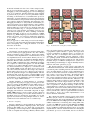
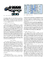
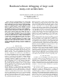
monitored information in the form of time stamped events.
The proposed monitoring system is suitable for application
debugging (1) and system debugging (2). Low level debugging
(3+4) is not addressed. Another monitoring design template
is presented in [4]. It can be used for performance analysis
and debug of the interactions of a embedded NoC processors
architecture. A generic template for bus and router monitoring
is introduced. However, the presented monitoring infrastructure
only comprises -high level debugging and monitoring (1+2).
Debugging and analysis of early software and hardware prototypes necessitates a more detailed analysis of the communication. Deadlock situations might occur and need then to be
analyzed. There are several reasons for deadlocks, ether they
result from hardware bugs or conceptual weaknesses in the
software layers. Such detailed observability (3+4) have not
been addressed explicitly yet. Time consuming conventional
hardware debugging by the use of logic analyzers or FPGA
analyzers (e.g. Xilinx ChipScope) were often used for detailed
analysis. In contrast, our concept for detailed NoC debugging
is very simple to use. It is detailed in Section III-E1 and
Section III-D.
In [5] an approach to online debug for NoC-based multiprocessor SoCs is introduced. The described debug infrastructure
allows investigating and to debug the behavior of an NoCbased SoC at run-time.
B. Virtual interfaces for debugging
Growing NoC systems require more and more debug interfaces but common prototyping platforms only offer a limited
amount of interfaces. One possibility to increase the number
of interfaces is the implementation of virtual interfaces, in [6]
one implementation has been described. Thereby all cores of
the system are connected to an Advanced eXtensible Interface
(AXI) bus. The bus is then connected to one core that is responsible for UART communication. All communication with the
host computer is redirected through the core with the UART
connection (it is named embedded virtual server). This core
is connected with the host computer by a conventional serial
line. Virtual UARTs provide each single process access to its
own serial connection. However, this concept only addresses
designs where all processors are connected to the same bus.
Due to the partitioned design over multiple FPGAs, which is
described in this work, the concept of virtual UARTs would
not be feasible. Another drawback of the virtual UART concept
is the limitation of the bandwidth to the host computer due to
the use of a single UART connection.
Another alternative of virtual interfaces is a transactor
based approach. In [7] the prototyping of a heterogeneous multiprocessor system-on-chip (MPSoC) design, which consists of
general purpose RISC processors as well as novel accelerators in form of tightly-coupled processor arrays (TCPA), is
described. The focus of this work was the transactor based
debugging and verification of the TCPA component. A single
AMBA AHB transactor is used to realize one data connection
between software running on a host PC and the hardware on
the FPGA board. As described in section III-C we use this
approach and extend it by using multiple transactors, since a
scalable NoC based architecture was not considered yet.
C. Invasive computing
Invasive computing is a novel paradigm for designing and
programming future parallel computing systems. For systems
with more than 1000 cores on a single chip, resource-aware
programming is of utmost importance to obtain high utilization
as well as computational and energy efficiency numbers. With
CPU
CPU
CPU
CPU
CPU
CPU
CPU
CPU
CPU
CPU
CPU
CPU
Memory
i-NoC
Router
Memory
i-NoC
Router
CPU
Memory
i-NoC
Router
CPU
Memory
CPU
CPU
and
CPU
CPU
CPU
CPU
I/O
Memory
i-NoC
Router
Memory
i-NoC
Router
CPU
CPU
CPU
CPU
CPU
CPU
CPU
CPU
CPU
CPU
CPU
CPU
Memory
i-NoC
Router
Fig. 1.
i-NoC
Router
Memory
Memory
i-NoC
Router
i-NoC
Router
InvasIC Network on Chip (NoC) hardware architecture
this goal in mind, invasive computing was introduced to give
a programmer explicit handles to specify and argue about
resource requirements in different phases of execution. To
support this idea of self-adaptive and resource-aware programming, new programming concepts, languages, compilers, operating systems, and hardware architectures have been
developed within the invasive research project. The invasive
hardware design of a MPSoC (multiprocessor systems-on-achip) includes profound changes to support efficiently invasion,
infection, and retreat operations. [8], [9]
The invasive Network on Chip (i-NoC) [10] builds the
communication infrastructure of the InvasIC architecture. It is
a wormhole packet switching network with Virtual Channels
(VCs) providing Quality of Service (QoS) communication by
the use of end-to-end connections as detailed in [11]. The iNoC consists of two basic components - the network adapter
(NA) and the routers which are connected via links. The iNoC routers [12] build a meshed topology and are responsible
for the data transmission between the tiles. Therefore a distributed routing scheme is realized to ensure scalability of the
architecture. The network adapter attaches the i-NoC to the
tile internal bus system. It has a memory mapped interface
and is responsible for transparent fetching of data from tile
external memories, generation of special system messages and
management of the i-NoC features. The tiles itself could be of
various types. Simple compute tiles with multiple processors,
memory and IO tiles, and also special hardware accelerator
tiles. Figure 1 shows one possible implementation of an
invasive hardware architecture.
The compute tile internal concept is based on the Gaisler
IP library [13]. It consists of several LEON3 processor cores,
different memories and several peripherals all connected to a
tile local AMBA Advanced High-performance Bus (AHB). In
addition each tile has a monitoring and a debug (DSU) unit,
as well as an AHB master transactor. The Ethernet and DDR2
memory controller are optional components, which are added
in case of a Memory and I/O tiles. Figure 2 shows one possible
implementation of the tile architecture. There are many higher
performance, processors on the market, but most of them are