1
The external bus will behave as an ADSP-2181 system
where address bits A[13:1] and data bits D[7:0] are
ignored. The upper 16 bits of the data bus can still be
used for external data transfers, but only one address bit is
available, A0. Writes to Data Memory or I/O Space will
activate the appropriate memory select(s), /RD or /WR,
place data on D[23:8], and drive a single address bit on
A0.
Program memory reads and writes behave similarly but
have the added consideration of the PX register. For
program memory reads and writes only the upper 16 bits
will be available externally. When 24 bit data is written
to external program memory the upper 16 bits will be
driven out on data bus pins [23:16]. The PX register will
still latch the lower eight bits of the program memory
word, but they will not be driven externally. If a 24 bit
read of external memory occurs, no external pins will
control the value of the PX register, and the PX register
will be written with all ones. The missing address bits
restrict using the external bus with a conventional
memory device which has separated address and data
buses. These external transfers might be usable with
shared address/data memory chips or can be used for
communication with an ASIC. The memory selects will
still be active, so each memory space is effectively
collapsed into two external addresses, address 0 and 1.
Byte Memory Accesses
BDMA accesses are still allowed in Host Mode.
However, because address pins A[13:1], now operate as
the IAD bus, construction of a complete byte address is
impossible, without external circuitry.
Byte memory addresses on the ADSP-2181 were 22-bit
addresses formed from external data pins D[23:16] and
address pins A[13:0]. In Host Mode D[23:16] and A0 are
the only address bits available externally. The values of
the external data pins D[23:16], will be the values
contained in the BMPAGE field of the BDMA Control
Register, located at internal DM address 0x3fe3 of the
processor. A0 will be 1 for odd byte addresses and 0 for
even byte addresses.
So What Does This All Mean?
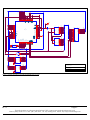
Since the DSP is configured in host mode, the external
address bus is limited to one pin, A0. What this means to
us is that we now need to use address generators to drive
the external address pins of the EPROM to facilitate
booting of the DSP. (Please refer to the included data
sheet for more information on the operation of the address
generators, Philips part number 74HC4040.)
The one caveat of building this hardware configuration is
that the address generators output sequential address
values, while the prom splitter for the 218x family does
not. So the executable file must be massaged to allow the
prom splitter to output sequential data for the eprom.
Normally, the prom splitter (when used in conjunction
with the -2181 and -loader switches), prepends a boot
loader kernel to the beginning of the eprom file. This is
done because the development tools for the 218x family
use a different boot paging scheme than the rest of the
21xx family DSP processors to initialize program
memory segments, program data segments, and data
memory segments.
The Real Solution
Here are the following steps that are needed to complete
our design:
1.
Create a system file (*.sys) for a 2101 processor that
declares on chip memory space for a 218x system,
but also includes boot page segments.
2.
Declare a boot page segment in your source code’s
.module directive.
3.
Replace the @BO symbol in your *.exe file with an
@PA symbol. (The @BO symbol is located on the
second line of the *.exe file; you can edit this file
with any text editor, since the file is written in an
ASCII file format.)
BDMA and IDMA timing and cycle stealing are the same
as on the ADSP-2181. BDMA with limited address bits
available still provides a flexible interface to the DSP.
Without full address bits addressing memory will be more
difficult but host or microcontroller communication is
possible because the order of the byte sequence is known.
For information on byte sequencing, refer to Byte Memory
Word Formats in Ch. 11 of the ADSP-2100 Family
User’s Manual.
EN-79
Page 2
Technical Notes on using Analog Devices’ DSP components and development tools
Phone: (800) ANALOG-D, FAX: (781) 461-3010, FTP: ftp.analog.com, EMAIL: [email protected]